JP6251414B2 - 調整可能なインピーダンスを提供するための回路及び方法 - Google Patents
調整可能なインピーダンスを提供するための回路及び方法 Download PDFInfo
- Publication number
- JP6251414B2 JP6251414B2 JP2016553469A JP2016553469A JP6251414B2 JP 6251414 B2 JP6251414 B2 JP 6251414B2 JP 2016553469 A JP2016553469 A JP 2016553469A JP 2016553469 A JP2016553469 A JP 2016553469A JP 6251414 B2 JP6251414 B2 JP 6251414B2
- Authority
- JP
- Japan
- Prior art keywords
- signal
- impedance
- frequency
- configuration
- electronic circuit
- Prior art date
- Legal status (The legal status is an assumption and is not a legal conclusion. Google has not performed a legal analysis and makes no representation as to the accuracy of the status listed.)
- Active
Links
- 238000000034 method Methods 0.000 title claims description 30
- 238000006243 chemical reaction Methods 0.000 claims description 56
- 230000005540 biological transmission Effects 0.000 claims description 40
- 238000004891 communication Methods 0.000 claims description 39
- 239000003990 capacitor Substances 0.000 claims description 31
- 230000003278 mimic effect Effects 0.000 claims description 10
- 238000001914 filtration Methods 0.000 claims description 3
- 230000009467 reduction Effects 0.000 description 9
- 238000010586 diagram Methods 0.000 description 8
- 230000003993 interaction Effects 0.000 description 8
- 238000013459 approach Methods 0.000 description 7
- 230000004044 response Effects 0.000 description 7
- 230000003044 adaptive effect Effects 0.000 description 5
- 238000004590 computer program Methods 0.000 description 5
- 238000005259 measurement Methods 0.000 description 5
- 238000012545 processing Methods 0.000 description 4
- 230000002238 attenuated effect Effects 0.000 description 3
- 230000001413 cellular effect Effects 0.000 description 3
- 239000004020 conductor Substances 0.000 description 3
- 238000002955 isolation Methods 0.000 description 3
- 230000010363 phase shift Effects 0.000 description 3
- 238000013461 design Methods 0.000 description 2
- 230000006870 function Effects 0.000 description 2
- 230000001939 inductive effect Effects 0.000 description 2
- 230000009471 action Effects 0.000 description 1
- 230000009286 beneficial effect Effects 0.000 description 1
- 230000010267 cellular communication Effects 0.000 description 1
- 230000008859 change Effects 0.000 description 1
- 230000008878 coupling Effects 0.000 description 1
- 238000010168 coupling process Methods 0.000 description 1
- 238000005859 coupling reaction Methods 0.000 description 1
- 230000000694 effects Effects 0.000 description 1
- 238000005516 engineering process Methods 0.000 description 1
- 230000015654 memory Effects 0.000 description 1
- 230000000630 rising effect Effects 0.000 description 1
- 230000035945 sensitivity Effects 0.000 description 1
- 230000008054 signal transmission Effects 0.000 description 1
- 238000004088 simulation Methods 0.000 description 1
Images


Classifications
-
- H—ELECTRICITY
- H04—ELECTRIC COMMUNICATION TECHNIQUE
- H04L—TRANSMISSION OF DIGITAL INFORMATION, e.g. TELEGRAPHIC COMMUNICATION
- H04L5/00—Arrangements affording multiple use of the transmission path
- H04L5/14—Two-way operation using the same type of signal, i.e. duplex
- H04L5/1461—Suppression of signals in the return path, i.e. bidirectional control circuits
-
- H—ELECTRICITY
- H04—ELECTRIC COMMUNICATION TECHNIQUE
- H04B—TRANSMISSION
- H04B1/00—Details of transmission systems, not covered by a single one of groups H04B3/00 - H04B13/00; Details of transmission systems not characterised by the medium used for transmission
- H04B1/06—Receivers
- H04B1/16—Circuits
- H04B1/18—Input circuits, e.g. for coupling to an antenna or a transmission line
-
- H—ELECTRICITY
- H04—ELECTRIC COMMUNICATION TECHNIQUE
- H04B—TRANSMISSION
- H04B1/00—Details of transmission systems, not covered by a single one of groups H04B3/00 - H04B13/00; Details of transmission systems not characterised by the medium used for transmission
- H04B1/38—Transceivers, i.e. devices in which transmitter and receiver form a structural unit and in which at least one part is used for functions of transmitting and receiving
- H04B1/40—Circuits
- H04B1/50—Circuits using different frequencies for the two directions of communication
- H04B1/52—Hybrid arrangements, i.e. arrangements for transition from single-path two-direction transmission to single-direction transmission on each of two paths or vice versa
- H04B1/525—Hybrid arrangements, i.e. arrangements for transition from single-path two-direction transmission to single-direction transmission on each of two paths or vice versa with means for reducing leakage of transmitter signal into the receiver
Landscapes
- Engineering & Computer Science (AREA)
- Signal Processing (AREA)
- Computer Networks & Wireless Communication (AREA)
- Transceivers (AREA)
- Noise Elimination (AREA)
Description
Claims (15)
- 第1周波数において調整可能なインピーダンスを提供するように構成される電子回路(51;61;71;81)であって、
前記電子回路の入力端子において入力信号を受け付け、前記入力信号に比例する第1電流信号を提供するように構成される第1相互コンダクタンス増幅器(52)と、
第1ミキサ構成(53;63;73;83)、フィルタ構成(54,55;64,65;74,75;84,85)及び第2ミキサ構成(56;66;76;86)を各々含む少なくとも1つの変換構成であって、
前記第1ミキサ構成は、前記第1周波数にあたる第1局部発振器信号を利用して、前記第1電流信号を当該ミキサ構成の出力におけるベースバンド電圧信号へとダウンコンバートするように構成され、
前記フィルタ構成は、前記第1ミキサ構成(53;63;73;83)の前記出力に接続され、少なくとも抵抗及びキャパシタを並列に含み、
前記第2ミキサ構成は、前記第1周波数にあたる第2局部発振器信号を利用して、前記フィルタ構成に現れる電圧信号を自身の出力におけるアップコンバート済み電圧信号へとアップコンバートするように構成される、
前記少なくとも1つの変換構成と、
前記アップコンバート済み電圧信号を受け付け、それに比例する第2電流信号を提供し、及び前記第2電流信号を前記電子回路の前記入力端子へとフィードバックする、ように構成される第2相互コンダクタンス増幅器(57)と、
を含む電子回路。 - 前記第1相互コンダクタンス増幅器(52)及び前記第2相互コンダクタンス増幅器(57)のうちの一方は反転相互コンダクタンス増幅器であり、他方は非反転相互コンダクタンス増幅器である、請求項1に記載の電子回路。
- 前記第1相互コンダクタンス増幅器(52)及び前記第2相互コンダクタンス増幅器(57)のうちの少なくとも一方は、制御可能な利得を有する、請求項1又は請求項2に記載の電子回路。
- 前記フィルタ構成の前記抵抗(54;64;74;84)及び前記キャパシタのうちの少なくとも一方は、制御可能である、請求項1〜3のいずれか1項に記載の電子回路。
- 前記第2局部発振器信号は、前記第1局部発振器信号を基準として位相オフセットを有する、請求項1〜4のいずれか1項に記載の電子回路。
- 前記位相オフセットは、制御可能である、請求項5に記載の電子回路。
- 前記電子回路は、2つの変換構成を含み、当該2つの変換構成の前記第1局部発振器信号は、0度とも180度とも異なる位相差を有する、請求項1〜6のいずれか1項に記載の電子回路。
- 前記2つの変換構成の前記第1局部発振器信号は、90度に等しい位相差を有する、請求項7に記載の電子回路。
- 前記電子回路は、少なくとも3つの変換構成を含み、当該変換構成の前記第1局部発振器信号は、360度にわたる対称的な位相分配を有する、請求項1〜6のいずれか1項に記載の電子回路。
- 前記電子回路は、4つの変換構成を含み、当該4つの変換構成の前記第1局部発振器信号は、直角位相群を有する、請求項9に記載の電子回路。
- 前記電子回路の前記入力端子に並列に名目インピーダンス(88)が配置される、請求項1〜10のいずれか1項に記載の電子回路。
- 共通的な入力端子へ接続される請求項1〜11のいずれか1項に記載の少なくとも2つの電子回路(92,93)を含む回路構成(91)であって、
前記少なくとも2つの電子回路(92,93)は、異なる周波数にあたる局部発振器信号を利用して、当該異なる周波数の各々において調整可能なインピーダンスを提供する、
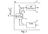
回路構成。 - 通信ネットワークとの周波数分割複信での通信のために構成される受信機(33)と、
前記通信ネットワークとの周波数分割複信での通信のために構成される送信機(32)と、
アンテナへの接続用の送信ポート(34)と、
請求項12に記載の回路構成を含み、前記送信ポートにおけるインピーダンスを模倣するように構成されるインピーダンス均衡回路(35)と、
第1タイプのフィルタ(36,37)及び第2タイプのフィルタ(38,39)を含み、前記受信機(33)、送信機(32)、送信ポート(34)及びインピーダンス均衡回路(35)を接続するフィルタ構成と、
を含み、
前記第1タイプのフィルタ(36,37)は、送信機周波数の信号を通過させ及び受信機周波数の信号を減衰させるように構成され、前記送信機(32)と前記送信ポート(34)との間、及び前記受信機(33)と前記インピーダンス均衡回路(35)との間に接続され、
前記第2タイプのフィルタ(38,39)は、送信機周波数の信号を減衰させ及び受信機周波数の信号を通過させるように構成され、前記送信機(32)と前記インピーダンス均衡回路(35)との間、及び前記受信機(33)と前記送信ポート(34)との間に接続される、
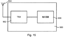
送受信機構成(95,902)。 - 請求項13に記載の送受信機構成(902)を含む、通信ネットワークを介して周波数分割複信での通信の可能な通信デバイス(900)。
- 第1周波数において調整可能なインピーダンスを提供する方法であって、
第1相互コンダクタンス増幅器により、電子回路の入力端子において受け付けた入力信号に比例する第1電流信号を提供するステップ(101)と、
少なくとも1つの変換構成の第1ミキサ構成において、前記第1周波数にあたる第1局部発振器信号を利用することにより、前記第1電流信号をベースバンド電圧信号へとダウンコンバートするステップ(102)と、
前記少なくとも1つの変換構成の少なくとも抵抗及びキャパシタを並列に含むフィルタ構成において、前記ベースバンド電圧信号をフィルタリングして、前記フィルタ構成における電圧信号を提供するステップ(103)と、
前記少なくとも1つの変換構成の第2ミキサ構成において、前記第1周波数にあたる第2局部発振器信号を利用することにより、前記フィルタ構成に現れる前記電圧信号をアップコンバート済み電圧信号へとアップコンバートするステップ(104)と、
第2相互コンダクタンス増幅器により、前記アップコンバート済み電圧信号に比例する第2電流信号を提供するステップ(105)と、
前記第2電流信号を前記電子回路の前記入力端子へとフィードバックするステップ(106)と、
を含む方法。
Applications Claiming Priority (1)
| Application Number | Priority Date | Filing Date | Title |
|---|---|---|---|
| PCT/EP2014/053371 WO2015124195A1 (en) | 2014-02-20 | 2014-02-20 | Circuit and method for providing an adjustable impedance |
Publications (2)
| Publication Number | Publication Date |
|---|---|
| JP2017511042A JP2017511042A (ja) | 2017-04-13 |
| JP6251414B2 true JP6251414B2 (ja) | 2017-12-20 |
Family
ID=50239588
Family Applications (1)
| Application Number | Title | Priority Date | Filing Date |
|---|---|---|---|
| JP2016553469A Active JP6251414B2 (ja) | 2014-02-20 | 2014-02-20 | 調整可能なインピーダンスを提供するための回路及び方法 |
Country Status (5)
| Country | Link |
|---|---|
| US (1) | US10079671B2 (ja) |
| EP (1) | EP3108587B1 (ja) |
| JP (1) | JP6251414B2 (ja) |
| IL (1) | IL247059B (ja) |
| WO (1) | WO2015124195A1 (ja) |
Families Citing this family (9)
| Publication number | Priority date | Publication date | Assignee | Title |
|---|---|---|---|---|
| US9853801B2 (en) * | 2013-10-04 | 2017-12-26 | Telefonaktiebolaget Lm Ericsson (Publ) | Transceiver arrangement, communication device, and method |
| WO2017077852A1 (ja) | 2015-11-04 | 2017-05-11 | 株式会社村田製作所 | 分波装置及びその設計方法 |
| EP3580853B1 (en) * | 2017-02-10 | 2023-04-05 | Telefonaktiebolaget LM Ericsson (publ) | Time division duplex transceiver with an integrated isolator circuit |
| JP2018198372A (ja) * | 2017-05-23 | 2018-12-13 | 京セラ株式会社 | 電子機器 |
| FR3084548B1 (fr) * | 2018-07-26 | 2020-10-02 | Univ Bordeaux | Chaine de reception et/ou d'emission a radiofrequence et procede associe |
| EP3716493B1 (en) * | 2019-03-29 | 2021-11-10 | Nokia Solutions and Networks Oy | Full duplex transmission arrangement |
| CN113892236B (zh) * | 2019-06-06 | 2023-05-12 | 华为技术有限公司 | 滤波器以及用于发射通道的电路 |
| CN112947182B (zh) * | 2021-02-05 | 2023-05-26 | 电子科技大学 | 一种提升负跨导振荡器共模瞬态抗干扰度的控制电路 |
| US20220376731A1 (en) * | 2021-05-19 | 2022-11-24 | Qualcomm Incorporated | System and method for sharing circuitry between transmit and receive path |
Family Cites Families (15)
| Publication number | Priority date | Publication date | Assignee | Title |
|---|---|---|---|---|
| GB9910454D0 (en) * | 1999-05-07 | 1999-07-07 | Koninkl Philips Electronics Nv | Circuit arrangement providing impedance translation filtering |
| GB2365235B (en) | 2000-07-20 | 2004-07-21 | British Broadcasting Corp | A circuit for simulating an impedance |
| US6549074B2 (en) * | 2000-12-05 | 2003-04-15 | Nippon Telegraph And Telephone Corporation | Transconductance amplifier, filter using the transconductance amplifier and tuning circuitry for transconductance amplifier in the filter |
| JP4588786B2 (ja) * | 2006-02-28 | 2010-12-01 | 富士通株式会社 | クロック分周回路 |
| US7949322B2 (en) * | 2007-03-09 | 2011-05-24 | Qualcomm, Incorporated | Frequency selective amplifier with wide-band impedance and noise matching |
| US8526903B2 (en) * | 2008-03-11 | 2013-09-03 | Qualcomm, Incorporated | High-linearity receiver with transmit leakage cancellation |
| US8208866B2 (en) * | 2008-08-05 | 2012-06-26 | Broadcom Corporation | RF transceiver front-end with RX/TX isolation |
| US8285241B2 (en) | 2009-07-30 | 2012-10-09 | Broadcom Corporation | Receiver apparatus having filters implemented using frequency translation techniques |
| US8208865B2 (en) * | 2009-09-11 | 2012-06-26 | Broadcom Corporation | RF front-end with on-chip transmitter/receiver isolation and noise-matched LNA |
| EP2481150A4 (en) | 2009-09-22 | 2013-11-20 | Nokia Corp | ADJUSTABLE CIRCUIT ARCHITECTURE |
| US8725085B2 (en) | 2010-06-03 | 2014-05-13 | Broadcom Corporation | RF front-end module |
| US9083441B2 (en) * | 2011-10-26 | 2015-07-14 | Qualcomm Incorporated | Impedance balancing for transmitter to receiver rejection |
| EP2587679B1 (en) | 2011-10-27 | 2015-01-07 | Nxp B.V. | Rf receiver with voltage sampling |
| US9214918B2 (en) * | 2012-03-14 | 2015-12-15 | Broadcom Corporation | Power distributing duplexer system |
| ES2533314T3 (es) * | 2012-06-07 | 2015-04-09 | Telefonaktiebolaget L M Ericsson (Publ) | Transceptor sin duplexor y aparato de comunicación |
-
2014
- 2014-02-20 JP JP2016553469A patent/JP6251414B2/ja active Active
- 2014-02-20 EP EP14708816.5A patent/EP3108587B1/en active Active
- 2014-02-20 US US15/117,219 patent/US10079671B2/en active Active
- 2014-02-20 WO PCT/EP2014/053371 patent/WO2015124195A1/en active Application Filing
-
2016
- 2016-08-02 IL IL247059A patent/IL247059B/en active IP Right Grant
Also Published As
| Publication number | Publication date |
|---|---|
| US20160352496A1 (en) | 2016-12-01 |
| EP3108587B1 (en) | 2017-07-26 |
| JP2017511042A (ja) | 2017-04-13 |
| WO2015124195A1 (en) | 2015-08-27 |
| EP3108587A1 (en) | 2016-12-28 |
| IL247059B (en) | 2018-12-31 |
| US10079671B2 (en) | 2018-09-18 |
Similar Documents
| Publication | Publication Date | Title |
|---|---|---|
| JP6251414B2 (ja) | 調整可能なインピーダンスを提供するための回路及び方法 | |
| US9793943B2 (en) | Duplexer-less transceiver and communication apparatus | |
| US10348356B2 (en) | Transmitter receiver leakage reduction in a full duplex system without the use of a duplexer | |
| US9871552B2 (en) | Transceiver arrangement, communication device, method and computer program | |
| US9900044B2 (en) | Transceiver arrangement and communication device | |
| JP6552832B2 (ja) | 二重化装置、無線デバイス、及び関連する方法 | |
| EP2989724A1 (en) | Transceiver arrangement, communication device, method and computer program | |
| US9853801B2 (en) | Transceiver arrangement, communication device, and method | |
| TW201445898A (zh) | 用於分析放大傳輸信號的傳輸佈置及方法 | |
| JP6728193B2 (ja) | トランシーバ自己干渉キャンセラのための回路及び方法 | |
| Agrawal et al. | Multi-band RF time delay element based on frequency translation |
Legal Events
| Date | Code | Title | Description |
|---|---|---|---|
| A977 | Report on retrieval |
Free format text: JAPANESE INTERMEDIATE CODE: A971007 Effective date: 20171018 |
|
| TRDD | Decision of grant or rejection written | ||
| A01 | Written decision to grant a patent or to grant a registration (utility model) |
Free format text: JAPANESE INTERMEDIATE CODE: A01 Effective date: 20171024 |
|
| A61 | First payment of annual fees (during grant procedure) |
Free format text: JAPANESE INTERMEDIATE CODE: A61 Effective date: 20171124 |
|
| R150 | Certificate of patent or registration of utility model |
Ref document number: 6251414 Country of ref document: JP Free format text: JAPANESE INTERMEDIATE CODE: R150 |
|
| R250 | Receipt of annual fees |
Free format text: JAPANESE INTERMEDIATE CODE: R250 |
|
| R250 | Receipt of annual fees |
Free format text: JAPANESE INTERMEDIATE CODE: R250 |
|
| R250 | Receipt of annual fees |
Free format text: JAPANESE INTERMEDIATE CODE: R250 |
|
| R250 | Receipt of annual fees |
Free format text: JAPANESE INTERMEDIATE CODE: R250 |