JP6251414B2 - Circuit and method for providing adjustable impedance - Google Patents
Circuit and method for providing adjustable impedance Download PDFInfo
- Publication number
- JP6251414B2 JP6251414B2 JP2016553469A JP2016553469A JP6251414B2 JP 6251414 B2 JP6251414 B2 JP 6251414B2 JP 2016553469 A JP2016553469 A JP 2016553469A JP 2016553469 A JP2016553469 A JP 2016553469A JP 6251414 B2 JP6251414 B2 JP 6251414B2
- Authority
- JP
- Japan
- Prior art keywords
- signal
- impedance
- frequency
- configuration
- electronic circuit
- Prior art date
- Legal status (The legal status is an assumption and is not a legal conclusion. Google has not performed a legal analysis and makes no representation as to the accuracy of the status listed.)
- Active
Links
- 238000000034 method Methods 0.000 title claims description 30
- 238000006243 chemical reaction Methods 0.000 claims description 56
- 230000005540 biological transmission Effects 0.000 claims description 40
- 238000004891 communication Methods 0.000 claims description 39
- 239000003990 capacitor Substances 0.000 claims description 31
- 230000003278 mimic effect Effects 0.000 claims description 10
- 238000001914 filtration Methods 0.000 claims description 3
- 230000009467 reduction Effects 0.000 description 9
- 238000010586 diagram Methods 0.000 description 8
- 230000003993 interaction Effects 0.000 description 8
- 238000013459 approach Methods 0.000 description 7
- 230000004044 response Effects 0.000 description 7
- 230000003044 adaptive effect Effects 0.000 description 5
- 238000004590 computer program Methods 0.000 description 5
- 238000005259 measurement Methods 0.000 description 5
- 238000012545 processing Methods 0.000 description 4
- 230000002238 attenuated effect Effects 0.000 description 3
- 230000001413 cellular effect Effects 0.000 description 3
- 239000004020 conductor Substances 0.000 description 3
- 238000002955 isolation Methods 0.000 description 3
- 230000010363 phase shift Effects 0.000 description 3
- 238000013461 design Methods 0.000 description 2
- 230000006870 function Effects 0.000 description 2
- 230000001939 inductive effect Effects 0.000 description 2
- 230000009471 action Effects 0.000 description 1
- 230000009286 beneficial effect Effects 0.000 description 1
- 230000010267 cellular communication Effects 0.000 description 1
- 230000008859 change Effects 0.000 description 1
- 230000008878 coupling Effects 0.000 description 1
- 238000010168 coupling process Methods 0.000 description 1
- 238000005859 coupling reaction Methods 0.000 description 1
- 230000000694 effects Effects 0.000 description 1
- 238000005516 engineering process Methods 0.000 description 1
- 230000015654 memory Effects 0.000 description 1
- 230000000630 rising effect Effects 0.000 description 1
- 230000035945 sensitivity Effects 0.000 description 1
- 230000008054 signal transmission Effects 0.000 description 1
- 238000004088 simulation Methods 0.000 description 1
Images


Classifications
-
- H—ELECTRICITY
- H04—ELECTRIC COMMUNICATION TECHNIQUE
- H04L—TRANSMISSION OF DIGITAL INFORMATION, e.g. TELEGRAPHIC COMMUNICATION
- H04L5/00—Arrangements affording multiple use of the transmission path
- H04L5/14—Two-way operation using the same type of signal, i.e. duplex
- H04L5/1461—Suppression of signals in the return path, i.e. bidirectional control circuits
-
- H—ELECTRICITY
- H04—ELECTRIC COMMUNICATION TECHNIQUE
- H04B—TRANSMISSION
- H04B1/00—Details of transmission systems, not covered by a single one of groups H04B3/00 - H04B13/00; Details of transmission systems not characterised by the medium used for transmission
- H04B1/06—Receivers
- H04B1/16—Circuits
- H04B1/18—Input circuits, e.g. for coupling to an antenna or a transmission line
-
- H—ELECTRICITY
- H04—ELECTRIC COMMUNICATION TECHNIQUE
- H04B—TRANSMISSION
- H04B1/00—Details of transmission systems, not covered by a single one of groups H04B3/00 - H04B13/00; Details of transmission systems not characterised by the medium used for transmission
- H04B1/38—Transceivers, i.e. devices in which transmitter and receiver form a structural unit and in which at least one part is used for functions of transmitting and receiving
- H04B1/40—Circuits
- H04B1/50—Circuits using different frequencies for the two directions of communication
- H04B1/52—Hybrid arrangements, i.e. arrangements for transition from single-path two-direction transmission to single-direction transmission on each of two paths or vice versa
- H04B1/525—Hybrid arrangements, i.e. arrangements for transition from single-path two-direction transmission to single-direction transmission on each of two paths or vice versa with means for reducing leakage of transmitter signal into the receiver
Landscapes
- Engineering & Computer Science (AREA)
- Signal Processing (AREA)
- Computer Networks & Wireless Communication (AREA)
- Transceivers (AREA)
- Noise Elimination (AREA)
Description
本発明は、所与の1つ又は複数の周波数で調整可能なインピーダンスを提供するように構成される電子回路、回路構成、送受信機構成、及び調整可能なインピーダンスを提供する方法に関する。 The present invention relates to electronic circuits, circuit configurations, transceiver configurations, and methods for providing adjustable impedance that are configured to provide adjustable impedance at a given frequency or frequencies.
所与の周波数(若しくは複数の周波数)又は周波数レンジ(若しくは複数のレンジ)で調整可能なインピーダンスを提供できる回路が望ましく又は有利となるような、いくつかのアプリケーションが存在する。 There are a number of applications where a circuit capable of providing an adjustable impedance at a given frequency (or frequencies) or frequency range (or ranges) is desirable or advantageous.
1つの例は、多様な通信デバイス内で共通的に使用され、送信機と共に受信機を含む、送受信機である。 One example is a transceiver that is commonly used in various communication devices and includes a receiver along with a transmitter.
そうした送受信機は、半二重(semi-duplex)で動作するように構成されることができ、即ち、送信信号が受信信号を覆い隠してしまうことを防止するために受信機及び送信機は分けられた時間において動作する。従って、このアプローチを、通常、時間分割複信(TDD)という。 Such a transceiver can be configured to operate in semi-duplex, ie the receiver and transmitter are separated to prevent the transmitted signal from obscuring the received signal. Operate at a given time. Therefore, this approach is usually referred to as time division duplex (TDD).
また、送受信機を全二重(full duplex)で動作させることもでき、即ち、受信機及び送信機は同時に動作する。このケースでは、送信機が受信信号を覆い隠してしまうことを防止するための構成が提供される。これを達成する1つのアプローチは、送信及び受信に異なる周波数を割り当てることである。従って、このアプローチを、通常、周波数分割複信(FDD)という。しばしば、受信機及び送信機は、同じアンテナ又は複数のアンテナを含み得るアンテナシステムを使用し、これはある種の回路がアンテナとの適切な相互作用を可能とするように望まれ得ることを示唆する。その回路は、FDDを用いるとしても送信機が受信信号に干渉しかねず、即ち送受信機内の内部的な干渉があり得ることから、全二重で送受信機を動作させる際の何らかの手当てと共に作られるべきである。 It is also possible to operate the transceiver in full duplex, i.e. the receiver and transmitter operate simultaneously. In this case, a configuration is provided to prevent the transmitter from covering up the received signal. One approach to accomplish this is to assign different frequencies for transmission and reception. Therefore, this approach is usually referred to as frequency division duplex (FDD). Often, the receiver and transmitter use an antenna system that can include the same antenna or multiple antennas, suggesting that certain circuits may be desired to allow proper interaction with the antenna. To do. The circuit is made with some precautions when operating the transmitter in full duplex, even if FDD is used, the transmitter can interfere with the received signal, i.e. there may be internal interference in the transmitter / receiver. Should.
言い換えれば、FDDセルラー無線機器のための受信機は、それ自身の送信機からの非常に強力な信号の影響を受けることになり得る。それら強力な送信信号は、受信チャネルからの複信距離に存在する。典型的な複信距離は、キャリア周波数と比較すると小さい(典型的には、100MHzよりも少ない)。受信機は、良好な感受性を達成するために、それら電力レベルの高い信号から遮蔽され又は隔離されなければならない。現在のところ、これは、デュプレクサと呼ばれるオフチップの音波デュプレックスフィルタを用いることにより達成され得る。デュプレクサは、無線周波数(RF)信号を送信機からアンテナへと、及びアンテナから受信機へと方向付けるように構成される。それは、例えばサーキュレータを含んでもよい。残念ながら、デュプレクサは、高価かつ嵩張り、よって部品点数と所要の基盤面積とを増加させる。オンチップでデュプレクサを実装することもまた困難である。これは、サポートすべき周波数帯の数が増えることによってさらに顕著になる。従って、隔離機能をなす統合的な解決策が強く望まれている。 In other words, a receiver for an FDD cellular radio device can be affected by a very strong signal from its own transmitter. These strong transmitted signals exist at a duplex distance from the receiving channel. The typical duplex distance is small compared to the carrier frequency (typically less than 100 MHz). Receivers must be shielded or isolated from these high power level signals to achieve good sensitivity. At present, this can be accomplished by using an off-chip sonic duplex filter called a duplexer. The duplexer is configured to direct radio frequency (RF) signals from the transmitter to the antenna and from the antenna to the receiver. It may include, for example, a circulator. Unfortunately, duplexers are expensive and bulky, thus increasing the number of parts and the required base area. It is also difficult to implement a duplexer on-chip. This becomes even more pronounced as the number of frequency bands to be supported increases. Therefore, an integrated solution for the isolation function is highly desired.
オンチップの隔離デバイスを実現するためのいくつかの解決策が存在する。1つの例は、US2011/064004に開示されている。US2011/064004には、電気的均衡によって隔離を提供するRFフロントエンドが示されている。それは、キャンセレーションに基づいており、変圧器(transformer)を使用する。受信機入力にて発生する送信信号のキャンセルのために、対称性が必要であり、よって回路はダミーの負荷又は均衡用インピーダンスを要し、それは完全なキャンセレーションのためにアンテナインピーダンスに等しいものとされる。開示されている均衡ネットワークはチューニング可能ではあるものの、アンテナインピーダンスが複合的(誘導性又は容量性)であること及び周波数に加えてアンテナ環境と共に変化することを考慮していない。さらに、キャリア周波数と比較すると小さいものの受信周波数及び送信周波数がアンテナについて大きく異なるインピーダンスが現れる程度には離れていることから必要とされる、受信周波数及び送信周波数で別々にチューニング可能なインピーダンスを、開示されている均衡ネットワークは提供することができない。 There are several solutions for realizing on-chip isolation devices. One example is disclosed in US2011 / 064004. US 2011/064004 shows an RF front end that provides isolation by electrical balance. It is based on cancellation and uses a transformer. Symmetry is required for cancellation of the transmitted signal occurring at the receiver input, so the circuit requires a dummy load or balancing impedance, which is equal to the antenna impedance for complete cancellation. Is done. Although the disclosed balanced network is tunable, it does not take into account that the antenna impedance is complex (inductive or capacitive) and changes with the antenna environment in addition to frequency. Furthermore, the impedance that can be tuned separately at the reception frequency and the transmission frequency, which is required because the reception frequency and the transmission frequency are small as compared with the carrier frequency, but are separated from each other to the extent that impedances greatly differ with respect to the antenna, are disclosed. The balanced network that is being used cannot be provided.
従って、本発明の実施形態の目的は、所与の周波数又は狭い周波数レンジで調整可能なインピーダンスを提供し、同時にその周波数又は周波数レンジから離れた周波数では高いインピーダンスを提供することのできる電子回路を提供し、それにより、異なる周波数にチューニングされた2つ以上の回路を並列に連結して近傍の周波数で異なるインピーダンスを提供することを可能とすることである。 Accordingly, an object of embodiments of the present invention is to provide an electronic circuit that can provide a tunable impedance at a given frequency or narrow frequency range and at the same time provide a high impedance at frequencies away from that frequency or frequency range. Providing, thereby allowing two or more circuits tuned to different frequencies to be connected in parallel to provide different impedances at nearby frequencies.
本発明の実施形態によれば、上記目標は、第1周波数において調整可能なインピーダンスを提供するように構成される電子回路によって達成される。その回路は、上記電子回路の入力端子において入力信号を受け付け、上記入力信号に比例する第1電流信号を提供するように構成される第1相互コンダクタンス増幅器と、第1ミキサ構成、フィルタ構成及び第2ミキサ構成を各々含む少なくとも1つの変換構成であって、上記第1ミキサ構成は、上記第1周波数にあたる第1局部発振器信号を利用して、上記第1電流信号を当該ミキサ構成の出力におけるベースバンド電圧信号へとダウンコンバートするように構成され、上記フィルタ構成は、上記第1ミキサ構成の上記出力に接続され、少なくとも抵抗及びキャパシタを並列に含み、上記第2ミキサ構成は、上記第1周波数にあたる第2局部発振器信号を利用して、上記フィルタ構成に現れる電圧信号を自身の出力におけるアップコンバート済み電圧信号へとアップコンバートするように構成される、上記少なくとも1つの変換構成と、上記アップコンバート済み電圧信号を受け付け、それに比例する第2電流信号を提供し、及び上記第2電流信号を上記電子回路の上記入力端子へとフィードバックする、ように構成される第2相互コンダクタンス増幅器と、を含む。 According to an embodiment of the present invention, the above goal is achieved by an electronic circuit configured to provide an adjustable impedance at the first frequency. The circuit receives an input signal at an input terminal of the electronic circuit and provides a first transconductance amplifier configured to receive a first current signal proportional to the input signal, a first mixer configuration, a filter configuration, and a first At least one conversion configuration including each of two mixer configurations, wherein the first mixer configuration utilizes a first local oscillator signal corresponding to the first frequency to convert the first current signal to a base at the output of the mixer configuration. Configured to downconvert to a band voltage signal, wherein the filter configuration is connected to the output of the first mixer configuration, includes at least a resistor and a capacitor in parallel, and the second mixer configuration includes the first frequency Using the second local oscillator signal corresponding to the above, the voltage signal appearing in the filter configuration is converted to an up-converter at its output. The at least one conversion arrangement configured to upconvert to a finished voltage signal; accepting the upconverted voltage signal; providing a second current signal proportional thereto; and A second transconductance amplifier configured to feed back to the input terminal of the electronic circuit.
この手法で上記第1ミキサ構成及び上記第2ミキサ構成を使用することにより、(狭帯域ベースバンドインピーダンスとみなすこともできる)抵抗及びキャパシタと共に実装されるフィルタ構成を、無線周波数へとアップコンバートすることができる。この手法で、高い品質係数に対応するシャープな周波数応答を、品質係数の非常に高いインダクタを必要とすることなく、周波数変換技法を用いて達成することができる。ベースバンドインピーダンスの帯域幅を十分に狭くすることにより、2つ以上の変換後インピーダンス回路を、近傍の周波数にて限られた相互作用と共に使用することができる。 By using the first mixer configuration and the second mixer configuration in this manner, a filter configuration implemented with a resistor and a capacitor (which can be regarded as a narrowband baseband impedance) is upconverted to a radio frequency. be able to. With this approach, a sharp frequency response corresponding to a high quality factor can be achieved using frequency conversion techniques without the need for an inductor with a very high quality factor. By sufficiently narrowing the bandwidth of the baseband impedance, two or more post-conversion impedance circuits can be used with limited interaction at nearby frequencies.
いくつかの実施形態において、上記第1相互コンダクタンス増幅器及び上記第2相互コンダクタンス増幅器のうちの一方は反転相互コンダクタンス増幅器であり、他方は非反転相互コンダクタンス増幅器である。これは、回路の低周波数での安定性を確実化する。 In some embodiments, one of the first transconductance amplifier and the second transconductance amplifier is an inverting transconductance amplifier and the other is a non-inverting transconductance amplifier. This ensures the low frequency stability of the circuit.
上記第1相互コンダクタンス増幅器及び上記第2相互コンダクタンス増幅器のうちの少なくとも一方が制御可能な利得を有する場合、提供されるインピーダンスの大きさをその制御可能な相互コンダクタンス増幅器の利得を制御することにより調整することができる。上記フィルタ構成の上記抵抗及び上記キャパシタのうちの少なくとも一方が制御可能である場合、同様の結果を達成することができる。 If at least one of the first transconductance amplifier and the second transconductance amplifier has a controllable gain, the magnitude of the impedance provided is adjusted by controlling the gain of the controllable transconductance amplifier can do. Similar results can be achieved if at least one of the resistor and the capacitor of the filter configuration is controllable.
上記第2局部発振器信号が上記第1局部発振器信号を基準とする位相オフセットを有する場合、インピーダンスに異なる位相角を提供することができる。上記位相オフセットが制御可能である場合、提供されるインピーダンスの位相角もまた制御されることができる。 If the second local oscillator signal has a phase offset relative to the first local oscillator signal, a different phase angle can be provided for the impedance. If the phase offset is controllable, the phase angle of the provided impedance can also be controlled.
上記電子回路は、2つの変換構成の上記第1局部発振器信号が0度とも180度とも異なる位相差を有する当該2つの変換構成を含んでもよい。この手法で、上記回路に、当該回路への入力信号が上記第1局部発振器信号と同じ周波数及び同じ位相を有しない状況において、所望のインピーダンスを提供することもまた可能となる。1つの実施形態において、上記2つの変換構成の上記第1局部発振器信号は、90度に等しい位相差を有する。 The electronic circuit may include the two conversion configurations in which the first local oscillator signal of the two conversion configurations has a phase difference different from both 0 degrees and 180 degrees. In this manner, it is also possible to provide the circuit with a desired impedance in situations where the input signal to the circuit does not have the same frequency and phase as the first local oscillator signal. In one embodiment, the first local oscillator signal of the two conversion configurations has a phase difference equal to 90 degrees.
代替的に、上記電子回路は、変換構成の上記第1局部発振器信号が360度にわたる対称的な位相分配を有する少なくとも3つの変換構成を含んでもよい。1つの実施形態において、上記電子回路は、4つの変換構成を含み、当該4つの変換構成の上記第1局部発振器信号は、直角位相群(quadrature phases)を有する。 Alternatively, the electronic circuit may include at least three conversion configurations in which the first local oscillator signal of the conversion configuration has a symmetric phase distribution spanning 360 degrees. In one embodiment, the electronic circuit includes four conversion configurations, and the first local oscillator signal of the four conversion configurations has quadrature phases.
名目インピーダンスが上記電子回路の上記入力端子に並列に配置されてもよい。 A nominal impedance may be placed in parallel with the input terminal of the electronic circuit.
ある回路構成は、共通的な入力端子へ接続される上述したような少なくとも2つの電子回路を含んでよく、上記少なくとも2つの電子回路は、異なる周波数にあたる局部発振器信号を利用して、当該異なる周波数の各々において調整可能なインピーダンスを提供する。この手法で、上記回路構成は、送受信機の受信周波数及び送信周波数などといった異なる周波数において異なるインピーダンスを同時に提供することができる。 A circuit configuration may include at least two electronic circuits, as described above, connected to a common input terminal, the at least two electronic circuits utilizing local oscillator signals at different frequencies and using the different frequencies. Each providing an adjustable impedance. In this manner, the circuit configuration can simultaneously provide different impedances at different frequencies, such as the reception and transmission frequencies of the transceiver.
ある送受信機構成は、通信ネットワークとの周波数分割複信での通信のために構成される受信機と、上記通信ネットワークとの周波数分割複信での通信のために構成される送信機と、アンテナへの接続用の送信ポートと、上述したような回路構成を含み、上記送信ポートにおけるインピーダンスを模倣(mimic)するように構成されるインピーダンス均衡回路と、第1タイプのフィルタ及び第2タイプのフィルタを含み、上記受信機、送信機、送信ポート及びインピーダンス均衡回路を接続するフィルタ構成と、を含んでよく、上記第1タイプのフィルタは、送信機周波数の信号を通過させ及び受信機周波数の信号を減衰させるように構成され、上記送信機と上記送信ポートとの間、及び上記受信機と上記インピーダンス均衡回路との間に接続され、上記第2タイプのフィルタは、送信機周波数の信号を減衰させ及び受信機周波数の信号を通過させるように構成され、上記送信機と上記インピーダンス均衡回路との間、及び上記受信機と上記送信ポートとの間に接続される。 A transceiver configuration includes a receiver configured for communication in frequency division duplex with a communication network, a transmitter configured for communication in frequency division duplex with the communication network, and an antenna. A transmission port for connection to a network, an impedance balancing circuit including a circuit configuration as described above and configured to mimic an impedance in the transmission port, a first type filter and a second type filter A filter arrangement connecting the receiver, transmitter, transmission port and impedance balance circuit, wherein the first type of filter passes a signal at the transmitter frequency and a signal at the receiver frequency. Connected between the transmitter and the transmission port, and between the receiver and the impedance balancing circuit. The second type filter is configured to attenuate a transmitter frequency signal and pass a receiver frequency signal, between the transmitter and the impedance balancing circuit, and between the receiver and the Connected to the transmission port.
上記送受信機構成は、上記受信機の入力ポートの少なくとも1つの端子において振幅検出器構成をさらに含んでよく、上記送受信機構成は、上記受信機の入力ポートの上記少なくとも1つの端子における振幅が上記振幅検出器構成による測定結果に基づいて低減されるように、上記インピーダンス均衡回路の調整可能なインピーダンスを制御する、ように構成されるコントローラ、を含む。この手法で、上記インピーダンス均衡回路を、アンテナインピーダンスを模倣するように制御することができる。 The transceiver configuration may further include an amplitude detector configuration at at least one terminal of the input port of the receiver, wherein the transceiver configuration has an amplitude at the at least one terminal of the input port of the receiver as described above. A controller configured to control an adjustable impedance of the impedance balance circuit to be reduced based on measurement results from the amplitude detector configuration. In this way, the impedance balancing circuit can be controlled to mimic the antenna impedance.
上記コントローラは、上記第1相互コンダクタンス増幅器の制御可能な利得、上記第2相互コンダクタンス増幅器の制御可能な利得、及び上記フィルタ構成の上記抵抗、のうちの少なくとも1つを制御することにより、上記インピーダンス均衡回路の上記調整可能なインピーダンスの大きさを制御する、ように構成されてもよい。 The controller controls the impedance by controlling at least one of a controllable gain of the first transconductance amplifier, a controllable gain of the second transconductance amplifier, and the resistance of the filter configuration. It may be configured to control the adjustable impedance magnitude of the balanced circuit.
上記コントローラは、上記第1局部発振器信号を基準とする上記第2局部発振器信号の位相オフセットを制御することにより、上記インピーダンス均衡回路の上記調整可能なインピーダンスの位相を制御する、ようにさらに構成されてもよい。 The controller is further configured to control the phase of the adjustable impedance of the impedance balancing circuit by controlling a phase offset of the second local oscillator signal relative to the first local oscillator signal. May be.
通信ネットワークを介して周波数分割複信での通信の可能な通信デバイスは、上述したような送受信機構成を含んでもよい。 A communication device capable of communication by frequency division duplex via a communication network may include a transceiver configuration as described above.
言及したように、本発明は、第1周波数において調整可能なインピーダンスを提供する方法にさらに関する。当該方法は、第1相互コンダクタンス増幅器により、電子回路の入力端子において受け付けた入力信号に比例する第1電流信号を提供するステップと、少なくとも1つの変換構成の第1ミキサ構成において、上記第1周波数にあたる第1局部発振器信号を利用することにより、上記第1電流信号をベースバンド電圧信号へとダウンコンバートするステップと、上記少なくとも1つの変換構成の少なくとも抵抗及びキャパシタを並列に含むフィルタ構成において、上記ベースバンド電圧信号をフィルタリングして、上記フィルタ構成における電圧信号を提供するステップと、上記少なくとも1つの変換構成の第2ミキサ構成において、上記第1周波数にあたる第2局部発振器信号を利用することにより、上記フィルタ構成に現れる上記電圧信号をアップコンバート済み電圧信号へとアップコンバートするステップと、第2相互コンダクタンス増幅器により、上記アップコンバート済み電圧信号に比例する第2電流信号を提供するステップと、上記第2電流信号を上記電子回路の上記入力端子へとフィードバックするステップと、を含む。 As mentioned, the present invention further relates to a method for providing an adjustable impedance at a first frequency. The method includes providing, by a first transconductance amplifier, a first current signal proportional to an input signal received at an input terminal of an electronic circuit, and in a first mixer configuration of at least one conversion configuration, the first frequency A step of downconverting the first current signal to a baseband voltage signal by utilizing a corresponding first local oscillator signal, and a filter configuration including at least a resistor and a capacitor in parallel in the at least one conversion configuration, Filtering a baseband voltage signal to provide a voltage signal in the filter configuration, and utilizing a second local oscillator signal corresponding to the first frequency in the second mixer configuration of the at least one conversion configuration, The voltage signal appearing in the filter configuration Up-converting to an up-converted voltage signal, providing a second current signal proportional to the up-converted voltage signal by a second transconductance amplifier, and converting the second current signal to the electronic circuit Feeding back to the input terminal.
この手法で上記第1ミキサ構成及び上記第2ミキサ構成を使用することにより、(狭帯域ベースバンドインピーダンスとみなすこともできる)抵抗及びキャパシタと共に実装されるフィルタ構成を、無線周波数へとアップコンバートすることができる。この手法で、高い品質係数に対応するシャープな周波数応答を、品質係数の非常に高いインダクタを必要とすることなく、周波数変換技法を用いて達成することができる。ベースバンドインピーダンスの帯域幅を十分に狭くすることにより、2つ以上の変換後インピーダンス回路を、近傍の周波数にて限られた相互作用と共に使用することができる。 By using the first mixer configuration and the second mixer configuration in this manner, a filter configuration implemented with a resistor and a capacitor (which can be regarded as a narrowband baseband impedance) is upconverted to a radio frequency. be able to. With this approach, a sharp frequency response corresponding to a high quality factor can be achieved using frequency conversion techniques without the need for an inductor with a very high quality factor. By sufficiently narrowing the bandwidth of the baseband impedance, two or more post-conversion impedance circuits can be used with limited interaction at nearby frequencies.
上記方法は、上記第1相互コンダクタンス増幅器の制御可能な利得、上記第2相互コンダクタンス増幅器の制御可能な利得、及び上記フィルタ構成の上記抵抗、のうちの少なくとも1つを制御することにより、上記調整可能なインピーダンスの大きさを制御するステップ、をさらに含んでもよい。 The method includes controlling the at least one of a controllable gain of the first transconductance amplifier, a controllable gain of the second transconductance amplifier, and the resistance of the filter configuration. The method may further include the step of controlling the magnitude of possible impedance.
上記方法は、上記第1局部発振器信号を基準とする上記第2局部発振器信号の位相オフセットを制御することにより、上記調整可能なインピーダンスの位相を制御するステップ、をさらに含んでもよい。 The method may further include controlling the phase of the adjustable impedance by controlling a phase offset of the second local oscillator signal relative to the first local oscillator signal.
本発明の実施形態が、次の図面を参照しながら、より十分に以下に説明されるであろう。 Embodiments of the present invention will be described more fully hereinafter with reference to the following drawings.
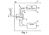
本発明の実施形態の利用の一例を示すために、図1は、周波数分割複信(FDD)セルラー無線機器の送受信機の形式の既知の通信回路を示している。送受信機1は、送信機2及び受信機3を備え、それらは共に共通アンテナ4へと接続されている。周波数分割複信送受信機において、送信機及び受信機は、同じ周波数帯域内の、いわゆる複信距離だけ離隔された異なる周波数を使用し、複信距離は通常、キャリア周波数と比較すると小さい(典型的には100MHzよりも少ない)。これは、矢印5により示したアンテナ4から受信される信号に加えて、矢印6により示したように、受信機3もまた送受信機それ自体の送信機2からの非常に強力な信号の影響を受けることを意味する。
To illustrate an example of the use of an embodiment of the present invention, FIG. 1 shows a known communication circuit in the form of a transceiver of a frequency division duplex (FDD) cellular radio device. The transceiver 1 includes a
受信機3は、電力レベルの高いそれら信号から、音波デュプレックスフィルタであり得るデュプレクサ7により遮蔽され又は隔離される。デュプレクサ7は、無線周波数(RF)信号を送信機2からアンテナ4へと、及びアンテナ4から受信機3へと方向付けるように構成される。残念ながら、デュプレクサは、高価かつ嵩張り、よって送信機の部品点数と所要の基盤面積とを増加させる。オンチップでデュプレクサを実装することもまた困難である。これは、サポートすべき周波数帯の数が増えることによってさらに顕著になる。
The receiver 3 is shielded or isolated from those signals with high power levels by a
図2は、オンチップの解決策で同様の作用を達成しようとする送受信機11の一例を示しており、完全なキャンセレーションのためにアンテナインピーダンスと等しくなる(模倣する)ように構成されるダミーの負荷又は均衡用インピーダンスを用いた電気的均衡に基づく。送受信機11は、送信機12、受信機13及びアンテナ14を備える。送信機12は、アンテナ14へ向かうキャパシタ18及びインダクタ19を含むブランチと、ダミー負荷22へ向かうキャパシタ20及びインダクタ21を含むブランチとの双方へと自身の出力信号を提供する。ダミー負荷22は、アンテナ14のインピーダンスを模倣するように構成され、達成される対称性によって、変圧器23を介する受信機13への差動入力を用いる場合に、受信機にて送信信号から入り込む寄与成分が抑圧される。この解決策の欠点は、ダミー負荷22において信号エネルギーの半分が失われることである。他の欠点は、変圧器が必要なことであり、これは例えばオンチップでの、低コスト及び/又は小さいスペース消費での実装を難しくし得る。以下では、ダミー負荷又は均衡用インピーダンス22をどのように実装することができるかが説明されるであろう。
FIG. 2 shows an example of a
送受信機自身の送信機からの強力な信号から受信機を隔離することのできる送受信機31の他の例が、図3に提案されている。送受信機31は、無線通信ネットワークとの周波数分割複信での通信のために構成される受信機33と、無線通信ネットワークとの周波数分割複信での通信のために構成される送信機32と、アンテナへの接続用のアンテナポート34と、アンテナポート34におけるインピーダンスを模倣するように構成される適応的インピーダンスを提供するように構成されるインピーダンス均衡回路35と、を備える。インピーダンス均衡回路35は、動作時にアンテナポート34へ接続されるアンテナにより現れる負荷を模倣するダミー負荷であるということもできる。
Another example of a
受信機33は、差動的に動作し、共通モード信号には応答せず、即ち、受信機33の2つの入力において同一の信号が受信される場合には理想的には出力信号は何も生じない。インピーダンス均衡回路35がアンテナポート34におけるインピーダンスを完全に模倣する場合に、これによって受信機の入力において送信機信号の寄与成分のキャンセルがなされる。なぜなら、その場合に送信機信号は受信機において共通モードとなるからである。
The receiver 33 operates differentially and does not respond to the common mode signal, i.e., ideally no output signal is received when the same signal is received at the two inputs of the receiver 33. Does not occur. If the
受信機入力における送信機信号の寄与成分は、対称的に配置され且つ送信機32から受信機33への2つのパスを基準に対称的な値を与えられたフィルタ36、37、38、39によってさらに低減される。しかしながら、以下に解明されるように、それらは、送信機32からアンテナポート34及びインピーダンス均衡回路35へ向かう通過信号、並びにアンテナポート34及びインピーダンス均衡回路35から受信機33へ向かう通過信号の観点では対称的ではない。
The contributing component of the transmitter signal at the receiver input is provided by
フィルタ36、37は、送信周波数の信号を通過させ及び受信周波数の信号を減衰させるように構成される第1タイプである。送信周波数及び受信周波数は、上述したように複信距離だけ相違する。フィルタ38、39は、受信周波数の信号を通過させ及び送信周波数の信号を減衰させるように構成される第2タイプである。
The
よって、送信機32からの送信周波数の信号は、アンテナポート34へ接続されるアンテナを通じて効率的に送信されることが可能となるように、フィルタ36を介してアンテナポート34へ向けて通過する。また、フィルタ36は、受信周波数の送信機ノイズを抑圧し、よってフィルタ39により受信機入力へ渡される干渉が低減される。送信機信号は、フィルタ39によって減衰されて、受信機33の入力における干渉が低減される。送信機信号は、インピーダンス均衡回路35において非常に少ない送信エネルギーしか無駄とならないようにフィルタ38によって減衰させられ、よってフィルタ38は、フィルタ37上の経路を介して受信機33へ到達可能な送信エネルギーを低減し、フィルタ37は干渉を低減する。
Therefore, a signal having a transmission frequency from the
アンテナポート34へ接続されたアンテナからの受信信号は、フィルタ39を介して受信機33へ到達し、フィルタ39は、受信信号を通過させるが、アンテナポートにやはり現れる送信信号を減衰させる。受信機33の入力は、フィルタ37を介してインピーダンス均衡回路35にも接続され、フィルタ37は、インピーダンス均衡回路35により生成されるノイズがほんの少ししか受信機33に到達せず且つほんの少しの受信信号の信号エネルギーしかインピーダンス均衡回路35において無駄とならないように、受信信号をやはり減衰させる。受信信号は、共通モード信号低減回路40に起因して受信機の双方の入力ノードに現れる。共通モード信号低減回路40は、以下に説明されるであろう。
The received signal from the antenna connected to the
このように、送受信機31は、送信機からアンテナポート信号を効率的に提供し、アンテナポートから受信機へ信号を効率的に提供し、同時に送信機から受信機へ到達する干渉信号を低減する構造を提供する。
In this way, the
受信機入力における送信機信号による総寄与成分をゼロの近くに維持するためには対称性が望ましく、即ち、受信機33の差動入力端子の一方へのフィルタ36、アンテナポート34及びフィルタ39の経路、並びに受信機33の差動入力端子の他方へのフィルタ38、インピーダンス均衡回路35及びフィルタ37の経路、という対称的な経路を通じてキャンセレーションが生じることになる。これは、複数の経路において同じタイプのフィルタを使用すること、及びインピーダンス均衡回路35のインピーダンスをアンテナポート34におけるインピーダンスを模倣するように適応させることにより達成される。
Symmetry is desirable to keep the total contribution due to the transmitter signal at the receiver input close to zero, ie, the
差動受信機入力ポートにおける送信機信号のキャンセレーションを達成するために、信号の伝達は、送信機32から受信機33への2つの経路において好適には等しい。すると、送信機からの信号は、受信機入力ポートにおいて完全に共通モードであるように見えるであろう。このようにするためには、フィルタは、2つの経路において互いに反対の順序であるにも関わらず、同じインピーダンスによって終端される。回路の動作は、次のようにして良好に説明され得る。まず、増幅器48が理想的であって、インピーダンス45、46がゼロであるものと仮定する。そして、送信機は、2つのフィルタ36及び38を、それらの間がゼロインピーダンスであることに対応する、同じ電圧で駆動する。受信機入力ノードにおけるゼロの共通モードインピーダンスによってフィルタ37及び39を終端することにより、受信機33への送信機漏洩が共通モードに見えるように、対称性が確実化される。ゼロの共通モードインピーダンス、即ち短絡は、送信機の干渉に起因する電圧が受信機入力において高まることを妨げ、受信機の設計を簡略化し、強力な共通モード信号を扱って多大な共通モードの除去を提供する必要を無くすであろう。
In order to achieve the cancellation of the transmitter signal at the differential receiver input port, the signal transmission is preferably equal in the two paths from the
共通モードの除去は、アンテナポート34から受信機33へ信号が通過することを依然として許容するであろう。なぜなら、それらは非対称的に、即ち受信機入力への上側のブランチにだけ入ってくるからである。但し、共通モード信号低減回路40は、アンテナ信号が受信機入力端子の双方に現れることになるように差動入力信号を保証することに留意されたい。共通モード信号低減回路40は、共通モード信号について低インピーダンスを提供する。
The removal of the common mode will still allow the signal to pass from the
共通モード信号低減回路40は、反転増幅器48、第1インピーダンス41、第2インピーダンス42、第3インピーダンス43、及び第4インピーダンス44を含む。反転増幅器48の入力は、等しいインピーダンスを有する第1インピーダンス41及び第2インピーダンス42の間の電圧の分割によって提供され、即ち、当該電圧は均等に分けられる。電圧分割後の信号は、よって、それら経路を通じて提供される共通モード信号に対応するであろう。増幅器48の出力は、等しいインピーダンスを有する第3インピーダンス43及び第4インピーダンス44の接点へと提供され、それにより対称性が提供される。第1インピーダンス41及び第2インピーダンス42、並びに第3インピーダンス43及び第4インピーダンス44は、第1タイプのフィルタ37及び第2タイプのフィルタ39の間でそれぞれ直列に接続され、それらもまた受信機33の入力端子である。よって、反転増幅器48は、インピーダンス41及び42により検出される共通モードの電圧に応じた出力を提供することになり、それは第3インピーダンス43及び第4インピーダンス44を通じてフィードバックされ、即ちネガティブフィードバックループとなる。
The common mode
いまや認識されるである通り、上記フィードバック構造は、増幅器48が十分な利得を提供する場合には共通モード信号を抑圧することになる。利得は、典型的には、共通モード信号低減回路40により生成される雑音を適度なレベルに維持し、及び大部分の状況で十分に低い共通モードインピーダンスを提供するのに十分な利得を有するために、10から100の間のどこかになるように選択され、20という利得が回路の精細なチューニングのために良好な出発点である。留意すべきこととして、増幅器48により生成される雑音は差動受信機33の入力ステージにおいて実質的に抑圧されないことになり、よって増幅器48が良好な雑音性能を有するべきであると言える。
As will now be appreciated, the feedback structure will suppress common mode signals if
第1インピーダンス41及び第2インピーダンス42は、雑音の観点では有利なキャパシタであってよく、通常、共通モード信号は高周波信号であることから、電圧の分割のためのキャパシタの使用は適切に動作するであろう。第3インピーダンス43及び第4インピーダンス44もまたキャパシタであってよく、それは同じ有利性を示唆するはずである。しかしながら、回路は対称性に基づいているため、即ち同じタイプのフィルタが均等に終端される必要があるため、第5インピーダンス45及び第6インピーダンス46を、それぞれ送信機と第1タイプのフィルタ36との間及び送信機と第2タイプのフィルタ38との間に配置することができる。これらインピーダンス45、46の目的は、増幅器48の有限の利得に起因する、共通モード信号低減回路40の非ゼロの共通モードインピーダンスを補償することである。インピーダンス45、46のインピーダンスを共通モードインピーダンスに等しくすることによって、対称性が復元される。インピーダンス45、46の割り当ては、設計によってなされ、又は例えばコントローラによって適応させられ得る。よって、第3インピーダンス43及び第4インピーダンス44についてキャパシタのみが使用される場合、第5インピーダンス45及び第6インピーダンス46についてもキャパシタを使用する必要がある。しかしながら、これは、特に増幅器48の電圧利得が高く、それにより回路の実現を実際上可能にするには補償キャパシタ45、46の値が大き過ぎるような場合に、インピーダンスマッチングを面倒にしかねない。従って、第3インピーダンス43〜第6インピーダンス46について少なくとも抵抗となる部分を含めることが有益である。
The
第1タイプ及び第2タイプのフィルタ36、37、38及び39は、多かれ少なかれ複合的であってよい。一例として、それらタイプのうちの一方は、キャパシタンスに並列に連結されるインダクタンスを含んでよく、この並列的な連結は、フィルタの入力と出力との間のインダクタンスとは直列に連結される。これは、直列共振よりも下の周波数にて信号を減衰させる並列的な共振を提供し、そこを信号が通過する。そして、他方のタイプは、フィルタの入力と出力との間のキャパシタンスと直列に連結される、同様の並列的な連結部分を含んでよい。これは、上記並列的な共振の周波数よりも下の直列共振周波数を提供する。受信周波数が送信周波数よりも高いか又は低いかに依存して、第1タイプのフィルタをこれら2つのタイプのうちの一方として選択することができ、第2タイプのフィルタを2つの提案したタイプのうちの他方として選択することができる。
The first and second types of
図2の送受信機11でも図3の送受信機31でも、アンテナ又はアンテナポートにより現れるインピーダンスを模倣するように調整することのできるダミーの負荷又はインピーダンス均衡回路が必要とされる。チューニング可能なダミー負荷又はインピーダンス均衡回路は既知であるものの、それらはアンテナインピーダンスが複合的(誘導性又は容量性)であること及び周波数に加えてアンテナ環境と共に変化することを考慮していない。さらに、それらは、受信周波数での1つのチューニング可能なインピーダンス及び送信周波数での異なるチューニング可能なインピーダンスを提供することができない。これは、受信周波数及び送信周波数がアンテナについて大きく異なるインピーダンスが現れる程度には離れていることから、必要である。但し、その周波数距離はキャリア周波数と比較すると小さい。
Both the
近傍の周波数にて別々のチューニング可能なインピーダンスを提供するために、以下で高い品質係数に対応するシャープな周波数応答を伴うインピーダンス回路について説明する。そのアイディアは、そのシャープさを提供するために周波数変換技法を使用することである。ミキサを使用することで、抵抗及びキャパシタと共に実装される狭帯域のベースバンドインピーダンスを、無線周波数へとアップコンバートすることができ、そのようにして品質係数の非常に高いインダクタの必要性が排除される。ベースバンドインピーダンスの帯域幅を十分に狭くすることにより、2つ(又はそれ以上)の変換後インピーダンス回路を、互いに近傍の周波数にて、依然として限られた相互作用と共に組み合わせて使用することができる。2つのミキサコア及び2つの相互コンダクタが関与する周波数変換のための特殊な技法が提案される。 In order to provide separate tunable impedances at nearby frequencies, an impedance circuit with a sharp frequency response corresponding to a high quality factor is described below. The idea is to use frequency conversion techniques to provide that sharpness. By using a mixer, the narrowband baseband impedance implemented with resistors and capacitors can be upconverted to radio frequencies, thus eliminating the need for very high quality factor inductors. The By sufficiently narrowing the bandwidth of the baseband impedance, two (or more) post-transform impedance circuits can be used in combination with still limited interactions at frequencies close to each other. A special technique for frequency conversion involving two mixer cores and two transconductors is proposed.
図4は、提案される解決策の一実施形態の概略図を示している。プログラマブルインピーダンス回路51の入力における電圧は、本実施形態では反転型であり利得−gm1を有する相互コンダクタンス増幅器52の入力へ供給される。相互コンダクタ52の後に、入力電圧は電流により表現される。そして、この電流は、受動ミキサ53において電流転換(commutate)され、ミキサ出力における電圧へとダウンコンバートされる。ミキサ53は、ある周波数を有する局部発振器信号によってクロックを与えられ、その周波数は、当該インピーダンス回路が特定の調整可能なインピーダンスを提供するために意図されたものである。この周波数は、例えば、上述した送受信機のうちの1つの受信周波数又は送信周波数であってもよい。
FIG. 4 shows a schematic diagram of an embodiment of the proposed solution. The voltage at the input of the
この周波数における信号は、キャパシタ55と並列である負荷抵抗54とをまたいでDC電圧へとダウンコンバートされ、それらは後に説明されるであろう。そして、このDC電圧は第2受動ミキサ56によって、周波数的にアップコンバートされて元の周波数へと戻される。但し、このミキサは、第1ミキサの局部発振器信号を基準とする位相オフセットθ1を伴う局部発振器信号を供給され得ることに留意されたい。ミキサ56の出力において結果として生じる無線周波数電圧は、よって、プログラマブルインピーダンス回路の入力における電圧を基準とすると位相シフトされているであろう。そして、ミキサ56の出力は、利得gm2を有する第2(非反転)相互コンダクタンス増幅器57へと供給され、当該増幅器はその信号を電流へと変換し、電流は当該回路の入力へとフィードバックされる。
The signal at this frequency is downconverted to a DC voltage across a
入力へとフィードバックされる電流の大きさは、2つの相互コンダクタンス及びミキサの負荷抵抗54の積に比例し、ミキサの損失によってわずかに低下する。よって、電流の大きさをプログラム可能にするために、相互コンダクタンス及び/又は負荷抵抗が制御され得る。フィードバック電流の位相は、2つのミキサの局部発振器信号の間の位相差θ1により制御され得る。フィードバック電流の大きさ及び位相は、回路により提供されるインピーダンスの大きさ及び位相に対応する。2つのミキサの局部発振器信号を互いに位相シフトすることにより、異なる位相を伴うインピーダンスを合成することができる。2つのミキサの局部発振器信号の間の位相差θ1がゼロである場合、即ち2つの局部発振器信号が同位相である場合、提供されるインピーダンスは抵抗性となる。
The magnitude of the current fed back to the input is proportional to the product of the two transconductances and the
局部発振器信号に近くない周波数の入力信号について、第1ミキサの後の信号は、より高い周波数となり、ミキサ負荷におけるキャパシタ55が接地に向けての低いインピーダンスを提供し、よって電圧の増大が防止される。そして、第2ミキサ56の出力は小さくなり、入力へとフィードバックされる電流もまた小さくなる。この手法で、帯域が狭いことを確実化することができる。
For input signals with a frequency not close to the local oscillator signal, the signal after the first mixer will be at a higher frequency, and the
本実施形態において、1つの反転相互コンダクタンス増幅器及び1つの非反転相互コンダクタンス増幅器が使用される。この理由は、低周波数での安定性である。2つの反転型又は非反転型の増幅器の使用は、低周波信号のための正のフィードバックに帰着するはずである。但し、高周波信号経路のどこかにハイパスフィルタを配置することにより、このフィードバックを遮断することが可能である。最も単純な形では、これは、例えば第2相互コンダクタから回路の入力へのフィードバック内の直列のキャパシタによって実現され得る。そうすることにより、同じタイプの2つの相互コンダクタを使用することが可能である。これは、非反転電圧バッファにより駆動されるゲート共通のステージに基づき、又は反転電圧増幅器により駆動されるソース共通の増幅器によるはずの、非反転型のシングルエンド相互コンダクタの実現よりも簡易であり得る。 In this embodiment, one inverting transconductance amplifier and one non-inverting transconductance amplifier are used. The reason for this is the stability at low frequencies. The use of two inverting or non-inverting amplifiers should result in positive feedback for low frequency signals. However, this feedback can be cut off by arranging a high-pass filter somewhere in the high-frequency signal path. In its simplest form, this can be achieved, for example, by a series capacitor in the feedback from the second transconductor to the circuit input. By doing so, it is possible to use two transconductors of the same type. This can be simpler than the realization of a non-inverting single-ended transconductor, which should be based on a common gate stage driven by a non-inverting voltage buffer or by a common source amplifier driven by an inverting voltage amplifier. .
制御可能な局部発振器の位相シフトθ1は、様々な手法で実現され得る。90度ごとの粗い位相制御は、利用可能であることの多いクロック信号の直角位相群からの選択を行うスイッチを用いて実現されることができる。そして、±45度のレンジでの精細な制御は、バイアス電流及び/又は負荷キャパシタンスが遅延を調整するためにチューニング可能とされる局部発振器バッファを用いて獲得されることができる。2つの局部発振器信号の間の±45度の位相差レンジを獲得するために、各信号について±22.5度のレンジで十分である(加えていくらかのマージン)。これはむしろ限られたレンジであることから、厳しい位相雑音要件を伴って達成することも可能であるべきである。 The phase shift θ 1 of the controllable local oscillator can be realized in various ways. Coarse phase control every 90 degrees can be realized using a switch that selects from a quadrature group of clock signals that are often available. Fine control over the ± 45 degree range can then be obtained using a local oscillator buffer where the bias current and / or load capacitance can be tuned to adjust the delay. A range of ± 22.5 degrees for each signal is sufficient (plus some margin) to obtain a phase difference range of ± 45 degrees between the two local oscillator signals. Since this is rather a limited range, it should also be possible to achieve with stringent phase noise requirements.
図4に示した実施形態は、回路への入力信号が単一周波数信号であって、第1ミキサ53の局部発振器信号と同じ周波数を有し同位相である状況に、良好に適している。入力信号が局部発振器信号と同じ周波数を有するものの同位相ではない場合には、ダウンコンバージョンミキサ53の後の抵抗54における電圧は当該信号と局部発振器信号との間の位相差に依存することになり、出力信号の位相は入力信号の位相に追随しないであろう。さらに、上述した送受信機のケースではそうであるように、入力信号が例えば局部発振器信号の周波数の周辺の周波数帯内の他の周波数を含み得る場合、局部発振器周波数よりも上の信号がそれ自体の周波数のみならず局部発振器周波数よりも下の同一オフセットの周波数でも電流を上昇させ、逆もまた同様であることから、イメージ信号の課題が生じる。
The embodiment shown in FIG. 4 is well suited for situations where the input signal to the circuit is a single frequency signal and has the same frequency and phase as the local oscillator signal of the
そうした状況において、図5に示す2つの変換ブランチを有するプログラマブルインピーダンス回路61で描かれているように、異なる位相にて信号のダウンコンバージョン及びアップコンバージョンを行うことができる。この実施形態において、相互コンダクタンス増幅器52からの出力電流は、受動ミキサ53のみならず、追加的な受動ミキサ63へも供給される。ミキサ53について説明したように、ミキサ63もまた、相互コンダクタンス増幅器52からの出力電流を、負荷抵抗64及びキャパシタ65をまたいで、自身の出力における電圧へとダウンコンバートする。違いは、ミキサ63の局部発振器信号が、ミキサ53の局部発振器信号と比較して90度位相シフトされていることである。2つの局部発振器信号の間の位相差は、厳密に90度である必要は無い。但し、位相差が180度として選択されると、図4の回路についての問題と同じ問題が生じることになる。
In such a situation, the signal can be down-converted and up-converted at different phases, as depicted by the
そして、負荷抵抗64及びキャパシタ65をまたいだこの電圧は、別の第2の受動ミキサ66により周波数的にアップコンバートされて元の周波数へと戻される。また、本ミキサ66には、ミキサ66の出力において結果として生じる無線周波数電圧がプログラマブルインピーダンス回路の入力における電圧を基準として位相シフトされるように、第1ミキサ63の局部発振器信号を基準とした位相オフセットθ1を伴う局部発振器信号が供給される。そして、ミキサ66の出力は、ミキサ56の出力と共に第2相互コンダクタンス増幅器57へと供給され、第2相互コンダクタンス増幅器57は、当該信号を電流へと変換し、電流は当該回路の入力へとフィードバックされる。互いに位相差を有する2つのブランチにおいて信号をダウンコンバートし及びアップコンバートすることにより、イメージ信号の課題を回避することができる。
Then, this voltage across the
ブランチ間の局部発振器信号についての360度にわたる対称的な位相分配が望ましいことが多く、その場合、ブランチの数が少なくとも3つであるべきである。図6に示した、3つの変換ブランチを有するプログラマブルインピーダンス回路71でこれが描かれている。第3のブランチは、ダウンコンバージョンを行う受動ミキサ73、負荷抵抗74、キャパシタ75及びアップコンバージョンを行う受動ミキサ76を含む。ミキサ53、63及び73は、ここでは互いに120度の位相距離を伴う3つの局部発振器信号によりクロックを与えられる。
A symmetrical phase distribution over 360 degrees for the local oscillator signal between the branches is often desirable, in which case the number of branches should be at least three. This is depicted in the
同様に、図7は、4つの変換ブランチを有するプログラマブルインピーダンス回路81を示しており、第4のブランチは、ダウンコンバージョンを行う受動ミキサ83、負荷抵抗84、キャパシタ85及びアップコンバージョンを行う受動ミキサ86を含む。4つのミキサ53、63、73及び83は、ここでは直交局部発振器位相群に相当する互いに90度の位相距離を伴う4つの局部発振器信号によりクロックを与えられる。
Similarly, FIG. 7 shows a
言及したように、インピーダンス回路51、61、71及び81は、例えば上述した送受信機の受信周波数又は送信周波数のような所与の局部発振器周波数においてあるインピーダンスを提供するように調整され得る。この局部発振器周波数に近い周波数において、上記回路は、ほとんど同じインピーダンスを提供し、一方で、当該局部発振器周波数から遠く離れた周波数では、上述したように非常に高いインピーダンスの値を提供することになる。いくつかの応用例において、図7に示した名目インピーダンス88で描かれているように、回路の入力にて名目上のインピーダンスを並列に配置することが有利であり得る。すると、当該回路は、共に制御可能なある大きさ及び位相だけ名目インピーダンスからオフセットしたインピーダンスを局部発振器周波数において生成することになる。一例として、これは、回路の関数が後に示すような形でスミスチャート上に描かれる場合に有利であり得る。回路の入力にて並列に名目インピーダンスが配置される場合、スミスチャートの中央領域をカバーするエリア内でインピーダンスを合成することが可能となる。但し、指摘すべきこととして、スミスチャートの特性に起因して、高抵抗側と比較して低抵抗側ではあるVSWRに達するためにより多くの電流を要することから、異なる角度については異なる定在波比(VSWR)に達し得る。
As mentioned, the
上で言及したように、図2の送受信機11及び図3の送受信機31といった送受信機は、アンテナ又はアンテナポートにより現れるインピーダンスを模倣するように調整されることのできるダミー負荷又はインピーダンス均衡回路を必要とし得る。シャープな周波数応答を伴うインピーダンス回路51、61、71及び81は、受信周波数でのあるインピーダンスと送信周波数での異なるインピーダンスとを提供可能な回路構成と組み合わせることができる。これは、受信周波数及び送信周波数がアンテナについて大きく異なるインピーダンスが現れる程度には離れていることから、その周波数距離はキャリア周波数と比較するとやはり小さいものの、必要である。ベースバンドインピーダンスの帯域幅を十分に狭くすることにより、2つ(又はそれ以上)の変換後インピーダンス回路を、互いに近傍の周波数にて、依然として限られた相互作用と共に組み合わせて使用することができる。
As mentioned above, transceivers such as
これは、図8に示されている。回路構成91は、各々が図7に示したインピーダンス回路81に相当する2つのインピーダンス回路92及び93を含む。2つのインピーダンス回路92及び93は、構造上は同一であり、但し、インピーダンス回路92の位相シフトθ1並びに相互コンダクタ利得−gm1及びgm2は、インピーダンス回路93の位相シフトθ2並びに相互コンダクタ利得−gm3及びgm4とは別個に調整される。2つの回路の局部発振器周波数もまた異なる。
This is illustrated in FIG. The
回路構成91の上側の回路92内のミキサは、受信周波数であり得る1つの周波数でクロックを与えられ、下側の回路93内のミキサは、送信周波数であり得る他の周波数でクロックを与えられる。そして、上側の回路92は、受信周波数及び近傍の周波数においてあるインピーダンスを提供しつつ受信周波数から離れた周波数ではそのインピーダンスは高い。同様に、下側の回路93は、送信周波数及び近傍の周波数においてあるインピーダンスを提供しつつ離れた周波数ではそのインピーダンスは高い。受信周波数及び送信周波数において現れるインピーダンスは、ロバストかつ予測可能なやり方で別個に制御され得る。
The mixer in the
上記2つの回路は異なる周波数で動作し、ミキサの十分に狭帯域のRC負荷によって、2つの周波数におけるインピーダンスの間には非常に限られた相互作用しか存在しない。これは、それらインピーダンスを実質的に独立的にプログラムすることができることを意味する。 The two circuits operate at different frequencies, and there is very limited interaction between impedances at the two frequencies due to the sufficiently narrow-band RC load of the mixer. This means that they can be programmed substantially independently.
図8の回路の機能性を描写し及び検証するために、当該回路のシミュレーションをSpectreRFを用いて行った。シミュレーションしたのは、トランジスタレベルで実装される理想的な相互コンダクタ及びミキサを有する回路である。各ミキサの幅及び長さは、それぞれ10μm及び100nmであり、65nmバルクCMOS技術における標準閾値電圧低電力デバイスを用いた。ミキサには1.2Vのオンレベル及び0Vのオフレベルを有する4位相クロックを供給した。周波数は、それぞれ2GHz及び1.905GHz(20GHz×20/21)であった。ミキサの間のフィルタ内のキャパシタは各々20pFであり、受信インピーダンス及び送信インピーダンスを大きく独立的に制御し得るように帯域幅を低くした。 In order to depict and verify the functionality of the circuit of FIG. 8, the circuit was simulated using SpectreRF. Simulated is a circuit with an ideal transconductor and mixer implemented at the transistor level. The width and length of each mixer were 10 μm and 100 nm, respectively, and standard threshold voltage low power devices in 65 nm bulk CMOS technology were used. The mixer was supplied with a 4-phase clock having an on level of 1.2V and an off level of 0V. The frequencies were 2 GHz and 1.905 GHz (20 GHz × 20/21), respectively. The capacitors in the filter between the mixers were each 20 pF, and the bandwidth was lowered so that the reception impedance and transmission impedance could be controlled largely independently.
図9に、シミュレーションの結果であるインピーダンスが、psp分析における1.8GHzから2.1GHzまでの周波数スイープについてのスミスチャートが示されている。相互コンダクタは14mSの利得を有し、負荷抵抗はそれぞれ1kΩ及び600Ωであり、クロック間の時間スキューはそれぞれ450ps及び150psである。その相違する時間スキューは、期間の半分が約250psであることから、スミスチャートのほとんど反対側に相当する。2つのローブが明確に視認可能であり、1つは送信周波数向け、1つは受信周波数向けである。 FIG. 9 shows a Smith chart for a frequency sweep in which the impedance resulting from the simulation is 1.8 GHz to 2.1 GHz in the psp analysis. The transconductor has a gain of 14 mS, the load resistance is 1 kΩ and 600 Ω, respectively, and the time skew between clocks is 450 ps and 150 ps, respectively. The different time skew corresponds to almost the opposite side of the Smith chart because half the period is about 250 ps. Two lobes are clearly visible, one for the transmit frequency and one for the receive frequency.
図10においては、双方の抵抗が1kΩに、時間スキューがゼロに設定されており、低抵抗型(low-ohmic)の抵抗性インピーダンスに相当する。受信周波数インピーダンス及び送信周波数インピーダンスは、ここではスミスチャートの同じ側にある。ミキサ内のいくらかの遅延に起因して、(星印でマークした)受信周波数インピーダンス及び送信周波数インピーダンスは、厳密に実軸上にあるわけではないが、離れてもいない。 In FIG. 10, both resistors are set to 1 kΩ and the time skew is set to zero, which corresponds to a low-ohmic resistive impedance. The reception frequency impedance and the transmission frequency impedance are here on the same side of the Smith chart. Due to some delay in the mixer, the received frequency impedance and the transmitted frequency impedance (marked with an asterisk) are not strictly on the real axis, but are not separated.
言及したように、インピーダンス回路の提供されるインピーダンスの大きさは、相互コンダクタンスの利得及び/又は負荷抵抗を制御することによりプログラミングされることができ、一方で、位相の異なるインピーダンスは、2つのミキサの局部発振器信号の間で互いを基準として位相差を制御することにより合成されることができる。様々な時間及び周波数でアンテナのインピーダンスに従うインピーダンス値を回路構成に提供させる目的で、必要な制御信号を提供することの可能な制御回路について、以下に説明する。 As mentioned, the magnitude of impedance provided by the impedance circuit can be programmed by controlling the transconductance gain and / or load resistance, while impedances of different phases are The local oscillator signals can be combined by controlling the phase difference with respect to each other. A control circuit capable of providing necessary control signals for the purpose of providing the circuit configuration with impedance values according to the impedance of the antenna at various times and frequencies will be described below.
図11は、コントローラ96をさらに含むことを除いて図3の送受信機31と同様の送受信機95を示しており、コントローラ96は、例えば図8の回路構成91のように実装可能な適応インピーダンス均衡回路の大きさ及び位相を含む、送受信機のいくつかのコンポーネントを制御するように構成される。
FIG. 11 shows a
コントローラ96は、破線で示したように、受信機33の入力における送信機信号の寄与成分を測定する回路を含んでよく、受信機入力における差動的な送信機信号の寄与成分が常に模倣されるような制御方式を用いて、インピーダンス均衡回路35への制御を提供し得る。例えば、1つ以上の振幅検出器を含む振幅検出器構成を、受信機の入力ポート又は出力ポートの1つ又は複数の端子において構成して振幅を測定することができる。振幅は、好適には、受信周波数及び/又は送信周波数において測定される。このようにして、振幅検出器構成の測定結果に基づいて受信機33の入力ポートの端子における差動的な信号振幅が最小化されるように、インピーダンス均衡回路35の適応的なインピーダンスを制御することを可能とする信号に関する入力データを、コントローラ96に提供することができる。採用される原理は、この振幅が可能な限り小さい場合に、フィルタの任意の合理的な設定について、受信機入力における送信機の寄与成分もまた可能な限り小さい、というものである。
The
コントローラ96は、送信及び受信のための周波数の様々なコンスタレーションについて、上述したように信号を通過させ及び減衰させるために適したフィルタ特性が達成されるように、フィルタ36、37、38、39を制御するように構成されてもよい。例えば、送受信機が送信周波数が受信周波数よりもある分だけ高い形のFDDで動作していて、受信周波数が送信周波数よりもある分だけ高い形のFDDで動作するように送受信機が動作モードを切り替える場合、コントローラ96は、フィルタタイプF1及びF2の特性を入れ換えることができる。タイプF1及びF2のフィルタのそれぞれの特性を、受信周波数及び送信周波数の間の周波数差のある分の変更などに応じて、コントローラ96により同様に変更することができる。注記したように、コントローラとの間の信号は、点線矢印で示されており、それらはコントローラ96へ提供される測定結果及びコントローラ96から提供される制御信号を示している。
The
図12は、プログラマブルインピーダンス回路において調整可能なインピーダンスを提供する方法を描いたフローチャートを示している。ステップ101において、プログラマブルインピーダンス回路の入力における電圧が、本実施形態では反転型であり及び利得−gm1を有する相互コンダクタンス増幅器の入力へと供給される。当該相互コンダクタの後では入力電圧は電流により表される。そして、この電流は、ステップ102において、受動ミキサにて電流転換され、ミキサ出力における電圧へとダウンコンバートされる。当該ミキサは、ある周波数を有する局部発振器信号によってクロックを与えられ、その周波数は、当該インピーダンス回路が特定の調整可能なインピーダンスを提供するために意図された周波数を有する局部発振器信号によってクロックを与えられる。この周波数は、例えば、上述した送受信機のうちの1つの受信周波数又は送信周波数であってもよい。
FIG. 12 shows a flowchart depicting a method for providing adjustable impedance in a programmable impedance circuit. In
局部発振器周波数に近い信号は、ステップ103において、負荷抵抗と並列にあるキャパシタとをまたいで低周波の電圧へとダウンコンバートされ、ローパスフィルタリングされる。そして、ステップ104において、この低周波の電圧は、第2の受動ミキサにより周波数的にアップコンバートされて元の周波数へと戻される。但し、このミキサは、第1ミキサの局部発振器信号を基準とする位相オフセットを伴う局部発振器信号を供給され得ることに留意されたい。第2ミキサの出力において結果として生じる無線周波数電圧は、よって、プログラマブルインピーダンス回路の入力における電圧を基準とすると位相シフトされているであろう。そして、第2ミキサの出力は、利得gm2を有する第2(非反転)相互コンダクタンス増幅器へと供給され、ステップ105において、当該増幅器はその信号を電流へと変換し、ステップ106において電流は当該回路の入力へとフィードバックされる。
In
図13は、上述した送受信機構成の適応可能な要素を制御するための実施形態に係る方法を概略的に描いたフローチャートである。制御可能な要素は、上述した通りの適切な動作のためのインピーダンスマッチングが行われるインピーダンス、例えばその時点の動作のために通過周波数及び遮断周波数が制御されるフィルタ、及び共通モード信号低減回路の増幅器であってよく、十分な共通モード信号の低減、電力消費及びノイズの生成の間の適度な均衡を提供するように利得が適応される。当該方法は、受信機の入力ポートの端子における振幅を測定すること701と、当該振幅が低減されるように均衡用インピーダンスの適応的インピーダンスを調整すること703と、を含み得る。ここで、振幅が低減されれば、その調整によって、即ち上で議論したような対称性を提供することによって、送信機信号成分が低減されるものと想定される。振幅を測定すること701によって、振幅を前回の測定結果と比較すること702ができ、それに応じて、送受信機構成の動作の期間中に、最小値へと追随しようとするための調整703を行うことができる。当該方法は、送受信機構成のその時点の動作の受信周波数及び送信周波数に基づいて、それぞれ第1タイプ及び第2タイプのフィルタの通過周波数及び遮断周波数を制御すること、をも含んでよい。
FIG. 13 is a flow chart that schematically illustrates a method according to an embodiment for controlling adaptive elements of the transceiver configuration described above. Controllable elements include impedances for impedance matching for proper operation as described above, for example, filters whose pass and cut-off frequencies are controlled for current operation, and amplifiers for common mode signal reduction circuits And the gain is adapted to provide a reasonable balance between sufficient common mode signal reduction, power consumption and noise generation. The method may include measuring 701 an amplitude at a terminal of the receiver input port and adjusting 703 the adaptive impedance of the balancing impedance so that the amplitude is reduced. Here, it is assumed that if the amplitude is reduced, the transmitter signal component is reduced by the adjustment, i.e. by providing symmetry as discussed above. Measuring the
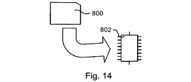
図14は、コンピュータプログラム及びプロセッサを概略的に示している。上の方法は、特にコントローラ340、440がプロセッサ又はプログラマブル回路として実装されるケースについて、コンピュータ及び/又はプロセッサといった処理手段の支援を伴う実装に適している。従って、図13を参照しながら説明した実施形態のいずれかに係る任意の方法のステップを処理手段、プロセッサ又はコンピュータに実行させるように構成される命令を含むコンピュータプログラムが提供される。コンピュータプログラムは、好適には、図14に示したようなコンピュータ読取可能な媒体800に記憶されるプログラムコードを含み、プログラムコードは、処理手段、プロセッサ又はコンピュータ802によってロードされて実行されることができ、好適には、図13を参照しながら説明した実施形態のいずれかの通りに本発明の実施形態に従ってそれぞれ方法を実行させる。コンピュータ802及びコンピュータプログラムプロダクト800は、いずれかの方法のアクションがステップを追って実行されるようにシーケンシャルにプログラムコードを実行するように構成されてもよい。処理手段、プロセッサ又はコンピュータ802は、好適には、通常は組込みシステムとして言及されるものである。よって、図14に描いたコンピュータ読取可能な媒体800及びコンピュータ802は、単に本原理の理解を提供する例示の目的で解釈されるべきであって、要素の何らかの直接的な様子として解釈されるべきではない。
FIG. 14 schematically shows a computer program and a processor. The above method is suitable for implementation with the aid of processing means such as a computer and / or processor, especially for the case where the controllers 340, 440 are implemented as processors or programmable circuits. Accordingly, there is provided a computer program comprising instructions configured to cause a processing means, processor or computer to execute any method steps according to any of the embodiments described with reference to FIG. The computer program preferably includes program code stored on a computer
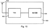
図15は、通信デバイス900を概略的に示すブロック図である。通信デバイス900は、通信ネットワークを介して周波数分割複信で通信可能である。通信デバイス900は、上で詳述した実施形態のいずれかに係る送受信機構成902を備える。送受信機構成902は、そのアンテナポートを通じてアンテナ904へ接続される。当該通信デバイスは、ユーザ向けインタフェース、及び/又は、他の回路若しくはマシン、メモリ、プロセッサなどといった、他の回路群906を備えてもよい。通信デバイス900は、スマートフォン若しくはセルフォン、コンピュータ用の通信カード若しくはデバイス、又はマシン内の組込み通信デバイスなどであってよい。通信デバイス900は、セルラー通信若しくはP2P(point-to-point)通信のために、又は無線若しくは有線ネットワークでの通信のために適合されてもよい。
FIG. 15 is a block diagram schematically showing the
言い換えれば、第1周波数で調整可能なインピーダンスを提供するように構成される電子回路が開示され、当該回路は、上記電子回路の入力端子において入力信号を受け付け、上記入力信号に比例する第1電流信号を提供するように構成される第1相互コンダクタンス増幅器と、第1ミキサ構成、フィルタ構成及び第2ミキサ構成を各々含む少なくとも1つの変換構成であって、上記第1ミキサ構成は、上記第1周波数にあたる第1局部発振器信号を利用して、上記第1電流信号を当該ミキサ構成の出力におけるベースバンド電圧信号へとダウンコンバートするように構成され、上記フィルタ構成は、上記第1ミキサ構成の上記出力に接続され、少なくとも抵抗及びキャパシタを並列に含み、上記第2ミキサ構成は、上記第1周波数にあたる第2局部発振器信号を利用して、上記フィルタ構成に現れる電圧信号を自身の出力におけるアップコンバート済み電圧信号へとアップコンバートするように構成される、上記少なくとも1つの変換構成と、上記アップコンバート済み電圧信号を受け付け、それに比例する第2電流信号を提供し、及び上記第2電流信号を上記電子回路の上記入力端子へとフィードバックする、ように構成される第2相互コンダクタンス増幅器と、を含む。 In other words, an electronic circuit configured to provide an adjustable impedance at a first frequency is disclosed, the circuit accepting an input signal at an input terminal of the electronic circuit and a first current proportional to the input signal. A first transconductance amplifier configured to provide a signal and at least one conversion configuration each including a first mixer configuration, a filter configuration, and a second mixer configuration, wherein the first mixer configuration includes the first mixer configuration The first local oscillator signal corresponding to the frequency is used to downconvert the first current signal to a baseband voltage signal at the output of the mixer configuration, and the filter configuration is the same as that of the first mixer configuration. Connected to the output and including at least a resistor and a capacitor in parallel, the second mixer configuration corresponds to the first frequency The at least one conversion configuration configured to upconvert the voltage signal appearing in the filter configuration to an upconverted voltage signal at its output utilizing a two local oscillator signal; and the upconverted voltage A second transconductance amplifier configured to receive a signal, provide a second current signal proportional thereto, and feed back the second current signal to the input terminal of the electronic circuit.
この手法で上記第1ミキサ構成及び上記第2ミキサ構成を使用することにより、(狭帯域ベースバンドインピーダンスとみなすこともできる)抵抗及びキャパシタと共に実装されるフィルタ構成を、無線周波数へとアップコンバートすることができる。この手法で、高い品質係数に対応するシャープな周波数応答を、品質係数の非常に高いインダクタを必要とすることなく、周波数変換技法を用いて達成することができる。ベースバンドインピーダンスの帯域幅を十分に狭くすることにより、2つ以上の変換後インピーダンス回路を、近傍の周波数にて限られた相互作用と共に使用することができる。 By using the first mixer configuration and the second mixer configuration in this manner, a filter configuration implemented with a resistor and a capacitor (which can be regarded as a narrowband baseband impedance) is upconverted to a radio frequency. be able to. With this approach, a sharp frequency response corresponding to a high quality factor can be achieved using frequency conversion techniques without the need for an inductor with a very high quality factor. By sufficiently narrowing the bandwidth of the baseband impedance, two or more post-conversion impedance circuits can be used with limited interaction at nearby frequencies.
上記第1相互コンダクタンス増幅器及び上記第2相互コンダクタンス増幅器のうちの一方は反転相互コンダクタンス増幅器であってよく、他方は非反転相互コンダクタンス増幅器であってよい。これは、回路の低周波数での安定性を確実化する。 One of the first transconductance amplifier and the second transconductance amplifier may be an inverting transconductance amplifier, and the other may be a non-inverting transconductance amplifier. This ensures the low frequency stability of the circuit.
上記第1相互コンダクタンス増幅器及び上記第2相互コンダクタンス増幅器のうちの少なくとも一方が制御可能な利得を有する場合、提供されるインピーダンスの大きさをその制御可能な相互コンダクタンス増幅器の利得を制御することにより調整することができる。上記フィルタ構成の上記抵抗及び上記キャパシタのうちの少なくとも一方が制御可能である場合、同様の結果を達成することができる。 If at least one of the first transconductance amplifier and the second transconductance amplifier has a controllable gain, the magnitude of the impedance provided is adjusted by controlling the gain of the controllable transconductance amplifier can do. Similar results can be achieved if at least one of the resistor and the capacitor of the filter configuration is controllable.
上記第2局部発振器信号が上記第1局部発振器信号を基準とする位相オフセットを有する場合、インピーダンスに異なる位相角を提供することができる。上記位相オフセットが制御可能である場合、提供されるインピーダンスの位相角もまた制御されることができる。 If the second local oscillator signal has a phase offset relative to the first local oscillator signal, a different phase angle can be provided for the impedance. If the phase offset is controllable, the phase angle of the provided impedance can also be controlled.
上記電子回路は、2つの変換構成の上記第1局部発振器信号が0度とも180度とも異なる位相差を有する当該2つの変換構成を含んでもよい。この手法で、上記回路に、当該回路への入力信号が上記第1局部発振器信号と同じ周波数及び同じ位相を有しない状況において、所望のインピーダンスを提供することもまた可能となる。1つの実施形態において、上記2つの変換構成の上記第1局部発振器信号は、90度に等しい位相差を有する。 The electronic circuit may include the two conversion configurations in which the first local oscillator signal of the two conversion configurations has a phase difference different from both 0 degrees and 180 degrees. In this manner, it is also possible to provide the circuit with a desired impedance in situations where the input signal to the circuit does not have the same frequency and phase as the first local oscillator signal. In one embodiment, the first local oscillator signal of the two conversion configurations has a phase difference equal to 90 degrees.
代替的に、上記電子回路は、変換構成の上記第1局部発振器信号が360度にわたる対称的な位相分配を有する少なくとも3つの変換構成を含んでもよい。1つの実施形態において、上記電子回路は、4つの変換構成を含み、当該4つの変換構成の上記第1局部発振器信号は、直角位相群を有する。 Alternatively, the electronic circuit may include at least three conversion configurations in which the first local oscillator signal of the conversion configuration has a symmetric phase distribution spanning 360 degrees. In one embodiment, the electronic circuit includes four conversion configurations, and the first local oscillator signal of the four conversion configurations has a quadrature group.
名目インピーダンスが上記電子回路の上記入力端子に並列に配置されてもよい。 A nominal impedance may be placed in parallel with the input terminal of the electronic circuit.
ある回路構成は、共通的な入力端子へ接続される上述したような少なくとも2つの電子回路を含んでよく、上記少なくとも2つの電子回路は、異なる周波数にあたる局部発振器信号を利用して、当該異なる周波数の各々において調整可能なインピーダンスを提供する。この手法で、上記回路構成は、送受信機の受信周波数及び送信周波数などといった異なる周波数において異なるインピーダンスを同時に提供することができる。 A circuit configuration may include at least two electronic circuits, as described above, connected to a common input terminal, the at least two electronic circuits utilizing local oscillator signals at different frequencies and using the different frequencies. Each providing an adjustable impedance. In this manner, the circuit configuration can simultaneously provide different impedances at different frequencies, such as the reception and transmission frequencies of the transceiver.
ある送受信機構成は、通信ネットワークとの周波数分割複信での通信のために構成される受信機と、上記通信ネットワークとの周波数分割複信での通信のために構成される送信機と、アンテナへの接続用の送信ポートと、上述したような回路構成を含み、上記送信ポートにおけるインピーダンスを模倣するように構成されるインピーダンス均衡回路と、第1タイプのフィルタ及び第2タイプのフィルタを含み、上記受信機、送信機、送信ポート及びインピーダンス均衡回路を接続するフィルタ構成と、を含んでよく、上記第1タイプのフィルタは、送信機周波数の信号を通過させ及び受信機周波数の信号を減衰させるように構成され、上記送信機と上記送信ポートとの間、及び上記受信機と上記インピーダンス均衡回路との間に接続され、上記第2タイプのフィルタは、送信機周波数の信号を減衰させ及び受信機周波数の信号を通過させるように構成され、上記送信機と上記インピーダンス均衡回路との間、及び上記受信機と上記送信ポートとの間に接続される。 A transceiver configuration includes a receiver configured for communication in frequency division duplex with a communication network, a transmitter configured for communication in frequency division duplex with the communication network, and an antenna. Including a transmission port for connection to, an impedance balancing circuit configured to mimic an impedance at the transmission port, including a circuit configuration as described above, a first type filter and a second type filter, A filter arrangement connecting the receiver, transmitter, transmission port and impedance balancing circuit, wherein the first type of filter passes the signal at the transmitter frequency and attenuates the signal at the receiver frequency. Connected between the transmitter and the transmission port and between the receiver and the impedance balancing circuit, and The second type of filter is configured to attenuate a transmitter frequency signal and pass a receiver frequency signal, between the transmitter and the impedance balancing circuit, and between the receiver and the transmission port. Connected between.
上記送受信機構成は、上記受信機の入力ポートの少なくとも1つの端子において振幅検出器構成をさらに含んでよく、上記送受信機構成は、上記受信機の入力ポートの上記少なくとも1つの端子における振幅が上記振幅検出器構成による測定結果に基づいて低減されるように、上記インピーダンス均衡回路の調整可能なインピーダンスを制御する、ように構成されるコントローラ、を含む。この手法で、上記インピーダンス均衡回路を、アンテナインピーダンスを模倣するように制御することができる。 The transceiver configuration may further include an amplitude detector configuration at at least one terminal of the input port of the receiver, wherein the transceiver configuration has an amplitude at the at least one terminal of the input port of the receiver as described above. A controller configured to control an adjustable impedance of the impedance balance circuit to be reduced based on measurement results from the amplitude detector configuration. In this way, the impedance balancing circuit can be controlled to mimic the antenna impedance.
上記コントローラは、上記第1相互コンダクタンス増幅器の制御可能な利得、上記第2相互コンダクタンス増幅器の制御可能な利得、及び上記フィルタ構成の上記抵抗、のうちの少なくとも1つを制御することにより、上記インピーダンス均衡回路の上記調整可能なインピーダンスの大きさを制御する、ように構成されてもよい。 The controller controls the impedance by controlling at least one of a controllable gain of the first transconductance amplifier, a controllable gain of the second transconductance amplifier, and the resistance of the filter configuration. It may be configured to control the adjustable impedance magnitude of the balanced circuit.
上記コントローラは、上記第1局部発振器信号を基準とする上記第2局部発振器信号の位相オフセットを制御することにより、上記インピーダンス均衡回路の上記調整可能なインピーダンスの位相を制御する、ようにさらに構成されてもよい。 The controller is further configured to control the phase of the adjustable impedance of the impedance balancing circuit by controlling a phase offset of the second local oscillator signal relative to the first local oscillator signal. May be.
通信ネットワークを介して周波数分割複信での通信の可能な通信デバイスは、上述したような送受信機構成を含んでもよい。 A communication device capable of communication by frequency division duplex via a communication network may include a transceiver configuration as described above.
第1周波数において調整可能なインピーダンスを提供する方法は、第1相互コンダクタンス増幅器により、電子回路の入力端子において受け付けた入力信号に比例する第1電流信号を提供するステップと、少なくとも1つの変換構成の第1ミキサ構成において、上記第1周波数にあたる第1局部発振器信号を利用することにより、上記第1電流信号をベースバンド電圧信号へとダウンコンバートするステップと、上記少なくとも1つの変換構成の少なくとも抵抗及びキャパシタを並列に含むフィルタ構成において、上記ベースバンド電圧信号をフィルタリングして、上記フィルタ構成における電圧信号を提供するステップと、上記少なくとも1つの変換構成の第2ミキサ構成において、上記第1周波数にあたる第2局部発振器信号を利用することにより、上記フィルタ構成に現れる上記電圧信号をアップコンバート済み電圧信号へとアップコンバートするステップと、第2相互コンダクタンス増幅器により、上記アップコンバート済み電圧信号に比例する第2電流信号を提供するステップと、上記第2電流信号を上記電子回路の上記入力端子へとフィードバックするステップと、を含む。 A method for providing an adjustable impedance at a first frequency includes providing a first current signal proportional to an input signal received at an input terminal of an electronic circuit with a first transconductance amplifier; and at least one conversion configuration Downconverting the first current signal into a baseband voltage signal by utilizing a first local oscillator signal corresponding to the first frequency in a first mixer configuration; and at least a resistance of the at least one conversion configuration; Filtering a baseband voltage signal to provide a voltage signal in the filter configuration in a filter configuration including a capacitor in parallel; and a second mixer configuration in the at least one conversion configuration in a second mixer configuration corresponding to the first frequency. Use two local oscillator signals And upconverting the voltage signal appearing in the filter configuration to an upconverted voltage signal, and providing a second current signal proportional to the upconverted voltage signal by a second transconductance amplifier. Feeding back the second current signal to the input terminal of the electronic circuit.
この手法で上記第1ミキサ構成及び上記第2ミキサ構成を使用することにより、(狭帯域ベースバンドインピーダンスとみなすこともできる)抵抗及びキャパシタと共に実装されるフィルタ構成を、無線周波数へとアップコンバートすることができる。この手法で、高い品質係数に対応するシャープな周波数応答を、品質係数の非常に高いインダクタを必要とすることなく、周波数変換技法を用いて達成することができる。ベースバンドインピーダンスの帯域幅を十分に狭くすることにより、2つ以上の変換後インピーダンス回路を、近傍の周波数にて限られた相互作用と共に使用することができる。 By using the first mixer configuration and the second mixer configuration in this manner, a filter configuration implemented with a resistor and a capacitor (which can be regarded as a narrowband baseband impedance) is upconverted to a radio frequency. be able to. With this approach, a sharp frequency response corresponding to a high quality factor can be achieved using frequency conversion techniques without the need for an inductor with a very high quality factor. By sufficiently narrowing the bandwidth of the baseband impedance, two or more post-conversion impedance circuits can be used with limited interaction at nearby frequencies.
上記方法は、上記第1相互コンダクタンス増幅器の制御可能な利得、上記第2相互コンダクタンス増幅器の制御可能な利得、及び上記フィルタ構成の上記抵抗、のうちの少なくとも1つを制御することにより、上記調整可能なインピーダンスの大きさを制御するステップ、をさらに含んでもよい。 The method includes controlling the at least one of a controllable gain of the first transconductance amplifier, a controllable gain of the second transconductance amplifier, and the resistance of the filter configuration. The method may further include the step of controlling the magnitude of possible impedance.
上記方法は、上記第1局部発振器信号を基準とする上記第2局部発振器信号の位相オフセットを制御することにより、上記調整可能なインピーダンスの位相を制御するステップ、をさらに含んでもよい。 The method may further include controlling the phase of the adjustable impedance by controlling a phase offset of the second local oscillator signal relative to the first local oscillator signal.
本発明の多様な実施形態が説明され及び図示されたが、本発明はそれらに限定されず、次の特許請求の範囲において定義される主題の範囲内で、他の形で具現化されてもよい。
While various embodiments of the invention have been described and illustrated, the invention is not so limited and may be embodied in other forms within the scope of the subject matter defined in the following claims. Good.
Claims (15)
前記電子回路の入力端子において入力信号を受け付け、前記入力信号に比例する第1電流信号を提供するように構成される第1相互コンダクタンス増幅器(52)と、
第1ミキサ構成(53;63;73;83)、フィルタ構成(54,55;64,65;74,75;84,85)及び第2ミキサ構成(56;66;76;86)を各々含む少なくとも1つの変換構成であって、
前記第1ミキサ構成は、前記第1周波数にあたる第1局部発振器信号を利用して、前記第1電流信号を当該ミキサ構成の出力におけるベースバンド電圧信号へとダウンコンバートするように構成され、
前記フィルタ構成は、前記第1ミキサ構成(53;63;73;83)の前記出力に接続され、少なくとも抵抗及びキャパシタを並列に含み、
前記第2ミキサ構成は、前記第1周波数にあたる第2局部発振器信号を利用して、前記フィルタ構成に現れる電圧信号を自身の出力におけるアップコンバート済み電圧信号へとアップコンバートするように構成される、
前記少なくとも1つの変換構成と、
前記アップコンバート済み電圧信号を受け付け、それに比例する第2電流信号を提供し、及び前記第2電流信号を前記電子回路の前記入力端子へとフィードバックする、ように構成される第2相互コンダクタンス増幅器(57)と、
を含む電子回路。 An electronic circuit (51; 61; 71; 81) configured to provide an adjustable impedance at a first frequency comprising:
A first transconductance amplifier (52) configured to accept an input signal at an input terminal of the electronic circuit and provide a first current signal proportional to the input signal;
Each includes a first mixer configuration (53; 63; 73; 83), a filter configuration (54, 55; 64, 65; 74, 75; 84, 85) and a second mixer configuration (56; 66; 76; 86). At least one conversion configuration,
The first mixer configuration is configured to downconvert the first current signal to a baseband voltage signal at the output of the mixer configuration using a first local oscillator signal corresponding to the first frequency,
The filter configuration is connected to the output of the first mixer configuration (53; 63; 73; 83) and includes at least a resistor and a capacitor in parallel;
The second mixer configuration is configured to upconvert a voltage signal appearing in the filter configuration to an upconverted voltage signal at its output utilizing a second local oscillator signal corresponding to the first frequency.
The at least one conversion configuration;
A second transconductance amplifier configured to receive the upconverted voltage signal, provide a second current signal proportional thereto, and feed back the second current signal to the input terminal of the electronic circuit; 57)
Including electronic circuit.
前記少なくとも2つの電子回路(92,93)は、異なる周波数にあたる局部発振器信号を利用して、当該異なる周波数の各々において調整可能なインピーダンスを提供する、
回路構成。 A circuit configuration (91) comprising at least two electronic circuits (92, 93) according to any one of claims 1 to 11, connected to a common input terminal,
The at least two electronic circuits (92, 93) utilize local oscillator signals at different frequencies to provide adjustable impedance at each of the different frequencies;
Circuit configuration.
前記通信ネットワークとの周波数分割複信での通信のために構成される送信機(32)と、
アンテナへの接続用の送信ポート(34)と、
請求項12に記載の回路構成を含み、前記送信ポートにおけるインピーダンスを模倣するように構成されるインピーダンス均衡回路(35)と、
第1タイプのフィルタ(36,37)及び第2タイプのフィルタ(38,39)を含み、前記受信機(33)、送信機(32)、送信ポート(34)及びインピーダンス均衡回路(35)を接続するフィルタ構成と、
を含み、
前記第1タイプのフィルタ(36,37)は、送信機周波数の信号を通過させ及び受信機周波数の信号を減衰させるように構成され、前記送信機(32)と前記送信ポート(34)との間、及び前記受信機(33)と前記インピーダンス均衡回路(35)との間に接続され、
前記第2タイプのフィルタ(38,39)は、送信機周波数の信号を減衰させ及び受信機周波数の信号を通過させるように構成され、前記送信機(32)と前記インピーダンス均衡回路(35)との間、及び前記受信機(33)と前記送信ポート(34)との間に接続される、
送受信機構成(95,902)。 A receiver (33) configured for communication in frequency division duplex with a communication network;
A transmitter (32) configured for communication in frequency division duplex with the communication network;
A transmission port (34) for connection to the antenna;
An impedance balancing circuit (35) comprising the circuitry of claim 12 and configured to mimic the impedance at the transmission port;
Including a first type filter (36, 37) and a second type filter (38, 39), the receiver (33), transmitter (32), transmission port (34) and impedance balance circuit (35). The filter configuration to connect,
Including
The first type filter (36, 37) is configured to pass a signal of a transmitter frequency and attenuate a signal of a receiver frequency, and the filter of the transmitter (32) and the transmission port (34). And between the receiver (33) and the impedance balancing circuit (35),
The second type filter (38, 39) is configured to attenuate a transmitter frequency signal and pass a receiver frequency signal, the transmitter (32), the impedance balance circuit (35), And between the receiver (33) and the transmission port (34),
Transceiver configuration (95, 902).
第1相互コンダクタンス増幅器により、電子回路の入力端子において受け付けた入力信号に比例する第1電流信号を提供するステップ(101)と、
少なくとも1つの変換構成の第1ミキサ構成において、前記第1周波数にあたる第1局部発振器信号を利用することにより、前記第1電流信号をベースバンド電圧信号へとダウンコンバートするステップ(102)と、
前記少なくとも1つの変換構成の少なくとも抵抗及びキャパシタを並列に含むフィルタ構成において、前記ベースバンド電圧信号をフィルタリングして、前記フィルタ構成における電圧信号を提供するステップ(103)と、
前記少なくとも1つの変換構成の第2ミキサ構成において、前記第1周波数にあたる第2局部発振器信号を利用することにより、前記フィルタ構成に現れる前記電圧信号をアップコンバート済み電圧信号へとアップコンバートするステップ(104)と、
第2相互コンダクタンス増幅器により、前記アップコンバート済み電圧信号に比例する第2電流信号を提供するステップ(105)と、
前記第2電流信号を前記電子回路の前記入力端子へとフィードバックするステップ(106)と、
を含む方法。 A method for providing an adjustable impedance at a first frequency comprising:
Providing a first current signal proportional to an input signal received at an input terminal of the electronic circuit by a first transconductance amplifier;
Downconverting the first current signal to a baseband voltage signal by utilizing a first local oscillator signal corresponding to the first frequency in a first mixer configuration of at least one conversion configuration; and
Filtering the baseband voltage signal to provide a voltage signal in the filter configuration in a filter configuration including in parallel at least a resistor and a capacitor of the at least one conversion configuration;
Upconverting the voltage signal appearing in the filter configuration into an upconverted voltage signal by utilizing a second local oscillator signal corresponding to the first frequency in the second mixer configuration of the at least one conversion configuration ( 104)
Providing a second current signal proportional to the upconverted voltage signal by a second transconductance amplifier (105);
Feeding back the second current signal to the input terminal of the electronic circuit (106);
Including methods.
Applications Claiming Priority (1)
| Application Number | Priority Date | Filing Date | Title |
|---|---|---|---|
| PCT/EP2014/053371 WO2015124195A1 (en) | 2014-02-20 | 2014-02-20 | Circuit and method for providing an adjustable impedance |
Publications (2)
| Publication Number | Publication Date |
|---|---|
| JP2017511042A JP2017511042A (en) | 2017-04-13 |
| JP6251414B2 true JP6251414B2 (en) | 2017-12-20 |
Family
ID=50239588
Family Applications (1)
| Application Number | Title | Priority Date | Filing Date |
|---|---|---|---|
| JP2016553469A Active JP6251414B2 (en) | 2014-02-20 | 2014-02-20 | Circuit and method for providing adjustable impedance |
Country Status (5)
| Country | Link |
|---|---|
| US (1) | US10079671B2 (en) |
| EP (1) | EP3108587B1 (en) |
| JP (1) | JP6251414B2 (en) |
| IL (1) | IL247059B (en) |
| WO (1) | WO2015124195A1 (en) |
Families Citing this family (9)
| Publication number | Priority date | Publication date | Assignee | Title |
|---|---|---|---|---|
| WO2015049012A1 (en) * | 2013-10-04 | 2015-04-09 | Telefonaktiebolaget L M Ericsson (Publ) | Transceiver arrangement, communication device, and method |
| CN108352853B (en) * | 2015-11-04 | 2020-07-31 | 株式会社村田制作所 | Wave splitting device and design method thereof |
| US11063570B2 (en) * | 2017-02-10 | 2021-07-13 | Telefonaktiebolaget Lm Ericsson (Publ) | Integrated isolator circuit in a time division duplex transceiver |
| JP2018198372A (en) * | 2017-05-23 | 2018-12-13 | 京セラ株式会社 | Electronic apparatus |
| FR3084548B1 (en) * | 2018-07-26 | 2020-10-02 | Univ Bordeaux | RADIOFREQUENCY RECEPTION AND / OR TRANSMISSION CHAIN AND ASSOCIATED PROCESS |
| EP3716493B1 (en) * | 2019-03-29 | 2021-11-10 | Nokia Solutions and Networks Oy | Full duplex transmission arrangement |
| WO2020243949A1 (en) * | 2019-06-06 | 2020-12-10 | 华为技术有限公司 | Filter and circuit for transmitting channel |
| CN112947182B (en) * | 2021-02-05 | 2023-05-26 | 电子科技大学 | Control circuit for improving common mode transient anti-interference degree of negative transconductance oscillator |
| US20220376731A1 (en) * | 2021-05-19 | 2022-11-24 | Qualcomm Incorporated | System and method for sharing circuitry between transmit and receive path |
Family Cites Families (15)
| Publication number | Priority date | Publication date | Assignee | Title |
|---|---|---|---|---|
| GB9910454D0 (en) * | 1999-05-07 | 1999-07-07 | Koninkl Philips Electronics Nv | Circuit arrangement providing impedance translation filtering |
| GB2365235B (en) * | 2000-07-20 | 2004-07-21 | British Broadcasting Corp | A circuit for simulating an impedance |
| US6549074B2 (en) * | 2000-12-05 | 2003-04-15 | Nippon Telegraph And Telephone Corporation | Transconductance amplifier, filter using the transconductance amplifier and tuning circuitry for transconductance amplifier in the filter |
| JP4588786B2 (en) * | 2006-02-28 | 2010-12-01 | 富士通株式会社 | Clock divider circuit |
| US7949322B2 (en) * | 2007-03-09 | 2011-05-24 | Qualcomm, Incorporated | Frequency selective amplifier with wide-band impedance and noise matching |
| US8526903B2 (en) * | 2008-03-11 | 2013-09-03 | Qualcomm, Incorporated | High-linearity receiver with transmit leakage cancellation |
| US8208866B2 (en) * | 2008-08-05 | 2012-06-26 | Broadcom Corporation | RF transceiver front-end with RX/TX isolation |
| US8285241B2 (en) * | 2009-07-30 | 2012-10-09 | Broadcom Corporation | Receiver apparatus having filters implemented using frequency translation techniques |
| US8208865B2 (en) | 2009-09-11 | 2012-06-26 | Broadcom Corporation | RF front-end with on-chip transmitter/receiver isolation and noise-matched LNA |
| CN102577106B (en) * | 2009-09-22 | 2015-04-15 | 诺基亚公司 | Adjustable circuit architecture |
| US8725085B2 (en) | 2010-06-03 | 2014-05-13 | Broadcom Corporation | RF front-end module |
| US9083441B2 (en) * | 2011-10-26 | 2015-07-14 | Qualcomm Incorporated | Impedance balancing for transmitter to receiver rejection |
| EP2587679B1 (en) * | 2011-10-27 | 2015-01-07 | Nxp B.V. | Rf receiver with voltage sampling |
| US9214918B2 (en) * | 2012-03-14 | 2015-12-15 | Broadcom Corporation | Power distributing duplexer system |
| EP2672631B1 (en) * | 2012-06-07 | 2014-12-24 | Telefonaktiebolaget L M Ericsson (publ) | Duplexer-less transceiver and communication apparatus |
-
2014
- 2014-02-20 EP EP14708816.5A patent/EP3108587B1/en active Active
- 2014-02-20 JP JP2016553469A patent/JP6251414B2/en active Active
- 2014-02-20 US US15/117,219 patent/US10079671B2/en active Active
- 2014-02-20 WO PCT/EP2014/053371 patent/WO2015124195A1/en active Application Filing
-
2016
- 2016-08-02 IL IL247059A patent/IL247059B/en active IP Right Grant
Also Published As
| Publication number | Publication date |
|---|---|
| WO2015124195A1 (en) | 2015-08-27 |
| US10079671B2 (en) | 2018-09-18 |
| EP3108587A1 (en) | 2016-12-28 |
| IL247059B (en) | 2018-12-31 |
| US20160352496A1 (en) | 2016-12-01 |
| EP3108587B1 (en) | 2017-07-26 |
| JP2017511042A (en) | 2017-04-13 |
Similar Documents
| Publication | Publication Date | Title |
|---|---|---|
| JP6251414B2 (en) | Circuit and method for providing adjustable impedance | |
| US9793943B2 (en) | Duplexer-less transceiver and communication apparatus | |
| US10348356B2 (en) | Transmitter receiver leakage reduction in a full duplex system without the use of a duplexer | |
| US9871552B2 (en) | Transceiver arrangement, communication device, method and computer program | |
| US10027465B2 (en) | Transceiver arrangement, communication device, method and computer program | |
| US9900044B2 (en) | Transceiver arrangement and communication device | |
| JP6552832B2 (en) | Redundant apparatus, wireless device, and related method | |
| US9853801B2 (en) | Transceiver arrangement, communication device, and method | |
| TWI517601B (en) | Transmission arrangement and method for analyzing an amplified transmission signal | |
| JP6728193B2 (en) | Circuit and method for transceiver self-interference canceller | |
| Agrawal et al. | Multi-band RF time delay element based on frequency translation |
Legal Events
| Date | Code | Title | Description |
|---|---|---|---|
| A977 | Report on retrieval |
Free format text: JAPANESE INTERMEDIATE CODE: A971007 Effective date: 20171018 |
|
| TRDD | Decision of grant or rejection written | ||
| A01 | Written decision to grant a patent or to grant a registration (utility model) |
Free format text: JAPANESE INTERMEDIATE CODE: A01 Effective date: 20171024 |
|
| A61 | First payment of annual fees (during grant procedure) |
Free format text: JAPANESE INTERMEDIATE CODE: A61 Effective date: 20171124 |
|
| R150 | Certificate of patent or registration of utility model |
Ref document number: 6251414 Country of ref document: JP Free format text: JAPANESE INTERMEDIATE CODE: R150 |
|
| R250 | Receipt of annual fees |
Free format text: JAPANESE INTERMEDIATE CODE: R250 |
|
| R250 | Receipt of annual fees |
Free format text: JAPANESE INTERMEDIATE CODE: R250 |
|
| R250 | Receipt of annual fees |
Free format text: JAPANESE INTERMEDIATE CODE: R250 |
|
| R250 | Receipt of annual fees |
Free format text: JAPANESE INTERMEDIATE CODE: R250 |