JP6239595B2 - Method for measuring beam position in a multi beam exposure apparatus and method for measuring the distance between two beam beams - Google Patents
Method for measuring beam position in a multi beam exposure apparatus and method for measuring the distance between two beam beams Download PDFInfo
- Publication number
- JP6239595B2 JP6239595B2 JP2015512021A JP2015512021A JP6239595B2 JP 6239595 B2 JP6239595 B2 JP 6239595B2 JP 2015512021 A JP2015512021 A JP 2015512021A JP 2015512021 A JP2015512021 A JP 2015512021A JP 6239595 B2 JP6239595 B2 JP 6239595B2
- Authority
- JP
- Japan
- Prior art keywords
- charged particle
- blocking
- dimensional
- dimensional pattern
- feature
- Prior art date
- Legal status (The legal status is an assumption and is not a legal conclusion. Google has not performed a legal analysis and makes no representation as to the accuracy of the status listed.)
- Active
Links
- 238000000034 method Methods 0.000 title claims description 64
- 239000002245 particle Substances 0.000 claims description 103
- 230000000903 blocking effect Effects 0.000 claims description 85
- 238000005259 measurement Methods 0.000 claims description 73
- 238000006243 chemical reaction Methods 0.000 claims description 33
- 230000004044 response Effects 0.000 claims description 9
- 239000010410 layer Substances 0.000 description 21
- 238000010894 electron beam technology Methods 0.000 description 15
- 238000001459 lithography Methods 0.000 description 15
- 238000010586 diagram Methods 0.000 description 10
- JNDMLEXHDPKVFC-UHFFFAOYSA-N aluminum;oxygen(2-);yttrium(3+) Chemical compound [O-2].[O-2].[O-2].[Al+3].[Y+3] JNDMLEXHDPKVFC-UHFFFAOYSA-N 0.000 description 8
- 229910019901 yttrium aluminum garnet Inorganic materials 0.000 description 8
- 239000000463 material Substances 0.000 description 5
- 239000000758 substrate Substances 0.000 description 5
- 230000004888 barrier function Effects 0.000 description 4
- 230000003287 optical effect Effects 0.000 description 4
- 230000008901 benefit Effects 0.000 description 3
- 239000011248 coating agent Substances 0.000 description 3
- 238000000576 coating method Methods 0.000 description 3
- 238000012937 correction Methods 0.000 description 3
- 238000013461 design Methods 0.000 description 3
- 238000004519 manufacturing process Methods 0.000 description 3
- 238000000691 measurement method Methods 0.000 description 3
- 229910052751 metal Inorganic materials 0.000 description 3
- 239000002184 metal Substances 0.000 description 3
- 239000013307 optical fiber Substances 0.000 description 3
- 238000000059 patterning Methods 0.000 description 3
- 230000007704 transition Effects 0.000 description 3
- 238000004364 calculation method Methods 0.000 description 2
- 230000008859 change Effects 0.000 description 2
- 239000011247 coating layer Substances 0.000 description 2
- 238000000609 electron-beam lithography Methods 0.000 description 2
- 230000008569 process Effects 0.000 description 2
- 230000009467 reduction Effects 0.000 description 2
- 239000004065 semiconductor Substances 0.000 description 2
- WFKWXMTUELFFGS-UHFFFAOYSA-N tungsten Chemical compound [W] WFKWXMTUELFFGS-UHFFFAOYSA-N 0.000 description 2
- 229910052721 tungsten Inorganic materials 0.000 description 2
- 239000010937 tungsten Substances 0.000 description 2
- VYZAMTAEIAYCRO-UHFFFAOYSA-N Chromium Chemical compound [Cr] VYZAMTAEIAYCRO-UHFFFAOYSA-N 0.000 description 1
- RTAQQCXQSZGOHL-UHFFFAOYSA-N Titanium Chemical compound [Ti] RTAQQCXQSZGOHL-UHFFFAOYSA-N 0.000 description 1
- 229910052782 aluminium Inorganic materials 0.000 description 1
- XAGFODPZIPBFFR-UHFFFAOYSA-N aluminium Chemical compound [Al] XAGFODPZIPBFFR-UHFFFAOYSA-N 0.000 description 1
- 238000004458 analytical method Methods 0.000 description 1
- 238000013459 approach Methods 0.000 description 1
- 230000009286 beneficial effect Effects 0.000 description 1
- 230000005540 biological transmission Effects 0.000 description 1
- 229910052804 chromium Inorganic materials 0.000 description 1
- 239000011651 chromium Substances 0.000 description 1
- 230000000295 complement effect Effects 0.000 description 1
- 238000005137 deposition process Methods 0.000 description 1
- 238000001514 detection method Methods 0.000 description 1
- 230000005684 electric field Effects 0.000 description 1
- 238000005516 engineering process Methods 0.000 description 1
- 238000005530 etching Methods 0.000 description 1
- 229910044991 metal oxide Inorganic materials 0.000 description 1
- 150000004706 metal oxides Chemical class 0.000 description 1
- 238000012986 modification Methods 0.000 description 1
- 230000004048 modification Effects 0.000 description 1
- 238000012545 processing Methods 0.000 description 1
- 230000005855 radiation Effects 0.000 description 1
- 230000035945 sensitivity Effects 0.000 description 1
- 239000010936 titanium Substances 0.000 description 1
- 229910052719 titanium Inorganic materials 0.000 description 1
- 238000012546 transfer Methods 0.000 description 1
- 238000011144 upstream manufacturing Methods 0.000 description 1
Images


Classifications
-
- B—PERFORMING OPERATIONS; TRANSPORTING
- B82—NANOTECHNOLOGY
- B82Y—SPECIFIC USES OR APPLICATIONS OF NANOSTRUCTURES; MEASUREMENT OR ANALYSIS OF NANOSTRUCTURES; MANUFACTURE OR TREATMENT OF NANOSTRUCTURES
- B82Y10/00—Nanotechnology for information processing, storage or transmission, e.g. quantum computing or single electron logic
-
- B—PERFORMING OPERATIONS; TRANSPORTING
- B82—NANOTECHNOLOGY
- B82Y—SPECIFIC USES OR APPLICATIONS OF NANOSTRUCTURES; MEASUREMENT OR ANALYSIS OF NANOSTRUCTURES; MANUFACTURE OR TREATMENT OF NANOSTRUCTURES
- B82Y40/00—Manufacture or treatment of nanostructures
-
- G—PHYSICS
- G01—MEASURING; TESTING
- G01B—MEASURING LENGTH, THICKNESS OR SIMILAR LINEAR DIMENSIONS; MEASURING ANGLES; MEASURING AREAS; MEASURING IRREGULARITIES OF SURFACES OR CONTOURS
- G01B11/00—Measuring arrangements characterised by the use of optical techniques
- G01B11/14—Measuring arrangements characterised by the use of optical techniques for measuring distance or clearance between spaced objects or spaced apertures
-
- H—ELECTRICITY
- H01—ELECTRIC ELEMENTS
- H01J—ELECTRIC DISCHARGE TUBES OR DISCHARGE LAMPS
- H01J37/00—Discharge tubes with provision for introducing objects or material to be exposed to the discharge, e.g. for the purpose of examination or processing thereof
- H01J37/30—Electron-beam or ion-beam tubes for localised treatment of objects
- H01J37/304—Controlling tubes by information coming from the objects or from the beam, e.g. correction signals
- H01J37/3045—Object or beam position registration
-
- H—ELECTRICITY
- H01—ELECTRIC ELEMENTS
- H01J—ELECTRIC DISCHARGE TUBES OR DISCHARGE LAMPS
- H01J37/00—Discharge tubes with provision for introducing objects or material to be exposed to the discharge, e.g. for the purpose of examination or processing thereof
- H01J37/30—Electron-beam or ion-beam tubes for localised treatment of objects
- H01J37/317—Electron-beam or ion-beam tubes for localised treatment of objects for changing properties of the objects or for applying thin layers thereon, e.g. for ion implantation
- H01J37/3174—Particle-beam lithography, e.g. electron beam lithography
- H01J37/3177—Multi-beam, e.g. fly's eye, comb probe
-
- H—ELECTRICITY
- H01—ELECTRIC ELEMENTS
- H01J—ELECTRIC DISCHARGE TUBES OR DISCHARGE LAMPS
- H01J2237/00—Discharge tubes exposing object to beam, e.g. for analysis treatment, etching, imaging
- H01J2237/06—Sources
- H01J2237/065—Source emittance characteristics
-
- H—ELECTRICITY
- H01—ELECTRIC ELEMENTS
- H01J—ELECTRIC DISCHARGE TUBES OR DISCHARGE LAMPS
- H01J2237/00—Discharge tubes exposing object to beam, e.g. for analysis treatment, etching, imaging
- H01J2237/245—Detection characterised by the variable being measured
- H01J2237/24507—Intensity, dose or other characteristics of particle beams or electromagnetic radiation
- H01J2237/24514—Beam diagnostics including control of the parameter or property diagnosed
-
- H—ELECTRICITY
- H01—ELECTRIC ELEMENTS
- H01J—ELECTRIC DISCHARGE TUBES OR DISCHARGE LAMPS
- H01J2237/00—Discharge tubes exposing object to beam, e.g. for analysis treatment, etching, imaging
- H01J2237/245—Detection characterised by the variable being measured
- H01J2237/24571—Measurements of non-electric or non-magnetic variables
- H01J2237/24578—Spatial variables, e.g. position, distance
-
- H—ELECTRICITY
- H01—ELECTRIC ELEMENTS
- H01J—ELECTRIC DISCHARGE TUBES OR DISCHARGE LAMPS
- H01J2237/00—Discharge tubes exposing object to beam, e.g. for analysis treatment, etching, imaging
- H01J2237/30—Electron or ion beam tubes for processing objects
- H01J2237/317—Processing objects on a microscale
- H01J2237/3175—Lithography
- H01J2237/31774—Multi-beam
Landscapes
- Chemical & Material Sciences (AREA)
- Engineering & Computer Science (AREA)
- Nanotechnology (AREA)
- Analytical Chemistry (AREA)
- Physics & Mathematics (AREA)
- Crystallography & Structural Chemistry (AREA)
- General Physics & Mathematics (AREA)
- Mathematical Physics (AREA)
- Theoretical Computer Science (AREA)
- Manufacturing & Machinery (AREA)
- Condensed Matter Physics & Semiconductors (AREA)
- Electron Beam Exposure (AREA)
- Photometry And Measurement Of Optical Pulse Characteristics (AREA)
Description
本発明は、荷電粒子マルチ小ビーム露光装置において小ビーム位置を測定するための方法に関する。本発明は、さらに、荷電粒子マルチ小ビーム露光装置において2つの小ビーム間の距離を測定するための方法に関する。最後に、本発明は、プロセッサによって実行されるとき、上述の方法のいずれかを行うためのコンピュータ読取可能媒体に関する。 The present invention relates to a method for measuring a beam position in a charged particle multi beam exposure apparatus. The invention further relates to a method for measuring the distance between two beamlets in a charged particle multi-beamlet exposure apparatus. Finally, the invention relates to a computer readable medium for performing any of the methods described above when executed by a processor.
ターゲット面上にパターンを転写するために、ターゲット面上の小ビームの移動と組み合わせた小ビームの制御可能な遮断が、変調情報に従って行われる。マルチ荷電粒子小ビームリソグラフィシステムの一例は、米国特許第6,958,804号に説明され、その開示内容が参照としてここに組み込まれる。 In order to transfer the pattern onto the target surface, a controllable blocking of the beamlets in combination with the movement of the beamlets on the target surface is performed according to the modulation information. An example of a multi-charged particle beamlet lithography system is described in US Pat. No. 6,958,804, the disclosure of which is incorporated herein by reference.
このようなリソグラフィシステムは、非常に多くの、すなわち約10,000以上のオーダ、例えば13,000の小ビームを含むことができる。将来的な設計は、およそ1,000,000の数の小ビームを思い描いている。現在の電子ビームリソグラフィシステムにとって、高解像度でターゲット面をパターニングすることができるようになることが全般的な目標であり、いくつかの用途では、100nm未満のフィーチャサイズの限界寸法のパターンを描画することが可能である。 Such a lithographic system can include a large number of beamlets, ie on the order of about 10,000 or more, for example 13,000. Future designs envision approximately 1,000,000 small beams. It is a general goal for current electron beam lithography systems to be able to pattern target surfaces with high resolution, and for some applications, draw critical dimension patterns of feature sizes below 100 nm. It is possible.
このようなマルチ小ビームに関して、商業的利益が得られる高解像度リソグラフィシステムは、許容エラーが低い必要がある。それ故、荷電粒子小ビームの各々の位置が正確に知られ制御されることが重要である。しかしながら、製造公差及び熱ドリフトなどのさまざまな状況に起因して、このような位置はこれらの予期される所望の位置からずれ、正確なパターニングをできなくする小ビームのずれを起こしうる。 For such multi-beamlets, high resolution lithography systems that provide commercial benefits need to have low tolerance errors. It is therefore important that the position of each charged particle beam is accurately known and controlled. However, due to various circumstances such as manufacturing tolerances and thermal drift, such positions can deviate from these expected desired positions and cause small beam deviations that prevent accurate patterning.
従来のリソグラフィシステムでは、各小ビームの位置は、小ビーム位置の頻繁な測定によって測定される。小ビーム位置の情報を用いて、小ビームが正確な位置にシフトされることができる。 In conventional lithography systems, the position of each beamlet is measured by frequent measurement of beamlet positions. With the information on the beam position, the beam can be shifted to the correct position.
既知の小ビーム位置較正方法は、一般的に、少なくとも3つの工程、すなわち、小ビームの位置が測定される測定工程と、小ビームの測定された位置がその小ビームの所望の予期される位置と比較される計算工程と、測定された位置と所望の位置との差が補正される補正工程とを含む。補正は、リソグラフィシステムのソフトウェア又はハードウェアで行われることができる。 Known beamlet position calibration methods generally involve at least three steps: a measurement step in which the beam position is measured, and the beam beam measured position is the desired expected position of the beam. And a correction step in which the difference between the measured position and the desired position is corrected. The correction can be done in the lithography system software or hardware.
リソグラフィシステムの動作中、ターゲット面のパターニングの精度を改良するために初期位置の較正を可能にするために、小ビーム位置を測定することが望ましい。スループット、すなわち所定時間内にパターニングされることができるターゲット面の数に与える負の影響を制限するために、精度を犠牲にすることなく、限られた時間内に荷電粒子小ビームの位置を測定する方法が実行されることができることが望ましい。 During operation of the lithographic system, it is desirable to measure the beamlet position to allow calibration of the initial position to improve the patterning accuracy of the target surface. Measure the position of a charged particle beamlet within a limited time without sacrificing accuracy to limit the negative impact on throughput, ie the number of target surfaces that can be patterned in a given time It is desirable that the method to be able to be performed.
特に、スループットの損失のなく、小さな寸法に関する産業上増加し続ける要求を考慮すると、リソグラフィシステムにおいて、特に高スループットを提供することを目指している多数の荷電粒子小ビームを含むリソグラフィマシンにおいて、小ビーム特性の測定のためのより正確な装置や技術を提供する必要がある。より高い精度は、リソグラフィマシンの解像度を増加させるために有効である。 In particular, considering the industry's ever-increasing demand for small dimensions without loss of throughput, small beams in lithography systems, especially in lithography machines that include a large number of charged particle beamlets that aim to provide high throughput. There is a need to provide more accurate equipment and techniques for measuring properties. Higher accuracy is effective to increase the resolution of the lithography machine.
特に、スティッチングを使用するとき、例えば描画の失敗を補正するために、2つのビームがウェーハの同じ領域に描画することが好ましい。この技術のために、ナノメートル精度でビーム間隔を知る必要がある。 In particular, when using stitching, it is preferred that the two beams be drawn on the same area of the wafer, for example to correct a writing failure. For this technology, it is necessary to know the beam spacing with nanometer accuracy.
さらに、小ビームの絶対位置がわかっている必要がある。特に、絶対位置のこのような情報は、オーバーレイの精度を、すなわち、既に露光された、あるいはパターニングされた層に対して同じ層内で複数のプロセスによって与えられる連続する層又はフィーチャのアライメント精度の測定を改良することが好ましい。 Furthermore, the absolute position of the small beam needs to be known. In particular, such information of absolute position provides an indication of overlay accuracy, i.e., alignment accuracy of successive layers or features provided by multiple processes within the same layer relative to an already exposed or patterned layer. It is preferred to improve the measurement.
米国特許出願第2007/0057204号は、荷電粒子ビームの位置を測定するための方法を説明している。この方法では、複数の荷電粒子ビーム内の各荷電粒子ビームの位置が、荷電粒子ビームを光ビームに変換するためのコンバータと、光子受光器とを使用して測定される。適宜、遮断要素が、コンバータの表面に設けられる。 US Patent Application No. 2007/0057204 describes a method for measuring the position of a charged particle beam. In this method, the position of each charged particle beam within a plurality of charged particle beams is measured using a converter for converting the charged particle beam into a light beam and a photon receiver. If appropriate, a blocking element is provided on the surface of the converter.
国際出願第2012/062931号公報は、マルチ小ビーム露光装置において2つの小ビーム間の距離を測定するための方法を説明している。この方法では、小ビーム遮断領域と非遮断領域との2次元パターンが設けられたセンサ表面領域が設けられたコンバータが使用されている。 International application 2012/062931 describes a method for measuring the distance between two small beams in a multi-small beam exposure apparatus. In this method, a converter provided with a sensor surface area provided with a two-dimensional pattern of a small beam blocking area and a non-blocking area is used.
上述の特許文献で使用される技術は、衝突する荷電粒子小ビームに関連付けられた光出力の分析に基づいている。走査が行われると、遮断領域から非遮断領域に向かって、又はその逆に荷電粒子小ビームを移動させた結果としての光出力の変化が分析される。 The technique used in the above mentioned patent literature is based on the analysis of the light output associated with the colliding charged particle beam. When the scan is performed, the change in light output as a result of moving the charged particle beam from the blocked area to the non-blocked area or vice versa is analyzed.
多くの用途にとって非常に有用であるが、この技術の精度は、コンバータ面上の遮断フィーチャ、遮断/非遮断パターン、すなわちフィーチャサイズの寸法と比較した小ビームのスポットサイズによって決まる。スポットサイズがフィーチャサイズよりもかなり小さければ、小ビームの正確な位置を見つけるには時間がかかる。一方、小ビームのスポットサイズがフィーチャサイズと比較して大きいと、測定結果をフィッティングするのが難しいので位置を見つけるのが難しい。 Although very useful for many applications, the accuracy of this technique depends on the blocking feature on the converter surface, the blocking / non-blocking pattern, ie the spot size of the beam compared to the feature size dimension. If the spot size is much smaller than the feature size, it will take time to find the exact position of the beam. On the other hand, if the spot size of the small beam is larger than the feature size, it is difficult to fit the measurement result, and thus it is difficult to find the position.
本発明の目的は、リソグラフィシステムなどのマルチ小ビーム露光装置における2つの小ビーム間のビーム間隔測定の精度を改良することに関する。この目的のために、本発明は、荷電粒子マルチ小ビーム露光装置において2つの荷電粒子小ビーム間の距離を測定するための方法であって、前記荷電粒子マルチ小ビーム露光装置には、荷電粒子のエネルギを光に変換するための変換素子と、光感応検出器とを有するセンサが設けられ、前記変換素子には、小ビーム遮断領域と非遮断領域との2次元パターンが設けられたセンサ表面領域が設けられ、この方法は、複数の測定をすることを具備し、各測定は、荷電粒子小ビームで前記2次元パターンの一部分上にフィーチャを露光することを含み、前記フィーチャが露光される位置は、各測定で異なり、複数の位置が2次元グリッドを形成し、2次元パターンの前記非遮断領域を透過された前記露光されたフィーチャの一部である荷電粒子に応答して前記変換素子によって発生された光を受光することと、前記光感応検出器によって受光された光を光強度値に変換して、測定がされた位置に前記光強度値を割り当てることとを含み、この方法は、前記2次元グリッド内のさまざまな位置で前記光強度値によって生成された2次元画像に基づいて前記2次元パターンに対する前記荷電粒子小ビームの位置を測定することを具備する。荷電粒子小ビームのスポットサイズを使用することに代わって2次元パターンの一部分上にフィーチャを露光することは、測定のための最適なフィーチャや2次元パターンを手近にデザインする可能性を開く。これは、測定の順応性をかなり改良し、測定の精度を維持するか、測定の精度を改良する場合もある。 The object of the present invention relates to improving the accuracy of beam spacing measurement between two beamlets in a multi beamlet exposure apparatus such as a lithography system. To this end, the present invention is a method for measuring the distance between two charged particle beamlets in a charged particle multi beamlet exposure apparatus, wherein the charged particle multi beamlet exposure device comprises charged particles. A sensor having a conversion element for converting the energy of the light into light and a photosensitive detector is provided, and the conversion element is provided with a two-dimensional pattern of a small beam blocking area and a non-blocking area. An area is provided, the method comprising making a plurality of measurements, each measurement comprising exposing a feature on a portion of the two-dimensional pattern with a charged particle beam, wherein the feature is exposed The position is different for each measurement, and a plurality of positions form a two-dimensional grid and respond to charged particles that are part of the exposed features that are transmitted through the unblocked region of a two-dimensional pattern. Receiving the light generated by the conversion element, converting the light received by the light sensitive detector into a light intensity value, and assigning the light intensity value to the measured position. And the method comprises measuring the position of the charged particle beamlet relative to the two-dimensional pattern based on a two-dimensional image generated by the light intensity values at various positions in the two-dimensional grid. Exposing features on a portion of a two-dimensional pattern instead of using a charged particle beam spot size opens up the possibility of designing optimal features and two-dimensional patterns for measurement at hand. This can significantly improve the conformability of the measurement and maintain or improve the accuracy of the measurement.
本発明の特徴及び効果が、以下の図面を参照して理解される。 The features and advantages of the present invention will be understood with reference to the following drawings.
以下は、単なる例によって図面を参照して与えられる本発明の所定の実施の形態の説明である。 The following is a description of certain embodiments of the present invention given by way of example only and with reference to the drawings.
図1は、荷電粒子マルチ小ビーム露光装置において1以上の荷電粒子小ビームの小ビーム位置を測定するためのセンサの動作を概略的に示す図である。センサは、変換素子1と、受光器5とを有する。変換素子1には、荷電粒子遮断領域8と、非遮断領域と称される荷電粒子透過領域7とを含むパターンが設けられている。変換素子1は、荷電粒子2を受けてこれに応答して光3と称される光子を発生させるために配置されている。光3は、1以上の光学素子11によって光子受光器5に向けられることができる。光子受光器5は、計算ユニット、例えばコンピュータ13に通信可能に接続されている。1以上の荷電粒子小ビームが変換素子1に衝突した場合、1以上の光スポットが荷電粒子小ビームのパターンに対応するパターンで形成される。そして、光スポットが、適宜、光学系11を介して光子受光器5で検出されて、計算ユニットが、1以上の荷電粒子小ビームのビーム位置を測定することができる。
FIG. 1 is a diagram schematically showing the operation of a sensor for measuring the beam position of one or more charged particle beam in the charged particle multi beam exposure apparatus. The sensor has a
変換素子1は、蛍光要素、例えば蛍光スクリーン、又は閃光要素、例えばドープしたイットリウム・アルミニウム・ガーネット(YAG)材料の基板の形態を取ることができる。以後、本発明の実施の形態は、変換素子1としてYAGスクリーンが使用されるものとして説明され、YAGスクリーンがYAG1と称されることができる。
The
受光器5は、複数のダイオード、電荷結合素子(CCD)カメラ又は相補型金属酸化膜半導体(CMOS)カメラなどの適切な光感応検出器を含むことができる。以後、光子受光器5は、カメラ5と称されることができる。さらに、本発明の実施の形態は他のタイプの荷電粒子に対して使用されてもよいが、以後、本発明の実施の形態は電子を参照して説明される。 The light receiver 5 can include a suitable light sensitive detector such as a plurality of diodes, a charge coupled device (CCD) camera or a complementary metal oxide semiconductor (CMOS) camera. Hereinafter, the photon receiver 5 can be referred to as a camera 5. Furthermore, although embodiments of the present invention may be used for other types of charged particles, embodiments of the present invention are described below with reference to electrons.
小ビームのサイズがナノメートル範囲にある電子小ビームデバイス、例えば、電子顕微鏡、電子ビームリソグラフィ装置及び電子ビームパターンジェネレータでは、変換素子1による変換によって生成された光の直接観察は、解像度が変換素子1の波長によって制限されるので、電子小ビームの位置などの特性の測定を可能にするのに不十分である。精度を改良するために、電子小ビームは、ナイフエッジと称される鋭いエッジが設けられた電子遮断構造を横切って走査されることができる。ナイフエッジが設けられた変換素子を使用するセンサの一例は、米国特許出願第2007/057204号に説明され、その内容が参照としてここに組み込まれる。
In an electron beamlet device having a beam size in the nanometer range, for example, an electron microscope, an electron beam lithography apparatus, and an electron beam pattern generator, the direct observation of light generated by the conversion by the
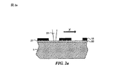
図2aは、電子遮断構造が設けられた電子小ビーム受け面を有するYAG1を概略的に示す横断面図である。電子遮断構造は、電子を遮断することができる遮断層18が設けられた電子遮断領域を有する。遮断層18は、金属層であることができる。電子を遮断するのに適した金属は、タングステンである。遮断領域の間には、非遮断領域がある。電子遮断構造の非遮断領域上に衝突する電子ビーム22は、実際には、YAG1の表面又はYAGの表面のコーティングに衝突する。
FIG. 2a is a cross-sectional view schematically showing YAG1 having an electron beam receiving surface provided with an electron blocking structure. The electron blocking structure has an electron blocking region provided with a
電子を遮断するためのいくつかの部分内には、遮断層18に加えて追加層21があることができる。追加層21は、金属層であることができ、遮断層18のエッジの鋭さを増加させる目的を果たすことができる。これは、遮断層のエッチングプロセスに耐性のある追加層の材料を選択することによって達成される。タングステンが遮断層の材料として選択されたとき、追加層21に適した材料は、クロムである。
In some parts for blocking electrons, there can be an
YAG1は、導電コーティング層20で覆われていることができる。このコーティングの目的は、入ってくる荷電粒子小ビームの結果として生じうるYAG1の帯電を防ぐことである。コーティングが、背景放射を遮断するために使用されることができる。コーティング層20に適した材料は、アルミニウム及びチタンを含む。
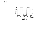
先に述べられたように、電子ビーム22の位置を測定するために、電子ビーム22は、(図2aにX方向として定義された方向に)YAG1に設けられた遮断構造の上を走査されることができる。これに応答して、YAG1内に発生された光がカメラで検出されることができる。このような走査及び検出動作の例示的な結果が、図2bに概略的に描かれる。
As mentioned earlier, to measure the position of the electron beam 22, the electron beam 22 is scanned over the blocking structure provided in YAG 1 (in the direction defined as the X direction in FIG. 2a). be able to. In response, the light generated in
図2bは、変換素子1の表面上の電子ビーム22のx位置の関数としての変換素子1によって放出された光の強度を示すグラフである。電子ビーム22が非遮断領域に完全に配置されたとき、最大の応答が観察され、電子ビーム22が遮断領域の上面に完全に配置されたとき、最小の光が発生される。ナイフエッジと交差すると、光強度の急激な変化をもたらす。
FIG. 2 b is a graph showing the intensity of the light emitted by the
所定の方向に電子ビームを走査する際、電子小ビームは、ナイフエッジと交差するとき2つのタイプの状況に遭遇しうる。第1の状況では、小ビームは、遮断領域から非遮断領域へ移行する。第2の状況では、小ビームは、非遮断領域から遮断領域へ移行する。 When scanning the electron beam in a given direction, the electron beamlet can encounter two types of situations when it intersects the knife edge. In the first situation, the beamlet moves from the blocking area to the non-blocking area. In the second situation, the beamlet moves from the non-blocking region to the blocking region.
第1の状況に対応する移行中に遭遇するナイフエッジは、第1のタイプのナイフエッジと称されることができる。同様に、第2の状況に対応する移行中に遭遇するナイフエッジは、第2のタイプのナイフエッジと称されることができる。ナイフエッジのタイプは、このように、測定される小ビームの走査方向によって決まる。「同様のタイプのナイフエッジ」が参照されたとき、これは、含まれる全てのナイフエッジが第1のタイプのナイフエッジに関連するか、第2のタイプのナイフエッジに関連するかであることを意味している。 The knife edge encountered during the transition corresponding to the first situation can be referred to as a first type of knife edge. Similarly, a knife edge encountered during a transition corresponding to a second situation can be referred to as a second type of knife edge. The type of knife edge is thus determined by the scanning direction of the small beam to be measured. When “similar types of knife edges” are referred to, this is whether all included knife edges are associated with a first type knife edge or a second type knife edge. Means.
変換素子の表面の電子受け面に設けられたナイフエッジのパターンの情報は、ビーム位置の測定を可能にする。小ビーム位置は、x方向に変換素子の表面を横切って小ビームを走査して、図2bに示されるように、変換素子によって放出された光の強度が最大値から最小値に、又は最小値から最大値に変化する位置を測定することによって測定されることができる。例えば、強度が最大値から最小値に変わるとき、これは、小ビームがx方向で非遮断領域から遮断領域へ移行するナイフエッジの上を走査されたことを示している。しかしながら、小ビームがどのナイフエッジに位置されているかに関して不確実性がありうる。 Information on the pattern of the knife edge provided on the electron receiving surface of the surface of the conversion element enables measurement of the beam position. The small beam position scans the small beam across the surface of the transducer element in the x direction, and the intensity of light emitted by the transducer element is either from a maximum value to a minimum value, or a minimum value, as shown in FIG. 2b. Can be measured by measuring the position that changes from to the maximum value. For example, when the intensity changes from a maximum value to a minimum value, this indicates that the beamlet has been scanned over a knife edge that transitions from the non-blocking region to the blocking region in the x direction. However, there can be uncertainty as to which knife edge the beamlet is located.
図2bに示される測定、及び小ビーム位置測定の説明は、一般的に、含まれる遮断領域及び非遮断領域の幅よりも小さい寸法を有する小ビームに関することに注意する。これらの寸法及び幅は、使用される走査方向に平行な方向に沿って取られる。 Note that the measurements shown in FIG. 2b and the description of the small beam position measurement generally relate to small beams having dimensions smaller than the width of the included blocking and non-blocking regions. These dimensions and widths are taken along a direction parallel to the scanning direction used.
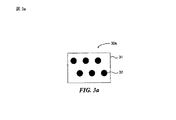
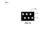
図3a並びに図3bは、本発明のいくつかの実施の形態で使用されることができる2つの異なる2次元遮断パターンを概略的に示す上面図である。両2次元遮断パターンは、複数のほぼ円形のフィーチャを含む。図3aでは、円形のフィーチャは、透過性の表面の上面にある遮断フィーチャであり、一方、図3bの2次元遮断パターンは、複数のほぼ円形のアパーチャが設けられた非遮断層によって形成されている。好ましくは、円形のフィーチャ間のピッチは、図6並びに図7を参照して説明されるのと同じようなマルチ小ビーム露光装置に設けられる小ビームのピッチに対応する。 Figures 3a and 3b are top views schematically illustrating two different two-dimensional blocking patterns that can be used in some embodiments of the present invention. Both two-dimensional blocking patterns include a plurality of substantially circular features. In FIG. 3a, the circular features are blocking features on the top surface of the permeable surface, while the two-dimensional blocking pattern of FIG. 3b is formed by a non-blocking layer provided with a plurality of substantially circular apertures. Yes. Preferably, the pitch between the circular features, corresponding to the pitch of the beamlets provided similar multi beamlet exposure apparatus as is described with reference to FIGS. 6 and 7.
図4は、複数の測定の配置を概略的に示す図であり、各測定の配置は、例えば図3a又は図3bに示されるような遮断パターンである2次元遮断パターンの選択された一部分でされる測定を表している。各測定で、フィーチャ43が荷電粒子小ビームで露光される。フィーチャを露光することは、小ビームで2次元走査を実行するとき、例えば、ビームのオン/オフを切り替えることによって、あるいは、小ビームを遮断するか通過させることによって、荷電粒子小ビームによって2次元パターンが形成されることを意味している。フィーチャが露光される位置は、各測定で異なる。さまざまな測定の配置におけるフィーチャの複数の位置が2次元グリッドを形成し、これは、図4では、グリッドセル41である2次元グリッドの形態を概略的に取る。各配置において、露光されるフィーチャ43は、さまざまなグリッドセル41の中心に置かれている。図4に示される例示的な2次元グリッドは、7×7=49のグリッドセル41を含む。
FIG. 4 schematically illustrates a plurality of measurement arrangements, where each measurement arrangement is a selected portion of a two-dimensional blocking pattern, for example a blocking pattern as shown in FIG. 3a or 3b. Represents a measurement. In each measurement, feature 43 is exposed with a charged particle beam. Exposing a feature can be performed two-dimensionally by a charged particle beam when performing a two-dimensional scan with a beam, for example by switching the beam on or off, or by blocking or passing the beam. It means that a pattern is formed. The location where the feature is exposed is different for each measurement. The multiple locations of the features in various measurement arrangements form a two-dimensional grid, which in FIG. 4 schematically takes the form of a two-dimensional grid, which is a
例えば、最も左上側の配置は、2次元(7×7)グリッドの1行1列によって形成されたグリッドセル41のその中心で露光されるフィーチャ43を描いている。同様に、最も右下側の配置は、2次元(7×7)グリッドの最終行最終列によって形成されたグリッドセル41のその中心で露光されるフィーチャ43を描いている。簡略化のために、49のすべての可能な配置は示されないが、露光されるフィーチャ位置が2次元(7×7)グリッドにおいて1行、4行又は7行及び1列、2列、5列又は7列によって形成されたグリッドセル41に対応している配置が示される。
For example, the upper leftmost arrangement depicts a feature 43 that is exposed at its center of a
2次元グリッドは、センサ表面領域に設けられた小ビーム遮断領域及び非遮断領域の2次元パターンの一部分の上に投影される。センサは、荷電粒子のエネルギを光に変換するための変換素子を有する。変換素子によって発生された光は、2次元パターン内の非遮断領域を透過された荷電粒子に応答して受光される。受光された光は、CCDカメラなどの光感応検出器を使用して光強度値に変換されることができる。 The two-dimensional grid is projected onto a portion of the two-dimensional pattern of small beam blocking areas and non-blocking areas provided in the sensor surface area. The sensor has a conversion element for converting the energy of charged particles into light. The light generated by the conversion element is received in response to charged particles that have been transmitted through the non-blocking region in the two-dimensional pattern. The received light can be converted to a light intensity value using a light sensitive detector such as a CCD camera.
各測定では、光強度値は、受光された光の変換によって得られる。そして、光強度値が、露光されたフィーチャがその上の中心に置かれたグリッドセル41に割り当てられる。この結果、7×7=49のこの例において光強度値が得られることができる。
In each measurement, the light intensity value is obtained by conversion of the received light. The light intensity value is then assigned to the
例えば、図4に示される配置を生成するためにさまざまな位置で測定をすることは、さまざまなやり方で達成されることができる。1つのアプローチは、測定の間に2次元パターンを移動させることである。例えば、図4では、図4の最も左上の測定の配置(1行1列)から始めて、2次元パターンが、左上の測定の配置に隣接した測定の配置に、すなわち2次元グリッドの1行2列によって形成されたグリッドセル41で中心に置かれた小ビーム投影での測定の配置に達するように、単一のグリッドセル41の幅に対応する距離だけ移動されることができる。
For example, taking measurements at various locations to generate the arrangement shown in FIG. 4 can be accomplished in various ways. One approach is to move the two-dimensional pattern during the measurement. For example, in FIG. 4, starting from the top left measurement layout (one row and one column) of FIG. 4, the two-dimensional pattern is a measurement layout adjacent to the top left measurement layout, ie, one
さまざまな位置で測定する他のやり方は、1以上の静電デフレクタの使用による。測定の間に小ビームを適切に偏向することによって、小ビームが次に測定される所望のグリッドセルの中心に置かれ、2次元画像が生成されることができる。 Another way to measure at various locations is through the use of one or more electrostatic deflectors. By appropriately deflecting the beam during the measurement, the beam can be centered on the desired grid cell to be measured next and a two-dimensional image can be generated.
測定をするさらなる他のやり方は、露光装置の描画スキームを使用する。代表的には、描画スキームは、所定の経路に沿った表面上の小ビームの移動を含む。小ビーム(のオン又はオフ)を変調することによって、パターンが表面上に描画される。小ビームの移動は、ターゲット面に対するビームの機械的な移動や1以上の静電デフレクタによる偏向移動を含むことができる。2次元パターン上を2次元経路に沿って小ビームを走査することによって、測定経路の一部分の間、小ビームが2次元パターンを露光することを可能にしながら、測定がされることができる。このような走査が繰り返し実行されると、2次元パターンが露光される走査経路の一部分が各測定で異なるが、図4に示されるような測定の配置のシーケンスが形成され、グリッド位置の関数としての強度値の2次元画像が生成されることができる。 Yet another way to make the measurement uses the exposure apparatus drawing scheme. Typically, the drawing scheme involves the movement of a small beam on the surface along a predetermined path. By modulating the small beam (on or off), a pattern is drawn on the surface. Small beam movement can include mechanical movement of the beam relative to the target surface and deflection movement by one or more electrostatic deflectors. By scanning the small beam along the two-dimensional path over the two-dimensional pattern, measurements can be made while allowing the small beam to expose the two-dimensional pattern during a portion of the measurement path. When such a scan is repeatedly performed, a part of the scan path where the two-dimensional pattern is exposed differs for each measurement, but a sequence of measurement arrangements as shown in FIG. 4 is formed as a function of grid position. A two-dimensional image of intensity values can be generated.
図5は、2次元グリッドがその上に投影されることができる2次元パターンの一例を概略的に示す図である。この特定の例では、2次元パターンは、アパーチャ52と称される非遮断円形領域52を含む遮断層51で形成される。このような2次元パターンを用いて、光感応検出器で受光された光強度は、アパーチャ52及び荷電粒子小ビーム43が互いにアライメントされた測定位置で最大強度値に達する。図5の2次元パターンが図4に描かれ図4を参照して説明されるような複数の測定に使用され、小ビームの位置が完全に予期された通りであるならば、最大強度値は、2次元グリッドの4行4列によって形成されたグリッドセル41に対応する位置で投影された小ビーム43で得られる。結局、このグリッドセルは、アパーチャ52の完全に上にある。しかしながら、小ビームがわずかに異なる位置にあれば、最大強度は、さまざまな位置にある投影された小ビーム43で得られることができる。
FIG. 5 is a diagram schematically illustrating an example of a two-dimensional pattern on which a two-dimensional grid can be projected. In this particular example, the two-dimensional pattern is formed with a
好ましくは、アパーチャ52は、センサ表面上の露光中、小ビーム43の予期される投影サイズと同じサイズである。このような同様のサイズは、測定の感度を増加させる。なぜならば、完全な相互アライメント位置からの小さなずれが、既に検出された光強度値の識別可能な減少を既にもたらしているからである。
Preferably, the
2次元パターンで得られる複数の測定は、2次元画像の生成を可能にし、グリッド位置の関数としての光強度を示している。フィッティングアルゴリズムが、サブグリッドセルの精度でアパーチャ52に対する小ビーム43の実際の位置を得るために、結果として生じる2次元画像に適用されることができる。このようなフィッティングアルゴリズムは、2次元画像上への2次元(2D)ガウス関数のフィッティングを含むことができる。本発明者らは、これらの相互アライメントの関数としてセンサ表面上のほぼ円形の小ビーム投影の円形アパーチャのたたみ込みは、2Dガウス関数に非常によく似ていることを理解している。
The multiple measurements obtained with a two-dimensional pattern allow the generation of a two-dimensional image and indicate the light intensity as a function of grid position. A fitting algorithm can be applied to the resulting two-dimensional image to obtain the actual position of the beam 43 relative to the
本発明の実施の形態は、単一のフィーチャ、すなわちアパーチャ52で単一の小ビーム43及び2次元パターンを参照して説明されてきた。しかしながら、本発明のいくつかの実施の形態もまた、複数の小ビームの小ビーム位置を測定するために使用されることができる。このような場合、2次元パターンは、アパーチャなどの複数のフィーチャを含むことができ、各小ビームがさまざまなフィーチャに対して測定される。
Embodiments of the present invention have been described with reference to a single feature, ie, a single beamlet 43 and two-dimensional pattern at the
図6は、複数の小ビーム61、62の配置を概略的に示す図である。図7は、荷電粒子遮断層72における複数のアパーチャ71の2次元パターン70を概略的に示す図である。点のある表面で概略的に示される小ビーム61の位置は、図7の2次元パターン70のアパーチャ71上に投影された2次元グリッドに関して図4を参照して説明されるような測定を行うことによって測定される。
FIG. 6 is a diagram schematically showing the arrangement of the plurality of
図6は、選択された小ビーム61のみが測定方法に従うことを示しているが、全ての小ビーム61、62を使用することが可能であり、従って、現在選択されていない小ビーム62を含む。しかしながら、測定方法において小ビーム61の選択を使用することは、各選択された小ビームの位置を測定するために必要とされる処理パワーがより少ないという利点を有する。さらに、特に、小ビーム間のピッチPが非常に小さい、例えば50nm未満であれば、十分に正確な2次元パターンを製造するのは比較的複雑でコストがかかる。「ピッチ」との表現は、所定の方向で、一般的にはマルチ小ビーム露光装置の機械走査方向にほぼ垂直な方向における2つの隣接する小ビームの間の公称距離を意味することが理解される。2次元パターンの製造上の必要条件を低減させることは、測定に加わる小ビーム61を1つおきに選択することによって達成されることができる。そして、他の小ビーム62の位置は、例えば、近隣の選択された小ビーム61の測定された位置に適用される内挿技術を使用することによって見積もられることができる。
FIG. 6 shows that only the selected
さらに、複数の小ビーム61の並列測定が、小ビーム61の一部であるサブビームの位置の測定をもたらすことができる。並列な複数の測定の使用は、サブビーム位置測定の信号対雑音比を増加させる。
Furthermore, parallel measurement of a plurality of
理論上、マルチ小ビーム露光システムにおける小ビームは、既知の設計に従って離間されている。結果として、設計内の個々の小ビーム間で、例えば仮想完全系のx座標及びy座標として定義される公称ベクトル距離が知られている。この情報は、スティッチングを制御するために使用されることができる。しかしながら、実際的な制限のため、小ビーム間の実際のベクトル距離は公称ベクトル距離と同一ではない。結果として、いわゆるスティッチングエラーが生じうる。スティッチングエラーは、公称位置と、表面をパターニングする小ビームの実際の位置との間のベクトルのずれとして定義されることができる。 Theoretically, the beamlets in a multi-beamlet exposure system are spaced according to a known design. As a result, nominal vector distances are known between individual beamlets in the design, for example defined as the x- and y-coordinates of the virtual complete system. This information can be used to control stitching. However, due to practical limitations, the actual vector distance between the beamlets is not the same as the nominal vector distance. As a result, so-called stitching errors can occur. Stitching error can be defined as the vector offset between the nominal position and the actual position of the beamlet patterning the surface.
上に説明される測定方法は、さらに、変換素子の荷電粒子受け面の表面の平面での第1の小ビームと第2の小ビームとの間の実際のベクトル距離を測定するために使用されることができる。さらに、2つの小ビーム間の公称ベクトル距離からのずれが得られることができる。2つの小ビーム間の実際のベクトル距離を測定すること、あるいは、付加的又は代替的に、2つの小ビーム間の公称ベクトル距離からずれを測定することは、それぞれの小ビームを使用してマルチ小ビーム露光装置でターゲット面を露光することから生じうるスティッチングエラーを予測するのに有用であることができる。実際のベクトル距離が知られていれば、制御データは、これら小ビームに対して測定された実際のベクトル距離による公称ベクトル距離の置換によって補正されることができる。公称ベクトル距離からのずれが知られていれば、適切な補正がそれぞれの小ビームの少なくとも1つの制御データを補正することによってなされることができる。 The measurement method described above is further used to measure the actual vector distance between the first and second beamlets in the plane of the surface of the charged particle receiving surface of the transducer element. Can. Furthermore, a deviation from the nominal vector distance between the two beamlets can be obtained. Measuring the actual vector distance between two beamlets, or in addition or alternatively, measuring the deviation from the nominal vector distance between two beamlets, can be achieved using multiple beamlets. It can be useful for predicting stitching errors that can result from exposing a target surface with a small beam exposure apparatus. If the actual vector distance is known, the control data can be corrected by replacing the nominal vector distance with the actual vector distance measured for these beamlets. If the deviation from the nominal vector distance is known, an appropriate correction can be made by correcting at least one control data for each beamlet.
第1の小ビームと第2の小ビームとの間の実際のベクトル距離を測定するための方法の実施の形態は、以下のことを含むことができる。まず、第1の小ビームの小ビーム位置が、荷電粒子マルチ小ビーム露光装置において小ビーム位置を測定するための上述の方法の実施の形態を使用して測定される。そして、2次元パターンが、所定のベクトル距離にわたってセンサ表面の平面にほぼ平行な方向に搬送される。所定のベクトル距離が、センサの荷電粒子受け面の表面の平面において所定の方向で所定の距離として定義される。所定の距離は、一般的に、第1の小ビームと第2の小ビームとの間の理論上の距離に対応する。同様に、所定の方向は、一般的に、第1の小ビームから始まり第2の小ビームが予期される方向に対応する。 An embodiment of a method for measuring an actual vector distance between a first beamlet and a second beamlet can include the following. First, the beam position of the first beam is measured using the above-described method embodiment for measuring beam position in a charged particle multi-beam exposure apparatus. The two-dimensional pattern is then conveyed in a direction substantially parallel to the plane of the sensor surface over a predetermined vector distance. A predetermined vector distance is defined as a predetermined distance in a predetermined direction in the plane of the surface of the charged particle receiving surface of the sensor. The predetermined distance generally corresponds to the theoretical distance between the first beamlet and the second beamlet. Similarly, the predetermined direction generally corresponds to the direction in which a second beamlet is expected, starting with the first beamlet.
代表的には、2次元パターンの搬送は、第1の小ビーム及び第2の小ビームによる2次元パターンの露光をするための最も容易な方法である。しかしながら、所定のベクトル距離にわたって第2の小ビームを移動させるか、互いに関連して小ビームと2次元パターンとの間の相対移動を与えることも実現可能でありうる。 Typically, transport of a two-dimensional pattern is the easiest method for exposing a two-dimensional pattern with a first small beam and a second small beam. However, it may also be feasible to move the second beamlet over a predetermined vector distance or to provide a relative movement between the beamlet and the two-dimensional pattern relative to each other.
そして、第2の小ビームの小ビーム位置は、荷電粒子マルチ小ビーム露光装置において小ビーム位置を測定するための上述の方法の実施の形態を使用して測定される。このように、複数の測定が、複数の測定位置が2次元グリッドを形成するさまざまな位置でなされ、各測定は、第2の小ビームで2次元パターンの一部分を露光することと、2次元パターンの非遮断領域を透過された第2の小ビームの一部分である荷電粒子に応答して変換素子によって発生された光を受光することと、光感応検出器によって受光した光をさらなる強度値に変換することとを含む。そして、第2の小ビームの位置が、2次元グリッド内のさまざまな位置でさらなる光強度値によって生成されたさらなる2次元画像に基づいて2次元パターンに対して測定される。 The beam position of the second beam is then measured using the above-described method embodiment for measuring beam position in a charged particle multi-beam exposure apparatus. Thus, multiple measurements are made at various positions where multiple measurement positions form a two-dimensional grid, each measurement exposing a portion of the two-dimensional pattern with a second beamlet and the two-dimensional pattern. Receiving light generated by the conversion element in response to charged particles that are part of the second small beam transmitted through the non-blocking region of the light and converting the light received by the photosensitive detector into further intensity values Including. The position of the second beamlet is then measured against the two-dimensional pattern based on additional two-dimensional images generated by additional light intensity values at various positions in the two-dimensional grid.
最後に、第1の小ビームと第2の小ビームとの間の実際の距離は、第1の小ビームの測定された小ビーム位置と、第2の小ビームの測定された小ビーム位置と、所定のベクトル距離とに基づいて測定される。 Finally, the actual distance between the first beamlet and the second beamlet is the measured beamlet position of the first beamlet and the measured beamlet position of the second beamlet. , Based on a predetermined vector distance.
再び、2つの小ビーム間の実際の距離の測定に加えて、このような測定は、複数の小ビーム内の複数の小ビーム対に対して並列に行われることができる。このような並列測定は、行われる測定の信号対雑音比を改良する。 Again, in addition to measuring the actual distance between two beamlets, such a measurement can be performed in parallel for a plurality of beamlets within a plurality of beamlets. Such parallel measurements improve the signal-to-noise ratio of the measurements made.
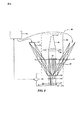
図8は、荷電粒子マルチ小ビームリソグラフィシステム80の一実施の形態を示す簡略化された概略図である。リソグラフィシステム80は、適切には、複数の小ビームを発生する小ビームジェネレータと、変調された小ビームを形成するために小ビームをパターニングする小ビームモジュレータと、変調された小ビームをターゲット表面上に投影するための小ビームプロジェクタとを有する。
FIG. 8 is a simplified schematic diagram illustrating one embodiment of a charged particle
小ビームジェネレータは、代表的には、発生源と、少なくとも1つのビームスプリッタとを有する。図8の発生源は、ほぼ均質に拡大する荷電粒子ビーム84を生成するために配置された荷電粒子源83である。以後、リソグラフィシステムの動作は、電子ビーム84を発生するために配置された電子源83に関連して説明される。
Small beam generators typically have a source and at least one beam splitter. The source of FIG. 8 is a charged
図8では、電子源83からの電子ビーム84は、電子ビーム84をコリメートするためのコリメータレンズ85を通過する。コリメータレンズ85は、任意のタイプのコリメート光学系であることができる。続いて、電子ビーム84は、図8の実施の形態ではアパーチャアレイ86であるビームスプリッタに衝突する。アパーチャアレイ86は、好ましくは、貫通孔を備えたプレートを有する。アパーチャアレイ86は、ビーム84のブロック部分に配置されている。さらに、アレイ86は、複数の平行な電子小ビーム87を生成するように通過することを可能にする。
In FIG. 8, the
図8のリソグラフィシステム80は、非常に多くの小ビーム87を、好ましくは10,000〜1,000,000の小ビームを発生させることができ、もちろんこれよりも多いか少ない小ビームが発生されることも可能である。第2のアパーチャアレイが、電子ビーム84からサブビームを生成し、サブビームから電子小ビーム87を生成するように、システムに追加されることができる。これは、さらに下流側でのサブビームの操作を可能にし、特にシステムにおける小ビームの数が5,000以上であるとき、システムオペレーションのために有益であることがわかっている。
The
小ビームモジュレータは、代表的には、複数のブランカの配置を備えた小ビームブランカアレイ89を有する。代表的には、小ビームブランカアレイ89は、小ビーム停止アレイ90と協働する。ブランカは、電子小ビーム87の1以上を偏向することが可能である。本発明の実施の形態では、ブランカは、特に、第1の電極と、第2の電極とアパーチャとが設けられた静電デフレクタである。そして、電極は、アパーチャを横切る電場を発生させるためのアパーチャの反対側に位置されている。一般的に、第2の電極は、グラウンド電極、すなわちグラウンド電位に接続された電極である。ブランカアレイ89の平面内で電子小ビームを合焦させるために、リソグラフィシステムは、さらに、コンデンサレンズアレイを有することができる。
The small beam modulator typically has a small beam
図8の実施の形態では、小ビーム停止アレイ90は、小ビームが通過することを可能にするためのアレイアパーチャを有する。小ビーム停止アレイ90は、その基本形態では、代表的には円形であるが他の形状が使用されてもよい貫通孔が設けられた基板を有する。小ビームブランカアレイ89と小ビーム停止アレイ90とは、小ビーム87を遮断するか通過させるために一緒に動作する。いくつかの実施の形態では、小ビーム停止アレイ90のアパーチャは、小ビームブランカアレイ89の静電デフレクタのアパーチャとアライメントされている。小ビームブランカアレイ89が小ビームを偏向すると、小ビームは小ビーム停止アレイ90の対応するアパーチャを通過しない。代わって、小ビームは、小ビーム遮断アレイ90の基板によって遮断される。小ビームブランカアレイ89が小ビームを偏向しないと、小ビームは、小ビーム停止アレイ90の対応するアパーチャを通過する。いくつかの他の実施の形態では、小ビームブランカアレイ89と小ビーム停止アレイ90との共働は、ブランカアレイ89のデフレクタによる小ビームの偏向が小ビーム停止アレイ90の対応するアパーチャを通る小ビームの通過をもたらすようになっており、一方、非偏向は、小ビーム停止アレイ90の基板による遮断をもたらす。
In the embodiment of FIG. 8, the small
小ビームモジュレータは、制御ユニット100によって与えられる入力に基づいて小ビーム87にパターンを追加するために配置されている。制御ユニット100は、例えばクリーンルームの内部の外部で、システムの残りの部分から離れて位置されることができる。制御システム100は、さらに、アクチュエータシステム96に接続されることができる。アクチュエータシステムは、電子光学カラム、すなわち破線98によって図8に描かれる小ビームを発生し投影するためのリソグラフィシステム80の構成要素の相対移動及びターゲット位置決めシステム104を実行するために配置されている。
The small beam modulator is arranged to add a pattern to the small beam 87 based on the input provided by the
パターンデータを保持している変調された光ビーム94は、光ファイバを使用して小ビームブランカアレイ89に伝送される。特に、光ファイバアレイ95の光ファイバ端部部分からの変調された光ビーム94は、例えば1以上のレンズ97を使用することによって、小ビームブランカアレイ89に位置された対応する光感応要素に投影される。光感応要素は、光信号を異なるタイプの信号に、例えば電気信号に変換するために配置されることができる。変調された光ビーム94は、対応する光感応要素に結合された1以上のブランカを制御するためのパターンデータの一部分を保持する。いくつかの実施の形態では、光ビーム94は、少なくとも部分的に、導光路によって光感応要素に向かって伝送されることができる。
The modulated light beam 94 holding the pattern data is transmitted to the small beam
小ビームモジュレータから出てくる変調された小ビームは、小ビームプロジェクタによってターゲット93のターゲット面上にスポットとして投影される。小ビームプロジェクタは、代表的には、ターゲット面上で変調された小ビームを走査するための走査デフレクタと、ターゲット面上に変調された小ビームを合焦させるための投影レンズ系とを有する。これらは、シングルエンドモジュール内にあることができる。
The modulated small beam coming out of the small beam modulator is projected as a spot on the target surface of the
このようなエンドモジュールは、好ましくは、挿入可能で交換可能なユニットとして構成されている。エンドモジュールは、デフレクタアレイ91と、投影レンズ構成体92とを有することができる。挿入可能で交換可能なユニットはまた、上に説明されるような小ビーム停止アレイ90を含むことができる。エンドモジュールを出た後、小ビーム87は、ターゲットの平面に配置されたターゲット面に衝突する。リソグラフィ用途に関して、ターゲット93は、通常、荷電粒子感応層、すなわちレジスト層が設けられたウェーハである。
Such end modules are preferably configured as insertable and replaceable units. The end module can have a deflector array 91 and a projection lens arrangement 92. The insertable and replaceable unit can also include a
デフレクタアレイ91は、小ビーム停止アレイ90を通過した各小ビーム87を偏向するために配置された走査デフレクタアレイの形態を取ることができる。デフレクタアレイ91は、比較的小さな駆動の電圧の印加を可能にする複数の静電デフレクタを含むことができる。デフレクタアレイ91は、投影レンズ構成体92の上流側に描かれているが、デフレクタアレイ91も投影レンズ構成体92とターゲット面との間に配置されることができる。
The deflector array 91 can take the form of a scanning deflector array that is arranged to deflect each small beam 87 that has passed through the small
投影レンズ構成体92は、デフレクタアレイ91による偏向の前に、又は後に、小ビーム87を合焦させるために配置されている。好ましくは、合焦は、直径約10〜30ナノメートルの幾何学的なスポットサイズをもたらす。このような好ましい実施の形態では、投影レンズ構成体92は、好ましくは、約100〜500倍の縮小率を、好ましくはできるだけ大きな、例えば300〜500倍の範囲にある縮小率を与えるように配置されている。この好ましい実施の形態では、投影レンズ構成体92は、効果的には、ターゲット面に接近して位置されることができる。 The projection lens arrangement 92 is arranged to focus the small beam 87 before or after deflection by the deflector array 91. Preferably, focusing results in a geometric spot size with a diameter of about 10-30 nanometers. In such preferred embodiments, the projection lens arrangement 92 is preferably arranged to provide a reduction factor of about 100 to 500 times, preferably as large as possible, for example in the range of 300 to 500 times. Has been. In this preferred embodiment, the projection lens arrangement 92 can effectively be positioned close to the target surface.
一般に、ターゲット面は、基板上にレジスト膜を有する。レジスト膜のいくつかの部分は、荷電粒子の小ビーム、すなわち電子の適用によって化学的に変質される。その結果、フィルムの照射部分は、現像液で多かれ少なかれ溶解可能になり、ウェーハ上にレジストパターンをもたらす。ウェーハ上のレジストパターンは、続いて、半導体製造の分野で知られているような、インプリメンテーション、エッチング、蒸着工程によって、下層に転写されることができる。 Generally, the target surface has a resist film on a substrate. Some parts of the resist film are chemically altered by the application of a small beam of charged particles, ie electrons. As a result, the irradiated portion of the film becomes more or less soluble with the developer, resulting in a resist pattern on the wafer. The resist pattern on the wafer can then be transferred to the underlayer by implementation, etching, and deposition processes as is known in the semiconductor manufacturing art.
図8に示されるシステムでは、小ビーム位置を測定するためにさまざまな位置で測定をすることは、1以上のさまざまな技術を使用することによって達成されてもよい。 In the system shown in FIG. 8, taking measurements at various positions to measure the beam position may be accomplished by using one or more different techniques.
第1の可能性は、測定の間に2次元パターンを移動させることである。図8では、2次元パターンは、ターゲット位置決めシステム104に設けられることができる。制御システム100の制御下でアクチュエータシステム96を使用してターゲット位置決めシステム104を移動させることによって、2次元パターンが正確であるようにして移動されることができる。
The first possibility is to move the two-dimensional pattern during the measurement. In FIG. 8, a two-dimensional pattern can be provided in the
2次元パターンの上述の移動と組み合わせられることができる第2のオプションは、1以上の静電デフレクタの使用である。そして、さまざまな位置で測定をすることは、小ビームを適切に偏向することによって達成されてもよい。このような静電デフレクタは、他の目的のための荷電粒子マルチ小ビーム露光装置に既にあってもよく、例えば、1以上のデフレクタが図8のシステム80におけるデフレクタアレイ91の一部であることができる。あるいは、1以上の静電デフレクタは、露光装置において小ビーム位置を測定する目的のために設けられる。
A second option that can be combined with the above-described movement of the two-dimensional pattern is the use of one or more electrostatic deflectors. And measuring at various positions may be accomplished by appropriately deflecting the beamlets. Such an electrostatic deflector may already be in a charged particle multi-beamlet exposure apparatus for other purposes, for example one or more deflectors being part of the deflector array 91 in the
小ビーム位置を測定するためにさまざまな位置で測定をする他のやり方は、走査経路の一部分の間、小ビームが2次元パターンを露光することを可能にしながら、2次元パターン上を2次元経路に沿って小ビームを走査することである。2次元グリッドにおけるさまざまな部分を形成するために、各測定で2次元パターンが露光される走査経路の部分は異なる。 Another way to measure at various positions to measure the beamlet position is to allow the beamlet to expose the two-dimensional pattern during a portion of the scan path, while the two-dimensional path over the two-dimensional pattern. Scanning a small beam along the line. In order to form various portions in the two-dimensional grid, the portion of the scan path where the two-dimensional pattern is exposed in each measurement is different.
本発明は、上に説明された所定の実施の形態を参照して説明されてきた。これら実施の形態が、本発明の意図及び範囲を逸脱することなく、当業者に周知のさまざまな変更及び変形を受けることができることが理解される。従って、特定の実施の形態が説明されてきたが、これらは単なる例であり、本発明の範囲を限定するものではなく、本発明の範囲は特許請求の範囲に規定される。
出願当初の特許請求の範囲に記載された発明を以下に付記する。
[1]荷電粒子マルチ小ビーム露光装置において小ビーム位置を測定するための方法であって、前記荷電粒子マルチ小ビーム露光装置には、荷電粒子のエネルギを光に変換するための変換素子と、光感応検出器とを有するセンサが設けられ、前記変換素子には、小ビーム遮断領域と非遮断領域との2次元パターンが設けられたセンサ表面領域が設けられ、この方法は、複数の測定をすることを具備し、各測定は、荷電粒子小ビームで前記2次元パターンの一部分上にフィーチャを露光することを含み、前記フィーチャが露光される位置は、各測定で異なり、複数の位置が2次元グリッドを形成し、2次元パターンの前記非遮断領域を透過された前記露光されたフィーチャの一部である荷電粒子に応答して前記変換素子によって発生された光を受光することと、前記光感応検出器によって受光された光を光強度値に変換して、測定がされた位置に前記光強度値を割り当てることとを含み、この方法は、前記2次元グリッド内のさまざまな位置で前記光強度値によって生成された2次元画像に基づいて前記2次元パターンに対する前記荷電粒子小ビームの位置を測定することを具備する方法。
[2]前記小ビーム遮断領域及び非遮断領域の前記2次元パターンは、非遮断孔が設けられた遮断面の形態を取る[1]の方法。
[3]前記孔は、ほぼ円形形状を有する[2]の方法。
[4]前記孔は、露光されるフィーチャのサイズと同じサイズである[3]の方法。
[5]前記小ビーム遮断領域及び非遮断領域の前記2次元パターンは、遮断フィーチャが設けられた非遮断面の形態を取る遮断する[1]の方法。
[6]前記遮断フィーチャは、ほぼ円形形状を有する[5]の方法。
[7]前記遮断フィーチャは、露光されるフィーチャのサイズと同じサイズである[6]の方法。
[8]前記露光されるフィーチャは、ほぼ円形形状を有する[1]ないし[7]のいずれか1の方法。
[9]荷電粒子小ビームで前記2次元パターンの一部分上にフィーチャを露光することは、荷電粒子小ビームが走査経路中の所定の一部分の間アクティブである間、前記2次元パターンの前記一部分上を2次元経路に沿って前記小ビームを走査することを含み、前記フィーチャが露光される位置が各測定で異なることは、各測定で前記走査経路の前記所定の一部分を変えることを含む[1]ないし[8]のいずれか1の方法。
[10]前記走査は、静電偏向によって行われる[9]の方法。
[11]前記荷電粒子小ビームの位置を測定することは、2Dガウス関数をフィッティングすることを含む[1]ないし[10]のいずれか1の方法。
[12]プロセッサによって実行されたとき、[1]ないし[11]のいずれか1の荷電粒子マルチ小ビーム露光装置で小ビーム位置を測定するための方法を行うためのコンピュータ読取可能媒体。
[13]荷電粒子マルチ小ビーム露光装置において2つの小ビーム間の距離を測定するための方法であって、前記荷電粒子マルチ小ビーム露光装置には、荷電粒子のエネルギを光に変換するための変換素子と、光感応検出器とを有するセンサが設けられ、前記変換素子には、小ビーム遮断領域と非遮断領域との2次元パターンが設けられたセンサ表面領域が設けられ、この方法は、[1]ないし[11]のいずれか1によって小ビーム位置を測定するための方法を行うことと、所定の距離にわたって前記センサの表面の平面にほぼ平行な方向に前記2次元パターンを搬送することと、複数の測定をすることとを具備し、各測定は、さらなる荷電粒子小ビームで前記2次元パターンの一部分上にフィーチャを露光することを含み、前記さらなる荷電粒子小ビームは、前記2次元パターンがその上を搬送される前記所定の距離に等しい前記荷電粒子小ビームからの理論上の距離を有し、前記フィーチャが露光される位置は、各測定で異なり、複数の位置が2次元グリッドを形成し、2次元パターンの前記非遮断領域を透過された前記露光されたフィーチャの一部である荷電粒子に応答して前記変換素子によって発生した光を受光することと、前記光感応検出器によって受光された光をさらなる光強度値に変換して、測定がされた位置に前記さらなる光強度値を割り当てることとを含み、この方法は、前記2次元グリッド内のさまざまな位置で前記さらなる光強度値によって生成された2次元画像に基づいて前記2次元パターンに対する前記さらなる荷電粒子小ビームの位置を測定することと、前記測定された荷電粒子小ビーム位置と、前記測定されたさらなる荷電粒子小ビーム位置と、前記所定の距離とに基づいて、前記荷電粒子小ビームと前記さらなる小ビームとの間の実際の距離を測定することとを具備する方法。
[14]前記さらなる荷電粒子小ビームで前記2次元パターンの一部分上にフィーチャを露光することは、前記さらなる荷電粒子小ビームが前記走査経路中の所定の一部分の間アクティブである間、前記2次元パターンの前記一部分上を2次元経路に沿って前記小ビームを走査することを含み、前記フィーチャが露光される位置が各測定で異なることは、各測定で前記走査経路の前記所定の一部分を変えることを含む[13]の方法。
[15]前記走査は、静電偏向によって行われる[13]の方法。
[16]前記さらなる荷電粒子小ビームの位置を測定することは、2Dガウス関数をフィッティングすることを含む[13]又は[14]の方法。
[17]プロセッサによって実行されたとき、[13]ないし[16]のいずれか1の荷電粒子マルチ小ビーム露光装置で2つの小ビーム間の実際の距離を測定するための方法を行うためのコンピュータ読取可能媒体。
The present invention has been described with reference to certain embodiments described above. It will be understood that these embodiments may be subject to various modifications and variations well known to those skilled in the art without departing from the spirit and scope of the present invention. Accordingly, although specific embodiments have been described, these are merely examples and are not intended to limit the scope of the invention, which is defined by the claims.
The invention described in the claims at the beginning of the application is appended below.
[1] A method for measuring a small beam position in a charged particle multi-small beam exposure apparatus, wherein the charged particle multi-small beam exposure apparatus includes a conversion element for converting energy of charged particles into light; A sensor having a light sensitive detector is provided, and the conversion element is provided with a sensor surface region provided with a two-dimensional pattern of a small beam blocking region and a non-blocking region. Each measurement includes exposing a feature on a portion of the two-dimensional pattern with a charged particle beam, the position at which the feature is exposed is different for each measurement, and a plurality of positions are 2 Light generated by the conversion element in response to charged particles that are part of the exposed features that form a dimensional grid and are transmitted through the unblocked region of a two-dimensional pattern. And converting the light received by the light sensitive detector into a light intensity value and assigning the light intensity value to the measured position, the method comprising: Measuring the position of the charged particle beamlet with respect to the two-dimensional pattern based on a two-dimensional image generated by the light intensity values at various positions.
[2] The method according to [1], wherein the two-dimensional pattern of the small beam blocking region and the non-blocking region takes the form of a blocking surface provided with a non-blocking hole.
[3] The method according to [2], wherein the hole has a substantially circular shape.
[4] The method of [3], wherein the hole is the same size as the size of the feature to be exposed.
[5] The method of [1], wherein the two-dimensional pattern of the small beam blocking area and the non-blocking area is blocked in the form of a non-blocking surface provided with blocking features.
[6] The method of [5], wherein the blocking feature has a substantially circular shape.
[7] The method of [6], wherein the blocking feature is the same size as the size of the feature to be exposed.
[8] The method according to any one of [1] to [7], wherein the exposed feature has a substantially circular shape.
[9] Exposing a feature on a portion of the two-dimensional pattern with a charged particle beam is on the portion of the two-dimensional pattern while the charged particle beam is active for a predetermined portion in the scan path. Scanning the beamlet along a two-dimensional path, wherein the position at which the feature is exposed is different for each measurement includes changing the predetermined portion of the scanning path for each measurement [1. ] To any one of [8].
[10] The method according to [9], wherein the scanning is performed by electrostatic deflection.
[11] The method according to any one of [1] to [10], wherein measuring the position of the charged particle beam includes fitting a 2D Gaussian function.
[12] A computer-readable medium for performing a method for measuring a beam position with the charged particle multi beam exposure apparatus according to any one of [1] to [11] when executed by a processor.
[13] A method for measuring a distance between two small beams in a charged particle multi-small beam exposure apparatus, wherein the charged particle multi-small beam exposure apparatus is for converting energy of charged particles into light. A sensor having a conversion element and a light-sensitive detector is provided, and the conversion element is provided with a sensor surface region provided with a two-dimensional pattern of a small beam blocking region and a non-blocking region. Performing a method for measuring the beam position according to any one of [1] to [11], and conveying the two-dimensional pattern in a direction substantially parallel to a plane of the sensor surface over a predetermined distance. And measuring a plurality of measurements, each measurement comprising exposing a feature on a portion of the two-dimensional pattern with a further charged particle beam. The particle beam has a theoretical distance from the charged particle beam that is equal to the predetermined distance over which the two-dimensional pattern is conveyed, and the position at which the feature is exposed is determined at each measurement. Unlike, a plurality of positions form a two-dimensional grid and receive light generated by the conversion element in response to charged particles that are part of the exposed features transmitted through the unblocked region of a two-dimensional pattern. And converting the light received by the light sensitive detector into a further light intensity value and assigning the further light intensity value to the measured position, the method comprising: Measuring the position of the further charged particle beamlets with respect to the two-dimensional pattern based on a two-dimensional image generated by the further light intensity values at various positions within. Based on the measured charged particle beamlet position, the measured further charged particle beamlet position, and the predetermined distance, the actual between the charged particle beamlet and the further beamlet Measuring the distance.
[14] exposing a feature on a portion of the two-dimensional pattern with the additional charged particle beam, while the additional charged particle beam is active during a predetermined portion of the scan path. Scanning the beamlet along the two-dimensional path over the portion of the pattern, wherein the position at which the feature is exposed is different for each measurement, changing the predetermined portion of the scan path with each measurement The method of [13] including this.
[15] The method according to [13], wherein the scanning is performed by electrostatic deflection.
[16] The method of [13] or [14], wherein measuring the position of the further charged particle beam comprises fitting a 2D Gaussian function.
[17] A computer for performing a method for measuring an actual distance between two small beams with the charged particle multi-small beam exposure apparatus according to any one of [13] to [16] when executed by a processor A readable medium.
Claims (17)
前記荷電粒子小ビームを使用して複数の測定をすることを具備し、各測定は、
前記荷電粒子小ビームで前記2次元パターンの一部分上に、ある位置で2次元フィーチャを露光することを含み、前記フィーチャが露光される位置は、各測定で異なり、複数の位置が2次元グリッドを形成し、
前記2次元パターンの前記非遮断領域を透過された前記露光されたフィーチャの一部である荷電粒子に応答して前記変換素子によって発生された光を受光することと、
前記光感応検出器によって、受光された光を光強度値に変換して、測定がされた位置に前記光強度値を割り当てることとを含み、
この方法は、
前記2次元グリッド内のさまざまな位置で前記光強度値によって生成された2次元画像に基づいて前記2次元パターンに対する前記荷電粒子小ビームの位置を測定することを具備する方法。 A method for measuring a beam position of a charged particle beam in a charged particle multi beam exposure apparatus, wherein the charged particle multi beam exposure apparatus includes a conversion element for converting the energy of charged particles into light. And a sensor having a photosensitive detector, and the conversion element is provided with a sensor surface region provided with a two-dimensional pattern of a small beam blocking region and a non-blocking region.
Making a plurality of measurements using the charged particle beam, each measurement comprising:
Exposing a two-dimensional feature at a position on a portion of the two-dimensional pattern with the charged particle beam, wherein the position at which the feature is exposed is different for each measurement, and a plurality of positions on a two-dimensional grid. Forming,
Receiving light generated by the conversion element in response to charged particles that are part of the exposed feature transmitted through the unblocked region of the two-dimensional pattern;
Converting light received by the light sensitive detector into a light intensity value and assigning the light intensity value to a measured position;
This method
Measuring the position of the charged particle beamlets relative to the two-dimensional pattern based on two-dimensional images generated by the light intensity values at various positions in the two-dimensional grid.
請求項1ないし11のいずれか1によって小ビーム位置を測定するための方法を行うことと、
所定の距離にわたって前記センサの表面の平面にほぼ平行な方向に前記2次元パターンを搬送することと、
さらなる荷電粒子小ビームを使用して複数の測定をすることとを具備し、各測定は、
前記さらなる荷電粒子小ビームで前記2次元パターンの一部分上に2次元フィーチャを露光することを含み、前記さらなる荷電粒子小ビームは、前記2次元パターンがその上を搬送される前記所定の距離に等しい前記荷電粒子小ビームからの理論上の距離を有し、前記フィーチャが露光される位置は、各測定で異なり、複数の位置が2次元グリッドを形成し、
2次元パターンの前記非遮断領域を透過された前記露光されたフィーチャの一部である荷電粒子に応答して前記変換素子によって発生した光を受光することと、
前記光感応検出器によって受光された光をさらなる光強度値に変換して、測定がされた位置に前記さらなる光強度値を割り当てることとを含み、
この方法は、
前記2次元グリッド内のさまざまな位置で前記さらなる光強度値によって生成された2次元画像に基づいて前記2次元パターンに対する前記さらなる荷電粒子小ビームの位置を測定することと、
前記測定された荷電粒子小ビーム位置と、前記測定されたさらなる荷電粒子小ビーム位置と、前記所定の距離とに基づいて、前記荷電粒子小ビームと前記さらなる小ビームとの間の実際の距離を測定することとを具備する方法。 A method for measuring a distance between two charged particle beamlets in a charged particle multibeam exposure device, the charged particle multibeam exposure device comprising a conversion for converting charged particle energy into light. A sensor having an element and a photosensitive detector is provided, and the conversion element is provided with a sensor surface region provided with a two-dimensional pattern of a small beam blocking region and a non-blocking region,
Performing a method for measuring a beam position according to any one of claims 1 to 11;
Conveying the two-dimensional pattern in a direction substantially parallel to a plane of the surface of the sensor over a predetermined distance;
Making a plurality of measurements using additional charged particle beamlets, each measurement comprising:
Exposing a two-dimensional feature onto a portion of the two-dimensional pattern with the additional charged particle beam, the additional charged particle beam being equal to the predetermined distance over which the two-dimensional pattern is conveyed The theoretical distance from the charged particle beam, the position at which the feature is exposed is different for each measurement, and a plurality of positions form a two-dimensional grid;
Receiving light generated by the conversion element in response to charged particles that are part of the exposed feature transmitted through the unblocked region of a two-dimensional pattern;
Converting the light received by the light sensitive detector into a further light intensity value and assigning the further light intensity value to the measured position;
This method
Measuring the position of the further charged particle beamlets relative to the two-dimensional pattern based on a two-dimensional image generated by the further light intensity values at various positions in the two-dimensional grid;
Based on the measured charged particle beamlet position, the measured further charged particle beamlet position, and the predetermined distance, an actual distance between the charged particle beamlet and the further beamlet is determined. Measuring.
Applications Claiming Priority (3)
| Application Number | Priority Date | Filing Date | Title |
|---|---|---|---|
| US201261646430P | 2012-05-14 | 2012-05-14 | |
| US61/646,430 | 2012-05-14 | ||
| PCT/EP2013/059861 WO2013171177A1 (en) | 2012-05-14 | 2013-05-14 | Method for determining a beamlet position and method for determining a distance between two beamlets in a multi-beamlet exposure apparatus |
Publications (3)
| Publication Number | Publication Date |
|---|---|
| JP2015517734A JP2015517734A (en) | 2015-06-22 |
| JP2015517734A5 JP2015517734A5 (en) | 2016-06-23 |
| JP6239595B2 true JP6239595B2 (en) | 2017-11-29 |
Family
ID=48463964
Family Applications (1)
| Application Number | Title | Priority Date | Filing Date |
|---|---|---|---|
| JP2015512021A Active JP6239595B2 (en) | 2012-05-14 | 2013-05-14 | Method for measuring beam position in a multi beam exposure apparatus and method for measuring the distance between two beam beams |
Country Status (6)
| Country | Link |
|---|---|
| US (2) | USRE49483E1 (en) |
| JP (1) | JP6239595B2 (en) |
| KR (1) | KR101959945B1 (en) |
| NL (1) | NL2010795C2 (en) |
| TW (1) | TWI582542B (en) |
| WO (1) | WO2013171177A1 (en) |
Families Citing this family (12)
| Publication number | Priority date | Publication date | Assignee | Title |
|---|---|---|---|---|
| DK2718211T3 (en) * | 2011-06-07 | 2015-12-07 | Carefusion Germany 326 Gmbh | DEVICE FOR ISOLATING UNIQUE GOODS TO BE STORED IN AN AUTOMATED STOCK |
| NL2012029C2 (en) * | 2013-12-24 | 2015-06-26 | Mapper Lithography Ip Bv | Charged particle lithography system with sensor assembly. |
| WO2016028335A1 (en) * | 2014-08-19 | 2016-02-25 | Intel Corporation | Corner rounding correction for electron beam (ebeam) direct write system |
| KR102330221B1 (en) | 2014-11-05 | 2021-11-25 | 삼성디스플레이 주식회사 | Organic light emitting device and display having the same |
| US10008364B2 (en) * | 2015-02-27 | 2018-06-26 | Kla-Tencor Corporation | Alignment of multi-beam patterning tool |
| KR102333285B1 (en) | 2015-08-20 | 2021-11-30 | 삼성전자주식회사 | Exposure apparatus |
| JP2018010895A (en) * | 2016-07-11 | 2018-01-18 | 株式会社ニューフレアテクノロジー | Blanking aperture array, manufacturing method of blanking aperture array, and multi charged-particle beam lithography apparatus |
| US11131541B2 (en) * | 2018-06-29 | 2021-09-28 | Taiwan Semiconductor Manufacturing Co., Ltd. | Shutter monitoring system |
| DE102018124044B3 (en) * | 2018-09-28 | 2020-02-06 | Carl Zeiss Microscopy Gmbh | Method for operating a multi-beam particle beam microscope and multi-beam particle beam system |
| WO2023110331A1 (en) * | 2021-12-17 | 2023-06-22 | Asml Netherlands B.V. | Charged-particle optical apparatus and projection method |
| EP4199031A1 (en) * | 2021-12-17 | 2023-06-21 | ASML Netherlands B.V. | Charged-particle optical apparatus and projection method |
| EP4202970A1 (en) * | 2021-12-24 | 2023-06-28 | ASML Netherlands B.V. | Alignment determination method and computer program |
Family Cites Families (14)
| Publication number | Priority date | Publication date | Assignee | Title |
|---|---|---|---|---|
| JPS5468149A (en) | 1977-11-11 | 1979-06-01 | Erionikusu Kk | Electron ray application device |
| JPS5570024A (en) | 1978-11-21 | 1980-05-27 | Chiyou Lsi Gijutsu Kenkyu Kumiai | Electron beam exposure method |
| JP2644257B2 (en) | 1988-03-08 | 1997-08-25 | 株式会社東芝 | Beam detection target |
| US6353231B1 (en) | 1998-08-31 | 2002-03-05 | Nikon Corporation | Pinhole detector for electron intensity distribution |
| EP1335249A1 (en) * | 2002-02-06 | 2003-08-13 | ASML Netherlands B.V. | Lithographic apparatus and device manufacturing method |
| JP3544657B2 (en) | 2002-09-13 | 2004-07-21 | 株式会社日立製作所 | Electron beam lithography system |
| US6958804B2 (en) | 2002-10-25 | 2005-10-25 | Mapper Lithography Ip B.V. | Lithography system |
| JP2005032508A (en) | 2003-07-10 | 2005-02-03 | Tokyo Seimitsu Co Ltd | Electron beam intensity distribution measuring device, electron beam device, electron beam exposure device, and electron beam intensity distribution measuring method |
| JP3962778B2 (en) | 2004-06-02 | 2007-08-22 | 株式会社日立ハイテクノロジーズ | Electron beam detector, electron beam writing method and electron beam writing apparatus using the same |
| JP4907092B2 (en) * | 2005-03-01 | 2012-03-28 | 株式会社日立ハイテクノロジーズ | Electron beam drawing apparatus and electron beam drawing method |
| US7868300B2 (en) | 2005-09-15 | 2011-01-11 | Mapper Lithography Ip B.V. | Lithography system, sensor and measuring method |
| EP1943662B1 (en) | 2005-09-15 | 2016-11-23 | Mapper Lithography IP B.V. | Lithography system, sensor and measuring method |
| NL1037820C2 (en) * | 2010-03-22 | 2011-09-23 | Mapper Lithography Ip Bv | Lithography system, sensor, sensor surface element and method of manufacture. |
| US9030675B2 (en) * | 2010-11-13 | 2015-05-12 | Mapper Lithography Ip B.V. | Method for determining a distance between two beamlets in a multi-beamlet exposure apparatus |
-
2013
- 2013-05-14 JP JP2015512021A patent/JP6239595B2/en active Active
- 2013-05-14 NL NL2010795A patent/NL2010795C2/en active
- 2013-05-14 KR KR1020147035204A patent/KR101959945B1/en active IP Right Grant
- 2013-05-14 TW TW102117002A patent/TWI582542B/en active
- 2013-05-14 US US16/414,386 patent/USRE49483E1/en active Active
- 2013-05-14 US US14/400,815 patent/US9653259B2/en not_active Ceased
- 2013-05-14 WO PCT/EP2013/059861 patent/WO2013171177A1/en active Application Filing
Also Published As
| Publication number | Publication date |
|---|---|
| WO2013171177A1 (en) | 2013-11-21 |
| TWI582542B (en) | 2017-05-11 |
| TW201400992A (en) | 2014-01-01 |
| WO2013171177A9 (en) | 2014-01-30 |
| KR20150013802A (en) | 2015-02-05 |
| KR101959945B1 (en) | 2019-03-19 |
| US20150155136A1 (en) | 2015-06-04 |
| JP2015517734A (en) | 2015-06-22 |
| NL2010795A (en) | 2013-11-18 |
| NL2010795C2 (en) | 2013-12-31 |
| USRE49483E1 (en) | 2023-04-04 |
| US9653259B2 (en) | 2017-05-16 |
Similar Documents
| Publication | Publication Date | Title |
|---|---|---|
| JP6239595B2 (en) | Method for measuring beam position in a multi beam exposure apparatus and method for measuring the distance between two beam beams | |
| JP5505821B2 (en) | Pattern lock device for particle beam exposure apparatus | |
| JP5688638B2 (en) | Pattern definition apparatus having a plurality of multi-beam arrays | |
| JP4995261B2 (en) | Particle beam exposure system with total modulation of patterned beam | |
| JP6931317B2 (en) | Charged particle lithography system with alignment sensor and beam measurement sensor | |
| US9373424B2 (en) | Electron beam writing apparatus and electron beam writing method | |
| JP6128744B2 (en) | Drawing apparatus, drawing method, and article manufacturing method | |
| JPH10214779A (en) | Electron beam exposure method and fabrication of device using that method | |
| JP7194572B2 (en) | Multi electron beam inspection system | |
| TW201303524A (en) | Method for splitting a pattern for use in a multi-beamlet lithography apparatus | |
| JP2017107959A (en) | Multi-charged particle beam device and method for adjusting the shape of multi-charged particle beam image | |
| JP7180515B2 (en) | Multi-charged particle beam writing apparatus and multi-charged particle beam writing method | |
| JP4612838B2 (en) | Charged particle beam exposure apparatus and exposure method therefor | |
| KR20140130029A (en) | Drawing apparatus, and method of manufacturing article | |
| US20130344443A1 (en) | Lithography apparatus, and method of manufacture of product | |
| JP2006080303A (en) | Electron beam drawing apparatus | |
| JP2006019434A (en) | Charged particle beam exposure method, charged particle beam exposure apparatus, and device manufacturing method | |
| US9040942B1 (en) | Electron beam lithography with linear column array and rotary stage | |
| US20020036272A1 (en) | Charged-particle-beam microlithography methods and apparatus providing reduced reticle heating | |
| JP2009146884A (en) | Electron gun, and electron beam device | |
| JPH09330869A (en) | Position detector and electron beam aligner with it |
Legal Events
| Date | Code | Title | Description |
|---|---|---|---|
| A521 | Request for written amendment filed |
Free format text: JAPANESE INTERMEDIATE CODE: A523 Effective date: 20160426 |
|
| A621 | Written request for application examination |
Free format text: JAPANESE INTERMEDIATE CODE: A621 Effective date: 20160426 |
|
| A977 | Report on retrieval |
Free format text: JAPANESE INTERMEDIATE CODE: A971007 Effective date: 20170131 |
|
| A131 | Notification of reasons for refusal |
Free format text: JAPANESE INTERMEDIATE CODE: A131 Effective date: 20170307 |
|
| A521 | Request for written amendment filed |
Free format text: JAPANESE INTERMEDIATE CODE: A523 Effective date: 20170406 |
|
| TRDD | Decision of grant or rejection written | ||
| A01 | Written decision to grant a patent or to grant a registration (utility model) |
Free format text: JAPANESE INTERMEDIATE CODE: A01 Effective date: 20171003 |
|
| A61 | First payment of annual fees (during grant procedure) |
Free format text: JAPANESE INTERMEDIATE CODE: A61 Effective date: 20171101 |
|
| R150 | Certificate of patent or registration of utility model |
Ref document number: 6239595 Country of ref document: JP Free format text: JAPANESE INTERMEDIATE CODE: R150 |
|
| S111 | Request for change of ownership or part of ownership |
Free format text: JAPANESE INTERMEDIATE CODE: R313113 |
|
| R350 | Written notification of registration of transfer |
Free format text: JAPANESE INTERMEDIATE CODE: R350 |
|
| RD02 | Notification of acceptance of power of attorney |
Free format text: JAPANESE INTERMEDIATE CODE: R3D02 |
|
| R250 | Receipt of annual fees |
Free format text: JAPANESE INTERMEDIATE CODE: R250 |
|
| R250 | Receipt of annual fees |
Free format text: JAPANESE INTERMEDIATE CODE: R250 |
|
| R250 | Receipt of annual fees |
Free format text: JAPANESE INTERMEDIATE CODE: R250 |
|
| R250 | Receipt of annual fees |
Free format text: JAPANESE INTERMEDIATE CODE: R250 |