JP4612838B2 - Charged particle beam exposure apparatus and exposure method therefor - Google Patents
Charged particle beam exposure apparatus and exposure method therefor Download PDFInfo
- Publication number
- JP4612838B2 JP4612838B2 JP2004378665A JP2004378665A JP4612838B2 JP 4612838 B2 JP4612838 B2 JP 4612838B2 JP 2004378665 A JP2004378665 A JP 2004378665A JP 2004378665 A JP2004378665 A JP 2004378665A JP 4612838 B2 JP4612838 B2 JP 4612838B2
- Authority
- JP
- Japan
- Prior art keywords
- charged particle
- particle beam
- array
- exposure
- intensity
- Prior art date
- Legal status (The legal status is an assumption and is not a legal conclusion. Google has not performed a legal analysis and makes no representation as to the accuracy of the status listed.)
- Expired - Fee Related
Links
Images


Classifications
-
- H—ELECTRICITY
- H01—ELECTRIC ELEMENTS
- H01J—ELECTRIC DISCHARGE TUBES OR DISCHARGE LAMPS
- H01J37/00—Discharge tubes with provision for introducing objects or material to be exposed to the discharge, e.g. for the purpose of examination or processing thereof
- H01J37/30—Electron-beam or ion-beam tubes for localised treatment of objects
- H01J37/317—Electron-beam or ion-beam tubes for localised treatment of objects for changing properties of the objects or for applying thin layers thereon, e.g. for ion implantation
- H01J37/3174—Particle-beam lithography, e.g. electron beam lithography
- H01J37/3177—Multi-beam, e.g. fly's eye, comb probe
-
- B—PERFORMING OPERATIONS; TRANSPORTING
- B82—NANOTECHNOLOGY
- B82Y—SPECIFIC USES OR APPLICATIONS OF NANOSTRUCTURES; MEASUREMENT OR ANALYSIS OF NANOSTRUCTURES; MANUFACTURE OR TREATMENT OF NANOSTRUCTURES
- B82Y10/00—Nanotechnology for information processing, storage or transmission, e.g. quantum computing or single electron logic
-
- B—PERFORMING OPERATIONS; TRANSPORTING
- B82—NANOTECHNOLOGY
- B82Y—SPECIFIC USES OR APPLICATIONS OF NANOSTRUCTURES; MEASUREMENT OR ANALYSIS OF NANOSTRUCTURES; MANUFACTURE OR TREATMENT OF NANOSTRUCTURES
- B82Y40/00—Manufacture or treatment of nanostructures
-
- H—ELECTRICITY
- H01—ELECTRIC ELEMENTS
- H01J—ELECTRIC DISCHARGE TUBES OR DISCHARGE LAMPS
- H01J37/00—Discharge tubes with provision for introducing objects or material to be exposed to the discharge, e.g. for the purpose of examination or processing thereof
- H01J37/02—Details
- H01J37/24—Circuit arrangements not adapted to a particular application of the tube and not otherwise provided for
- H01J37/243—Beam current control or regulation circuits
-
- H—ELECTRICITY
- H01—ELECTRIC ELEMENTS
- H01J—ELECTRIC DISCHARGE TUBES OR DISCHARGE LAMPS
- H01J37/00—Discharge tubes with provision for introducing objects or material to be exposed to the discharge, e.g. for the purpose of examination or processing thereof
- H01J37/30—Electron-beam or ion-beam tubes for localised treatment of objects
- H01J37/304—Controlling tubes by information coming from the objects or from the beam, e.g. correction signals
-
- H—ELECTRICITY
- H01—ELECTRIC ELEMENTS
- H01J—ELECTRIC DISCHARGE TUBES OR DISCHARGE LAMPS
- H01J2237/00—Discharge tubes exposing object to beam, e.g. for analysis treatment, etching, imaging
- H01J2237/04—Means for controlling the discharge
- H01J2237/045—Diaphragms
- H01J2237/0451—Diaphragms with fixed aperture
- H01J2237/0453—Diaphragms with fixed aperture multiple apertures
-
- H—ELECTRICITY
- H01—ELECTRIC ELEMENTS
- H01J—ELECTRIC DISCHARGE TUBES OR DISCHARGE LAMPS
- H01J2237/00—Discharge tubes exposing object to beam, e.g. for analysis treatment, etching, imaging
- H01J2237/30—Electron or ion beam tubes for processing objects
- H01J2237/304—Controlling tubes
- H01J2237/30472—Controlling the beam
Description
本発明は、荷電粒子線露光装置およびその露光方法に関する。 The present invention relates to a charged particle beam exposure apparatus and an exposure method thereof.
近年の半導体デバイスの高集積化、および超微細化に対応する手段のひとつとして、電子線等の荷電粒子ビームを用いた露光装置が開発されている。これまでは、上記露光装置は、スループットが低く、半導体デバイスの量産には適さないと考えられてきた。 An exposure apparatus using a charged particle beam such as an electron beam has been developed as one of means for dealing with high integration and ultraminiaturization of semiconductor devices in recent years. Until now, it has been considered that the exposure apparatus has a low throughput and is not suitable for mass production of semiconductor devices.
しかしながら、近年のステンシルマスク型の電子ビーム露光装置やマルチ電子ビーム露光装置の開発により量産に実用的なスループットが期待できるようになった。上記露光装置は、いずれも一度に露光する面積すなわち露光面積が従来に比べて広いため、スループットが改善できる。 However, due to the recent development of stencil mask type electron beam exposure apparatuses and multi electron beam exposure apparatuses, practical throughput can be expected for mass production. In any of the above-described exposure apparatuses, the area to be exposed at one time, that is, the exposure area, is wider than that of the conventional exposure apparatus.
ところが、ステンシルマスク型の荷電粒子線露光装置においては、ステンシルマスクを照射する荷電粒子線の照射域における強度が不均一であると、転写されるパターンが歪んでしまう。また、荷電粒子線露光装置においては、複数の荷電粒子ビームに強度のばらつきがあると、描画されるパターンが歪むという問題がある。特に、露光処理中に荷電粒子ビームの強度分布が変化して荷電粒子ビームに強度のばらつきが出てくると、露光装置の描画精度が著しく低下するという問題があった。
荷電粒子線露光装置で広範囲を均一にビーム照射するために、荷電粒子線源の改良、および光学系の改良が従来から行われている。しかしながら、これらの改良によって達成される照射均一性は不十分であった。 In order to uniformly irradiate a wide area with a charged particle beam exposure apparatus, improvement of a charged particle beam source and improvement of an optical system have been conventionally performed. However, the irradiation uniformity achieved by these improvements was insufficient.
また、荷電粒子線源から照射される荷電粒子線は、静的な強度不均一性だけでなく、荷電粒子線源自身および外部環境要因などによりその照射強度が変動する場合がある。照射強度の変動は、荷電粒子線露光装置において、照射域における荷電粒子ビームの予測不可能な強度分布不均一性となり、描画精度を劣化させる原因となる。 Further, the irradiation intensity of the charged particle beam irradiated from the charged particle beam source may fluctuate not only due to static intensity nonuniformity but also due to the charged particle beam source itself and external environmental factors. The fluctuation of the irradiation intensity causes an unpredictable intensity distribution non-uniformity of the charged particle beam in the irradiation region in the charged particle beam exposure apparatus, and causes a deterioration in drawing accuracy.
さらに、荷電粒子線源の交換や、構造体の保守などを行うことで、荷電粒子ビームの照射強度の均一性が失われる場合もある。 Furthermore, the uniformity of the irradiation intensity of the charged particle beam may be lost by exchanging the charged particle beam source or maintaining the structure.
したがって、静的に十分な照射強度の均一性が得られ、かつ実露光中の荷電粒子ビームに対し、リアルタイムに照射強度分布を検出し、補正する方法が求められてきた。 Therefore, there has been a demand for a method for detecting and correcting the irradiation intensity distribution in real time with respect to a charged particle beam during actual exposure, which can provide statically sufficient irradiation intensity uniformity.
これに対し、荷電粒子線露光装置において、各荷電粒子ビーム間の強度のばらつきを補正する方法として、アパーチャアレイに照射電流検出用のアパーチャを実装し、リアルタイムの照射強度分布検出を実施する方法(特開2004−193516号公報)や、ブランカーのオンオフ時間の制御によって露光時間を管理する方法(特開2003−051437号公報)が提案されていた。ところが、ブランカーのオンオフ時間の制御によって露光時間を管理する方法では、スループットを向上しようとすると、非常に高速なブランカーのオンオフ駆動制御が必要となり、厳密な時間管理が困難になるため、スループットの向上が制限されるという問題があった。 On the other hand, in a charged particle beam exposure apparatus, as a method of correcting variation in intensity between each charged particle beam, a method for implementing real-time irradiation intensity distribution detection by mounting an aperture for detecting an irradiation current on the aperture array ( Japanese Laid-Open Patent Publication No. 2004-193516) and a method of managing exposure time by controlling the on / off time of a blanker (Japanese Laid-Open Patent Publication No. 2003-051437) have been proposed. However, in the method of managing the exposure time by controlling the on / off time of the blanker, when trying to improve the throughput, it is necessary to control the on / off drive of the blanker at a very high speed, and it becomes difficult to strictly control the time. There was a problem that was limited.
本発明は、上記の点に鑑み、マルチビーム方式の荷電粒子線露光装置において、露光時に照射される荷電粒子ビームの強度分布を均一にすることができ、精度よくパターンを描画できる露光装置およびその露光方法を提供することを目的とする。 In view of the above points, the present invention provides a multi-beam type charged particle beam exposure apparatus that can uniformly distribute the intensity distribution of a charged particle beam irradiated during exposure and can accurately draw a pattern, and the exposure apparatus An object is to provide an exposure method.
上記目的を達成するために、本発明は、荷電粒子線源からの荷電粒子ビームをアパーチャアレイに設けられた複数の開口で複数の荷電粒子ビームに分割し、前記複数の荷電粒子ビームを用いて露光を行う荷電粒子線露光装置において、前記アパーチャアレイの開口を通過する前記荷電粒子ビームの強度を検出する検出手段と、前記検出手段の検出結果に基づいて前記荷電粒子ビームの強度を調整する調整手段と、を備え、前記調整手段は、グリッドアレイ上の複数の開口に形成された複数のグリッド電極を有し、前記グリッド電極に前記荷電粒子線源のアノードと同極の電圧を印加することで前記荷電粒子ビームの強度を調整することを特徴とする。 In order to achieve the above object, the present invention divides a charged particle beam from a charged particle beam source into a plurality of charged particle beams at a plurality of openings provided in an aperture array, and uses the plurality of charged particle beams. the charged particle beam exposure apparatus for performing exposure, and detecting means for detecting the intensity of the previous SL charged particle beam passing through the aperture of the aperture array, adjusting the intensity of the charged particle beam based on a detection result of said detecting means Adjusting means, and the adjusting means has a plurality of grid electrodes formed in a plurality of openings on the grid array, and applies a voltage having the same polarity as the anode of the charged particle beam source to the grid electrodes. In this way, the intensity of the charged particle beam is adjusted .
さらに、上記目的を達成するための本発明の露光方法は、荷電粒子線源からの荷電粒子ビームをアパーチャアレイに設けられた複数の開口で複数の荷電粒子ビームに分割し、前記複数の荷電粒子ビームを用いて露光を行う露光方法において、前記アパーチャアレイの開口を通過する前記荷電粒子ビームの強度を検出する検出工程と、前記検出工程での検出結果に基づいて前記荷電粒子ビームの強度を調整する調整工程と、を有し、前記調整工程では、グリッドアレイ上の複数の開口に形成された複数のグリッド電極に、前記荷電粒子線源のアノードと同極の電圧を印加することで前記荷電粒子ビームの強度を調整することを特徴とする。 Furthermore, EXPOSURE method of the present invention for achieving the above object, a charged particle beam from the charged particle beam source is divided into a plurality of charged particle beams in a plurality of apertures provided in the aperture array, the plurality of charged in eXPOSURE method of performing exposure using a particle beam, the detection process and the charged particle beam based on the detection result of the higher the detection Engineering for detecting the intensity of the previous SL charged particle beam passing through the aperture of the aperture array possess the adjustment step of adjusting the intensity, and the adjustment process, the plurality of grid electrodes formed on the plurality of openings on the grid array, and a voltage of the anode and the electrode of the charged particle beam source In this way, the intensity of the charged particle beam is adjusted .
本発明に係る露光装置および露光方法は、荷電粒子調整手段の各電極に適切な電圧を印加することで、複数の開口を通してウエハなどの露光対象上に到達する荷電粒子ビームの強度を同一とすることで、露光対象に照射される荷電粒子ビームの強度分布を均一にすることができ、これによって露光対象の各部露光量が均一となり、精度良くパターンを描画することが可能となる。In the exposure apparatus and the exposure method according to the present invention, by applying an appropriate voltage to each electrode of the charged particle adjusting means, the intensity of the charged particle beam reaching the exposure target such as a wafer through a plurality of openings is made the same. Thus, the intensity distribution of the charged particle beam irradiated to the exposure target can be made uniform, whereby the exposure amount of each part of the exposure target becomes uniform, and the pattern can be drawn with high accuracy.
以上に述べたように、本発明によれば、荷電粒子線露光装置および露光方法において、露光時に照射される荷電粒子ビーム強度分布を均一にすることができ、精度良くパターン描画を実現することができる。 As described above, according to the present invention, in the charged particle beam exposure apparatus and exposure method, the charged particle beam intensity distribution irradiated during exposure can be made uniform, and pattern drawing can be realized with high accuracy. it can.
以下、本発明に係る荷電粒子線露光装置の好ましい実施の形態として、本発明を適用したマルチ電子ビーム露光装置の実施例について、詳細に説明する。無論、電子線に限らずイオンビームなど他の荷電粒子線を用いた露光装置においても同様に適用できる。 Hereinafter, as a preferred embodiment of the charged particle beam exposure apparatus according to the present invention, an example of a multi-electron beam exposure apparatus to which the present invention is applied will be described in detail. Of course, the present invention is not limited to the electron beam and can be similarly applied to an exposure apparatus using other charged particle beams such as an ion beam.
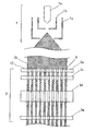
図1は本発明に係るマルチ電子ビーム露光装置の実施例の要部概略図である。図1において、1は、カソード1a、グリッド1b、およびアノード1cよりなる電子銃であって、カソード1aから放射された電子がグリッド1bと、アノード1cの間でクロスオーバー像を形成する。以下、このクロスオーバー像を電子源と記す。
FIG. 1 is a schematic view of the essential portions of an embodiment of a multi-electron beam exposure apparatus according to the present invention. In FIG. 1,
この電子源から放射される電子線は、複数の静電型電子レンズで構成されるコリメータレンズ2によって略平行の電子線となる。略平行な電子線は補正電子光学系3に照射される。
The electron beam emitted from this electron source becomes a substantially parallel electron beam by the
補正電子光学系3は、光軸に沿って、電子銃1側から順に配置された、照射電流検出器3bを含むアパーチャアレイ3a、マルチグリッドアレイ3c、要素電子光学系3d、ブランカーアレイ3e、およびストッパーアレイ3fを備えて構成される。
The correction electron
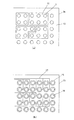
図2にアパーチャアレイ3aの詳細を示す。図2(a)はアパーチャアレイ3aの全体図であり、図2(b)、(c)、および(d)は開口9および照射電流検出器3bの詳細図である。図2(a)に示すように、アパーチャアレイ3aは複数の開口9とそれ以外の遮光部分10からなる。照射電流検出器3bは、アパーチャアレイ3aの各開口9の周囲遮光部分10の表面に形成した照射電子線を集光する電極パッド(検出電極)11(図2(b)および(c)参照)と、照射電流を検出する電流検出手段14(図2(d)参照)で構成される。それぞれの電極パッド11は開口9毎に独立している。即ち、1単位の開口に対し1単位の電極パッド(検出電極)が対応している。図2(c)に示すように、各電極パッド11は、配線基板12に形成された配線13によりアパーチャアレイ3aの外部に引き出される。外部に引き出された各配線13は、各々電流検出手段14に接続される。電流検出手段14の出力は照射電流検出回路101に接続される。配線基板12の開口は、開口9を通過した電子ビームが遮られなければよく、例えば開口9と同心同径でよい。配線基板12の配線はその開口以外の部分を、該開口を避けて通る。
FIG. 2 shows details of the
また、図8(a)に示すように、電極パッド11は複数の開口9を取り囲むように共通としてもよい。即ち、複数の開口毎に1の電極パッド(検出電極)が対応するようにしてもよい。
Further, as shown in FIG. 8A, the
図3にマルチグリッドアレイ3cの詳細を示す。マルチグリッドアレイ3cは、アパーチャアレイ3aで分割された各電子ビームに対応した(アパーチャアレイ3aの各開口9と同軸上に配置した)開口16をもち、各開口16にはグリッド電極(調整電極)15が形成されている。グリッド電極15は円筒電極などを用いることができる。グリッド電極15はそれぞれ個別に電圧を印加できるように配線17が接続される。配線17は、各々個別の印加電圧が設定できるMGA制御回路102(図3(c)参照)の出力に接続される。
FIG. 3 shows details of the
また、図8(b)に示すように、好ましい形態としては、複数のグリッド電極15に対して共通の配線17を接続してもよい。
Further, as shown in FIG. 8B, as a preferable form, a
図1に戻り、マルチグリッドアレイ3cを通過した複数の電子ビームは、要素電子光学系3dにより、電子源の中間像を複数形成する。中間像面には、ブランカーが複数形成されたブランカーアレイ3eが配置されている。
Returning to FIG. 1, the plurality of electron beams that have passed through the
中間像の下流には、2段の対称磁気タブレット・レンズで構成される縮小電子光学系4があり、複数の中間像が露光対象であるウエハ5上に投影される。このときブランカーアレイ3eで偏向された電子ビームは、ストッパーアレイ3fによって遮断されるため、ウエハ5には照射されない。一方、ブランカーアレイ3eで偏向されない電子ビームは、ストッパーアレイ3fで遮断されないため、ウエハ5に照射される。照射電流量は、ブランカーアレイ3eの偏向オンオフ時間を制御することで制御することもできる。
Downstream of the intermediate image, there is a reduction electron
縮小電子光学系4には、要素電子光学系3dからの複数の電子ビームを偏向させて、複数の光源像をウエハ5上でX,Y方向に略同一の変位量だけ変位させる不図示の偏向器が構成されている。この偏向器は、偏向幅が広い場合に用いられる主偏向器と偏向幅が狭い場合に用いられる副偏向器で構成されている。
The reduction electron
また、縮小電子光学系4には、不図示であるが、偏向器を作動させた際に発生する偏向収差による電子源像のフォーカス位置のずれを補正するダイナミックフォーカスコイルと、偏向により発生する偏向収差の非点収差を補正するダイナミックスティグコイルが構成されている。
Although not shown, the reduction electron
θ−Zステージ6は、ウエハ5を搭載し、光軸(Z軸)方向とZ軸回りの回転方向に移動可能なステージであって、ステージ基準板が固設されている。XYステージ7は、θ−Zステージ6を載置し、光軸(Z軸)と直交するXY方向に移動可能なステージである。ファラデーカップ8はステージ上に照射された電子ビームの電流量を検出する。
The θ-
上記の補正電子光学系3を通過する複数の電子ビームは、本発明の補正方法を適用しない状態では、その電流密度が不均一となり、高精度な描画ができない。
The plurality of electron beams that pass through the correction electron
次に、図を用いて本実施例に係るマルチ電子ビーム露光装置に用いられる補正電子光学系の構成要素について説明する。前述したように、補正電子光学系3は、照射電流検出器3bを含むアパーチャアレイ3a、マルチグリッドアレイ3c、要素電子光学系3d、ブランカーアレイ3e、およびストッパーアレイ3fを備えて構成される。
Next, components of the correction electron optical system used in the multi-electron beam exposure apparatus according to the present embodiment will be described with reference to the drawings. As described above, the correction electron
電子銃1は、照射電流量をある値に設定して電子線を出力するが、出力された電子線の強度分布は、照射面内で均一ではなく、電子銃1および露光装置の設置状況等に起因する特定の面分布をもってアパーチャアレイ3aに到達する。アパーチャアレイ3aは、図4に示すように、基板に複数の開口9が形成されている。アパーチャアレイ3aに到達した電子線は、各開口9を通過することにより、複数の電子ビームに分割される。各々の電子ビームは、電子線の照射強度分布にしたがって、それぞれ異なる照射強度すなわち照射電流密度をもつこととなる。
The
次に、図2に示す照射電流検出器3bの動作について説明する。各電子ビームの照射電流を検出する照射電流検出器3bは、アパーチャアレイ3aの各開口9周囲の遮光部分10に形成される電極パッド11と、電極パッド11に照射された電子線の電流量を検出する照射電流検出手段14とで構成される。電極パッド11に照射された電子線の電流密度は、その開口9を通過する電子線の電流密度と略同一と考えてよい。したがって、アパーチャアレイ3aの各開口9周囲の遮光部分10の表面に形成した電極パッド11に照射される電流量を照射電流検出手段14で測定することで、アパーチャアレイ3aの各開口9を通過する電子ビームの電流密度を知ることができる。
Next, the operation of the irradiation
本実施例によれば、照射電流密度の検出にアパーチャアレイ3aの遮光部分10に照射される電子線を利用するので、ウエハに露光する電子ビームは、照射電流密度検出のために遮られることがない。したがって、実露光動作中に各電子ビームの照射電流密度を知ることが可能となる。
According to this embodiment, since the electron beam irradiated to the
また、ひとつの開口9につきひとつの電極パッド11を形成した場合に検出できる電子ビームの照射電流量は極微量であるが、図8に示すように複数の開口9に共通の電極パッド11を形成することで、ひとつの電極パッドあたりの被照射面積が増加し、照射電流検出の精度を向上させることができる。ただし、この場合は複数の開口9の平均電流密度が得られることとなる。
Further, the amount of electron beam irradiation current that can be detected when one
マルチグリッドアレイ3cの電流密度補正動作について、図3を用いて説明する。マルチグリッドアレイ3cは、アパーチャアレイ3aの各開口9に対応するように、複数の電子ビームの光軸と同軸上に開口16が配置されている。マルチグリッドアレイ3cの開口16にはグリッド電極15が形成されており、このグリッド電極15に電子銃1のアノードと同極の電圧を印加すると、開口16を通過する電子線の一部は、グリッド電極15に引き寄せられグリッド電極15に引き込まれる。このときグリッド電極15の印加電圧は電子銃1に対しほとんど影響を与えないので、電子銃1の照射電流量はグリッド電極15への電圧印加により変化しない。したがってグリッド電極15を通過した電子ビームの照射電流密度は通過前よりもグリッド電極15へ引き込まれた分だけ低下する。
The current density correction operation of the
また、引き込み電流量は、グリッド電極15への印加電圧を、ある基準値に対し高くすると増加し(通過電流量は基準値に対し減少)、低くすると減少(通過電流量は基準値に対し増加)する。したがって、電子ビームの照射電流密度はグリッド電極(調整電極)15への印加電圧値によって調整することができる。即ち、調整電極を通過する荷電粒子ビームの量は、調整電極に荷電粒子線源のアノードと同極の電圧を与えることによって調整することができる。
The amount of current drawn increases when the voltage applied to the
また、図8(b)に示すように、複数のグリッド電極15に共通に配線17を接続すると、開口16が多数ある場合、接続配線の省スペース化や制御回路の簡略化などが可能となる。ただし、MGA制御回路102は、共通に接続されたエリアに対応するグリッド電極15に対して共通の電圧を印加する。すなわち、照射電流密度補正の位置分解能が低下することとなる。これに対し、電子ビームの電流密度分布に従って、密度変化の大きい部分は細かく、密度変化の小さいところは広く、エリア分割することで対応することもできる。
Further, as shown in FIG. 8B, when wirings 17 are commonly connected to a plurality of
図4において、要素電子光学系3dは、共通の光軸方向の軸に沿って並ぶ、第一電子光学系アレイの電子レンズと第二電子光学系レンズアレイの電子レンズとでひとつの要素電子光学系3dを構成する。そして、アパーチャアレイ3aが要素電子光学系3dの略前側焦点位置に位置するため、要素電子光学系3dは、分割された複数の電子ビームよりそれぞれの略後側焦点位置に電子源の中間像を形成する。
In FIG. 4, the element electron
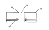
ブランカーアレイ3eは、アパーチャアレイ3aで分割された複数の電子ビームを個別に偏向する偏向手段を一枚の基板上に複数形成したものである。そのひとつの偏向手段の詳細を図5に示す。基板は、開口18と、開口18を挟んだ一対の電極を有して構成され、偏向機能を有するブランキング電極19を形成している。また基板には、ブランキング電極19を個別にオンオフするための配線20が形成されている。
The
図1に示すストッパーアレイ3fは、アパーチャアレイ3aと同様に基板に複数の開口が形成されている。そして、ブランカーアレイ3eで偏向された電子ビームは、その電子ビームに対応したストッパーアレイ3fの開口の外に移動してストッパーアレイ3fを通過しなくなる。
The
次に、本実施例のシステム構成図を図6に示す。CL制御回路100は、コリメータレンズ2の焦点距離を制御する制御回路であり、BLA制御回路104はブランカーアレイ3eのブランキング電極15のオンオフを個別に制御する制御回路である。SLA制御回路103は、要素電子光学系3dを構成する電子レンズの焦点距離を制御する制御回路である。
照射電流検出回路101は照射電流検出器3bからの信号により照射電流量を求める回路である。MGA制御回路102は、マルチグリッドアレイ3cを制御して、各電子ビームの照射電流密度を個別に制御する制御回路である。縮小電子光学系制御回路105は縮小光学系4を制御する制御回路である。ステージ駆動制御回路106は、θ−Zステージ6とXYステージ7を駆動制御する制御回路である。
Next, a system configuration diagram of this embodiment is shown in FIG. The
The irradiation
主制御系110は、描画パターンが記憶されたメモリ111からのデータに基づいて、上記複数の制御回路を制御する。主制御系110はインターフェイス112を介して電子ビーム露光装置全体をコントロールするCPU113によって制御されている。
The
次に、上記のシステム構成における照射電流検出器3bとマルチグリッドアレイ3cを用いた照射電流量補正動作について説明する。
Next, the irradiation current amount correction operation using the irradiation
主制御系110は、照射電流検出回路101で求めた各電子ビームの照射電流量を入力とし、各電子ビームの照射電流量が均一となるように適切な演算を施し、MGA制御回路102に対し各グリッド電極15への印加電圧値を出力する。MGA制御回路102は、主制御系110から出力された印加電圧値に従って、マルチグリッドアレイ3cの各グリッド電極15へ電圧を印加する。その結果、各開口16から照射される電子ビームの照射電流密度が均一になるように補正される。
The
照射電流検出器3bは、実露光動作中に露光電子ビームのウエハへの照射を妨げることなく、照射電流密度を検出できるので、実露光動作中に上記照射電流密度補正を実行することが出来る。
Since the irradiation
次に、図7を用いて本実施例による電子ビーム露光装置の動作について説明する。電子ビーム露光装置によるウエハ5の露光処理のために、主制御系110は図7に示す各ステップを実行する。
Next, the operation of the electron beam exposure apparatus according to this embodiment will be described with reference to FIG. For exposure processing of the
[ステップS1]にて、主制御系110は、アパーチャアレイ3aによって形成される複数の電子ビームのうち、ウエハ5に到達させる一つの電子ビームを選択し、その電子ビームだけがウエハ5を照射するようにBLA制御回路104を制御する。このとき、ステージ駆動制御回路106によってXYステージ7を駆動させ、ウエハ5上に到達するべく選択された電子ビームの近傍にファラデーカップ8を移動させ、選択された電子ビームの電流量を検出する。他の電子ビームについても同様に順次検出し、アパーチャアレイ3aによって形成される複数の電子ビームの全ての照射電流量を記憶する。
In [Step S1], the
[ステップS2]にて、主制御系110は、ステップS1で記憶された全ての電子ビームの照射電流に基づいて、実際にアパーチャアレイ3aに照射される電子線の強度分布を求める。そして、求められた強度分布に基づいて、複数に分割された各電子ビームの照射電流密度が均一になるようにマルチグリッドアレイ3cを調整する。すなわち、MGA制御回路102に命じ、マルチグリッドアレイ3cへの印加電圧値を調整する。
In [Step S2], the
[ステップS3]にて、主制御系110は、ステップS2による調整を終えた状態における、照射電流検出器3bによる照射電流検出結果を基準値として決定し記憶する。すなわち、照射電流検出回路101に命じ、照射電流検出器3bの各検出結果を基準値として記憶する。
In [Step S3], the
[ステップS4]では、ウエハ5をθ−Zステージ6に搬入する。
In [Step S <b> 4], the
[ステップS5]にて、主制御系110は、ウエハ5に対する露光処理を実行する。すなわち、縮小光学系制御回路105に命じ、主偏向器によって、複数の電子ビームを一括して偏向させるとともに、BLA制御回路104に命じ、露光パターンに応じて各電子ビームをオンオフさせ、ウエハ5を露光する。このとき、XYステージ7は連続移動している。
In [Step S5], the
[ステップS6]では、上記露光処理中において、主制御系110は、照射電流検出回路101に命じ、照射電流検出器3bによって照射電流を検出する。
In [Step S6], during the exposure process, the
[ステップS7]にて、主制御系110は、ステップS6において照射電流検出器3bから得られた電流値とステップS3で設定した基準値との差を計算し、これを許容値と比較する。差が許容値を超えている場合は、電子ビームの照射電流密度分布に許容範囲を超える不均一さが発生しているものと判断する。よって処理はステップS8へ進み、電子ビームの照射電流密度分布が均一になるように再調整を行なう。一方、差が許容値を超えていなければ、ステップS9に進み、露光処理を継続する。
In [Step S7], the
[ステップS8]にて、主制御系110は、露光処理を停止し、照射電流検出器3bで検出される電子ビームの照射電流が基準値になるようにマルチグリッドアレイ3cを調整する。すなわち、MGA制御回路102に命じ、マルチグリッドアレイ3cへの印加電圧値を調整する。照射電流検出器3bの測定結果が基準値になるようにマルチグリッドアレイ3cを調整すれば、実際にアパーチャアレイ3aに照射される電子ビームの照射電流密度分布は元のように(ステップS2で調整された時点のように)一様なものとなる。なお、露光処理の停止は、ブランカーアレイ3eで複数の電子ビームの全部を偏向することにより、ウエハ5に電子ビームが到達しないようにする。
In [Step S8], the
[ステップS9]では、ウエハ5の全面について露光を完了したかどうか判断し、完了していなければステップS5へ戻る。完了していれば、ステップS10へ進む。
In [Step S9], it is determined whether or not the exposure has been completed for the entire surface of the
[ステップS10]では、ウエハ5をθ−Zステージ6から搬出し、本処理を終了する。本実施例では、電子ビームの照射電流が基準値になるようにマルチグリッドアレイ3cを調整しているが、ウエハ5を露光する際、ブランカーアレイ3eのオンオフ時間制御により、各電子ビームの照射時間を調整して、ウエハ5に照射される電流の積分値を許容値内にしてもかまわない。あるいはマルチグリッドアレイ3cおよびブランカーアレイ3eを併用してもかまわない。
In [Step S10], the
以上説明したように本実施例によれば、照射電流検出器3bによって、アパーチャアレイ3aを照射する電子ビームのうち、ウエハ5の露光に用いない部分(遮光部分10)の電流量を検出することにより、露光中の電子ビームの照射電流密度分布を評価することができる。そして、この評価結果に基づいてマルチグリッドアレイ3cを制御してウエハ5を露光する電子ビームの照射電流密度分布を均一にする。このため、露光する複数の電子ビームの照射電流量を均一に保つことができ、高精度に露光を行うことができる。
As described above, according to the present embodiment, the irradiation
次に、本発明の実施例2として、上記実施例1に係る露光装置を利用した半導体デバイスの製造プロセスを説明する。図9は半導体デバイスの全体的な製造プロセスのフローを示す図である。ステップ11(回路設計)では半導体デバイスの回路設計を行う。ステップ12(EBデータ変換)では設計した回路パターンに基づいて露光装置の露光制御データを作成する。 Next, as a second embodiment of the present invention, a semiconductor device manufacturing process using the exposure apparatus according to the first embodiment will be described. FIG. 9 is a diagram showing a flow of an entire manufacturing process of a semiconductor device. In step 11 (circuit design), a semiconductor device circuit is designed. In step 12 (EB data conversion), exposure control data for the exposure apparatus is created based on the designed circuit pattern.
一方、ステップ13(ウエハ製造)ではシリコン等の材料を用いてウエハを製造する。ステップ14(ウエハプロセス)は前工程と呼ばれ、上記露光制御データが入力された露光装置とウエハを用い、リソグラフィ技術を利用してウエハ上に実際の回路を形成する。次のステップ15(組み立て)は後工程と呼ばれ、ステップ14によって作製されたウエハを用いて半導体チップ化する工程であり、アッセンブリ工程(ダイシング、ボンディング)、パッケージング工程(チップ封入)等の組み立て工程を含む。ステップ16(検査)ではステップ15で作製された半導体デバイスの動作確認テスト、耐久性テスト等の検査を行う。こうした工程を経て半導体デバイスが完成し、ステップ17でこれを出荷する。
On the other hand, in step 13 (wafer manufacture), a wafer is manufactured using a material such as silicon. Step 14 (wafer process) is called a pre-process, and an actual circuit is formed on the wafer using lithography using the exposure apparatus and wafer to which the exposure control data has been input. The next step 15 (assembly) is called a post-process, and is a process for forming a semiconductor chip using the wafer produced in
上記ステップ14のウエハプロセスは以下のステップを有する。ウエハの表面を酸化させる酸化ステップ、ウエハ表面に絶縁膜を成膜するCVDステップ、ウエハ上に電極を蒸着によって形成する電極形成ステップ、ウエハにイオンを打ち込むイオン打ち込みステップ、ウエハに感光剤を塗布するレジスト処理ステップ、上記の露光装置によって回路パターンをレジスト処理ステップ後のウエハに焼付け露光する露光ステップ、露光ステップで露光したウエハを現像する現像ステップ、現像ステップで現像したレジスト像以外の部分を削り取るエッチングステップ、エッチングが済んで不要となったレジストを取り除くレジスト剥離ステップ。これらのステップを繰り返し行うことによって、ウエハ上に多重に回路パターンを形成する。
The wafer process in
1:電子銃、1a:カソード、1b:グリッド、1c:アノード、2:コリメータレンズ、3:補正電子光学系、3a:アパーチャアレイ、3b:照射電流検出器、3c:マルチグリッドアレイ、3d:要素電子光学系、3e:ブランカーアレイ、3f:ストッパーアレイ、4:縮小電子光学系、5:ウエハ、6:θ−Zステージ、7:XYステージ、8:ファラデーカップ、9:アパーチャアレイの開口、10:遮光部分、11:電極パッド(検出電極)、12:配線基板、13:照射電流検出器の配線、14:照射電流検出手段、15:グリッド電極(調整電極)、16:マルチグリッドアレイの開口、17:マルチグリッドアレイの配線、18:ブランカーアレイの開口、19:ブランキング電極、20:ブランカーアレイの配線、100:CL制御回路、101:照射電流検出回路、102:MGA制御回路、103:SLA制御回路、104:BLA制御回路、105:縮小光学系制御回路、106:ステージ駆動制御回路、110:主制御系、111:メモリ、112:インターフェイス、113:CPU。
1: electron gun, 1a: cathode, 1b: grid, 1c: anode, 2: collimator lens, 3: correction electron optical system, 3a: aperture array, 3b: irradiation current detector, 3c: multigrid array, 3d: element Electron optical system, 3e: Blanker array, 3f: Stopper array, 4: Reduction electron optical system, 5: Wafer, 6: θ-Z stage, 7: XY stage, 8: Faraday cup, 9: Aperture array aperture, 10 : Light shielding part, 11: electrode pad (detection electrode), 12: wiring board, 13: wiring of irradiation current detector, 14: irradiation current detection means, 15: grid electrode (adjustment electrode), 16: opening of multigrid array 17: Wiring of multi-grid array, 18: Opening of blanker array, 19: Blanking electrode, 20: Wiring of blanker array, 1 0: CL control circuit 101: Irradiation current detection circuit 102: MGA control circuit 103: SLA control circuit 104: BLA control circuit 105: Reduction optical system control circuit 106: Stage drive control circuit 110:
Claims (5)
前記アパーチャアレイの開口を通過する前記荷電粒子ビームの強度を検出する検出手段と、
前記検出手段の検出結果に基づいて前記荷電粒子ビームの強度を調整する調整手段と、を備え、
前記調整手段は、グリッドアレイ上の複数の開口に形成された複数のグリッド電極を有し、前記グリッド電極に前記荷電粒子線源のアノードと同極の電圧を印加することで、前記荷電粒子ビームの強度を調整することを特徴とする荷電粒子線露光装置。 In a charged particle beam exposure apparatus that divides a charged particle beam from a charged particle beam source into a plurality of charged particle beams at a plurality of openings provided in an aperture array and performs exposure using the plurality of charged particle beams,
A detecting means for detecting the intensity of the previous SL charged particle beam passing through the aperture of the aperture array,
Adjusting means for adjusting the intensity of the charged particle beam based on the detection result of the detection means ,
The adjusting means has a plurality of grid electrodes formed in a plurality of openings on the grid array, and applies a voltage having the same polarity as the anode of the charged particle beam source to the grid electrodes, whereby the charged particle beam The charged particle beam exposure apparatus characterized by adjusting the intensity of the .
前記調整手段は、前記複数のグリッド電極毎に、前記荷電粒子ビームの強度を調整することを特徴とする請求項1に記載の荷電粒子線露光装置。 The detection means detects the intensity of the charged particle beam for each of the plurality of openings on the aperture array ,
The charged particle beam exposure apparatus according to claim 1, wherein the adjusting unit adjusts the intensity of the charged particle beam for each of the plurality of grid electrodes .
前記調整手段は、前記複数のグリッド電極のうちグループ分けされたグリッド電極群毎に、前記荷電粒子ビームの強度を調整することを特徴とする請求項1に記載の荷電粒子線露光装置。 It said detecting means, each aperture group grouped among the plurality of apertures on the aperture array, detects the intensity of the charged particle beam,
The charged particle beam exposure apparatus according to claim 1, wherein the adjusting unit adjusts the intensity of the charged particle beam for each group of grid electrodes grouped among the plurality of grid electrodes .
前記アパーチャアレイの開口を通過する前記荷電粒子ビームの強度を検出する検出工程と、
前記検出工程での検出結果に基づいて前記荷電粒子ビームの強度を調整する調整工程と、を有し、
前記調整工程では、グリッドアレイ上の複数の開口に形成された複数のグリッド電極に、前記荷電粒子線源のアノードと同極の電圧を印加することで前記荷電粒子ビームの強度を調整することを特徴とする露光方法。 The charged particle beam from the charged particle beam source is divided into a plurality of charged particle beams in a plurality of apertures provided in the aperture array, the exposure light method of performing exposure using a plurality of charged particle beams,
A detection step of detecting the intensity of the previous SL charged particle beam passing through the aperture of the aperture array,
Have a, an adjustment step of adjusting the intensity of the charged particle beam based on the detection result of the higher the detection Engineering,
In the adjusting step, the intensity of the charged particle beam is adjusted by applying a voltage having the same polarity as the anode of the charged particle beam source to a plurality of grid electrodes formed in a plurality of openings on the grid array. A featured exposure method.
Priority Applications (2)
| Application Number | Priority Date | Filing Date | Title |
|---|---|---|---|
| JP2004378665A JP4612838B2 (en) | 2004-12-28 | 2004-12-28 | Charged particle beam exposure apparatus and exposure method therefor |
| US11/315,303 US7388214B2 (en) | 2004-12-28 | 2005-12-23 | Charged-particle beam exposure apparatus and method |
Applications Claiming Priority (1)
| Application Number | Priority Date | Filing Date | Title |
|---|---|---|---|
| JP2004378665A JP4612838B2 (en) | 2004-12-28 | 2004-12-28 | Charged particle beam exposure apparatus and exposure method therefor |
Publications (3)
| Publication Number | Publication Date |
|---|---|
| JP2006186125A JP2006186125A (en) | 2006-07-13 |
| JP2006186125A5 JP2006186125A5 (en) | 2008-02-28 |
| JP4612838B2 true JP4612838B2 (en) | 2011-01-12 |
Family
ID=36610326
Family Applications (1)
| Application Number | Title | Priority Date | Filing Date |
|---|---|---|---|
| JP2004378665A Expired - Fee Related JP4612838B2 (en) | 2004-12-28 | 2004-12-28 | Charged particle beam exposure apparatus and exposure method therefor |
Country Status (2)
| Country | Link |
|---|---|
| US (1) | US7388214B2 (en) |
| JP (1) | JP4612838B2 (en) |
Families Citing this family (16)
| Publication number | Priority date | Publication date | Assignee | Title |
|---|---|---|---|---|
| JP2008066359A (en) * | 2006-09-05 | 2008-03-21 | Canon Inc | Charged particle beam lens array, exposure apparatus and method of manufacturing device |
| US8481962B2 (en) * | 2010-08-10 | 2013-07-09 | Fei Company | Distributed potential charged particle detector |
| JP5576332B2 (en) * | 2011-04-06 | 2014-08-20 | 株式会社アドバンテスト | Electron beam exposure apparatus and electron beam exposure method |
| WO2012144904A2 (en) | 2011-04-22 | 2012-10-26 | Mapper Lithography Ip B.V. | Position determination in a lithography system using a substrate having a partially reflective position mark |
| KR20140027298A (en) | 2011-04-22 | 2014-03-06 | 마퍼 리쏘그라피 아이피 비.브이. | Lithography system for processing a target, such as a wafer, and a method for operating a lithography system for processing a target, such as a wafer |
| JP5932023B2 (en) | 2011-05-13 | 2016-06-08 | マッパー・リソグラフィー・アイピー・ビー.ブイ. | Lithographic system for processing at least part of a target |
| JP5956797B2 (en) | 2012-03-22 | 2016-07-27 | 株式会社ニューフレアテクノロジー | Multi-charged particle beam writing apparatus and multi-charged particle beam writing method |
| JP5977550B2 (en) * | 2012-03-22 | 2016-08-24 | 株式会社ニューフレアテクノロジー | Multi charged particle beam lithography system |
| JPWO2014156170A1 (en) * | 2013-03-29 | 2017-02-16 | 国立大学法人東北大学 | Electron beam irradiation device |
| JP2014229841A (en) * | 2013-05-24 | 2014-12-08 | キヤノン株式会社 | Drawing device and method of manufacturing article |
| JP2018078250A (en) | 2016-11-11 | 2018-05-17 | 株式会社ニューフレアテクノロジー | Multi-charged particle beam lithography device |
| IL277822B1 (en) | 2018-05-01 | 2024-04-01 | Asml Netherlands Bv | Multi-beam inspection apparatus |
| US11393658B2 (en) * | 2018-11-13 | 2022-07-19 | Hitachi High-Tech Corporation | Charged particle beam apparatus and sample observation method |
| EP3716313A1 (en) * | 2019-03-28 | 2020-09-30 | ASML Netherlands B.V. | Aperture array with integrated current measurement |
| KR20220002554A (en) * | 2019-05-28 | 2022-01-06 | 에이에스엠엘 네델란즈 비.브이. | Multiple Charged-Particle Beam Devices with Low Crosstalk |
| DE102021118561B4 (en) | 2021-07-19 | 2023-03-30 | Carl Zeiss Multisem Gmbh | Method for operating a multi-beam particle microscope with fast beam current control, computer program product and multi-beam particle microscope |
Citations (3)
| Publication number | Priority date | Publication date | Assignee | Title |
|---|---|---|---|---|
| JPH0557754U (en) * | 1992-01-10 | 1993-07-30 | 日新電機株式会社 | Beam current measuring device |
| JP2004193516A (en) * | 2002-12-13 | 2004-07-08 | Canon Inc | Charged-particle beam exposure apparatus, and control method thereof |
| JP2004288577A (en) * | 2003-03-25 | 2004-10-14 | Nikon Corp | Electron gun, controlling method for electron gun and electron beam exposure equipment |
Family Cites Families (2)
| Publication number | Priority date | Publication date | Assignee | Title |
|---|---|---|---|---|
| JP2001006589A (en) * | 1999-06-24 | 2001-01-12 | Nikon Corp | Manufacture of electron gun, electron beam exposure device and semiconductor device |
| JP3471774B2 (en) | 2001-08-06 | 2003-12-02 | 株式会社日立製作所 | Electron beam drawing apparatus and method |
-
2004
- 2004-12-28 JP JP2004378665A patent/JP4612838B2/en not_active Expired - Fee Related
-
2005
- 2005-12-23 US US11/315,303 patent/US7388214B2/en not_active Expired - Fee Related
Patent Citations (3)
| Publication number | Priority date | Publication date | Assignee | Title |
|---|---|---|---|---|
| JPH0557754U (en) * | 1992-01-10 | 1993-07-30 | 日新電機株式会社 | Beam current measuring device |
| JP2004193516A (en) * | 2002-12-13 | 2004-07-08 | Canon Inc | Charged-particle beam exposure apparatus, and control method thereof |
| JP2004288577A (en) * | 2003-03-25 | 2004-10-14 | Nikon Corp | Electron gun, controlling method for electron gun and electron beam exposure equipment |
Also Published As
| Publication number | Publication date |
|---|---|
| JP2006186125A (en) | 2006-07-13 |
| US20060138359A1 (en) | 2006-06-29 |
| US7388214B2 (en) | 2008-06-17 |
Similar Documents
| Publication | Publication Date | Title |
|---|---|---|
| US7388214B2 (en) | Charged-particle beam exposure apparatus and method | |
| US6903353B2 (en) | Charged particle beam exposure apparatus, device manufacturing method, and charged particle beam applied apparatus | |
| US6137113A (en) | Electron beam exposure method and apparatus | |
| JP4327497B2 (en) | Electron beam exposure apparatus, electron beam exposure method, semiconductor element manufacturing method, mask, and mask manufacturing method | |
| JP2005056923A (en) | Multi-charged particle beam optical lithography system and method, and method for manufacturing device employing the system or the method | |
| US6274877B1 (en) | Electron beam exposure apparatus | |
| TWI712067B (en) | Data processing method, data processing device and multi-charged particle beam drawing device | |
| JP7180515B2 (en) | Multi-charged particle beam writing apparatus and multi-charged particle beam writing method | |
| US7041988B2 (en) | Electron beam exposure apparatus and electron beam processing apparatus | |
| EP2388801B1 (en) | Multi-column electron beam lithography system and electron beam orbit adjusting method thereof | |
| US7173262B2 (en) | Charged particle beam exposure apparatus, charged particle beam exposure method and device manufacturing method | |
| JP4368411B2 (en) | Electron beam exposure system | |
| US8829461B2 (en) | Scanning apparatus, drawing apparatus, and method of manufacturing article | |
| US7005659B2 (en) | Charged particle beam exposure apparatus, charged particle beam exposure method, and device manufacturing method using the same apparatus | |
| US20050006603A1 (en) | Charged particle beam exposure method, charged particle beam exposure apparatus, and device manufacturing method | |
| JP4804136B2 (en) | Charged particle beam apparatus and device manufacturing method | |
| JP2015035563A (en) | Drawing data generation method, processing device, program, drawing device and article manufacturing method | |
| US20150362842A1 (en) | Lithography apparatus, and method of manufacturing article | |
| JP3976835B2 (en) | Electron beam exposure method and electron beam exposure apparatus | |
| US6277531B1 (en) | Charged-particle-beam microlithography apparatus and methods including focal-point correction | |
| JP4356064B2 (en) | Charged particle beam exposure apparatus and device manufacturing method using the apparatus | |
| JP7176480B2 (en) | Multi-charged particle beam writing method and multi-charged particle beam writing apparatus | |
| JP4494734B2 (en) | Charged particle beam drawing method, charged particle beam exposure apparatus, and device manufacturing method | |
| JP2004165498A (en) | Charged particle beam optical lithography system, method for fabricating device | |
| JP2007251024A (en) | Charged beam exposure apparatus, charged beam exposure method, and method of manufacturing semiconductor device |
Legal Events
| Date | Code | Title | Description |
|---|---|---|---|
| A521 | Request for written amendment filed |
Free format text: JAPANESE INTERMEDIATE CODE: A523 Effective date: 20071225 |
|
| A621 | Written request for application examination |
Free format text: JAPANESE INTERMEDIATE CODE: A621 Effective date: 20071225 |
|
| A521 | Request for written amendment filed |
Free format text: JAPANESE INTERMEDIATE CODE: A523 Effective date: 20080123 |
|
| RD01 | Notification of change of attorney |
Free format text: JAPANESE INTERMEDIATE CODE: A7421 Effective date: 20090406 |
|
| RD04 | Notification of resignation of power of attorney |
Free format text: JAPANESE INTERMEDIATE CODE: A7424 Effective date: 20100201 |
|
| A977 | Report on retrieval |
Free format text: JAPANESE INTERMEDIATE CODE: A971007 Effective date: 20100624 |
|
| A131 | Notification of reasons for refusal |
Free format text: JAPANESE INTERMEDIATE CODE: A131 Effective date: 20100629 |
|
| RD01 | Notification of change of attorney |
Free format text: JAPANESE INTERMEDIATE CODE: A7421 Effective date: 20100630 |
|
| A521 | Request for written amendment filed |
Free format text: JAPANESE INTERMEDIATE CODE: A523 Effective date: 20100824 |
|
| TRDD | Decision of grant or rejection written | ||
| A01 | Written decision to grant a patent or to grant a registration (utility model) |
Free format text: JAPANESE INTERMEDIATE CODE: A01 Effective date: 20101012 |
|
| A01 | Written decision to grant a patent or to grant a registration (utility model) |
Free format text: JAPANESE INTERMEDIATE CODE: A01 |
|
| A61 | First payment of annual fees (during grant procedure) |
Free format text: JAPANESE INTERMEDIATE CODE: A61 Effective date: 20101016 |
|
| FPAY | Renewal fee payment (event date is renewal date of database) |
Free format text: PAYMENT UNTIL: 20131022 Year of fee payment: 3 |
|
| R150 | Certificate of patent or registration of utility model |
Free format text: JAPANESE INTERMEDIATE CODE: R150 |
|
| LAPS | Cancellation because of no payment of annual fees |