JP7176480B2 - Multi-charged particle beam writing method and multi-charged particle beam writing apparatus - Google Patents
Multi-charged particle beam writing method and multi-charged particle beam writing apparatus Download PDFInfo
- Publication number
- JP7176480B2 JP7176480B2 JP2019111319A JP2019111319A JP7176480B2 JP 7176480 B2 JP7176480 B2 JP 7176480B2 JP 2019111319 A JP2019111319 A JP 2019111319A JP 2019111319 A JP2019111319 A JP 2019111319A JP 7176480 B2 JP7176480 B2 JP 7176480B2
- Authority
- JP
- Japan
- Prior art keywords
- amount
- beams
- charged particle
- focal position
- positional deviation
- Prior art date
- Legal status (The legal status is an assumption and is not a legal conclusion. Google has not performed a legal analysis and makes no representation as to the accuracy of the status listed.)
- Active
Links
Images


Description
本発明は、マルチ荷電粒子ビーム描画方法及びマルチ荷電粒子ビーム描画装置に関する。 The present invention relates to a multi-charged particle beam writing method and a multi-charged particle beam writing apparatus.
LSIの高集積化に伴い、半導体デバイスに要求される回路線幅は年々微細化されてきている。半導体デバイスへ所望の回路パターンを形成するためには、縮小投影型露光装置を用いて、石英上に形成された高精度の原画パターン(マスク、或いは特にステッパやスキャナで用いられるものはレチクルともいう。)をウェーハ上に縮小転写する手法が採用されている。高精度の原画パターンは、電子ビーム描画装置によって描画され、所謂、電子ビームリソグラフィ技術が用いられている。 2. Description of the Related Art As LSIs become highly integrated, circuit line widths required for semiconductor devices are becoming finer year by year. In order to form a desired circuit pattern on a semiconductor device, a reduction projection type exposure apparatus is used to form a highly accurate original image pattern (a mask, or a reticle for those used particularly in steppers and scanners) formed on quartz. ) is transferred onto the wafer in a reduced size. A high-precision original image pattern is drawn by an electron beam drawing apparatus using a so-called electron beam lithography technique.
マルチビームを使った描画装置は、1本の電子ビームで描画する場合に比べて、一度に多くのビームを照射できるので、スループットを大幅に向上させることができる。マルチビーム方式の描画装置では、例えば、電子銃から放出された電子ビームを複数の開口を持った成形アパーチャ部材に通してマルチビームを形成し、ブランキングプレートで各ビームのブランキング制御を行い、遮蔽されなかった各ビームが光学系で縮小され、ステージ上に載置された基板に照射される。 A drawing apparatus using multi-beams can irradiate many beams at once, compared with the case of writing with a single electron beam, so that the throughput can be greatly improved. In a multi-beam drawing apparatus, for example, electron beams emitted from an electron gun are passed through a shaping aperture member having a plurality of openings to form multi-beams, blanking control of each beam is performed by a blanking plate, Each unshielded beam is demagnified by an optical system and applied to the substrate placed on the stage.
ブランキングプレートには、マルチビームの各ビームに対応する複数のブランカが設けられている。各ブランカが所定の電圧を印加することで、ビームを個別にオンオフ制御することができる。各ビームは、周辺のビームに対応するブランカからの漏れ電場(クロストーク)により、ビーム進行方向がずれる、いわゆる「出射角異常」が生じることがあった。また、ブランキングプレートの製作精度不良に伴うビーム散乱によっても出射角異常が生じることがあった。 A blanking plate is provided with a plurality of blankers corresponding to each beam of the multi-beam. By applying a predetermined voltage to each blanker, the beams can be individually controlled on and off. Each beam sometimes has a so-called "exit angle anomaly" in which the beam traveling direction deviates due to a leakage electric field (crosstalk) from blankers corresponding to surrounding beams. In addition, beam scattering due to poor manufacturing accuracy of the blanking plate may also cause an output angle abnormality.
マルチビーム描画では、焦点合わせ等の光学系の調整が重要である。従来、対物レンズで焦点位置を変えながら、ステージ上のライン状の反射マークをスキャンして反射電子を検出し、各焦点位置で得られたプロファイルに基づいて焦点合わせを行っていた。反射マークと基板との高さの違いによる焦点位置のずれは、ステージ高さを調整することで補正していた。また、基板の表面高さをグリッド状に取得し、多項式フィッティングして、基板の撓みによる焦点位置のずれを補正していた。しかし、ビーム電流によるクーロン効果の影響や、多項式で求まる基板表面高さの誤差により、焦点位置を補正しきれないことがあった。 In multi-beam writing, adjustment of the optical system such as focusing is important. Conventionally, while changing the focal position with an objective lens, a line-shaped reflective mark on the stage is scanned to detect backscattered electrons, and focusing is performed based on the profile obtained at each focal position. The deviation of the focus position due to the height difference between the reflection mark and the substrate was corrected by adjusting the height of the stage. Further, the surface height of the substrate is obtained in a grid pattern, and polynomial fitting is performed to correct the deviation of the focus position due to the bending of the substrate. However, due to the influence of the Coulomb effect due to the beam current and the error of the substrate surface height determined by the polynomial, the focal position could not be corrected in some cases.
焦点位置の補正残差が大きい場合、上述した出射角異常により、基板上でのビーム照射位置がずれ、描画精度を劣化させることがあった。 When the correction residual error of the focus position is large, the beam irradiation position on the substrate is shifted due to the above-described output angle abnormality, and the writing accuracy is degraded.
本発明は、ビーム照射位置のずれを低減し、描画精度を向上させるマルチ荷電粒子ビーム描画方法及びマルチ荷電粒子ビーム描画装置を提供することを課題とする。 SUMMARY OF THE INVENTION It is an object of the present invention to provide a multi-charged particle beam writing method and a multi-charged particle beam writing apparatus that reduce deviations in beam irradiation positions and improve writing accuracy.
本発明の一態様によるマルチ荷電粒子ビーム描画方法は、荷電粒子ビームを放出する工程と、成形アパーチャアレイ基板に設けられた複数の開口を前記荷電粒子ビームが通過することによりマルチビームを形成する工程と、前記マルチビームの各ビームに対応するブランカが設けられたブランキングプレートを用いて、各ビームのオンオフを切り替える工程と、前記マルチビームの焦点位置の変動量を算出する工程と、予め求められた焦点位置と前記マルチビームの各ビームの位置ずれ量との相関関係に基づき、算出された前記焦点位置より前記位置ずれ量を算出する工程と、前記位置ずれ量に基づいて、前記マルチビームの各ビームの照射量を変調する工程と、変調後の照射量で前記マルチビームを基板に照射してパターンを描画する工程と、を備えるものである。 A multi-charged particle beam writing method according to an aspect of the present invention comprises the steps of: emitting charged particle beams; and forming multi-beams by causing the charged particle beams to pass through a plurality of openings provided in a shaping aperture array substrate. a step of switching on and off each beam using a blanking plate provided with a blanker corresponding to each beam of the multi-beam; a step of calculating a variation amount of the focus position of the multi-beam; calculating the amount of positional deviation from the calculated focal position based on the correlation between the focal position and the amount of positional deviation of each beam of the multi-beam; The method comprises a step of modulating the dose of each beam, and a step of irradiating the substrate with the multi-beams with the modulated dose to draw a pattern.
本発明の一態様では、前記相関関係は、ショット毎、またはマルチビームを複数のビームに分割したブロック毎に求められる。 In one aspect of the present invention, the correlation is obtained for each shot or for each block obtained by dividing a multi-beam into a plurality of beams.
本発明の一態様では、前記変調後の前記マルチビームの焦点位置の変動量又は前記位置ずれ量が所定値以下となるまで、前記マルチビームの各ビームの照射量を変調する工程を繰り返し行う。 In one aspect of the present invention, the step of modulating the irradiation amount of each beam of the multi-beams is repeated until the amount of change in the focal position of the multi-beams after the modulation or the amount of positional deviation is equal to or less than a predetermined value.
本発明の一態様では、前記マルチビームの焦点位置の変動量は、前記マルチビームの各ビームの照射量を変調することによる前記マルチビームの焦点位置の変動量を含む。 In one aspect of the present invention, the amount of change in the focal position of the multibeam includes the amount of change in the focal position of the multibeam due to modulation of the irradiation amount of each beam of the multibeam.
本発明の一態様によるマルチ荷電粒子ビーム描画装置は、荷電粒子ビームを放出する放出部と、複数の開口が形成され、前記複数の開口を前記荷電粒子ビームが通過することによりマルチビームを形成する成形アパーチャアレイ基板と、前記マルチビームの各ビームにそれぞれ対応し、ビームのオンオフを切り替える複数のブランカが配置されたブランキングプレートと、前記マルチビームの焦点位置の変動量を算出し、予め求められた焦点位置と前記マルチビームの各ビームの位置ずれ量との相関関係に基づき、算出された前記焦点位置より前記位置ずれ量を算出し、前記位置ずれ量に基づいて、各ビームの照射量を変調する制御計算機と、変調後の照射量に基づいて前記複数のブランカを制御する偏向制御回路と、を備えるものである。 A multi-charged particle beam drawing apparatus according to an aspect of the present invention includes an emission unit that emits charged particle beams, and a plurality of openings, and the charged particle beams pass through the plurality of openings to form multi-beams. A shaping aperture array substrate, a blanking plate on which a plurality of blankers for switching the beams on and off corresponding to each beam of the multi-beam are arranged, and a variation amount of the focal position of the multi-beam are calculated and obtained in advance. The amount of positional deviation is calculated from the calculated focal position based on the correlation between the focal position and the amount of positional deviation of each beam of the multi-beam, and the irradiation amount of each beam is calculated based on the amount of positional deviation. A control computer for modulation and a deflection control circuit for controlling the plurality of blankers based on the modulated dose.
本発明によれば、ビーム照射位置のずれを低減し、描画精度を向上させることができる。 According to the present invention, it is possible to reduce the deviation of the beam irradiation position and improve the writing accuracy.
以下、本発明の実施の形態を図面に基づいて説明する。実施の形態では、荷電粒子ビームの一例として、電子ビームを用いた構成について説明する。但し、荷電粒子ビームは電子ビームに限るものでなく、イオンビーム等でもよい。 BEST MODE FOR CARRYING OUT THE INVENTION Hereinafter, embodiments of the present invention will be described with reference to the drawings. In the embodiment, a configuration using an electron beam as an example of a charged particle beam will be described. However, the charged particle beam is not limited to the electron beam, and may be an ion beam or the like.
図1は、本実施形態における描画装置の構成を示す概念図である。図1において、描画装置は、描画部1と制御部100を備えている。描画装置は、マルチ荷電粒子ビーム描画装置の一例である。描画部1は、電子鏡筒2と描画室20を備えている。電子鏡筒2内には、電子銃4、照明レンズ6、成形アパーチャアレイ基板8、ブランキングプレート10、縮小レンズ12、制限アパーチャ部材14、対物レンズ15、コイル16、主偏向器17(偏向器)、及び副偏向器(図示略)が配置されている。
FIG. 1 is a conceptual diagram showing the configuration of a drawing apparatus according to this embodiment. In FIG. 1 , the drawing apparatus includes a
描画室20内には、XYステージ22が配置される。XYステージ22上には、描画対象となる基板70が配置される。基板70には、半導体装置を製造する際の露光用マスク、或いは、半導体装置が製造される半導体基板(シリコンウェハ)等が含まれる。また、基板70には、レジストが塗布された、まだ何も描画されていないマスクブランクスが含まれる。
An
XYステージ22上には、XYステージ22の位置測定用のミラー24が配置される。
A
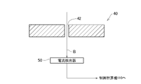
また、XYステージ22には、基板70が載置される位置とは異なる位置に、位置検出用のマークが配置されている。マークは特に限定されないが、例えば透過型のマークであるマルチビーム検査用アパーチャ40(以下、「検査アパーチャ40」と記載する)を用いることができる。検査アパーチャ40は、さらに電流検出器50を有するマルチビーム用ビーム検査装置を構成する。検査アパーチャ40は、調整機構(図示略)により高さが調整可能となっている。検査アパーチャ40は、基板70と同じ高さ位置に設置されることが好ましい。
Further, on the
図2はマルチビーム用ビーム検査装置の概略構成図である。検査アパーチャ40は、電子ビームが1本だけ通過するように制限するものである。検査アパーチャ40は例えば円形の平面形状をなし、中心軸に沿って1本のビームが通過する貫通孔42が形成されている。
FIG. 2 is a schematic configuration diagram of a multi-beam beam inspection apparatus.
貫通孔42を通過した電子ビームBは、電流検出器50に入射し、ビーム電流が検出される。電流検出器50には、例えばSSD(半導体検出器(solid-state detector))を用いることができる。電流検出器50による検出結果は制御計算機110に通知される。
The electron beam B that has passed through the through
制御部100は、制御計算機110、偏向制御回路130、デジタル・アナログ変換(DAC)アンプ131、コイル制御回路132、レンズ制御回路133、ステージ位置検出器135、及び磁気ディスク装置等の記憶装置140,142,144を有している。
The
偏向制御回路130、コイル制御回路132、レンズ制御回路133、ステージ位置検出器135、及び記憶装置140は、バスを介して制御計算機110に接続されている。記憶装置140には、描画データが外部から入力され、格納されている。
The
偏向制御回路130には、DACアンプ131が接続される。DACアンプ131は主偏向器17に接続される。コイル制御回路132には、コイル16が接続されている。レンズ制御回路133には、対物レンズ15が接続されている。
A
制御計算機110は、ビーム位置ずれ量算出部111、焦点位置算出部112、面積率算出部113、照射量算出部114、照射量変調部115、判定部116及び描画制御部117を備える。制御計算機110の各部の機能は、ハードウェアで実現されてもよいし、ソフトウェアで実現されてもよい。ソフトウェアで構成する場合には、制御計算機110の少なくとも一部の機能を実現するプログラムを記録媒体に収納し、電気回路を含むコンピュータに読み込ませて実行させてもよい。記録媒体は、磁気ディスクや光ディスク等の着脱可能なものに限定されず、ハードディスク装置やメモリなどの固定型の記録媒体でもよい。
The
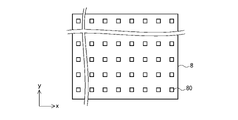
図3は、成形アパーチャアレイ基板8の構成を示す概念図である。図3に示すように、成形アパーチャアレイ基板8には、縦(y方向)m列×横(x方向)n列(m,n≧2)の開口80が所定の配列ピッチでマトリクス状に形成されている。各開口80は、共に同じ寸法形状の矩形で形成される。或いは、同じ径の円形であっても構わない。
FIG. 3 is a conceptual diagram showing the configuration of the shaping
電子銃4から放出された電子ビーム30は、照明レンズ6によりほぼ垂直に成形アパーチャアレイ基板8全体を照明する。電子ビーム30は、成形アパーチャアレイ基板8のすべての開口80が含まれる領域を照明する。これらの複数の開口80を電子ビーム30の一部がそれぞれ通過することで、図1に示すようなマルチビーム30a~30eが形成されることになる。
An
ブランキングプレート10には、図3に示した成形アパーチャアレイ基板8の各開口80に対応する位置にマルチビームの各ビームが通過する通過孔(開口部)が形成されている。各通過孔の近傍には、ビームを偏向するブランキング偏向用の電極(ブランカ:ブランキング偏向器)が配置されている。
The blanking
各通過孔を通過するマルチビーム30a~30eを構成する各電子ビームは、それぞれ独立に、ブランカから印加される電圧によって偏向される。この偏向によってブランキング制御が行われる。このように、複数のブランカが、成形アパーチャアレイ基板8の複数の開口80を通過したマルチビームのうち、それぞれ対応するビームのブランキング偏向を行う。
Each electron beam that constitutes the multi-beams 30a to 30e passing through each passage hole is independently deflected by a voltage applied from a blanker. Blanking control is performed by this deflection. In this manner, the plurality of blankers perform blanking deflection of corresponding beams among the multi-beams that have passed through the plurality of
ブランキングプレート10を通過したマルチビーム30a~30eは、縮小レンズ12によって、各々のビームサイズと配列ピッチが縮小され、制限アパーチャ部材14に形成された中心の穴に向かって進む。ブランキングプレート10のブランカにより偏向された電子ビームは、その軌道が変位し、制限アパーチャ部材14の中心の穴から位置がはずれ、制限アパーチャ部材14によって遮蔽される。一方、ブランキングプレート10のブランカによって偏向されなかった電子ビームは、制限アパーチャ部材14の中心の穴を通過する。
After passing through the blanking
制限アパーチャ部材14は、ブランキングプレート10のブランカによってビームOFFの状態になるように偏向された各電子ビームを遮蔽する。
A limiting
制限アパーチャ部材14を通過したマルチビーム30a~30eを構成する各電子ビームは、コイル16によりアライメント調整され、対物レンズ15により焦点が合わされ、基板70上で所望の縮小率のパターン像となる。主偏向器17は、制限アパーチャ部材14を通過した各電子ビーム(マルチビーム全体)を同方向にまとめて偏向し、基板70上の描画位置(照射位置)に照射する。
The electron beams composing the multi-beams 30a to 30e that have passed through the limiting
XYステージ22が連続移動している時、ビームの描画位置(照射位置)がXYステージ22の移動に追従するように主偏向器17によってトラッキング制御される。XYステージ22の位置は、ステージ位置検出器135からXYステージ22上のミラー24に向けてレーザを照射し、その反射光を用いて測定される。
While the
一度に照射されるマルチビームは、理想的には成形アパーチャアレイ基板8の複数の開口80の配列ピッチに上述した所望の縮小率を乗じたピッチで並ぶことになる。この描画装置は、ショットビームを連続して順に照射していくラスタースキャン方式で描画動作を行い、所望のパターンを描画する際、パターンに応じて必要なビームがブランキング制御によりビームONに制御される。
Ideally, the multi-beams irradiated at one time are arranged at a pitch obtained by multiplying the array pitch of the plurality of
制御計算機110は、記憶装置140から描画データを読み出し、複数段のデータ変換を行って、ショット毎の照射時間データを生成する。基板70の描画領域は、ビームサイズで格子状の複数の画素に仮想分割され、1画素が1ビームの照射領域となる。照射時間データには、各ビームの対応画素照射時間が定義される。
The
描画制御部117は、照射時間データ及びステージ位置情報に基づいて、偏向制御回路130に制御信号を出力する。偏向制御回路130は、制御信号に基づいて、ブランキングプレート10の各ブランカの印加電圧を制御する。また、偏向制御回路130は、XYステージ22の移動に追従するようにビーム偏向するための偏向量データ(トラッキング偏向データ)を演算する。デジタル信号であるトラッキング偏向データは、DACアンプ131に出力され、DACアンプ131は、デジタル信号をアナログ信号に変換の上、増幅して、トラッキング偏向電圧として主偏向器17に印加する。
The
マルチビーム方式の描画装置では、ブランキングプレート10を通過するビームに、周辺のブランカからの漏れ電場(クロストーク)による出射角異常が発生することがある。また、マルチビーム描画装置では、多数のビームを用いて大電流で高速な描画が可能となるが、ビーム総電流量の増加に伴いクーロン効果によるフォーカスずれが発生する。出射角異常及びフォーカスずれの発生により、基板70におけるビーム照射位置がずれる。本実施形態では、このような漏れ電場による出射角異常、及びクーロン効果によるフォーカスずれに起因したビーム照射位置のずれを補正する。
In a multi-beam lithography system, beams passing through the blanking
まず、描画処理に先立ち、クロストークによるビーム位置ずれ量として、1本のビームをオフにすることで、周囲のビームの照射位置に与える影響を算出する。クロストークによるビーム位置ずれ量の算出方法を図4に示すフローチャートに沿って説明する。 First, prior to writing processing, the effect of turning off one beam on the irradiation position of the surrounding beams is calculated as the amount of beam position deviation due to crosstalk. A method of calculating the amount of beam position deviation due to crosstalk will be described with reference to the flowchart shown in FIG.
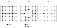
まず、マルチビームの全てのビームをオンにして、マルチビームで検査アパーチャ40をスキャンし、貫通孔42を通過する電子ビームを順次切り替え、各ビームのビーム電流検出結果を用いて、各ビームの位置を測定する(ステップS1)。例えば、図5(a)に示すように、マルチビームのうち、5×5のビームを測定領域とし、これらのビームで検査アパーチャ40をスキャンし、各ビームの位置を測定する。制御計算機110は、電流検出器50により検出されたビーム電流を輝度に変換し、主偏向器17の偏向量に基づいてビーム画像を作成し、ステージ位置検出器135により検出されたステージ位置から各ビームの位置を求める。
First, all the beams of the multi-beams are turned on, the
次に、測定領域の中心のビームをオフにした状態で検査アパーチャ40をスキャンし、貫通孔42を通過する電子ビームを順次切り替え、各ビームのビーム電流検出結果を用いて、各ビームの位置を測定する(ステップS2)。例えば、図5(b)に示すように、中心以外の24本のビームの位置を測定する。
Next, the
ビーム位置ずれ量算出部111が、ステップS1で測定したビーム位置と、ステップS2で測定したビーム位置との差分から、ビーム1本をオフにすることによる、周辺ビームの位置ずれ量を算出する(ステップS3)。そして、周辺ビームの位置ずれ量を定義した位置ずれマップを作成する(ステップS4)。例えば、図5(c)に示すような位置ずれマップが得られる。
The beam position
ステップS1~S4の処理を複数のフォーカスで実行する(ステップS5,S6)。これにより、複数のフォーカスの各々について、ビーム1本をオフにすることで周辺ビームがどのように位置ずれするかを示す位置ずれマップが作成される。作成された位置ずれマップは記憶装置142に格納される。この位置ずれマップは、焦点位置とマルチビームの各ビームの位置ずれ量との相関関係を示す。
The processing of steps S1 to S4 is executed with a plurality of focuses (steps S5 and S6). This creates a displacement map that shows how the peripheral beams are displaced by turning off one beam for each of the multiple focuses. The created positional deviation map is stored in the
次に、クーロン効果によるフォーカスずれとして、図6に示すフローチャートのように、マルチビームのビーム総電流量とフォーカス変動との関係を求める。 Next, as the defocus due to the Coulomb effect, the relationship between the total beam current amount of the multi-beam and the focus variation is obtained as shown in the flow chart of FIG.
まず、少なくとも一部のビームをオンにした状態でベストフォーカスを測定する(ステップS11)。例えば、マルチビームで検査アパーチャ40をスキャンし、貫通孔42を通過する電子ビームを順次切り替え、電流検出器50により検出されたビーム電流を輝度に変換し、ビーム画像を作成する。フォーカスを変えながらビーム画像を作成し、焦点位置算出部112が、各ビーム画像の輝度の分散からベストフォーカスを算出する。
First, the best focus is measured with at least part of the beams turned on (step S11). For example, the
オンビームの本数を変え、マルチビームのビーム総電流量毎にベストフォーカスを算出する(ステップS12,S13)。これにより、図7に示すようなビーム総電流量とベストフォーカスとなる焦点位置の変動量との関係が得られる。ビーム総電流量と焦点位置変動量との関係を示すフォーカス変動量情報は、記憶装置144に格納される。
By changing the number of on-beams, the best focus is calculated for each total beam current amount of the multi-beams (steps S12 and S13). As a result, the relationship between the total beam current amount and the amount of change in the focal position that provides the best focus is obtained as shown in FIG. Focus fluctuation amount information indicating the relationship between the total beam current amount and the focal position fluctuation amount is stored in the
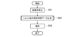
図8は、本実施形態に係る描画方法を説明するフローチャートである。面積率算出工程(ステップS21)として、面積率算出部113は、記憶装置140から描画データを読み出し、画素毎に、当該画素内のパターン面積密度(パターン面積率)を算出する。
FIG. 8 is a flowchart for explaining the drawing method according to this embodiment. As the area ratio calculation step (step S21), the area
ショット毎の照射時間データ生成工程(ステップS22)を図9に示すフローチャートを用いて詳細に説明する。 The shot-by-shot irradiation time data generation step (step S22) will be described in detail with reference to the flowchart shown in FIG.
照射量データ生成工程(ステップS201)では、照射量算出部114が、ショット毎に、マルチビームの各ビーム(個別ビーム)の照射量を算出する。例えば、照射量算出部114は、画素毎に、当該画素内のパターン面積密度と、予め設定された基準照射量とを乗じて照射量を算出する。近接効果補正係数をさらに乗じてもよい。
In the dose data generation step (step S201), the
フォーカス変動量算出工程(ステップS202)では、制御計算機110が、ショット毎に、マルチビームの全ビームの照射量を合計してビーム総電流量を求め、フォーカス変動量情報から、焦点位置の変動量を算出する。
In the focus variation calculation step (step S202), the
ビーム位置ずれ量算出工程(ステップS203)では、制御計算機110が、記憶装置142から、ステップS202で算出した焦点位置に対応する位置ずれマップを取り出す。制御計算機110は、オフビームの周辺のオンビームに、この位置ずれマップに定義された位置ずれ量を割り当て、各オンビームについて、割り当てられた位置ずれ量を重ね合わせて(加算して)、位置ずれ量を算出する。
In the beam position deviation amount calculation step (step S203), the
照射量変調工程(ステップS204)では、照射量変調部115が、ステップS203で算出された位置ずれを補正するため、ビーム毎に照射量を変調する。マルチビーム描画では、ビーム照射位置のずれを光学的に個別に補正することができないため、ビーム毎に照射量を変調し、位置ずれしたビームで露光した場合でも、レジストに与えるドーズ分布にビーム位置ずれの影響が現れないようにする。
In the dose modulation step (step S204), the
この照射量変調により、ビーム総電流量が変化する。制御計算機110は、照射量変調後のビーム総電流量を求め、フォーカス変動量情報から、焦点位置の変動量を算出する。判定部116は、焦点位置の変動量が所定値以下となるか判定する(ステップS205)。焦点位置の変動量が所定値以下となるまで、ビーム位置ずれ量算出工程(ステップS203)及び照射量変調工程(ステップS204)を繰り返し行う。
This dose modulation changes the total beam current. The
照射時間データ変換工程(ステップS206)では、描画制御部117が、変調後の各ビームの照射量を電流密度で除して照射時間データに変換し、偏向制御回路130へ転送する。
In the irradiation time data conversion step (step S206), the
描画工程(図8のステップS23)では、偏向制御回路130が、照射時間データに基づいて、ブランキングプレート10の各ブランカのオンオフを制御する。これにより、ビーム位置ずれの影響が現れないようにパターンを描画できる。
In the drawing process (step S23 in FIG. 8), the
このように、本実施形態によれば、ショット毎のビーム総電流量から焦点位置の変化量を算出し、変化した焦点位置におけるクロストークによるビーム位置ずれ量を算出する。そして、算出したビーム位置ずれ量を補正するように、各ビームの照射量を変調する。そのため、ビーム照射位置のずれを低減し、描画精度を向上させることができる。 As described above, according to the present embodiment, the amount of change in the focal position is calculated from the total beam current amount for each shot, and the amount of beam position deviation due to crosstalk at the focal position that has changed is calculated. Then, the irradiation amount of each beam is modulated so as to correct the calculated beam position deviation amount. Therefore, it is possible to reduce the deviation of the beam irradiation position and improve the writing accuracy.
上記実施形態では、焦点位置の変動量が所定値以下となるまで、ビーム位置ずれ量算出工程(ステップS203)及び照射量変調工程(ステップS204)を繰り返し行う例について説明したが、焦点位置の変動量からビーム位置ずれ量を算出し、ビーム位置ずれ量が所定値以下となるまで照射量変調工程(ステップS204)を繰り返し行ってもよい。 In the above embodiment, the beam position deviation calculation step (step S203) and the dose modulation step (step S204) are repeatedly performed until the amount of change in the focal position becomes equal to or less than a predetermined value. A beam position deviation amount may be calculated from the amount, and the dose modulation step (step S204) may be repeated until the beam position deviation amount becomes equal to or less than a predetermined value.
上記実施形態では、クロストークに起因する出射角異常によるビーム位置ずれを考慮する例について説明したが、出射角異常はブランキングプレート10の製作精度不良によっても生じ得る。 In the above embodiment, an example has been described in which beam position deviation due to an output angle anomaly due to crosstalk is taken into account.
ブランキングプレート10の製作精度不良に起因する出射角異常によるビーム位置ずれを考慮する場合は、各ビームの出射角異常を考慮する必要はなく、ある程度のビームのまとまり毎に出射角を考慮すればよい。
When taking into consideration the beam position deviation due to the output angle abnormality caused by the manufacturing inaccuracy of the blanking
例えば、図10に示すように、32×32のビームを1ブロック(1グループ)とし、512×512のビームからなるビームアレイ(マルチビーム)を256個のブロックに分割する。 For example, as shown in FIG. 10, 32×32 beams are defined as one block (one group), and a beam array (multi-beam) consisting of 512×512 beams is divided into 256 blocks.
ブランキングプレート10の製作精度不良に起因する出射角異常によるビーム位置ずれの算出方法を図11に沿って説明する。まず、1つのブロックのビームを全てオンにして検査アパーチャ40をスキャンし、各ビームの位置を測定する(ステップS31)。測定した位置と、理想位置のずれから、ビーム位置ずれ量を算出する(ステップS32)。ここで算出するビーム位置ずれ量は、例えば、32×32本のビームの位置ずれ量の平均値などの代表値である。
A method of calculating the beam position deviation due to the output angle abnormality caused by the manufacturing inaccuracy of the blanking
ステップS31、S32の処理を複数のフォーカスで実行する(ステップS33,S34)。複数のフォーカスの各々について、ビーム位置ずれ量の代表値を求めたら、別のブロックで同様の処理を行う(ステップS31~S36)。全てのブロックについてこれらの処理を行い、フォーカス毎の位置ずれマップを作成し、記憶装置142に格納する(ステップS37)。 The processes of steps S31 and S32 are executed with a plurality of focuses (steps S33 and S34). After obtaining the representative value of the beam position deviation amount for each of the plurality of focuses, similar processing is performed in another block (steps S31 to S36). These processes are performed for all blocks, a position shift map for each focus is created, and stored in the storage device 142 (step S37).
図9のビーム位置ずれ量算出工程(ステップS203)では、この位置ずれマップを用いて、各ブロックの出射角異常によって引き起こされる各ビームの位置ずれ量を算出する。 In the beam position deviation amount calculation step (step S203) in FIG. 9, the position deviation amount of each beam caused by the emission angle abnormality of each block is calculated using this position deviation map.
なお、本発明は上記実施形態そのままに限定されるものではなく、実施段階ではその要旨を逸脱しない範囲で構成要素を変形して具体化できる。また、上記実施形態に開示されている複数の構成要素の適宜な組み合わせにより、種々の発明を形成できる。例えば、実施形態に示される全構成要素から幾つかの構成要素を削除してもよい。さらに、異なる実施形態にわたる構成要素を適宜組み合わせてもよい。 It should be noted that the present invention is not limited to the above-described embodiments as they are, and can be embodied by modifying constituent elements without departing from the scope of the present invention at the implementation stage. Further, various inventions can be formed by appropriate combinations of the plurality of constituent elements disclosed in the above embodiments. For example, some components may be omitted from all components shown in the embodiments. Furthermore, components across different embodiments may be combined as appropriate.
1 描画部
2 電子鏡筒
4 電子銃
6 照明レンズ
8 成形アパーチャアレイ基板
10 ブランキングプレート
12 縮小レンズ
14 制限アパーチャ部材
15 対物レンズ
16 コイル
17 主偏向器
20 描画室
22 XYステージ
40 検査アパーチャ
50 電流検出器
100 制御部
110 制御計算機
1 Drawing
Claims (5)
成形アパーチャアレイ基板に設けられた複数の開口を前記荷電粒子ビームが通過することによりマルチビームを形成する工程と、
前記マルチビームの各ビームに対応するブランカが設けられたブランキングプレートを用いて、各ビームのオンオフを切り替える工程と、
前記マルチビームの焦点位置の変動量を算出する工程と、
予め求められた焦点位置と前記マルチビームの各ビームの位置ずれ量との相関関係に基づき、算出された前記焦点位置より前記位置ずれ量を算出する工程と、
前記位置ずれ量に基づいて、前記マルチビームの各ビームの照射量を変調する工程と、
変調後の照射量で前記マルチビームを基板に照射してパターンを描画する工程と、
を備えるマルチ荷電粒子ビーム描画方法。 emitting a charged particle beam;
forming multiple beams by passing the charged particle beams through a plurality of apertures provided in a shaped aperture array substrate;
a step of switching on and off each beam using a blanking plate provided with a blanker corresponding to each beam of the multi-beam;
a step of calculating a variation amount of the focal position of the multi-beam;
a step of calculating the amount of positional deviation from the calculated focal position based on the correlation between the focal position obtained in advance and the amount of positional deviation of each beam of the multi-beam;
modulating the irradiation amount of each beam of the multi-beam based on the amount of positional deviation;
a step of irradiating the substrate with the multi-beam at the modulated dose to draw a pattern;
A multi-charged particle beam writing method comprising:
複数の開口が形成され、前記複数の開口を前記荷電粒子ビームが通過することによりマルチビームを形成する成形アパーチャアレイ基板と、
前記マルチビームの各ビームにそれぞれ対応し、ビームのオンオフを切り替える複数のブランカが配置されたブランキングプレートと、
前記マルチビームの焦点位置の変動量を算出し、予め求められた焦点位置と前記マルチビームの各ビームの位置ずれ量との相関関係に基づき、算出された前記焦点位置より前記位置ずれ量を算出し、前記位置ずれ量に基づいて、各ビームの照射量を変調する制御計算機と、
変調後の照射量に基づいて前記複数のブランカを制御する偏向制御回路と、
を備えるマルチ荷電粒子ビーム描画装置。 an emitter for emitting a charged particle beam;
a shaped aperture array substrate in which a plurality of apertures are formed and the charged particle beams pass through the plurality of apertures to form a multi-beam;
a blanking plate on which a plurality of blankers corresponding to each beam of the multi-beam and for switching the beams on and off are arranged;
calculating the amount of change in the focal position of the multi-beam, and calculating the amount of positional deviation from the calculated focal position based on the correlation between the focal position obtained in advance and the amount of positional deviation of each beam of the multi-beam; and a control computer that modulates the irradiation amount of each beam based on the positional deviation amount;
a deflection control circuit that controls the plurality of blankers based on the modulated dose;
A multi-charged particle beam lithography system.
Priority Applications (1)
| Application Number | Priority Date | Filing Date | Title |
|---|---|---|---|
| JP2019111319A JP7176480B2 (en) | 2019-06-14 | 2019-06-14 | Multi-charged particle beam writing method and multi-charged particle beam writing apparatus |
Applications Claiming Priority (1)
| Application Number | Priority Date | Filing Date | Title |
|---|---|---|---|
| JP2019111319A JP7176480B2 (en) | 2019-06-14 | 2019-06-14 | Multi-charged particle beam writing method and multi-charged particle beam writing apparatus |
Publications (2)
| Publication Number | Publication Date |
|---|---|
| JP2020205314A JP2020205314A (en) | 2020-12-24 |
| JP7176480B2 true JP7176480B2 (en) | 2022-11-22 |
Family
ID=73837515
Family Applications (1)
| Application Number | Title | Priority Date | Filing Date |
|---|---|---|---|
| JP2019111319A Active JP7176480B2 (en) | 2019-06-14 | 2019-06-14 | Multi-charged particle beam writing method and multi-charged particle beam writing apparatus |
Country Status (1)
| Country | Link |
|---|---|
| JP (1) | JP7176480B2 (en) |
Citations (6)
| Publication number | Priority date | Publication date | Assignee | Title |
|---|---|---|---|---|
| JP2015216225A (en) | 2014-05-09 | 2015-12-03 | キヤノン株式会社 | Lithography apparatus and method, and method of manufacturing article |
| JP2016103557A (en) | 2014-11-28 | 2016-06-02 | 株式会社ニューフレアテクノロジー | Multiple charged particle beam lithography apparatus and multiple charged particle beam lithography method |
| JP2016119423A (en) | 2014-12-22 | 2016-06-30 | 株式会社ニューフレアテクノロジー | Multiple charged particle beam lithography apparatus and multiple charged particle beam lithography method |
| JP2018078251A (en) | 2016-11-11 | 2018-05-17 | 株式会社ニューフレアテクノロジー | Multi-charged particle beam lithography device |
| JP2018182189A (en) | 2017-04-19 | 2018-11-15 | 株式会社ニューフレアテクノロジー | Multi-charged particle beam lithography device and multi-charged particle beam lithography method |
| US20190164721A1 (en) | 2017-11-29 | 2019-05-30 | Hermes Microvision, Inc. | Systems and methods for charged particle beam modulation |
-
2019
- 2019-06-14 JP JP2019111319A patent/JP7176480B2/en active Active
Patent Citations (6)
| Publication number | Priority date | Publication date | Assignee | Title |
|---|---|---|---|---|
| JP2015216225A (en) | 2014-05-09 | 2015-12-03 | キヤノン株式会社 | Lithography apparatus and method, and method of manufacturing article |
| JP2016103557A (en) | 2014-11-28 | 2016-06-02 | 株式会社ニューフレアテクノロジー | Multiple charged particle beam lithography apparatus and multiple charged particle beam lithography method |
| JP2016119423A (en) | 2014-12-22 | 2016-06-30 | 株式会社ニューフレアテクノロジー | Multiple charged particle beam lithography apparatus and multiple charged particle beam lithography method |
| JP2018078251A (en) | 2016-11-11 | 2018-05-17 | 株式会社ニューフレアテクノロジー | Multi-charged particle beam lithography device |
| JP2018182189A (en) | 2017-04-19 | 2018-11-15 | 株式会社ニューフレアテクノロジー | Multi-charged particle beam lithography device and multi-charged particle beam lithography method |
| US20190164721A1 (en) | 2017-11-29 | 2019-05-30 | Hermes Microvision, Inc. | Systems and methods for charged particle beam modulation |
Also Published As
| Publication number | Publication date |
|---|---|
| JP2020205314A (en) | 2020-12-24 |
Similar Documents
| Publication | Publication Date | Title |
|---|---|---|
| US7521700B2 (en) | Raster frame beam system for electron beam lithography | |
| US11037759B2 (en) | Multi charged particle beam writing apparatus and multi charged particle beam writing method | |
| US10483088B2 (en) | Multi charged particle beam writing apparatus and multi charged particle beam writing method | |
| KR101843056B1 (en) | Charged particle beam writing apparatus and charged particle beam writing method | |
| JP7180515B2 (en) | Multi-charged particle beam writing apparatus and multi-charged particle beam writing method | |
| US10867774B2 (en) | Multi charged particle beam writing apparatus and multi charged particle beam writing method | |
| JP2017220615A (en) | Multi-charged-particle-beam exposure apparatus and adjustment method therefor | |
| TW202001968A (en) | Data processing method, data processing apparatus, and multiple charged-particle beam writing apparatus | |
| JP7400830B2 (en) | Multi-charged particle beam adjustment method, multi-charged particle beam irradiation method, and multi-charged particle beam irradiation device | |
| JP2022146501A (en) | Multi-charged particle beam lithography apparatus and adjustment method for the same | |
| US10636616B2 (en) | Aperture array alignment method and multi charged particle beam writing apparatus | |
| US10283314B2 (en) | Charged particle beam writing apparatus, and charged particle beam writing method | |
| JP7176480B2 (en) | Multi-charged particle beam writing method and multi-charged particle beam writing apparatus | |
| JP7196792B2 (en) | Multi-beam writing method and multi-beam writing apparatus | |
| JP7238672B2 (en) | Multi-beam writing method and multi-beam writing apparatus | |
| US20220359156A1 (en) | Multi charged particle beam writing method and multi charged particle beam writing apparatus | |
| KR20210012951A (en) | Multi-beam writing method and multi-beam writing apparatus |
Legal Events
| Date | Code | Title | Description |
|---|---|---|---|
| A621 | Written request for application examination |
Free format text: JAPANESE INTERMEDIATE CODE: A621 Effective date: 20220204 |
|
| A977 | Report on retrieval |
Free format text: JAPANESE INTERMEDIATE CODE: A971007 Effective date: 20220928 |
|
| TRDD | Decision of grant or rejection written | ||
| A01 | Written decision to grant a patent or to grant a registration (utility model) |
Free format text: JAPANESE INTERMEDIATE CODE: A01 Effective date: 20221011 |
|
| A61 | First payment of annual fees (during grant procedure) |
Free format text: JAPANESE INTERMEDIATE CODE: A61 Effective date: 20221024 |
|
| R150 | Certificate of patent or registration of utility model |
Ref document number: 7176480 Country of ref document: JP Free format text: JAPANESE INTERMEDIATE CODE: R150 |