KR20140130029A - Drawing apparatus, and method of manufacturing article - Google Patents
Drawing apparatus, and method of manufacturing article Download PDFInfo
- Publication number
- KR20140130029A KR20140130029A KR20140047894A KR20140047894A KR20140130029A KR 20140130029 A KR20140130029 A KR 20140130029A KR 20140047894 A KR20140047894 A KR 20140047894A KR 20140047894 A KR20140047894 A KR 20140047894A KR 20140130029 A KR20140130029 A KR 20140130029A
- Authority
- KR
- South Korea
- Prior art keywords
- charged particle
- substrate
- region
- area
- optical system
- Prior art date
Links
Images
Classifications
-
- H—ELECTRICITY
- H01—ELECTRIC ELEMENTS
- H01J—ELECTRIC DISCHARGE TUBES OR DISCHARGE LAMPS
- H01J37/00—Discharge tubes with provision for introducing objects or material to be exposed to the discharge, e.g. for the purpose of examination or processing thereof
- H01J37/02—Details
- H01J37/04—Arrangements of electrodes and associated parts for generating or controlling the discharge, e.g. electron-optical arrangement, ion-optical arrangement
- H01J37/045—Beam blanking or chopping, i.e. arrangements for momentarily interrupting exposure to the discharge
-
- H—ELECTRICITY
- H01—ELECTRIC ELEMENTS
- H01J—ELECTRIC DISCHARGE TUBES OR DISCHARGE LAMPS
- H01J37/00—Discharge tubes with provision for introducing objects or material to be exposed to the discharge, e.g. for the purpose of examination or processing thereof
- H01J37/02—Details
- H01J37/20—Means for supporting or positioning the objects or the material; Means for adjusting diaphragms or lenses associated with the support
-
- H—ELECTRICITY
- H01—ELECTRIC ELEMENTS
- H01J—ELECTRIC DISCHARGE TUBES OR DISCHARGE LAMPS
- H01J37/00—Discharge tubes with provision for introducing objects or material to be exposed to the discharge, e.g. for the purpose of examination or processing thereof
- H01J37/30—Electron-beam or ion-beam tubes for localised treatment of objects
- H01J37/317—Electron-beam or ion-beam tubes for localised treatment of objects for changing properties of the objects or for applying thin layers thereon, e.g. for ion implantation
- H01J37/3174—Particle-beam lithography, e.g. electron beam lithography
- H01J37/3177—Multi-beam, e.g. fly's eye, comb probe
-
- H—ELECTRICITY
- H01—ELECTRIC ELEMENTS
- H01L—SEMICONDUCTOR DEVICES NOT COVERED BY CLASS H10
- H01L21/00—Processes or apparatus adapted for the manufacture or treatment of semiconductor or solid state devices or of parts thereof
- H01L21/02—Manufacture or treatment of semiconductor devices or of parts thereof
- H01L21/027—Making masks on semiconductor bodies for further photolithographic processing not provided for in group H01L21/18 or H01L21/34
- H01L21/0271—Making masks on semiconductor bodies for further photolithographic processing not provided for in group H01L21/18 or H01L21/34 comprising organic layers
- H01L21/0273—Making masks on semiconductor bodies for further photolithographic processing not provided for in group H01L21/18 or H01L21/34 comprising organic layers characterised by the treatment of photoresist layers
- H01L21/0274—Photolithographic processes
-
- H—ELECTRICITY
- H01—ELECTRIC ELEMENTS
- H01J—ELECTRIC DISCHARGE TUBES OR DISCHARGE LAMPS
- H01J2237/00—Discharge tubes exposing object to beam, e.g. for analysis treatment, etching, imaging
- H01J2237/30—Electron or ion beam tubes for processing objects
- H01J2237/317—Processing objects on a microscale
- H01J2237/3175—Lithography
- H01J2237/31761—Patterning strategy
Abstract
Description
The present invention relates to a drawing apparatus and a method of manufacturing an article.
An imaging apparatus using charged particle beams such as electron beams performs overlay imaging that draws a new pattern superimposed on a pattern (hereinafter referred to as a "shot pattern") formed in each shot region of the substrate.
In the overlay drawing, first, the substrate is moved based on the array coordinate values in the design of the plurality of shot patterns, and a position when a part of the plurality of shot patterns is aligned with the reference position is actually measured. Next, assuming that the array coordinate values in the design of the shot pattern and the actual array coordinate values to be aligned are in a specific relationship including a predetermined error, the average value An error parameter is determined such that the deviation is minimized. Based on the error parameter and the array coordinate values in the design of the shot pattern, the actual array coordinate values of the shot pattern are obtained. The substrate is positioned according to the actual array coordinate value, and the pattern is drawn.
In such overlay drawing, distortion (e.g., stretching / shrinking and rotation) of the shot pattern is measured along with the actual array coordinate value of the shot pattern. The distortion of the shot pattern is caused by a factor of a lithographic apparatus such as a drawing apparatus at the time of forming a pattern or by a deformation of a substrate due to a heat treatment at the time of forming a pattern.
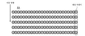
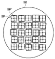
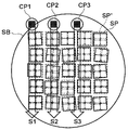
5A is a diagram showing an array of 5 (rows) x 5 (rows) shot patterns formed on the substrate SB. The actual shot pattern SP is indicated by a solid line, and the shot pattern SP 'in design is indicated by a dashed line. FIG. 5B shows a state in which overlay imaging is performed by the imaging apparatus including the plurality of charged particle optical systems CP1, CP2, and CP3 with respect to the substrate SB (actual shot pattern SP). Referring to Fig. 5B, each of the charged particle optics CP1 to CP3 emits 5 (rows) x 5 (rows) of charged particle beams to the substrate SB. When the stage holding the substrate SB is moved upward with respect to the charged particle optical systems CP1, CP2, and CP3, the charged particle optical systems CP1, CP2, and CP3 respectively draw stripe regions S1, S2, and S3 (stripe drawing). In such stripe drawing, multiple irradiation is performed on the same position of the substrate by the charged particle beam arranged in the substrate moving direction of the charged particle optical system. Such irradiation is on / off controlled to control the dose of the charged particle beam on the substrate.
Each charged particle optical system includes a deflector configured to deflect a charged particle beam. These deflectors collectively adjust the positions of the plurality of charged particle beams (the imaging areas defined by the substrate). In the stripe drawing, a new pattern is superimposed on the shot pattern while drawing the area of the drawing region of the charged particle optical system by the deflector based on the actual position of the shot pattern on the substrate.
However, depending on the dimensions of the shot pattern, as in the charged particle optical system CP3 shown in Fig. 5B, the imaging area of the charged particle optical system is vibrated over the shot pattern adjacent in the direction orthogonal to the substrate moving direction Lt; RTI ID = 0.0 > and / or < / RTI > This poses the following problems. In fact, the shot patterns on the substrate are not always regularly arranged along the array coordinates in the design (i.e., the positions of the shot patterns are shifted). Therefore, it is necessary to perform drawing while adjusting (correcting) the position of the drawing area with respect to the shot pattern. However, when the imaging area of the charged particle optical system spans a shot pattern adjacent in the direction orthogonal to the substrate moving direction, the position of the imaging area of the charged particle optical system can be corrected for only one of the shot patterns.
In order to solve such a problem, Japanese Patent Application Laid-Open No. 2004-172428 proposes an imaging apparatus capable of mechanically adjusting the distance between optical axes of a plurality of charged particle optical systems.
However, in this conventional technique, there is not sufficient precision in mechanically adjusting the distance between the optical axes of the plurality of charged particle optical systems, and the overlay accuracy required in recent overlay imaging can not be satisfied.
The present invention provides an imaging apparatus advantageous from the viewpoint of overlay accuracy, for example, when imaging is performed on a substrate using a plurality of charged particle optical systems.
According to an aspect of the present invention, there is provided an imaging apparatus for imaging a charged particle beam on a substrate, the imaging apparatus having a blanking function for individually blanking a plurality of charged particle beams arranged in a first direction, A plurality of charged particle optical systems disposed on the stage, a stage configured to hold and move the substrate, and a control unit configured to control the imaging operation performed by the movement of the stage and the respective blanking functions of the plurality of charged particle optical systems Wherein the plurality of charged particle beams among the plurality of charged particle optical systems reach a first region and a second region adjacent to each other in the first direction formed on the substrate The first charged particle optical system is moved in the second direction while moving the stage, Wherein the control unit is configured to perform the control so that only one of the plurality of charged particle beams performs imaging with the charged particle beam of the first one of the plurality of charged particle beams.
Further aspects of the present invention will become apparent from the following description of exemplary embodiments with reference to the accompanying drawings.
BRIEF DESCRIPTION OF THE DRAWINGS Fig. 1 is a schematic view showing a configuration of a drawing apparatus according to an embodiment of the present invention; Fig.
Fig. 2 is a schematic view showing a configuration of a charged particle optical system of the imaging apparatus shown in Fig. 1; Fig.
Figs. 3A to 3C are diagrams for explaining the drawing process of the drawing apparatus shown in Fig. 1; Fig.
Figs. 4A to 4C are diagrams for describing the drawing process of the drawing apparatus shown in Fig. 1; Fig.
5A and 5B are diagrams for explaining stripe drawing in overlay drawing.
Hereinafter, preferred embodiments of the present invention will be described with reference to the accompanying drawings. In the drawings, the same reference numerals denote the same members, and a repeated description thereof will be omitted.
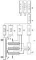
1 is a schematic diagram showing the configuration of a
The
Each of the first charged particle
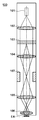
2 is a schematic diagram showing the configuration of a charged particle
The
The
The
Referring again to FIG. 1, the
The position detection system (detection unit) 12 includes an irradiation system configured to irradiate a mark (for example, an alignment mark) formed on the
The blanking
The
The
The
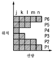
Figs. 3A to 3C are diagrams for explaining the drawing process of the
In this case, the
In this case, on / off per unit clock of each charged particle line of each row j to n of the target charged particle array (i.e., whether or not the charged particle beam is irradiated to the substrate) When set (controlled), the relationship shown in FIG. 3B is obtained. Referring to FIG. 3C, the dotted line corresponds to a signal indicating the on (square) and off (no symbol) of the charged particle lines of rows j through n that illuminate positions P1 through P6 on the substrate. This is because the
4A to 4C, a plurality of shot regions SH of the substrate are formed by using the first charged particle
4A, EA1 represents an imaging area defined by a charged particle beam emitted by the first charged particle
4A, the painting areas EA1, EA2, and EA3 do not overlap two shot areas adjacent in the direction perpendicular to the moving direction of the
In Fig. 4B, the painting areas EA1 and EA2 are not spanned over two shot areas adjacent in the direction perpendicular to the moving direction of the
In FIG. 4C, since the drawing by the drawing areas EA1 and EA2 is completed (FIG. 4B), the drawing is not performed in the drawing areas EA1 and EA2 (that is, drawing in the drawing areas EA1 and EA2 is prohibited). On the other hand, for the drawing area EA3, the overlay drawing is performed on a part of the drawing area EA3, that is, the second shot area SH2 of the second drawing area EA3b, and the drawing is not performed in the first drawing area EA3a Rendering in EA3a is prohibited). In other words, only one of the first shot area SH1 and the second shot area SH2 is drawn. More specifically, while the
As described above, the
In this embodiment, for the first charged particle
In the present embodiment, rendering of one shot area on the substrate has been described in units. However, the drawing unit of the
Since the
While the present invention has been described with reference to exemplary embodiments, it is to be understood that the invention is not limited to the disclosed exemplary embodiments. The scope of the following claims is to be accorded the broadest interpretation so as to encompass all such modifications and equivalent structures and functions.
Claims (10)
A plurality of charged particle optical systems each having a blanking function for separately blanking a plurality of charged particle beams arranged in a first direction and arranged at intervals in the first direction,
A stage configured to hold and move the substrate,
And a controller configured to perform control of drawing performed by the movement of the stage and the blanking function of each of the plurality of charged particle optical systems,
Wherein the controller controls the first charged particle optical system in which the plurality of charged particle beams of the plurality of charged particle optical systems reach a first region and a second region adjacent to each other in the first direction formed on the substrate, While the stage is moved in the second direction so that drawing is performed on the charged particle beam of the first portion of the plurality of charged particle beams only in one of the first region and the second region.
Wherein the controller is configured to control, during drawing of one of the first area and the second area, based on information of a target drawing position relating to one of the first area and the second area, The charged particle beam is deflected and, during imaging of the other of the first region and the second region, by the deflector based on information of the object imaging position about the other of the first region and the second region And control is performed so that the charged particle beam of the second portion is deflected.
Wherein the controller is configured to obtain information on the target drawing position for each of one and the other of the first area and the second area based on an output of the detector.
A method of manufacturing a semiconductor device, comprising the steps of: drawing a substrate using the imaging apparatus according to any one of claims 1 to 9;
Developing the substrate on which imaging is performed;
And processing the developed substrate to produce the article.
Applications Claiming Priority (2)
| Application Number | Priority Date | Filing Date | Title |
|---|---|---|---|
| JP2013095961A JP2014216631A (en) | 2013-04-30 | 2013-04-30 | Drawing apparatus, and method of manufacturing article |
| JPJP-P-2013-095961 | 2013-04-30 |
Publications (1)
| Publication Number | Publication Date |
|---|---|
| KR20140130029A true KR20140130029A (en) | 2014-11-07 |
Family
ID=51788475
Family Applications (1)
| Application Number | Title | Priority Date | Filing Date |
|---|---|---|---|
| KR20140047894A KR20140130029A (en) | 2013-04-30 | 2014-04-22 | Drawing apparatus, and method of manufacturing article |
Country Status (5)
| Country | Link |
|---|---|
| US (1) | US9293292B2 (en) |
| JP (1) | JP2014216631A (en) |
| KR (1) | KR20140130029A (en) |
| CN (1) | CN104134603A (en) |
| TW (1) | TWI556063B (en) |
Families Citing this family (4)
| Publication number | Priority date | Publication date | Assignee | Title |
|---|---|---|---|---|
| JP6195349B2 (en) * | 2013-04-26 | 2017-09-13 | キヤノン株式会社 | Drawing apparatus, drawing method, and article manufacturing method |
| JP2016092136A (en) * | 2014-10-31 | 2016-05-23 | キヤノン株式会社 | Drawing device, and method of manufacturing article |
| JP6616986B2 (en) * | 2015-09-14 | 2019-12-04 | 株式会社ニューフレアテクノロジー | Multi-charged particle beam writing method and multi-charged particle beam writing apparatus |
| JP2019102661A (en) * | 2017-12-04 | 2019-06-24 | 株式会社ニューフレアテクノロジー | Acquisition method of beam deflection shape and acquisition method of arrangement angle of blanking aperture array |
Family Cites Families (8)
| Publication number | Priority date | Publication date | Assignee | Title |
|---|---|---|---|---|
| JP3647128B2 (en) * | 1996-03-04 | 2005-05-11 | キヤノン株式会社 | Electron beam exposure apparatus and exposure method thereof |
| JPH1092356A (en) * | 1996-09-19 | 1998-04-10 | Seiko Instr Inc | Optical axis control method for focused ion beam and focused ion beam device |
| JP4308504B2 (en) | 2002-11-21 | 2009-08-05 | 株式会社荏原製作所 | Electron beam apparatus and device manufacturing method using the apparatus |
| TWI602033B (en) * | 2007-12-28 | 2017-10-11 | Nippon Kogaku Kk | Exposure apparatus, moving body driving system, pattern forming apparatus, exposure method, and device manufacturing method |
| CN103069536B (en) * | 2010-04-09 | 2016-04-06 | 卡尔蔡司Smt有限责任公司 | Charged particle detection system and m ultiwavelet bundle check system |
| TWI534852B (en) * | 2010-10-26 | 2016-05-21 | 瑪波微影Ip公司 | Lithography system, modulation device and method of manufacturing a fiber fixation substrate |
| JP2013045838A (en) * | 2011-08-23 | 2013-03-04 | Canon Inc | Drawing device and manufacturing method of article |
| JP2013178961A (en) * | 2012-02-28 | 2013-09-09 | Canon Inc | Charged particle beam device and article manufacturing method |
-
2013
- 2013-04-30 JP JP2013095961A patent/JP2014216631A/en not_active Withdrawn
-
2014
- 2014-03-21 TW TW103110670A patent/TWI556063B/en active
- 2014-03-28 US US14/228,415 patent/US9293292B2/en not_active Expired - Fee Related
- 2014-04-22 KR KR20140047894A patent/KR20140130029A/en active IP Right Grant
- 2014-04-25 CN CN201410169271.XA patent/CN104134603A/en active Pending
Also Published As
| Publication number | Publication date |
|---|---|
| US9293292B2 (en) | 2016-03-22 |
| TW201441771A (en) | 2014-11-01 |
| TWI556063B (en) | 2016-11-01 |
| CN104134603A (en) | 2014-11-05 |
| US20140319367A1 (en) | 2014-10-30 |
| JP2014216631A (en) | 2014-11-17 |
Similar Documents
| Publication | Publication Date | Title |
|---|---|---|
| US9236224B2 (en) | Drawing apparatus and method of manufacturing article | |
| JP5505821B2 (en) | Pattern lock device for particle beam exposure apparatus | |
| JP5835892B2 (en) | Charged particle beam drawing apparatus and device manufacturing method | |
| US8759797B2 (en) | Drawing apparatus, drawing method, and method of manufacturing article | |
| KR101721070B1 (en) | Drawing apparatus, and method of manufacturing article | |
| KR101790829B1 (en) | Drawing apparatus, and method of manufacturing article | |
| KR20140130029A (en) | Drawing apparatus, and method of manufacturing article | |
| US20150131075A1 (en) | Drawing apparatus, and method of manufacturing article | |
| US9558916B2 (en) | Lithography system and method of manufacturing articles | |
| KR20150018397A (en) | Drawing data generating method, processing apparatus, storage medium, drawing apparatus, and method of manufacturing article | |
| US20150129779A1 (en) | Drawing apparatus, and method of manufacturing article | |
| US20160126061A1 (en) | Drawing apparatus and device manufacturing method | |
| JP2015037104A (en) | Drawing apparatus and manufacturing method for article | |
| US20150187540A1 (en) | Drawing apparatus and method of manufacturing article | |
| JP2016115811A (en) | Drawing apparatus, and manufacturing method for article | |
| JP2005183540A (en) | Method of exposure and mask | |
| JP2016086101A (en) | Lithographic apparatus and manufacturing method of article |
Legal Events
| Date | Code | Title | Description |
|---|---|---|---|
| A201 | Request for examination | ||
| E902 | Notification of reason for refusal | ||
| E701 | Decision to grant or registration of patent right |