JP6233872B2 - LED manufacturing method - Google Patents
LED manufacturing method Download PDFInfo
- Publication number
- JP6233872B2 JP6233872B2 JP2013050950A JP2013050950A JP6233872B2 JP 6233872 B2 JP6233872 B2 JP 6233872B2 JP 2013050950 A JP2013050950 A JP 2013050950A JP 2013050950 A JP2013050950 A JP 2013050950A JP 6233872 B2 JP6233872 B2 JP 6233872B2
- Authority
- JP
- Japan
- Prior art keywords
- slurry
- led
- phosphor
- binder
- manufacturing
- Prior art date
- Legal status (The legal status is an assumption and is not a legal conclusion. Google has not performed a legal analysis and makes no representation as to the accuracy of the status listed.)
- Active
Links
Images


Classifications
-
- H—ELECTRICITY
- H01—ELECTRIC ELEMENTS
- H01L—SEMICONDUCTOR DEVICES NOT COVERED BY CLASS H10
- H01L2224/00—Indexing scheme for arrangements for connecting or disconnecting semiconductor or solid-state bodies and methods related thereto as covered by H01L24/00
- H01L2224/01—Means for bonding being attached to, or being formed on, the surface to be connected, e.g. chip-to-package, die-attach, "first-level" interconnects; Manufacturing methods related thereto
- H01L2224/42—Wire connectors; Manufacturing methods related thereto
- H01L2224/47—Structure, shape, material or disposition of the wire connectors after the connecting process
- H01L2224/48—Structure, shape, material or disposition of the wire connectors after the connecting process of an individual wire connector
- H01L2224/4805—Shape
- H01L2224/4809—Loop shape
- H01L2224/48091—Arched
-
- H—ELECTRICITY
- H01—ELECTRIC ELEMENTS
- H01L—SEMICONDUCTOR DEVICES NOT COVERED BY CLASS H10
- H01L2224/00—Indexing scheme for arrangements for connecting or disconnecting semiconductor or solid-state bodies and methods related thereto as covered by H01L24/00
- H01L2224/80—Methods for connecting semiconductor or other solid state bodies using means for bonding being attached to, or being formed on, the surface to be connected
- H01L2224/85—Methods for connecting semiconductor or other solid state bodies using means for bonding being attached to, or being formed on, the surface to be connected using a wire connector
- H01L2224/85909—Post-treatment of the connector or wire bonding area
- H01L2224/8592—Applying permanent coating, e.g. protective coating
Description
本発明はLEDに蛍光体を施与してLEDを製造する方法に関する。
特に、本発明は樹脂、溶液、蛍光体を含むスラーリーなどをLEDに充填または塗布し乾燥硬化する方法に係わり、さらには白色発光LEDを製造するための方法に係わる。尚、本明細書中LED用部材とは完成品としてのLEDを製造する途中の中間部品としての部材等を意味しており、また本発明の塗布とは、連続的又は断続的なディスペンス、インクジェット、マイクロカーテン施与、スロットノズル施与、スクリーンプリンティング方式、霧化施与、スプレイ等を含むがこれらに限定するものではない。
The present invention relates to a method of manufacturing an LED by applying a phosphor to the LED.
In particular, the present invention relates to a method of filling or applying a resin, a solution, a slurry containing phosphor and the like to an LED and then drying and curing, and further relates to a method for manufacturing a white light emitting LED. In the present specification, the LED member means a member or the like as an intermediate part in the process of manufacturing an LED as a finished product, and the application of the present invention means continuous or intermittent dispensing or inkjet. , Micro curtain application, slot nozzle application, screen printing method, atomization application, spraying and the like.
従来、白色発光LEDの製造方法として紫外光や青色発光ダイオードにRGBや少なくとも一つのYAG、TAG,シリカ(silica)系などの蛍光体と2液反応熱硬化タイプシリコーンなどのバインダーを混合したスラーリー(slurry)をディスペンサー装置でディスペンス(dispense)したり、更に溶剤などを加えて粘度を低くし微粒子発生装置の一種であるスプレイ装置などを用いてLEDに直接スプレイ(spray)し被覆していた。 Conventionally, as a method for producing a white light emitting LED, an ultraviolet light or a blue light emitting diode is mixed with a phosphor such as RGB, at least one YAG, TAG, silica (silica) and a binder such as a two-component reaction thermosetting type silicone ( The slurry was dispensed with a dispenser device, or a solvent was added to lower the viscosity, and the LED was directly sprayed on the LED using a spray device, which is a kind of fine particle generator, and coated.
特許文献1は本出願人により加熱したLEDチップ(chip)に蛍光体(phosphor)とバインダーと溶媒を含むスラーリーを圧縮エア(air)を用いて薄膜で多層にスプレイ塗布し、一般的なスプレイ方法ではコーティング(coating)することが難しいとされるLEDの側壁にも付着させてLEDを製造する方法が提案されている。 Patent Document 1 discloses a general spraying method in which a slurry containing phosphor, a binder and a solvent is applied to an LED chip heated by the present applicant in a thin film using a compressed air. Then, a method of manufacturing an LED by adhering to the side wall of the LED which is difficult to coat has been proposed.
特許文献2にはLEDチップにシリコーン(silicon)などのバインダー(binder)を被覆し硬化させて、その上に蛍光体、バインダー、溶剤からなるスラーリー(slurry)を塗布し、必要により拡散材などをそれらに混合して積層する方法が提案されている。
In
非特許文献1などに開示されているようなディスペンサー(dispenser)を用いる方法はハイパワー(high power)でない砲弾型LEDやバックライト(back light)向けなどのカップ(cup)の内側に装着されたチップに前記スラーリーを充填して大量生産向けに多く採用されている。 A method using a dispenser as disclosed in Non-Patent Document 1 is mounted inside a cup such as a bullet-type LED that is not high power or a backlight (back light). Many of these chips are used for mass production by filling the slurry.
しかし、特許文献1の方法ではパルス的にスラーリーを塗布できるのでLEDチップの側壁もコーティングでき、また薄膜で多層に塗布するのでLEDチップのエッジカバーもよく、塗着効率も極めて高くできるが、セラミックスなどのLED基板に組み込まれたLEDとLEDの間まで塗布するか、不必要な個所はマスクをして塗布するので蛍光体の使用効率は低かった。特にLED間の距離が離れている場合は極めて効率が悪かった。 However, in the method of Patent Document 1, the slurry can be applied in a pulsed manner, so that the side wall of the LED chip can also be coated, and since the thin film is applied in multiple layers, the edge cover of the LED chip is good and the coating efficiency can be extremely high. The application efficiency of the phosphor was low because it was applied between the LED incorporated in the LED substrate such as the LED, or unnecessary portions were applied as a mask. In particular, the efficiency was extremely poor when the distance between the LEDs was large.
特許文献2ではバインダーをLEDチップに被覆し硬化させた後、その上に蛍光体を含むスラーリーをエアスプレイ方法で塗布する方法が開示されているが、通常のエアスプレイで塗着効率も悪いうえに特許文献1よりも蛍光体の使用効率は更に低いことが容易に予想できる。
一方、非特許文献1などに開示されるような簡易装置を使用して無溶剤のシリコーンなどのバインダーと蛍光体からなるスラーリーをディスペンサーなどで塗布する場合はマスキングを必要とせず生産性も高いが、図7に示すようにLEDチップの中央が盛り上がり、端部が薄くなって垂直光のみならず空間分布も悪く、ハイパワーの照明用としては不向きであった。
また仮にカップ状にしても膜厚が厚いため乱反射等で光のロスが生じ蛍光体のロスにつながっていた。
On the other hand, when a slurry made of a binder such as solventless silicone and a phosphor is applied with a dispenser using a simple device as disclosed in Non-Patent Document 1 or the like, masking is not required and productivity is high. As shown in FIG. 7, the center of the LED chip swells, the end becomes thin, and not only vertical light but also the spatial distribution is bad, which is unsuitable for high power illumination.
Further, even if it is cup-shaped, the film thickness is thick, so that light loss occurs due to irregular reflection or the like, leading to phosphor loss.
スクリーン印刷法ではバインダーのシリコーン樹脂などは2液硬化タイプを使用するのでポットライフの関係で長時間使用できず、しかしコーティング品質を安定させるために大量にスラーリーを作成する必要があったため、使用効率は極めて低かった。蛍光体膜を均一に形成できるUS6576488B2の電気泳動方式は理想的であったがプロセスが複雑で業界では敬遠されがちであった。
LEDチップに可能な限り薄く均一に蛍光体膜を形成させ、蛍光体の使用効率を上げることが業界では求められていた。
The screen printing method uses a two-component curing type of binder silicone resin, so it cannot be used for a long time due to pot life, but it has been necessary to create a large amount of slurry to stabilize the coating quality. Was extremely low. The electrophoretic method of US6576488B2 that can form a phosphor film uniformly was ideal, but the process was complicated and it was apt to be avoided in the industry.
There has been a need in the industry to form a phosphor film as thinly and uniformly as possible on an LED chip to increase the usage efficiency of the phosphor.
本発明は前述の課題を解決するためになされたもので、本発明の目的は性能が従来工法より遥かに優れ蛍光体の使用効率の高いLED製造方法を提供することである。 The present invention has been made to solve the above-described problems, and an object of the present invention is to provide an LED manufacturing method that has far superior performance than conventional methods and high use efficiency of phosphors.
本発明は、LEDにバインダーのみまたは第1の蛍光体とバインダーからなり、その重量比率が0.00:1乃至1:1の混合体を少なくとも1層充填または塗布する第一の工程と、前記塗布した層またはLED部材の上に少なくともLEDの部分が開口されているマスクをセットする第二の工程と、第2の蛍光体と溶媒のみのスラーリー又は第2の蛍光体とバインダーの重量比率が1:0.00乃至1:0.5の混合体と溶媒からなるスラーリーを少なくとも1層充填または塗布する第三の工程からなり、マスク上に付着した蛍光体を回収することを特徴とするLEDの製造方法を提供する。 The present invention includes a first step of filling or coating at least one layer of a mixture of a binder alone or a first phosphor and a binder, the weight ratio of which is 0.00: 1 to 1: 1. A second step of setting a mask in which at least a portion of the LED is opened on the coated layer or the LED member, and a slurry ratio of the second phosphor and the solvent alone or the weight ratio of the second phosphor and the binder. An LED comprising a third step of filling or coating at least one layer of slurry comprising a mixture of 1: 0.00 to 1: 0.5 and a solvent, and collecting the phosphor adhering to the mask A manufacturing method is provided.
前記本発明の製造方法において、前記第2の蛍光体は赤、緑、青、黄色から選択される1種類以上の蛍光体を選択し、前記マスクはそれぞれの色に対応して用意されることを特徴とするLEDの製造方法を提供する。 In the manufacturing method of the present invention, the second phosphor is selected from at least one phosphor selected from red, green, blue and yellow, and the mask is prepared corresponding to each color. An LED manufacturing method is provided.
前記本発明の製造方法において、前記第1の蛍光体及び第2の蛍光体は同一種類であることが好ましい。 In the manufacturing method of the present invention, it is preferable that the first phosphor and the second phosphor are of the same type.
前記本発明の製造方法において、前記LEDはウェハーレベルLEDまたはLED実装基板であることが好ましい。 In the manufacturing method of the present invention, the LED is preferably a wafer level LED or an LED mounting substrate.
前記本発明の製造方法において、前記ウェハーレベルLEDまたはLED実装基板に少なくともLED部が開口したマスクをセットする第一の工程と、30乃至120℃に加温したLEDにバインダーのみまたは第1の蛍光体とバインダーの重量比が0.00:1乃至1:1からなる混合体を少なくともLEDの周囲に充填する第二の工程と、第2の蛍光体と溶媒からなるスラーリーまたは第2の蛍光体とバインダーの重量比が1:0.00乃至1:0.5の混合体と溶媒とからなるスラーリーを少なくとも1層充填または塗布する第三の工程とからなり、マスク上に付着した第2の蛍光体または第2の蛍光体とバインダーの混合体を回収することを特徴とするLEDの製造方法を提供する。 In the manufacturing method of the present invention, a first step of setting a mask having at least an LED portion opened on the wafer level LED or LED mounting substrate, and a binder alone or a first fluorescent light on the LED heated to 30 to 120 ° C. A second step of filling at least the periphery of the LED with a mixture comprising a body and a binder in a weight ratio of 0.00: 1 to 1: 1, and a slurry or second phosphor comprising a second phosphor and a solvent. And a third step of filling or coating at least one layer of slurry comprising a mixture having a weight ratio of 1: 0.00 to 1: 0.5 and a solvent. Provided is a method for manufacturing an LED, comprising collecting a phosphor or a mixture of a second phosphor and a binder.
前記本発明の製造方法において、前記少なくとも第2の蛍光体を含むスラーリーの塗布は圧縮ガスによるスプレイ流を、または微粒子生成装置で発生した微粒子をジェット流に乗せて搬送し塗布することを特徴とするLEDの製造方法を提供する。 In the manufacturing method of the present invention, the slurryy coating containing at least the second phosphor is applied by spraying a spray flow using a compressed gas, or transporting and applying the fine particles generated by the fine particle generating device on a jet flow. An LED manufacturing method is provided.
前記本発明の製造方法において、前記スプレイ流または微粒子をジェット流に乗せる搬送が5乃至200Hzのパルス的に行われることが好ましい。 In the production method of the present invention, it is preferable that the transport of the spray flow or fine particles on the jet flow is performed in a pulsed manner of 5 to 200 Hz.
前記本発明の製造方法において、前記マスクを取り外し少なくとも第2の蛍光体を含むスラーリーの層の上からバインダーを5マイクロメートル以下の乾燥硬化膜厚で塗布することを特徴とするLEDの製造方法を提供する。 In the manufacturing method of the present invention, an LED manufacturing method is characterized in that the mask is removed and a binder is applied with a dry cured film thickness of 5 micrometers or less from a slurry layer containing at least a second phosphor. provide.
本発明の製造方法によれば第1のバインダー又は第1の蛍光体とバインダーの混合体層はバインダーリッチであるので最終工程のレンズモールドでの密着性も問題ない。最初の層のバインダーまたは第1の蛍光体とバインダーの混合体には溶媒を加えて流動性を上げ、充填や例えばパルス的スプレイなどの塗布を容易に行うことができる。第2の蛍光体を含むスラーリー層の蛍光体はパルス的スプレイにインパクトを与えることによって又はジェット流に乗せて移送するのでバインダーまたはバインダーリッチの層に潜り込むように付着させることができる。 According to the production method of the present invention, since the first binder or the mixture layer of the first phosphor and the binder is rich in binder, there is no problem in adhesion with the lens mold in the final process. A solvent is added to the first layer binder or the first phosphor and binder mixture to increase fluidity, and filling or coating such as pulsed spraying can be easily performed. The slurry layer phosphor containing the second phosphor can be deposited so as to sink into the binder or binder rich layer by impacting the pulsed spray or transporting it in a jet stream.
上記のように本発明によればLEDの側壁やエッジのカバーができる、またはそれと同じ効果を得ることができるうえに、高価な蛍光体を容易に回収できるので、付加価値の高い高品質なLEDが低コストで製造できる。 As described above, according to the present invention, the side wall and the edge of the LED can be covered, or the same effect as that can be obtained, and the expensive phosphor can be easily recovered. Can be manufactured at low cost.
以下、図面を参照して本発明の好適な実施形態について説明する。なお、以下の実施形態は発明の理解を容易にするための一例にすぎず本発明の技術的思想を逸脱しない範囲において当業者により実施可能な付加、置換、変形等を施すことを排除するものではない。 Hereinafter, preferred embodiments of the present invention will be described with reference to the drawings. The following embodiments are merely examples for facilitating understanding of the invention, and exclude additions, substitutions, modifications, etc. that can be implemented by those skilled in the art without departing from the technical idea of the present invention. is not.
図面は本発明の好適な実施の形態を概略的に示している。 The drawings schematically show a preferred embodiment of the invention.
図1においてLEDはスラーリーのパルス的スプレイ流にインパクトを与えながら薄膜で積層することによって、より具体的には本出願人が権利を有する特願2011−200395の方法や装置を使用して行うことにより側面も被覆でき塗着効率は90%以上が可能であり、好適な塗膜形成を行うことができるが不必要な個所まで塗布するので蛍光体の使用効率が極めて悪かった。基板上のLED間のピッチが広いと蛍光体の使用効率は10%に満たないことが多々あった。 In FIG. 1, LEDs are stacked with a thin film while giving an impact to a slurry pulsed splay flow, more specifically, using the method and apparatus of Japanese Patent Application No. 2011-200395 to which the present applicant has the right. Thus, the side surface can also be coated and the coating efficiency can be 90% or more, and a suitable coating film can be formed. However, since unnecessary portions are applied, the use efficiency of the phosphor was extremely poor. When the pitch between the LEDs on the substrate is wide, the usage efficiency of the phosphor is often less than 10%.
また性能を上げるためには薄膜が求められ蛍光体の比率をバインダーより多くする必要があり、蛍光体が多すぎると樹脂のレンズモールディングングの際に基板との密着性が悪くなるため一般的にはマスクが必要であった。
図2以降に示す本発明の形態の第1変形例においては図1に示すLEDなどと対応する部分については図1の参照番号に順次10,20,30,40,50,60をプラスして表記し以下には図1との相違を主として説明する。
In order to improve performance, a thin film is required, and the ratio of the phosphor is required to be larger than that of the binder. If too much phosphor is used, the adhesion to the substrate is deteriorated during resin lens molding. Needed a mask.
In the first modification of the embodiment of the present invention shown in FIG. 2 and subsequent figures, the portions corresponding to the LEDs shown in FIG. 1 are sequentially added with 10, 20, 30, 40, 50, 60 to the reference numbers in FIG. The difference from FIG. 1 will be mainly described below.
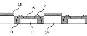
図2においてLEDチップ11やワイヤー12に干渉しないようにマスク14をセットする。そしてマスク開口からバインダーまたはバインダーリッチのスラーリーを充填又は塗布し、また必要によりバインダーの硬化を促進させた後その上に第2の蛍光体からなるスラーリーを充填又は塗布する。前記バインダーまたは第1の蛍光体とバインダーの混合体は充填又は塗布しやすくまた気泡が混入しにくいように溶媒で希釈したほうが好ましい。またより蛍光体を均一分散させるために第1蛍光体を含むスラーリーも第2の蛍光体を含むスラーリーも複数回に分けて充填又は塗布を行いうことが肝要である。バインダーまたは第1の蛍光体を含むスラーリーを充填する場合の乾燥硬化したスラーリーの充填レベルはLEDの高さの±30マイクロメートルにした方がエッジカバーを良くしトータル膜厚を少なくすることができ、空間的色温度を調整しやすくできるので好ましい。また充填後の蛍光体の沈降を防ぐためにも、いずれの混合体やスラーリーも充填又は塗布を行う都度バインダーの硬化は促進たさせた方が好ましい。
In FIG. 2, the
図3においてLED又はそれを含む基板等はバインダーまたは第1の蛍光体を含む混合体でコーティングされる。混合体には溶媒や拡散材を加えても良い。塗布装置は問わないがインパクトを付加したパルス的スプレイが好適である。
基板全体をコーティングする場合は後工程のレンズモールド樹脂の密着性を考慮すると蛍光体の含有量は重量比で50%以下が好ましく、理想的には3乃至30%が好ましい。理由はバインダーのみより蛍光体が存在するとチクソトロピック性が向上し側壁の垂れやエッジの引けが起こりにくいからである。また含有量はLEDの側面から発光する量と体積当たりの色変換により決定すべきである。またマスクをセットする際は指触乾燥程度にバインダーの硬化を促進させることが好ましい。
また第2の蛍光体とバインダーを含むスラーリーを塗布する際はマスクを基板より少し浮かせた方がマスク上のバインダーの硬化のスピードを抑えられるので回収の面からは都合がよい。通常LEDは吸着加熱テーブルで吸着して熱伝導を良くするので、吸着力を弱めることにより達成できる。充填または塗布後はすばやくマスクを除去し吸着させて30乃至120℃に加熱したテーブルからの熱伝導を上げることでバインダーの硬化を急速に促進させることができる。
In FIG. 3, an LED or a substrate including the LED is coated with a binder or a mixture including a first phosphor. A solvent or a diffusing material may be added to the mixture. Although a coating apparatus is not ask | required, the pulsed spray which added the impact is suitable.
In the case of coating the entire substrate, the phosphor content is preferably 50% or less by weight in consideration of the adhesion of the lens mold resin in the subsequent process, and ideally 3 to 30%. The reason is that if a phosphor is present rather than only a binder, thixotropic properties are improved and side wall dripping and edge shrinkage are unlikely to occur. The content should be determined by the amount of light emitted from the side of the LED and color conversion per volume. Moreover, when setting a mask, it is preferable to accelerate | stimulate hardening of a binder to the extent of touch dryness.
In addition, when applying the slurry containing the second phosphor and the binder, it is convenient from the viewpoint of recovery that the mask is slightly lifted from the substrate because the speed of curing of the binder on the mask can be suppressed. Usually, an LED is adsorbed by an adsorption heating table to improve heat conduction, and can be achieved by weakening the adsorption force. After filling or coating, the curing of the binder can be accelerated rapidly by quickly removing the mask and adsorbing it to increase the heat conduction from the table heated to 30 to 120 ° C.
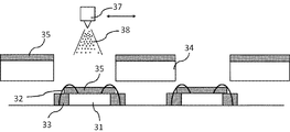
図4においてLED31の周辺、または必要によりLED上部まで充填されたバインダーまたは第1の蛍光体を含むスラーリーの塗布層の少なくとも一部とLEDの上部に第2のスラーリーを塗布器でスプレイ塗布し蛍光体層35を形成させる。塗布器はトラバースしながら蛍光体粒度分布を考慮して薄膜で3乃至15層スプレイ塗布したほうがより均一に蛍光体を分散できるので性能は向上する。LEDの色温度分布を理想的なものにするためにLEDの上部にマスク34をセットしマスク開口部と塗布領域はLEDの構造、LED周囲または上部の蛍光体の比率などにより決定すべきである。
またフィリップチップタイプを除きマスクの位置はワイヤー32より高い位置にセットすることによりハンドリングが容易になるため自動化が図れる。
In FIG. 4, the second slurry is spray-coated with an applicator on at least a part of the slurry coating layer including the binder or the first phosphor filled around the
Further, except for the Philip chip type, the mask position is set higher than the
図5はマスク44でLEDチップやワイヤ−が干渉しないように開口が形成してある。
In FIG. 5, an opening is formed in the
図6は本発明により形成された塗膜である。バインダーまたは第1の蛍光体を含むスラーリー層53は複数層でよくまた第2の蛍光体を含むスラーリー層55も複数層にした方が好ましい。バインダーが実質的に0の第2蛍光体のみのスラーリーの塗布後は振動等で蛍光体が離脱しないようにバインダーのみで薄膜でカバーコート層55の形成もできる。もちろんのこと基板全体を例えば5マイクロメートル以下にコートできる。
FIG. 6 is a coating film formed according to the present invention. The
図7は従来のディスペンサーなどにおけるLED61に蛍光体が含まれるスラーリーを塗布した略図で中央部の膜厚が厚くエッジ(edge)がカバー(cover)できないので色温度にバラツキが生じる。又塗布量が少ないとリード線62が接合されるパッド付近は陰になり塗布されにくい。
FIG. 7 is a schematic diagram in which a slurry including phosphor is applied to the
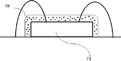
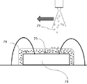
図8、図9はバインダーまたはバインダーリッチ層78に第2の蛍光体または第2の蛍光体とバインダーからなる粒子79がスプレイ流またはジェット流で衝突し潜り込むイメージを表している。
FIG. 8 and FIG. 9 show an image in which the second phosphor or the
従来技術では、例えば平均粒度分布が8マイクロメートル前後で1マイクロメートル以下から30マイクロメートルの分布をしている比重の高い蛍光体と、比重の比較的低いバインダーと、必要により加えた溶媒とからなるスラーリーを単位面積当たり±1.5%のバラツキをもって一回で薄膜塗布するのは至難の業であった。またミクロ的に見たら粒子の大きい部位と小さい部位は当然存在する。 In the prior art, for example, a phosphor having a high specific gravity having an average particle size distribution of about 8 micrometers and a distribution of 1 micrometer or less to 30 micrometers, a binder having a relatively low specific gravity, and a solvent added if necessary. It was extremely difficult to apply the slurry with a thin film at a time with a variation of ± 1.5% per unit area. From a microscopic viewpoint, there are naturally large portions and small portions of particles.
本発明では特願2011−200395の技術を第1のバインダーまたはスラーリーや第2の蛍光体を含むスラーリーの分散や充填、塗布に応用し図示しない例えばスラーリーが充填されたシリンジと塗布器と小型ポンプで循環回路を形成し、必要によりシリンジ内のスラーリーを撹拌して均一に分散させながら循環させ、又はスラーリーが充填されたシリンジを含む循環回路内に撹拌兼ポンプ機構を形成することにより塗布器に加圧流を経由させてシリンジ上流に戻して循環させ、又は二つのシリンジ間のスラーリーに差圧をもって交互に移動させ、片方のシリンジへの移動は15KPa乃至40Kpaの液圧差で流速を上げ噴流を発生させながら均一に分散させたスラーリーを吐出して薄膜で可能な限り多層に塗布する。
特にバインダーが事実上0又は極端に少ないスラーリーの分散には流速をあげて分散することが重要である。
In the present invention, the technique of Japanese Patent Application No. 2011-200395 is applied to the dispersion, filling, and coating of slurry containing the first binder or slurry and second phosphor, and a syringe, applicator, and small pump (not shown), for example, filled with slurry. In the applicator by forming a stirring and pumping mechanism in the circulation circuit including the syringe filled with the slurry. Return to the upstream of the syringe through the pressurized flow and circulate, or alternately move the slurry between the two syringes with a differential pressure, and moving to one syringe increases the flow rate with a hydraulic pressure difference of 15 KPa to 40 Kpa and generates a jet Then, the slurry which is uniformly dispersed is discharged and applied as thin as possible with a thin film.
In particular, in order to disperse slurries with virtually zero or extremely few binders, it is important to disperse by increasing the flow rate.
このようにすることにより確率の面からも塗布膜の粒度分布を均一にすることができる。更に循環回路の好ましい部位に超音波等の振動を付加することにより良好な分散状態を保つことができる。更に好適な塗膜形成ではLEDの表面を電気泳動と同じく導電性を持たせることにより、例えばスプレイ塗布の場合、霧化された粒子を静電気などで帯電させることにより静電反発で霧化粒子同士の凝集を防ぎ微粒子も付着させることができるので理想的な蛍光体塗布ができる。 By doing so, the particle size distribution of the coating film can be made uniform from the viewpoint of probability. Furthermore, a good dispersion state can be maintained by adding vibrations such as ultrasonic waves to a preferable portion of the circulation circuit. Furthermore, in the formation of a suitable coating film, the surface of the LED is made conductive as in electrophoresis. For example, in the case of spray coating, the atomized particles are electrostatically repelled by charging the atomized particles with static electricity. Therefore, it is possible to apply an ideal phosphor.
また本発明は、一種類のスラーリーを単一の塗布器で多層に塗布することに限定するものでなく、複数の塗布器で複数の蛍光体を多層塗布することも出来る。すなわち、本発明によれば、1つの塗装ブース内に複数の塗布器を設置した塗布装置を用い、種類の異なる複数の蛍光体をLEDに積層し乾燥させてLEDを製造することができる。上記少なくとも2種類の蛍光体の積層は少なくとも赤色、緑色、黄色、青色の蛍光体から選択することが出来る。 In addition, the present invention is not limited to applying a single type of slurry to multiple layers with a single applicator, and multiple phosphors can be applied in multiple layers with multiple applicators. That is, according to the present invention, an LED can be manufactured by using a coating apparatus in which a plurality of applicators are installed in one coating booth and laminating and drying a plurality of different types of phosphors on the LED. The laminate of the at least two types of phosphors can be selected from at least red, green, yellow, and blue phosphors.
また、上記少なくとも第2の蛍光体を含むスラーリーの蛍光体は少なくともバインダ−を実質的に0にまた可能な限りバインダーを少なくするようにしたスラーリーとすると回収し蛍光体の再利用の面で好適である。 In addition, the slurryy phosphor containing at least the second phosphor is preferably a slurry with at least a binder of 0 and a binder reduced as much as possible, which is suitable in terms of recovery and reuse of the phosphor. It is.
蛍光体の回収に適してさえいればマスクの寸法や形状、材質は問わないが、高性能のまま蛍光体を回収し再利用する場合は蛍光体で研磨されにくいセラミックス系材質が理想である。 The size, shape, and material of the mask are not limited as long as they are suitable for the recovery of the phosphor, but when the phosphor is recovered and reused with high performance, a ceramic material that is difficult to be polished with the phosphor is ideal.
またコンタミネーションの面からもLED表面や蛍光体に使用される材質と同じか影響を与えない例えばセラミックなどの材質が好ましい。
特にマスクを再使用し回収効率を高めるためには、マスクを建築用の外壁ボードなどに施される汚染防止などのフッ素系やセラミックス系の処理剤で被覆するとゲル化が進んだマスク上の塗膜も剥離しやすい。また高速生産向けには、例えばフッ素系やポリイミドアミド樹脂に代表されるような予め耐熱、耐溶剤性のプラスチックフィルムを基板上に部分的に或いは面に基板側にシリコーン系、架橋したアクリル系ウレタン系等の耐熱、耐溶剤性の粘着剤を施して予めラミネートすることもできる。
Also from the viewpoint of contamination, a material such as ceramic that is the same as or does not affect the material used for the LED surface or phosphor is preferable.
In particular, in order to reuse the mask and increase the recovery efficiency, coating the mask with a fluorine or ceramic treatment agent such as anti-contamination applied to building exterior wall boards, etc., causes the coating on the mask that has been gelled. The film is easy to peel off. For high-speed production, for example, a heat- and solvent-resistant plastic film, such as fluorine-based or polyimide amide resin, is partially or partially coated on the substrate with silicone-based or cross-linked acrylic urethane. It is also possible to laminate in advance by applying a heat- and solvent-resistant adhesive such as a system.
塗布器がエアスプレイあるいはエアアシストスプレイあるいは特に第2蛍光体からなるスラーリーを粒子製造装置で粒子化した後ジェット流で蛍光体粒子を搬送する場合、LED基板表面でのそれらのパターン幅は1乃至20mm程度になるようにすることが好ましい。パターン幅はチップの形状や種類によりチップ全体の所望するそれぞれの部位の膜厚を考慮して選択すべきである。LEDチップのエッジや側壁を所望する膜厚にするには、特願2011−200395によるインパクトを備えたパルス的スプレイ方法やジェット流で搬送する場合でも蛍光体粒子もジェット流もパルス的に行うとより効果的である。 When the applicator transports phosphor particles by jet flow after the sprayer is made into air spray, air-assisted spray, or particularly slurry made of the second phosphor by the particle production apparatus, the pattern width on the surface of the LED substrate is 1 to It is preferable to be about 20 mm. The pattern width should be selected in consideration of the film thickness of each desired portion of the entire chip depending on the shape and type of the chip. In order to obtain the desired film thickness on the edge and side wall of the LED chip, both the phosphor particles and the jet stream are pulsed even when transported by a pulsed spray method with impact according to Japanese Patent Application No. 2011-200395 or jet stream. More effective.
スプレイする場合などフロー性やバインダーの硬化を促進させること、スプレイなどの塗膜形成時に発生する気化熱による温度低下などを考慮してLEDを30乃至120℃の範囲に加温し、LEDとスプレイヘッドとの距離を5乃至90mmに設定し、LEDに到達する際のスプレイパターン幅を1乃至20mmとし、スプレイエア圧を0.1乃至0.4MPaでパルス的に噴出させ、パルス的にインパクトを与えながらスプレイすることが好適である。
更にシリコーンなどの濡れにくいバインダーからなるスラーリーを使用する場合には塗布材にインパクトを与えながらLED用被塗物表面に衝突させなければ特に側壁やエッジ付近をカバーするのは難しい。
Heating the LED to a range of 30 to 120 ° C. in consideration of promoting flow properties and curing of the binder when spraying, temperature decrease due to heat of vaporization generated during coating formation such as spraying, etc. The distance from the head is set to 5 to 90 mm, the spray pattern width when reaching the LED is set to 1 to 20 mm, the spray air pressure is ejected in pulses at 0.1 to 0.4 MPa, and the impact is effected in pulses. It is preferable to spray while giving.
Further, when using a slurry made of a binder such as silicone that is difficult to wet, it is difficult to cover the side walls and the edges in particular unless they impact the coating material and collide with the surface of the object to be coated for LED.
単色或いは複数色に関わらず特に第2蛍光体を含むスラーリーは層ごとに或いは必要とする層や最終層の一つ前の層で色温度や重量を測定し、必要により塗布量を補正しながら所望する品質にすることができる。 Regardless of single color or multiple colors, especially slurries containing the second phosphor measure the color temperature and weight for each layer or in the layer before the required layer or the last layer, and correct the coating amount if necessary The desired quality can be achieved.
本発明によれば特に付加価値の高いLEDを高品位に保ちながら高価な蛍光体を回収して再利用するので、従来プロセスより使用効率を10倍以上も高くできることから、大幅なコストを低減ができる。 According to the present invention, since expensive phosphors are collected and reused while keeping high value-added LEDs in high quality, the usage efficiency can be increased by 10 times or more compared with the conventional process, so the cost can be greatly reduced. it can.
1,11,21,31,41,51,61,71 LEDチップ
2,12,22,32,42,52,62 ワイヤー
3,63 蛍光体層
13,23,33,43,53 バインダー、第1蛍光体層
14,34,44 マスク
15,25,35,55 第2蛍光体層
56 バインダー(カバー層)
78 第1の蛍光体
79 第2の蛍光体
1, 11, 21, 31, 41, 51, 61, 71
78
Claims (4)
The second slurry is a slurry composed of a phosphor of a plurality of colors selected from red, green, yellow, and blue phosphors and a binder, and each of the second slurries is applied by a plurality of applicators corresponding to the slurries of each color. 4. The method for manufacturing an LED according to claim 1, wherein a plurality of thin films are applied.
Priority Applications (1)
| Application Number | Priority Date | Filing Date | Title |
|---|---|---|---|
| JP2013050950A JP6233872B2 (en) | 2013-03-13 | 2013-03-13 | LED manufacturing method |
Applications Claiming Priority (1)
| Application Number | Priority Date | Filing Date | Title |
|---|---|---|---|
| JP2013050950A JP6233872B2 (en) | 2013-03-13 | 2013-03-13 | LED manufacturing method |
Publications (3)
| Publication Number | Publication Date |
|---|---|
| JP2014179384A JP2014179384A (en) | 2014-09-25 |
| JP2014179384A5 JP2014179384A5 (en) | 2016-05-12 |
| JP6233872B2 true JP6233872B2 (en) | 2017-11-22 |
Family
ID=51699075
Family Applications (1)
| Application Number | Title | Priority Date | Filing Date |
|---|---|---|---|
| JP2013050950A Active JP6233872B2 (en) | 2013-03-13 | 2013-03-13 | LED manufacturing method |
Country Status (1)
| Country | Link |
|---|---|
| JP (1) | JP6233872B2 (en) |
Families Citing this family (2)
| Publication number | Priority date | Publication date | Assignee | Title |
|---|---|---|---|---|
| KR20170026801A (en) | 2015-08-28 | 2017-03-09 | 삼성전자주식회사 | Semiconductor light emitting device package and light source module using the same |
| JP6998114B2 (en) * | 2016-12-27 | 2022-02-04 | 日亜化学工業株式会社 | Manufacturing method of light emitting device |
Family Cites Families (9)
| Publication number | Priority date | Publication date | Assignee | Title |
|---|---|---|---|---|
| JP3434714B2 (en) * | 1998-10-20 | 2003-08-11 | 株式会社シチズン電子 | Method for manufacturing surface mount light emitting diode |
| DE10010638A1 (en) * | 2000-03-03 | 2001-09-13 | Osram Opto Semiconductors Gmbh | Making light emitting semiconducting body with luminescence conversion element involves applying suspension with solvent, adhesive, luminescent material |
| JP2002335020A (en) * | 2001-05-10 | 2002-11-22 | Nichia Chem Ind Ltd | Light emitting device |
| JP2006024615A (en) * | 2004-07-06 | 2006-01-26 | Matsushita Electric Ind Co Ltd | Led lighting source and manufacturing method thereof |
| US8058088B2 (en) * | 2008-01-15 | 2011-11-15 | Cree, Inc. | Phosphor coating systems and methods for light emitting structures and packaged light emitting diodes including phosphor coating |
| TWI381556B (en) * | 2009-03-20 | 2013-01-01 | Everlight Electronics Co Ltd | Light emitting diode package structure and manufacturing method thereof |
| TW201138976A (en) * | 2010-01-08 | 2011-11-16 | Mtek Smart Corp | Coating method and device |
| JPWO2012090961A1 (en) * | 2010-12-28 | 2014-06-05 | コニカミノルタ株式会社 | LIGHT EMITTING DEVICE, LIGHT EMITTING DEVICE MANUFACTURING METHOD, AND COATING LIQUID |
| JP5617737B2 (en) * | 2011-03-31 | 2014-11-05 | コニカミノルタ株式会社 | Light emitting device manufacturing method, light emitting device, and phosphor particle dispersion |
-
2013
- 2013-03-13 JP JP2013050950A patent/JP6233872B2/en active Active
Also Published As
| Publication number | Publication date |
|---|---|
| JP2014179384A (en) | 2014-09-25 |
Similar Documents
| Publication | Publication Date | Title |
|---|---|---|
| JP6211420B2 (en) | LED manufacturing method, LED manufacturing apparatus, and LED | |
| EP2543060B1 (en) | Methods for application of optical materials to optical elements | |
| US7569406B2 (en) | Method for coating semiconductor device using droplet deposition | |
| US9859476B2 (en) | LED production method and LEDs | |
| US20040166234A1 (en) | Apparatus and method for coating a light source to provide a modified output spectrum | |
| TW201338213A (en) | Method for manufacturing LED package | |
| CN106660065B (en) | Method for coating powder | |
| JP2015217360A (en) | Film forming device of phosphor layer and film forming method of phosphor layer | |
| JP6233872B2 (en) | LED manufacturing method | |
| CN102120213B (en) | LED fluorescent powder spraying process | |
| JP6507434B2 (en) | LED manufacturing method and LED | |
| TWI537058B (en) | LED light fluorescent powder ultrasonic spraying process | |
| US20120313120A1 (en) | Method For Depositing A Phosphor Layer On LEDs, And Apparatus Made Thereby | |
| KR101244673B1 (en) | Apparatus and method for coating phosphor | |
| KR101658446B1 (en) | Method of manufacturing luminescence powder resin film and luminescence powder resin film manufactured thereby | |
| KR100942782B1 (en) | An apparatus for coating for metal pcb for prevention of over heating of environmental friendly led board | |
| JP2016164963A (en) | Manufacturing method of light-emitting device |
Legal Events
| Date | Code | Title | Description |
|---|---|---|---|
| A521 | Request for written amendment filed |
Free format text: JAPANESE INTERMEDIATE CODE: A523 Effective date: 20160308 |
|
| A621 | Written request for application examination |
Free format text: JAPANESE INTERMEDIATE CODE: A621 Effective date: 20160309 |
|
| A977 | Report on retrieval |
Free format text: JAPANESE INTERMEDIATE CODE: A971007 Effective date: 20161116 |
|
| A131 | Notification of reasons for refusal |
Free format text: JAPANESE INTERMEDIATE CODE: A131 Effective date: 20170110 |
|
| A521 | Request for written amendment filed |
Free format text: JAPANESE INTERMEDIATE CODE: A523 Effective date: 20170303 |
|
| A131 | Notification of reasons for refusal |
Free format text: JAPANESE INTERMEDIATE CODE: A131 Effective date: 20170704 |
|
| A521 | Request for written amendment filed |
Free format text: JAPANESE INTERMEDIATE CODE: A523 Effective date: 20170831 |
|
| TRDD | Decision of grant or rejection written | ||
| A01 | Written decision to grant a patent or to grant a registration (utility model) |
Free format text: JAPANESE INTERMEDIATE CODE: A01 Effective date: 20171016 |
|
| A61 | First payment of annual fees (during grant procedure) |
Free format text: JAPANESE INTERMEDIATE CODE: A61 Effective date: 20171019 |
|
| R150 | Certificate of patent or registration of utility model |
Ref document number: 6233872 Country of ref document: JP Free format text: JAPANESE INTERMEDIATE CODE: R150 |
|
| S531 | Written request for registration of change of domicile |
Free format text: JAPANESE INTERMEDIATE CODE: R313531 |
|
| R350 | Written notification of registration of transfer |
Free format text: JAPANESE INTERMEDIATE CODE: R350 |
|
| R250 | Receipt of annual fees |
Free format text: JAPANESE INTERMEDIATE CODE: R250 |