JP6218462B2 - Wide gap semiconductor device - Google Patents
Wide gap semiconductor device Download PDFInfo
- Publication number
- JP6218462B2 JP6218462B2 JP2013140348A JP2013140348A JP6218462B2 JP 6218462 B2 JP6218462 B2 JP 6218462B2 JP 2013140348 A JP2013140348 A JP 2013140348A JP 2013140348 A JP2013140348 A JP 2013140348A JP 6218462 B2 JP6218462 B2 JP 6218462B2
- Authority
- JP
- Japan
- Prior art keywords
- gap semiconductor
- wide gap
- layer
- mosfet
- source
- Prior art date
- Legal status (The legal status is an assumption and is not a legal conclusion. Google has not performed a legal analysis and makes no representation as to the accuracy of the status listed.)
- Active
Links
- 239000004065 semiconductor Substances 0.000 title claims description 88
- 239000010410 layer Substances 0.000 claims description 146
- 238000000034 method Methods 0.000 claims description 22
- 239000002344 surface layer Substances 0.000 claims description 19
- 239000011229 interlayer Substances 0.000 claims description 17
- 230000002093 peripheral effect Effects 0.000 claims description 3
- 229910021420 polycrystalline silicon Inorganic materials 0.000 description 21
- 229920005591 polysilicon Polymers 0.000 description 21
- 230000015556 catabolic process Effects 0.000 description 13
- 238000010586 diagram Methods 0.000 description 13
- 239000012535 impurity Substances 0.000 description 10
- 230000000694 effects Effects 0.000 description 9
- 230000015572 biosynthetic process Effects 0.000 description 8
- HBMJWWWQQXIZIP-UHFFFAOYSA-N silicon carbide Chemical compound [Si+]#[C-] HBMJWWWQQXIZIP-UHFFFAOYSA-N 0.000 description 7
- 238000009792 diffusion process Methods 0.000 description 6
- 239000000463 material Substances 0.000 description 6
- 229910010271 silicon carbide Inorganic materials 0.000 description 6
- 230000003647 oxidation Effects 0.000 description 5
- 238000007254 oxidation reaction Methods 0.000 description 5
- 229910005883 NiSi Inorganic materials 0.000 description 3
- 238000005530 etching Methods 0.000 description 3
- 238000010438 heat treatment Methods 0.000 description 2
- 238000005468 ion implantation Methods 0.000 description 2
- 238000004519 manufacturing process Methods 0.000 description 2
- 150000004770 chalcogenides Chemical class 0.000 description 1
- 238000001514 detection method Methods 0.000 description 1
- 230000005669 field effect Effects 0.000 description 1
- 150000002500 ions Chemical class 0.000 description 1
- 230000001681 protective effect Effects 0.000 description 1
Images


Classifications
-
- H—ELECTRICITY
- H01—ELECTRIC ELEMENTS
- H01L—SEMICONDUCTOR DEVICES NOT COVERED BY CLASS H10
- H01L27/00—Devices consisting of a plurality of semiconductor or other solid-state components formed in or on a common substrate
- H01L27/02—Devices consisting of a plurality of semiconductor or other solid-state components formed in or on a common substrate including semiconductor components specially adapted for rectifying, oscillating, amplifying or switching and having potential barriers; including integrated passive circuit elements having potential barriers
- H01L27/0203—Particular design considerations for integrated circuits
- H01L27/0248—Particular design considerations for integrated circuits for electrical or thermal protection, e.g. electrostatic discharge [ESD] protection
- H01L27/0251—Particular design considerations for integrated circuits for electrical or thermal protection, e.g. electrostatic discharge [ESD] protection for MOS devices
-
- H—ELECTRICITY
- H01—ELECTRIC ELEMENTS
- H01L—SEMICONDUCTOR DEVICES NOT COVERED BY CLASS H10
- H01L29/00—Semiconductor devices specially adapted for rectifying, amplifying, oscillating or switching and having potential barriers; Capacitors or resistors having potential barriers, e.g. a PN-junction depletion layer or carrier concentration layer; Details of semiconductor bodies or of electrodes thereof ; Multistep manufacturing processes therefor
- H01L29/66—Types of semiconductor device ; Multistep manufacturing processes therefor
- H01L29/68—Types of semiconductor device ; Multistep manufacturing processes therefor controllable by only the electric current supplied, or only the electric potential applied, to an electrode which does not carry the current to be rectified, amplified or switched
- H01L29/76—Unipolar devices, e.g. field effect transistors
- H01L29/772—Field effect transistors
- H01L29/78—Field effect transistors with field effect produced by an insulated gate
- H01L29/7801—DMOS transistors, i.e. MISFETs with a channel accommodating body or base region adjoining a drain drift region
- H01L29/7802—Vertical DMOS transistors, i.e. VDMOS transistors
-
- H—ELECTRICITY
- H01—ELECTRIC ELEMENTS
- H01L—SEMICONDUCTOR DEVICES NOT COVERED BY CLASS H10
- H01L21/00—Processes or apparatus adapted for the manufacture or treatment of semiconductor or solid state devices or of parts thereof
- H01L21/70—Manufacture or treatment of devices consisting of a plurality of solid state components formed in or on a common substrate or of parts thereof; Manufacture of integrated circuit devices or of parts thereof
- H01L21/77—Manufacture or treatment of devices consisting of a plurality of solid state components or integrated circuits formed in, or on, a common substrate
- H01L21/78—Manufacture or treatment of devices consisting of a plurality of solid state components or integrated circuits formed in, or on, a common substrate with subsequent division of the substrate into plural individual devices
- H01L21/82—Manufacture or treatment of devices consisting of a plurality of solid state components or integrated circuits formed in, or on, a common substrate with subsequent division of the substrate into plural individual devices to produce devices, e.g. integrated circuits, each consisting of a plurality of components
- H01L21/8213—Manufacture or treatment of devices consisting of a plurality of solid state components or integrated circuits formed in, or on, a common substrate with subsequent division of the substrate into plural individual devices to produce devices, e.g. integrated circuits, each consisting of a plurality of components the substrate being a semiconductor, using SiC technology
-
- H—ELECTRICITY
- H01—ELECTRIC ELEMENTS
- H01L—SEMICONDUCTOR DEVICES NOT COVERED BY CLASS H10
- H01L21/00—Processes or apparatus adapted for the manufacture or treatment of semiconductor or solid state devices or of parts thereof
- H01L21/70—Manufacture or treatment of devices consisting of a plurality of solid state components formed in or on a common substrate or of parts thereof; Manufacture of integrated circuit devices or of parts thereof
- H01L21/77—Manufacture or treatment of devices consisting of a plurality of solid state components or integrated circuits formed in, or on, a common substrate
- H01L21/78—Manufacture or treatment of devices consisting of a plurality of solid state components or integrated circuits formed in, or on, a common substrate with subsequent division of the substrate into plural individual devices
- H01L21/82—Manufacture or treatment of devices consisting of a plurality of solid state components or integrated circuits formed in, or on, a common substrate with subsequent division of the substrate into plural individual devices to produce devices, e.g. integrated circuits, each consisting of a plurality of components
- H01L21/8252—Manufacture or treatment of devices consisting of a plurality of solid state components or integrated circuits formed in, or on, a common substrate with subsequent division of the substrate into plural individual devices to produce devices, e.g. integrated circuits, each consisting of a plurality of components the substrate being a semiconductor, using III-V technology
-
- H—ELECTRICITY
- H01—ELECTRIC ELEMENTS
- H01L—SEMICONDUCTOR DEVICES NOT COVERED BY CLASS H10
- H01L27/00—Devices consisting of a plurality of semiconductor or other solid-state components formed in or on a common substrate
- H01L27/02—Devices consisting of a plurality of semiconductor or other solid-state components formed in or on a common substrate including semiconductor components specially adapted for rectifying, oscillating, amplifying or switching and having potential barriers; including integrated passive circuit elements having potential barriers
- H01L27/04—Devices consisting of a plurality of semiconductor or other solid-state components formed in or on a common substrate including semiconductor components specially adapted for rectifying, oscillating, amplifying or switching and having potential barriers; including integrated passive circuit elements having potential barriers the substrate being a semiconductor body
- H01L27/06—Devices consisting of a plurality of semiconductor or other solid-state components formed in or on a common substrate including semiconductor components specially adapted for rectifying, oscillating, amplifying or switching and having potential barriers; including integrated passive circuit elements having potential barriers the substrate being a semiconductor body including a plurality of individual components in a non-repetitive configuration
- H01L27/0605—Devices consisting of a plurality of semiconductor or other solid-state components formed in or on a common substrate including semiconductor components specially adapted for rectifying, oscillating, amplifying or switching and having potential barriers; including integrated passive circuit elements having potential barriers the substrate being a semiconductor body including a plurality of individual components in a non-repetitive configuration integrated circuits made of compound material, e.g. AIIIBV
-
- H—ELECTRICITY
- H01—ELECTRIC ELEMENTS
- H01L—SEMICONDUCTOR DEVICES NOT COVERED BY CLASS H10
- H01L27/00—Devices consisting of a plurality of semiconductor or other solid-state components formed in or on a common substrate
- H01L27/02—Devices consisting of a plurality of semiconductor or other solid-state components formed in or on a common substrate including semiconductor components specially adapted for rectifying, oscillating, amplifying or switching and having potential barriers; including integrated passive circuit elements having potential barriers
- H01L27/04—Devices consisting of a plurality of semiconductor or other solid-state components formed in or on a common substrate including semiconductor components specially adapted for rectifying, oscillating, amplifying or switching and having potential barriers; including integrated passive circuit elements having potential barriers the substrate being a semiconductor body
- H01L27/08—Devices consisting of a plurality of semiconductor or other solid-state components formed in or on a common substrate including semiconductor components specially adapted for rectifying, oscillating, amplifying or switching and having potential barriers; including integrated passive circuit elements having potential barriers the substrate being a semiconductor body including only semiconductor components of a single kind
- H01L27/085—Devices consisting of a plurality of semiconductor or other solid-state components formed in or on a common substrate including semiconductor components specially adapted for rectifying, oscillating, amplifying or switching and having potential barriers; including integrated passive circuit elements having potential barriers the substrate being a semiconductor body including only semiconductor components of a single kind including field-effect components only
- H01L27/088—Devices consisting of a plurality of semiconductor or other solid-state components formed in or on a common substrate including semiconductor components specially adapted for rectifying, oscillating, amplifying or switching and having potential barriers; including integrated passive circuit elements having potential barriers the substrate being a semiconductor body including only semiconductor components of a single kind including field-effect components only the components being field-effect transistors with insulated gate
-
- H—ELECTRICITY
- H01—ELECTRIC ELEMENTS
- H01L—SEMICONDUCTOR DEVICES NOT COVERED BY CLASS H10
- H01L29/00—Semiconductor devices specially adapted for rectifying, amplifying, oscillating or switching and having potential barriers; Capacitors or resistors having potential barriers, e.g. a PN-junction depletion layer or carrier concentration layer; Details of semiconductor bodies or of electrodes thereof ; Multistep manufacturing processes therefor
- H01L29/66—Types of semiconductor device ; Multistep manufacturing processes therefor
- H01L29/66007—Multistep manufacturing processes
- H01L29/66053—Multistep manufacturing processes of devices having a semiconductor body comprising crystalline silicon carbide
- H01L29/66068—Multistep manufacturing processes of devices having a semiconductor body comprising crystalline silicon carbide the devices being controllable only by the electric current supplied or the electric potential applied, to an electrode which does not carry the current to be rectified, amplified or switched, e.g. three-terminal devices
-
- H—ELECTRICITY
- H01—ELECTRIC ELEMENTS
- H01L—SEMICONDUCTOR DEVICES NOT COVERED BY CLASS H10
- H01L29/00—Semiconductor devices specially adapted for rectifying, amplifying, oscillating or switching and having potential barriers; Capacitors or resistors having potential barriers, e.g. a PN-junction depletion layer or carrier concentration layer; Details of semiconductor bodies or of electrodes thereof ; Multistep manufacturing processes therefor
- H01L29/66—Types of semiconductor device ; Multistep manufacturing processes therefor
- H01L29/66007—Multistep manufacturing processes
- H01L29/66075—Multistep manufacturing processes of devices having semiconductor bodies comprising group 14 or group 13/15 materials
- H01L29/66227—Multistep manufacturing processes of devices having semiconductor bodies comprising group 14 or group 13/15 materials the devices being controllable only by the electric current supplied or the electric potential applied, to an electrode which does not carry the current to be rectified, amplified or switched, e.g. three-terminal devices
- H01L29/66409—Unipolar field-effect transistors
- H01L29/66477—Unipolar field-effect transistors with an insulated gate, i.e. MISFET
- H01L29/66674—DMOS transistors, i.e. MISFETs with a channel accommodating body or base region adjoining a drain drift region
- H01L29/66712—Vertical DMOS transistors, i.e. VDMOS transistors
-
- H—ELECTRICITY
- H01—ELECTRIC ELEMENTS
- H01L—SEMICONDUCTOR DEVICES NOT COVERED BY CLASS H10
- H01L29/00—Semiconductor devices specially adapted for rectifying, amplifying, oscillating or switching and having potential barriers; Capacitors or resistors having potential barriers, e.g. a PN-junction depletion layer or carrier concentration layer; Details of semiconductor bodies or of electrodes thereof ; Multistep manufacturing processes therefor
- H01L29/66—Types of semiconductor device ; Multistep manufacturing processes therefor
- H01L29/68—Types of semiconductor device ; Multistep manufacturing processes therefor controllable by only the electric current supplied, or only the electric potential applied, to an electrode which does not carry the current to be rectified, amplified or switched
- H01L29/76—Unipolar devices, e.g. field effect transistors
- H01L29/772—Field effect transistors
- H01L29/78—Field effect transistors with field effect produced by an insulated gate
- H01L29/7801—DMOS transistors, i.e. MISFETs with a channel accommodating body or base region adjoining a drain drift region
- H01L29/7802—Vertical DMOS transistors, i.e. VDMOS transistors
- H01L29/7803—Vertical DMOS transistors, i.e. VDMOS transistors structurally associated with at least one other device
-
- H—ELECTRICITY
- H01—ELECTRIC ELEMENTS
- H01L—SEMICONDUCTOR DEVICES NOT COVERED BY CLASS H10
- H01L29/00—Semiconductor devices specially adapted for rectifying, amplifying, oscillating or switching and having potential barriers; Capacitors or resistors having potential barriers, e.g. a PN-junction depletion layer or carrier concentration layer; Details of semiconductor bodies or of electrodes thereof ; Multistep manufacturing processes therefor
- H01L29/66—Types of semiconductor device ; Multistep manufacturing processes therefor
- H01L29/68—Types of semiconductor device ; Multistep manufacturing processes therefor controllable by only the electric current supplied, or only the electric potential applied, to an electrode which does not carry the current to be rectified, amplified or switched
- H01L29/76—Unipolar devices, e.g. field effect transistors
- H01L29/772—Field effect transistors
- H01L29/78—Field effect transistors with field effect produced by an insulated gate
- H01L29/7801—DMOS transistors, i.e. MISFETs with a channel accommodating body or base region adjoining a drain drift region
- H01L29/7802—Vertical DMOS transistors, i.e. VDMOS transistors
- H01L29/7809—Vertical DMOS transistors, i.e. VDMOS transistors having both source and drain contacts on the same surface, i.e. Up-Drain VDMOS transistors
-
- H—ELECTRICITY
- H01—ELECTRIC ELEMENTS
- H01L—SEMICONDUCTOR DEVICES NOT COVERED BY CLASS H10
- H01L29/00—Semiconductor devices specially adapted for rectifying, amplifying, oscillating or switching and having potential barriers; Capacitors or resistors having potential barriers, e.g. a PN-junction depletion layer or carrier concentration layer; Details of semiconductor bodies or of electrodes thereof ; Multistep manufacturing processes therefor
- H01L29/66—Types of semiconductor device ; Multistep manufacturing processes therefor
- H01L29/68—Types of semiconductor device ; Multistep manufacturing processes therefor controllable by only the electric current supplied, or only the electric potential applied, to an electrode which does not carry the current to be rectified, amplified or switched
- H01L29/76—Unipolar devices, e.g. field effect transistors
- H01L29/772—Field effect transistors
- H01L29/78—Field effect transistors with field effect produced by an insulated gate
- H01L29/7801—DMOS transistors, i.e. MISFETs with a channel accommodating body or base region adjoining a drain drift region
- H01L29/7802—Vertical DMOS transistors, i.e. VDMOS transistors
- H01L29/7811—Vertical DMOS transistors, i.e. VDMOS transistors with an edge termination structure
-
- H—ELECTRICITY
- H01—ELECTRIC ELEMENTS
- H01L—SEMICONDUCTOR DEVICES NOT COVERED BY CLASS H10
- H01L29/00—Semiconductor devices specially adapted for rectifying, amplifying, oscillating or switching and having potential barriers; Capacitors or resistors having potential barriers, e.g. a PN-junction depletion layer or carrier concentration layer; Details of semiconductor bodies or of electrodes thereof ; Multistep manufacturing processes therefor
- H01L29/66—Types of semiconductor device ; Multistep manufacturing processes therefor
- H01L29/68—Types of semiconductor device ; Multistep manufacturing processes therefor controllable by only the electric current supplied, or only the electric potential applied, to an electrode which does not carry the current to be rectified, amplified or switched
- H01L29/76—Unipolar devices, e.g. field effect transistors
- H01L29/772—Field effect transistors
- H01L29/78—Field effect transistors with field effect produced by an insulated gate
- H01L29/7801—DMOS transistors, i.e. MISFETs with a channel accommodating body or base region adjoining a drain drift region
- H01L29/7802—Vertical DMOS transistors, i.e. VDMOS transistors
- H01L29/7812—Vertical DMOS transistors, i.e. VDMOS transistors with a substrate comprising an insulating layer, e.g. SOI-VDMOS transistors
-
- H—ELECTRICITY
- H01—ELECTRIC ELEMENTS
- H01L—SEMICONDUCTOR DEVICES NOT COVERED BY CLASS H10
- H01L29/00—Semiconductor devices specially adapted for rectifying, amplifying, oscillating or switching and having potential barriers; Capacitors or resistors having potential barriers, e.g. a PN-junction depletion layer or carrier concentration layer; Details of semiconductor bodies or of electrodes thereof ; Multistep manufacturing processes therefor
- H01L29/66—Types of semiconductor device ; Multistep manufacturing processes therefor
- H01L29/68—Types of semiconductor device ; Multistep manufacturing processes therefor controllable by only the electric current supplied, or only the electric potential applied, to an electrode which does not carry the current to be rectified, amplified or switched
- H01L29/76—Unipolar devices, e.g. field effect transistors
- H01L29/772—Field effect transistors
- H01L29/78—Field effect transistors with field effect produced by an insulated gate
- H01L29/7801—DMOS transistors, i.e. MISFETs with a channel accommodating body or base region adjoining a drain drift region
- H01L29/7802—Vertical DMOS transistors, i.e. VDMOS transistors
- H01L29/7815—Vertical DMOS transistors, i.e. VDMOS transistors with voltage or current sensing structure, e.g. emulator section, overcurrent sensing cell
-
- H—ELECTRICITY
- H01—ELECTRIC ELEMENTS
- H01L—SEMICONDUCTOR DEVICES NOT COVERED BY CLASS H10
- H01L2224/00—Indexing scheme for arrangements for connecting or disconnecting semiconductor or solid-state bodies and methods related thereto as covered by H01L24/00
- H01L2224/01—Means for bonding being attached to, or being formed on, the surface to be connected, e.g. chip-to-package, die-attach, "first-level" interconnects; Manufacturing methods related thereto
- H01L2224/02—Bonding areas; Manufacturing methods related thereto
- H01L2224/04—Structure, shape, material or disposition of the bonding areas prior to the connecting process
- H01L2224/06—Structure, shape, material or disposition of the bonding areas prior to the connecting process of a plurality of bonding areas
- H01L2224/0601—Structure
- H01L2224/0603—Bonding areas having different sizes, e.g. different heights or widths
-
- H—ELECTRICITY
- H01—ELECTRIC ELEMENTS
- H01L—SEMICONDUCTOR DEVICES NOT COVERED BY CLASS H10
- H01L29/00—Semiconductor devices specially adapted for rectifying, amplifying, oscillating or switching and having potential barriers; Capacitors or resistors having potential barriers, e.g. a PN-junction depletion layer or carrier concentration layer; Details of semiconductor bodies or of electrodes thereof ; Multistep manufacturing processes therefor
- H01L29/02—Semiconductor bodies ; Multistep manufacturing processes therefor
- H01L29/06—Semiconductor bodies ; Multistep manufacturing processes therefor characterised by their shape; characterised by the shapes, relative sizes, or dispositions of the semiconductor regions ; characterised by the concentration or distribution of impurities within semiconductor regions
- H01L29/0603—Semiconductor bodies ; Multistep manufacturing processes therefor characterised by their shape; characterised by the shapes, relative sizes, or dispositions of the semiconductor regions ; characterised by the concentration or distribution of impurities within semiconductor regions characterised by particular constructional design considerations, e.g. for preventing surface leakage, for controlling electric field concentration or for internal isolations regions
- H01L29/0607—Semiconductor bodies ; Multistep manufacturing processes therefor characterised by their shape; characterised by the shapes, relative sizes, or dispositions of the semiconductor regions ; characterised by the concentration or distribution of impurities within semiconductor regions characterised by particular constructional design considerations, e.g. for preventing surface leakage, for controlling electric field concentration or for internal isolations regions for preventing surface leakage or controlling electric field concentration
- H01L29/0611—Semiconductor bodies ; Multistep manufacturing processes therefor characterised by their shape; characterised by the shapes, relative sizes, or dispositions of the semiconductor regions ; characterised by the concentration or distribution of impurities within semiconductor regions characterised by particular constructional design considerations, e.g. for preventing surface leakage, for controlling electric field concentration or for internal isolations regions for preventing surface leakage or controlling electric field concentration for increasing or controlling the breakdown voltage of reverse biased devices
- H01L29/0615—Semiconductor bodies ; Multistep manufacturing processes therefor characterised by their shape; characterised by the shapes, relative sizes, or dispositions of the semiconductor regions ; characterised by the concentration or distribution of impurities within semiconductor regions characterised by particular constructional design considerations, e.g. for preventing surface leakage, for controlling electric field concentration or for internal isolations regions for preventing surface leakage or controlling electric field concentration for increasing or controlling the breakdown voltage of reverse biased devices by the doping profile or the shape or the arrangement of the PN junction, or with supplementary regions, e.g. junction termination extension [JTE]
- H01L29/0619—Semiconductor bodies ; Multistep manufacturing processes therefor characterised by their shape; characterised by the shapes, relative sizes, or dispositions of the semiconductor regions ; characterised by the concentration or distribution of impurities within semiconductor regions characterised by particular constructional design considerations, e.g. for preventing surface leakage, for controlling electric field concentration or for internal isolations regions for preventing surface leakage or controlling electric field concentration for increasing or controlling the breakdown voltage of reverse biased devices by the doping profile or the shape or the arrangement of the PN junction, or with supplementary regions, e.g. junction termination extension [JTE] with a supplementary region doped oppositely to or in rectifying contact with the semiconductor containing or contacting region, e.g. guard rings with PN or Schottky junction
-
- H—ELECTRICITY
- H01—ELECTRIC ELEMENTS
- H01L—SEMICONDUCTOR DEVICES NOT COVERED BY CLASS H10
- H01L29/00—Semiconductor devices specially adapted for rectifying, amplifying, oscillating or switching and having potential barriers; Capacitors or resistors having potential barriers, e.g. a PN-junction depletion layer or carrier concentration layer; Details of semiconductor bodies or of electrodes thereof ; Multistep manufacturing processes therefor
- H01L29/02—Semiconductor bodies ; Multistep manufacturing processes therefor
- H01L29/06—Semiconductor bodies ; Multistep manufacturing processes therefor characterised by their shape; characterised by the shapes, relative sizes, or dispositions of the semiconductor regions ; characterised by the concentration or distribution of impurities within semiconductor regions
- H01L29/0684—Semiconductor bodies ; Multistep manufacturing processes therefor characterised by their shape; characterised by the shapes, relative sizes, or dispositions of the semiconductor regions ; characterised by the concentration or distribution of impurities within semiconductor regions characterised by the shape, relative sizes or dispositions of the semiconductor regions or junctions between the regions
- H01L29/0692—Surface layout
- H01L29/0696—Surface layout of cellular field-effect devices, e.g. multicellular DMOS transistors or IGBTs
-
- H—ELECTRICITY
- H01—ELECTRIC ELEMENTS
- H01L—SEMICONDUCTOR DEVICES NOT COVERED BY CLASS H10
- H01L29/00—Semiconductor devices specially adapted for rectifying, amplifying, oscillating or switching and having potential barriers; Capacitors or resistors having potential barriers, e.g. a PN-junction depletion layer or carrier concentration layer; Details of semiconductor bodies or of electrodes thereof ; Multistep manufacturing processes therefor
- H01L29/02—Semiconductor bodies ; Multistep manufacturing processes therefor
- H01L29/12—Semiconductor bodies ; Multistep manufacturing processes therefor characterised by the materials of which they are formed
- H01L29/16—Semiconductor bodies ; Multistep manufacturing processes therefor characterised by the materials of which they are formed including, apart from doping materials or other impurities, only elements of Group IV of the Periodic Table
- H01L29/1608—Silicon carbide
-
- H—ELECTRICITY
- H01—ELECTRIC ELEMENTS
- H01L—SEMICONDUCTOR DEVICES NOT COVERED BY CLASS H10
- H01L29/00—Semiconductor devices specially adapted for rectifying, amplifying, oscillating or switching and having potential barriers; Capacitors or resistors having potential barriers, e.g. a PN-junction depletion layer or carrier concentration layer; Details of semiconductor bodies or of electrodes thereof ; Multistep manufacturing processes therefor
- H01L29/02—Semiconductor bodies ; Multistep manufacturing processes therefor
- H01L29/12—Semiconductor bodies ; Multistep manufacturing processes therefor characterised by the materials of which they are formed
- H01L29/20—Semiconductor bodies ; Multistep manufacturing processes therefor characterised by the materials of which they are formed including, apart from doping materials or other impurities, only AIIIBV compounds
- H01L29/2003—Nitride compounds
-
- H—ELECTRICITY
- H01—ELECTRIC ELEMENTS
- H01L—SEMICONDUCTOR DEVICES NOT COVERED BY CLASS H10
- H01L29/00—Semiconductor devices specially adapted for rectifying, amplifying, oscillating or switching and having potential barriers; Capacitors or resistors having potential barriers, e.g. a PN-junction depletion layer or carrier concentration layer; Details of semiconductor bodies or of electrodes thereof ; Multistep manufacturing processes therefor
- H01L29/40—Electrodes ; Multistep manufacturing processes therefor
- H01L29/402—Field plates
Landscapes
- Engineering & Computer Science (AREA)
- Power Engineering (AREA)
- Microelectronics & Electronic Packaging (AREA)
- General Physics & Mathematics (AREA)
- Computer Hardware Design (AREA)
- Physics & Mathematics (AREA)
- Condensed Matter Physics & Semiconductors (AREA)
- Ceramic Engineering (AREA)
- Manufacturing & Machinery (AREA)
- Chemical & Material Sciences (AREA)
- Crystallography & Structural Chemistry (AREA)
- Metal-Oxide And Bipolar Metal-Oxide Semiconductor Integrated Circuits (AREA)
- Electrodes Of Semiconductors (AREA)
- Semiconductor Integrated Circuits (AREA)
- Insulated Gate Type Field-Effect Transistor (AREA)
Description
本発明は、インバータ装置等を形成するMOSFET(Metal−Oxide−Semiconductor Field−Effect Transistor)等のワイドギャップ半導体装置に関するものである。 The present invention relates to a wide gap semiconductor device such as a MOSFET (Metal-Oxide-Semiconductor Field-Effect Transistor) that forms an inverter device or the like.
ワイドギャップ半導体装置の一例である、材料にSiCウェハを用いたMOSFET(以下、SiC−MOSFETと記載)は、ユニットセルが同一チップ内に複数配置されて構成される。 A MOSFET (hereinafter, referred to as SiC-MOSFET) using a SiC wafer as a material, which is an example of a wide gap semiconductor device, is configured by arranging a plurality of unit cells in the same chip.
ここで、ワイドギャップ半導体とは、一般に、およそ2eV以上の禁制帯幅をもつ半導体を指し、GaNに代表される3族窒化物、ZnOに代表される2族窒化物、ZnSeに代表される2族カルコゲナイドおよびSiC等が知られている。 Here, the wide gap semiconductor generally refers to a semiconductor having a forbidden band width of about 2 eV or more. The group chalcogenides and SiC are known.
SiC−MOSFETでは、Siウェハを用いたMOSFET(以下、Si−MOSFETと記載)の場合よりも、ドレイン電極とソース電極との間の順方向電圧降下(オン電圧)を低減することができるためユニットセル数を少なくでき、チップサイズをシュリンクすることができる(特許文献1参照)。 In the SiC-MOSFET, the forward voltage drop (on voltage) between the drain electrode and the source electrode can be reduced as compared with the MOSFET using the Si wafer (hereinafter referred to as Si-MOSFET), so that the unit The number of cells can be reduced, and the chip size can be shrunk (see Patent Document 1).
前述の通り、SiC−MOSFETでは、Si−MOSFETと比較して、チップサイズをシュリンクすることができる。しかし一方で、ゲート電極とソース電極との間の容量が小さくなり、ゲート電極とソース電極との間の静電破壊耐量が低下する問題があった。 As described above, the SiC-MOSFET can shrink the chip size as compared with the Si-MOSFET. On the other hand, however, there is a problem that the capacitance between the gate electrode and the source electrode is reduced, and the electrostatic breakdown resistance between the gate electrode and the source electrode is reduced.
Si−MOSFETでは、一般的な静電破壊対策として、ユニットセル形成時のソース工程(n型拡散層形成)とP+拡散工程(p型拡散層形成)とを用いて、ポリシリコン(Poly−Si)上にpn接合を形成し、ツエナーDiodeを内蔵させることが多い。 In a Si-MOSFET, as a general countermeasure against electrostatic breakdown, polysilicon (Poly-Si) is formed by using a source process (n-type diffusion layer formation) and a P + diffusion process (p-type diffusion layer formation) at the time of unit cell formation. In many cases, a pn junction is formed thereon and a Zener Diode is incorporated.
SiC−MOSFETでは、p型不純物およびn型不純物を活性化させるために、1500℃以上の熱処理をウェハプロセスで実施する必要があり、一般的には、ポリシリコンを形成する工程より前に、p型不純物およびn型不純物のイオン注入を実施している。 In the SiC-MOSFET, in order to activate the p-type impurity and the n-type impurity, it is necessary to perform a heat treatment at 1500 ° C. or higher in the wafer process. Generally, before the step of forming polysilicon, p Ion implantation of n-type impurities and n-type impurities is performed.
そのため、SiC−MOSFETでツエナーDiodeを内蔵させるためには、ウェハプロセス工程中において、ユニットセル形成とは別の工程でpn接合を形成する必要があり、チップ加工費が増加しチップコストが高くなるという問題があった。 Therefore, in order to incorporate the Zener Diode in the SiC-MOSFET, it is necessary to form a pn junction in a process different from the unit cell formation in the wafer process, which increases the chip processing cost and increases the chip cost. There was a problem.
本発明は、上記のような問題を解決するためになされたものであり、チップコストを増加させずに、ゲート電極とソース電極との間の静電破壊を抑制することができるワイドギャップ半導体装置を提供することを目的とする。 The present invention has been made to solve the above problems, and a wide gap semiconductor device capable of suppressing electrostatic breakdown between a gate electrode and a source electrode without increasing the chip cost. The purpose is to provide.
本発明の一態様に関するワイドギャップ半導体装置は、第1導電型のワイドギャップ半導体層表層に形成された、第2導電型の第1ベース層と、前記第1ベース層表層に形成された、第1導電型の第1ソース層と、前記第1ソース層と前記ワイドギャップ半導体層とに挟まれた前記第1ベース層上に形成されたゲート絶縁膜と、前記ゲート絶縁膜上に形成された第1ゲート電極と、前記第1ゲート電極を覆って形成された層間絶縁膜と、前記層間絶縁膜、前記第1ベース層および前記第1ソース層を覆って形成された第1ソース電極と、前記ワイドギャップ半導体層下に形成されたドレイン電極とを備える縦型ワイドギャップ半導体MOSFETと、前記ワイドギャップ半導体層表層に、前記第1ベース層と同一工程で形成された第2ベース層と、前記第2ベース層上に形成されたフィールド絶縁膜と、前記第2ベース層表層において形成され、前記第2ベース層上に形成された前記フィールド絶縁膜を平面視において挟んで位置し、かつ、前記第1ソース層と同一工程で形成された第2ソース層と、少なくとも前記フィールド絶縁膜上に形成された、前記第1ゲート電極と同一層である第2ゲート電極と、一方の前記第2ソース層上に形成され、前記第2ゲート電極と電気的に接続された第3ゲート電極と、他方の前記第2ソース層上に形成された第2ソース電極とを備える横型ワイドギャップ半導体MOSFETとを備え、前記第1ゲート電極と前記第2ゲート電極とが電気的に接続され、前記第1ソース電極と前記第2ソース電極とが電気的に接続されることを特徴とする。
A wide gap semiconductor device according to an aspect of the present invention includes a first base layer of a second conductivity type formed on a surface layer of a wide gap semiconductor layer of a first conductivity type, and a first base layer formed of a surface layer of the first base layer. A first source layer of one conductivity type, a gate insulating film formed on the first base layer sandwiched between the first source layer and the wide gap semiconductor layer, and formed on the gate insulating film A first gate electrode; an interlayer insulating film formed to cover the first gate electrode; a first source electrode formed to cover the interlayer insulating film, the first base layer and the first source layer; A vertical wide gap semiconductor MOSFET having a drain electrode formed under the wide gap semiconductor layer, and a second base formed on the surface layer of the wide gap semiconductor layer in the same step as the first base layer. When a field insulating film formed on said second base layer, is formed in the second base layer surface, the field insulating film formed on the second base layer positioned across in a plan view, And a second source layer formed in the same step as the first source layer, a second gate electrode formed on at least the field insulating film and the same layer as the first gate electrode, A lateral wide gap semiconductor comprising a third gate electrode formed on a second source layer and electrically connected to the second gate electrode, and a second source electrode formed on the other second source layer and a MOSFET, the first gate electrode and the second gate electrode are electrically connected, the first source electrode and the second source electrode and said Rukoto are electrically connected.
本発明の上記態様によれば、縦型ワイドギャップ半導体MOSFETのゲート電極とソース電極との間に正の過電圧が印加されたときに、横型ワイドギャップ半導体MOSFETのチャネルが開き、横型nチャネルMOSFET側に過電圧によるゲート電流を流すことができる。よって、チップコストを増加させずに、SiC−MOSFETのゲート電極とソース電極との間の正側の静電破壊を抑制することができる。 According to the above aspect of the present invention, when a positive overvoltage is applied between the gate electrode and the source electrode of the vertical wide gap semiconductor MOSFET, the channel of the horizontal wide gap semiconductor MOSFET opens, and the lateral n channel MOSFET side A gate current due to an overvoltage can be passed through. Therefore, electrostatic breakdown on the positive side between the gate electrode and the source electrode of the SiC-MOSFET can be suppressed without increasing the chip cost.
以下、添付の図面を参照しながら実施形態について説明する。 Hereinafter, embodiments will be described with reference to the accompanying drawings.
図17および図18に、前提技術に関するワイドギャップ半導体装置である炭化珪素(SiC)半導体装置の一例として、材料にSiCウェハを用いた縦型のMOSFET(以下、SiC−MOSFETと記載)の回路図(図17参照)およびユニットセル(活性領域)の断面概略図(図18参照)を示す。なお、用いられる半導体材料は、ワイドギャップ半導体であればよく、例えばGaN等であってもよい。 FIG. 17 and FIG. 18 are circuit diagrams of vertical MOSFETs (hereinafter referred to as SiC-MOSFETs) using a SiC wafer as a material as an example of a silicon carbide (SiC) semiconductor device which is a wide gap semiconductor device related to the base technology. (Refer FIG. 17) and the cross-sectional schematic (refer FIG. 18) of a unit cell (active region) are shown. In addition, the semiconductor material used should just be a wide gap semiconductor, for example, GaN etc. may be sufficient as it.
材料にSiCウェハを用いたMOSFET(以下、SiC−MOSFETと記載)は、図18に示されるように、ユニットセルが同一チップ内に複数配置されて構成される。 As shown in FIG. 18, a MOSFET using a SiC wafer as a material (hereinafter referred to as SiC-MOSFET) is configured by arranging a plurality of unit cells in the same chip.
具体的には、ワイドギャップ半導体層として、n型のn+バッファ層1上にn−層2が形成され、n−層2表層に、p型のpベース層3(第1ベース層)が形成される。
Specifically, an n−
さらに、pベース層3表層にはn+ソース層4(第1ソース層)が形成され、少なくともn+ソース層4とn−層2とに挟まれたpベース層3上にゲート酸化膜6(ゲート絶縁膜)が形成されている。
Further, an n + source layer 4 (first source layer) is formed on the surface layer of the
また、ゲート酸化膜6上にはゲートポリシリコン7(第1ゲート電極)が形成されている。当該ゲートポリシリコン7は、層間絶縁膜8に覆われている。
A gate polysilicon 7 (first gate electrode) is formed on the
そして、層間絶縁膜8、pベース層3およびn+ソース層4を覆って、ソース電極9が形成されている。
A
一方で、n+バッファ層1下には、ドレイン電極10が形成されている。
On the other hand, a
なお、pベース層3上において、n+ソース層4に囲まれたp+層5、および、p+層5および一部のn+ソース層4を覆って形成されたNiSi層13をさらに備えることができる。
On the
SiC−MOSFETでは、Siウェハを用いたMOSFET(以下、Si−MOSFETと記載)の場合よりも、ドレイン電極とソース電極との間の順方向電圧降下(オン電圧)を低減することができるためユニットセル数を少なくでき、チップサイズをシュリンクすることができる。 In the SiC-MOSFET, the forward voltage drop (on voltage) between the drain electrode and the source electrode can be reduced as compared with the MOSFET using the Si wafer (hereinafter referred to as Si-MOSFET), so that the unit The number of cells can be reduced, and the chip size can be shrunk.
しかし一方で、ゲート電極とソース電極との間の容量が小さくなり、ゲート電極とソース電極との間の静電破壊耐量が低下する問題があった。 On the other hand, however, there is a problem that the capacitance between the gate electrode and the source electrode is reduced, and the electrostatic breakdown resistance between the gate electrode and the source electrode is reduced.
一般的な静電破壊対策としては、ユニットセル形成時のソース工程(n型拡散層形成)とP+拡散工程(p型拡散層形成)とを用いて、ポリシリコン(Poly−Si)上にpn接合を形成し、ツエナーDiodeを内蔵させることが多い。 As a general countermeasure against electrostatic breakdown, a source process (n-type diffusion layer formation) and a P + diffusion process (p-type diffusion layer formation) at the time of unit cell formation are used to form pn on polysilicon (Poly-Si). In many cases, a junction is formed and a Zener Diode is incorporated.
しかしSiC−MOSFETにおいてツエナーDiodeを内蔵させようとする場合、p型不純物およびn型不純物を活性化させるために1500℃以上の熱処理をウェハプロセスで実施する必要があり、一般的には、ポリシリコンを形成する工程より前に、p型不純物およびn型不純物のイオン注入を実施している。 However, when incorporating a Zener Diode in an SiC-MOSFET, it is necessary to perform a heat treatment at 1500 ° C. or higher in a wafer process in order to activate the p-type impurity and the n-type impurity. Prior to the step of forming p-type impurities, ion implantation of p-type impurities and n-type impurities is performed.
そのため、SiC−MOSFETでツエナーDiodeを内蔵させるためには、ウェハプロセス工程中において、ユニットセル形成とは別の工程でpn接合を形成する必要があり、チップ加工費が増加しチップコストが高くなるという問題があった。 Therefore, in order to incorporate the Zener Diode in the SiC-MOSFET, it is necessary to form a pn junction in a process different from the unit cell formation in the wafer process, which increases the chip processing cost and increases the chip cost. There was a problem.
以下に説明する実施形態は、上記のような問題を解決するワイドギャップ半導体装置に関するものである。 The embodiment described below relates to a wide gap semiconductor device that solves the above problems.
<第1実施形態>
<構成>
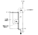
図1に、SiC−MOSFETのゲート電極とソース電極との間に、横型のnチャネルMOSFETを内蔵させた、ワイドギャップ半導体装置の回路図を示す。
<First Embodiment>
<Configuration>
FIG. 1 shows a circuit diagram of a wide gap semiconductor device in which a lateral n-channel MOSFET is built between a gate electrode and a source electrode of a SiC-MOSFET.
図1に示されるように、SiC−MOSFETに、横型nチャネルMOSFETが内蔵されている。すなわち、SiC−MOSFETのゲート電極側に、横型nチャネルMOSFETのドレインおよびゲート電極が接続されている。 As shown in FIG. 1, a lateral n-channel MOSFET is built in the SiC-MOSFET. That is, the drain and gate electrodes of the lateral n-channel MOSFET are connected to the gate electrode side of the SiC-MOSFET.
このように構成することで、SiC−MOSFETのゲート電極とソース電極との間に正の過電圧が印加されたときに、横型nチャネルMOSFET側に電流が流れることで、SiC−MOSFETのゲート電極とソース電極との間の静電破壊等の過電圧破壊を抑制することができる。 With this configuration, when a positive overvoltage is applied between the gate electrode and the source electrode of the SiC-MOSFET, a current flows to the lateral n-channel MOSFET side, so that the gate electrode of the SiC-MOSFET Overvoltage breakdown such as electrostatic breakdown with the source electrode can be suppressed.
図2および図3において、SiC−MOSFETのゲート電極とソース電極との間に過電圧が印加されたときの、横型nチャネルMOSFETの動作が示されている。 2 and 3 show the operation of the lateral n-channel MOSFET when an overvoltage is applied between the gate electrode and the source electrode of the SiC-MOSFET.
まず、横型nチャネルMOSFETの構造について、図3を参照しつつ説明する。なお、図3に示される構造については、図18に示された構造との関係性を参照しつつ説明する。 First, the structure of the lateral n-channel MOSFET will be described with reference to FIG. The structure shown in FIG. 3 will be described with reference to the relationship with the structure shown in FIG.
図3に示されるように、ワイドギャップ半導体層として、n型のn+バッファ層1上にn−層2が形成され、n−層2表層に、p型のpベース層3A(第2ベース層)が形成される。当該pベース層3Aは、pベース層3と同一工程で形成される層である。
As shown in FIG. 3, an n−
さらに、pベース層3A上にはフィールド絶縁膜11が形成される。そして、pベース層3A表層において、フィールド絶縁膜11を挟んでn+ソース層4A(第2ソース層)が形成されている。当該n+ソース層4Aは、n+ソース層4と同一工程で形成される層であり、ゲート酸化膜6およびフィールド絶縁膜11を一部エッチングし、露出したpベース層3およびpベース層3Aに対してn型のイオンを注入する等により、形成される。また、n+ソース層4A上には、NiSi層13Aが形成されている。
Further, a
また、フィールド絶縁膜11上にはゲートポリシリコン7A(第2ゲート電極)が形成されている。当該ゲートポリシリコン7Aは、ゲートポリシリコン7と同一層であり、ゲート酸化膜6およびフィールド絶縁膜11に合わせてエッチングされる。ここで「同一層」とは、同一工程で形成され、かつ、パターン的に連続する層のことを指す。
A
また当該ゲートポリシリコン7Aは、層間絶縁膜8Aに覆われている。当該層間絶縁膜8Aは、層間絶縁膜8と同一層であり、ゲート酸化膜6およびフィールド絶縁膜11に合わせてエッチングされる。
The
そして、層間絶縁膜8Aおよび一方のn+ソース層4Aを覆って、ゲート電極12(第3ゲート電極)が形成されている。なお、上記のゲートポリシリコン7Aおよび層間絶縁膜8Aは、ゲート電極12が形成されている側のフィールド絶縁膜11側面にも形成されている。
A gate electrode 12 (third gate electrode) is formed so as to cover the
また、層間絶縁膜8Aおよび他方のn+ソース層4Aを部分的に覆って、ソース電極9A(第2ソース電極)が形成されている。
A
一方で、n+バッファ層1下には、ドレイン電極10が形成されている。
On the other hand, a
<効果>
SiC−MOSFETのゲート電極とソース電極との間に過電圧が印加されたとき、内蔵されている横型nチャネルMOSFETのゲート電極とソース電極との間にも電圧が印加される。よって、横型nチャネルMOSFETにおいてnチャネルが形成される。
<Effect>
When an overvoltage is applied between the gate electrode and the source electrode of the SiC-MOSFET, a voltage is also applied between the gate electrode and the source electrode of the built-in lateral n-channel MOSFET. Therefore, an n channel is formed in the lateral n channel MOSFET.
横型nチャネルMOSFETにnチャネルが形成されるため、SiC−MOSFETのゲート電極とソース電極との間の過電圧によって発生するゲート電流は、横型nチャネルMOSFETの方に流れる(図2および図3におけるX1を参照)。そのため、SiC−MOSFETのゲート電極とソース電極との間へ前述のゲート電流が流れることを抑制することができ、ゲート電極とソース電極との間の過電圧による破壊を防ぐことができる。 Since the n-channel is formed in the lateral n-channel MOSFET, the gate current generated by the overvoltage between the gate electrode and the source electrode of the SiC-MOSFET flows toward the lateral n-channel MOSFET (X1 in FIGS. 2 and 3). See). Therefore, it is possible to suppress the above-described gate current from flowing between the gate electrode and the source electrode of the SiC-MOSFET, and it is possible to prevent the breakdown due to the overvoltage between the gate electrode and the source electrode.
本実施形態によれば、ワイドギャップ半導体装置が、縦型ワイドギャップ半導体MOSFETと、横型ワイドギャップ半導体MOSFETとを備える。 According to this embodiment, the wide gap semiconductor device includes a vertical wide gap semiconductor MOSFET and a horizontal wide gap semiconductor MOSFET.
縦型ワイドギャップ半導体MOSFETは、第1導電型のワイドギャップ半導体層表層(n−層2)に形成された、第2導電型の第1ベース層(pベース層3)と、pベース層3表層に形成された、第1導電型の第1ソース層(n+ソース層4)と、n+ソース層4とn−層2とに挟まれたpベース層3上に形成されたゲート絶縁膜(ゲート酸化膜6)と、ゲート酸化膜6上に形成された第1ゲート電極(ゲートポリシリコン7)と、ゲートポリシリコン7を覆って形成された層間絶縁膜8と、層間絶縁膜8、pベース層3およびn+ソース層4を覆って形成されたソース電極9と、n−層2下に形成されたドレイン電極10とを備える。
The vertical wide gap semiconductor MOSFET includes a first conductive type first base layer (p base layer 3) and
横型ワイドギャップ半導体MOSFETは、n−層2表層に、pベース層3と同一工程で形成された第2ベース層(pベース層3A)と、pベース層3A上に形成されたフィールド絶縁膜11と、pベース層3A表層においてフィールド絶縁膜11を挟んで、n+ソース層4と同一工程で形成された第2ソース層(n+ソース層4A)と、少なくともフィールド絶縁膜11上に形成された、ゲートポリシリコン7と同一層である第2ゲート電極(ゲートポリシリコン7A)と、一方のn+ソース層4A上に形成され、ゲートポリシリコン7Aと電気的に接続された第3ゲート電極(ゲート電極12)と、他方のn+ソース層4A上に形成された、第2ソース電極(ソース電極9A)とを備える。
The lateral wide gap semiconductor MOSFET has a second base layer (
このような構成によれば、SiC−MOSFET(縦型ワイドギャップ半導体MOSFET)のゲート電極とソース電極との間に正の過電圧が印加されたときに、横型nチャネルMOSFET(横型ワイドギャップ半導体MOSFET)のチャネルが開き、横型nチャネルMOSFET側に過電圧によるゲート電流を流すことにより、SiC−MOSFETのゲート電極とソース電極との間の正側の静電破壊を抑制することができる。 According to such a configuration, when a positive overvoltage is applied between the gate electrode and the source electrode of the SiC-MOSFET (vertical wide gap semiconductor MOSFET), the lateral n channel MOSFET (lateral wide gap semiconductor MOSFET) And the gate current due to the overvoltage is caused to flow to the lateral n-channel MOSFET side, whereby the positive electrostatic breakdown between the gate electrode and the source electrode of the SiC-MOSFET can be suppressed.
また、本実施形態によれば、横型nチャネルMOSFET(横型ワイドギャップ半導体MOSFET)における、ゲートポリシリコン7Aとソース電極9Aとの間の閾値電圧を25V以上とする。
According to the present embodiment, the threshold voltage between the
一般的なSiC−MOSFETのゲート電極とソース電極との間の最大定格電圧は20Vである。横型nチャネルMOSFETのゲート電極とソース電極との間の閾値電圧を25V以上とすることで、ゲート電極とソース電極との間電圧20V以下の最大定格電圧以内の通常の動作では、横型nチャネルMOSFETがSiC−MOSFETの動作に影響することはない。 The maximum rated voltage between the gate electrode and the source electrode of a general SiC-MOSFET is 20V. By setting the threshold voltage between the gate electrode and the source electrode of the lateral n-channel MOSFET to 25 V or more, the lateral n-channel MOSFET is operated in the normal operation within the maximum rated voltage of 20 V or less between the gate electrode and the source electrode. Does not affect the operation of the SiC-MOSFET.
<第2実施形態>
<構成>
第1実施形態に示されたワイドギャップ半導体装置において、内蔵する横型nチャネルMOSFETのゲート電極とソース電極との間の閾値電圧(以下、VGSthと記載)を25V以上とすることで、横型nチャネルMOSFETが、SiC−MOSFETの通常の動作へ影響を与えることを防ぐことができる。
Second Embodiment
<Configuration>
In the wide gap semiconductor device shown in the first embodiment, by setting a threshold voltage (hereinafter referred to as VGSth) between a gate electrode and a source electrode of a built-in lateral n-channel MOSFET to 25 V or more, a lateral n-channel The MOSFET can be prevented from affecting the normal operation of the SiC-MOSFET.
一般的なSiC−MOSFETのゲート電極とソース電極との間の最大定格電圧は20Vであるため、内蔵する横型nチャネルMOSFETのVGSthを25V以上とすることで、ゲート電極とソース電極との間電圧20V以下の通常のSiC−MOSFETの動作時には横型nチャネルMOSFETが動作しないためである。 Since the maximum rated voltage between the gate electrode and the source electrode of a general SiC-MOSFET is 20 V, the voltage between the gate electrode and the source electrode can be increased by setting VGSth of the built-in lateral n-channel MOSFET to 25 V or more. This is because the lateral n-channel MOSFET does not operate during operation of a normal SiC-MOSFET of 20 V or less.
なお、横型nチャネルMOSFETのVGSthを25V以上とすることで、横型nチャネルMOSFETの順方向電圧降下(オン電圧)も大きくなり、ゲート過電圧により発生したゲート電流は、横型nチャネルMOSFETで消費することができる。そのため、横型nチャネルMOSFETとSiC−MOSFETの間に、ゲート電流を消費する抵抗の付加が不要となる。 By setting VGSth of the lateral n-channel MOSFET to 25 V or more, the forward voltage drop (ON voltage) of the lateral n-channel MOSFET also increases, and the gate current generated by the gate overvoltage is consumed by the lateral n-channel MOSFET. Can do. Therefore, it is not necessary to add a resistor that consumes a gate current between the lateral n-channel MOSFET and the SiC-MOSFET.
<効果>
本実施形態によれば、第2ソース電極が、第1ソース電極と同一層である。
<Effect>
According to this embodiment, the second source electrode, a first source electrodes in the same layer.
このような構成によれば、内蔵横型nチャネルMOSFETのソース電極をSiC−MOSFETのソース電極に接続することで、SiC−MOSFETの終端接合領域のグラウンド(GND)配線が不要となり、チップの無効領域の増加を抑えることができる。そのため、チップコストを増加させることなく、横型nチャネルMOSFETを内蔵させることができる。 According to this structure, built in source electrode of the lateral n-channel MOSFET by connecting to the source electrode of the SiC-MOSFET, the ground (GND) wire termination junction region of SiC-MOSFET becomes unnecessary, invalid chips An increase in area can be suppressed. Therefore, it is possible to incorporate a lateral n-channel MOSFET without increasing the chip cost.
<第3実施形態>
<構成>
図4は、本実施形態に関するワイドギャップ半導体装置の構成を示す上面図であり、また図5は、本実施形態に関するワイドギャップ半導体装置の構成を示す断面概略図である。
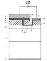
<Third Embodiment>
<Configuration>
FIG. 4 is a top view showing the configuration of the wide gap semiconductor device according to this embodiment, and FIG. 5 is a schematic cross-sectional view showing the configuration of the wide gap semiconductor device according to this embodiment.
本実施形態においては、内蔵する横型nチャネルMOSFETのソース電極がSiC−MOSFETの終端領域に形成されたグラウンド(以下、GNDと記載)配線9Bに接続された場合を示す。 In the present embodiment, the case where the source electrode of the built-in lateral n-channel MOSFET is connected to the ground (hereinafter referred to as GND) wiring 9B formed in the termination region of the SiC-MOSFET is shown.
図4に示されるように、複数のユニットセルが形成される活性領域を囲んで、ゲート配線32、GND配線9Bおよびフィールドリミッティングリング(以下、FLRと記載)33が形成されている。また、活性領域を覆うようにソースパッド30が配置され、ゲート配線32に沿ってゲートパッド31が配置されている。
As shown in FIG. 4, a
SiC−MOSFETに内蔵される横型nチャネルMOSFETは、活性領域と終端領域との境界に配置されている。 The lateral n-channel MOSFET built in the SiC-MOSFET is disposed at the boundary between the active region and the termination region.
図5は、図4におけるA−A’断面を示した図である。 FIG. 5 is a view showing a cross section taken along line A-A ′ in FIG. 4.
図5においては、横型nチャネルMOSFETのソース電極として、終端領域のGND配線9Bが用いられている。当該GND配線9Bおよび横型nチャネルMOSFETは、終端領域保護膜14に覆われている。
In FIG. 5, the GND wiring 9B in the termination region is used as the source electrode of the lateral n-channel MOSFET. The GND wiring 9B and the lateral n-channel MOSFET are covered with a termination
SiC−MOSFETのゲート電極とソース電極との間に過電圧が印加されたとき、内蔵されている横型nチャネルMOSFETのゲート電極とソース電極との間にも電圧が印加される。よって、横型nチャネルMOSFETにおいてnチャネルが形成される。 When an overvoltage is applied between the gate electrode and the source electrode of the SiC-MOSFET, a voltage is also applied between the gate electrode and the source electrode of the built-in lateral n-channel MOSFET. Therefore, an n channel is formed in the lateral n channel MOSFET.
横型nチャネルMOSFETにnチャネルが形成されるため、SiC−MOSFETのゲート電極とソース電極との間の過電圧によって発生するゲート電流は、横型nチャネルMOSFETの方に流れる(図5におけるX2を参照)。 Since the n-channel is formed in the lateral n-channel MOSFET, the gate current generated by the overvoltage between the gate electrode and the source electrode of the SiC-MOSFET flows toward the lateral n-channel MOSFET (see X2 in FIG. 5). .
内蔵する横型nチャネルMOSFETのソース電極を、SiC−MOSFETの終端領域のGND配線9Bとすることで、SiC−MOSFETの活性動作(ユニットセル動作)に影響することなく、ゲート電極とソース電極との間に過電圧が印加されたときに発生するゲート電流をGND配線に逃がすことができる。 By using the GND wiring 9B in the termination region of the SiC-MOSFET as the source electrode of the built-in lateral n-channel MOSFET, the gate electrode and the source electrode can be connected without affecting the active operation (unit cell operation) of the SiC-MOSFET. A gate current generated when an overvoltage is applied between them can be released to the GND wiring.
<効果>
本実施形態によれば、第2ソース電極が、縦型ワイドギャップ半導体MOSFETを囲んで形成された終端領域のグラウンド配線である。
<Effect>
According to this embodiment, the second source electrode is the ground wiring in the termination region formed so as to surround the vertical wide gap semiconductor MOSFET.
このような構成によれば、内蔵横型nチャネルMOSFETのソース電極をSiC−MOSFETの終端接合領域のグラウンド(GND)配線に接続することで、SiC−MOSFETの活性領域の動作に影響することなく、SiC−MOSFETのゲート電極とソース電極との間に過電圧が印加されることによるゲート電流をグラウンド(GND)配線へ逃がすことができる。 According to such a configuration, by connecting the source electrode of the built-in lateral n-channel MOSFET to the ground (GND) wiring of the termination junction region of the SiC-MOSFET, the operation of the active region of the SiC-MOSFET is not affected. A gate current caused by applying an overvoltage between the gate electrode and the source electrode of the SiC-MOSFET can be released to the ground (GND) wiring.
<第4実施形態>
<構成>
図6は、本実施形態に関するワイドギャップ半導体装置の構成を示す上面図であり、また図7は、本実施形態に関するワイドギャップ半導体装置の構成を示す断面概略図である。
<Fourth embodiment>
<Configuration>
FIG. 6 is a top view showing the configuration of the wide gap semiconductor device according to this embodiment, and FIG. 7 is a schematic cross-sectional view showing the configuration of the wide gap semiconductor device according to this embodiment.
本実施形態においては、内蔵する横型nチャネルMOSFETのソース電極がSiC−MOSFETのソース電極と同一層である場合を示す。 In this embodiment, the case where the source electrode of the built-in lateral n-channel MOSFET is the same layer as the source electrode of the SiC-MOSFET is shown.
図6に示されるように、複数のユニットセルが形成される活性領域を囲んで、ゲート配線32およびFLR33が形成されている。また、活性領域を覆うようにソースパッド30が配置され、ゲート配線32に沿ってゲートパッド31が配置されている。
As shown in FIG. 6,
SiC−MOSFETに内蔵される横型nチャネルMOSFETは、活性領域と終端領域との境界に配置されている。 The lateral n-channel MOSFET built in the SiC-MOSFET is disposed at the boundary between the active region and the termination region.
図7は、図6におけるA−A’断面を示した図である。 FIG. 7 is a view showing a cross section taken along line A-A ′ in FIG. 6.
図7においては、横型nチャネルMOSFETのソース電極は、SiC−MOSFETのソース電極9である。
In FIG. 7, the source electrode of the lateral n-channel MOSFET is the
そして、一方のn+ソース層4A(図5とは反対側)を覆って、ゲート電極12が形成されている。なお、上記のゲートポリシリコン7Bは、ゲート電極12が形成されている側のフィールド絶縁膜11側面にも形成されている。
A
また、層間絶縁膜8Aおよび他方のn+ソース層4Aを部分的に覆って、ソース電極9が形成されている。横型nチャネルMOSFETのゲートポリシリコン7Bは、層間絶縁膜8Aに覆われていない。また横型nチャネルMOSFETは、終端領域保護膜14に覆われている。
A
SiC−MOSFETのゲート電極とソース電極との間に過電圧が印加されたとき、内蔵されている横型nチャネルMOSFETのゲート電極とソース電極との間にも電圧が印加される。よって、横型nチャネルMOSFETにおいてnチャネルが形成される。 When an overvoltage is applied between the gate electrode and the source electrode of the SiC-MOSFET, a voltage is also applied between the gate electrode and the source electrode of the built-in lateral n-channel MOSFET. Therefore, an n channel is formed in the lateral n channel MOSFET.
横型nチャネルMOSFETにnチャネルが形成されるため、SiC−MOSFETのゲート電極とソース電極との間の過電圧によって発生するゲート電流は、横型nチャネルMOSFETの方に流れる(図7におけるX3を参照)。 Since the n-channel is formed in the lateral n-channel MOSFET, the gate current generated by the overvoltage between the gate electrode and the source electrode of the SiC-MOSFET flows toward the lateral n-channel MOSFET (see X3 in FIG. 7). .
<効果>
内蔵する横型nチャネルMOSFETのソース電極を、SiC−MOSFETのソース電極とすることで、横型nチャネルMOSFETのソース電極を新たに形成する必要がなくなり、SiC−MOSFETチップの無効領域の増加を抑えることができる。無効領域の増加を抑えることで、チップ面積を増やすことなく横型nチャネルMOSFETを内蔵でき、チップコストの増加を抑えることができる。
<Effect>
By using the source electrode of the built-in lateral n-channel MOSFET as the source electrode of the SiC-MOSFET, there is no need to newly form the source electrode of the lateral n-channel MOSFET, and the increase in the ineffective area of the SiC-MOSFET chip is suppressed. Can do. By suppressing the increase in the ineffective region, a lateral n-channel MOSFET can be built in without increasing the chip area, and an increase in chip cost can be suppressed.
<第5実施形態>
<構成>
図8は、本実施形態に関するワイドギャップ半導体装置の構成を示す上面図である。
<Fifth Embodiment>
<Configuration>
FIG. 8 is a top view showing the configuration of the wide gap semiconductor device according to this embodiment.
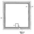
本実施形態においては、内蔵する横型nチャネルMOSFETが、SiC−MOSFETのゲート電極のワイヤボンディングパッド領域内に配置された場合を示す。 In the present embodiment, the case where the built-in lateral n-channel MOSFET is arranged in the wire bonding pad region of the gate electrode of the SiC-MOSFET is shown.
図8に示されるように、複数のユニットセルが形成される活性領域を囲んで、ゲート配線32およびFLR33が形成されている。また、活性領域を覆うようにソースパッド30が配置され、ゲート配線32に沿ってゲートパッド31が配置されている。
As shown in FIG. 8,
SiC−MOSFETに内蔵される横型nチャネルMOSFETは、活性領域と終端領域との境界に配置され、ゲートパッド31内に配置されている。
The lateral n-channel MOSFET built in the SiC-MOSFET is disposed at the boundary between the active region and the termination region, and is disposed in the
<効果>
このように、SiC−MOSFETのゲート電極のワイヤボンディングパッド領域内に配置することで、SiC−MOSFETチップの無効領域を増やすことなく横型nチャネルMOSFETを内蔵でき、チップコストの増加を抑えることができる。また、チップの無効面積の増加を防ぐことができる。
<Effect>
As described above, by arranging the SiC-MOSFET in the wire bonding pad region of the gate electrode of the SiC-MOSFET, it is possible to incorporate a lateral n-channel MOSFET without increasing the ineffective region of the SiC-MOSFET chip, and to suppress an increase in chip cost. . In addition, an increase in the ineffective area of the chip can be prevented.
<第6実施形態>
<構成>
図9に、電流センスMOSFETのゲート電極とソース電極との間に、横型のnチャネルMOSFETを内蔵させた、ワイドギャップ半導体装置の回路図を示す。なお、当該電流センスMOSFETは、SiC−MOSFETに内蔵されるMOSFETである。
<Sixth Embodiment>
<Configuration>
FIG. 9 shows a circuit diagram of a wide gap semiconductor device in which a lateral n-channel MOSFET is built between the gate electrode and the source electrode of the current sense MOSFET. The current sense MOSFET is a MOSFET built in the SiC-MOSFET.
電流センスは、Intelligent Power Module(以下、IPMと記載)等に使用されるIGBTチップ、MOSFETチップ等に内蔵されており、チップに過電流が流れたときの保護および検知に使用される。 The current sense is built in an IGBT chip, a MOSFET chip, or the like used in an intelligent power module (hereinafter referred to as IPM), and is used for protection and detection when an overcurrent flows through the chip.
一般的には、電流センスとなるMOSFETでは、IGBTチップまたはMOSFETチップ等の活性領域に流れる電流の1万分の1程度の電流を流すことができる活性領域の面積になっており、電流センスの活性領域面積は狭くゲート電極とソース電極との間の容量は小さいため、ゲート電極とソース電極との間の静電破壊耐量が低い。 In general, a MOSFET that serves as a current sense has an area of an active region in which about a tenth of a current that flows in an active region such as an IGBT chip or a MOSFET chip can flow. Since the area of the region is small and the capacitance between the gate electrode and the source electrode is small, the electrostatic breakdown resistance between the gate electrode and the source electrode is low.
図9に示されるように、電流センスMOSFETに、横型nチャネルMOSFETが内蔵されている。すなわち、電流センスMOSFETのゲート電極側に、横型nチャネルMOSFETのドレインおよびゲート電極が接続されている。 As shown in FIG. 9, a lateral n-channel MOSFET is built in the current sense MOSFET. That is, the drain and gate electrodes of the lateral n-channel MOSFET are connected to the gate electrode side of the current sense MOSFET.
<効果>
このように構成することで、電流センスMOSFETのゲート電極とソース電極との間に正の過電圧が印加されたときに、横型nチャネルMOSFET側に電流が流れることで、電流センスMOSFETのゲート電極とソース電極との間の静電破壊等の過電圧破壊を抑制することができる。また、チップの無効面積の増加を防ぐことができる。
<Effect>
With this configuration, when a positive overvoltage is applied between the gate electrode and the source electrode of the current sense MOSFET, a current flows to the lateral n-channel MOSFET side. Overvoltage breakdown such as electrostatic breakdown with the source electrode can be suppressed. In addition, an increase in the ineffective area of the chip can be prevented.
<第7実施形態>
<構成>
第6実施形態に示されたワイドギャップ半導体装置において、内蔵する横型nチャネルMOSFETのゲート電極とソース電極との間の閾値電圧(VGSth)を25V以上とすることで、横型nチャネルMOSFETが、電流センスMOSFETの通常の動作へ影響を与えることを防ぐことができる。
<Seventh embodiment>
<Configuration>
In the wide gap semiconductor device shown in the sixth embodiment, the threshold voltage (VGSth) between the gate electrode and the source electrode of the built-in lateral n-channel MOSFET is set to 25 V or more so that the lateral n-channel MOSFET This can prevent the normal operation of the sense MOSFET from being affected.
一般的な電流センスMOSFETのゲート電極とソース電極との間の最大定格電圧は20Vであるため、内蔵する横型nチャネルMOSFETのVGSthを25V以上とすることで、ゲート電極とソース電極との間電圧20V以下の通常の電流センスMOSFETの動作時には横型nチャネルMOSFETが動作しないためである。 Since the maximum rated voltage between the gate electrode and the source electrode of a general current sense MOSFET is 20 V, the voltage between the gate electrode and the source electrode can be increased by setting VGSth of the built-in lateral n-channel MOSFET to 25 V or more. This is because the lateral n-channel MOSFET does not operate during operation of a normal current sense MOSFET of 20 V or less.
なお、横型nチャネルMOSFETのVGSthを25V以上とすることで、横型nチャネルMOSFETの順方向電圧降下(オン電圧)も大きくなり、ゲート過電圧により発生したゲート電流は、横型nチャネルMOSFETで消費することができる。そのため、横型nチャネルMOSFETと電流センスMOSFETの間に、ゲート電流を消費する抵抗の付加が不要となる。 By setting VGSth of the lateral n-channel MOSFET to 25 V or more, the forward voltage drop (ON voltage) of the lateral n-channel MOSFET also increases, and the gate current generated by the gate overvoltage is consumed by the lateral n-channel MOSFET. Can do. Therefore, it is not necessary to add a resistor that consumes a gate current between the lateral n-channel MOSFET and the current sense MOSFET.
<第8実施形態>
<構成>
図10は、本実施形態に関するワイドギャップ半導体装置の構成を示す上面図である。
<Eighth Embodiment>
<Configuration>
FIG. 10 is a top view showing the configuration of the wide gap semiconductor device according to this embodiment.
本実施形態においては、内蔵する横型nチャネルMOSFETが、電流センスMOSFETのワイヤボンディングパッド領域内に配置された場合を示す。 In the present embodiment, a case where the built-in lateral n-channel MOSFET is arranged in the wire bonding pad region of the current sense MOSFET is shown.
図10に示されるように、複数のユニットセルが形成される活性領域を囲んで、ゲート配線32およびFLR33が形成されている。また、活性領域を覆うようにソースパッド30が配置され、ゲート配線32に沿ってゲートパッド31および電流センスパッド34が配置されている。
As shown in FIG. 10,
電流センスMOSFETに内蔵される横型nチャネルMOSFETは、電流センスパッド34内に配置されている。
A lateral n-channel MOSFET built in the current sense MOSFET is disposed in the
<効果>
このように、電流センスMOSFETのワイヤボンディングパッド領域内に配置することで、SiC−MOSFETチップの無効領域を増やすことなく横型nチャネルMOSFETを内蔵でき、チップコストの増加を抑えることができる。
<Effect>
As described above, by disposing in the wire bonding pad region of the current sense MOSFET, a lateral n-channel MOSFET can be built in without increasing the ineffective region of the SiC-MOSFET chip, and an increase in chip cost can be suppressed.
<第9実施形態>
<構成>
図11および図12は、第2実施形態および第7実施形態において、内蔵する横型nチャネルMOSFETのフィールド絶縁膜11が、SiC−MOSFETのフィールド酸化工程で同時に形成された場合を示す。
<Ninth Embodiment>
<Configuration>
11 and 12 show a case where the
一般的に、SiC−MOSFET周辺領域におけるフィールド酸化工程で形成される酸化膜は、活性領域(ユニットセル)におけるゲート酸化膜6よりも膜厚が厚い。フィールド酸化工程において形成される当該酸化膜を、横型nチャネルMOSFETのゲート絶縁膜として利用することで、工程を増やすことなく横型nチャネルMOSFETのゲート絶縁膜を形成することができる。また、当該酸化膜の膜厚が厚いことで、横型nチャネルMOSFETのVGSthをSiC−MOSFETのVGSthよりも高くすることができる。
Generally, the oxide film formed in the field oxidation process in the SiC-MOSFET peripheral region is thicker than the
そのため、チップコストを増加させることなく、SiC−MOSFETの通常の動作に影響しない横型nチャネルMOSFETを内蔵させることができる。 Therefore, a lateral n-channel MOSFET that does not affect the normal operation of the SiC-MOSFET can be incorporated without increasing the chip cost.
<効果>
本実施形態によれば、フィールド絶縁膜11が、縦型ワイドギャップ半導体MOSFETを囲む周辺領域の形成工程において形成されたものである。
<Effect>
According to this embodiment, the
一般的に、SiC−MOSFETのフィールド酸化工程で形成する酸化膜は、SiC−MOSFETの活性領域のゲート酸化膜より厚い。フィールド酸化工程の酸化膜を横型nチャネルMOSFETのゲート酸化膜に使用することで、工程を増やすことなく、横型nチャネルMOSFETのゲート電極とソース電極との間の閾値電圧を、SiC−MOSFETの活性領域のゲート電極とソース電極との間の閾値電圧より高くすることができる。 Generally, the oxide film formed in the field oxidation process of the SiC-MOSFET is thicker than the gate oxide film in the active region of the SiC-MOSFET. By using the oxide film of the field oxidation process as the gate oxide film of the lateral n-channel MOSFET, the threshold voltage between the gate electrode and the source electrode of the lateral n-channel MOSFET can be increased without increasing the number of processes. The threshold voltage between the gate electrode and the source electrode in the region can be higher.
<第10実施形態>
<構成>
本実施形態では、第2実施形態および第7実施形態において、ワイドギャップ半導体層表層をエッチングして凹部20を形成し、当該凹部20内に、横型nチャネルMOSFETのn+ソース層4Aを形成した場合を示す。
<Tenth Embodiment>
<Configuration>
In this embodiment, in the second embodiment and the seventh embodiment, when the
図13および図15は、本実施形態に関するワイドギャップ半導体装置の構成を示す断面概略図である。図14は、図13におけるA−A’の濃度プロファイルを示す図であり、図16は、図15におけるB−B’の濃度プロファイルを示す図である。図14および図16においては、縦軸に各層の不純物濃度が示され、横軸に、図13および図15における横方向をX軸とした場合のX軸方向の位置が示されている。 13 and 15 are schematic cross-sectional views showing the configuration of the wide gap semiconductor device according to this embodiment. 14 is a diagram showing the density profile of A-A ′ in FIG. 13, and FIG. 16 is a diagram showing the density profile of B-B ′ in FIG. 15. 14 and 16, the vertical axis indicates the impurity concentration of each layer, and the horizontal axis indicates the position in the X-axis direction when the horizontal direction in FIGS. 13 and 15 is the X-axis.
図14および図16に示されるように、一般的に、pベース層の濃度はn−層2表層から深い部分へ進むほどp型濃度が高くなる。よって、n−層2表層をエッチングして凹部20を形成し、凹部20内に横型nチャネルMOSFETのn+ソース層4Aを形成することにより、SiC−MOSFETの活性領域よりp型濃度が高い領域において、横型nチャネルMOSFETのnチャネルを形成することができる。
As shown in FIGS. 14 and 16, generally, the p-type concentration of the p base layer increases as it goes from the surface layer of the n −
そのため、横型nチャネルMOSFETにおいて、ゲート絶縁膜を厚くしなくとも、SiC−MOSFETの活性領域(ユニットセル)より高いVGSthを得ることができる。 Therefore, in the lateral n-channel MOSFET, VGSth higher than that of the active region (unit cell) of the SiC-MOSFET can be obtained without increasing the thickness of the gate insulating film.
従って、ゲート電極とソース電極との間の最大定格電圧20V以下の通常動作においても、SiC−MOSFETの通常の動作に影響しない横型nチャネルMOSFETを内蔵させることができる。 Accordingly, it is possible to incorporate a lateral n-channel MOSFET that does not affect the normal operation of the SiC-MOSFET even in a normal operation at a maximum rated voltage of 20 V or less between the gate electrode and the source electrode.
<効果>
本実施形態によれば、ワイドギャップ半導体装置が、pベース層3A(第2ベース層)表層に形成された凹部20を備える。そしてn+ソース層4Aが、凹部20内に形成されている。
<Effect>
According to this embodiment, the wide gap semiconductor device includes the
一般的に、SiC−MOSFETのpベース層濃度は、SiC最表面部より深い部分のp層濃度の方が高い。したがって、SiC表面をエッチングして凹部20を形成し、凹部20内にn+ソース層4Aが位置する横型nチャネルMOSFETを形成することにより、SiC−MOSFETの活性領域よりp層濃度が高い領域で、チャネルを形成することができる。
In general, the p-base layer concentration of the SiC-MOSFET is higher in the p-layer concentration in the portion deeper than the SiC outermost surface portion. Therefore, by etching the SiC surface to form the
そのため、横型nチャネルMOSFETのゲート酸化膜を厚くすることなく、SiC−MOSFETの活性領域より高いゲート電極とソース電極との間の閾値電圧を得ることができる。従って、ゲート電極とソース電極との間の最大定格電圧20V以下の通常動作では、横型nチャネルMOSFETが、SiC−MOSFETの活性領域、電流センスの動作に影響することはない。 Therefore, a threshold voltage between the gate electrode and the source electrode higher than the active region of the SiC-MOSFET can be obtained without increasing the thickness of the gate oxide film of the lateral n-channel MOSFET. Therefore, in a normal operation with a maximum rated voltage of 20 V or less between the gate electrode and the source electrode, the lateral n-channel MOSFET does not affect the operation of the active region and current sensing of the SiC-MOSFET.
上記実施形態では、各構成要素の材質、材料、実施の条件等についても記載しているが、これらは例示であって記載したものに限られるものではない。 In the said embodiment, although the material of each component, material, the conditions of implementation, etc. are described, these are illustrations and are not restricted to what was described.
なお本発明は、その発明の範囲内において、各実施形態の自由な組み合わせ、あるいは各実施形態の任意の構成要素の変形、もしくは各実施形態において任意の構成要素の省略が可能である。 In addition, within the scope of the present invention, the present invention can be freely combined with each embodiment, modified with any component in each embodiment, or omitted with any component in each embodiment.
1 バッファ層、2 n−層、3,3A pベース層、4,4A n+ソース層、5 p+層、6 ゲート酸化膜、7,7A,7B ゲートポリシリコン、8,8A 層間絶縁膜、9,9A ソース電極、9B GND配線、10 ドレイン電極、11 フィールド絶縁膜、12 ゲート電極、13,13A NiSi層、14 終端領域保護膜、20 凹部、30 ソースパッド、31 ゲートパッド、32 ゲート配線、33 FLR、34 電流センスパッド。 1 buffer layer, 2 n− layer, 3, 3A p base layer, 4, 4A n + source layer, 5 p + layer, 6 gate oxide film, 7, 7A, 7B gate polysilicon, 8, 8A interlayer insulating film, 9, 9A source electrode, 9B GND wiring, 10 drain electrode, 11 field insulating film, 12 gate electrode, 13, 13A NiSi layer, 14 termination region protective film, 20 recess, 30 source pad, 31 gate pad, 32 gate wiring, 33 FLR , 34 Current sense pad.
Claims (10)
前記第1ベース層表層に形成された、第1導電型の第1ソース層と、
前記第1ソース層と前記ワイドギャップ半導体層とに挟まれた前記第1ベース層上に形成されたゲート絶縁膜と、
前記ゲート絶縁膜上に形成された第1ゲート電極と、
前記第1ゲート電極を覆って形成された層間絶縁膜と、
前記層間絶縁膜、前記第1ベース層および前記第1ソース層を覆って形成された第1ソース電極と、
前記ワイドギャップ半導体層下に形成されたドレイン電極とを備える縦型ワイドギャップ半導体MOSFETと、
前記ワイドギャップ半導体層表層に、前記第1ベース層と同一工程で形成された第2ベース層と、
前記第2ベース層上に形成されたフィールド絶縁膜と、
前記第2ベース層表層において形成され、前記第2ベース層上に形成された前記フィールド絶縁膜を平面視において挟んで位置し、かつ、前記第1ソース層と同一工程で形成された第2ソース層と、
少なくとも前記フィールド絶縁膜上に形成された、前記第1ゲート電極と同一層である第2ゲート電極と、
一方の前記第2ソース層上に形成され、前記第2ゲート電極と電気的に接続された第3ゲート電極と、
他方の前記第2ソース層上に形成された第2ソース電極とを備える横型ワイドギャップ半導体MOSFETとを備え、
前記第1ゲート電極と前記第2ゲート電極とが電気的に接続され、
前記第1ソース電極と前記第2ソース電極とが電気的に接続されることを特徴とする、
ワイドギャップ半導体装置。 A first conductivity type first base layer formed on the surface layer of the first conductivity type wide gap semiconductor layer;
A first source layer of a first conductivity type formed on the surface layer of the first base layer;
A gate insulating film formed on the first base layer sandwiched between the first source layer and the wide gap semiconductor layer;
A first gate electrode formed on the gate insulating film;
An interlayer insulating film formed to cover the first gate electrode;
A first source electrode formed to cover the interlayer insulating film, the first base layer, and the first source layer;
A vertical wide gap semiconductor MOSFET comprising a drain electrode formed under the wide gap semiconductor layer;
A second base layer formed on the surface layer of the wide gap semiconductor layer in the same step as the first base layer;
A field insulating film formed on the second base layer;
A second source formed on the surface layer of the second base layer , located in a plan view with the field insulating film formed on the second base layer interposed therebetween, and formed in the same process as the first source layer Layers,
A second gate electrode formed on at least the field insulating film and in the same layer as the first gate electrode;
A third gate electrode formed on one of the second source layers and electrically connected to the second gate electrode;
And a lateral wide-gap semiconductor MOSFET and a second source electrode formed on the other of the second source layer,
The first gate electrode and the second gate electrode are electrically connected;
And the first source electrode and the second source electrode and said Rukoto are electrically connected,
Wide gap semiconductor device.
請求項1に記載のワイドギャップ半導体装置。 The second source electrode is the same layer as the first source electrode,
The wide gap semiconductor device according to claim 1.
請求項1に記載のワイドギャップ半導体装置。 The second source electrode is a ground wiring in a termination region formed surrounding the vertical wide gap semiconductor MOSFET,
The wide gap semiconductor device according to claim 1.
請求項1〜3のいずれかに記載のワイドギャップ半導体装置。 In the lateral wide gap semiconductor MOSFET, a threshold voltage between the second gate electrode and the second source electrode is 25 V or more,
The wide gap semiconductor device according to claim 1.
請求項1〜4のいずれかに記載のワイドギャップ半導体装置。 The field insulating film is formed in a step of forming a peripheral region surrounding the vertical wide gap semiconductor MOSFET,
The wide gap semiconductor device according to claim 1.
請求項1〜5のいずれかに記載のワイドギャップ半導体装置。 The vertical wide gap semiconductor MOSFET is a current sense MOSFET,
The wide gap semiconductor device according to claim 1.
請求項1〜6のいずれかに記載のワイドギャップ半導体装置。 The lateral wide gap semiconductor MOSFET is disposed in a gate pad region of the vertical wide gap semiconductor MOSFET,
The wide gap semiconductor device according to claim 1.
請求項6に記載のワイドギャップ半導体装置。 The lateral wide gap semiconductor MOSFET is disposed in a current sense pad region of the vertical wide gap semiconductor MOSFET,
The wide gap semiconductor device according to claim 6.
前記第2ソース層が、前記凹部内に形成されていることを特徴とする、
請求項1〜8のいずれかに記載のワイドギャップ半導体装置。 A concave portion formed on the surface layer of the second base layer;
The second source layer is formed in the recess,
The wide gap semiconductor device according to claim 1.
請求項1〜9のいずれかに記載のワイドギャップ半導体装置。 The wide gap semiconductor is SiC or GaN,
The wide gap semiconductor device according to claim 1.
Priority Applications (5)
| Application Number | Priority Date | Filing Date | Title |
|---|---|---|---|
| JP2013140348A JP6218462B2 (en) | 2013-07-04 | 2013-07-04 | Wide gap semiconductor device |
| US14/223,099 US9472543B2 (en) | 2013-07-04 | 2014-03-24 | Wide band gap semiconductor device |
| KR1020140074047A KR101596235B1 (en) | 2013-07-04 | 2014-06-18 | Wide band gap semiconductor device |
| DE102014211903.0A DE102014211903B4 (en) | 2013-07-04 | 2014-06-20 | Wide bandgap semiconductor device |
| CN201410320367.1A CN104282686B (en) | 2013-07-04 | 2014-07-04 | Wide band gap semiconductor device |
Applications Claiming Priority (1)
| Application Number | Priority Date | Filing Date | Title |
|---|---|---|---|
| JP2013140348A JP6218462B2 (en) | 2013-07-04 | 2013-07-04 | Wide gap semiconductor device |
Publications (3)
| Publication Number | Publication Date |
|---|---|
| JP2015015329A JP2015015329A (en) | 2015-01-22 |
| JP2015015329A5 JP2015015329A5 (en) | 2016-03-10 |
| JP6218462B2 true JP6218462B2 (en) | 2017-10-25 |
Family
ID=52106491
Family Applications (1)
| Application Number | Title | Priority Date | Filing Date |
|---|---|---|---|
| JP2013140348A Active JP6218462B2 (en) | 2013-07-04 | 2013-07-04 | Wide gap semiconductor device |
Country Status (5)
| Country | Link |
|---|---|
| US (1) | US9472543B2 (en) |
| JP (1) | JP6218462B2 (en) |
| KR (1) | KR101596235B1 (en) |
| CN (1) | CN104282686B (en) |
| DE (1) | DE102014211903B4 (en) |
Families Citing this family (8)
| Publication number | Priority date | Publication date | Assignee | Title |
|---|---|---|---|---|
| JP5968548B2 (en) * | 2013-09-17 | 2016-08-10 | 三菱電機株式会社 | Semiconductor device |
| DE102014116625B4 (en) * | 2014-11-13 | 2020-06-18 | Infineon Technologies Austria Ag | Vertical semiconductor device and method of manufacturing the same |
| DE112016005768B4 (en) * | 2015-12-18 | 2023-03-16 | Rohm Co., Ltd. | semiconductor device |
| WO2018008068A1 (en) * | 2016-07-04 | 2018-01-11 | 三菱電機株式会社 | Manufacturing method for semiconductor device |
| CN111295763B (en) | 2017-11-13 | 2023-12-29 | 新电元工业株式会社 | Wide band gap semiconductor device |
| JP7121547B2 (en) * | 2018-06-04 | 2022-08-18 | 株式会社豊田中央研究所 | semiconductor equipment |
| JP7145817B2 (en) * | 2019-06-14 | 2022-10-03 | 日立Astemo株式会社 | semiconductor equipment |
| CN117043961A (en) * | 2021-03-29 | 2023-11-10 | 三菱电机株式会社 | Semiconductor device, method for manufacturing semiconductor device, and method for replacing semiconductor device |
Family Cites Families (19)
| Publication number | Priority date | Publication date | Assignee | Title |
|---|---|---|---|---|
| JPS648674A (en) * | 1987-06-30 | 1989-01-12 | Rohm Co Ltd | Vertical mos-fet |
| JPH09119870A (en) * | 1995-10-26 | 1997-05-06 | Nec Corp | Temperature detection method, semiconductor device and temperature detection circuit |
| JPH09162399A (en) * | 1995-12-12 | 1997-06-20 | Toshiba Corp | Semiconductor device |
| US5602046A (en) * | 1996-04-12 | 1997-02-11 | National Semiconductor Corporation | Integrated zener diode protection structures and fabrication methods for DMOS power devices |
| JP3123930B2 (en) | 1996-08-20 | 2001-01-15 | 日本電気株式会社 | Semiconductor device |
| US6545316B1 (en) | 2000-06-23 | 2003-04-08 | Silicon Wireless Corporation | MOSFET devices having linear transfer characteristics when operating in velocity saturation mode and methods of forming and operating same |
| US7098506B2 (en) * | 2000-06-28 | 2006-08-29 | Renesas Technology Corp. | Semiconductor device and method for fabricating the same |
| JP2001274402A (en) * | 2000-03-24 | 2001-10-05 | Toshiba Corp | Power semiconductor device |
| US6465308B1 (en) * | 2001-05-24 | 2002-10-15 | Taiwan Semiconductor Manufacturing Company | Tunable threshold voltage of a thick field oxide ESD protection device with a N-field implant |
| JP3559971B2 (en) * | 2001-12-11 | 2004-09-02 | 日産自動車株式会社 | Silicon carbide semiconductor device and method of manufacturing the same |
| JP4770115B2 (en) | 2003-12-24 | 2011-09-14 | 住友電気工業株式会社 | Semiconductor device and manufacturing method of semiconductor device |
| JP4955222B2 (en) | 2005-05-20 | 2012-06-20 | ルネサスエレクトロニクス株式会社 | Manufacturing method of semiconductor device |
| JP4645705B2 (en) * | 2008-08-29 | 2011-03-09 | ソニー株式会社 | Semiconductor device and manufacturing method of semiconductor device |
| JP2012094555A (en) * | 2009-02-18 | 2012-05-17 | Mitsubishi Electric Corp | Method of manufacturing semiconductor device |
| JP5343904B2 (en) * | 2010-03-23 | 2013-11-13 | 住友電気工業株式会社 | Semiconductor device |
| JP2012054378A (en) | 2010-09-01 | 2012-03-15 | Renesas Electronics Corp | Semiconductor device |
| US8785931B2 (en) * | 2010-09-03 | 2014-07-22 | Mitsubishi Electric Corporation | Semiconductor device |
| JP5961865B2 (en) * | 2010-09-15 | 2016-08-02 | ローム株式会社 | Semiconductor element |
| CN102693981A (en) * | 2012-06-25 | 2012-09-26 | 吉林华微电子股份有限公司 | High-voltage VDMOS (Vertically Diffused Metal Oxide Semiconductor) tube taking LDMOS (Laterally Diffused Metal Oxide Semiconductor) as terminal |
-
2013
- 2013-07-04 JP JP2013140348A patent/JP6218462B2/en active Active
-
2014
- 2014-03-24 US US14/223,099 patent/US9472543B2/en active Active
- 2014-06-18 KR KR1020140074047A patent/KR101596235B1/en active IP Right Grant
- 2014-06-20 DE DE102014211903.0A patent/DE102014211903B4/en active Active
- 2014-07-04 CN CN201410320367.1A patent/CN104282686B/en active Active
Also Published As
| Publication number | Publication date |
|---|---|
| DE102014211903A1 (en) | 2015-01-08 |
| KR101596235B1 (en) | 2016-02-22 |
| US20150008450A1 (en) | 2015-01-08 |
| DE102014211903B4 (en) | 2017-08-10 |
| US9472543B2 (en) | 2016-10-18 |
| KR20150005443A (en) | 2015-01-14 |
| CN104282686A (en) | 2015-01-14 |
| JP2015015329A (en) | 2015-01-22 |
| CN104282686B (en) | 2017-05-17 |
Similar Documents
| Publication | Publication Date | Title |
|---|---|---|
| JP6218462B2 (en) | Wide gap semiconductor device | |
| JP6021032B2 (en) | Semiconductor device and manufacturing method thereof | |
| US10964686B2 (en) | Semiconductor device and method of manufacturing semiconductor device | |
| JP5757101B2 (en) | Super junction semiconductor device | |
| JP4772843B2 (en) | Semiconductor device and manufacturing method thereof | |
| JP5968548B2 (en) | Semiconductor device | |
| US9620595B2 (en) | Semiconductor device | |
| WO2017098547A1 (en) | Silicon carbide semiconductor device | |
| JP6526981B2 (en) | Semiconductor device and semiconductor module | |
| JP2009188178A (en) | Semiconductor device | |
| JP2009164460A (en) | Semiconductor device | |
| US9721939B2 (en) | Semiconductor device | |
| JP6338776B2 (en) | Semiconductor device | |
| TWI717713B (en) | Wide band gap semiconductor device | |
| JP2009099911A (en) | Semiconductor device | |
| JPH03180074A (en) | Semiconductor device | |
| KR20110081078A (en) | Semiconductor device | |
| JP4820899B2 (en) | Semiconductor device | |
| JP2009032968A (en) | Semiconductor device, and manufacturing method thereof | |
| JP2004014707A (en) | Semiconductor device | |
| JP2010199149A (en) | Semiconductor device | |
| JP2014103159A (en) | Semiconductor device | |
| JP2009088004A (en) | Semiconductor device | |
| JP2011108769A (en) | Semiconductor device |
Legal Events
| Date | Code | Title | Description |
|---|---|---|---|
| A521 | Request for written amendment filed |
Free format text: JAPANESE INTERMEDIATE CODE: A523 Effective date: 20160120 |
|
| A621 | Written request for application examination |
Free format text: JAPANESE INTERMEDIATE CODE: A621 Effective date: 20160120 |
|
| A977 | Report on retrieval |
Free format text: JAPANESE INTERMEDIATE CODE: A971007 Effective date: 20161222 |
|
| A131 | Notification of reasons for refusal |
Free format text: JAPANESE INTERMEDIATE CODE: A131 Effective date: 20170131 |
|
| A521 | Request for written amendment filed |
Free format text: JAPANESE INTERMEDIATE CODE: A523 Effective date: 20170309 |
|
| TRDD | Decision of grant or rejection written | ||
| A01 | Written decision to grant a patent or to grant a registration (utility model) |
Free format text: JAPANESE INTERMEDIATE CODE: A01 Effective date: 20170829 |
|
| A61 | First payment of annual fees (during grant procedure) |
Free format text: JAPANESE INTERMEDIATE CODE: A61 Effective date: 20170926 |
|
| R150 | Certificate of patent or registration of utility model |
Ref document number: 6218462 Country of ref document: JP Free format text: JAPANESE INTERMEDIATE CODE: R150 |
|
| R250 | Receipt of annual fees |
Free format text: JAPANESE INTERMEDIATE CODE: R250 |
|
| R250 | Receipt of annual fees |
Free format text: JAPANESE INTERMEDIATE CODE: R250 |
|
| R250 | Receipt of annual fees |
Free format text: JAPANESE INTERMEDIATE CODE: R250 |
|
| R250 | Receipt of annual fees |
Free format text: JAPANESE INTERMEDIATE CODE: R250 |