JP6211971B2 - Semiconductor test circuit and IC chip - Google Patents
Semiconductor test circuit and IC chip Download PDFInfo
- Publication number
- JP6211971B2 JP6211971B2 JP2014063880A JP2014063880A JP6211971B2 JP 6211971 B2 JP6211971 B2 JP 6211971B2 JP 2014063880 A JP2014063880 A JP 2014063880A JP 2014063880 A JP2014063880 A JP 2014063880A JP 6211971 B2 JP6211971 B2 JP 6211971B2
- Authority
- JP
- Japan
- Prior art keywords
- scan
- counter
- state
- signal
- data signal
- Prior art date
- Legal status (The legal status is an assumption and is not a legal conclusion. Google has not performed a legal analysis and makes no representation as to the accuracy of the status listed.)
- Active
Links
- 238000012360 testing method Methods 0.000 title claims description 70
- 239000004065 semiconductor Substances 0.000 title claims description 25
- 230000007704 transition Effects 0.000 claims description 25
- 238000010586 diagram Methods 0.000 description 24
- 230000000630 rising effect Effects 0.000 description 21
- 238000013461 design Methods 0.000 description 5
- 102100029469 WD repeat and HMG-box DNA-binding protein 1 Human genes 0.000 description 1
- 101710097421 WD repeat and HMG-box DNA-binding protein 1 Proteins 0.000 description 1
- 238000006243 chemical reaction Methods 0.000 description 1
- 238000007796 conventional method Methods 0.000 description 1
- 238000001514 detection method Methods 0.000 description 1
- 230000010354 integration Effects 0.000 description 1
- 238000000034 method Methods 0.000 description 1
- 238000012544 monitoring process Methods 0.000 description 1
Images


Landscapes
- Tests Of Electronic Circuits (AREA)
- Semiconductor Integrated Circuits (AREA)
Description
本発明は、半導体テスト回路及びICチップに関し、より詳細には、スキャンデータが入力されるSCANINとスキャンイネーブル信号が入力されるSCANENBを、同一ピンとした半導体テスト回路及びICチップに関する。 The present invention relates to a semiconductor test circuit and an IC chip, and more particularly to a semiconductor test circuit and an IC chip in which SCANIN to which scan data is input and SCANENB to which a scan enable signal is input have the same pin.
LSI(Large Scale Integration;大規模集積回路)のデジタルブロックは、一般に組み合わせ回路とFlip Flop(FF)による順序回路から構成されている。
図1は、一般的なLSI回路の例を示す回路構成図である。入力ピンDATAINと、出力ピンDATAOUTと、FFのリセット用ピンRSTと、FFのCLK用ピンSystemCLKをピンとして有している。FFA2a、FFB2b、FFC2cは、SystemCLKで動作するFFである。それぞれのFFの入力DA、DB、DCは、組み合わせ回路1の出力OA、OB、OCと接続し、FFの出力QA、QB、QCとDATAINピンは組み合わせ回路の入力INA、INB、INC、INDに接続されるように構成された回路である。
A digital block of an LSI (Large Scale Integration) is generally composed of a combinational circuit and a sequential circuit using a flip flop (FF).
FIG. 1 is a circuit configuration diagram showing an example of a general LSI circuit. An input pin DATAIN, an output pin DATAOUT, an FF reset pin RST, and an FF CLK pin SystemCLK are provided as pins. FF A 2a, FF B 2b, and FF C 2c are FFs that operate with SystemCLK. Input D A of the respective FF, D B, D C is the output O A of the combination circuit 1, O B, connected to the O C, the output Q A of FF, Q B, Q C and DATAIN pins combinational circuit A circuit configured to be connected to inputs IN A , IN B , IN C , and IN D.
一般に、LSIのテストは、回路中の全FFをMUX付きのFFに置き換え、そのMUXのセレクト信号により全FFをシフトレジスタ回路にする「SCAN動作」を出来るようにしている。これをSACN化という。
SCAN化された回路は、SCAN動作により、回路中の任意のノードに任意の値を設定できる制御と(control)、回路中の任意のノードの値を出力できる(observe)観測が自由となる。つまり、回路中の組み合わせ回路等に自由な値を設定し、その出力をモニタすることによって、故障検出率の高いテストを行うことができる。
In general, in the LSI test, all FFs in a circuit are replaced with FFs with MUXs, and a “SCAN operation” in which all FFs are made shift register circuits by the select signals of the MUXs. This is called SACN conversion.
The SCAN circuit can be controlled by an SCAN operation so that an arbitrary value can be set at an arbitrary node in the circuit (control), and the value of an arbitrary node in the circuit can be output (observe). That is, a test with a high failure detection rate can be performed by setting a free value to a combinational circuit in the circuit and monitoring its output.
このSCANテストを行うためには、例えば、以下の外部入力ピンを必要とする。
SCANIN:SCANデータの入力ピン
SCANENB:SCANパスと通常パスを切り替える入力ピン
SCANCLK:SCAN回路のCLK
SCANOUT:SCAN回路の出力ピン
SCANRST:SCAN回路のリセットピン
TESTMODE:SCANテストの許可ピン
In order to perform this SCAN test, for example, the following external input pins are required.
SCANIN: input pin for SCAN data SCANENB: input pin for switching between SCAN path and normal path SCANCLK: CLK of SCAN circuit
SCANOUT: SCAN circuit output pin SCANNRST: SCAN circuit reset pin TESTMODE: SCAN test enable pin
図2は、図1に示したSCAN化した回路構成図で、SCANテストを可能にした回路構成図である。入力ピンSCANINと、出力ピンSCANOUTと、FFのリセット用ピンSCANRSTと、FFの通常CLK用ピンSystemCLKと、FFのSCANテストCLK用ピンSCANCLKと、SCANパスと通常パスの切り替えピンSCANENBと、SCANテストの許可ピンTETSMODEをピンとして有している。組み合わせ回路1は、図1と同様である。
FIG. 2 is a circuit configuration diagram of the SCAN format shown in FIG. 1, and is a circuit configuration diagram that enables the SCAN test. Input pin SCANIN, output pin SCANOUT, FF reset pin SCANRST, FF normal CLK pin SystemCLK, FF SCAN test CLK pin SCANCLK, SCAN path / normal path switching pin SCANENB, SCAN test The permission pin TETSMODE is provided as a pin. The
全FFは、図1からMUX付のFFに変わり、そのセレクタ信号はSCANENBとTETSMODEのAND出力となる。このAND1はTESTMODEが0のとき、つまり、SCANテストモードではないときに、FFの入力が誤選択されないように保護するためである。以下、TESTMODEが1のときを考えると、FFのセレクタは、SCANENBが0のときは、図1と同様のパスとなり、SCANENBが1のときは、全FFがSCANINからSCANOUTまでのシフトレジスタとして動作する。 All FFs are changed from FIG. 1 to FFs with MUX, and the selector signal is an AND output of SCANENB and TETSMODE. This AND1 is for protecting the FF input from being erroneously selected when TESTMODE is 0, that is, when not in the SCAN test mode. In the following, when TESTMODE is 1, the FF selectors have the same path as in FIG. 1 when SCANENB is 0, and all FFs operate as shift registers from SCANIN to SCANOUT when SCANENB is 1. To do.
図3は、図2に示した回路における一般的なSCANテスト動作について説明するためのタイミングチャートを示す図である。前提としてTESTMODEは1とする。
(1);SCANENBを1にして全FFをSCAN動作可能にする。
(2);全FFに所望の値をSCAN動作によりセットする(図3ではFFA、;FFB、FFBにそれぞれDA1、DB1、DC1をセットしている)。
(3);SCANENBを0にして通常パスに戻す。
(4);SCANCLKから1CLK入力し、通常パスの出力(=組み合わせ回路の出力)を各FFに取り込む(図3ではFFA、FFB、FFBにそれぞれ組み合わせ回路出力のOA1、OB1、OC1が取り込まれる)。
(5);SCANENBを1にして全FFをSCAN動作可能にする。
(6);SCANCLKを入力して全FFの値(OA1、OB1、OC1)をSCANOUTから出力しモニタする(この際同時に全FFに次の所望の値DA2、DB2、DC2をセットする)。
(7);上記(3)〜(6)を繰り返す。
以上が一般的なスキャン化した回路のテスト動作である。
FIG. 3 is a timing chart for explaining a general SCAN test operation in the circuit shown in FIG. As a premise, TESTMODE is 1.
(1): Set SCANENB to 1 to enable all FFs to perform SCAN operation.
(2): Desired values are set to all FFs by SCAN operation (in FIG. 3, FF A , FF B , FF B are set to D A1 , D B1 , DC 1 respectively).
(3): Set SCANENB to 0 and return to the normal path.
(4); 1 CLK is input from SCANCLK, and the output of the normal path (= the output of the combinational circuit) is taken into each FF (in FIG. 3, FF A , FF B , and FF B are combined circuit outputs O A1 , O B1 , OC1 is incorporated).
(5): Set SCANENB to 1 to enable all FFs to perform SCAN operation.
(6); SCANCLK is input and the values (O A1 , O B1 , O C1 ) of all FFs are output from SCANOUT and monitored (at this time, the next desired values D A2 , D B2 , D C2 Set).
(7); (3) to (6) are repeated.
The above is a general scan operation of the circuit.
例えば、特許文献1では、ピン数の少ないLSIでもSCANテストを可能にするために、SCANINとSCANENBを共通化する方法を提案している。
図4は、特許文献1に記載されているSCANテストを可能にした回路構成図である。以下のような特徴を有している。
SCAN回路はSCANCLKの正転信号をCLKとする。
SCANINをデータ、SCANCLKの反転信号をCLK入力としたFFであるFFENB3の出力をSCANENBとする。
For example,
FIG. 4 is a circuit configuration diagram that enables the SCAN test described in
The SCAN circuit sets the normal signal of SCANCLK to CLK.
The output of
図5は、図4に示したSCANテスト動作を説明するためのタイミングチャートを示す図である。前提としてTESTMODEは1とする。
(1);SCANCLKが1のときにSCANINを1にする。
(2);SCANCLKの立ち下がりEdgeでSCANINからSCANENB用FFであるFFENBに1を取り込むことでSCAN動作を可能にする。
(3);SCANCLKが0のときにSCANINを所望の値にする。
(4);SCANCLKの立ち上がりEdgeでSCANINからSCAN化されたFFAに所望の値を取り込む(図5ではFFAにDC1をセットしている)。
(5);SCANCLKが1のときにSCANINを1にする。
FIG. 5 is a timing chart for explaining the SCAN test operation shown in FIG. As a premise, TESTMODE is 1.
(1): When SCANCLK is 1, SCANIN is set to 1.
(2): SCAN operation is enabled by taking 1 from SCANIN to FF ENB , which is a FF for SCANENB, at the falling edge of SCANCLK.
(3): When SCANCLK is 0, SCANIN is set to a desired value.
(4): A desired value is taken into SCANIN to FF A at the rising edge of SCANCLK (in FIG. 5, DC 1 is set to FF A ).
(5): When SCANCLK is 1, SCANIN is set to 1.
(6);SCANCLKの立ち下がりEdgeでSCANINからSCANENB用FFであるFFENBに1を取り込むことで引き続きSCAN動作を可能にする。
(7);上記(3)〜(6)を繰り返し全FFに所望の値をセットする(図5ではFFA、FFB、FFBにそれぞれDA1、DB1、DC1をセットしている)。
(8);SCANCLKが1のときにSCANINを0にする。
(9);SCANCLKの立ち下がりEdgeでSCANINからSCANENB用FFであるFFENBに0を取り込むことで通常パスに戻す。
(10)SCANCLKの立ち上がりEdgeで、通常パスの出力(=組み合わせ回路の出力)を各FFに取り込む(図5ではFFA、FFB、FFBにそれぞれ組み合わせ回路出力のOA1、OB1、OC1が取り込まれる)。
(6); SCAN operation is continuously enabled by fetching 1 from SCANIN to FF ENB , which is the FF for SCANENB, at the falling edge of SCANCLK.
(7); Repeat (3) to (6) above to set desired values in all FFs (in FIG. 5, D A1 , D B1 and D C1 are set in FF A , FF B and FF B , respectively) ).
(8): When SCANCLK is 1, SCANIN is set to 0.
(9): At the falling edge of SCANCLK, 0 is taken from SCANIN to FF ENB , which is the FF for SCANENB, to return to the normal path.
(10) At the rising edge of SCANCLK, the normal path output (= combined circuit output) is taken into each FF (in FIG. 5, FF A , FF B , and FF B are combined circuit outputs O A1 , O B1 , O respectively). C1 is taken in).
(11);SCANCLKが1のときにSCANINを1にする。
(12);SCANCLKの立ち下がりEdgeでSCANINからSCANENB用FFであるFFENBに1を取り込むことでSCAN動作を可能にする。
(13);SCANCLKを入力して全FFの値(OA1、OB1、OC1)をSCANOUTから出力しモニタする(この際同時に全FFに次の所望の値DA2、DB2、DC2をセットする。SCANENBは1のままになるようにしておく)。
(14);上記(8)〜(12)を繰り返す。
(11): When SCANCLK is 1, SCANIN is set to 1.
(12): SCAN operation is enabled by taking 1 from SCANIN to FF ENB which is the FF for SCANENB at the falling edge of SCANCLK.
(13); SCANCLK is input and the values (O A1 , O B1 , O C1 ) of all FFs are output from SCANOUT and monitored (at this time, the next desired values D A2 , D B2 , D C2 Set SCANENB to 1).
(14); (8) to (12) are repeated.
上述した特許文献1により、SCANINとSCANENBを共用してSCANテストが可能になる。しかし、通常のSCANテストでは、SCAN回路は、SCANCLKの立ち上がりと立下りEdgeで動作するFFが混在してもよいが、上述した従来の手法では、SCANENBは、SCANCLKの立下りEdgeで生成するため、SCAN回路は、必ずSCANCLKの立ち上がりEdgeで動作する必要があり、設計の自由度がない。また、立ち上がりEdge(SCAN用)と立下りEdge(SCANENB用)のFFが混在しているため、それぞれのFFのセットアップタイムとホールドタイムを確保する必要があり、SCANCLK周波数を挙げることができず、テスト時間の短縮ができない。
本発明は、このような問題に鑑みてなされたもので、その目的とするところは、設計の自由度が高く、また、テスト時間が短い半導体テスト回路及びICチップを提供することにある。
According to
The present invention has been made in view of such problems, and an object of the present invention is to provide a semiconductor test circuit and an IC chip having a high degree of design freedom and a short test time.
本発明は、このような目的を達成するためになされたもので、請求項1に記載の発明は、デジタル回路の故障検知を行うテストモードを有する半導体テスト回路において、スキャンイネーブル信号に基づいて、通常動作とスキャンデータ信号が入力されるシフトレジスタを構成するスキャン動作とを選択する選択回路を有する複数のフリップフロップ(12a〜12c)と、前記スキャンデータ信号が入力されて前記複数のフリップフロップへ出力する組み合わせ回路(11)と、前記スキャンデータ信号が入力されて前記スキャンイネーブル信号を出力するカウンタ(13)と、を備えることを特徴とする。
The present invention was made to achieve such an object, and the invention according to
また、請求項2に記載の発明は、請求項1に記載の発明において、前記スキャンデータ信号は、前記複数のフリップフロップがスキャンクロックに同期して取り込むデータ信号と、前記複数のフリップフロップに入力されるスキャンクロックが配されない区間に配されるカウンタ制御信号と、を有し、前記カウンタにおいて、前記カウンタ制御信号により、前記スキャンイネーブル信号が制御されることを特徴とする。
また、請求項3に記載の発明は、請求項1又は2に記載の発明において、前記スキャンデータ信号は、前記複数のフリップフロップがスキャンクロックに同期して取り込むデータ信号と、前記複数のフリップフロップに入力されるスキャンクロックが配されない区間に配されるカウンタ制御信号と、を有し、前記カウンタにおいて、前記カウンタ制御信号により、前記スキャンイネーブル信号が立ち上がる又は立ち下がることを特徴とする。
According to a second aspect of the invention, in the first aspect of the invention, the scan data signal is input to the plurality of flip-flops and a data signal that the plurality of flip-flops capture in synchronization with a scan clock. And a counter control signal arranged in a section where no scan clock is arranged, wherein the scan enable signal is controlled by the counter control signal in the counter.
According to a third aspect of the present invention, in the first or second aspect of the invention, the scan data signal includes a data signal captured by the plurality of flip-flops in synchronization with a scan clock, and the plurality of flip-flops. And a counter control signal arranged in a section where the scan clock inputted to the digital camera is not arranged. In the counter, the scan enable signal rises or falls according to the counter control signal.
また、請求項4に記載の発明は、請求項2又は3に記載の発明において、前記カウンタは、前記スキャンデータ信号と前記スキャンクロック信号が入力され、状態遷移するカウンタであることを特徴とする。
また、請求項5に記載の発明は、請求項4に記載の発明において、前記カウンタは、少なくとも4つの状態を遷移し、前記データ信号と前記スキャンクロック信号により、第1の状態と第2の状態の遷移を繰り返し、また、第3の状態と第4の状態の遷移を繰り返し、前記カウンタ制御信号により、前記第1の状態又は前記第2の状態から、前記第3の状態又は第4の状態への遷移、または、前記第3の状態又は前記第4の状態から、前記第1の状態又は第2の状態への遷移を行い、前記第1の状態又は前記第2の状態に対応するカウント値が通常動作に対応する前記イネーブル信号であり、前記第3の状態又は前記第4の状態に対応するカウント値がスキャン動作に対応する前記イネーブル信号であることを特徴とする。
The invention according to
According to a fifth aspect of the invention, in the invention of the fourth aspect, the counter transits at least four states, and the first state and the second state are changed by the data signal and the scan clock signal. The state transition is repeated, the transition between the third state and the fourth state is repeated, and the third state or the fourth state is changed from the first state or the second state by the counter control signal. A transition to a state, or a transition from the third state or the fourth state to the first state or the second state, corresponding to the first state or the second state The count value is the enable signal corresponding to the normal operation, and the count value corresponding to the third state or the fourth state is the enable signal corresponding to the scan operation.
また、請求項6に記載の発明は、請求項5に記載の発明において、前記カウンタは、前記スキャンクロック信号により、第1の状態又は第2の状態から第1の状態へリセットする遷移を行い、及び、第3の状態又は第4の状態から第3の状態へリセットする遷移を行うことを特徴とする。
また、請求項7に記載の発明は、請求項1〜6のいずれか一項に記載の発明において、前記カウンタは、2bitバイナリカウンタであり、前記スキャンイネーブル信号は、前記カウンタのカウント値のMSB又はLSBであることを特徴とする。
According to a sixth aspect of the present invention, in the fifth aspect of the present invention, the counter performs a transition to reset from the first state or the second state to the first state by the scan clock signal. And a transition to reset from the third state or the fourth state to the third state is performed.
The invention according to
また、請求項8に記載の発明は、複数のフリップフロップと組み合わせ回路とを有するデジタルブロックを、スキャンクロックと、スキャンデータ信号と、スキャンイネーブル信号と、によりスキャンテストを行うICチップであって、スキャンクロックが入力される第1のPAD(SCANCLK)と、スキャンデータ信号が入力される第2のPAD(SCANIN)と、前記第2のPADに接続され、前記スキャンデータ信号から前記スキャンイネーブル信号を出力するカウンタと、を備えることを特徴とする。
The invention according to
また、請求項9に記載の発明は、請求項8に記載の発明において、前記カウンタのクロックラインに、前記第2のPADが接続され、前記カウンタの第1のリセットラインに、前記第1のPADが論理素子を介して接続されることを特徴とする。
また、請求項10に記載の発明は、請求項8又は9に記載の発明において、前記スキャンデータ信号は、前記複数のフリップフロップがスキャンクロックに同期して取り込むデータ信号と、前記複数のフリップフロップに入力されるスキャンクロックが配されない区間に配されるパルス信号と、を有することを特徴とする。
The invention according to
The invention according to
また、請求項11に記載の発明は、請求項10に記載の発明において、前記データ信号を前記複数のフリップフロップに、前記スキャンクロックに同期して設定するために順次データが入力された後、次にスキャンクロックが配されるまでの間に、前記パルス信号が配されることを特徴とする。
また、請求項12に記載の発明は、請求項11に記載の発明において、前記次のスキャンクロックが配された後、別のデータ信号を前記複数のフリップフロップに、前記スキャンクロックに同期して設定するために順次データが入力されるまでの間に、前記パルス信号が配されることを特徴とする。
The invention according to
According to a twelfth aspect of the present invention, in the invention of the eleventh aspect, after the next scan clock is arranged, another data signal is sent to the plurality of flip-flops in synchronization with the scan clock. The pulse signal is arranged until data is sequentially input for setting.
本発明によれば、ピン数を削減したうえで、設計の自由度が高く、また、テスト時間が短い半導体テスト回路及びICチップを実現することができる。 According to the present invention, it is possible to realize a semiconductor test circuit and an IC chip having a high degree of design freedom and a short test time after reducing the number of pins.
以下、図面を参照して本発明の実施の形態について説明する。
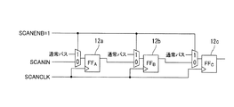
図6は、本発明に係るシフトレジスタ回路の回路構成図で、図7は、図6に示したシフトレジスタ回路の動作を説明するためのタイミングチャートを示す図である。図中符号12a,12b,12cは第1乃至第3のフリップフロップ(FFA、FFB、FFC)を示している。
本実施形態の半導体テスト回路は、SCANINをCLKとするカウンタを用いて、そのカウンタ値をSCANENBとすることにより、SCANINとSCANENBを同一ピンで制御できるため、ピン数の削減ができることを特徴とする。また、カウンタを用いることで、設計の自由度が高く、また、テスト時間が短いテストが可能となる。
Embodiments of the present invention will be described below with reference to the drawings.
6 is a circuit configuration diagram of the shift register circuit according to the present invention, and FIG. 7 is a timing chart for explaining the operation of the shift register circuit shown in FIG.
The semiconductor test circuit of the present embodiment is characterized in that the number of pins can be reduced because SCANIN and SCANENB can be controlled by the same pin by using a counter having SCANIN as CLK and the counter value being SCANENB. . Further, by using the counter, it is possible to perform a test with a high degree of design freedom and a short test time.
[実施形態]
本実施形態は、SCANINとSCANENBを共用するために、SCANENBをSCANCLKではなくSCANINをCLKとしたカウンタの値とすることを特徴とする。
以下に、基本原理について説明する。
SCAN動作は、SCANCLKのEdgeでSCANINを取り込みシフトレジスタ動作する。図6及び図7に示すように、SCANCLKのEdge以外では、SCANINは、どのように変化してもFFに取り込む値は変わらない。よって、SCANCLKのEdgeの前にSCANINにパルスを発生させ、そのSCANINをCLKとするカウンタを用意し、そのカウンタ値をもってSCANENBを生成する。
[Embodiment]
The present embodiment is characterized in that SCANINB is not a SCANCLK but a counter value having SCANIN as CLK in order to share SCANIN and SCANENB.
Hereinafter, the basic principle will be described.
In the SCAN operation, SCANIN is fetched at the edge of SCANCLK and the shift register operates. As shown in FIGS. 6 and 7, except for the edge of SCANCLK, the value taken into the FF does not change no matter how SCANIN changes. Therefore, a pulse is generated in SCANIN before Edge of SCANCLK, a counter having SCANIN as CLK is prepared, and SCANENB is generated with the counter value.
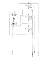
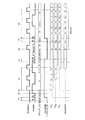
図8は、本発明に係る半導体テスト回路の実施例1を説明するための回路構成図で、SCANINとSCANENBとを共通化したSCANテストを可能にした回路構成図である。図中符号11は組み合わせ回路、13はカウンタを示している。なお、図6と同じ機能を有する構成要素には同一に符号を付してある。
本発明の半導体テスト回路は、デジタル回路の故障検知を行うテストモードを有する半導体テスト回路である。
複数のフリップフロップ12a〜12cは、スキャンイネーブル信号に基づいて、通常動作とスキャンデータ信号が入力されるシフトレジスタを構成するスキャン動作とを選択する選択回路を有する。
FIG. 8 is a circuit configuration diagram for explaining the first embodiment of the semiconductor test circuit according to the present invention, and is a circuit configuration diagram enabling a SCAN test in which SCANIN and SCANENB are shared. In the figure,
The semiconductor test circuit of the present invention is a semiconductor test circuit having a test mode for detecting a failure of a digital circuit.
Each of the plurality of flip-
組み合わせ回路11は、スキャンデータ信号が入力されて複数のフリップフロップへ出力する。カウンタ13は、スキャンデータ信号が入力されてスキャンイネーブル信号を出力する。
また、スキャンデータ信号は、複数のフリップフロップがスキャンクロックに同期して取り込むデータ信号と、複数のフリップフロップに入力されるスキャンクロックが配されない区間に配されるカウンタ制御信号と、を有し、カウンタにおいて、カウンタ制御信号により、スキャンイネーブル信号が制御される。
The
Further, the scan data signal has a data signal that the plurality of flip-flops capture in synchronization with the scan clock, and a counter control signal that is disposed in a section where the scan clock input to the plurality of flip-flops is not disposed, In the counter, the scan enable signal is controlled by the counter control signal.
また、スキャンデータ信号は、複数のフリップフロップがスキャンクロックに同期して取り込むデータ信号と、複数のフリップフロップに入力されるスキャンクロックが配されない区間に配されるカウンタ制御信号と、を有し、カウンタにおいて、カウンタ制御信号により、スキャンイネーブル信号が立ち上がる又は立ち下がる。
また、カウンタ13は、スキャンデータ信号とスキャンクロック信号が入力され、状態遷移するカウンタである。
また、カウンタ13は、少なくとも4つの状態を遷移し、データ信号とスキャンクロック信号により、第1の状態と第2の状態の遷移を繰り返し、また、第3の状態と第4の状態の遷移を繰り返し、カウンタ制御信号により、第1の状態又は第2の状態から、第3の状態又は第4の状態への遷移、または、第3の状態又は第4の状態から、第1の状態又は第2の状態への遷移を行い、第1の状態又は第2の状態に対応するカウント値が通常動作に対応するイネーブル信号であり、第3の状態又は第4の状態に対応するカウント値がスキャン動作に対応するイネーブル信号である。
Further, the scan data signal has a data signal that the plurality of flip-flops capture in synchronization with the scan clock, and a counter control signal that is disposed in a section where the scan clock input to the plurality of flip-flops is not disposed, In the counter, the scan enable signal rises or falls according to the counter control signal.
The
The
また、カウンタ13は、スキャンクロック信号により、第1の状態又は第2の状態から第1の状態へリセットする遷移を行い、及び、第3の状態又は第4の状態から第3の状態へリセットする遷移を行う。
また、カウンタ13は、2bitバイナリカウンタであり、スキャンイネーブル信号は、カウンタのカウント値のMSB(最上位ビット)である。なお、LSB(最下位ビット)をスキャンイネーブル信号とする構成であってもよい。
SCAN回路が、SCANCLKの立ち上がりEdgeで動作するときの新回路の例を図8に示している。SCANENBを、SCANINをCLKとしたカウンタの出力とするように構成する。
Further, the
The
An example of a new circuit when the SCAN circuit operates at the rising edge of SCANCLK is shown in FIG. SCANENB is configured to be the output of a counter with SCANIN set to CLK.
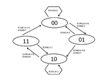
図9は、図8に示したカウンタの状態遷移図である。SCANCLKが0のとき、SCANINの立ち上がりEdgeで2進数表記で00⇒01⇒10⇒11⇒00⇒…と動作する2bitバイナリカウンタであり、そのMSBをSCANENBとして構成する。つまり、カウンタが2進数表記で00,01の時は、SCANENBが0に、カウンタが2進数表記で10,11のときは、SCANENBが1となる。また、SCANCLKが1のときは、カウンタのLSBが0になるようにリセットさせる。
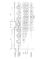
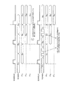
図10は、図8に示したSCANテスト動作を説明するためのタイミングチャートを示す図である。
FIG. 9 is a state transition diagram of the counter shown in FIG. When SCANCLK is 0, this is a 2-bit binary counter that operates in binary notation at the rising edge of SCANIN in the form of 00⇒01⇒10⇒11⇒00⇒ ..., and its MSB is configured as SCANENB. That is, when the counter is 00 and 01 in binary notation, SCANENB is 0, and when the counter is 10 and 11 in binary notation, SCANENB is 1. When SCANCLK is 1, the counter is reset so that LSB becomes 0.
FIG. 10 is a timing chart for explaining the SCAN test operation shown in FIG.
(1);SCANCLKが0のときにSCANINから2発パルスを入れることでカウンタを2進数表記で00⇒01⇒10とし、SCANENBを1にして全FFをSCAN動作可能にする。
(2);SCANCLKが0のときにSCANINを所望の0または1にする(図9では1にセットしている。この際カウンタは2進数表記で11となる)。
(3);SCANCLKを入れてFFAに所望の値を取り込む(図9では1をとりこむ。このときカウンタはSCANCLKが1のためLSBがリセットされ必ず2進数表記で10になる)。
(1): By inputting two pulses from SCANIN when SCANCLK is 0, the counter is changed to 00⇒01⇒10 in binary notation, and SCANENB is set to 1 to enable all FFs to perform SCAN operation.
(2): When SCANCLK is 0, SCANIN is set to a desired 0 or 1 (in FIG. 9, it is set to 1. In this case, the counter is 11 in binary notation).
(3); Put SCANCLK incorporate desired value FF A (. Fetches a 9 this time counter SCANCLK becomes 10 LSB is always reset the binary notation for 1).
(4);(2),(3)を繰り返し全FFに所望の値をセットする(図9ではFFA、FFB、FFBにそれぞれ1、0、1をセットしている)。
(5);SCANCLKが0のときにSCANINから2発パルスを入れることでカウンタを2進数表記で10⇒11⇒00とし、SCANENBを0(=通常パス)にする。
(6);SCANCLKから1CLK入力し、通常パスの出力(=組み合わせ回路の出力)を各FFに取り込む(図10ではFFA、FFB、FFBにそれぞれ組み合わせ回路出力のQA1、QB1、QC1が取り込まれる。このときカウンタはSCANCLKが1のためLSBがリセットされ必ず2進数表記で00になる)。
(4); (2) and (3) are repeated and desired values are set in all FFs (in FIG. 9, FF A , FF B , and FF B are set to 1, 0, 1 respectively).
(5): By inputting two pulses from SCANIN when SCANCLK is 0, the counter is changed from 10⇒11⇒00 in binary notation, and SCANENB is set to 0 (= normal path).
(6); 1 CLK is input from SCANCLK, and the output of the normal path (= the output of the combinational circuit) is taken into each FF (in FIG. 10, FF A , FF B , and FF B are combined circuit outputs Q A1 , Q B1 , Q C1 is captured. the time counter becomes 00 SCANCLK is in LSB is always reset the binary notation for 1).
(7);SCANCLKが0のときにSCANINから2発パルスを入れることでカウンタを2進数表記で00⇒01⇒10とし、SCANENBを1にして全FFをSCAN動作可能にする。
(8);SCANCLKを入力して全FFの値(QA1、QB1、QC1)をSCANOUTから出力しモニタする(この際同時に全FFに次の所望の値をセットする。図10では0、1、0をそれぞれセットしている)。
(9);上記(5)〜(8)を繰り返す。
(7): By inputting two pulses from SCANIN when SCANCLK is 0, the counter is changed from 00⇒01⇒10 in binary notation, and SCANENB is set to 1 to enable all FFs to perform SCAN operation.
(8): SCANCLK is input, and the values of all FFs (Q A1 , Q B1 , Q C1 ) are output from SCANOUT and monitored (at this time, the next desired value is set to all FFs simultaneously. In FIG. 10, 0) 1 and 0 are set respectively).
(9); The above (5) to (8) are repeated.
本実施例1におけるカウンタは、2bitのバイナリカウンタとしたが、カウンタは、2bit以上であればbit数は問わない。また、本実施例1は、バイナリカウンタとしたがカウンタの種類は問わない。また、本実施例1は、カウンタの動作は、SCANINのEdgeは立ち上がりとしたがEdgeの向きは問わない。また、SCANENBが0又は1となるカウンタ値もSCAN動作と通常パスが切り替えることができるように自由に決めてよい。カウンタのリセット信号は、本実施例1では、SCANテストを行う際に1とするTESTMODE信号の反転信号をリセットとしたが、通常動作時にSCANENBが1にならないようにすれば構成は問わない。
更に、本実施例1は、カウンタのLSBのリセット信号にSCANCLKの1を入力しているが、これはSCANCLKが1となるとカウンタが2進数表記で00又は10となり、カウンタの値を把握しやすくするためのものであり、取り除いても構わない。その場合の構成例を以下の実施例2に示す。
Although the counter in the first embodiment is a 2-bit binary counter, the number of bits is not limited as long as the counter is 2 bits or more. In the first embodiment, a binary counter is used, but the type of the counter is not limited. In the first embodiment, the counter operation is such that the edge of SCANIN rises, but the direction of Edge does not matter. Also, the counter value at which SCANENB becomes 0 or 1 may be freely determined so that the SCAN operation and the normal path can be switched. In the first embodiment, the counter reset signal is reset when the inverted signal of the TESTMODE signal is set to 1 when the SCAN test is performed. However, the configuration is not limited as long as SCANENB does not become 1 during normal operation.
Furthermore, in the first embodiment,
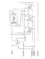
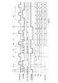
図11は、本発明に係る半導体テスト回路の実施例2を説明するための回路構成図で、SCANINとSCANENBとを共通化したSCANテストを可能にした回路構成図である。なお、図8と同じ機能を有する構成要素には同一に符号を付してある。
SCAN回路がSCANCLKの立ち上がりEdgeで動作するときの新回路の例を図11に示してある。SCANENBを、SCANINをCLKとしたカウンタ13の出力とするように構成する。カウンタ13は、SCANテストを行うTESTMODE=1以外はリセットされる。
FIG. 11 is a circuit configuration diagram for explaining the semiconductor test circuit according to the second embodiment of the present invention, and is a circuit configuration diagram enabling SCAN test in which SCANIN and SCANENB are shared. Components having the same functions as those in FIG. 8 are denoted by the same reference numerals.
FIG. 11 shows an example of a new circuit when the SCAN circuit operates at the rising edge of SCANCLK. SCANENB is configured to be the output of the
図12は、図11に示したカウンタの状態遷移図である。SCANCLKが0のとき、SCANINの立ち上がりEdgeで2進数表記で00⇒01⇒10⇒11⇒00⇒…と動作する2bitバイナリカウンタであり、そのMSBをSCANENBとして構成する。つまり、カウンタが2進数表記で00,01の時は、SCANENBが0に、カウンタが2進数表記で10,11のときは、SCANENBが1となる。
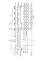
図13は、図11に示したSCANテスト動作を説明するためのタイミングチャートを示す図である。
FIG. 12 is a state transition diagram of the counter shown in FIG. When SCANCLK is 0, this is a 2-bit binary counter that operates in binary notation at the rising edge of SCANIN in the form of 00⇒01⇒10⇒11⇒00⇒ ..., and its MSB is configured as SCANENB. That is, when the counter is 00 and 01 in binary notation, SCANENB is 0, and when the counter is 10 and 11 in binary notation, SCANENB is 1.
FIG. 13 is a timing chart for explaining the SCAN test operation shown in FIG.
(1);SCANINからパルスを入れることでカウンタを2進数表記で10とし、SCANENBを1にして全FFをSCAN動作可能にする(図13ではSCANINからパルス2発を入れることでカウンタを2進数表記で00⇒01⇒10とし、SCANENBを1にして全FFをSCAN動作可能にしている)。
(2);SCANENBが1かつSCANINを所望の0または1にする(図13では1にセットしている。この際カウンタは2進数表記で10⇒11となる)。
(3);SCANENBが1のままでSCANCLKを入れてFFAに所望の値を取り込む(図13では1をとりこむ。このときカウンタは2進数表記で11のまま)。
(1): By inputting a pulse from SCANIN, the counter is set to 10 in binary notation, and SCANENB is set to 1 to enable all FFs to perform SCAN operation (in FIG. 13, by inputting two pulses from SCANIN, the counter is binary) In the notation, 00⇒01⇒10, SCANENB is set to 1, and all FFs are enabled for SCAN operation).
(2); SCANENB is set to 1 and SCANIN is set to a desired 0 or 1 (in FIG. 13, it is set to 1. In this case, the counter becomes 10⇒11 in binary notation).
(3); SCANENB captures a desired value to FF A putting SCANCLK remains 1 (. Fetches one in Figure 13 this time counter remains 11 in binary notation).
(4);SCANENBが1のままでSCANCLKを入れてFFA、FFB、に所望の値を取り込む(図13ではFFA、FFBにそれぞれ0、1をセットしている。このときカウンタは2進数表記で11のまま)。
(5);SCANENBが1かつSCANINを所望の0または1にする。(図13では次にSCANINを1にしてFFA、FFB、FFBにそれぞれ1、0、1を取り込ませるが、その際カウンタが1周して00になりSCANENBが0になってしまうため、その前にSCANINにパルスを3発いれ、カウンタを2進数表記で11⇒00⇒01⇒10とし、SCANENBを1にして全FFをSCAN動作可能にしている。その後SCANINを1にしている。この際カウンタは2進数表記で10⇒11となる)。
(6);SCANENBが1のままでSCANCLKを入れて全FFに所望の値をセットする(図13ではFFA、FFB、FFBにそれぞれ1、0、1をセットしている。この際カウンタは2進数表記で11のまま)。
(4);. SCANENB is set 0 and 1 to the desired capture value (in FIG. 13 FF A, FF B FF A putting SCANCLK remains 1, FF B, this time counter It remains 11 in binary notation).
(5); SCANENB is 1 and SCANIN is set to 0 or 1 as desired. (In FIG. 13, next, SCANIN is set to 1, and FF A , FF B , and FF B are loaded with 1, 0, 1 respectively. At this time, the counter goes around once and becomes 00 and SCANENB becomes 0. Before that, three pulses are sent to SCANIN, the counter is expressed in
(6); SCANENB remains 1 and SCANCLK is inserted and desired values are set in all FFs (in FIG. 13, FF A , FF B and FF B are set to 1, 0 and 1, respectively. The counter remains 11 in binary notation).
(7);SCANINからパルスを入れることでカウンタを2進数表記で00とし、SCANENBを0(=通常パス)にする(図13ではSCANINから1発パルスを入れることでカウンタを2進数表記で11⇒00とし、SCANENBを0(=通常パス)にする)。
(8);SCANENBが0のままでSCANCLKから1CLK入力し、通常パスの出力(=組み合わせ回路の出力)を各FFに取り込む(図13ではFFA、FFB、FFBにそれぞれ組み合わせ回路出力のQA1、QB1、QC1が取り込まれる。このときカウンタはSCANINを1にしたため2進数表記で01になっている)。
(7); By inputting a pulse from SCANIN, the counter is set to 00 in binary notation, and SCANENB is set to 0 (= normal path) (in FIG. 13, by inputting one pulse from SCANIN, the counter is expressed in binary notation. ⇒00 and set SCANENB to 0 (= normal path)).
(8); SCANENB remains 0 and 1 CLK is input from SCANCLK, and the output of the normal path (= output of the combinational circuit) is taken into each FF (in FIG. 13, the combinational circuit output is input to FF A , FF B , and FF B , respectively) Q A1 , Q B1 , and Q C1 are taken in. At this time, since the SCANIN is set to 1, the counter is 01 in binary notation).
(9);SCANINからパルスを入れることでカウンタを2進数表記で10とし、SCANENBを1にして全FFをSCAN動作可能にする(図13ではSCANINからパルス1発を入れることでカウンタを2進数表記で01⇒10とし、SCANENBを1にして全FFをSCAN動作可能にしている)。
(10);SCANENBが1でSCANCLKを入力して全FFの値(QA1、QB1、QC1)をSCANOUTから出力しモニタする(この際同時に全FFに次の所望の値をセットする。図13では0、1、0をそれぞれセットしている)。
(11);上記(8)〜(10)を繰り返す。
(9): By inputting a pulse from SCANIN, the counter is set to 10 in binary notation, and SCANENB is set to 1 so that all FFs can be operated in SCAN (in FIG. 13, by inputting one pulse from SCANIN, the counter is binary) In the notation, 01 => 10, SCANENB is set to 1, and all FFs are enabled for SCAN operation).
(10); SCANENB is 1 and SCANCLK is input, and the values (Q A1 , Q B1 , Q C1 ) of all FFs are output from SCANOUT and monitored (at this time, the next desired value is set to all FFs simultaneously. In FIG. 13, 0, 1, and 0 are set, respectively).
(11); Repeat (8) to (10) above.
本実施例2におけるカウンタは、2bitのカウンタとしたが、カウンタは、1bit以上であればbit数は問わない。また、カウンタの種類は問わない。また、本実施例2は、カウンタの動作は、SCANINのEdgeは立ち上がりとしたがEdgeの向きは問わない。また、SCANENBが0又は1となるカウンタ値もSCAN動作と通常パスが切り替えることができるように自由に決めてよい。カウンタのリセット信号は、本実施例2では、SCANテストを行う際に1とするTESTMODE信号の反転信号をリセットとしたが、通常動作時にSCANENBが1にならないようにすれば構成は問わない。 Although the counter in the second embodiment is a 2-bit counter, the number of bits is not limited as long as the counter is 1 bit or more. Moreover, the kind of counter is not ask | required. In the second embodiment, the counter operation is such that the edge of SCANIN rises, but the direction of Edge does not matter. Also, the counter value at which SCANENB becomes 0 or 1 may be freely determined so that the SCAN operation and the normal path can be switched. In the second embodiment, the counter reset signal is reset when the inverted signal of the TESTMODE signal is set to 1 when the SCAN test is performed. However, the configuration is not limited as long as SCANENB does not become 1 during normal operation.
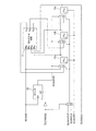
実施例3は、上述した実施例2において1bitカウンタでカウンタを構成した例を示す。
図14は、本発明に係る半導体テスト回路の実施例3を説明するための回路構成図で、SCANINとSCANENBとを共通化したSCANテストを可能にした回路構成図である。なお、図11と同じ機能を有する構成要素には同一に符号を付してある。
SCAN回路がSCANCLKの立ち上がりEdgeで動作するときの新回路の例を図14に示してある。SCANENBを、SCANINをCLKとしたカウンタ23の出力とするように構成する。カウンタ23は、SCANテストを行うTESTMODE=1以外はリセットされる。
The third embodiment shows an example in which the counter is configured by a 1-bit counter in the second embodiment.
FIG. 14 is a circuit configuration diagram for explaining a semiconductor test circuit according to a third embodiment of the present invention, and is a circuit configuration diagram enabling a SCAN test in which SCANIN and SCANENB are shared. In addition, the same code | symbol is attached | subjected to the component which has the same function as FIG.
FIG. 14 shows an example of a new circuit when the SCAN circuit operates at the rising edge of SCANCLK. SCANENB is configured to be the output of the
図15は、図14に示したカウンタの状態遷移図である。SCANCLKが0のとき、SCANINの立ち上がりEdgeで2進数表記で0⇒1⇒…と動作する1bitカウンタであり、その値をSCANENBとして構成する。つまり、カウンタが2進数表記で0の時は、SCANENBが0に、カウンタが2進数表記で1のときは、SCANENBが1となる。
図16は、図14に示したSCANテスト動作を説明するためのタイミングチャートを示す図である。
FIG. 15 is a state transition diagram of the counter shown in FIG. When SCANCLK is 0, this is a 1-bit counter that operates in binary notation at the rising edge of SCANIN, and is configured as SCANENB. That is, when the counter is 0 in binary notation, SCANENB is 0, and when the counter is 1 in binary notation, SCANENB is 1.
FIG. 16 is a timing chart for explaining the SCAN test operation shown in FIG.
(1);SCANINから立ち上がりEdgeを1回いれることでカウンタを2進数表記で1とし、SCANENBを1にして全FFをSCAN動作可能にする(図16ではSCANINから立ち上がりEdgeを1回いれることでカウンタを2進数表記で0⇒1とし、SCANENBを1にして全FFをSCAN動作可能にしている)。
(2);SCANENBが1かつSCANINを所望の0または1にする(図16では1にセットしている。この際カウンタは2進数表記で1のまま)。
(3);SCANENBが1のままでSCANCLKを入れてFFAに所望の値を取り込む(図16では1をとりこむ。このときカウンタは2進数表記で1のまま)。
(1): The rising edge from SCANIN is set to 1 so that the counter is set to 1 in binary notation, SCANENB is set to 1, and all FFs can be operated by SCAN (in FIG. 16, the rising edge is input from SCANIN once. The counter is changed from 0 to 1 in binary notation, and SCANENB is set to 1 so that all FFs can be operated in SCAN).
(2); SCANENB is set to 1 and SCANIN is set to a desired 0 or 1 (in FIG. 16, it is set to 1. In this case, the counter remains 1 in binary notation).
(3); SCANENB captures a desired value to FF A putting SCANCLK remains 1 (. Fetches one in Figure 16 this time counter remains 1 in binary notation).
(4);SCANENBが1のままでSCANCLKを入れてFFA、FFB、に所望の値を取り込む(図13ではFFA、FFBにそれぞれ0、1をセットしている。このときカウンタは2進数表記で1のまま)。
(5);SCANENBが1かつSCANINを所望の0または1にする。(図16では次にSCANINを1にしてFFA、FFB、FFBにそれぞれ1、0、1を取り込ませるが、その際カウンタが1周して0になりSCANENBが0になってしまうため、その前にSCANINにパルスを1発いれ、カウンタを2進数表記で1⇒0とする。その後SCANINを1にしている。この際カウンタは2進数表記で0⇒1となり、SCANENBを1にして全FFをSCAN動作可能にする)。
(6);SCANENBが1のままでSCANCLKを入れて全FFに所望の値をセットする(図13ではFFA、FFB、FFBにそれぞれ1、0、1をセットしている。この際カウンタは2進数表記で1のまま)。
(4);. SCANENB is set 0 and 1 to the desired capture value (in FIG. 13 FF A, FF B FF A putting SCANCLK remains 1, FF B, this time counter It remains 1 in binary notation).
(5); SCANENB is 1 and SCANIN is set to 0 or 1 as desired. (In FIG. 16, next, SCANIN is set to 1, and FF A , FF B , and FF B are loaded with 1, 0, 1 respectively, but at that time, the counter goes round to 0 and SCANENB becomes 0. Before that, one pulse is sent to SCANIN, and the counter is changed from 1 to 0 in binary notation, and then SCANIN is set to 1. At this time, the counter is changed from 0 to 1 in binary notation, and SCANENB is set to 1. All FFs are enabled for SCAN operation).
(6); SCANENB remains 1 and SCANCLK is inserted and desired values are set in all FFs (in FIG. 13, FF A , FF B and FF B are set to 1, 0 and 1, respectively. The counter remains 1 in binary notation).
(7);SCANINから立ち上がりEdgeを1回いれることでカウンタを2進数表記で0とし、SCANENBを0(=通常パス)にする(図16ではSCANINから立ち上がりEdgeを1回いれることでカウンタを2進数表記で1⇒0とし、SCANENBを0(=通常パス)にする)。
(8);SCANENBが0のままでSCANCLKから1CLK入力し、通常パスの出力(=組み合わせ回路の出力)を各FFに取り込む(図16ではFFA、FFB、FFBにそれぞれ組み合わせ回路出力のQA1、QB1、QC1が取り込まれる。このときカウンタはSCANINを1にしたため2進数表記で0のまま)。
(7): The rising edge from SCANIN is set to 0 by setting the counter to 0 in binary notation, and SCANENB is set to 0 (= normal path) (in FIG. 16, the rising edge from SCANIN is set to 1 by setting the rising edge to 1).
(8): SCANENB remains 0 and 1 CLK is input from SCANCLK, and the output of the normal path (= the output of the combinational circuit) is taken into each FF (in FIG. 16, each of the combinational circuit outputs to FF A , FF B , and FF B ) Q A1 , Q B1 , and Q C1 are taken in. At this time, the counter is set to 1 in SCANIN and remains 0 in binary notation).
(9);SCANINから立ち上がりEdgeを1回いれることでカウンタを2進数表記で1とし、SCANENBを1にして全FFをSCAN動作可能にする(図16ではSCANINから立ち上がりEdgeを1回いれることでカウンタを2進数表記で0⇒1とし、SCANENBを1にして全FFをSCAN動作可能にしている)。
(10);SCANENBが1でSCANCLKを入力して全FFの値(QA1、QB1、QC1)をSCANOUTから出力しモニタする(この際同時に全FFに次の所望の値をセットする。図16では0、1、0をそれぞれセットしている)。
(11);上記(8)〜(10)を繰り返す。
(9); The rising edge from SCANIN is set to 1 so that the counter is 1 in binary notation, SCANENB is set to 1, and all FFs can be operated by SCAN (in FIG. 16, the rising edge is input from SCANIN once. The counter is changed from 0 to 1 in binary notation, and SCANENB is set to 1 so that all FFs can be operated in SCAN).
(10); SCANENB is 1 and SCANCLK is input, and the values (Q A1 , Q B1 , Q C1 ) of all FFs are output from SCANOUT and monitored (at this time, the next desired value is set to all FFs simultaneously. In FIG. 16, 0, 1, and 0 are set, respectively.
(11); Repeat (8) to (10) above.
このような上記構成例1〜3により、SCANINとSCANENBを共通化することでピン数の削減ができる。また、従来技術とは異なり、SCANENB用FFは、SCANCLKで動作しないため、SCAN回路は、一般のSCAN回路と同様にSCANCLKの立ち上がりと立下りEdgeで動作するFFが混在してもよく、設計に自由度が増す。例えば、SCAN回路を全てSCANCLKの立ち上がりEdgeのみで動作させる場合、従来技術とは異なり、SCANCLKの立下りEdgeをSCANENB用のFFに使用しないため、このFF用のセットアップタイムが不要となり、SCANCLKのHiの幅を短くできるため、テスト時間の削減ができる。
同様に、SCAN回路を全てSCANCLKの立ち下がりEdgeのみで動作させる場合、従来技術とは異なり、SCANCLKの立ち上がりEdgeをSCANENB用に使用しないため、FFのセットアップタイムが不要となり、SCANCLKのLowの幅を短くできるため、テスト時間の削減ができる。
With the above configuration examples 1 to 3, the number of pins can be reduced by sharing SCANIN and SCANENB. Unlike the conventional technology, the SCANENB FFs do not operate with SCANCLK. Therefore, the SCAN circuit may be mixed with FFs that operate with the rising and falling edges of SCANCLK in the same way as general SCAN circuits. Increased freedom. For example, when all the SCAN circuits are operated only by the rising edge of SCANCLK, unlike the prior art, the falling edge of SCANCLK is not used for the FF for SCANENB, so the setup time for this FF becomes unnecessary, and the SCANCLK Hi The test time can be reduced because the width of the test can be shortened.
Similarly, when all the SCAN circuits are operated only by the falling edge of SCANCLK, unlike the prior art, the rising edge of SCANCLK is not used for SCANENB, so the setup time of FF becomes unnecessary, and the width of SCANCLK Low is increased. Since it can be shortened, the test time can be reduced.
次に、本発明の半導体テスト回路を組み入れたICチップについて説明する。
本発明のICチップは、複数のフリップフロップと組み合わせ回路とを有するデジタルブロックを、スキャンクロックと、スキャンデータ信号と、スキャンイネーブル信号と、によりスキャンテストを行うICチップである。
スキャンクロックが入力される第1のPAD(SCANCLK)と、スキャンデータ信号が入力される第2のPAD(SCANIN)と、第2のPADに接続され、スキャンデータ信号からスキャンイネーブル信号を出力するカウンタと、を備えている。
また、カウンタのクロックラインに、第2のPADが接続され、カウンタの第1のリセットラインに、第1のPADが論理素子を介して接続されている。
また、スキャンデータ信号は、複数のフリップフロップがスキャンクロックに同期して取り込むデータ信号と、複数のフリップフロップに入力されるスキャンクロックが配されない区間に配されるパルス信号と、を有している。
Next, an IC chip incorporating the semiconductor test circuit of the present invention will be described.
The IC chip of the present invention is an IC chip that performs a scan test on a digital block having a plurality of flip-flops and a combinational circuit using a scan clock, a scan data signal, and a scan enable signal.
A first PAD (SCANCLK) to which a scan clock is input, a second PAD (SCANIN) to which a scan data signal is input, and a counter that is connected to the second PAD and outputs a scan enable signal from the scan data signal And.
The second PAD is connected to the counter clock line, and the first PAD is connected to the first reset line of the counter via a logic element.
Further, the scan data signal includes a data signal captured by the plurality of flip-flops in synchronization with the scan clock, and a pulse signal disposed in a section where the scan clock input to the plurality of flip-flops is not disposed. .
また、データ信号を複数のフリップフロップに、スキャンクロックに同期して設定するために順次データが入力された後、次にスキャンクロックが配されるまでの間に、パルス信号が配される。
また、次のスキャンクロックが配された後、別のデータ信号を複数のフリップフロップに、スキャンクロックに同期して設定するために順次データが入力されるまでの間に、パルス信号が配される。
このような構成により、設計の自由度が高く、また、テスト時間が短い半導体テスト回路を組み入れたICチップを実現することができる。
In addition, a pulse signal is arranged after the data is sequentially input to set the data signal to the plurality of flip-flops in synchronization with the scan clock until the next scan clock is arranged.
In addition, after the next scan clock is arranged, a pulse signal is arranged until data is sequentially input in order to set another data signal to a plurality of flip-flops in synchronization with the scan clock. .
With such a configuration, an IC chip incorporating a semiconductor test circuit with a high degree of design freedom and a short test time can be realized.
1 組み合わせ回路
2a,2b,2c,12a,12b,12c 第1乃至第3のフリップフロップ(FFA、FFB、FFC)
3 フリップフロップ(FFENB)
11 組み合わせ回路
13,23 カウンタ
1
3 Flip-flop (FF ENB )
11
Claims (12)
スキャンイネーブル信号に基づいて、通常動作とスキャンデータ信号が入力されるシフトレジスタを構成するスキャン動作とを選択する選択回路を有する複数のフリップフロップ(12a〜12c)と、
前記スキャンデータ信号が入力されて前記複数のフリップフロップへ出力する組み合わせ回路(11)と、
前記スキャンデータ信号が入力されて前記スキャンイネーブル信号を出力するカウンタ(13)と、
を備える半導体テスト回路。 In a semiconductor test circuit having a test mode for detecting a failure of a digital circuit,
A plurality of flip-flops (12a to 12c) having selection circuits for selecting a normal operation and a scan operation constituting a shift register to which a scan data signal is input based on the scan enable signal;
A combinational circuit (11) that receives the scan data signal and outputs it to the plurality of flip-flops;
A counter (13) that receives the scan data signal and outputs the scan enable signal;
A semiconductor test circuit comprising:
前記カウンタにおいて、前記カウンタ制御信号により、前記スキャンイネーブル信号が制御される請求項1に記載の半導体テスト回路。 The scan data signal includes a data signal that the plurality of flip-flops captures in synchronization with a scan clock, and a counter control signal that is disposed in a section in which the scan clock input to the plurality of flip-flops is not disposed. ,
The semiconductor test circuit according to claim 1, wherein the scan enable signal is controlled by the counter control signal in the counter.
前記カウンタにおいて、前記カウンタ制御信号により、前記スキャンイネーブル信号が立ち上がる又は立ち下がる請求項1又は2に記載の半導体テスト回路。 The scan data signal includes a data signal that the plurality of flip-flops captures in synchronization with a scan clock, and a counter control signal that is disposed in a section in which the scan clock input to the plurality of flip-flops is not disposed. ,
3. The semiconductor test circuit according to claim 1, wherein, in the counter, the scan enable signal rises or falls according to the counter control signal.
前記データ信号と前記スキャンクロック信号により、第1の状態と第2の状態の遷移を繰り返し、また、第3の状態と第4の状態の遷移を繰り返し、
前記カウンタ制御信号により、前記第1の状態又は前記第2の状態から、前記第3の状態又は第4の状態への遷移、または、前記第3の状態又は前記第4の状態から、前記第1の状態又は第2の状態への遷移を行い、
前記第1の状態又は前記第2の状態に対応するカウント値が通常動作に対応する前記イネーブル信号であり、前記第3の状態又は前記第4の状態に対応するカウント値がスキャン動作に対応する前記イネーブル信号である請求項4に記載の半導体テスト回路。 The counter transits at least four states;
According to the data signal and the scan clock signal, the transition between the first state and the second state is repeated, and the transition between the third state and the fourth state is repeated.
The counter control signal causes the transition from the first state or the second state to the third state or the fourth state, or from the third state or the fourth state. Make a transition to state 1 or state 2,
The count value corresponding to the first state or the second state is the enable signal corresponding to the normal operation, and the count value corresponding to the third state or the fourth state corresponds to the scan operation. The semiconductor test circuit according to claim 4, wherein the enable signal is the enable signal.
前記スキャンイネーブル信号は、前記カウンタのカウント値のMSB又はLSBである請求項1〜6のいずれか一項に記載の半導体テスト回路。 The counter is a 2-bit binary counter;
The semiconductor test circuit according to claim 1, wherein the scan enable signal is MSB or LSB of a count value of the counter.
スキャンクロックが入力される第1のPAD(SCANCLK)と、
スキャンデータ信号が入力される第2のPAD(SCANIN)と、
前記第2のPADに接続され、前記スキャンデータ信号から前記スキャンイネーブル信号を出力するカウンタと、
を備えるICチップ。 An IC chip that performs a scan test on a digital block having a plurality of flip-flops and a combinational circuit using a scan clock, a scan data signal, and a scan enable signal,
A first PAD (SCANCLK) to which a scan clock is input;
A second PAD (SCANIN) to which a scan data signal is input;
A counter connected to the second PAD and outputting the scan enable signal from the scan data signal;
IC chip comprising:
前記カウンタの第1のリセットラインに、前記第1のPADが論理素子を介して接続される請求項8に記載のICチップ。 The second PAD is connected to the clock line of the counter;
The IC chip according to claim 8, wherein the first PAD is connected to a first reset line of the counter via a logic element.
Priority Applications (1)
| Application Number | Priority Date | Filing Date | Title |
|---|---|---|---|
| JP2014063880A JP6211971B2 (en) | 2014-03-26 | 2014-03-26 | Semiconductor test circuit and IC chip |
Applications Claiming Priority (1)
| Application Number | Priority Date | Filing Date | Title |
|---|---|---|---|
| JP2014063880A JP6211971B2 (en) | 2014-03-26 | 2014-03-26 | Semiconductor test circuit and IC chip |
Publications (2)
| Publication Number | Publication Date |
|---|---|
| JP2015184265A JP2015184265A (en) | 2015-10-22 |
| JP6211971B2 true JP6211971B2 (en) | 2017-10-11 |
Family
ID=54350934
Family Applications (1)
| Application Number | Title | Priority Date | Filing Date |
|---|---|---|---|
| JP2014063880A Active JP6211971B2 (en) | 2014-03-26 | 2014-03-26 | Semiconductor test circuit and IC chip |
Country Status (1)
| Country | Link |
|---|---|
| JP (1) | JP6211971B2 (en) |
Families Citing this family (1)
| Publication number | Priority date | Publication date | Assignee | Title |
|---|---|---|---|---|
| CN111682867B (en) * | 2020-06-19 | 2024-04-02 | 深圳市麦积电子科技有限公司 | Trigger circuit |
Family Cites Families (7)
| Publication number | Priority date | Publication date | Assignee | Title |
|---|---|---|---|---|
| JP2624169B2 (en) * | 1994-04-15 | 1997-06-25 | 日本電気株式会社 | Logic integrated circuit with scan path |
| JPH0989993A (en) * | 1995-09-27 | 1997-04-04 | Kawasaki Steel Corp | Scan circuit |
| JP2003121499A (en) * | 2001-10-09 | 2003-04-23 | Hitachi Ltd | Semiconductor integrated circuit with built-in test function, storage medium for storing electronic design data comprising test code generation program, test method for semiconductor integrated circuit, test code generation automatic method, and program therefor |
| JP2004347537A (en) * | 2003-05-23 | 2004-12-09 | Matsushita Electric Ind Co Ltd | Semiconductor integrated circuit |
| JP4963196B2 (en) * | 2006-07-12 | 2012-06-27 | ルネサスエレクトロニクス株式会社 | Semiconductor integrated circuit device |
| JP2013036960A (en) * | 2011-08-11 | 2013-02-21 | Renesas Electronics Corp | Delay scan test method, semiconductor device, and semiconductor device design method |
| US8972807B2 (en) * | 2012-05-14 | 2015-03-03 | Texas Instruments Incorporated | Integrated circuits capable of generating test mode control signals for scan tests |
-
2014
- 2014-03-26 JP JP2014063880A patent/JP6211971B2/en active Active
Also Published As
| Publication number | Publication date |
|---|---|
| JP2015184265A (en) | 2015-10-22 |
Similar Documents
| Publication | Publication Date | Title |
|---|---|---|
| CN100442074C (en) | Connect multiple test access port controllers through a single test access port | |
| JP2008275479A (en) | Scan test circuit, scan test control method | |
| JP2010276479A (en) | Semiconductor integrated circuit and test method thereof | |
| CN111624478B (en) | A clock signal control circuit and device | |
| US20160349318A1 (en) | Dynamic Clock Chain Bypass | |
| US9021323B1 (en) | Test techniques and circuitry | |
| US20090240996A1 (en) | Semiconductor integrated circuit device | |
| JPWO2006132329A1 (en) | Microcomputer and its test method | |
| CN101371151B (en) | Reduced pin count scan chain implementation | |
| JP2017015597A (en) | Self-test circuit and data processing circuit in integrated circuit | |
| JP6211971B2 (en) | Semiconductor test circuit and IC chip | |
| JP2009122009A (en) | Test circuit | |
| US20170146600A1 (en) | Scan Logic For Circuit Designs With Latches And Flip-Flops | |
| US7456657B2 (en) | Common input/output terminal control circuit | |
| JP2006145307A (en) | Scan test circuit | |
| CN113391178A (en) | Method and apparatus for detecting defective logic devices | |
| US20100033189A1 (en) | Semiconductor integrated circuit and test method using the same | |
| JP2003121497A (en) | Scan path circuit for logic circuit test and integrated circuit device having the same | |
| US11017135B2 (en) | Scan logic for circuit designs with latches and flip-flops | |
| JP5761819B2 (en) | Scan asynchronous memory element, semiconductor integrated circuit including the same, design method thereof, and test pattern generation method | |
| JP6534592B2 (en) | Scan test circuit and scan test apparatus | |
| JP6459806B2 (en) | Semiconductor integrated circuit | |
| US8887016B1 (en) | IC and a method of testing a transceiver of the IC | |
| CN1793999B (en) | semiconductor integrated circuit | |
| JP2010025703A (en) | Semiconductor device and its test method |
Legal Events
| Date | Code | Title | Description |
|---|---|---|---|
| A621 | Written request for application examination |
Free format text: JAPANESE INTERMEDIATE CODE: A621 Effective date: 20161208 |
|
| TRDD | Decision of grant or rejection written | ||
| A977 | Report on retrieval |
Free format text: JAPANESE INTERMEDIATE CODE: A971007 Effective date: 20170831 |
|
| A01 | Written decision to grant a patent or to grant a registration (utility model) |
Free format text: JAPANESE INTERMEDIATE CODE: A01 Effective date: 20170905 |
|
| A61 | First payment of annual fees (during grant procedure) |
Free format text: JAPANESE INTERMEDIATE CODE: A61 Effective date: 20170914 |
|
| R150 | Certificate of patent or registration of utility model |
Ref document number: 6211971 Country of ref document: JP Free format text: JAPANESE INTERMEDIATE CODE: R150 |
|
| S531 | Written request for registration of change of domicile |
Free format text: JAPANESE INTERMEDIATE CODE: R313531 |
|
| R350 | Written notification of registration of transfer |
Free format text: JAPANESE INTERMEDIATE CODE: R350 |