JP2005283207A - Semiconductor integrated circuit device - Google Patents
Semiconductor integrated circuit device Download PDFInfo
- Publication number
- JP2005283207A JP2005283207A JP2004094490A JP2004094490A JP2005283207A JP 2005283207 A JP2005283207 A JP 2005283207A JP 2004094490 A JP2004094490 A JP 2004094490A JP 2004094490 A JP2004094490 A JP 2004094490A JP 2005283207 A JP2005283207 A JP 2005283207A
- Authority
- JP
- Japan
- Prior art keywords
- terminal
- unused
- output
- test
- input
- Prior art date
- Legal status (The legal status is an assumption and is not a legal conclusion. Google has not performed a legal analysis and makes no representation as to the accuracy of the status listed.)
- Granted
Links
Images


Classifications
-
- G—PHYSICS
- G01—MEASURING; TESTING
- G01R—MEASURING ELECTRIC VARIABLES; MEASURING MAGNETIC VARIABLES
- G01R31/00—Arrangements for testing electric properties; Arrangements for locating electric faults; Arrangements for electrical testing characterised by what is being tested not provided for elsewhere
- G01R31/28—Testing of electronic circuits, e.g. by signal tracer
- G01R31/317—Testing of digital circuits
- G01R31/3181—Functional testing
- G01R31/3185—Reconfiguring for testing, e.g. LSSD, partitioning
- G01R31/318533—Reconfiguring for testing, e.g. LSSD, partitioning using scanning techniques, e.g. LSSD, Boundary Scan, JTAG
- G01R31/318572—Input/Output interfaces
-
- G—PHYSICS
- G01—MEASURING; TESTING
- G01R—MEASURING ELECTRIC VARIABLES; MEASURING MAGNETIC VARIABLES
- G01R31/00—Arrangements for testing electric properties; Arrangements for locating electric faults; Arrangements for electrical testing characterised by what is being tested not provided for elsewhere
- G01R31/28—Testing of electronic circuits, e.g. by signal tracer
- G01R31/317—Testing of digital circuits
- G01R31/31712—Input or output aspects
Landscapes
- Engineering & Computer Science (AREA)
- General Engineering & Computer Science (AREA)
- Physics & Mathematics (AREA)
- General Physics & Mathematics (AREA)
- Semiconductor Integrated Circuits (AREA)
- Tests Of Electronic Circuits (AREA)
Abstract
Description
本発明は、外部端子数が多い場合であっても、内部回路の接続試験を行うことができる半導体集積回路装置に関する。 The present invention relates to a semiconductor integrated circuit device capable of performing a connection test for internal circuits even when the number of external terminals is large.
従来、特に組合せ回路からなる論理LSI(Large Scale integrated Circuit:大規模集積回路)においては、回路機能のテスト容易化のため、LSI内部にテスト専用回路であるスキャンテスト回路を有し、スキャンパス方式によるテストを実施することにより組合せ回路が正常に動作していることを確認するものが広く用いられている。 Conventionally, a logic LSI (Large Scale integrated circuit) composed of a combinational circuit has a scan test circuit, which is a dedicated test circuit, in the LSI for easy test of the circuit function. It is widely used to confirm that the combinational circuit is operating normally by performing the test according to the above.
このスキャンテスト回路は、スキャン・フリップフロップを直列に接続したスキャンパス回路チエーンで構成され、シフトレジスタとして動作する。このスキャンテスト回路はLSIの外部又は内部からスキャンテスト用のデータ(スキャンテストパターン)であるスキャンイン信号を入力するスキャンイン端子(スキャンテスト入力端子)と、LSIの外部からスキャンパステスト用のクロックを入力するスキャンクロック端子と、スキャンテストの結果であるスキャンテスト出力データが出力されるスキャンアウト端子とを有している。 This scan test circuit is composed of a scan path circuit chain in which scan flip-flops are connected in series, and operates as a shift register. This scan test circuit includes a scan-in terminal (scan test input terminal) for inputting a scan-in signal as scan test data (scan test pattern) from outside or inside the LSI, and a clock for scan path test from outside the LSI. And a scan-out terminal from which scan test output data as a result of the scan test is output.
スキャンパス方式は、テストモード(シフトモード)時に、スキャンイン端子を介してテスト用のスキャンテストパターンを入力(以下、スキャンイン)し、クロック端子にテスト用のスキャンクロックを入力し、そのデータをLSI内部の組み合わせ回路により論理演算させ、その演算結果である所定の期待値がスキャンテスト出力データとしてスキャンアウト端子から出力(以下、スキャンアウト)されることを確認することにより、組合せ回路が正常に動作していることを確認するものである。すなわち、スキャンアウトされたデータが予め計算した期待値通りであれば組合せ回路に不良はなく、期待値通りでなければ製造不良があると判定する。このように、スキャンテスト回路を採用することで、回路内部を組合せ回路として分離することができ、テストが容易になる。 In the scan path method, in the test mode (shift mode), a test scan test pattern is input via the scan-in terminal (hereinafter referred to as scan-in), a test scan clock is input to the clock terminal, and the data is input. The logic circuit is operated by the combinational circuit inside the LSI, and the combinational circuit is operated normally by confirming that the predetermined expected value as the calculation result is output as scan test output data from the scan-out terminal (hereinafter referred to as scan-out). This is to confirm that it is operating. That is, it is determined that there is no defect in the combinational circuit if the scanned-out data is in accordance with the expected value calculated in advance, and that there is a manufacturing defect if not in the expected value. In this way, by employing the scan test circuit, the inside of the circuit can be separated as a combinational circuit, and the test becomes easy.
ところで、このようなLSIにおけるテストでは、LISの外部信号数(外部端子)が、LSIのテストを行うためのテスタの信号数(テストピン)よりも多い場合には、テストピンが多いテスタ(以下、多ピンテスタという。)を新規に導入するのが一般的である。しかしながらこの多ピンテスタを導入するには、新規に設備を導入する必要があり、かつ多ピンテスタは極めて高価な装置であるため、多数の外部端子を有するLSIに比して少ないテストピンのテスタにてテストを行う方法が望まれる。 By the way, in such an LSI test, when the number of LIS external signals (external terminals) is larger than the number of tester signals (test pins) for testing the LSI, the tester having many test pins (hereinafter referred to as the test pins). It is common to introduce a new multi-pin tester). However, in order to introduce this multi-pin tester, it is necessary to introduce a new facility, and the multi-pin tester is an extremely expensive device. Therefore, a tester having fewer test pins than an LSI having a large number of external terminals can be used. A method of testing is desired.
そのような方法として、例えば特許文献1には、多ピン化された場合でも安価で容易に接続試験を行うことができる集積回路及びそのテスト方法が開示されている。この特許文献1に記載の技術においては、集積回路装置内にバウンダリスキャン回路が設けられていると共に、双方向端子パッドを含む入力端子パッドには、入力パッドが、双方向端子パッドを含む出力端子パッドには動作制御信号に基づいてON・OFFする出力バッファが設けられ、TAB(Tape Automated Bonding)テープに実装された場合に、入力端子パッド及び出力端子パッドは短絡用配線によって短絡される。ここで、出力バッファは動作制御信号に基づいてON・OFFするため、出力端子については出力の競合が起こらず、バウンダリスキャンセルにスキャン端子を介してデータを設定した後、1つの出力端子パッドに対応する出力バッファをOFFさせスキャンセルに設定されたデータを出力バッファ及び短落用配線を介して入力端子パッドに送り、更に入力パッドを介してこの入力パッドに対応するスキャンセルにて観測することにより接続試験を実行する。これにより、ピン数が多くなった場合でも接続試験を可能とするものである。 As such a method, for example, Patent Document 1 discloses an integrated circuit that can easily perform a connection test at a low cost even when the number of pins is increased, and a test method therefor. In the technique disclosed in Patent Document 1, a boundary scan circuit is provided in an integrated circuit device, and an input terminal pad including a bidirectional terminal pad includes an output terminal including the bidirectional terminal pad. The pad is provided with an output buffer that is turned ON / OFF based on an operation control signal. When the pad is mounted on a TAB (Tape Automated Bonding) tape, the input terminal pad and the output terminal pad are short-circuited by a short-circuit wiring. Here, since the output buffer is turned ON / OFF based on the operation control signal, there is no output contention for the output terminal, and after setting data to the boundary scan cell via the scan terminal, one output terminal pad is set. Turn off the corresponding output buffer and send the data set to scan cell to the input terminal pad via the output buffer and short drop wiring, and further observe the scan cell corresponding to this input pad via the input pad Execute the connection test. This enables a connection test even when the number of pins increases.
また、他の方法としては、テストボード上で何本かの入力端子を束ねて、LSIの見かけ上の信号数を減らす手法がある。図7は、従来の集積回路装置のテスト方法を示す図である。図7に示すように、LSI201は、多数の外部端子を有するものとし、図7には、そのうち4つの外部端子であって入力端子2021〜2024を示す。これら入力端子2021〜2024は、それぞれ入力バッファ2031〜2034に接続されている。そして、これら入力端子2021〜2014に入力される4つの信号線2041〜2044がテストボード205にて1本の信号線206に束ねられ、この信号線206にLSIテスタのテストピンが接続され、テスト信号が供給される。
しかしながら、上述の特許文献1に記載の方法では、LSIのパッド部分を従来のロジック回路内部のノードの1つのとして扱うため、各入力パッドから所望のテスト信号を入力して内部回路の接続試験を行うことができないという問題点がある。また、上述したように、テストボード上にて複数の信号線を1つにまとめて一のテスト信号を入力する方法においては、テスタとしては安価な少ピンのテスタを使用することができるものが、信号線を外部で1つにまとめてしまうため、それらの入力端子には同じ値しか入力することができず、LSIの完全な機能テストができないという問題点がある。 However, in the method described in Patent Document 1, the pad portion of the LSI is handled as one of the nodes inside the conventional logic circuit, so that a desired test signal is input from each input pad and a connection test of the internal circuit is performed. There is a problem that it cannot be done. Further, as described above, in the method of inputting a single test signal by combining a plurality of signal lines on the test board, an inexpensive tester having a small number of pins can be used as the tester. Since the signal lines are combined into one outside, only the same value can be input to these input terminals, and there is a problem that a complete function test of the LSI cannot be performed.
本発明は、このような問題点を解決するためになされたものであり、外部端子数が内部論理回路のテストを行うテスタのピン数より多い場合であってもLSI内部の接続テストを可能にする半導体集積回路装置を提供することを目的とする。 The present invention has been made to solve such problems, and enables a connection test inside an LSI even when the number of external terminals is larger than the number of tester pins for testing an internal logic circuit. An object of the present invention is to provide a semiconductor integrated circuit device.
本発明に係る半導体集積回路装置は、複数の外部端子と、前記複数の外部端子に接続される内部回路と、前記複数の外部端子のうちテストモード時に未使用となる未使用外部端子の処理をする未使用端子処理手段とを有することを特徴とする。 The semiconductor integrated circuit device according to the present invention is configured to process a plurality of external terminals, an internal circuit connected to the plurality of external terminals, and an unused external terminal that is unused in the test mode among the plurality of external terminals. And unused terminal processing means.
本発明においては、テストモード時にテスタに接続されない未使用の外部端子の処理をする未使用端子処理手段を有しているため、外部端子全てをテスタに接続できない場合であってもテストを可能にする。 In the present invention, since there is an unused terminal processing means for processing unused external terminals that are not connected to the tester in the test mode, the test can be performed even when all the external terminals cannot be connected to the tester. To do.
また、前記未使用外部端子と前記内部回路の間に設けられ、該未使用外部端子のそれぞれに接続されるスキャン・フリップフロップからなるシフトレジスタを有することができ、この複数のスキャン・フリップフロップにより構成されたシフトレジスタにより内部回路に所望の信号を入力したり、又は内部回路から所望の信号を受け取ることができる。 In addition, it is possible to have a shift register provided between the unused external terminal and the internal circuit and including a scan flip-flop connected to each of the unused external terminals. A desired signal can be input to the internal circuit or received from the internal circuit by the configured shift register.
更に、前記未使用端子処理手段は、前記未使用外部端子のうち入力端子に接続される出力バッファと、当該出力バッファを出力モードに設定可能な未使用端子制御信号を入力する未使用端子制御信号線とを有し、前記テストモード時に未使用端子制御信号により当該入力端子を出力モードに設定することができ、テスタと接続されない入力端子は出力モードに設定されるのでオープン(開放)になることがなく、外部からのノイズの影響で動作が不安定になったり、入力バッファが破壊されることがない。 Further, the unused terminal processing means inputs an output buffer connected to an input terminal among the unused external terminals, and an unused terminal control signal for inputting an unused terminal control signal capable of setting the output buffer to an output mode. In the test mode, the input terminal can be set to the output mode by an unused terminal control signal, and the input terminal not connected to the tester is set to the output mode, so that it is open (open). The operation is not unstable or the input buffer is not destroyed due to external noise.
この場合、前記未使用端子処理手段は、双方向端子に接続される出力バッファを通常モード時に出力モードに設定可能な制御信号及び当該出力バッファをテストモード時に出力モードに設定可能な未使用端子制御信号を入力とする論理回路を有し、前記テストモード時に未使用端子制御信号により当該双方向端子を出力モードに設定するようにしてもよい。 In this case, the unused terminal processing means includes a control signal that can set the output buffer connected to the bidirectional terminal to the output mode in the normal mode, and an unused terminal control that can set the output buffer to the output mode in the test mode. A logic circuit that receives a signal may be included, and the bidirectional terminal may be set to the output mode by an unused terminal control signal in the test mode.
更に、前記未使用端子制御信号線は、前記未使用端子処理手段の出力バッファに共通に接続されたものであって、前記未使用端子制御信号線に接続され前記未使用端子制御信号を入力する切替信号入力端子を有することができ、複数の出力バッファに対して未使用端子制御信号を同時に入力することができる。 Further, the unused terminal control signal line is commonly connected to the output buffer of the unused terminal processing means, and is connected to the unused terminal control signal line and inputs the unused terminal control signal. A switching signal input terminal can be provided, and unused terminal control signals can be simultaneously input to a plurality of output buffers.
また、前記未使用端子処理手段は、前記未使用外部端子のうち双方向端子に接続される出力バッファを出力モードに設定可能な未使用端子制御信号を入力する未使用端子制御信号線を有し、前記テストモード時に未使用端子制御信号により当該双方向端子を出力モードに設定することができ、テスタと接続されない双方向端子が入力モードになることがなく、したがって、外部からのノイズの影響で動作が不安定になったり、入出力バッファの入力バッファが破壊されることがない。 The unused terminal processing means has an unused terminal control signal line for inputting an unused terminal control signal capable of setting an output buffer connected to a bidirectional terminal among the unused external terminals to an output mode. In the test mode, the bidirectional terminal can be set to the output mode by the unused terminal control signal, and the bidirectional terminal not connected to the tester does not enter the input mode. Operation is not unstable and the input / output buffer input buffer is not destroyed.
また、前記未使用端子処理手段は、前記未使用外部端子のうち入力端子及び/又は双方向端子の電位を固定させる電位固定手段とすることができ、テストモード時にはテスタと接続されない未使用外部端子の電位を固定して安定化することができ、外部からのノイズの影響で動作が不安定になったり、入力バッファ、又は入出力バッファの入力バッファから信号が入力されるなどして破壊されることがない。 The unused terminal processing means may be a potential fixing means for fixing the potential of the input terminal and / or the bidirectional terminal among the unused external terminals, and the unused external terminal not connected to the tester in the test mode. Can be stabilized by fixing the potential of the device, and the operation becomes unstable due to the influence of external noise, or the signal is destroyed by input from the input buffer or the input buffer of the input / output buffer. There is nothing.
更に、前記電位固定手段は、前記未使用外部端子に接続される抵抗と、テストモード時に未使用端子制御信号が入力されて前記抵抗を電源電位又はグランド電位に接続するスイッチとを有することができ、未使用端子制御信号によりプルダウン又はプルアップすることができる。 Further, the potential fixing means may include a resistor connected to the unused external terminal, and a switch that inputs an unused terminal control signal and connects the resistor to a power supply potential or a ground potential in a test mode. It can be pulled down or pulled up by an unused terminal control signal.
本発明によれば、外部端子のうちテストモード時に未使用となる未使用外部端子を例えば出力モードに設定するか、電源又はグランド電位に固定するなどする未使用処理手段を有するため、集積回路装置の外部端子数が内部論理回路のテストを行うためのテスタのピン数より多い場合であって、テスタと外部端子全てとを接続できない場合であってもLSI内部の接続テストを行うことができる。 According to the present invention, since the unused external terminals that are unused in the test mode among the external terminals are set to, for example, the output mode or fixed to the power source or the ground potential, the integrated circuit device is provided. Even if the number of external terminals is larger than the number of tester pins for testing the internal logic circuit and the tester cannot be connected to all the external terminals, a connection test inside the LSI can be performed.
以下、本発明を適用した具体的な実施の形態について、図面を参照しながら詳細に説明する。この実施の形態は、ピン数が多い大規模LSIに比してピン数が少ないテスタを使用したLSI内部の接続テストを行うことができるLSIに適用したものである。 Hereinafter, specific embodiments to which the present invention is applied will be described in detail with reference to the drawings. This embodiment is applied to an LSI capable of performing a connection test inside an LSI using a tester having a small number of pins as compared with a large-scale LSI having a large number of pins.
大規模LSIにおいて、LSIの外部信号数、すなわちLSIの内部論理回路のスキャンパステストを行うために使用される外部端子が、LSIのテストを行うための信号数、すなわちテストピンより多い場合にLSIのテストを実行する場合、LSIの一部の端子(外部信号)はテスタに接続されない状態となる。以下、本明細書においては、テスタに接続されない未使用の外部端子を浮き端子という。 In a large-scale LSI, when the number of external signals of the LSI, that is, the number of external terminals used for performing a scan path test of the internal logic circuit of the LSI is larger than the number of signals for performing the LSI test, that is, the test pins, the LSI When this test is executed, some terminals (external signals) of the LSI are not connected to the tester. Hereinafter, in this specification, an unused external terminal that is not connected to the tester is referred to as a floating terminal.
LSIの一部の端子(外部信号)をテスタに接続せず上記浮き端子とする場合、以下の2つの問題が生じる。すなわち、
1.入力端子及び入力モード時の双方向端子は、端子がオープンになるため、ノイズ等により入力バッファが破壊される
2.テスタに繋がない浮き端子から信号の出し入れができないため、LSI全体の十分なテストを行うことができない
When some of the terminals (external signals) of the LSI are not connected to the tester and are used as the floating terminals, the following two problems arise. That is,
1. 1. Since the input terminal and the bidirectional terminal in the input mode are open, the input buffer is destroyed due to noise or the like. Since it is not possible to input and output signals from floating terminals that are not connected to the tester, sufficient testing of the entire LSI cannot be performed.
したがって、本発明の第1の実施の形態においては、浮き端子の入力バッファの破壊防止を図るべく、入力端子及び入力モード時の双方向端子をテストモード時において強制的に出力モードに設定するための未使用端子処理手段を設けると共に、各未使用外部端子にスキャン・フリップフロップSFFを接続し、このフリップフロップ群によるスキャンチェーンを構成し、これを利用して内部回路にテスト信号を入力するものである。 Therefore, in the first embodiment of the present invention, in order to prevent destruction of the input buffer of the floating terminal, the input terminal and the bidirectional terminal in the input mode are forcibly set to the output mode in the test mode. In addition to the unused terminal processing means, a scan flip-flop SFF is connected to each unused external terminal to form a scan chain by this flip-flop group, and a test signal is input to the internal circuit using this It is.
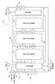
図1は、本実施の形態におけるLSIを示す模式図である。図1に示すように、本実施の形態におけるLSI110は、複数の外部端子のうち、テスト時に未使用となる双方向端子111i、入力端子112j、及び出力端子113kと、双方向端子111i及び入力端子112jに接続続される入出力回路121並びに出力端子113kに接続される出力回路122と、LSI内の論理回路である内部回路130とを有する。内部回路130は、テストモード時には、内部のスキャン・フリップフロップSFF_A〜SFF_Dによりスキャンパス回路が構成され、組み合わせ回路131〜133のスキャンパステストが実行可能に構成される。
FIG. 1 is a schematic diagram showing an LSI in the present embodiment. As shown in FIG. 1, the
また、内部回路130に対してスキャンパステストを行うためのスキャンパステスト信号であるスキャンイン(SCANIN)信号、スキャンパステストのクロック信号であるスキャンクロック(SCANCLK)信号、組み合わせ回路からの出力又はスキャンイン信号かを選択させるスキャンイネーブル(SCANENABLE)信号を入力するそれぞれ外部端子141〜143と、スキャンパステストを行って得られたスキャンアウト(SCANOUT)信号を出力する外部端子144とを有する。
Further, a scan-in (SCANIN) signal that is a scan-path test signal for performing a scan-path test on the
このLSI110においては、例えば入出力回路121と、SFF_A,SFF_Bとの間で組み合わせ回路131のテストを行い、SFF_A,SFF_BとSFF_C,SFF_Dとの間で組み合わせ回路132のテストを行い、SFF_C,SFF_Dと出力回路122との間で組み合わせ回路133のテストを行う。
In this
ここで、本実施の形態におけるLSI110は、全ての外部端子をテスタに接続せずにテストを実行することを可能にするものであり、外部端子と内部回路130との間の入出力回路121、出力回路122に、未使用外部端子のそれぞれに接続されたスキャン・フリップフロップからなるシフトレジスタ(スキャンパス)が構成されている。また、双方向端子111iの入力モード、及び入力端子112jを出力モードに設定するための後述する未使用端子処理部を備えている。
Here, the
すなわち、浮き端子となる外部端子には未使用処理部により出力モードに設定して信号が入力されないようにするため、これらの外部端子と接続される内部回路の入力に所望の信号を入力する手段として上記スキャン・フリップフロップを設ける。 That is, means for inputting a desired signal to the input of the internal circuit connected to these external terminals in order to prevent the external terminals to be floating terminals from being input by setting the output mode by the unused processing unit The above-described scan flip-flop is provided.
また、未使用端子処理部は、未使用端子(浮き端子)のうち、入力端子112jにおいては、出力バッファと、この出力バッファのON・OFFを制御可能なテストモード切替信号としての多ピンテスト切替信号を入力する多ピンテスト切替信号線とからなり、テストモード時には多ピンテスト切替信号により出力バッファをONして出力端子112jを出力モードに設定する。また、浮き端子のうち、双方向端子111iにおいては、双方向端子111iの入出力バッファの出力バッファのON・OFFを制御可能な制御手段を設け、同じく多ピンテスト切替信号により双方向端子111iを出力モードに設定する。したがって、これらの多ピンテスト切替信号線に共通に接続される信号線と、この信号線に接続され多ピンテスト切替信号を入力する多ピンテスト切替信号端子145を有する。
In addition, the unused terminal processing unit, among the unused terminals (floating terminals), has a multi-pin test as a test mode switching signal that can control ON / OFF of the output buffer at the
なお、図1では、簡単のため、テスト信号を入力する端子141〜144及び多ピンテスト切替信号端子145以外は、浮き端子であるとして説明するが、上述した如く、テスタに接続されずに浮き端子となる外部端子は、LSIの外部端子数、回路構成、テスタなどによって異なり、これに限るものではない。また、浮き端子のそれぞれにスキャン・フリップフロップが接続されるものとして説明するが、例えばテスト時にテスタに接続不能な外部端子である浮き端子を上記未使用端子処理部により出力モードに設定できればよく、当該浮き端子がスキャン・フリップフロップに接続されていない場合は、テスト終了後に当該浮き端子にテスタを接続してテストを行うようにしてもよい。すなわち、未使用処理部は、浮き端子となる可能性がある外部端子に設ければよく、その場合は、未使用処理部に共通の多ピンテスト切替信号ではなく、各未使用処理部を個別に動作させる多ピンテスト切替信号を入力するようにすればよい。
In FIG. 1, for the sake of simplicity, it is assumed that the terminals other than the test
次に、本実施の形態における未使用端子処理部について更に詳細に説明する。図2(a)乃至図2(c)は、本実施の形態におけるLSIの外部端子への入出力部分を示す図であって、それぞれ双方向端子、入力端子、出力端子及びその入出力回路又は出力回路部分を拡大して示す回路図である。図2(a)に示すように、本実施の形態におけるLSI110においては、LSIの外部端子のうち、双方向端子111iには、これに接続された入力バッファ2及び出力バッファ3からなる入出力バッファ1と、シフトレジスタを構成するスキャン・フリップフロップSFF4と、入力バッファ2及びSFF4の出力が入力され多ピンテスト切替信号S101によりいずれか一方を選択して内部回路又は次段のSFFへの入力S1021として出力する選択回路5と、出力バッファ3をイネーブルにするコントロール信号(イネーブル信号)S103及び多ピンテスト切替信号S101が入力されその論理和を出力するOR回路6と、コントロール信号S103及びLSI内部の内部論理回路からの出力S104が入力されその排他的論理和が出力されるEXOR回路(exclusive-OR circuit)7とを有する入出力回路が接続されている。SFF4には、EXOR回路7の出力が入力され、SCANCLK信号S1051のタイミングでそのデータを保持し、保持していたデータを出力する。OR回路6は、双方向端子111iを出力モードに設定する未使用端子処理手段を構成する。なお、図2(a)においては、内部回路の出力(EXOR回路7の出力)がSFF4に入力される信号線のみを示すが、SFF4は、前段のSFFからの出力及び内部回路の出力が入力されこれらのいずれかをスキャンイネーブル信号により選択可能なマルチプレクサ及びマルチプレクサにて選択された信号をデータ入力とするフリップフロップとから構成される。
Next, the unused terminal processing unit in the present embodiment will be described in more detail. 2 (a) to 2 (c) are diagrams showing input / output portions to an external terminal of the LSI according to the present embodiment, which are bidirectional terminals, input terminals, output terminals and input / output circuits thereof, respectively. It is a circuit diagram which expands and shows an output circuit portion. As shown in FIG. 2A, in the
また、図2(b)に示すように、本実施の形態におけるLSI110の外部端子のうち入力端子112jには、この入力端子112jに接続された入力バッファ11と、上記SFF4などとシフトレジスタを構成するSFF12と、入力バッファ11の出力及びSFF12の出力が入力され多ピンテスト切替信号S101によりいずれか一方を選択して内部論理回路の入力S1022として出力する選択回路13と、多ピンテスト切替信号102によりON・OFFし、イネーブル状態又はハイインピーダンス状態となる出力バッファ14とを有する入出力回路が接続されている。SFF12は、前段のSFFの出力又は前段のSFFに接続される例えば選択回路5の出力又はスキャンイン信号がデータ入力され、それをSCANCLK信号1052のタイミングで取り込み、保持したデータを選択回路13に出力する。ここで、出力バッファ14及び出力バッファ14に多ピンテスト切替信号S101を入力する信号線とから入力端子112jを出力モードに設定する未使用端子処理手段が構成される。
Further, as shown in FIG. 2 (b), to the
また、図2(c)に示すように、本実施の形態におけるLSIの外部端子のうち出力端子113kは、これ接続される出力バッファ21と、SFF4及びSFF12などとシフトレジスタを構成するSFF22とを有する出力回路が接続される。SFF22は、内部回路からの出力信号S1042及び前段のSFFの出力のいずれか一方をスキャンイネーブル信号にて選択して出力するマルチプレクサを入力に備えるフリップフロップからなり、SCANCLK信号S1053のタイミングでそれを取り込み、保持していたデータを出力する。
Further, as shown in FIG. 2 (c), the
これら双方向端子111iのOR回路6及び選択回路5に入力される多ピンテスト切替信号、並びに入力端子112jの出力バッファ14及び選択回路13に入力される多ピンテスト切替信号は、例えば、共通の信号線に接続し、その信号線に接続した図1に示す多ピンテスト切替信号端子145から供給することができる。この多ピンテスト切替信号S101は、例えば、テストモード時は「Hi」、通常モード時は「Low」となる信号とすることができる。
The multi-pin test switching signal input to the
この多ピンテスト切替信号により、図2(a)に示す出力バッファ3がテストモード時にはONの状態となり、双方向端子111iを強制的に出力モードにすることができる。これにより、テストモード時に双方向端子111iをテスタに接続せず、浮き端子となっていても、双方向端子111iからノイズなどが入力することがなく、したがって入力バッファ2を破壊することを防止する。
By this multi-pin test switching signal, the
また、テストモード時には、内部回路からの出力S1041がSFF4に入力され、スキャンクロックS1051のタイミングにて取り込まれ、選択回路5において多ピンテスト切替信号S101によりSFF4の出力が選択され内部回路の入力S1021となる。一方、通常モード時においては、多ピンテスト切替信号は「Low」となる。この場合、入力モードのときは、コントロール信号が「Low」になり、出力バッファ3はOFFにされ、双方向端子111iからの入力が入力バッファ2を介して選択回路5に入力され、この双方向端子111iからの入力が選択されて内部回路の入力S1021となる。また、通常モードの出力モードのときは、コントロール信号S103がOR回路6を介して出力バッファ3をONにし、内部回路からの出力S1041が出力バッファ3を介して双方向端子111iから出力される。
Further, in the test mode, the output S104 1 from the internal circuit is input to SFF4, taken at scan clock S105 1 timing, the internal circuit output is selected in SFF4 by multi-pin test switch signal S101 in the
また、図2(b)に示すように、入力端子112jにおいては、多ピンテスト切替信号S101により出力バッファ14をONして、入力端子112jを出力モードに設定することができ、このことにより、入力端子112jをオープンにせず、入力バッファ12の破壊を防止することができる。一方、通常モード時には、多ピンテスト切替信号S101は「Low」となり、したがって出力バッファ14もOFFとなり、入力端子112jからの入力が選択回路14にて選択され、内部回路の入力1022となる。
Further, as shown in FIG. 2B, at the
また、図2(c)に示すように、出力端子113kに設けられる出力回路においては、内部回路からの出力1042がテストモード時にはSFF21に取り込まれ、図1に示すスキャンアウト端子144から出力されるか、次段のSFFに入力される。通常モード時には、出力端子113kを介して内部回路からの出力1042が出力される。
Further, as shown in FIG. 2 (c), in the output circuit provided in the
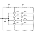
ここで、入出力回路121及び出力回路122に設けられるSFFは、内部回路130のスキャンパス回路に設けられるSFFと同様であり、フリップフロップのデータ入力にマルチプレクサを追加した構成となっている。図3は、一般的なスキャン・フリップフロップSFFの構成を示す図である。図3に示すように、SFF201は、スキャンイン信号かデータ信号かを選択して出力する選択回路(マルチプレクサ)202と、マルチプレクサ202のデータを保持するDフリップフロップ202とを有する。マルチプレクサ202には、スキャンイネーブル信号が入力され、スキャンイン端子又は前段のSFFから出力されるスキャンイン信号、又は組み合わせ回路からの出力データ信号のいずれか一方を選択して出力する。フリップフロップ203はマルチプレクサ202の出力をデータ入力とし、スキャンクロックのタイミングでデータを取り込んだり、出力したりする。その出力Qは、テストモード時にはスキャンアウトとして観測することができる。
Here, the SFF provided in the input /
スキャンパス回路を構成するには、該当する箇所のフリップフロップをこの図3に示すようなスキャン・フリップフロップに置き換え,各スキャン・フリップフロップの間をネットで結んでスキャン・パス(スキャン・チェーン)を構成すればよい。 To configure the scan path circuit, the flip-flops at the corresponding locations are replaced with scan flip-flops as shown in FIG. 3, and the scan flip-flops are connected by a net to form a scan path (scan chain). May be configured.
なお、スキャン手法にはフルスキャンとパーシャルスキャンの2種類があるが、全てのフリップフロップをスキャン・フリップフロップに置き換えるフルスキャンとしてもよく、一部のフリップフロップのみをスキャン・フリップフロップに置き換えパーシャルスキャンとしてもよい。フルスキャンであれば、すべての回路を組み合わせ回路として取り扱えるようになり、テストが非常に容易になる。また、パーシャルスキャンとすれば、チップ面積の増大を抑えることができる。 There are two types of scan methods: full scan and partial scan, but it is also possible to use full scan in which all flip-flops are replaced with scan flip-flops, or partial flip-flops are replaced with scan flip-flops. It is good. With full scan, all circuits can be handled as combinational circuits, which makes testing very easy. Further, if partial scanning is used, an increase in chip area can be suppressed.
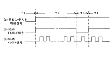
次に、本実施の形態におけるLSI110のスキャンテスト方法について説明する。図4は、テスト方法の手順を示すフローチャートであり、図5(a)〜図5(c)は、それぞれ多ピンテスト切替信号S101の信号レベル、スキャンイネーブル信号、スキャンクロック信号を示すタイミングチャートである。
Next, a scan test method for the
図5(a)に示すように、テスト開始前(期間T1)においては、多ピンテスト切替信号は「Low」となっている。スキャンテストを開始する際には、図4及び図5(a)に示すように、多ピンテスト切替信号をON(「Hi」)にする(ステップS1)。これにより、図2に示す双方向端子111i及び入力端子112jは出力モードに設定される(ステップS2)。以降のスキャンパステストは、通常の方法と同様である。すなわち、図5(b)に示すように、スキャンイネーブル信号をON(「Hi」)にして(ステップS3)、スキャンイン端子から目的のデータ(スキャンイン信号)を入力する。そして、スキャンクロック信号に合わせてシフトレジスタ動作(スキャンシフト)によりSFFを目的の値に設定する(ステップS4、期間T2)。
As shown in FIG. 5A, the multi-pin test switching signal is “Low” before the test is started (period T1). When starting the scan test, as shown in FIGS. 4 and 5A, the multi-pin test switching signal is turned ON (“Hi”) (step S1). Thereby, the
その後、スキャンイネーブル信号をOFF(「Low」)にし、SFFにてデータを取り込み(ステップS5、期間T3)、再びシフトレジスタ動作により(期間T4)、目的のSFFの値をスキャンアウトから観測することができる。なお、テストが終了した場合は、多ピンテスト切替信号を再びOFF(「Low」)にする。 Thereafter, the scan enable signal is turned OFF (“Low”), data is taken in by the SFF (step S5, period T3), and the value of the target SFF is observed from the scan-out again by the shift register operation (period T4). Can do. When the test is completed, the multi-pin test switching signal is turned OFF (“Low”) again.
本実施の形態によれば、外部端子と内部回路130との間にSFFによるスキャンチェーンを設けることで、外部端子を介さずに内部回路130に対してスキャンイン信号を入力することができ、外部端子からスキャンイン信号を入力した場合と同様の試験を行うことができる。したがって、外部端子がテスタのテスタピンより多い場合などにおいては、例えば新しいテスタを準備したり、入力信号をまとめて1つとしたりする必要がなく、所望のテスト信号により内部回路の接続試験を行うことができる。この場合、テストモード時に不使用の浮き端子(未使用外部端子)のうち、入力端子及び双方向端子は、多ピンテスト切替信号により出力モードに設定されるため、テスタに接続されなくてもオープンになることがなく、したがって外部端子に設けられる入力バッファにノイズなどが混入して破壊してしまうことがない。
According to the present embodiment, by providing a scan chain by SFF between the external terminal and the
次に、本発明の第2の実施の形態について説明する。上述の第1の実施の形態においては、入力端子、入力モードの双方向端子を出力モードに設定することで、浮き端子からノイズが入力したりして入力バッファを破壊することを防止したが、本実施の形態においては、浮き端子を電源又はグランド電位に固定しても同様に、入力バッファの破壊を防止することができる。図6は、本実施の形態における外部端子部分を拡大して示す図である。なお、図6に示す本実施の形態において、図2に示す第1の実施の形態と同一の構成要素には同一の符号を付してその詳細な説明は省略する。 Next, a second embodiment of the present invention will be described. In the first embodiment described above, by setting the input terminal and the bidirectional terminal of the input mode to the output mode, it has been prevented that noise is input from the floating terminal and the input buffer is destroyed. In the present embodiment, even when the floating terminal is fixed to the power supply or the ground potential, the destruction of the input buffer can be similarly prevented. FIG. 6 is an enlarged view showing the external terminal portion in the present embodiment. In the present embodiment shown in FIG. 6, the same components as those in the first embodiment shown in FIG. 2 are denoted by the same reference numerals, and detailed description thereof is omitted.
図6(a)に示すように、双方向端子111iは、入出力バッファ1と、SFF4と、双方向端子111iからの入力又はSFF4の出力のいずれか一方を選択して出力する選択回路5とを有する入出力回路と接続される。そして、この双方向端子111iにはプルダウン抵抗8と、一端が接地され他端がプルダウン抵抗8に接続されたスイッチ9とからプルダウンが構成されている。このスイッチ9は、テストモード時に、多ピンテスト切替信号S101によりONになり、双方向端子111iの電位を接地レベルに固定する。
As shown in FIG. 6 (a), the
また、図6(b)に示すように、入力端子112jは、入力バッファ11と、SFF12と、これらいずれかの入力を選択する選択回路13とを有する入出力回路と接続される。そして、この入力端子112jには、プルダウン抵抗15と、一端が接地され、他端が接地されたスイッチ16とからプルダウンが構成されている。このスイッチ15も、テストモード時にスイッチ9と同様に、多ピンテスト切替信号S101によりONになり、入力端子112jの電位を接地レベル固定する。図6(c)に示す出力端子部分の構成は、図2(c)に示す第1の実施の形態の出力端子部分と同様の構成となっている。
Further, as shown in FIG. 6 (b), the
なお、本実施の形態においては、外部端子(双方向端子、入力端子)の電位を固定する手段としてプルダウンを構成するものとしたが、抵抗と、この抵抗と電源電位との間に多ピンテスト切替信号によりON・OFFするスイッチとを設けてプルアップを構成してもよいことは勿論である。 In this embodiment, the pull-down is configured as a means for fixing the potential of the external terminal (bidirectional terminal, input terminal). However, a multi-pin test is performed between the resistor and the resistor and the power supply potential. Of course, a pull-up may be configured by providing a switch that is turned ON / OFF by a switching signal.
本実施の形態においては、テスタの端子数が少ない場合においては、各入力端子と、内部回路との間に、フリップフロップFFを接続し、SCANテストを使用することにより、外部端子からテスト信号を入力した場合と同様の試験を行うことができると共に、図5に示す第1の実施の形態と同様、テストモード時には、多ピンテスト切替信号がONするため、双方向端子111i及び入力端子112jの電位がグランド電位に接続されて安定化されるため、これらの端子がオープンになって外部からのノイズの影響で動作が不安定になったり、入出力バッファの入力バッファが破壊されることを防止することができる。
In this embodiment, when the number of tester terminals is small, a flip-flop FF is connected between each input terminal and the internal circuit, and a test signal is sent from the external terminal by using the SCAN test. A test similar to the case of input can be performed, and, similarly to the first embodiment shown in FIG. 5, in the test mode, the multi-pin test switching signal is turned ON, so the
なお、本発明は上述した実施の形態のみに限定されるものではなく、本発明の要旨を逸脱しない範囲において種々の変更が可能であることは勿論である。 It should be noted that the present invention is not limited to the above-described embodiments, and various modifications can be made without departing from the scope of the present invention.
1 入出力バッファ 2 入力バッファ 3 出力バッファ 4 SFF 5 選択回路 13,14 選択回路 6 OR回路 7 EXOR回路 8,15 プルダウン抵抗 9,16 スイッチ 11,13 入力バッファ 12,14,21 出力バッファ 101 LSI 111i 双方向端子 112j 入力端子 113k 出力端子 121 入出力回路 122 出力回路 130 内部回路
DESCRIPTION OF SYMBOLS 1 Input /
Claims (9)
前記複数の外部端子に接続される内部回路と、
前記複数の外部端子のうちテストモード時に未使用となる未使用外部端子の処理をする未使用端子処理手段と
を有することを特徴とする半導体集積回路装置。 Multiple external terminals,
An internal circuit connected to the plurality of external terminals;
A semiconductor integrated circuit device comprising: unused terminal processing means for processing unused external terminals that are unused in the test mode among the plurality of external terminals.
ことを特徴とする請求項1記載の半導体集積回路装置。 The semiconductor integrated circuit according to claim 1, further comprising a shift register provided between the unused external terminal and the internal circuit and including a scan flip-flop connected to each unused external terminal. apparatus.
ことを特徴とする請求項1又は2に記載の半導体集積回路装置。 The unused terminal processing means includes an output buffer connected to an input terminal among the unused external terminals, and an unused terminal control signal line for inputting an unused terminal control signal capable of setting the output buffer to an output mode. The semiconductor integrated circuit device according to claim 1, wherein the input terminal is set to an output mode by an unused terminal control signal during the test mode.
前記未使用端子制御信号線に接続され前記未使用端子制御信号を入力する切替信号入力端子を有する
ことを特徴とする請求項3記載の半導体集積回路装置。 The unused terminal control signal line is commonly connected to an output buffer of the unused terminal processing means,
The semiconductor integrated circuit device according to claim 3, further comprising a switching signal input terminal that is connected to the unused terminal control signal line and inputs the unused terminal control signal.
ことを特徴とする請求項1記載の半導体集積回路装置。 The unused terminal processing means has an unused terminal control signal line for inputting an unused terminal control signal capable of setting an output buffer connected to a bidirectional terminal among the unused external terminals to an output mode, 2. The semiconductor integrated circuit device according to claim 1, wherein the bidirectional terminal is set to an output mode by an unused terminal control signal in a test mode.
ことを特徴とする請求項1記載の半導体集積回路装置。 The unused terminal processing means can set an output buffer connected to a bidirectional terminal among the unused external terminals to a control signal capable of setting the output mode in the normal mode and the output buffer to the output mode in the test mode. 2. The semiconductor integrated circuit device according to claim 1, further comprising: a logic circuit that receives an unused terminal control signal, wherein the bidirectional terminal is set to an output mode by the unused terminal control signal in the test mode.
を有することを特徴とする請求項1又は2に記載の半導体集積回路装置。 3. The semiconductor integrated circuit according to claim 1, wherein the unused terminal processing unit is a potential fixing unit configured to fix a potential of an input terminal and / or a bidirectional terminal among the unused external terminals. Circuit device.
ことを特徴とする請求項7記載の半導体集積回路装置。 The potential fixing means includes a resistor connected to the unused external terminal, and a switch that receives an unused terminal control signal in a test mode and connects the resistor to a power supply potential or a ground potential. 8. The semiconductor integrated circuit device according to claim 7.
前記未使用端子制御信号線に接続され前記未使用端子制御信号を入力する切替信号入力端子を有する
ことを特徴とする請求項8記載の半導体集積回路装置。 The unused terminal control signal line is commonly connected to a switch of the potential fixing means,
The semiconductor integrated circuit device according to claim 8, further comprising a switching signal input terminal that is connected to the unused terminal control signal line and inputs the unused terminal control signal.
Priority Applications (3)
| Application Number | Priority Date | Filing Date | Title |
|---|---|---|---|
| JP2004094490A JP4610919B2 (en) | 2004-03-29 | 2004-03-29 | Semiconductor integrated circuit device |
| EP05004264A EP1584935A1 (en) | 2004-03-29 | 2005-02-26 | Configuration of unused external pins during the test mode in a semiconductor integrated circuit |
| US11/085,149 US7284171B2 (en) | 2004-03-29 | 2005-03-22 | Integrated circuit device |
Applications Claiming Priority (1)
| Application Number | Priority Date | Filing Date | Title |
|---|---|---|---|
| JP2004094490A JP4610919B2 (en) | 2004-03-29 | 2004-03-29 | Semiconductor integrated circuit device |
Publications (2)
| Publication Number | Publication Date |
|---|---|
| JP2005283207A true JP2005283207A (en) | 2005-10-13 |
| JP4610919B2 JP4610919B2 (en) | 2011-01-12 |
Family
ID=34909424
Family Applications (1)
| Application Number | Title | Priority Date | Filing Date |
|---|---|---|---|
| JP2004094490A Expired - Fee Related JP4610919B2 (en) | 2004-03-29 | 2004-03-29 | Semiconductor integrated circuit device |
Country Status (3)
| Country | Link |
|---|---|
| US (1) | US7284171B2 (en) |
| EP (1) | EP1584935A1 (en) |
| JP (1) | JP4610919B2 (en) |
Cited By (2)
| Publication number | Priority date | Publication date | Assignee | Title |
|---|---|---|---|---|
| JP2009164425A (en) * | 2008-01-08 | 2009-07-23 | Oki Semiconductor Co Ltd | Real-time monitor device and operating method |
| JP2017201256A (en) * | 2016-05-06 | 2017-11-09 | 日置電機株式会社 | Measuring apparatus and measuring method |
Families Citing this family (2)
| Publication number | Priority date | Publication date | Assignee | Title |
|---|---|---|---|---|
| ITVA20050007A1 (en) * | 2005-02-08 | 2006-08-09 | St Microelectronics Srl | DISTRIBUTION CIRCUIT OF A TEST SIGNAL APPLIED ON A PAD OF AN ELECTRONIC DEVICE |
| EP3435100B1 (en) * | 2017-07-24 | 2020-04-01 | TDK-Micronas GmbH | Method for testing an electronic device and an interface circuit therefore |
Citations (4)
| Publication number | Priority date | Publication date | Assignee | Title |
|---|---|---|---|---|
| JPH0587889A (en) * | 1991-09-30 | 1993-04-06 | Fujitsu Ltd | Semiconductor circuit element and test processing method therefor |
| JPH08105944A (en) * | 1994-10-06 | 1996-04-23 | Fujitsu Ltd | Testing method and device for lsi mounted on mcm |
| JP2001066350A (en) * | 1999-08-27 | 2001-03-16 | Fuji Electric Co Ltd | Test method for integrated circuit |
| JP2001320021A (en) * | 2000-05-09 | 2001-11-16 | Yaskawa Electric Corp | Application specific ic testing circuit |
Family Cites Families (9)
| Publication number | Priority date | Publication date | Assignee | Title |
|---|---|---|---|---|
| JPH04213849A (en) * | 1990-12-10 | 1992-08-04 | Fujitsu Ltd | Semiconductor device and method of detecting initial failure thereof |
| US5337254A (en) * | 1991-12-16 | 1994-08-09 | Hewlett-Packard Company | Programmable integrated circuit output pad |
| US5459733A (en) * | 1992-03-20 | 1995-10-17 | National Semiconductor Corporation | Input/output checker for a memory array |
| JP3331712B2 (en) * | 1993-12-21 | 2002-10-07 | セイコーエプソン株式会社 | Semiconductor device |
| US6363505B1 (en) * | 1997-11-14 | 2002-03-26 | Altera Corporation | Programmable control circuit for grounding unused outputs |
| US6016563A (en) * | 1997-12-30 | 2000-01-18 | Fleisher; Evgeny G. | Method and apparatus for testing a logic design of a programmable logic device |
| JP3324583B2 (en) * | 1999-01-08 | 2002-09-17 | セイコーエプソン株式会社 | Semiconductor device and manufacturing method thereof |
| JP3708493B2 (en) * | 2001-05-18 | 2005-10-19 | 株式会社ソニー・コンピュータエンタテインメント | Debug system, semiconductor integrated circuit, semiconductor integrated circuit debugging method, semiconductor integrated circuit debug program, and computer-readable recording medium recording the semiconductor integrated circuit debug program |
| JP2003057309A (en) | 2001-08-16 | 2003-02-26 | Mitsubishi Electric Corp | Semiconductor integrated circuit device |
-
2004
- 2004-03-29 JP JP2004094490A patent/JP4610919B2/en not_active Expired - Fee Related
-
2005
- 2005-02-26 EP EP05004264A patent/EP1584935A1/en not_active Withdrawn
- 2005-03-22 US US11/085,149 patent/US7284171B2/en active Active
Patent Citations (4)
| Publication number | Priority date | Publication date | Assignee | Title |
|---|---|---|---|---|
| JPH0587889A (en) * | 1991-09-30 | 1993-04-06 | Fujitsu Ltd | Semiconductor circuit element and test processing method therefor |
| JPH08105944A (en) * | 1994-10-06 | 1996-04-23 | Fujitsu Ltd | Testing method and device for lsi mounted on mcm |
| JP2001066350A (en) * | 1999-08-27 | 2001-03-16 | Fuji Electric Co Ltd | Test method for integrated circuit |
| JP2001320021A (en) * | 2000-05-09 | 2001-11-16 | Yaskawa Electric Corp | Application specific ic testing circuit |
Cited By (2)
| Publication number | Priority date | Publication date | Assignee | Title |
|---|---|---|---|---|
| JP2009164425A (en) * | 2008-01-08 | 2009-07-23 | Oki Semiconductor Co Ltd | Real-time monitor device and operating method |
| JP2017201256A (en) * | 2016-05-06 | 2017-11-09 | 日置電機株式会社 | Measuring apparatus and measuring method |
Also Published As
| Publication number | Publication date |
|---|---|
| US20050216803A1 (en) | 2005-09-29 |
| EP1584935A1 (en) | 2005-10-12 |
| JP4610919B2 (en) | 2011-01-12 |
| US7284171B2 (en) | 2007-10-16 |
Similar Documents
| Publication | Publication Date | Title |
|---|---|---|
| US6314539B1 (en) | Boundary-scan register cell with bypass circuit | |
| US6861866B2 (en) | System on chip (SOC) and method of testing and/or debugging the system on chip | |
| JP2009515160A (en) | Integrated circuit inspection method and apparatus | |
| JP2007178421A (en) | Shift resistor not using timing-competing boundary scan register by means of two-phase clock control | |
| JPH11231027A (en) | Large-scale integrated circuit and board test method thereof | |
| JP2004110265A (en) | Test facilitating method for semiconductor integrated circuit | |
| US6806731B2 (en) | Semiconductor integrated circuit device and fault-detecting method of a semiconductor integrated circuit device | |
| JP4265934B2 (en) | Scan campus circuit, logic circuit including the same, and integrated circuit test method | |
| JP2006292646A (en) | Method for testing lsi | |
| JP4610919B2 (en) | Semiconductor integrated circuit device | |
| JP2003121497A (en) | Scan path circuit for logic circuit test and integrated circuit device provided with it | |
| JP2005257366A (en) | Semiconductor circuit device and scan test method concerning semiconductor circuit | |
| JP2004004047A (en) | Input/output characterization chain for integrated circuit | |
| JP2007003338A (en) | Semiconductor device, and testing method therefor | |
| JP4416469B2 (en) | Semiconductor integrated circuit and design method thereof | |
| US20050289421A1 (en) | Semiconductor chip | |
| US20040030976A1 (en) | Partial BIST with recording of the connections between individual blocks | |
| KR100532747B1 (en) | Semiconductor intergrated circuit, method for designing the same, and storage medium where design program for semiconductor intergrated circuit is stored | |
| JP2009175154A (en) | Semiconductor integrated circuit and its design method | |
| JP5231065B2 (en) | Scan flip-flop circuit | |
| JPH112664A (en) | Boundary scan register | |
| JPH11281710A (en) | Boundary scan register | |
| JP2874248B2 (en) | Electronic circuit with scan path for diagnostics | |
| JP2000338188A (en) | Testing circuit for semiconductor integrated circuit | |
| JPH07294606A (en) | Self inspecting circuit for semiconductor integrated circuit |
Legal Events
| Date | Code | Title | Description |
|---|---|---|---|
| A621 | Written request for application examination |
Free format text: JAPANESE INTERMEDIATE CODE: A621 Effective date: 20070110 |
|
| A131 | Notification of reasons for refusal |
Free format text: JAPANESE INTERMEDIATE CODE: A131 Effective date: 20100302 |
|
| A521 | Request for written amendment filed |
Free format text: JAPANESE INTERMEDIATE CODE: A523 Effective date: 20100331 |
|
| TRDD | Decision of grant or rejection written | ||
| A01 | Written decision to grant a patent or to grant a registration (utility model) |
Free format text: JAPANESE INTERMEDIATE CODE: A01 Effective date: 20101012 |
|
| A01 | Written decision to grant a patent or to grant a registration (utility model) |
Free format text: JAPANESE INTERMEDIATE CODE: A01 |
|
| A61 | First payment of annual fees (during grant procedure) |
Free format text: JAPANESE INTERMEDIATE CODE: A61 Effective date: 20101013 |
|
| FPAY | Renewal fee payment (event date is renewal date of database) |
Free format text: PAYMENT UNTIL: 20131022 Year of fee payment: 3 |
|
| R150 | Certificate of patent or registration of utility model |
Free format text: JAPANESE INTERMEDIATE CODE: R150 |
|
| LAPS | Cancellation because of no payment of annual fees |