JP6203573B2 - 3D semiconductor device - Google Patents
3D semiconductor device Download PDFInfo
- Publication number
- JP6203573B2 JP6203573B2 JP2013172535A JP2013172535A JP6203573B2 JP 6203573 B2 JP6203573 B2 JP 6203573B2 JP 2013172535 A JP2013172535 A JP 2013172535A JP 2013172535 A JP2013172535 A JP 2013172535A JP 6203573 B2 JP6203573 B2 JP 6203573B2
- Authority
- JP
- Japan
- Prior art keywords
- electrodes
- etching
- semiconductor device
- electrode
- dummy
- Prior art date
- Legal status (The legal status is an assumption and is not a legal conclusion. Google has not performed a legal analysis and makes no representation as to the accuracy of the status listed.)
- Active
Links
Images


Classifications
-
- H—ELECTRICITY
- H10—SEMICONDUCTOR DEVICES; ELECTRIC SOLID-STATE DEVICES NOT OTHERWISE PROVIDED FOR
- H10B—ELECTRONIC MEMORY DEVICES
- H10B41/00—Electrically erasable-and-programmable ROM [EEPROM] devices comprising floating gates
- H10B41/50—Electrically erasable-and-programmable ROM [EEPROM] devices comprising floating gates characterised by the boundary region between the core region and the peripheral circuit region
-
- H—ELECTRICITY
- H01—ELECTRIC ELEMENTS
- H01L—SEMICONDUCTOR DEVICES NOT COVERED BY CLASS H10
- H01L23/00—Details of semiconductor or other solid state devices
- H01L23/48—Arrangements for conducting electric current to or from the solid state body in operation, e.g. leads, terminal arrangements ; Selection of materials therefor
- H01L23/488—Arrangements for conducting electric current to or from the solid state body in operation, e.g. leads, terminal arrangements ; Selection of materials therefor consisting of soldered or bonded constructions
- H01L23/498—Leads, i.e. metallisations or lead-frames on insulating substrates, e.g. chip carriers
-
- H—ELECTRICITY
- H01—ELECTRIC ELEMENTS
- H01L—SEMICONDUCTOR DEVICES NOT COVERED BY CLASS H10
- H01L21/00—Processes or apparatus adapted for the manufacture or treatment of semiconductor or solid state devices or of parts thereof
- H01L21/02—Manufacture or treatment of semiconductor devices or of parts thereof
- H01L21/04—Manufacture or treatment of semiconductor devices or of parts thereof the devices having at least one potential-jump barrier or surface barrier, e.g. PN junction, depletion layer or carrier concentration layer
- H01L21/18—Manufacture or treatment of semiconductor devices or of parts thereof the devices having at least one potential-jump barrier or surface barrier, e.g. PN junction, depletion layer or carrier concentration layer the devices having semiconductor bodies comprising elements of Group IV of the Periodic System or AIIIBV compounds with or without impurities, e.g. doping materials
- H01L21/30—Treatment of semiconductor bodies using processes or apparatus not provided for in groups H01L21/20 - H01L21/26
- H01L21/31—Treatment of semiconductor bodies using processes or apparatus not provided for in groups H01L21/20 - H01L21/26 to form insulating layers thereon, e.g. for masking or by using photolithographic techniques; After treatment of these layers; Selection of materials for these layers
- H01L21/3105—After-treatment
- H01L21/311—Etching the insulating layers by chemical or physical means
- H01L21/31144—Etching the insulating layers by chemical or physical means using masks
-
- H—ELECTRICITY
- H01—ELECTRIC ELEMENTS
- H01L—SEMICONDUCTOR DEVICES NOT COVERED BY CLASS H10
- H01L21/00—Processes or apparatus adapted for the manufacture or treatment of semiconductor or solid state devices or of parts thereof
- H01L21/02—Manufacture or treatment of semiconductor devices or of parts thereof
- H01L21/04—Manufacture or treatment of semiconductor devices or of parts thereof the devices having at least one potential-jump barrier or surface barrier, e.g. PN junction, depletion layer or carrier concentration layer
- H01L21/18—Manufacture or treatment of semiconductor devices or of parts thereof the devices having at least one potential-jump barrier or surface barrier, e.g. PN junction, depletion layer or carrier concentration layer the devices having semiconductor bodies comprising elements of Group IV of the Periodic System or AIIIBV compounds with or without impurities, e.g. doping materials
- H01L21/30—Treatment of semiconductor bodies using processes or apparatus not provided for in groups H01L21/20 - H01L21/26
- H01L21/31—Treatment of semiconductor bodies using processes or apparatus not provided for in groups H01L21/20 - H01L21/26 to form insulating layers thereon, e.g. for masking or by using photolithographic techniques; After treatment of these layers; Selection of materials for these layers
- H01L21/3205—Deposition of non-insulating-, e.g. conductive- or resistive-, layers on insulating layers; After-treatment of these layers
- H01L21/321—After treatment
- H01L21/3213—Physical or chemical etching of the layers, e.g. to produce a patterned layer from a pre-deposited extensive layer
- H01L21/32139—Physical or chemical etching of the layers, e.g. to produce a patterned layer from a pre-deposited extensive layer using masks
-
- H—ELECTRICITY
- H01—ELECTRIC ELEMENTS
- H01L—SEMICONDUCTOR DEVICES NOT COVERED BY CLASS H10
- H01L21/00—Processes or apparatus adapted for the manufacture or treatment of semiconductor or solid state devices or of parts thereof
- H01L21/02—Manufacture or treatment of semiconductor devices or of parts thereof
- H01L21/04—Manufacture or treatment of semiconductor devices or of parts thereof the devices having at least one potential-jump barrier or surface barrier, e.g. PN junction, depletion layer or carrier concentration layer
- H01L21/34—Manufacture or treatment of semiconductor devices or of parts thereof the devices having at least one potential-jump barrier or surface barrier, e.g. PN junction, depletion layer or carrier concentration layer the devices having semiconductor bodies not provided for in groups H01L21/0405, H01L21/0445, H01L21/06, H01L21/16 and H01L21/18 with or without impurities, e.g. doping materials
- H01L21/44—Manufacture of electrodes on semiconductor bodies using processes or apparatus not provided for in groups H01L21/38 - H01L21/428
- H01L21/441—Deposition of conductive or insulating materials for electrodes
-
- H—ELECTRICITY
- H01—ELECTRIC ELEMENTS
- H01L—SEMICONDUCTOR DEVICES NOT COVERED BY CLASS H10
- H01L21/00—Processes or apparatus adapted for the manufacture or treatment of semiconductor or solid state devices or of parts thereof
- H01L21/70—Manufacture or treatment of devices consisting of a plurality of solid state components formed in or on a common substrate or of parts thereof; Manufacture of integrated circuit devices or of parts thereof
- H01L21/71—Manufacture of specific parts of devices defined in group H01L21/70
- H01L21/768—Applying interconnections to be used for carrying current between separate components within a device comprising conductors and dielectrics
- H01L21/76801—Applying interconnections to be used for carrying current between separate components within a device comprising conductors and dielectrics characterised by the formation and the after-treatment of the dielectrics, e.g. smoothing
- H01L21/76802—Applying interconnections to be used for carrying current between separate components within a device comprising conductors and dielectrics characterised by the formation and the after-treatment of the dielectrics, e.g. smoothing by forming openings in dielectrics
- H01L21/76805—Applying interconnections to be used for carrying current between separate components within a device comprising conductors and dielectrics characterised by the formation and the after-treatment of the dielectrics, e.g. smoothing by forming openings in dielectrics the opening being a via or contact hole penetrating the underlying conductor
-
- H—ELECTRICITY
- H01—ELECTRIC ELEMENTS
- H01L—SEMICONDUCTOR DEVICES NOT COVERED BY CLASS H10
- H01L21/00—Processes or apparatus adapted for the manufacture or treatment of semiconductor or solid state devices or of parts thereof
- H01L21/70—Manufacture or treatment of devices consisting of a plurality of solid state components formed in or on a common substrate or of parts thereof; Manufacture of integrated circuit devices or of parts thereof
- H01L21/71—Manufacture of specific parts of devices defined in group H01L21/70
- H01L21/768—Applying interconnections to be used for carrying current between separate components within a device comprising conductors and dielectrics
- H01L21/76838—Applying interconnections to be used for carrying current between separate components within a device comprising conductors and dielectrics characterised by the formation and the after-treatment of the conductors
- H01L21/76877—Filling of holes, grooves or trenches, e.g. vias, with conductive material
-
- H—ELECTRICITY
- H01—ELECTRIC ELEMENTS
- H01L—SEMICONDUCTOR DEVICES NOT COVERED BY CLASS H10
- H01L23/00—Details of semiconductor or other solid state devices
- H01L23/48—Arrangements for conducting electric current to or from the solid state body in operation, e.g. leads, terminal arrangements ; Selection of materials therefor
- H01L23/488—Arrangements for conducting electric current to or from the solid state body in operation, e.g. leads, terminal arrangements ; Selection of materials therefor consisting of soldered or bonded constructions
- H01L23/498—Leads, i.e. metallisations or lead-frames on insulating substrates, e.g. chip carriers
- H01L23/49838—Geometry or layout
- H01L23/49844—Geometry or layout for devices being provided for in H01L29/00
-
- H—ELECTRICITY
- H01—ELECTRIC ELEMENTS
- H01L—SEMICONDUCTOR DEVICES NOT COVERED BY CLASS H10
- H01L23/00—Details of semiconductor or other solid state devices
- H01L23/52—Arrangements for conducting electric current within the device in operation from one component to another, i.e. interconnections, e.g. wires, lead frames
- H01L23/522—Arrangements for conducting electric current within the device in operation from one component to another, i.e. interconnections, e.g. wires, lead frames including external interconnections consisting of a multilayer structure of conductive and insulating layers inseparably formed on the semiconductor body
- H01L23/5226—Via connections in a multilevel interconnection structure
-
- H—ELECTRICITY
- H01—ELECTRIC ELEMENTS
- H01L—SEMICONDUCTOR DEVICES NOT COVERED BY CLASS H10
- H01L27/00—Devices consisting of a plurality of semiconductor or other solid-state components formed in or on a common substrate
- H01L27/02—Devices consisting of a plurality of semiconductor or other solid-state components formed in or on a common substrate including semiconductor components specially adapted for rectifying, oscillating, amplifying or switching and having at least one potential-jump barrier or surface barrier; including integrated passive circuit elements with at least one potential-jump barrier or surface barrier
- H01L27/04—Devices consisting of a plurality of semiconductor or other solid-state components formed in or on a common substrate including semiconductor components specially adapted for rectifying, oscillating, amplifying or switching and having at least one potential-jump barrier or surface barrier; including integrated passive circuit elements with at least one potential-jump barrier or surface barrier the substrate being a semiconductor body
- H01L27/06—Devices consisting of a plurality of semiconductor or other solid-state components formed in or on a common substrate including semiconductor components specially adapted for rectifying, oscillating, amplifying or switching and having at least one potential-jump barrier or surface barrier; including integrated passive circuit elements with at least one potential-jump barrier or surface barrier the substrate being a semiconductor body including a plurality of individual components in a non-repetitive configuration
- H01L27/0688—Integrated circuits having a three-dimensional layout
-
- H—ELECTRICITY
- H10—SEMICONDUCTOR DEVICES; ELECTRIC SOLID-STATE DEVICES NOT OTHERWISE PROVIDED FOR
- H10B—ELECTRONIC MEMORY DEVICES
- H10B41/00—Electrically erasable-and-programmable ROM [EEPROM] devices comprising floating gates
- H10B41/20—Electrically erasable-and-programmable ROM [EEPROM] devices comprising floating gates characterised by three-dimensional arrangements, e.g. with cells on different height levels
-
- H—ELECTRICITY
- H10—SEMICONDUCTOR DEVICES; ELECTRIC SOLID-STATE DEVICES NOT OTHERWISE PROVIDED FOR
- H10B—ELECTRONIC MEMORY DEVICES
- H10B43/00—EEPROM devices comprising charge-trapping gate insulators
- H10B43/20—EEPROM devices comprising charge-trapping gate insulators characterised by three-dimensional arrangements, e.g. with cells on different height levels
- H10B43/23—EEPROM devices comprising charge-trapping gate insulators characterised by three-dimensional arrangements, e.g. with cells on different height levels with source and drain on different levels, e.g. with sloping channels
- H10B43/27—EEPROM devices comprising charge-trapping gate insulators characterised by three-dimensional arrangements, e.g. with cells on different height levels with source and drain on different levels, e.g. with sloping channels the channels comprising vertical portions, e.g. U-shaped channels
-
- H—ELECTRICITY
- H10—SEMICONDUCTOR DEVICES; ELECTRIC SOLID-STATE DEVICES NOT OTHERWISE PROVIDED FOR
- H10B—ELECTRONIC MEMORY DEVICES
- H10B43/00—EEPROM devices comprising charge-trapping gate insulators
- H10B43/30—EEPROM devices comprising charge-trapping gate insulators characterised by the memory core region
- H10B43/35—EEPROM devices comprising charge-trapping gate insulators characterised by the memory core region with cell select transistors, e.g. NAND
-
- H—ELECTRICITY
- H10—SEMICONDUCTOR DEVICES; ELECTRIC SOLID-STATE DEVICES NOT OTHERWISE PROVIDED FOR
- H10B—ELECTRONIC MEMORY DEVICES
- H10B43/00—EEPROM devices comprising charge-trapping gate insulators
- H10B43/50—EEPROM devices comprising charge-trapping gate insulators characterised by the boundary region between the core and peripheral circuit regions
-
- H—ELECTRICITY
- H10—SEMICONDUCTOR DEVICES; ELECTRIC SOLID-STATE DEVICES NOT OTHERWISE PROVIDED FOR
- H10B—ELECTRONIC MEMORY DEVICES
- H10B63/00—Resistance change memory devices, e.g. resistive RAM [ReRAM] devices
- H10B63/80—Arrangements comprising multiple bistable or multi-stable switching components of the same type on a plane parallel to the substrate, e.g. cross-point arrays
- H10B63/84—Arrangements comprising multiple bistable or multi-stable switching components of the same type on a plane parallel to the substrate, e.g. cross-point arrays arranged in a direction perpendicular to the substrate, e.g. 3D cell arrays
-
- H—ELECTRICITY
- H01—ELECTRIC ELEMENTS
- H01L—SEMICONDUCTOR DEVICES NOT COVERED BY CLASS H10
- H01L2924/00—Indexing scheme for arrangements or methods for connecting or disconnecting semiconductor or solid-state bodies as covered by H01L24/00
-
- H—ELECTRICITY
- H01—ELECTRIC ELEMENTS
- H01L—SEMICONDUCTOR DEVICES NOT COVERED BY CLASS H10
- H01L2924/00—Indexing scheme for arrangements or methods for connecting or disconnecting semiconductor or solid-state bodies as covered by H01L24/00
- H01L2924/0001—Technical content checked by a classifier
- H01L2924/0002—Not covered by any one of groups H01L24/00, H01L24/00 and H01L2224/00
Description
本発明は、半導体装置に関し、より具体的には、積層された電極を利用して製造される3次元半導体装置に関する。 The present invention relates to a semiconductor device, and more specifically, to a three-dimensional semiconductor device manufactured using stacked electrodes.
消費者が要求する優れた性能及び低廉な価額を充足させるために半導体装置の集積度を増加させることが要求されている。
メモリ半導体装置の場合、その集積度は製品の価額を決定する重要な要因であるので、特に増加した集積度が要求されている。
従来の2次元又は平面的なメモリ半導体装置の場合、その集積度は単位メモリセルが占有する面積によって主に決定されるので、微細パターン形成技術の水準に大きく影響を受ける。
In order to satisfy the excellent performance and low price required by consumers, it is required to increase the degree of integration of semiconductor devices.
In the case of a memory semiconductor device, the degree of integration is an important factor that determines the price of a product, and thus an increased degree of integration is required.
In the case of a conventional two-dimensional or planar memory semiconductor device, the degree of integration is mainly determined by the area occupied by the unit memory cell, and thus is greatly influenced by the level of fine pattern formation technology.
しかし、パターンの微細化のためには超高価の装備が必要するので、2次元メモリ半導体装置の集積度は増加しているが、相変わらず制限的である。
このような限界を克服するための代案として、3次元に配列されたメモリセルを具備する半導体装置(以下、3次元メモリ素子)が提案されている。
3次元メモリ素子の場合、メモリセルのみならず、これらに接近するための配線(例えば、ワードライン又はビットライン)もやはり3次元に配列される。
従って、電極等の占有面積をより減らす工夫が求められているという問題がある。
However, since ultra-high cost equipment is required for pattern miniaturization, the degree of integration of the two-dimensional memory semiconductor device is increasing, but it is still limited.
As an alternative for overcoming such a limitation, a semiconductor device (hereinafter, referred to as a three-dimensional memory element) having memory cells arranged in three dimensions has been proposed.
In the case of a three-dimensional memory device, not only the memory cells but also wirings (for example, word lines or bit lines) for accessing them are arranged three-dimensionally.
Therefore, there is a problem that a device for further reducing the occupied area of the electrode or the like is required.
本発明は上記従来の3次元半導体装置における問題点に鑑みてなされたものであって、本発明の目的は、電極の階段形連結構造の占有面積を減らすことができる3次元半導体装置を提供することにある。
また、本発明の他の目的は、階段形連結構造を有する電極が配置された3次元半導体装置、電極連結のための面積を減らすことができる3次元半導体装置を提供することにある。
The present invention has been made in view of the above-described problems in the conventional three-dimensional semiconductor device, and an object of the present invention is to provide a three-dimensional semiconductor device capable of reducing the area occupied by the stepped connection structure of electrodes. There is.
Another object of the present invention is to provide a three-dimensional semiconductor device in which electrodes having a stepped connection structure are arranged, and a three-dimensional semiconductor device capable of reducing the area for electrode connection.
上記目的を達成するためになされた本発明による3次元半導体装置は、基板上に順次に積層された複数の電極を含む電極構造体を具備し、前記電極の各々は、その上部に位置し、前記電極の中のいずれか1つの側壁に対して水平に、そして外方に突出された連結部と、前記電極の内の一つの上部又はその他の電極の下部に位置し、これら電極の中のいずれか1つの側壁と共面をなす側壁を有する整列部とを含み、前記電極の中で垂直に互いに隣接する少なくとも2つの前記整列部は、共面をなす側壁を有し、前記電極構造体は、少なくとも1つの第1グループ及び少なくとも1つの第2グループを含み、前記少なくとも1つの第1グループ及び少なくとも1つの第2グループの各々は、前記基板の上部面と垂直になる方向に沿って連続して積層された前記複数の電極の中の複数の電極を含み、前記少なくとも1つの第1グループを構成する前記電極の前記連結部は、前記電極構造体の一側に配置され、前記少なくとも1つの第1グループの前記整列部は前記電極構造体の反対側の他側に配置され、前記少なくとも1つの第2グループを構成する前記電極の前記連結部は、前記電極構造体の前記他側に配置され、前記少なくとも1つの第2グループの前記整列部は前記電極構造体の前記一側に配置され、前記少なくとも1つの第1グループは前記基板上に積層された複数の電極の内の偶数番目の電極からなり、前記少なくとも1つの第2グループは前記基板上に積層された複数の電極の内の奇数番目の電極からなることを特徴とする。 A three-dimensional semiconductor device according to the present invention made to achieve the above object includes an electrode structure including a plurality of electrodes sequentially stacked on a substrate, and each of the electrodes is positioned above the electrode structure. A connecting portion protruding horizontally and outwardly with respect to any one side wall of the electrode, and positioned at one upper portion of the electrode or at the lower portion of the other electrode; An alignment portion having a side wall that is coplanar with any one side wall, and at least two of the alignment portions that are vertically adjacent to each other in the electrode have a side wall that is coplanar, and the electrode structure Includes at least one first group and at least one second group, each of the at least one first group and at least one second group being continuous along a direction perpendicular to the top surface of the substrate. Then product A plurality of electrodes in the plurality of electrodes formed, and the connecting portion of the electrodes constituting the at least one first group is disposed on one side of the electrode structure, and the at least one first The alignment part of the group is disposed on the other side opposite to the electrode structure, and the connection part of the electrodes constituting the at least one second group is disposed on the other side of the electrode structure, The alignment portion of the at least one second group is disposed on the one side of the electrode structure, and the at least one first group is formed from an even-numbered electrode among a plurality of electrodes stacked on the substrate. The at least one second group includes odd-numbered electrodes among a plurality of electrodes stacked on the substrate .
前記少なくとも1つの第1グループ及び少なくとも1つの第2グループの各々を構成する前記電極の積層数は、2〜16の範囲にあることが好ましい。
前記少なくとも1つの第2グループは前記少なくとも1つの第1グループの上部又は下部に配置されることが好ましい。
上記目的を達成するためになされた本発明による3次元半導体装置は、基板上に順次に積層された複数の電極を含む電極構造体を具備し、前記電極の各々は、その上部に位置し、前記電極の中のいずれか1つの側壁に対して水平に、そして外方に突出された連結部と、
前記電極の内の一つの上部又はその他の電極の下部に位置し、これら電極の中のいずれか1つの側壁と共面をなす側壁を有する整列部とを含み、前記電極の中で垂直に互いに隣接する少なくとも2つの前記整列部は、共面をなす側壁を有し、前記電極構造体は、少なくとも1つの第1グループ及び少なくとも1つの第2グループを含み、前記少なくとも1つの第1グループ及び少なくとも1つの第2グループの各々は、前記基板の上部面と垂直になる方向に沿って連続して積層された前記複数の電極の中の複数の電極を含み、前記少なくとも1つの第1グループを構成する前記電極の前記連結部は、前記電極構造体の一側に配置され、前記少なくとも1つの第1グループの前記整列部は前記電極構造体の反対側の他側に配置され、前記少なくとも1つの第2グループを構成する前記電極の前記連結部は、前記電極構造体の前記他側に配置され、前記少なくとも1つの第2グループの前記整列部は前記電極構造体の前記一側に配置され、前記少なくとも1つの第1グループは前記基板上に積層された複数の電極の内の(4n+1)番目及び(4n+2)番目の電極からなり、前記少なくとも1つの第2グループは前記基板上に積層された複数の電極の内の(4n+3)番目及び(4n+4)番目の電極からなり、ここで、前記nは、(4n+4)が前記電極の総積層数より小さい条件を満足させる0又は自然数の中の少なくとも1つであることを特徴とする。
前記複数の電極の各々の前記連結部及び前記整列部は、当該電極の互いに対向する両端部に配置されることが好ましい。
It is preferable that the number of stacked electrodes constituting each of the at least one first group and the at least one second group is in the range of 2 to 16 .
Before SL at least one second group wherein at least one can be placed above or below the first group preferred.
A three-dimensional semiconductor device according to the present invention made to achieve the above object includes an electrode structure including a plurality of electrodes sequentially stacked on a substrate, and each of the electrodes is positioned above the electrode structure. A connecting portion protruding horizontally and outwardly with respect to any one side wall of the electrode;
An alignment portion located on one of the electrodes or below the other electrode and having a side wall coplanar with any one of the electrodes, and perpendicular to each other in the electrode The at least two adjacent alignment portions have coplanar sidewalls, and the electrode structure includes at least one first group and at least one second group, wherein the at least one first group and at least one Each of the one second group includes a plurality of electrodes among the plurality of electrodes continuously stacked along a direction perpendicular to the upper surface of the substrate, and constitutes the at least one first group The connecting portion of the electrode is disposed on one side of the electrode structure, and the alignment portion of the at least one first group is disposed on the other side opposite to the electrode structure. The connection part of the electrodes constituting one second group is disposed on the other side of the electrode structure, and the alignment part of the at least one second group is on the one side of the electrode structure. The at least one first group includes (4n + 1) th and (4n + 2) th electrodes of the plurality of electrodes stacked on the substrate, and the at least one second group is on the substrate. It is composed of the (4n + 3) th and (4n + 4) th electrodes of the plurality of stacked electrodes, where n is 0 or a natural number satisfying the condition that (4n + 4) is smaller than the total number of stacked electrodes. It is characterized by being at least one of them .
It is preferable that the connection part and the alignment part of each of the plurality of electrodes are disposed at opposite ends of the electrode.
前記電極構造体は、第1領域、第2領域、及びこれらの間に介在するアレイ領域を含み、前記連結部及び前記整列部の各々は、前記第1及び第2領域の中のいずれか1つの上に配置されることが好ましい。
前記電極構造体の前記アレイ領域を垂直に貫通する垂直パターンと、前記垂直パターンと前記複数の電極との間に介在するメモリ要素とをさらに具備することが好ましい。
前記メモリ要素は、電荷格納が可能である物質又は膜構造、あるいは可変抵抗特性を示す物質又は膜構造を含むことが好ましい。
また、上記目的を達成するためになされた本発明による3次元半導体装置は、基板上に順次に積層された複数の電極を含む電極構造体を具備し、前記電極の各々は、その上部に位置し、前記電極の中のいずれか1つの側壁に対して水平に、そして外方に突出された連結部と、前記電極の内の一つの上部又はその他の電極の下部に位置し、これら電極の中のいずれか1つの側壁と共面をなす側壁を有する整列部とを含み、前記電極の中で垂直に互いに隣接する少なくとも2つの前記整列部は、共面をなす側壁を有し、前記複数の電極の内の偶数番目の電極の連結部は、前記電極構造体の一側に配置され、前記複数の電極の内の偶数番目の電極の整列部は前記電極構造体の反対側の他側に配置され、前記複数の電極の内の奇数番目の電極の連結部は、前記電極構造体の前記他側に配置され、前記複数の電極の内の奇数番目の電極の前記整列部は、前記電極構造体の前記一側に配置されることを特徴とする。
また、上記目的を達成するためになされた本発明による3次元半導体装置は、基板上に順次に積層された複数の電極を含む電極構造体を具備し、前記電極の各々は、その上部に位置し、前記電極の中のいずれか1つの側壁に対して水平に、そして外方に突出された連結部と、前記電極の内の一つの上部又はその他の電極の下部に位置し、これら電極の中のいずれか1つの側壁と共面をなす側壁を有する整列部と、前記複数の電極の中のいずれか1つから水平に離隔されて配置され、前記電極と同一の物質で形成される少なくとも1つのダミーパターンとを具備し、前記ダミー部分は、前記複数の電極の側面部と対向する第1ダミー側面部を含み、前記前記複数の電極の側面部及び前記第1ダミー側面部は、互いにミラー対称に配置され、前記前記複数の電極の側面部及び前記第1ダミー側面部の各々は階段形態の断面形状を有し、前記ダミー部分は、前記第1ダミー側面部と対向する第2ダミー側面部をさらに含み、前記基板の上部面の法線に対する前記第2ダミー側面部の角度は、前記法線に対する前記第1ダミー側面部の角度より小さいことを特徴とする。
前記少なくとも1つのダミーパターンは、電気的にフローティング状態にあることが好ましい。
また、上記目的を達成するためになされた本発明による3次元半導体装置は、基板上に順次に積層された複数の電極を含む電極構造体を具備し、前記電極の各々は、その上部に位置し、前記電極の中のいずれか1つの側壁に対して水平に、そして外方に突出された連結部と、前記電極の内の一つの上部又はその他の電極の下部に位置し、これら電極の中のいずれか1つの側壁と共面をなす側壁を有する整列部とを含み、前記電極の中で垂直に互いに隣接する少なくとも2つの前記整列部は、共面をなす側壁を有し、前記電極構造体上に配置されるプラグをさらに具備し、前記電極構造体は、前記複数の電極の中の前記プラグに電気的に接続されたことで構成される本体部分と、前記電極の中の前記プラグから電気的に離隔されて構成されるダミー部分とを含み、前記ダミー部分は、前記本体部分から水平に離隔されて配置され、前記本体部分は、少なくとも1つの本体側面部を含み、前記ダミー部分は、前記本体側面部と対向する第1ダミー側面部を含み、前記本体側面部及び前記第1ダミー側面部は、互いにミラー対称に配置され、前記本体側面部及び前記第1ダミー側面部の各々は階段形態の断面形状を有し、前記ダミー部分は、前記第1ダミー側面部と対向する第2ダミー側面部をさらに含み、前記基板の上部面の法線に対する前記第2ダミー側面部の角度は、前記法線に対する前記第1ダミー側面部の角度より小さいことを特徴とする。
前記第2ダミー側面部は、階段形態の断面形状を有することが好ましい。
前記ダミー部分は、前記基板上に連続して積層された前記複数の電極の中の複数の電極で構成されることが好ましい。
The electrode structure includes a first region, a second region, and an array region interposed therebetween, and each of the connecting portion and the alignment portion is one of the first and second regions. Are preferably arranged on one.
It is preferable to further include a vertical pattern penetrating the array region of the electrode structure vertically, and a memory element interposed between the vertical pattern and the plurality of electrodes.
The memory element preferably includes a material or a film structure capable of storing charges, or a material or a film structure exhibiting variable resistance characteristics.
In addition, a three-dimensional semiconductor device according to the present invention made to achieve the above object includes an electrode structure including a plurality of electrodes sequentially stacked on a substrate, and each of the electrodes is positioned above the electrode structure. A connecting portion protruding horizontally and outwardly with respect to any one of the side walls of the electrode, and one upper portion of the electrode or a lower portion of the other electrode. An alignment part having a side wall coplanar with any one of the side walls, wherein at least two of the alignment parts vertically adjacent to each other in the electrode have a coplanar side wall, The even-numbered electrode connecting portion is disposed on one side of the electrode structure, and the even-numbered electrode alignment portion of the plurality of electrodes is on the other side opposite to the electrode structure. A connecting portion of odd-numbered electrodes among the plurality of electrodes , Disposed on the other side of the electrode structure, the alignment portion of the odd-numbered electrodes of the plurality of electrodes, characterized in that it is arranged on the one side of the electrode structure.
In addition, a three-dimensional semiconductor device according to the present invention made to achieve the above object includes an electrode structure including a plurality of electrodes sequentially stacked on a substrate, and each of the electrodes is positioned above the electrode structure. A connecting portion protruding horizontally and outwardly with respect to any one of the side walls of the electrode, and one upper portion of the electrode or a lower portion of the other electrode. An alignment unit having a side wall that is coplanar with any one of the side walls; and at least one of the plurality of electrodes that is horizontally spaced apart and formed of the same material as the electrode. The dummy portion includes a first dummy side surface portion facing the side surface portions of the plurality of electrodes, and the side surface portions of the plurality of electrodes and the first dummy side surface portion are mutually connected. Arranged in mirror symmetry, said Each of the side surface portions of the plurality of electrodes and the first dummy side surface portion has a step-like cross-sectional shape, and the dummy portion further includes a second dummy side surface portion facing the first dummy side surface portion, The angle of the second dummy side surface portion with respect to the normal line of the upper surface of the substrate is smaller than the angle of the first dummy side surface portion with respect to the normal line .
The at least one dummy pattern is preferably in an electrically floating state.
In addition, a three-dimensional semiconductor device according to the present invention made to achieve the above object includes an electrode structure including a plurality of electrodes sequentially stacked on a substrate, and each of the electrodes is positioned above the electrode structure. A connecting portion protruding horizontally and outwardly with respect to any one of the side walls of the electrode, and one upper portion of the electrode or a lower portion of the other electrode. An alignment portion having a sidewall that is coplanar with any one of the sidewalls, wherein at least two alignment portions that are vertically adjacent to each other in the electrode have coplanar sidewalls, and the electrode A plug disposed on the structure, wherein the electrode structure is electrically connected to the plug in the plurality of electrodes; and the body in the electrode A structure that is electrically isolated from the plug. And a moiety, the dummy portion, said being spaced apart from horizontally from the body portion, said body portion includes at least one side of the body portion, the dummy portion, the opposite to the body side surface portion The main body side surface portion and the first dummy side surface portion are arranged in mirror symmetry with each other, and each of the main body side surface portion and the first dummy side surface portion has a step-like cross-sectional shape, The dummy portion further includes a second dummy side surface portion facing the first dummy side surface portion, and an angle of the second dummy side surface portion with respect to a normal line of the upper surface of the substrate is an angle of the first dummy with respect to the normal line. It is smaller than the angle of the side part .
Second dummy side portion before SL preferably has a cross-sectional shape of the stepped form.
It is preferable that the dummy portion includes a plurality of electrodes among the plurality of electrodes stacked continuously on the substrate.
本発明に係る3次元半導体装置によれば、エッチング深さ及びエッチング領域の両方で差異を有するように実施される、第1パターニング工程及び第2パターニング工程が電極の階段形連結構造を形成するために使用される。
これによって、本発明による3次元半導体装置の階段形連結構造は、共通の単層エッチング方式を通じて具現される従来の構造に比べ、減少した占有面積を有するように形成でき、これを形成する工程もやはり単純化することができるという効果がある。
According to the three-dimensional semiconductor device of the present invention, the first patterning step and the second patterning step, which are performed so as to have a difference in both the etching depth and the etching region, form the stepped connection structure of the electrodes. Used for.
Accordingly, the stepped connection structure of the three-dimensional semiconductor device according to the present invention can be formed to have a reduced occupied area as compared with the conventional structure implemented through a common single-layer etching method, and a process for forming the same is also possible. There is also an effect that it can be simplified.
次に、本発明に係る3次元半導体装置を実施するための形態の具体例を図面を参照しながら説明する。 Next, a specific example of a mode for carrying out the three-dimensional semiconductor device according to the present invention will be described with reference to the drawings.
本発明の長所及び特徴、そしてそれらを達成する方法は添付される図面と共に詳細に後述する実施形態を参照すれば、明確になる。しかし、本発明は以下で開示する実施形態に限定されることではなく、互に異なる多様な形態に具現でき、単なる本実施形態は本発明の開示が完全になるようにし、本発明が属する技術分野で通常の知識を有する者に発明の範疇を完全に知らせるために提供するものであり、本発明は請求項の範疇によって定義されるだけである。明細書の全文に掛けて同一参照符号は同一構成要素を称する。 Advantages and features of the present invention, and methods for achieving them will be apparent with reference to the embodiments described below in detail with reference to the accompanying drawings. However, the present invention is not limited to the embodiments disclosed below, and can be embodied in various forms different from each other. The present embodiments are intended to make the disclosure of the present invention complete, and to which the present invention belongs. It is provided to provide full knowledge of the scope of the invention to those skilled in the art and the invention is only defined by the scope of the claims. Like reference numerals refer to like elements throughout the specification.
本明細書で、導電性膜、半導体膜、又は絶縁性膜等のいずれの物質膜が他の物質膜又は基板“上”に在ると言及する場合に、その物質膜は他の物質膜又は基板上に直接形成され得るか、又はこれらの間にその他の物質膜が介在することもあり得ることを意味する。また、本明細書の多様な実施形態で、第1、第2、第3等の用語が物質膜又は工程段階を記述するために使用するが、これは単なるいずれの特定物質膜又は工程段階を他の物質膜又は他の工程段階と区別させるために使用するだけであり、このような用語によって限定されてはならない。
本明細書で使用する用語は実施形態を説明するためのものであり、本発明を制限しようとすることではない。本明細書で単数形は文句で特別に言及しない限り複数形も含む。明細書で使用する‘含む(comprises)’及び/又は‘含む(comprising)’は言及された構成要素、段階と、動作及び/又は素子は1つ以上の他の構成要素、段階と、動作及び/又は素子の存在又は追加を排除しない。
また、本明細書で記述する実施形態は本発明の理想的な例示図である断面図及び/又は平面図を参考して説明する。図面において、膜及び領域の厚さは技術的内容の効果的な説明のために誇張したものである。したがって、製造技術及び/又は許容誤差等によって例示図の形態が変形され得る。したがって、本発明の実施形態は図示した特定形態に制限されることではなく、製造工程によって生成される形態の変化も含むことである。
In this specification, when any material film such as a conductive film, a semiconductor film, or an insulating film is referred to as being “on” another material film or substrate, the material film may be another material film or It means that it can be formed directly on the substrate, or other material films can be interposed between them. Also, in the various embodiments herein, terms such as first, second, third, etc. are used to describe a material film or process step, which simply refers to any particular material film or process step. It is only used to distinguish it from other material films or other process steps and should not be limited by such terms.
The terminology used herein is for the purpose of describing embodiments and is not intended to limit the invention. In this specification, the singular includes the plural unless specifically stated otherwise. As used herein, “comprises” and / or “comprising” refers to a component, stage, operation and / or element referred to is one or more other components, stages, operations and Do not exclude the presence or addition of elements.
Further, the embodiments described in this specification will be described with reference to cross-sectional views and / or plan views which are ideal exemplary views of the present invention. In the drawings, the thickness of films and regions are exaggerated for effective explanation of technical contents. Accordingly, the form of the illustrative drawing can be modified depending on the manufacturing technique and / or allowable error. Thus, embodiments of the present invention are not limited to the particular forms shown, but are to include variations in form produced by the manufacturing process.
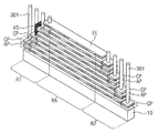
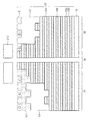
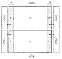
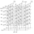
図1は、本発明の一実施形態による半導体装置を例示的に示す斜視図である。
図1を参照すると、電極構造体が連結領域及びアレイ領域RAを含む基板10上に配置される。
例えば、連結領域は、アレイ領域RAの両側に各々位置する第1領域R1及び第2領域R2を包含することができるが、本発明の技術的な思想がこれに限定されることではない。
FIG. 1 is a perspective view illustrating a semiconductor device according to an embodiment of the present invention.
Referring to FIG. 1, the electrode structure is disposed on the
For example, the connection region may include a first region R1 and a second region R2 that are located on both sides of the array region RA, but the technical idea of the present invention is not limited thereto.
電極構造体は、順次に積層された複数の電極ELを含む。
電極ELは、導電性物質(例えば、ドーピングされた半導体又は金属)で形成され得る。一実施形態において、電極ELは同一の物質で形成され得る。
電極ELは、基板10からの距離が遠くなるほど、減少する長さを有するように形成され得る。
これに加えて、平面図上からの観点で見る時、電極ELの中のいずれか1つはその下部に位置する他の電極が占有する領域内に配置される。
The electrode structure includes a plurality of electrodes EL that are sequentially stacked.
The electrode EL can be formed of a conductive material (eg, a doped semiconductor or metal). In one embodiment, the electrode EL may be formed of the same material.
The electrode EL may be formed to have a length that decreases as the distance from the
In addition, when viewed from a plan view, any one of the electrodes EL is disposed in a region occupied by another electrode located below the electrode EL.
例えば、電極ELは、階段形態の積層構造を有するように配置され、電極ELの中のいずれか1つはそれの上部に位置する他の電極によって、隠されない少なくとも1つの端部分(以下、連結部CPと称す)を有することができる。
連結部CPが充分な面積を有するように形成される場合、連結部CPは該当電極と異なる配線との間の電気的な接続のための経路(以下、コンタクト領域)として利用され得る。
For example, the electrode EL is arranged to have a stacked structure in a staircase shape, and any one of the electrodes EL is at least one end portion (hereinafter referred to as a coupling) that is not hidden by the other electrode located on the top of the electrode EL. Part CP).
When the coupling portion CP is formed to have a sufficient area, the coupling portion CP can be used as a path (hereinafter referred to as a contact region) for electrical connection between the corresponding electrode and a different wiring.
本発明の一実施形態によれば、電極ELの中の少なくとも1つはその上部に位置する他の電極と整列された側壁を有する端部分(以下、整列部AP)を有する。
例えば、垂直に隣接する一対の電極ELは、実質的に垂直になる所定の平面VSに整列された(即ち、互いに共面をなす)側壁を有する。
本発明の実施形態で、電極ELの各々は、連結部CP及び整列部APの構造的な特徴を有するように形成された両端を包含する。即ち、電極ELの各々の一端(例えば、連結部CP)はそれの上部に位置する他の電極によって覆われなく、他端(例えば、整列部AP)はそれの上部に位置する他の電極の側壁と共面をなす側壁を有する。
According to an embodiment of the present invention, at least one of the electrodes EL has an end portion (hereinafter referred to as an alignment portion AP) having a side wall aligned with another electrode located on the upper side thereof.
For example, a pair of vertically adjacent electrodes EL have sidewalls aligned with a predetermined plane VS that is substantially vertical (ie, coplanar with each other).
In the embodiment of the present invention, each of the electrodes EL includes both ends formed to have the structural features of the connection part CP and the alignment part AP. That is, one end of each of the electrodes EL (for example, the connecting portion CP) is not covered by the other electrode located on the upper side thereof, and the other end (for example, the alignment portion AP) of the other electrode located on the upper side thereof. A side wall coplanar with the side wall;
本発明の一実施形態によれば、図1に示すように、電極ELの中で偶数番目の電極の各々は第1及び第2領域R1、R2上に各々連結部CP及び整列部APを有するように形成され、電極ELの中で奇数番目の電極の各々は第2及び第1領域R2、R1上に各々連結部CP及び整列部APを有するように形成される。 According to an embodiment of the present invention, as shown in FIG. 1, each of even-numbered electrodes in the electrode EL has a connection part CP and an alignment part AP on the first and second regions R1 and R2, respectively. Each of the odd-numbered electrodes among the electrodes EL is formed to have a connection part CP and an alignment part AP on the second and first regions R2 and R1, respectively.
図2は、本発明の例示的な実施形態による半導体装置の製造方法を概略的に説明するためのフローチャートである。
半導体装置の製造方法は、積層された電極を形成する段階を含み、電極形成段階は、図1に示したように階段形態の連結構造を形成する段階を含む。
以下では図2を参照して本発明の実施形態による階段形態の連結構造を形成する段階を説明する。
図2を参照すれば、基板上に水平膜を順次に積層して積層体を形成する(ステップS1)。
FIG. 2 is a flowchart for schematically explaining a method of manufacturing a semiconductor device according to an exemplary embodiment of the present invention.
The method for manufacturing a semiconductor device includes a step of forming stacked electrodes, and the step of forming an electrode includes a step of forming a step-shaped connection structure as shown in FIG.
Hereinafter, a step of forming a staircase-type connection structure according to an embodiment of the present invention will be described with reference to FIG.
Referring to FIG. 2, a horizontal film is sequentially stacked on a substrate to form a stacked body (step S1).
複数の電極膜及び絶縁膜が交互に積層されて、第1領域及び第2領域を有する積層体を形成する。
積層体は、1つの電極膜の上部面とそれに隣接する他の電極膜の上部面との間の距離に該当する垂直的なピッチを有するように構成される。
一実施形態によれば、図1の電極ELは、水平膜を以下で説明されるパターニング方法を利用してエッチングすることによって得られる結果物であり得る。
即ち、水平膜は、電極ELとして使用され得る。
A plurality of electrode films and insulating films are alternately stacked to form a stacked body having a first region and a second region.
The laminate is configured to have a vertical pitch corresponding to the distance between the upper surface of one electrode film and the upper surface of another electrode film adjacent thereto.
According to one embodiment, the electrode EL of FIG. 1 may be a result obtained by etching a horizontal film using a patterning method described below.
That is, the horizontal film can be used as the electrode EL.
他の実施形態によれば、図1の電極ELは、水平膜を以下で説明されるパターニング方法を利用してエッチングし、水平膜を選択的に除去して空いた空間を形成した後、空いた空間を導電膜で満たすことによって、得られる結果物であり得る。
即ち、水平膜は電極ELが配置される空間を定義する犠牲膜として使用され得る。
According to another embodiment, the electrode EL of FIG. 1 is vacant after the horizontal film is etched using a patterning method described below to form a vacant space by selectively removing the horizontal film. It can be the result obtained by filling the space with a conductive film.
That is, the horizontal film can be used as a sacrificial film that defines a space in which the electrode EL is disposed.
積層体をパターニングして基板の連結領域上に階段形態の連結構造を形成する(ステップS2)。
このステップS2は、選択的なエッチング段階SE及び共通的なエッチング段階CEを包含することができる。
ここで、選択的なエッチング段階SEは、連結領域の特定部分を局所的にエッチングする段階を包含する。反面、共通的なエッチング段階CEは、連結領域の部分の中の複数の部分を同時にエッチングする段階を包含する。一実施形態によれば、選択的なエッチング段階SEでエッチングされる特定部分は、共通的なエッチング段階CEでエッチングされる部分の中の1つに包含され得る。
The stack is patterned to form a staircase-shaped connection structure on the connection region of the substrate (step S2).
This step S2 can include a selective etching stage SE and a common etching stage CE.
Here, the selective etching step SE includes a step of locally etching a specific part of the connection region. On the other hand, the common etching step CE includes simultaneously etching a plurality of portions of the connection region. According to one embodiment, the specific part etched in the selective etching stage SE can be included in one of the parts etched in the common etching stage CE.
階段形態の連結構造を形成する間に、選択的なエッチング段階SE及び共通的なエッチング段階CEは各々少なくとも1回実施され、これらの各々は単層エッチング又は多層エッチングの方法で実施することができる。
単層エッチング方法の場合、選択的又は共通的なエッチング段階(SE或いはCE)はエッチングされる領域が水平膜の各々の垂直的なピッチに該当する第2深さを有するように実施され、多層エッチング方法の場合、選択的又は共通的なエッチング段階(SE或いはCE)は水平膜の中の少なくとも2つの層を連続的にエッチングする方式に実施する。
During the formation of the staircase-shaped connection structure, the selective etching step SE and the common etching step CE are each performed at least once, each of which can be performed in a single-layer etching or multi-layer etching method. .
In the case of a single layer etching method, the selective or common etching step (SE or CE) is performed such that the region to be etched has a second depth corresponding to each vertical pitch of the horizontal film. In the case of an etching method, the selective or common etching step (SE or CE) is carried out in such a manner that at least two layers in the horizontal film are successively etched.
選択的なエッチング段階SE及び共通的なエッチング段階CEは、階段形態の連結構造(例えば、階段式形状形態)を形成するために多様に組み合わせることができ、以下では図3〜図52を参照してそのような組み合わせの例をより詳細に説明する。
これによって、第2領域の第1形状の模様は、第2領域の第2形状の模様と異なることがあり得、その相違は少なくとも垂直的なピッチと同一の大きさであり得る。
The selective etching step SE and the common etching step CE can be variously combined to form a staircase-type connection structure (eg, a staircase-shaped shape), and refer to FIGS. 3 to 52 below. An example of such a combination will be described in more detail.
Thereby, the first shape pattern of the second region may be different from the second shape pattern of the second region, and the difference may be at least as large as the vertical pitch.
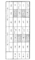
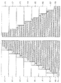
図3は、本発明の例示的な実施形態による半導体装置の製造方法を示すテーブルである。
本発明の実施形態によれば、連結構造を形成するステップS2は、エッチング深さ及びエッチング領域の両方が相違を有するように構成、形成される、第1及び第2パターニング工程を包含することができる。
FIG. 3 is a table showing a method for manufacturing a semiconductor device according to an exemplary embodiment of the present invention.
According to the embodiment of the present invention, the step S2 of forming the connection structure includes first and second patterning processes configured and formed so that both the etching depth and the etching region have a difference. it can.
例えば、第1及び第2パターニング工程の中の少なくとも1つでのエッチング深さは、水平膜の垂直的なピッチの少なくとも2倍である得り、他の1つのエッチング深さは大略水平膜の垂直的なピッチであり得る。
ここで、水平膜の垂直的なピッチは、水平膜の中のいずれか1つとその上部又は下部の他の1つの水平膜の上部面との間の高さの差を意味する。
言い換えれば、第1及び第2パターニング工程の中のいずれか1つは多層エッチングの方法に実施され、その他の1つは単層エッチングの方法に実施される。
例えば、図3に例示的に分類した第1及び第4例は、第1及び第2パターニング工程を各々多層及び単層エッチングの方式に実施し、第2及び第3例は、第1及び第2パターニング工程を各々単層及び多層エッチングの方式に実施する。
For example, the etching depth in at least one of the first and second patterning steps may be at least twice the vertical pitch of the horizontal film, and the other etching depth is approximately that of the horizontal film. It can be a vertical pitch.
Here, the vertical pitch of the horizontal film means a height difference between any one of the horizontal films and the upper surface of the other horizontal film above or below the horizontal film.
In other words, any one of the first and second patterning steps is performed in the multilayer etching method, and the other is performed in the single layer etching method.
For example, in the first and fourth examples categorized in FIG. 3, the first and second patterning processes are performed in a multi-layer and single-layer etching manner, respectively, and in the second and third examples, the first and second patterns are performed. Two patterning steps are performed for each of the single-layer and multi-layer etching methods.
エッチング領域と関連して、本発明の一実施形態によれば、第1及び第2パターニング工程の中の少なくとも1つは、連結領域の各部分に対して実施され、その他の1つは連結領域の特定部分に対して実施される。
例えば、第1及び第2パターニング工程の中のいずれか1つは、第1及び第2領域R1、R2の両方が水平膜をパターニングする共通的なエッチング方式で実施され、その他の1つは、第2領域R2で水平膜をパターニングする選択的なエッチング方式に実施する。
In connection with the etching region, according to one embodiment of the present invention, at least one of the first and second patterning steps is performed for each part of the connection region, and the other one is the connection region. To a specific part of
For example, one of the first and second patterning processes is performed by a common etching method in which both the first and second regions R1 and R2 pattern the horizontal film, and the other one is: The selective etching method for patterning the horizontal film in the second region R2 is performed.
図3を再び参照すると、第1及び第3例の場合、第1パターニング工程は共通的なエッチング方式で実施され、第2パターニング工程は選択的なエッチング方式で実施される。
また、第2及び第4例の場合、第1パターニング工程は選択的なエッチング方式で実施され、第2パターニング工程は共通的なエッチング方式で実施される。
Referring to FIG. 3 again, in the first and third examples, the first patterning process is performed by a common etching method, and the second patterning process is performed by a selective etching method.
In the second and fourth examples, the first patterning process is performed by a selective etching method, and the second patterning process is performed by a common etching method.
一実施形態によれば、共通的なエッチング段階は水平膜を第1及び第2領域R1、R2の両方が数回エッチングされるように実施し、選択的なエッチング段階は水平膜を第2領域で1回エッチングするように実施する。
例えば、第1及び第3例では、第1パターニング工程は共通的なエッチング方式に水平膜を数回エッチングする段階を含み、第2パターニング工程は選択的なエッチング方式に水平膜を1回エッチングする段階を含む。
According to one embodiment, the common etching step performs the horizontal film such that both the first and second regions R1, R2 are etched several times, and the selective etching step performs the horizontal filming on the second region. The etching is performed once.
For example, in the first and third examples, the first patterning process includes a step of etching the horizontal film several times in a common etching method, and the second patterning process etches the horizontal film once in a selective etching method. Including stages.
以下では、図4〜図18を参照して図3で例示的に分類された第1〜第4例による半導体装置の製造方法を説明する。
図4は、本発明の例示的な実施形態の中の1つによる半導体装置の製造方法を説明するためのフローチャートであり、図5〜図8は本発明の例示的な実施形態の中の1つによる半導体装置の製造方法を例示的に説明するための断面図である。
Hereinafter, a method for manufacturing a semiconductor device according to first to fourth examples exemplarily classified in FIG. 3 will be described with reference to FIGS.
FIG. 4 is a flowchart for explaining a method of manufacturing a semiconductor device according to one of the exemplary embodiments of the present invention, and FIGS. 5 to 8 are diagrams illustrating one of the exemplary embodiments of the present invention. It is sectional drawing for demonstrating the manufacturing method of the semiconductor device by two.
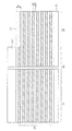
図3〜図5を参照すると、基板10上に水平膜100及び層間絶縁膜200を交互に積層して積層体STを形成する(ステップS1)。
基板10は、第1領域R1、第2領域R2、及びこれらの間のアレイ領域RAを含む。
水平膜100は、層間絶縁膜200に対してエッチング選択性を有する物質で形成する。例えば、層間絶縁膜200はシリコン酸化膜であり、水平膜100はシリコン窒化膜、シリコン酸化窒化膜、多結晶シリコン膜、又は金属膜の中の少なくとも1つを含む。
実施形態において、水平膜100は同一の物質で形成され得る。
3 to 5, the
The
The
In an embodiment, the
図3、図4及び図6を参照すると、積層体STに対する第1パターニング工程(ステップS21)を実施する。
この実施形態によれば、第1パターニング工程(ステップS21)は複数回のエッチング段階を含み、エッチング段階の各々は、上述した共通的な多層エッチング方式で実施することができる。
Referring to FIG. 3, FIG. 4, and FIG. 6, the first patterning step (step S21) is performed on the stacked body ST.
According to this embodiment, the first patterning step (step S21) includes a plurality of etching steps, and each of the etching steps can be performed by the common multilayer etching method described above.
例えば、第1パターニング工程(ステップS21)は少なくとも2回のエッチング段階を含み、エッチング段階の各々は、第1及び第2領域R1、R2上に位置する積層体STの部分を同一のエッチング深さにエッチングするように実施する。
このような共通的なエッチング方式の具現のために、エッチング段階の各々は、第1及び第2領域R1、R2の全てを露出させる所定のエッチングマスクを使用して実施する。
図6に示すように、一実施形態によれば、エッチング段階の各々でのエッチング深さは水平膜100の垂直的なピッチの2倍に相当する。
For example, the first patterning process (step S21) includes at least two etching steps, and each of the etching steps has the same etching depth on the portion of the stacked body ST located on the first and second regions R1 and R2. Etching is performed.
In order to implement the common etching method, each of the etching steps is performed using a predetermined etching mask that exposes all of the first and second regions R1 and R2.
As shown in FIG. 6, according to one embodiment, the etching depth at each of the etching stages corresponds to twice the vertical pitch of the
一方、第1パターニング工程(ステップS21)が共通的なエッチング方式で実施される複数回のエッチング段階を含む場合、エッチング段階の中で時間的に連続する少なくとも2つの段階は1つのエッチングマスクを共通に使用して実施することができる。
例えば、時間的に後行するエッチング段階は時間的に先行するエッチング段階で使用された第1エッチングマスク201の水平的な大きさを縮小させる段階を含む。
縮小された第1エッチングマスク201は時間的に後行するエッチング段階でエッチングマスクとして再使用される。このようなエッチングマスクの再使用は、誤整列によって起こる技術的難しさ、そして高費用のフォトリソグラフィー工程の回数を減らすことができる。
On the other hand, when the first patterning step (step S21) includes a plurality of etching steps performed by a common etching method, at least two steps that are temporally continuous in the etching step share one etching mask. Can be used to implement.
For example, the temporally subsequent etching step includes a step of reducing the horizontal size of the
The reduced
この実施形態での第1パターニング工程(ステップS21)でのように、複数回のエッチング段階がエッチングマスクの縮小段階を含む場合、積層体STの外側部分にはその内側部分に比べてエッチング段階がさらに数回実施される。
これによって、第1パターニング工程(ステップS21)の間にエッチングされる積層体STの部分(以下、第1エッチング部分E1)の深さは、アレイ領域RAから遠くなるほど、不連続的に増加する。
即ち、図6に示すように、積層体ST及び第1エッチング部分E1は、第1及び第2領域R1、R2上で階段形態の構造を有するように形成される。
As in the first patterning step (step S21) in this embodiment, when the plurality of etching steps include an etching mask reduction step, the outer portion of the stacked body ST has an etching step as compared to the inner portion. Several more times.
As a result, the depth of the portion of the stacked body ST (hereinafter referred to as the first etching portion E1) etched during the first patterning step (step S21) increases discontinuously as the distance from the array region RA increases.
That is, as shown in FIG. 6, the stacked body ST and the first etching portion E1 are formed to have a stepped structure on the first and second regions R1 and R2.
上述したように、第1パターニング工程(ステップS21)が共通的なエッチング方式に実施されるので、第1領域R1と第2領域R2上に位置する積層体STの2つの部分、又は第1エッチング部分E1は実質的にミラー対称性を有するように形成される。 As described above, since the first patterning step (step S21) is performed in a common etching method, the two portions of the stacked body ST positioned on the first region R1 and the second region R2, or the first etching The portion E1 is formed so as to have substantially mirror symmetry.
図3、図4、及び図7を参照すると、積層体STに対する第2パターニング工程(ステップS22)を実施する。
この実施形態によれば、第2パターニング工程(ステップS22)は上述した選択的な単層エッチングの方式で実施される1回のエッチング段階を含む。
例えば、第2パターニング工程(ステップS22)は、第2領域R2上に位置する積層体STの一部を水平膜100の垂直的なピッチPに該当する深さにエッチングする段階を含む。第2パターニング工程(ステップS22)は第1領域R1を覆い、第2領域R2を露出させる第2エッチングマスク202を使用して実施する。第2エッチングマスク202は、図7に示すように、第2領域R2上の第1エッチング部分E1及びその周辺領域を露出させるように形成される。
Referring to FIG. 3, FIG. 4, and FIG. 7, the second patterning process (step S22) is performed on the stacked body ST.
According to this embodiment, the second patterning step (step S22) includes one etching step performed in the selective single layer etching method described above.
For example, the second patterning step (step S22) includes a step of etching a part of the stacked body ST located on the second region R2 to a depth corresponding to the vertical pitch P of the
以下、説明を簡単にするため、第2パターニング工程(ステップS22)を通じて新しくエッチングされた積層体STの一部分は第2エッチング部分E2と称する。
この実施形態によれば、第2パターニング工程(ステップS22)は選択的なエッチング方式で実施されるので、第2エッチング部分E2は第2領域R2上のみに局所的に形成される。
これによって、第1領域R1と第2領域R2との上に位置する積層体STの2つの部分はそれ以上ミラー対称性を有しないようになる。
Hereinafter, in order to simplify the description, a part of the stacked body ST newly etched through the second patterning step (step S22) is referred to as a second etching portion E2.
According to this embodiment, since the second patterning step (step S22) is performed by a selective etching method, the second etching portion E2 is locally formed only on the second region R2.
As a result, the two portions of the stacked body ST located above the first region R1 and the second region R2 do not have mirror symmetry any more.
また、第2パターニング工程(ステップS22)が単層エッチングの方式で実施されるので、露出部分の高さにおいて、第1及び第2領域R1、R2の各々の上部に位置する積層体STの2つの部分は、水平膜100の垂直的なピッチPに該当する高さの差を有するようになる。
その結果、積層体STを構成する水平膜100は、図1を参照して説明したのと同一である階段形態の連結構造を有するようになる。また、上述した実施形態によれば、水平膜100の各々は連結部CP及び整列部APを有するように形成される。
In addition, since the second patterning step (step S22) is performed by a single-layer etching method, 2 of the stacked body ST positioned above each of the first and second regions R1 and R2 in the height of the exposed portion. The two portions have a height difference corresponding to the vertical pitch P of the
As a result, the
図3、図4、及び図8を参照すると、第2パターニング工程(ステップS22)が実施された結果物上に配線構造体300を形成する(ステップS3)。
一実施形態によれば、図8に示すように、配線構造体300は、水平膜100の連結部CPに接続するプラグ301及びプラグ301と連結されるパッド302、ビア303、及び金属ライン304を含むが、本発明の実施形態がこれに限定されることではない。
Referring to FIGS. 3, 4, and 8, the
According to one embodiment, as shown in FIG. 8, the
これに加えて、配線構造体300を形成する前に、第2パターニング工程(ステップS22)が実施された結果物を覆うエッチング停止膜99がさらに形成され得る。
他の実施形態によれば、水平膜100の露出された側壁の上には、絶縁性スペーサー(図示せず)がさらに形成され得る。
絶縁性スペーサー及び/又はエッチング停止膜99によって、水平膜100とプラグ301との間の意図されない電気的な接続を防止することができる。
In addition, before forming the
According to another embodiment, an insulating spacer (not shown) may be further formed on the exposed sidewall of the
The insulating spacer and / or the
上述した一例によれば、第1パターニング工程(ステップS21)の各段階でのエッチング深さは水平膜100の垂直的なピッチの2倍であり(即ち、2P)、第2パターニング工程(ステップS22)でのエッチング深さは水平膜100の垂直的なピッチ(即ち、P)であり得る。
この場合、図8に示すように、水平膜100の中で偶数番目層に位置するものは第1領域R1上で配線構造体300に連結され、水平膜100の中で奇数番目層に位置するものは第2領域R2上で配線構造体300に連結される。
According to the above-described example, the etching depth at each stage of the first patterning process (step S21) is twice the vertical pitch of the horizontal film 100 (that is, 2P), and the second patterning process (step S22). ) May be the vertical pitch of horizontal film 100 (ie, P).
In this case, as shown in FIG. 8, the
図9は、本発明の例示的な実施形態の中の他の1つによる半導体装置の製造方法を説明するためのフローチャートであり、図10及び図11は、本発明の例示的な実施形態の中の他の1つによる半導体装置の製造方法を説明するための断面図である。
図3、図9、及び図10を参照すると、図6を参照して説明した積層体STに対する第1パターニング工程(ステップS21)を実施する。
この実施形態によれば、第1パターニング工程(ステップS21)は上述した選択的な単層エッチングの方式で実施される1回のエッチング段階を含む。
FIG. 9 is a flowchart for explaining a method of manufacturing a semiconductor device according to another one of the exemplary embodiments of the present invention, and FIGS. 10 and 11 illustrate the exemplary embodiment of the present invention. It is sectional drawing for demonstrating the manufacturing method of the semiconductor device by another one in inside.
Referring to FIG. 3, FIG. 9, and FIG. 10, the first patterning step (step S21) is performed on the stacked body ST described with reference to FIG.
According to this embodiment, the first patterning process (step S21) includes one etching step performed in the selective single layer etching method described above.
例えば、第1パターニング工程(ステップS21)は、第2領域R2上に位置する積層体STの一部を水平膜100の垂直的なピッチPに該当する深さにエッチングする段階を含む。
第1パターニング工程(ステップS21)は第1領域R1を覆い、第2領域R2を露出させる第1エッチングマスク201を使用して実施する。
第1パターニング工程(ステップS21)が選択的なエッチング方式で実施されるので、第1エッチング部分E1は第2領域R2上のみに局所的に形成される。これによって、第1領域R1と第2領域R2との上に位置する積層体STの2つの部分は、露出される領域の高さにおいて、水平膜100の垂直的なピッチPに該当する差を有するようになる。
For example, the first patterning step (step S21) includes a step of etching a part of the stacked body ST located on the second region R2 to a depth corresponding to the vertical pitch P of the
The first patterning step (step S21) is performed using the
Since the first patterning step (step S21) is performed by a selective etching method, the first etching portion E1 is locally formed only on the second region R2. Thus, the two portions of the stacked body ST positioned above the first region R1 and the second region R2 have a difference corresponding to the vertical pitch P of the
図3、図9、及び図11を参照すると、積層体STに対する第2パターニング工程(ステップS22)を実施する。
この実施形態によれば、第2パターニング工程(ステップS22)は複数回のエッチング段階を含み、エッチング段階の各々は、図6を参照して先に説明した共通的な多層エッチング方式で実施する。
これによって、積層体ST及び第1エッチング部分E1は第1及び第2領域R1、R2の上で階段形態の構造を有するように形成される。
Referring to FIG. 3, FIG. 9, and FIG. 11, the second patterning process (step S22) is performed on the stacked body ST.
According to this embodiment, the second patterning step (step S22) includes a plurality of etching steps, and each of the etching steps is performed by the common multilayer etching method described above with reference to FIG.
Accordingly, the stacked body ST and the first etched portion E1 are formed to have a stepped structure on the first and second regions R1 and R2.
しかし、積層体STの第1領域R1は第1パターニング工程(ステップS21)にしたがう第1エッチング部分E1によって定義される階段構造を有し、積層体STの第2領域R2は第1及び第2パターニング工程(ステップS21、ステップS22)にしたがう第1及び第2エッチング部分E1、E2によって定義される他の階段構造を有する。
その結果、水平膜100の中で偶数番目層は第1領域R1上で連結部CPを有し、第2領域R2上で整列部APを有し、水平膜100の中で奇数番目層は第2領域R2上に連結部CPを有し、第1領域R1上で整列部APを有する。
以後、配線構造体300は図11を参照して説明した構造上に形成でき、その結果物は図8に示した構造的特徴を有する。
However, the first region R1 of the stacked body ST has a staircase structure defined by the first etching portion E1 according to the first patterning step (step S21), and the second region R2 of the stacked body ST includes the first and second regions. Other staircase structures defined by the first and second etching portions E1 and E2 according to the patterning process (step S21, step S22) are provided.
As a result, the even-numbered layer in the
Thereafter, the
図12は、本発明の例示的な実施形態の中のその他の1つによる半導体装置の製造方法を説明するためのフローチャートであり、図13〜図15は、本発明の例示的な実施形態の中のその他の1つによる半導体装置の製造方法を説明するための断面図である。
図3、図12、及び図13を参照すると、積層体STに対する第1パターニング工程(ステップS21)を実施する。
FIG. 12 is a flowchart for explaining a method of manufacturing a semiconductor device according to another one of the exemplary embodiments of the present invention, and FIGS. 13 to 15 are diagrams of the exemplary embodiment of the present invention. It is sectional drawing for demonstrating the manufacturing method of the semiconductor device by another one in them.
Referring to FIG. 3, FIG. 12, and FIG. 13, the first patterning process (step S21) is performed on the stacked body ST.
この実施形態によれば、第1パターニング工程(ステップS21)は複数回のエッチング段階を含み、エッチング段階の各々は上述した共通的な単層エッチング方式で実施する。
例えば、第1パターニング工程(ステップS21)は少なくとも2回のエッチング段階を含み、エッチング段階の各々は第1及び第2領域R1、R2上に位置する積層体STの部分を水平膜100の垂直的なピッチに該当するエッチング深さにエッチングするように実施する。
このような共通的なエッチング方式の具現のために、エッチング段階の各々は第1及び第2領域R1、R2の全てを露出させる所定のエッチングマスクを使用して実施する。
According to this embodiment, the first patterning step (step S21) includes a plurality of etching steps, and each of the etching steps is performed by the common single layer etching method described above.
For example, the first patterning process (step S21) includes at least two etching steps, and each of the etching steps sets a portion of the stacked body ST located on the first and second regions R1 and R2 in the vertical direction of the
In order to implement such a common etching method, each of the etching steps is performed using a predetermined etching mask that exposes all of the first and second regions R1 and R2.
一方、第1パターニング工程(ステップS21)が共通的なエッチング方式で実施される複数回のエッチング段階を含む場合、エッチング段階の中で時間的に連続する少なくとも2つの段階は1つのエッチングマスクを共通に使用して実施することができる。
例えば、時間的に後行するエッチング段階は、時間的に先行するエッチング段階で使用された第1エッチングマスク201の水平的大きさを縮小させる段階を含む。
縮小された第1エッチングマスク201は時間的に後行するエッチング段階でエッチングマスクとして再使用される。このようなエッチングマスクの再使用は誤整列によって起こる技術的な難しさ、そして高費用のフォトリソグラフィー工程の回数を減らすことができる。
On the other hand, when the first patterning step (step S21) includes a plurality of etching steps performed by a common etching method, at least two steps that are temporally continuous in the etching step share one etching mask. Can be used to implement.
For example, the temporally subsequent etching step includes a step of reducing the horizontal size of the
The reduced
この実施形態での第1パターニング工程(ステップS21)でのように、複数回のエッチング段階がエッチングマスクの縮小段階を含む場合、積層体STの外側部分にはその内側部分に比べてエッチング段階がさらに数回実施される。
これによって、第1パターニング工程(ステップS21)の間にエッチングされる積層体STの部分(以下、第1エッチング部分E1)の深さは、アレイ領域RAから遠くなるほど、不連続的に増加される。即ち、図13に示すように、積層体ST及び第1エッチング部分E1は、第1及び第2領域R1、R2上で階段形態の構造を有するように形成される。
As in the first patterning step (step S21) in this embodiment, when the plurality of etching steps include an etching mask reduction step, the outer portion of the stacked body ST has an etching step as compared to the inner portion. Several more times.
As a result, the depth of the portion of the stacked body ST (hereinafter referred to as the first etching portion E1) etched during the first patterning step (step S21) increases discontinuously as the distance from the array region RA increases. . That is, as shown in FIG. 13, the stacked body ST and the first etching portion E1 are formed to have a stepped structure on the first and second regions R1 and R2.
上述したように、第1パターニング工程(ステップS21)が共通的なエッチング方式で実施されるので、第1領域R1と第2領域R2との上に位置する積層体STの2つの部分、又は第1エッチング部分E1は、実質的にミラー対称性を有するように形成される。 As described above, since the first patterning step (step S21) is performed by a common etching method, two portions of the stacked body ST positioned on the first region R1 and the second region R2, or the first The one etched portion E1 is formed so as to have substantially mirror symmetry.
図3、図12、及び図14を参照すると、積層体STに対する第2パターニング工程(ステップS22)を実施する。
この実施形態によれば、第2パターニング工程(ステップS22)は上述した選択的な多層エッチングの方式で実施される1回のエッチング段階を含む。
例えば、第2パターニング工程(ステップS22)は第2領域R2上に位置する積層体STの一部を水平膜100の垂直的なピッチPの数倍に該当する深さにエッチングする段階を含む。
Referring to FIG. 3, FIG. 12, and FIG. 14, the second patterning process (step S22) is performed on the stacked body ST.
According to this embodiment, the second patterning step (step S22) includes one etching step performed in the selective multilayer etching method described above.
For example, the second patterning step (step S22) includes a step of etching a part of the stacked body ST located on the second region R2 to a depth corresponding to several times the vertical pitch P of the
一実施形態によれば、エッチング深さは、積層体STの高さの半分又は水平膜100の総積層高さの半分であり得る。
第2パターニング工程(ステップS22)は第1領域R1を覆い、第2領域R2を露出させる第2エッチングマスク202を使用して実施する。
第2エッチングマスク202は、図14に示すように、第2領域R2上の第1エッチング部分E1及びその周辺領域を露出させるように形成される。
第2パターニング工程(ステップS22)が選択的なエッチング方式で実施されるので、第2エッチング部分E2は第2領域R2上のみに局所的に形成される。これによって、第1領域R1と第2領域R2上に位置する積層体STの2つの部分はそれ以上ミラー対称性を有しないようになる。
According to one embodiment, the etching depth may be half of the stack ST height or half of the total stack height of the
The second patterning step (step S22) is performed using the
As shown in FIG. 14, the
Since the second patterning step (step S22) is performed by a selective etching method, the second etching portion E2 is locally formed only on the second region R2. As a result, the two portions of the stacked body ST located on the first region R1 and the second region R2 do not have mirror symmetry any more.
図3、図12、及び図15を参照すると、第2パターニング工程(ステップS22)が実施された結果物上に配線構造体300を形成する(ステップS3)。
プラグ301の長さでの差を除外すれば、配線構造体300は図8を参照して説明したものと同一である技術的な特徴を有するように形成される。
Referring to FIGS. 3, 12, and 15, the
If the difference in the length of the
図16は、本発明の例示的な実施形態の中のその他の1つによる半導体装置の製造方法を説明するためのフローチャートであり、図17及び図18は本発明の例示的な実施形態の中のその他の1つによる半導体装置の製造方法を説明するための断面図である。
図3、図16、及び図17を参照すると、図6を参照して説明した積層体STに対する第1パターニング工程(ステップS21)を実施する。
この実施形態によれば、第1パターニング工程(ステップS21)は上述した選択的な多層エッチングの方式で実施される1回のエッチング段階を含む。
FIG. 16 is a flowchart for explaining a method of manufacturing a semiconductor device according to another one of the exemplary embodiments of the present invention, and FIGS. 17 and 18 are diagrams of the exemplary embodiment of the present invention. It is sectional drawing for demonstrating the manufacturing method of the semiconductor device by other one of these.
Referring to FIGS. 3, 16, and 17, the first patterning step (step S21) is performed on the stacked body ST described with reference to FIG.
According to this embodiment, the first patterning process (step S21) includes one etching step performed in the selective multilayer etching method described above.
例えば、第1パターニング工程(ステップS21)は、第2領域R2上に位置する積層体STの一部を水平膜100の垂直的なピッチPの数倍に該当する深さにエッチングする段階を含む。
一実施形態によれば、エッチング深さは、積層体STの高さの半分又は水平膜100の総積層高さの半分であり得る。第1パターニング工程(ステップS21)は、図17に示すように、第1領域R1を覆い、第2領域R2を露出させる第1エッチングマスク201を使用して実施する。
For example, the first patterning step (step S21) includes a step of etching a part of the stacked body ST located on the second region R2 to a depth corresponding to several times the vertical pitch P of the
According to one embodiment, the etching depth may be half of the stack ST height or half of the total stack height of the
第1パターニング工程(ステップS21)が選択的なエッチング方式で実施されるので、第1エッチング部分E1は第2領域R2上のみに局所的に形成される。
これによって、第1領域R1と第2領域R2との上に位置する積層体STの2つの部分は、露出される領域の高さで、水平膜100の垂直的なピッチPの数倍又は積層体STの高さの半分に該当する差を有するようになる。
Since the first patterning step (step S21) is performed by a selective etching method, the first etching portion E1 is locally formed only on the second region R2.
As a result, the two portions of the stacked body ST positioned above the first region R1 and the second region R2 are several times the vertical pitch P of the
図3、図16、及び図18を参照すると、積層体STに対する第2パターニング工程(ステップS22)を実施する。
この実施形態によれば、第2パターニング工程(ステップS22)は複数回のエッチング段階を含み、エッチング段階の各々は図13を参照して先に説明した共通的な単層エッチング方式で実施する。
これによって、積層体ST及び第1エッチング部分E1は、第1及び第2領域R1、R2上で階段形態の構造を有するように形成される。
Referring to FIG. 3, FIG. 16, and FIG. 18, the second patterning process (step S22) is performed on the stacked body ST.
According to this embodiment, the second patterning step (step S22) includes a plurality of etching steps, and each of the etching steps is performed by the common single-layer etching method described above with reference to FIG.
Accordingly, the stacked body ST and the first etching portion E1 are formed to have a stepped structure on the first and second regions R1 and R2.
しかし、積層体STの第1領域R1は、第2パターニング工程(ステップS22)にしたがう第2エッチング部分E2によって定義される階段構造を有し、積層体STの第2領域R2は、第1及び第2パターニング工程(ステップS21、ステップS22)にしたがう第1及び第2エッチング部分E1、E2によって定義される他の階段構造を有する。
その結果、水平膜100の中で上方の半分は第1領域R1上で連結部CPを有し、第2領域R2上で整列部APを有し、水平膜100の中で下方の半分は第2領域R2上に連結部CPを有し、第1領域R1上で整列部APを有する。
以後、配線構造体300が図18を参照して説明した構造上に形成でき、その結果物は図15に示した構造的特徴を有することができる。
However, the first region R1 of the stacked body ST has a staircase structure defined by the second etching portion E2 according to the second patterning step (step S22), and the second region R2 of the stacked body ST includes the first and second regions R1 and R2. It has another step structure defined by the first and second etching portions E1 and E2 according to the second patterning process (step S21, step S22).
As a result, the upper half of the
Thereafter, the
図19は、本発明の他の例示的な実施形態による半導体装置の製造方法を示すテーブルである。
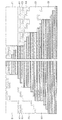
本発明の他の実施形態によれば、連結構造を形成する段階(ステップS2)は第1、第2及び第3パターニング工程を含むことができる。第1〜第3パターニング工程の中のいずれか1つは共通的な単層エッチング方式で実施される1回のエッチング段階(以下、共通的な単層エッチング段階)を含み、第1〜第3パターニング工程の中のその他の1つは選択的な多層エッチング方式で実施される1回のエッチング段階(以下、選択的な多層エッチング段階)を含み、残る1つは共通的な多層エッチング方式で実施される少なくとも1回のエッチング段階(以下、共通的な多層エッチング段階)を含む。
共通的な単層エッチング段階、選択的な多層エッチング段階、及び共通的な多層エッチング段階は、多様に組み合わされて、連結構造を形成するために使用される。例えば、図19に示すように、このような組み合わせの最も単純な形態は、第5〜第10例に開示する方式で具現される。
FIG. 19 is a table showing a method for manufacturing a semiconductor device according to another exemplary embodiment of the present invention.
According to another embodiment of the present invention, forming the connection structure (Step S2) may include first, second and third patterning processes. Any one of the first to third patterning processes includes one etching step (hereinafter referred to as a common single layer etching step) performed by a common single layer etching method. The other one of the patterning processes includes one etching step (hereinafter referred to as a selective multilayer etching step) performed by a selective multilayer etching method, and the other one is performed by a common multilayer etching method. At least one etching step (hereinafter referred to as a common multilayer etching step).
Common single layer etch steps, selective multi-layer etch steps, and common multi-layer etch steps can be used in various combinations to form a connected structure. For example, as shown in FIG. 19, the simplest form of such a combination is implemented by the methods disclosed in the fifth to tenth examples.
説明の重複及び複雑を避けるために、以下では図20〜図29を参照して図19の第5例を例示的に説明する。
図20は、本発明の他の例示的な実施形態の中の1つによる半導体装置の製造方法を説明するためのフローチャートであり、図21〜図24は本発明の他の例示的な実施形態の中の1つによる半導体装置の製造方法を説明するための断面図である。
In order to avoid duplication and complexity of description, the fifth example of FIG. 19 will be described below by way of example with reference to FIGS.
FIG. 20 is a flowchart for explaining a method of manufacturing a semiconductor device according to one of the other exemplary embodiments of the present invention, and FIGS. 21 to 24 are other exemplary embodiments of the present invention. It is sectional drawing for demonstrating the manufacturing method of the semiconductor device by one of these.
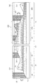
図20及び図21を参照すると、基板10上に水平膜100及び層間絶縁膜200を交互に積層して積層体STを形成した後(ステップS1)、積層体STに対する共通的な単層エッチング段階(第1パターニング工程)(ステップS21)を実施する。
共通的な単層エッチング段階(ステップS21)は互いに離隔された第1エッチング部分E1を形成するように実施する。共通的な単層エッチング段階(ステップS21)は第1及び第2領域R1、R2の全てを露出させる第1マスク211を使用して実施する。これによって、第1エッチング部分E1は、第1及び第2領域R1、R2上に共通的に形成でき、そのエッチング深さは水平膜100の垂直的なピッチであり得る。
Referring to FIGS. 20 and 21, after the
A common single layer etching step (step S21) is performed to form first etched portions E1 that are spaced apart from each other. A common single layer etching step (step S21) is performed using the
図20及び図22を参照すると、第1エッチング部分E1が形成された積層体STに対する選択的な多層エッチング段階(第2パターニング工程)(ステップS22)を実施する。
選択的な多層エッチング段階(ステップS22)は、第1領域R1の一部分を露出させ、第2領域R2及びアレイ領域RAを覆う第2マスク212をエッチングマスクとして使用して実施する。
20 and 22, a selective multilayer etching step (second patterning step) (step S22) is performed on the stacked body ST on which the first etching portion E1 is formed.
The selective multilayer etching step (step S22) is performed using the
例えば、選択的な多層エッチング段階(ステップS22)は、第1領域R1で水平膜100をエッチングする段階を含む。
これによって、第1領域R1上に位置する積層体STに第2エッチング部分E2が局所的に形成される。
第2エッチング部分E2は、水平膜100の垂直的なピッチの2倍に相当するエッチング深さを有するように形成される。選択的な多層エッチング段階(ステップS22)によって、第1及び第2領域R1、R2は、互いに異なる構造を有するようになる。例えば、第1領域R1と第2領域R2との上に位置する積層体STの2つの部分はそれ以上ミラー対称性を有しないようになる。
For example, the selective multilayer etching step (Step S22) includes a step of etching the
As a result, the second etching portion E2 is locally formed in the stacked body ST located on the first region R1.
The second etching portion E2 is formed to have an etching depth corresponding to twice the vertical pitch of the
図20、図23、及び図24を参照すると、第2エッチング部分E2が形成された積層体STに対する共通的な多層エッチング段階(第3パターニング工程)(ステップS23)を実施する。
共通的な多層エッチング段階は、第3マスク213及び第4マスク214を各々エッチングマスクとして使用して実施する第1及び第2共通的な多層エッチング段階を含む。
第3及び第4マスク213、214は、第1及び第2領域R1、R2の一部分を露出させ、アレイ領域RAを覆うように形成される。この実施形態によれば、第4マスク214は第3マスク213より広い幅を有するように形成し、第3マスク213によって隠れる領域を包含することができる。
Referring to FIGS. 20, 23, and 24, a common multilayer etching step (third patterning step) (step S23) is performed on the stacked body ST in which the second etching portion E2 is formed.
The common multilayer etching step includes first and second common multilayer etching steps performed using the
The third and
第1及び第2共通的な多層エッチング段階によって、第1及び第2領域R1、R2の各々には第3及び第4エッチング部分E3、E4が形成される。第3及び第4エッチング部分E3、E4の各々は水平膜100の垂直的なピッチの4倍に該当する深さを有するように形成される。
整理すれば、第1領域R1には第1〜第4エッチング部分(E1、E2、E3、E4)が形成され、第2領域R2には第1、第3、及び第4エッチング部分(E1、E3、E4)が形成される。
Third and fourth etching portions E3 and E4 are formed in the first and second regions R1 and R2, respectively, by the first and second common multi-layer etching steps. Each of the third and fourth etching portions E3 and E4 is formed to have a depth corresponding to four times the vertical pitch of the
In summary, the first to fourth etching portions (E1, E2, E3, E4) are formed in the first region R1, and the first, third, and fourth etching portions (E1, E4) are formed in the second region R2. E3, E4) are formed.
ここで、第1、第3、及び第4エッチング部分(E1、E3、E4)は、それらの各々が形成される水平的位置において互いに段差を有する。
このような水平的位置での段差によって、積層体STは、各階段の高さが水平膜100の垂直的なピッチの複数倍である階段構造を有するように形成される。第2エッチング部分E2が無い場合、積層体STは第1及び第2領域R1、R2でミラー対称的構造を有することができる。
しかし、第1領域R1に形成された第2エッチング部分E2によって、積層体STはそれ以上ミラー対称性を有しない。例えば、積層体STを構成する水平膜100の各々が露出される位置は第1及び第2領域R1、R2で互いに異なる。
Here, the first, third, and fourth etching portions (E1, E3, E4) have a step difference in a horizontal position where each of them is formed.
Due to the level difference at such a horizontal position, the stacked body ST is formed to have a step structure in which the height of each step is a multiple of the vertical pitch of the
However, the stacked body ST has no further mirror symmetry due to the second etching portion E2 formed in the first region R1. For example, the positions where the
図25及び図26は、本発明の他の例示的な実施形態の変形の中の1つによる半導体装置の製造方法を説明するための断面図である。
図25及び図26に示すように、共通的な多層エッチング段階は、第3マスク223及び第4マスク224を各々エッチングマスクとして使用して実施される第1及び第2共通的な多層エッチング段階を含む。
この実施形態によれば、第3マスク223は、第4マスク224より広い幅を有するように形成し、第4マスク224によって隠れる領域を包含することができる。
25 and 26 are cross-sectional views illustrating a method for manufacturing a semiconductor device according to one of the variations of another exemplary embodiment of the present invention.
As shown in FIGS. 25 and 26, the common multilayer etching step includes first and second common multilayer etching steps performed using the
According to this embodiment, the
例えば、第4マスク224は、第3マスク223に対する上述したマスク縮小段階の結果物であり得る。
この場合、第4エッチング部分E4は、第3エッチング部分E3と積層体STの側面との間に位置するエッチング部分を包含することができる。
言い換えれば、共通的な多層エッチング段階が共通的なエッチング方式で実施される複数回のエッチング段階を含む場合、エッチング段階の中で時間的に連続する少なくとも2つの段階は1つのエッチングマスクを共通に使用して実施することができる。
For example, the
In this case, the fourth etching portion E4 can include an etching portion located between the third etching portion E3 and the side surface of the stacked body ST.
In other words, if a common multi-layer etching step includes multiple etching steps performed in a common etching scheme, at least two successive steps in the etching step share one etching mask. Can be implemented using.
例えば、時間的に後行するエッチング段階は時間的に先行するエッチング段階で使用された第3エッチングマスク223の水平的大きさを縮小させる段階を含む。
縮小された第3マスク223は、時間的に後行するエッチング段階で第4マスク224として再使用される。
このようなエッチングマスクの再使用は、誤整列によって起こる技術的難しさ、そして高費用のフォトリソグラフィー工程の回数を減らすことができる。
For example, the temporally subsequent etching step includes reducing the horizontal size of the
The reduced
Such reuse of the etching mask can reduce the technical difficulties caused by misalignment and the number of expensive photolithography steps.
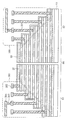
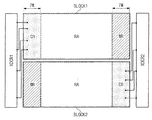
図27は、本発明の他の例示的な実施形態による半導体装置の一部分を示す斜視図である。
本発明の他の例示的な実施形態及びその変形例によれば、図27に示すように、電極ELの中で(4n+1)番目及び(4n+2)番目の電極の各々は第1及び第2領域R1、R2上に各々整列部AP及び連結部CPを有するように形成され、電極ELの中で(4n+3)番目及び(4n+4)番目の電極の各々は第1及び第2領域R2、R1上に各々連結部CP及び整列部APを有するように形成される。
ここで、“n”は(4n+4)が水平膜の総積層数より小さい条件を満足させる“0”又は自然数であり得る。
FIG. 27 is a perspective view illustrating a portion of a semiconductor device according to another exemplary embodiment of the present invention.
According to another exemplary embodiment of the present invention and its modification, as shown in FIG. 27, each of the (4n + 1) th and (4n + 2) th electrodes in the electrode EL has first and second regions. Each of the (4n + 3) th and (4n + 4) th electrodes in the electrode EL is formed on the first and second regions R2 and R1. Each is formed to have a coupling part CP and an alignment part AP.
Here, “n” may be “0” or a natural number that satisfies a condition that (4n + 4) is smaller than the total number of stacked horizontal films.
図28及び図29、は本発明の他の例示的な実施形態及びその変形例による半導体装置の製造方法を説明するための概略的な断面図である。
図28及び図29を参照すると、連結構造を形成する段階は、共通的な単層エッチング段階(ステップS21)を1回実施して第1エッチング部分E1を形成し、選択的な多層エッチング段階(ステップS22)を1回実施して第2エッチング部分E2を形成した後、共通的な多層エッチング段階(ステップS23)を7回実施して第3〜第9エッチング部分(E3、E4、E5、E6、E7、E8、E9)を形成する段階を含む。
28 and 29 are schematic cross-sectional views for explaining a method of manufacturing a semiconductor device according to another exemplary embodiment of the present invention and a modification thereof.
Referring to FIGS. 28 and 29, the connection structure is formed by performing a common single layer etching step (step S21) once to form a first etching portion E1, and a selective multi-layer etching step (step S21). After the step S22) is performed once to form the second etching portion E2, the common multilayer etching step (step S23) is performed seven times to perform the third to ninth etching portions (E3, E4, E5, E6). , E7, E8, E9).
共通的な多層エッチング段階(ステップS23)は互に異なるエッチングマスクを使用して実施する。
例えば、共通的な多層エッチング段階(ステップS23)の各々はそれより先に実施された段階のものより、より増加した幅を有するエッチングマスクを使用して実施する。
この場合、図28に示すように、第3〜第9エッチング部分(E3〜E9)は、順に、それに先に形成されたエッチング部分の下でありながら、積層体STの中心から遠くなる位置に形成される。
The common multilayer etching step (step S23) is performed using different etching masks.
For example, each of the common multi-layer etching steps (step S23) is performed using an etching mask having a larger width than those performed earlier.
In this case, as shown in FIG. 28, the third to ninth etching portions (E3 to E9) are sequentially located below the center of the stacked body ST while being below the etching portion formed earlier. It is formed.
変形された実施形態によれば、共通的な多層エッチング段階(ステップS23)の中の少なくとも1つはそれより先に実施された段階でのものより、より減少した幅を有するエッチングマスクを使用して実施する。
この場合、図29に示すように、第3〜第9エッチング部分(E3〜E9)の中の一部(例えば、E4、E6、E8)はそれより先に形成されたエッチング部分(例えば、E3、E5、E7)より積層体STの中心に近く形成される。
According to a modified embodiment, at least one of the common multi-layer etching steps (step S23) uses an etching mask having a reduced width than that in the earlier performed step. To implement.
In this case, as shown in FIG. 29, some of the third to ninth etching portions (E3 to E9) (for example, E4, E6, and E8) are formed earlier (for example, E3). , E5, E7) closer to the center of the stacked body ST.
図30は、本発明の他の例示的な実施形態の中の他の1つによる半導体装置の製造方法を例示的に説明するための概略的な断面図である。
例えば、図30は、図19に例示的に分類した第10例に該当する製造方法を示すものである。
図19に開示された第10例の場合、連結構造を形成する段階は、共通的な多層エッチング段階(ステップS23)を7回実施して第1〜第7エッチング部分(E1、E2、E3、E4、E5、E6、E7)を形成し、選択的な多層エッチング段階(ステップS22)を1回実施して第8エッチング部分E8を形成し、共通的な単層エッチング段階(ステップS21)を1回実施して第9エッチング部分E9を形成する段階を含む。即ち、共通的な多層エッチング段階(ステップS23)を、共通的な単層エッチング段階(ステップS21)及び選択的な多層エッチング段階(ステップS22)より先に実施することができる。
FIG. 30 is a schematic cross-sectional view for exemplarily explaining a method for manufacturing a semiconductor device according to another embodiment of the present invention.
For example, FIG. 30 shows a manufacturing method corresponding to the tenth example categorized in FIG.
In the case of the tenth example disclosed in FIG. 19, the connection structure is formed by performing a common multilayer etching step (step S23) seven times and performing first to seventh etching portions (E1, E2, E3, E4, E5, E6, E7), the selective multi-layer etching step (step S22) is performed once to form the eighth etching portion E8, and the common single layer etching step (step S21) is 1 Performing the ninth step to form a ninth etching portion E9. That is, the common multilayer etching step (step S23) can be performed before the common single layer etching step (step S21) and the selective multilayer etching step (step S22).
図28〜図30を比較すれば、エッチング段階の順序での相違があるが、積層体STは実質的に同一の模様の階段構造を有する。
言い換えれば、エッチング段階の順序は、製品の開発者の必要によって、多様に変更することができることを意味する。
このような点で、本発明の技術的な思想は、上記例示した又は以下で説明する実施形態に限定されることではなく、上述した実施形態に基づいて多様に変形することができることを意味する。
When comparing FIG. 28 to FIG. 30, there is a difference in the order of the etching steps, but the stacked body ST has a staircase structure having substantially the same pattern.
In other words, the order of the etching steps can be variously changed according to the needs of the product developer.
In this respect, the technical idea of the present invention is not limited to the embodiments illustrated or described below, but can be variously modified based on the above-described embodiments. .
図31は、本発明のその他の例示的な実施形態の中の1つによる半導体装置の製造方法を説明するためのフローチャートであり、図32は本発明のその他の例示的な実施形態の中の1つによる半導体装置の製造方法を説明するためのフローチャート概略的な断面図である。
図31及び図32を参照すると、この実施形態による階段模様の連結構造を形成する工程は、水平膜100を積層して積層体STを形成し(ステップS1)、積層体STに対する第1共通的な単層エッチング段階(ステップS21)、第2共通的な単層エッチング段階(ステップS22)、選択的な多層エッチング段階(ステップS23)、及び共通的な多層エッチング段階(ステップS24)を順次に実施した後、その結果物上に配線構造体300を形成する段階(ステップS3)を含む。
FIG. 31 is a flowchart for explaining a method of manufacturing a semiconductor device according to one of the other exemplary embodiments of the present invention, and FIG. 32 is a flowchart of the method according to the other exemplary embodiment of the present invention. It is a schematic sectional drawing for demonstrating the manufacturing method of the semiconductor device by one.
Referring to FIG. 31 and FIG. 32, the step of forming the staircase pattern connection structure according to this embodiment forms the stacked body ST by stacking the horizontal films 100 (step S1), and the first common to the stacked body ST. A single layer etching step (step S21), a second common single layer etching step (step S22), a selective multilayer etching step (step S23), and a common multilayer etching step (step S24) are sequentially performed. Thereafter, a step (step S3) of forming the
第1共通的な単層エッチング段階(ステップS21)は、互いに離隔された第1エッチング部分E1を形成するように実施する。
第1エッチング部分E1は、第1及び第2領域R1、R2上に共通的に形成され、図32に示すように、第1及び第2領域R1、R2の各々で交互に形成される。
例えば、第1エッチング部分E1は、3Wのピッチを有するように形成し、その各々の幅は2Wである。エッチング深さにおいて、第1エッチング部分E1は水平膜100の垂直的ピッチである。
The first common single layer etching step (step S21) is performed to form first etching portions E1 that are spaced apart from each other.
The first etching portion E1 is formed in common on the first and second regions R1, R2, and is alternately formed in each of the first and second regions R1, R2, as shown in FIG.
For example, the first etching portion E1 is formed to have a pitch of 3W, and each width thereof is 2W. In the etching depth, the first etching portion E1 is a vertical pitch of the
第2共通的な単層エッチング段階(ステップS22)は、互いに離隔された第2エッチング部分E2を形成するように実施する。
第2エッチング部分E2は、第1及び第2領域R1、R2上に共通して形成し、第1エッチング部分E1と同様に、第1及び第2領域R1、R2の各々で交互に形成される。
第2エッチング部分E2は、3Wのピッチを有するように形成し、その各々の幅は1Wである。エッチング深さにおいて、第2エッチング部分E2は水平膜100の垂直的なピッチである。
The second common single layer etching step (step S22) is performed to form second etching portions E2 that are spaced apart from each other.
The second etching portion E2 is formed in common on the first and second regions R1 and R2, and is formed alternately in each of the first and second regions R1 and R2, similarly to the first etching portion E1. .
The second etching portion E2 is formed to have a pitch of 3W, and each width thereof is 1W. The second etching portion E2 is a vertical pitch of the
選択的な多層エッチング段階(ステップS23)は、第2領域R2に局所的に第3エッチング部分R3を形成するように実施する。
図22を参照して説明した実施形態のそれと類似して、第2エッチング部分E2は、水平膜100の垂直的なピッチの2倍に該当するエッチング深さを有するように形成される。選択的な多層エッチング段階(ステップS23)によって、第1及び第2領域R1、R2は互に異なる構造を有するようになる。例えば、第1領域R1と第2領域R2上に位置する積層体STの2つの部分はそれ以上ミラー対称性を有しないようになる。
The selective multilayer etching step (step S23) is performed so as to locally form the third etching portion R3 in the second region R2.
Similar to that of the embodiment described with reference to FIG. 22, the second etching portion E <b> 2 is formed to have an etching depth corresponding to twice the vertical pitch of the
共通的な多層エッチング段階(ステップS24)は、第1及び第2領域R1、R2の両方が積層体STをパターニングするように実施する。
一実施形態によれば、図32に示すように、連結構造の形成工程の間に、共通的な多層エッチング段階(ステップS24)は数回実施し、その段階の各々は互に異なる幅を有するエッチングマスクを使用して実施する。これによって、共通的な多層エッチング段階(ステップS24)によって形成されるエッチング部分(E4、E5、E6)は互いに異なる高さで積層体STの階段模様の構造を定義することができる。
A common multilayer etching step (step S24) is performed such that both the first and second regions R1, R2 pattern the stack ST.
According to one embodiment, as shown in FIG. 32, during the connection structure forming process, the common multilayer etching step (step S24) is performed several times, each of which has a different width from each other. This is performed using an etching mask. Thus, the etched portions (E4, E5, E6) formed by the common multilayer etching step (step S24) can define the staircase pattern structure of the stacked body ST at different heights.
配線構造体300を形成する段階(ステップS3)は、図8を参照して説明した実施形態のそれと実質的に同一の方式で実施する。
積層体STは、第1及び第2領域R1、R2の各々に形成されて配線構造体300への電気的な接続として使用される複数の階段形態の領域を包含する。
図31及び図32を参照して説明した上記の実施形態によれば、階段形態の領域の各々は連続的に積層された4層の水平膜100によって構成される。
The step of forming the wiring structure 300 (step S3) is performed in substantially the same manner as that of the embodiment described with reference to FIG.
The stacked body ST includes a plurality of staircase-shaped regions formed in each of the first and second regions R1 and R2 and used as an electrical connection to the
According to the above-described embodiment described with reference to FIGS. 31 and 32, each of the staircase-shaped regions is constituted by the four layers of the
先の実施形態の場合、階段形態の領域の各々は連続的に積層された1層又は2層の水平膜100によって構成される。即ち、階段形態の領域の各々の垂直的厚さ(即ち、これを構成する水平膜の個数)は特定の数値に限定されることではなく、図31及び図32によって例示的に示したように、製品の開発者の必要によって、多様に変化され得る。
例えば、階段形態の領域の各々を構成する水平膜100の積層数は、2〜16の中の少なくとも1つであり得る。
In the case of the previous embodiment, each of the staircase-shaped regions is constituted by one or two layers of
For example, the number of stacked
図33〜図37は、本発明のその他の例示的な実施形態による半導体装置の製造方法を説明するための概略的な断面図である。
例えば、図33〜図37は、図31及び図32を参照して説明した実施形態の可能である変形の中の一部を例示的に示す。
たとえ重複を避けるために別の説明が提供しなくとも、ここで説明する方法的及び構造的な特徴は、上述した又は後述する本発明の他の実施形態でも同一又は類似の方式が適用又は具現される。また、説明を簡単にするために、先に説明したものと同一の構成要素又は技術的な特徴に対する重複される説明は省略する。
33 to 37 are schematic cross-sectional views for explaining a method of manufacturing a semiconductor device according to another exemplary embodiment of the present invention.
For example, FIGS. 33-37 exemplarily illustrate some of the possible variations of the embodiment described with reference to FIGS.
The methodic and structural features described herein may be applied or implemented in the same or similar ways in other embodiments of the invention described above or described below, even if no separate description is provided to avoid duplication. Is done. In addition, for the sake of simplicity, redundant description of the same components or technical features as those described above will be omitted.
一実施形態によれば、図32を参照して説明した実施形態は、選択的な多層エッチング段階を共通的な多層エッチング段階の間に実施するように変形される。
例えば、選択的な多層エッチング段階は、第1及び第2共通的な単層エッチング段階及び共通的な多層エッチング段階の以後に実施し、図33に示すように、水平膜100の垂直的なピッチの2倍に相当するエッチング深さを有する第4エッチング部分E4を形成する。
According to one embodiment, the embodiment described with reference to FIG. 32 is modified to perform selective multilayer etching steps during a common multilayer etching step.
For example, the selective multi-layer etching step is performed after the first and second common single-layer etching steps and the common multi-layer etching step, and the vertical pitch of the
以後、積層体STは、共通的な多層エッチング方式で追加的にパターニングされ得る。
この実施形態による第1及び第2共通的な単層エッチング段階、選択的な多層エッチング段階、共通的な多層エッチング段階は、図32を参照して説明した実施形態のそれらと同一の方式で実施することができる。
積層体STの最終構造は、図32及び図33を参照して説明した実施形態の間で差がない。これは工程順序での変化又は選択的な多層エッチング段階の実施順序での変化にもかかわらず、同一の模様の階段構造を具現することができることを意味する。
Thereafter, the stacked body ST can be additionally patterned by a common multilayer etching method.
The first and second common single layer etching steps, the selective multilayer etching step, and the common multilayer etching step according to this embodiment are performed in the same manner as those of the embodiment described with reference to FIG. can do.
The final structure of the stacked body ST is not different between the embodiments described with reference to FIGS. 32 and 33. This means that a stepped structure with the same pattern can be realized regardless of changes in the process order or the execution order of the selective multilayer etching steps.
一実施形態によれば、図32を参照して説明した実施形態は、選択的な多層エッチング段階を第1及び第2共通的な単層エッチング段階の以前に実施するように変形される。
例えば、選択的な多層エッチング段階によって形成される第4エッチング部分E4は、図34に示すように、水平膜100の垂直的なピッチの2倍に相当するエッチング深さを有しながら、積層体STの最上部領域に形成される。
According to one embodiment, the embodiment described with reference to FIG. 32 is modified to perform the selective multi-layer etch step prior to the first and second common single layer etch steps.
For example, the fourth etching portion E4 formed by the selective multilayer etching step has an etching depth corresponding to twice the vertical pitch of the
以後、積層体STに対する共通的な多層エッチング段階を数回実施する。
この実施形態による第1及び第2共通的な単層エッチング段階、選択的な多層エッチング段階、共通的な多層エッチング段階は、図32を参照して説明した実施形態のそれらと同一の方式で実施することができる。
積層体STの最終構造は、図32及び図34を参照して説明した実施形態の間で差がない。図33の実施形態と同様に、これは工程順序での変化又は選択的な多層エッチング段階の実施順序での変化にもかかわらず、同一の模様の階段構造を具現することができることを意味する。
Thereafter, the common multilayer etching step for the stacked body ST is performed several times.
The first and second common single layer etching steps, the selective multilayer etching step, and the common multilayer etching step according to this embodiment are performed in the same manner as those of the embodiment described with reference to FIG. can do.
The final structure of the stacked body ST is not different between the embodiments described with reference to FIGS. 32 and 34. Similar to the embodiment of FIG. 33, this means that a stepped structure with the same pattern can be implemented despite changes in the process order or changes in the order of execution of the selective multilayer etching steps.
一実施形態によれば、図32を参照して説明した実施形態は、共通的な多層エッチング段階の中の1つを第1及び第2共通的な単層エッチング段階の以前に実施するように変形される。
例えば、共通的な多層エッチング段階によって形成される第1エッチング部分E1は、図35に示すように、水平膜100の垂直的なピッチの6倍に該当するエッチング深さを有しながら、積層体STの最上部領域に形成される。
According to one embodiment, the embodiment described with reference to FIG. 32 is such that one of the common multilayer etch steps is performed before the first and second common single layer etch steps. Deformed.
For example, the first etching portion E1 formed by the common multi-layer etching step has an etching depth corresponding to 6 times the vertical pitch of the
以後、第1及び第2共通的な単層エッチング段階、選択的な多層エッチング段階、共通的な多層エッチング段階が順次に積層体STに対して実施され、これらの各々は図32を参照して説明した実施形態のそれらと同一の方式で実施することができる。
積層体STの最終構造は、図32及び図35を参照して説明した実施形態の間で差がない。図33及び図34の実施形態と同様に、これは工程順序での変化又は選択的な多層エッチング段階の実施順序での変化にもかかわらず、同一の模様の階段構造を具現することができることを意味する。
Thereafter, the first and second common single-layer etching steps, the selective multi-layer etching step, and the common multi-layer etching step are sequentially performed on the stacked body ST, each of which is illustrated in FIG. It can be implemented in the same manner as those of the described embodiments.
The final structure of the stacked body ST is not different between the embodiments described with reference to FIGS. 32 and 35. Similar to the embodiment of FIGS. 33 and 34, it is possible to implement a step structure with the same pattern, regardless of a change in the process order or a change in the execution order of the selective multilayer etching steps. means.
一実施形態によれば、図35を参照して説明した実施形態と比較する時、共通的な多層エッチング段階の中の少なくとも1つはエッチング領域で変化するように変形される。
例えば、図36の実施形態によれば、図35の第1及び第6エッチング部分E1、E6を形成するために使用されるエッチングマスクは互いに変更することができる。この場合にも、図36に示すように、積層体STは、図32〜図35を参照して説明した実施形態と同一である最終構造を有することができる。これは、共通的な多層エッチング段階の実施順序が変わる場合にも、同一の模様の階段構造を具現することができることを意味する。
According to one embodiment, when compared to the embodiment described with reference to FIG. 35, at least one of the common multilayer etching steps is modified to vary in the etched region.
For example, according to the embodiment of FIG. 36, the etching masks used to form the first and sixth etching portions E1, E6 of FIG. 35 can be changed from each other. Also in this case, as shown in FIG. 36, the stacked body ST can have a final structure that is the same as the embodiment described with reference to FIGS. 32 to 35. This means that a stepped structure having the same pattern can be realized even when the execution order of the common multi-layer etching step is changed.
図32を参照して説明した実施形態は、上述した他の実施形態の中のいずれか1つ(例えば、図17を参照して説明した実施形態)と組み合わされて、階段構造の連結領域を形成する。
例えば、図37に例示的に示すように、選択的なエッチング段階、第1共通的な単層エッチング段階、第2共通的な単層エッチング段階、及び複数回の共通的な多層エッチング段階を順次に実施することによって、積層体STは階段構造を有するように形成される。
The embodiment described with reference to FIG. 32 is combined with any one of the other embodiments described above (for example, the embodiment described with reference to FIG. 17) to provide a connection region of the staircase structure. Form.
For example, as shown in FIG. 37, a selective etching step, a first common single layer etching step, a second common single layer etching step, and a plurality of common multilayer etching steps are sequentially performed. As a result, the stacked body ST is formed to have a staircase structure.
共通的な多層エッチング段階は、水平膜100の垂直的なピッチの3倍に該当するエッチング深さを有するエッチング部分(E4、E5、E6)を各々形成するように実施する。第1及び第2共通的な単層エッチング段階は、図32を参照して説明した実施形態のそれらと同一の方式で実施することができる。
実施形態のこのような組み合わせは、図37に例示的に示した方法に限定されることではなく、上述した又は後述する本発明の他の実施形態でも同一又は類似な方式で適用又は具現され得る。
A common multi-layer etching step is performed to form etching portions (E4, E5, E6) each having an etching depth corresponding to three times the vertical pitch of the
Such a combination of the embodiments is not limited to the method exemplarily shown in FIG. 37, and may be applied or implemented in the same or similar manner in other embodiments of the present invention described above or described below. .
図38は、本発明のその他の実施形態による半導体装置の製造方法を説明するためのフローチャートである。
図39〜図43は、本発明のその他の実施形態による半導体装置の製造方法を説明するための断面図である。
説明を簡単にするために、先に説明したことと同一の構成要素又は技術的な特徴に対する重複する説明は省略する。また、ここで説明する方法及び構造的な特徴は、上述した又は後述する本発明の他の実施形態でも同一又は類似な方式で適用又は具現され得る。
FIG. 38 is a flowchart for explaining a method of manufacturing a semiconductor device according to another embodiment of the present invention.
39 to 43 are cross-sectional views for explaining a method of manufacturing a semiconductor device according to another embodiment of the present invention.
In order to simplify the description, duplicate descriptions for the same components or technical features as those described above are omitted. Also, the method and structural features described herein may be applied or implemented in the same or similar manner in other embodiments of the invention described above or described below.
図38及び図39を参照すると、この実施形態によれば、基板10は互いに離隔された第1、第2及び第3領域(D1、D2、D3)を含む。
基板10上に水平膜100及び層間絶縁膜200を交互に積層して積層体STを形成した後(ステップS1)、積層体STに対する第1多層エッチング段階(ステップS21)を実施する。
一実施形態によれば、第1多層エッチング段階(ステップS21)は、第2及び第3領域D2、D3を露出させる第1エッチングマスク241を使用して積層体STを異方的にエッチングする段階を含む。これによって、第2及び第3領域D2、D3を含む領域に、第1エッチング部分E1が形成される。
38 and 39, according to this embodiment, the
After the
According to one embodiment, the first multilayer etching step (step S21) anisotropically etches the stacked body ST using the
図38及び図40を参照すると、積層体STに対する第2多層エッチング段階(ステップS22)を実施する。
第2多層エッチング段階(ステップS22)は、第3領域D3を局所的に露出させる第2エッチングマスク242を使用して積層体STを異方的にエッチングする段階を含む。
これによって、第3領域D3を含む領域に、第2エッチング部分E2が形成される。第1及び第2エッチング部分E1、E2の深さは実質的に同一であるが、これに限定されることではない。
Referring to FIGS. 38 and 40, the second multilayer etching step (Step S22) is performed on the stacked body ST.
The second multilayer etching step (step S22) includes a step of anisotropically etching the stacked body ST using the
As a result, the second etching portion E2 is formed in the region including the third region D3. The depths of the first and second etching portions E1 and E2 are substantially the same, but are not limited thereto.
図38及び図41を参照すると、第2多層エッチング段階(ステップS22)が実施された結果物上に、第3エッチングマスク243を形成する。
第3エッチングマスク243は第1〜第3領域(D1、D2、D3)の各々を部分的に露出させる開口部OPを有するように形成される。
Referring to FIGS. 38 and 41, a
The
図38及び図42を参照すると、積層体STに対する共通的な単層エッチング段階(ステップS21)を複数回実施する。
共通的な単層エッチング段階(ステップS21)は、第3エッチングマスク243を共通に使用して実施する。
共通的な単層エッチング段階(ステップS21)を実施する間に、上述したマスク縮小段階が第3エッチングマスク243に対して実施する。これによって、共通的な単層エッチング段階(ステップS21)が進行するほど、積層体STのエッチングされる部分の幅は増加する。その結果、第1〜第3領域(D1、D2、D3)には下方にテーパーされた断面を有する第3エッチング部分E3が形成される。
Referring to FIGS. 38 and 42, a common single layer etching step (step S21) for the stacked body ST is performed a plurality of times.
The common single layer etching step (step S21) is performed using the
The mask reduction step described above is performed on the
図38及び図43を参照すると、第1〜第3エッチング部分(E1〜E3)を満たす第1層間絶縁膜251を形成する。
第1層間絶縁膜251は、平坦化エッチング工程(例えば、化学的機械的研磨工程)を通じて平坦な上部面を有するように形成される。
以後、第2層間絶縁膜252を形成し、第2層間絶縁膜252及び第1層間絶縁膜251を貫通するプラグ301を形成する。一実施形態によれば、上述したように、プラグ301を形成する前に、水平膜100を金属を含む物質で代替する工程をさらに実施することができる。
38 and 43, a first
The first
Thereafter, a second
上述した実施形態によれば、第1〜第3領域(D1、D2、D3)の間には、第1及び第2ダミー領域DR1、DR2が介在し、第1及び第2ダミー領域DR1、DR2の上にはダミーパターンDPが形成される。
ダミーパターンDPの各々は、図44に示すように、共通的な単層エッチング段階(ステップS23)によって形成される第1側面SS1と第1又は第2多層エッチング段階(ステップS21、ステップS22)によって形成される第2側面SS2を有する。
第1側面及び階段形態の連結構造は、第3エッチング部分E3の互いに対向する側面であり得る。これによって、第1側面SS1は、第1〜第3領域(D1、D2、D3)に形成される階段形態の連結構造に対してミラー対称的な断面形状を有するように形成される。
According to the embodiment described above, the first and second dummy regions DR1, DR2 are interposed between the first to third regions (D1, D2, D3), and the first and second dummy regions DR1, DR2 are interposed. A dummy pattern DP is formed on the top.
As shown in FIG. 44, each dummy pattern DP is formed by a first side surface SS1 formed by a common single layer etching step (step S23) and a first or second multilayer etching step (steps S21 and S22). It has the 2nd side surface SS2 formed.
The connection structure of the first side surface and the staircase form may be the side surfaces of the third etching portion E3 facing each other. Accordingly, the first side surface SS1 is formed to have a mirror-symmetric cross-sectional shape with respect to the step-shaped connection structure formed in the first to third regions (D1, D2, D3).
これとは異なり、第2側面SS2は、第1又は第2多層エッチング段階(ステップS21、ステップS22)によって形成され、第1側面SS1と異なる断面形状を有することができる。
例えば、第1側面SS1はA1の傾斜角を有するように形成され、第2側面SS2はA1とは異なるA2の傾斜角を有するように形成され得る。
一実施形態で、第2側面SS2の傾斜角A2は、0°〜45°であり得る。
In contrast, the second side surface SS2 may be formed by the first or second multilayer etching step (Step S21, Step S22) and have a different cross-sectional shape from the first side surface SS1.
For example, the first side surface SS1 may be formed to have an inclination angle of A1, and the second side surface SS2 may be formed to have an inclination angle of A2 different from A1.
In one embodiment, the inclination angle A2 of the second side surface SS2 may be 0 ° to 45 °.
一実施形態で、第1及び第2多層エッチング段階(ステップS21、ステップS22)の中のいずれか1つはマスク縮小方式で実施される複数の多層エッチング段階を含む。
この場合、図44に示すように、第2側面SS2は、階段形態の断面形状を有し得、その傾斜角A2は、0°より大きくなり得る。
ダミーパターンDPの第2側面SS2がこのように傾いた側面を有する場合、第2又は第3エッチングマスク242、243の薄膜化及びこれに伴う工程不良を防止できる。
In one embodiment, any one of the first and second multilayer etching steps (step S21, step S22) includes a plurality of multilayer etching steps performed in a mask reduction scheme.
In this case, as shown in FIG. 44, the second side surface SS2 may have a step-like cross-sectional shape, and the inclination angle A2 may be greater than 0 °.
When the second side surface SS2 of the dummy pattern DP has the inclined side surface, it is possible to prevent the second or
ダミーパターンDPの存在によって、積層体STの高さはその縁部で急激に変わらない。これは第1又は第2層間絶縁膜251、252の蒸着プロフィールを改善することをできる。
これに加えて、ダミーパターンDPの存在によって、第1層間絶縁膜251に対する平坦化エッチング工程で積層体STの縁部が損傷される技術的難しさを防止できる。
Due to the presence of the dummy pattern DP, the height of the stacked body ST does not change abruptly at the edge thereof. This can improve the deposition profile of the first or second
In addition, the presence of the dummy pattern DP can prevent technical difficulty that the edge of the stacked body ST is damaged in the planarization etching process for the first
図45及び図46は、図39〜図43を参照して先に説明した実施形態の変形を説明するための概略的な断面図である。
図39〜図43を参照して説明した実施形態によれば、階段模様の連結構造がアレイ領域RAの一側に形成される。しかし、図39〜図43を参照して説明した実施形態は、階段模様の連結構造をアレイ領域RAの両側に形成するように変形され得る。
45 and 46 are schematic cross-sectional views for explaining a modification of the embodiment described above with reference to FIGS. 39 to 43.
According to the embodiment described with reference to FIGS. 39 to 43, the staircase pattern connection structure is formed on one side of the array region RA. However, the embodiment described with reference to FIGS. 39 to 43 may be modified to form a staircase-shaped connection structure on both sides of the array region RA.
例えば、プラグ301と連結される積層体STの階段形領域を、基板10の上部面との離隔距離にしたがって、第1〜第4連結領域(D1、D2、D3、D4)であるとすれば、第1〜第4連結領域(D1、D2、D3、D4)の一部は、アレイ領域RAの一側(例えば、第1領域R1)に形成され、残りはアレイ領域RAの他側(例えば、第2領域R2)に形成される。
For example, if the stepped region of the stacked body ST connected to the
図45に示す実施形態によれば、第2及び第4連結領域D2、D4が第1領域R1に形成され、第1及び第3連結領域D1、D3が第2領域D2に形成される。
一実施形態で、第2及び第4連結領域D2、D4の間、又は第1及び第3連結領域D1、D3の間隔「H」は。これらの間に位置する連結領域の厚さと実質的に同一であり得る。
According to the embodiment shown in FIG. 45, the second and fourth connection regions D2 and D4 are formed in the first region R1, and the first and third connection regions D1 and D3 are formed in the second region D2.
In one embodiment, the distance “H” between the second and fourth connection regions D2 and D4 or between the first and third connection regions D1 and D3. It may be substantially the same as the thickness of the connecting region located between them.
図46に示す実施形態によれば、第1及び第2連結領域D1、D2が第1領域R1に形成され、第3及び第4連結領域D3、D4が第2領域D2に形成される。 According to the embodiment shown in FIG. 46, the first and second connection regions D1 and D2 are formed in the first region R1, and the third and fourth connection regions D3 and D4 are formed in the second region D2.
図47及び図48は、本発明のその他の例示的な実施形態による半導体装置を説明するための概略的な断面図である。
説明を簡単にするために、先に説明したことと同一の構成要素又は技術的な特徴に対する重複する説明は省略する。また、ここで説明する方法及び構造的な特徴は、上述した又は後述する本発明の他の実施形態でも同一又は類似な方式で適用又は具現され得る。
47 and 48 are schematic cross-sectional views for explaining a semiconductor device according to another exemplary embodiment of the present invention.
In order to simplify the description, duplicate descriptions for the same components or technical features as those described above are omitted. Also, the method and structural features described herein may be applied or implemented in the same or similar manner in other embodiments of the invention described above or described below.
上述した又は後述する本発明の他の実施形態は、図44を参照して説明した技術的な特徴の一部を含むように具現される。
例えば、図17を参照して説明した段階で、第1エッチング部分E1の側壁は、図44の第2側面SS2が有する技術的な特徴を含むように形成される。言い換えれば、図47に示すように、第1エッチング部分E1の側壁は、基板10の上部面の法線に対して傾いた断面形状を有するように形成される。また、第1エッチング部分E1の側壁は、マスク縮小方式で実施される複数の多層エッチング段階を通じて形成でき、この場合、図47に示すように、第1エッチング部分E1の側壁は、階段形態の断面形状を有する。
Other embodiments of the present invention described above or described below are implemented to include some of the technical features described with reference to FIG.
For example, at the stage described with reference to FIG. 17, the side wall of the first etching portion E1 is formed to include the technical features of the second side surface SS2 of FIG. In other words, as shown in FIG. 47, the side wall of the first etching portion E1 is formed to have a cross-sectional shape inclined with respect to the normal line of the upper surface of the
他の例として、図37の実施形態で、第1エッチング部分E1の側壁は、基板10の上部面の法線に対して傾いた断面形状を有するように形成される。
また、第1エッチング部分E1の側壁は、マスク縮小方式で実施される複数の多層エッチング段階を通じて形成でき、この場合、図48に示すように、第1エッチング部分E1の側壁は、階段形態の断面形状を有することができる。
As another example, in the embodiment of FIG. 37, the side wall of the first etching portion E1 is formed to have a cross-sectional shape inclined with respect to the normal line of the upper surface of the
In addition, the sidewall of the first etching portion E1 can be formed through a plurality of multilayer etching steps performed in a mask reduction method. In this case, as shown in FIG. 48, the sidewall of the first etching portion E1 has a stepped cross section. Can have a shape.
図49〜図51は、本発明のその他の例示的な実施形態による半導体装置の製造方法を説明するための断面図であり、図52は本発明のその他の例示的な実施形態による半導体装置の一部分を示す斜視図である。
説明を簡単にするために、先に説明したことと同一の構成要素又は技術的な特徴に対する重複する説明は省略する。また、ここで説明する方法及び構造的な特徴は、上述した又は後述する本発明の他の実施形態でも同一又は類似な方式で適用又は具現され得る。
49 to 51 are cross-sectional views for explaining a method of manufacturing a semiconductor device according to another exemplary embodiment of the present invention. FIG. 52 is a cross-sectional view of a semiconductor device according to another exemplary embodiment of the present invention. It is a perspective view which shows a part.
In order to simplify the description, duplicate descriptions for the same components or technical features as those described above are omitted. Also, the method and structural features described herein may be applied or implemented in the same or similar manner in other embodiments of the invention described above or described below.
図49を参照すると、共通的な単層エッチング段階(S21)によって形成される第1エッチング部分E1は、これらの間に残存する積層体STの部分STRより狭い幅を有するように形成される。例えば、図49に示すように、第1エッチング部分E1の各々の幅は「b」であり、積層体STの部分STRの各々の幅は、「b」より大きい、「a」であり得る。 Referring to FIG. 49, the first etching portion E1 formed by the common single layer etching step (S21) is formed to have a narrower width than the portion STR of the stacked body ST remaining between them. For example, as shown in FIG. 49, the width of each of the first etching portions E1 may be “b”, and the width of each of the portions STR of the stacked body ST may be “a”, which is larger than “b”.
図50及び図51を参照すると、共通的な多層エッチング段階(ステップS23)は積層体STの中心部分から水平に離隔された残存部RPを形成するように実施する。
例えば、共通的な多層エッチング段階(ステップS23)によって形成される第2〜第4エッチング部分(E2〜E4)によって、残存部RPは積層体STの本体から水平に分離され得る。この場合、図52に示すように、プラグ301の周囲には残存部RPが存在する。
Referring to FIGS. 50 and 51, the common multilayer etching step (step S23) is performed so as to form a remaining portion RP that is horizontally separated from the central portion of the stacked body ST.
For example, the remaining portion RP can be horizontally separated from the main body of the stacked body ST by the second to fourth etching portions (E2 to E4) formed by the common multilayer etching step (step S23). In this case, as shown in FIG. 52, there is a remaining portion RP around the
誤整列が無い場合、残存部RPの幅は、積層体STの部分STRの幅と第1エッチング部分E1の幅との差(即ち、a−b)であり得る。一実施形態によれば、図52の残存部RPは、同一の高さに形成される電極ELと同一である物質で形成でき、他の導電性要素(例えば、電極EL又はプラグ301から離隔されて電気的にフローティング状態にあり得る)。 When there is no misalignment, the width of the remaining portion RP may be a difference (that is, a−b) between the width of the portion STR of the stacked body ST and the width of the first etching portion E1. According to one embodiment, the remaining portion RP of FIG. 52 may be formed of the same material as the electrode EL formed at the same height, and is separated from other conductive elements (eg, the electrode EL or the plug 301). Can be electrically floating).
図53は、図49〜図51を参照して説明した実施形態との比較のために提供する断面図である。
図23を参照して説明した共通的な多層エッチング段階(ステップS23)で誤整列Mが発生する場合、図53に示すように、連結部CPが第3エッチング部分E3によって積層体STの中心部分から分離される。連結部CPのこのような分離は半導体装置での電気的な断線不良を生じさせる。反面、図49〜図51を参照して説明したように、積層体STの部分STRが第1エッチング部分E1より広い幅を有するように形成される場合、誤整列Mに対する工程マージンを確保することができ、その結果、誤整列Mと関連した技術的な問題(例えば、電気的な断線不良)は減少される。
53 is a cross-sectional view provided for comparison with the embodiment described with reference to FIGS. 49 to 51.
When misalignment M occurs in the common multi-layer etching step (step S23) described with reference to FIG. 23, as shown in FIG. 53, the connecting portion CP is formed in the central portion of the stacked body ST by the third etching portion E3. Separated from. Such separation of the connecting portion CP causes an electrical disconnection failure in the semiconductor device. On the other hand, as described with reference to FIGS. 49 to 51, when the portion STR of the stacked body ST is formed to have a wider width than the first etching portion E1, a process margin for misalignment M is ensured. As a result, technical problems associated with misalignment M (eg, poor electrical disconnection) are reduced.
図54及び図55は、各々、本発明の一実施形態と比較例による半導体装置の階段式構造間の比較を説明するための概略的な断面図である。
比較例による半導体装置は、選択的なエッチング方式及び/又は多層エッチング方式が適用されないパターニング工程を通じて形成される。即ち、比較例による半導体装置は単なる共通的な単層エッチング方式で進行される複数のエッチング段階を通じて形成される。この場合、本発明の一実施形態による半導体装置は図54に示す第1階段式構造ST1を有するように形成され、比較例による半導体装置は図55に示す第2階段式構造ST2を有するように形成される。
54 and 55 are schematic cross-sectional views for explaining comparison between the stepped structure of the semiconductor device according to the embodiment of the present invention and the comparative example, respectively.
The semiconductor device according to the comparative example is formed through a patterning process to which a selective etching method and / or a multilayer etching method is not applied. That is, the semiconductor device according to the comparative example is formed through a plurality of etching steps that are performed by a simple single-layer etching method. In this case, the semiconductor device according to the embodiment of the present invention is formed to have the first stepped structure ST1 shown in FIG. 54, and the semiconductor device according to the comparative example has the second stepped structure ST2 shown in FIG. It is formed.
図54及び図55を参照すると、本発明の実施形態の場合、上述した多層エッチング方式のパターニング工程が使用された結果として、第1階段式構造ST1の階段高さは水平膜100の垂直的なピッチPの2倍又はその以上であり得る。
これとは異なり、比較例の場合、単層エッチング方式のパターニング工程が使用されるので、第2階段式構造ST2の階段高さは、全部水平膜100の垂直的なピッチPであり得る。
Referring to FIGS. 54 and 55, in the embodiment of the present invention, the step height of the first step structure ST1 is vertical to the
In contrast, in the case of the comparative example, since the patterning process of the single layer etching method is used, the step height of the second step structure ST2 can be the vertical pitch P of the
即ち、第1階段式構造ST1は、第2階段式構造ST2に比べて増加した階段高さを有する。このような階段高さの増加は、階段領域の幅の減少をもたらすことができる。
例えば、第1階段式構造ST1の階段領域が、図54に例示的に示すように3Wの幅を有すれば、第2階段式構造ST2の階段領域は、図55に例示的に示すように7Wの幅を有する。即ち、階段式構造の占有面積を半分又はその以上に減らし得る。
That is, the first staircase structure ST1 has an increased staircase height compared to the second staircase structure ST2. Such an increase in the staircase height can result in a decrease in the width of the staircase region.
For example, if the staircase region of the first staircase structure ST1 has a width of 3 W as illustrated in FIG. 54, the staircase region of the second staircase structure ST2 is as illustrated in FIG. It has a width of 7W. That is, the area occupied by the stepped structure can be reduced to half or more.
これに加えて、上述した製造方法によれば、図54に示す第1階段式構造ST1は、多層エッチング方式で実施される3回のエッチング段階(ES1、ES2、ES3)及び単層エッチング方式で実施される1回のエッチング段階ES4を通じて形成される。
これとは異なり、上述した比較例の方法によれば、すべての水平膜100が単層エッチングの方式にパターニングされるので、第2階段式構造ST2は、7回のエッチング段階(CES1〜CES7)を通じて形成される。
即ち、本発明の実施形態による半導体装置は上述した比較例による半導体装置に比べて減少した工程段階を通じて製造される。このような工程単純化は、製造費用及び工程不良を減らすことができる。
In addition, according to the manufacturing method described above, the first staircase structure ST1 shown in FIG. 54 has three etching steps (ES1, ES2, ES3) performed by a multilayer etching method and a single layer etching method. It is formed through one etching step ES4 to be performed.
In contrast, according to the method of the comparative example described above, since all the
That is, the semiconductor device according to the embodiment of the present invention is manufactured through reduced process steps as compared with the semiconductor device according to the comparative example described above. Such process simplification can reduce manufacturing costs and process failures.
図56及び図57は、各々、本発明の一実施形態と比較例による半導体装置間の技術的相違点を説明するための図である。
図56及び図57を参照すると、半導体装置は、3次元的に配列されたメモリセルが提供される第1及び第2ブロック(BLOCK1、BLOCK2)及びこれらの周囲に配置される複数のX−デコーダーを含むことができる。
56 and 57 are diagrams for explaining technical differences between the semiconductor device according to the embodiment of the present invention and the comparative example, respectively.
Referring to FIGS. 56 and 57, the semiconductor device includes first and second blocks (BLOCK1, BLOCK2) provided with three-dimensionally arranged memory cells and a plurality of X-decoders arranged around these blocks. Can be included.
本発明の実施形態によれば、図56に示すように、第1及び第2ブロック(BLOCK1、BLOCK2)の各々は、アレイ領域RA及びその両側に配置される第1領域R1及び第2領域R2を含み、X−デコーダーは第1ブロックBLOCK1の第1及び第2領域R1、R2の各々に隣接する第1及び第2X−デコーダー(XDCR1、XDCR2)を含むことができ、第2ブロックBLOCK2の第1及び第2領域R1、R2の各々に隣接する第3及び第4X−デコーダー(XDCR3、XDCR4)を含むことができる。 According to the embodiment of the present invention, as shown in FIG. 56, each of the first and second blocks (BLOCK1, BLOCK2) includes an array region RA and a first region R1 and a second region R2 disposed on both sides thereof. The X-decoder may include first and second X-decoders (XDCR1, XDCR2) adjacent to the first and second regions R1 and R2 of the first block BLOCK1, and the second block BLOCK2 includes a first block BLOCK2. Third and fourth X-decoders (XDCR3, XDCR4) adjacent to each of the first and second regions R1 and R2 may be included.
比較例によれば、図57に示すように、第1及び第2ブロック(BLOCK1、BLOCK2)の各々はアレイ領域RA及びその両側に配置される連結領域CR及び無駄になる領域WRを含み、X−デコーダーは、第1及び第2ブロック(BLOCK1、BLOCK2)の連結領域CRに各々隣接する第1及び第2X−デコーダー(XDCR1、XDCR2)を含むことができる。 According to the comparative example, as shown in FIG. 57, each of the first and second blocks (BLOCK1, BLOCK2) includes an array region RA, a connection region CR disposed on both sides thereof, and a waste region WR, The decoder may include first and second X-decoders (XDCR1, XDCR2) adjacent to the connection region CR of the first and second blocks (BLOCK1, BLOCK2), respectively.
比較例の場合、X−デコーダーは、連結領域CRを通じてアレイ領域RAに配置されたメモリセルへ接続することができる。反面、無駄になる領域WRは上述した比較例による半導体装置が共通的なエッチング方式のエッチング段階を通じて形成されるので、作られた結果物であるが、第1及び第2X−デコーダー(XDCR1、XDCR2)と水平膜100又は電極ELとの間の電気的な接続のために使用されない。
これとは異なり、本発明の実施形態によれば、第1及び第2ブロック(BLOCK1、BLOCK2)の第1及び第2領域R1、R2は全て第1〜第4X−デコーダー(XDCR1〜XDCR4)と水平膜100又は電極ELとの間の電気的な接続のために使用される。
In the case of the comparative example, the X-decoder can be connected to the memory cells arranged in the array region RA through the connection region CR. On the other hand, the wasted region WR is a resultant product because the semiconductor device according to the above-described comparative example is formed through a common etching method etching step, but the first and second X-decoders (XDCR1, XDCR2). ) And the
In contrast, according to the embodiment of the present invention, the first and second regions R1 and R2 of the first and second blocks (BLOCK1 and BLOCK2) are all the first to fourth X-decoders (XDCR1 to XDCR4). Used for electrical connection between
図54及び図55を参照して説明した階段式構造の占有面積での減少によって、本発明の実施形態による第1及び第2領域R1、R2の各々の幅は、比較例の連結領域CR及び無駄になる領域WRの幅より小さいことがあり得る。
例えば、図56及び図57に示すように、第1及び第2領域R1、R2の各々は3Wの幅を有し、連結領域CR及び無駄になる領域WRは7Wの幅を有する。
Due to the reduction in the occupied area of the stepped structure described with reference to FIGS. 54 and 55, the width of each of the first and second regions R1 and R2 according to the embodiment of the present invention is changed to the connection region CR and the comparative example. It may be smaller than the width of the wasted area WR.
For example, as shown in FIGS. 56 and 57, each of the first and second regions R1 and R2 has a width of 3W, and the connection region CR and the wasted region WR have a width of 7W.
即ち、比較例の場合、無駄になる領域WRは電気的な接続のために使用されないだけでなく、第1及び第2領域R1、R2に比べて大きい占有面積を有する。
無駄になる領域WRの存在及びその大きい占有面積を考慮する時、本発明の実施形態による半導体装置は、比較例による半導体装置に比べて増加した集積度又は増加したメモリ容量を有することができる。
That is, in the comparative example, the wasted region WR is not used for electrical connection, but has a larger occupied area than the first and second regions R1 and R2.
When considering the existence of the wasted region WR and its large occupied area, the semiconductor device according to the embodiment of the present invention may have an increased degree of integration or an increased memory capacity compared to the semiconductor device according to the comparative example.
図58及び図59は、本発明の他の実施形態による半導体装置の構造的な特徴を説明するための図である。
第1及び第2領域R1、R2がアレイ領域RAの対向する2つの側面に形成されなければならないことはなく、これらが配置される位置は多様に変形され得る。
58 and 59 are views for explaining structural features of a semiconductor device according to another embodiment of the present invention.
The first and second regions R1 and R2 do not have to be formed on the two opposing side surfaces of the array region RA, and the positions where they are arranged can be variously modified.
例えば、図58に示すように、連結領域を構成する第1及び第2領域R1、R2は全てアレイ領域RA又はその中心CRAとX−デコーダーXDCRとの間に形成され得る。
これに加えて、図39〜図43を参照して説明した実施形態の場合、図59に示すように、第1〜第3領域(R1、R2、R3)がアレイ領域RA又はその中心CRAとX−デコーダーXDCRとの間に配置され得る。
For example, as shown in FIG. 58, the first and second regions R1 and R2 constituting the connection region may all be formed between the array region RA or its center CRA and the X-decoder XDCR.
In addition, in the case of the embodiment described with reference to FIGS. 39 to 43, as shown in FIG. 59, the first to third regions (R1, R2, R3) are connected to the array region RA or its center CRA. It can be arranged between the X-decoder XDCR.
図60及び図61は、本発明の実施形態による半導体装置の製造方法を利用して形成された3次元半導体メモリ装置を例示的に示す斜視図である。
先に説明したことと同一の構成要素に対する重複する説明は省略する。
図60及び図61を参照すると、電極ELが図1又は図27を参照して説明した構造的特徴を有するように形成される。
60 and 61 are perspective views exemplarily illustrating a three-dimensional semiconductor memory device formed by using a method for manufacturing a semiconductor device according to an embodiment of the present invention.
A duplicate description of the same components as described above is omitted.
60 and 61, the electrode EL is formed to have the structural features described with reference to FIG. 1 or FIG.
垂直パターンVPが、電極ELを又は電極ELの間を垂直に貫通するように配置される。
一実施形態によれば、垂直パターンVPは、トランジスタのチャンネル領域として使用され得る。例えば、垂直パターンVPは、以下で図62を参照して例示的に説明する垂直3次元NANDフラッシュメモリでセルストリングCSTRの活性パターンとして使用され得る。
The vertical pattern VP is arranged so as to penetrate the electrode EL or vertically between the electrodes EL.
According to one embodiment, the vertical pattern VP can be used as a channel region of a transistor. For example, the vertical pattern VP may be used as an active pattern of the cell string CSTR in the vertical three-dimensional NAND flash memory described below with reference to FIG.
他の実施形態によれば、垂直パターンVPは、2端子メモリ要素への電気的な接続のための電極として使用され得る。例えば、垂直パターンVPは、以下で図63を参照して例示的に説明する3次元可変抵抗性メモリ装置での垂直電極VEとして使用され得る。
垂直パターンVPと電極ELとの間には情報格納膜ML又はメモリ要素が介在する。情報格納膜MLは、電荷格納が可能である物質又は膜構造、あるいは可変抵抗特性を示す物質又は膜構造を含む。
According to other embodiments, the vertical pattern VP can be used as an electrode for electrical connection to a two-terminal memory element. For example, the vertical pattern VP can be used as a vertical electrode VE in a three-dimensional variable resistive memory device exemplarily described below with reference to FIG.
An information storage film ML or a memory element is interposed between the vertical pattern VP and the electrode EL. The information storage film ML includes a substance or film structure capable of storing charges, or a substance or film structure exhibiting variable resistance characteristics.
図62及び図63は、本発明の一実施形態による3次元メモリ半導体装置の例示的な回路図である。
図62を参照すれば、3次元半導体メモリ装置は、共通ソースラインCSL、複数個のビットライン(BL0、BL1、BL2)、及び共通ソースラインCSLとビットライン(BL0〜BL2)との間に配置される複数個のセルストリングCSTRを含む。
62 and 63 are exemplary circuit diagrams of a three-dimensional memory semiconductor device according to an embodiment of the present invention.
Referring to FIG. 62, the three-dimensional semiconductor memory device includes a common source line CSL, a plurality of bit lines (BL0, BL1, BL2), and a common source line CSL and bit lines (BL0 to BL2). A plurality of cell strings CSTR.
共通ソースラインCSLは、基板10上に配置される導電性薄膜又は基板10内に形成される不純物領域であり得る。
ビットライン(BL0〜BL2)は、基板10から離隔されてその上部に配置される導電性パターン(例えば、金属ライン)であり得る。
ビットライン(BL0〜BL2は2次元的に配列され、その各々には複数個のセルストリングCSTRが並列に連結される。これによって、セルストリングCSTRは共通ソースラインCSL又は基板10上に2次元的に配列される。
The common source line CSL may be a conductive thin film disposed on the
The bit lines BL0 to BL2 may be conductive patterns (for example, metal lines) that are spaced apart from the
The bit lines (BL0 to BL2 are two-dimensionally arranged, and a plurality of cell strings CSTR are connected to each other in parallel. As a result, the cell strings CSTR are two-dimensionally arranged on the common source line CSL or the
セルストリングCSTRの各々は、共通ソースラインCSLに接続する接地選択トランジスタGST、ビットライン(BL0〜BL2)に接続するストリング選択トランジスタSST、及び接地及びストリング選択トランジスタGST、SSTの間に配置される複数個のメモリセルトランジスタMCTで構成される。
接地選択トランジスタGST、ストリング選択トランジスタSST、及びメモリセルトランジスタMCTは直列に連結される。
Each of the cell strings CSTR is disposed between a ground selection transistor GST connected to the common source line CSL, a string selection transistor SST connected to the bit lines (BL0 to BL2), and a plurality of ground and string selection transistors GST, SST. The memory cell transistor MCT.
The ground selection transistor GST, the string selection transistor SST, and the memory cell transistor MCT are connected in series.
これに加えて、共通ソースラインCSLとビットライン(BL0〜BL2)との間に配置される接地選択ラインGSL、複数個のワードライン(WL0〜WL3)、及び複数個のストリング選択ライン(SSL0〜SSL2)が接地選択トランジスタGST、メモリセルトランジスタMCT、及びストリング選択トランジスタSSTのゲート電極として各々使用され得る。 In addition, a ground selection line GSL, a plurality of word lines (WL0 to WL3), and a plurality of string selection lines (SSL0 to SSL0) disposed between the common source line CSL and the bit lines (BL0 to BL2). SSL2) can be used as the gate electrodes of the ground selection transistor GST, the memory cell transistor MCT, and the string selection transistor SST, respectively.
接地選択トランジスタGSTの全ては、基板10から実質的に同一の距離に配置され、これらのゲート電極は接地選択ラインGSLに共通に接続されて等電位状態にある。
同様に、共通ソースラインCSLから実質的に同一の距離に配置される複数のメモリセルトランジスタMCTのゲート電極もやはりワードライン(WL0〜WL3)の中の1つに共通に接続されて等電位状態にある。
All of the ground selection transistors GST are disposed at substantially the same distance from the
Similarly, the gate electrodes of the plurality of memory cell transistors MCT arranged at substantially the same distance from the common source line CSL are also connected in common to one of the word lines (WL0 to WL3) to be in an equipotential state. It is in.
1つのセルストリングCSTRは、共通ソースラインCSLからの距離が互に異なる複数個のメモリセルトランジスタMCTで構成されるので、共通ソースラインCSLとビットライン(BL0〜BL2)との間には多層のワードライン(WL0〜WL3)が配置される。
多層のワードライン(WL0〜WL3)は、本発明の実施形態による半導体装置の上述した技術的な特徴を有するように構成される。
Since one cell string CSTR is composed of a plurality of memory cell transistors MCT having different distances from the common source line CSL, a multi-layer is formed between the common source line CSL and the bit lines (BL0 to BL2). Word lines (WL0 to WL3) are arranged.
The multilayer word lines (WL0 to WL3) are configured to have the above-described technical features of the semiconductor device according to the embodiment of the present invention.
セルストリングCSTRの各々は、共通ソースラインCSLから垂直に延長されてビットライン(BL0〜BL3)に接続する活性パターン(例えば、図60及び図61の垂直パターンVP)を含む。
ワードライン(WL0〜WL3)と活性パターンとの間には情報格納膜(例えば、図60及び図61のML)が配置される。一実施形態によれば、情報格納膜は電荷を格納することができるような物質又は膜構造を含むことができる。例えば、情報格納膜はシリコン窒化膜のようなトラップサイトが豊富な絶縁膜、浮遊ゲート電極、又は導電性ナノドット(conductive nano dots)を含む絶縁膜の中の1つであり得る。
Each of the cell strings CSTR includes an active pattern (for example, the vertical pattern VP in FIGS. 60 and 61) that extends vertically from the common source line CSL and is connected to the bit lines (BL0 to BL3).
An information storage film (for example, ML in FIGS. 60 and 61) is disposed between the word lines (WL0 to WL3) and the active pattern. According to one embodiment, the information storage film may include a material or film structure that can store charge. For example, the information storage film may be one of an insulating film having a rich trap site such as a silicon nitride film, a floating gate electrode, or an insulating film including conductive nano dots.
図63を参照すると、複数の選択トランジスタSSTが複数のビットラインプラグBLPを通じてビットラインBLに並列に接続される。
ビットラインプラグBLPの各々は、それに隣接する一対の選択トランジスタSSTに共通に接続される。
複数のワードラインWL及び複数の垂直電極VEがビットラインBLと選択トランジスタSSTとの間に配置される。
Referring to FIG. 63, a plurality of select transistors SST are connected in parallel to the bit line BL through a plurality of bit line plugs BLP.
Each of the bit line plugs BLP is commonly connected to a pair of select transistors SST adjacent thereto.
A plurality of word lines WL and a plurality of vertical electrodes VE are disposed between the bit line BL and the selection transistor SST.
ワードラインWLは、本発明の実施形態による上述した技術的な特徴を有するように構成される。垂直電極VEは、ビットラインプラグBLPの間に配置される。
例えば、垂直電極VE及びビットラインプラグBLPは、ビットラインBLと平行な方向に沿って交互に配列される。これに加えて、垂直電極VEの各々は、それに隣接する一対の選択トランジスタSSTに共通に接続される。
The word line WL is configured to have the above technical features according to the embodiment of the present invention. The vertical electrode VE is disposed between the bit line plugs BLP.
For example, the vertical electrodes VE and the bit line plugs BLP are alternately arranged along a direction parallel to the bit lines BL. In addition to this, each of the vertical electrodes VE is commonly connected to a pair of selection transistors SST adjacent thereto.
複数のメモリ要素MEが垂直電極VEの各々に並列に接続される。
メモリ要素MEの各々は、ワードラインWLの対応する1つに接続される。即ち、ワードラインWLの各々は、メモリ要素MEの対応する1つを通じて、垂直電極VEの対応する1つに接続される。
選択トランジスタSSTの各々は、それのゲート電極として機能する選択ラインSLを具備することができる。一実施形態で、選択ラインSLは、ワードラインWLと平行になり得る。
A plurality of memory elements ME are connected in parallel to each of the vertical electrodes VE.
Each of the memory elements ME is connected to a corresponding one of the word lines WL. That is, each of the word lines WL is connected to a corresponding one of the vertical electrodes VE through a corresponding one of the memory elements ME.
Each of the selection transistors SST can include a selection line SL that functions as its gate electrode. In one embodiment, the selection line SL may be parallel to the word line WL.
本発明の実施形態による3次元半導体メモリ装置を図62及び図63を参照して例示的に説明した。しかし、図62及び図63は、本発明の技術的な思想の可能である応用に対するより分かりやすい理解のために提供することのみであり、本発明の技術的な思想がこれらに限定されることではない。 The three-dimensional semiconductor memory device according to the embodiment of the present invention has been exemplarily described with reference to FIGS. 62 and 63. However, FIG. 62 and FIG. 63 are only provided for easier understanding of possible applications of the technical idea of the present invention, and the technical idea of the present invention is limited to these. is not.
図64及び図65は、本発明の実施形態による半導体装置を含む電子装置の概略的なブロック図である。
図64を参照すると、本発明の実施形態による半導体装置を含む電子装置1300は、PDA、ラップトップ(laptop)コンピュータ、携帯用コンピュータ、ウェブタブレット(web tablet)、無線電話機、携帯電話、デジタル音楽再生器(digital music player)、有線無線電子機器、又はこれらの中の少なくとも2つを含む複合電子装置の中の1つであり得る。
64 and 65 are schematic block diagrams of an electronic device including a semiconductor device according to an embodiment of the present invention.
Referring to FIG. 64, an
電子装置1300は、バス1350を通じて互いに接続した制御器1310、キーパッド、キーボード、表示装置(display)のような入出力装置1320、メモリ1330、無線インターフェイス1340を含むことができる。
制御器1310は、例えば1つ以上のマイクロプロセッサ、デジタル信号プロセッサ、マイクロコントローラ、又はこれらと類似するものを含むことができる。
メモリ1330は、例えば制御器1310によって実行される命令語を格納するのに使用される。メモリ1330は使用者データを格納するのに使用でき、上述した本発明の実施形態による半導体装置を含むことができる。
The
The
The
電子装置1300は、RF信号に通信する無線通信ネットワークにデータを伝送するか、或いはネットワークでデータを受信するために無線インターフェイス1340を使用することができる。
例えば無線インターフェイス1340はアンテナ、無線トランシーバー等を含むことができる。
The
For example, the
電子装置1300は、CDMA、GSM(登録商標)、NADC、E−TDMA、WCDMA(登録商標)、CDMA2000、Wi−Fi、Muni Wi−Fi、Bluetooth(登録商標)、DECT、Wireless USB、Flash−OFDM、IEEE 802.20、GPRS、iBurst、WiBro、WiMAX、WiMAX−Advanced、UMTS−TDD、HSPA、EVDO、LTE−Advanced、MMDS等のような通信システムの通信インターフェイスプロトコルを具現するのに利用され得る。
The
図65を参照すると、本発明の実施形態による半導体装置は、メモリシステム(memory system)を具現するために使用され得る。
メモリシステム1400は、大容量のデータを格納するためのメモリ素子1410及びメモリコントローラ1420を含むことができる。
メモリコントローラ1420はホスト1430の読出し/書込み要請に応答してメモリ素子1410から格納されたデータを読出し又は書き込むようにメモリ素子1410を制御する。
Referring to FIG. 65, a semiconductor device according to an embodiment of the present invention may be used to implement a memory system.
The
The
メモリコントローラ1420は、ホスト1430、例えばモバイル機器又はコンピューターシステムから提供されるアドレスをメモリ素子1410の物理的なアドレスでマッピングするためのアドレスマッピングテーブル(Address mapping table)を構成することができる。
メモリ素子1410は、上述した本発明の実施形態による半導体装置を含むことができる。
The
The
上述した実施形態で開示した半導体装置は、多様な形態の半導体パッケージ(semiconductor package)に具現され得る。
例えば、本発明の実施形態による半導体装置は、PoP(Package on Package)、Ball grid arrays(BGAs)、Chip scale packages(CSPs)、Plastic Leaded Chip Carrier(PLCC)、Plastic Dual In−Line Package(PDIP)、Die in Waffle Pack、Die in Wafer Form、Chip On Board(COB)、Ceramic Dual In−Line Package(CERDIP)、Plastic Metric Quad Flat Pack(MQFP)、Thin Quad Flatpack(TQFP)、Small Outline(SOIC)、Shrink Small Outline Package(SSOP)、Thin Small Outline(TSOP)、Thin Quad Flatpack(TQFP)、System In Package(SIP)、Multi Chip Package(MCP)、Wafer−level Fabricated Package(WFP)、Wafer−Level Processed Stack Package(WSP)等の方式でパッケージングされ得る。
本発明の実施形態による半導体装置が実装されたパッケージは、半導体装置を制御するコントローラ及び/又は論理素子等をさらに含むこともあり得る。
The semiconductor device disclosed in the above-described embodiments can be embodied in various types of semiconductor packages.
For example, the semiconductor device according to the embodiment of the present invention includes PoP (Package on Package), Ball grid arrays (BGAs), Chip scale packages (CSPs), Plastic Leaded Chip Carrier (PLCC), and Plastic-Dip InP , Die in Waffle Pack, Die in Wafer Form, Chip On Board (COB), Ceramic Dual In-Line Package (CERDIP), Plastic Metric Quad Flat Pack (MQP) (MQP) Shrink Small Out in Package (SSOP), Thin Small Outline (TSOP), Thin Quad Flatpack (TQFP), System In Package (SIP), Multi Chip Package (MCP), Wafer-Level PackageP WSP) or the like can be packaged.
The package in which the semiconductor device according to the embodiment of the present invention is mounted may further include a controller and / or a logic element that controls the semiconductor device.
尚、本発明は、上述の実施形態に限られるものではない。本発明の技術的範囲から逸脱しない範囲内で多様に変更実施することが可能である。 The present invention is not limited to the embodiment described above. Various modifications can be made without departing from the technical scope of the present invention.
10 基板
99 エッチング停止膜
100 水平膜
200 層間絶縁膜
300 配線構造体
301 プラグ
302 パッド
303 ビア
304 金属ライン
AP 整列部
CP 連結部
E1〜E9 (第1〜第9)エッチング部分
EL 電極
RA アレイ領域
R1 第1領域
R2 第2領域
ST 積層体
DESCRIPTION OF
Claims (14)
前記電極の各々は、その上部に位置し、前記電極の中のいずれか1つの側壁に対して水平に、そして外方に突出された連結部と、
前記電極の内の一つの上部又はその他の電極の下部に位置し、これら電極の中のいずれか1つの側壁と共面をなす側壁を有する整列部とを含み、
前記電極の中で垂直に互いに隣接する少なくとも2つの前記整列部は、共面をなす側壁を有し、
前記電極構造体は、少なくとも1つの第1グループ及び少なくとも1つの第2グループを含み、前記少なくとも1つの第1グループ及び少なくとも1つの第2グループの各々は、前記基板の上部面と垂直になる方向に沿って連続して積層された前記複数の電極の中の複数の電極を含み、
前記少なくとも1つの第1グループを構成する前記電極の前記連結部は、前記電極構造体の一側に配置され、前記少なくとも1つの第1グループの前記整列部は前記電極構造体の反対側の他側に配置され、
前記少なくとも1つの第2グループを構成する前記電極の前記連結部は、前記電極構造体の前記他側に配置され、前記少なくとも1つの第2グループの前記整列部は前記電極構造体の前記一側に配置され、
前記少なくとも1つの第1グループは前記基板上に積層された複数の電極の内の偶数番目の電極からなり、前記少なくとも1つの第2グループは前記基板上に積層された複数の電極の内の奇数番目の電極からなることを特徴とする3次元半導体装置。 Comprising an electrode structure including a plurality of electrodes sequentially stacked on a substrate;
Each of the electrodes is located at an upper portion thereof, and is connected to a side wall of any one of the electrodes horizontally and outwardly.
An alignment portion located on the top of one of the electrodes or on the bottom of the other electrode and having a side wall coplanar with any one of the electrodes;
At least two of the alignment portions that are vertically adjacent to each other in the electrode have coplanar sidewalls;
The electrode structure includes at least one first group and at least one second group, and each of the at least one first group and at least one second group is perpendicular to the top surface of the substrate. Including a plurality of electrodes among the plurality of electrodes stacked sequentially along
The connection part of the electrodes constituting the at least one first group is disposed on one side of the electrode structure, and the alignment part of the at least one first group is the other side opposite to the electrode structure. Placed on the side
The connection part of the electrodes constituting the at least one second group is disposed on the other side of the electrode structure, and the alignment part of the at least one second group is the one side of the electrode structure. It is located in,
The at least one first group includes an even-numbered electrode among a plurality of electrodes stacked on the substrate, and the at least one second group includes an odd number among a plurality of electrodes stacked on the substrate. A three-dimensional semiconductor device comprising a second electrode .
前記電極の各々は、その上部に位置し、前記電極の中のいずれか1つの側壁に対して水平に、そして外方に突出された連結部と、
前記電極の内の一つの上部又はその他の電極の下部に位置し、これら電極の中のいずれか1つの側壁と共面をなす側壁を有する整列部とを含み、
前記電極の中で垂直に互いに隣接する少なくとも2つの前記整列部は、共面をなす側壁を有し、
前記電極構造体は、少なくとも1つの第1グループ及び少なくとも1つの第2グループを含み、前記少なくとも1つの第1グループ及び少なくとも1つの第2グループの各々は、前記基板の上部面と垂直になる方向に沿って連続して積層された前記複数の電極の中の複数の電極を含み、
前記少なくとも1つの第1グループを構成する前記電極の前記連結部は、前記電極構造体の一側に配置され、前記少なくとも1つの第1グループの前記整列部は前記電極構造体の反対側の他側に配置され、
前記少なくとも1つの第2グループを構成する前記電極の前記連結部は、前記電極構造体の前記他側に配置され、前記少なくとも1つの第2グループの前記整列部は前記電極構造体の前記一側に配置され、
前記少なくとも1つの第1グループは前記基板上に積層された複数の電極の内の(4n+1)番目及び(4n+2)番目の電極からなり、
前記少なくとも1つの第2グループは前記基板上に積層された複数の電極の内の(4n+3)番目及び(4n+4)番目の電極からなり、
ここで、前記nは、(4n+4)が前記電極の総積層数より小さい条件を満足させる0又は自然数の中の少なくとも1つであることを特徴とする3次元半導体装置。 Comprising an electrode structure including a plurality of electrodes sequentially stacked on a substrate;
Each of the electrodes is located at an upper portion thereof, and is connected to a side wall of any one of the electrodes horizontally and outwardly.
An alignment portion located on the top of one of the electrodes or on the bottom of the other electrode and having a side wall coplanar with any one of the electrodes;
At least two of the alignment portions that are vertically adjacent to each other in the electrode have coplanar sidewalls;
The electrode structure includes at least one first group and at least one second group, and each of the at least one first group and at least one second group is perpendicular to the top surface of the substrate. Including a plurality of electrodes among the plurality of electrodes stacked sequentially along
The connection part of the electrodes constituting the at least one first group is disposed on one side of the electrode structure, and the alignment part of the at least one first group is the other side opposite to the electrode structure. Placed on the side
The connection part of the electrodes constituting the at least one second group is disposed on the other side of the electrode structure, and the alignment part of the at least one second group is the one side of the electrode structure. Placed in
The at least one first group includes (4n + 1) th and (4n + 2) th electrodes among a plurality of electrodes stacked on the substrate,
The at least one second group includes (4n + 3) th and (4n + 4) th electrodes among a plurality of electrodes stacked on the substrate,
Wherein said n is, (4n + 4) is a three-dimensional semiconductor device you wherein at least is one in 0 or a natural number satisfying the smaller condition than the total number of laminated layers of the electrode.
前記連結部及び前記整列部の各々は、前記第1及び第2領域の内のいずれか1つの上に配置されることを特徴とする請求項1に記載の3次元半導体装置。 The electrode structure includes a first region, a second region, and an array region interposed therebetween,
2. The three-dimensional semiconductor device according to claim 1, wherein each of the connection part and the alignment part is disposed on one of the first and second regions.
前記垂直パターンと前記複数の電極との間に介在するメモリ要素とをさらに具備することを特徴とする請求項6に記載の3次元半導体装置。 A vertical pattern vertically penetrating the array region of the electrode structure;
The three-dimensional semiconductor device according to claim 6 , further comprising a memory element interposed between the vertical pattern and the plurality of electrodes.
前記電極の各々は、その上部に位置し、前記電極の中のいずれか1つの側壁に対して水平に、そして外方に突出された連結部と、
前記電極の内の一つの上部又はその他の電極の下部に位置し、これら電極の中のいずれか1つの側壁と共面をなす側壁を有する整列部とを含み、
前記電極の中で垂直に互いに隣接する少なくとも2つの前記整列部は、共面をなす側壁を有し、
前記複数の電極の内の偶数番目の電極の連結部は、前記電極構造体の一側に配置され、前記複数の電極の内の偶数番目の電極の整列部は前記電極構造体の反対側の他側に配置され、
前記複数の電極の内の奇数番目の電極の連結部は、前記電極構造体の前記他側に配置され、前記複数の電極の内の奇数番目の電極の前記整列部は、前記電極構造体の前記一側に配置されることを特徴とする3次元半導体装置。 Comprising an electrode structure including a plurality of electrodes sequentially stacked on a substrate;
Each of the electrodes is located at an upper portion thereof, and is connected to a side wall of any one of the electrodes horizontally and outwardly.
An alignment portion located on the top of one of the electrodes or on the bottom of the other electrode and having a side wall coplanar with any one of the electrodes;
At least two of the alignment portions that are vertically adjacent to each other in the electrode have coplanar sidewalls;
The connection part of the even-numbered electrodes of the plurality of electrodes is disposed on one side of the electrode structure, and the alignment part of the even-numbered electrodes of the plurality of electrodes is on the opposite side of the electrode structure. Placed on the other side,
The connecting portion of the odd-numbered electrodes of the plurality of electrodes is disposed on the other side of the electrode structure, and the alignment portion of the odd-numbered electrodes of the plurality of electrodes is arranged on the electrode structure. A three-dimensional semiconductor device arranged on the one side.
前記電極の各々は、その上部に位置し、前記電極の中のいずれか1つの側壁に対して水平に、そして外方に突出された連結部と、
前記電極の内の一つの上部又はその他の電極の下部に位置し、これら電極の中のいずれか1つの側壁と共面をなす側壁を有する整列部と、
前記複数の電極の中のいずれか1つから水平に離隔されて配置され、前記電極と同一の物質で形成される少なくとも1つのダミーパターンとを具備し、
前記ダミー部分は、前記複数の電極の側面部と対向する第1ダミー側面部を含み、
前記前記複数の電極の側面部及び前記第1ダミー側面部は、互いにミラー対称に配置され、前記前記複数の電極の側面部及び前記第1ダミー側面部の各々は階段形態の断面形状を有し、
前記ダミー部分は、前記第1ダミー側面部と対向する第2ダミー側面部をさらに含み、
前記基板の上部面の法線に対する前記第2ダミー側面部の角度は、前記法線に対する前記第1ダミー側面部の角度より小さいことを特徴とする3次元半導体装置。 Comprising an electrode structure including a plurality of electrodes sequentially stacked on a substrate;
Each of the electrodes is located at an upper portion thereof, and is connected to a side wall of any one of the electrodes horizontally and outwardly.
An alignment portion having a side wall located on the upper side of one of the electrodes or the lower side of the other electrode and coplanar with any one side wall of the electrodes;
At least one dummy pattern disposed horizontally spaced from any one of the plurality of electrodes and formed of the same material as the electrodes ;
The dummy portion includes a first dummy side surface portion facing a side surface portion of the plurality of electrodes,
The side surfaces of the plurality of electrodes and the first dummy side surface are arranged in mirror symmetry with each other, and each of the side surfaces of the plurality of electrodes and the first dummy side surface has a step-like cross-sectional shape. ,
The dummy portion further includes a second dummy side surface portion facing the first dummy side surface portion,
The three-dimensional semiconductor device according to claim 1, wherein an angle of the second dummy side surface portion with respect to a normal line of the upper surface of the substrate is smaller than an angle of the first dummy side surface portion with respect to the normal line .
前記電極の各々は、その上部に位置し、前記電極の中のいずれか1つの側壁に対して水平に、そして外方に突出された連結部と、
前記電極の内の一つの上部又はその他の電極の下部に位置し、これら電極の中のいずれか1つの側壁と共面をなす側壁を有する整列部とを含み、
前記電極の中で垂直に互いに隣接する少なくとも2つの前記整列部は、共面をなす側壁を有し、
前記電極構造体上に配置されるプラグをさらに具備し、
前記電極構造体は、前記複数の電極の中の前記プラグに電気的に接続されたことで構成される本体部分と、
前記電極の中の前記プラグから電気的に離隔されて構成されるダミー部分とを含み、
前記ダミー部分は、前記本体部分から水平に離隔されて配置され、
前記本体部分は、少なくとも1つの本体側面部を含み、
前記ダミー部分は、前記本体側面部と対向する第1ダミー側面部を含み、
前記本体側面部及び前記第1ダミー側面部は、互いにミラー対称に配置され、前記本体側面部及び前記第1ダミー側面部の各々は階段形態の断面形状を有し、
前記ダミー部分は、前記第1ダミー側面部と対向する第2ダミー側面部をさらに含み、
前記基板の上部面の法線に対する前記第2ダミー側面部の角度は、前記法線に対する前記第1ダミー側面部の角度より小さいことを特徴とする3次元半導体装置。 Comprising an electrode structure including a plurality of electrodes sequentially stacked on a substrate;
Each of the electrodes is located at an upper portion thereof, and is connected to a side wall of any one of the electrodes horizontally and outwardly.
An alignment portion located on the top of one of the electrodes or on the bottom of the other electrode and having a side wall coplanar with any one of the electrodes;
At least two of the alignment portions that are vertically adjacent to each other in the electrode have coplanar sidewalls;
Further comprising a plug disposed on the electrode structure;
The electrode structure has a main body portion configured by being electrically connected to the plug in the plurality of electrodes;
A dummy portion configured to be electrically separated from the plug in the electrode,
The dummy part is horizontally spaced from the main body part ,
The body portion includes at least one body side portion;
The dummy portion includes a first dummy side surface portion facing the main body side surface portion,
The main body side surface portion and the first dummy side surface portion are arranged in mirror symmetry with each other, and each of the main body side surface portion and the first dummy side surface portion has a step-like cross-sectional shape,
The dummy portion further includes a second dummy side surface portion facing the first dummy side surface portion,
The three-dimensional semiconductor device according to claim 1, wherein an angle of the second dummy side surface portion with respect to a normal line of the upper surface of the substrate is smaller than an angle of the first dummy side surface portion with respect to the normal line .
The three-dimensional semiconductor device according to claim 12 , wherein the dummy portion includes a plurality of electrodes among the plurality of electrodes stacked continuously on the substrate.
Applications Claiming Priority (2)
| Application Number | Priority Date | Filing Date | Title |
|---|---|---|---|
| KR10-2012-0091920 | 2012-08-22 | ||
| KR1020120091920A KR102003529B1 (en) | 2012-08-22 | 2012-08-22 | Methods of forming a stack of electrodes and three-dimensional semiconductor devices fabricated thereby |
Publications (3)
| Publication Number | Publication Date |
|---|---|
| JP2014042029A JP2014042029A (en) | 2014-03-06 |
| JP2014042029A5 JP2014042029A5 (en) | 2016-09-29 |
| JP6203573B2 true JP6203573B2 (en) | 2017-09-27 |
Family
ID=50069720
Family Applications (1)
| Application Number | Title | Priority Date | Filing Date |
|---|---|---|---|
| JP2013172535A Active JP6203573B2 (en) | 2012-08-22 | 2013-08-22 | 3D semiconductor device |
Country Status (5)
| Country | Link |
|---|---|
| US (2) | US9230904B2 (en) |
| JP (1) | JP6203573B2 (en) |
| KR (1) | KR102003529B1 (en) |
| CN (2) | CN103633043B (en) |
| DE (1) | DE102013109011B4 (en) |
Families Citing this family (46)
| Publication number | Priority date | Publication date | Assignee | Title |
|---|---|---|---|---|
| US8609536B1 (en) * | 2012-07-06 | 2013-12-17 | Micron Technology, Inc. | Stair step formation using at least two masks |
| KR101974352B1 (en) * | 2012-12-07 | 2019-05-02 | 삼성전자주식회사 | Method of Fabricating Semiconductor Devices Having Vertical Cells and Semiconductor Devices Fabricated Thereby |
| KR20150057147A (en) * | 2013-11-18 | 2015-05-28 | 삼성전자주식회사 | Memory device |
| KR102183713B1 (en) | 2014-02-13 | 2020-11-26 | 삼성전자주식회사 | Staircase Connection Structure Of Three-Dimensional Semiconductor Device And Method Of Forming The Same |
| KR102154093B1 (en) * | 2014-02-14 | 2020-09-10 | 삼성전자주식회사 | Three-dimensional semiconductor devices |
| CN104392962B (en) * | 2014-04-28 | 2017-06-13 | 中国科学院微电子研究所 | Three-dimensional semiconductor device manufacture method |
| CN105514018B (en) * | 2014-09-26 | 2019-02-26 | 中芯国际集成电路制造(北京)有限公司 | The method for manufacturing semiconductor device |
| US9337040B1 (en) * | 2014-12-05 | 2016-05-10 | Varian Semiconductor Equipment Associates, Inc. | Angled ion beam processing of heterogeneous structure |
| KR20160071947A (en) * | 2014-12-12 | 2016-06-22 | 에스케이하이닉스 주식회사 | Semiconductor device and method of manufacturing the same |
| CN105810640A (en) * | 2014-12-31 | 2016-07-27 | 上海格易电子有限公司 | 3D NAND ground select line and preparation method thereof |
| KR20160094785A (en) * | 2015-02-02 | 2016-08-10 | 에스케이하이닉스 주식회사 | Semiconductor device and manufacturing method thereof |
| US9356034B1 (en) * | 2015-02-05 | 2016-05-31 | Sandisk Technologies Inc. | Multilevel interconnect structure and methods of manufacturing the same |
| KR102270101B1 (en) * | 2015-02-10 | 2021-06-29 | 삼성전자주식회사 | Semiconductor device and method for fabricating the same |
| US9620519B2 (en) | 2015-03-04 | 2017-04-11 | Kabushiki Kaisha Toshiba | Nonvolatile semiconductor memory device having word line hookup region with dummy word lines |
| US20160268269A1 (en) * | 2015-03-12 | 2016-09-15 | Kabushiki Kaisha Toshiba | Nonvolatile semiconductor memory device and method of manufacturing the same |
| KR102333478B1 (en) | 2015-03-31 | 2021-12-03 | 삼성전자주식회사 | Three dimensional semiconductor device |
| US10199386B2 (en) * | 2015-07-23 | 2019-02-05 | Toshiba Memory Corporation | Semiconductor memory device and method for manufacturing same |
| US10186520B2 (en) | 2015-09-11 | 2019-01-22 | Toshiba Memory Corporation | Semiconductor memory devices including a memory cell array and stepped wiring portions, and manufacturing methods thereof |
| US9704878B2 (en) | 2015-10-08 | 2017-07-11 | Samsung Electronics Co., Ltd. | Nonvolatile memory devices and methods of forming same |
| US20170147730A1 (en) * | 2015-11-23 | 2017-05-25 | Apple Inc. | Binary patterning for three-dimensional memory formation |
| KR102536261B1 (en) | 2015-12-18 | 2023-05-25 | 삼성전자주식회사 | Three dimensional device |
| KR102649372B1 (en) * | 2016-01-08 | 2024-03-21 | 삼성전자주식회사 | Three dimensional semiconductor memory device |
| US9911753B2 (en) | 2016-01-15 | 2018-03-06 | Toshiba Memory Corporation | Semiconductor device and method for manufacturing semiconductor device |
| KR102512322B1 (en) * | 2016-01-19 | 2023-03-22 | 에스케이하이닉스 주식회사 | Manufacturing method of semiconductor device |
| KR102550571B1 (en) * | 2016-05-02 | 2023-07-04 | 에스케이하이닉스 주식회사 | Semiconductor device and method of manufacturing the same |
| KR102415206B1 (en) | 2016-06-27 | 2022-07-01 | 에스케이하이닉스 주식회사 | Semiconductor device |
| US10504838B2 (en) | 2016-09-21 | 2019-12-10 | Micron Technology, Inc. | Methods of forming a semiconductor device structure including a stair step structure |
| US10192877B2 (en) * | 2017-03-07 | 2019-01-29 | Sandisk Technologies Llc | Three-dimensional memory device with level-shifted staircase structures and method of making thereof |
| JP2018170447A (en) * | 2017-03-30 | 2018-11-01 | 東芝メモリ株式会社 | Semiconductor device and manufacturing method thereof |
| KR102421766B1 (en) | 2017-07-07 | 2022-07-18 | 삼성전자주식회사 | Three-dimensional semiconductor device and method for fabricating the same |
| US11004726B2 (en) | 2017-10-30 | 2021-05-11 | Macronix International Co., Ltd. | Stairstep structures in multilevel circuitry, and method for forming the same |
| US10546870B2 (en) | 2018-01-18 | 2020-01-28 | Sandisk Technologies Llc | Three-dimensional memory device containing offset column stairs and method of making the same |
| JP2019169489A (en) | 2018-03-21 | 2019-10-03 | 東芝メモリ株式会社 | Storage device and method for manufacturing the same |
| US10804284B2 (en) | 2018-04-11 | 2020-10-13 | Sandisk Technologies Llc | Three-dimensional memory device containing bidirectional taper staircases and methods of making the same |
| JP2019201028A (en) | 2018-05-14 | 2019-11-21 | 東芝メモリ株式会社 | Semiconductor device |
| WO2020000306A1 (en) * | 2018-06-28 | 2020-01-02 | Yangtze Memory Technologies Co., Ltd. | Staircase structures for three-dimensional memory device double-sided routing |
| KR102612408B1 (en) | 2018-11-02 | 2023-12-13 | 삼성전자주식회사 | Three dimensional semiconductor memory device and method for fabricating the same |
| KR20200055186A (en) * | 2018-11-12 | 2020-05-21 | 삼성전자주식회사 | Three-dimensional semiconductor memory device and method for fabricating the same |
| CN109962161A (en) * | 2018-12-03 | 2019-07-02 | 复旦大学 | 3D square crossing array and preparation method thereof based on built-in linear R RAM |
| JP7134901B2 (en) * | 2019-03-04 | 2022-09-12 | キオクシア株式会社 | Semiconductor memory device manufacturing method |
| KR102161740B1 (en) * | 2019-04-04 | 2020-10-05 | 삼성전자주식회사 | Three dimensional flash memory manufacturing method for forming wordline efficiently |
| WO2020204614A1 (en) * | 2019-04-04 | 2020-10-08 | 삼성전자 주식회사 | Three-dimensional flash memory and method for manufacturing same |
| KR102207214B1 (en) * | 2019-05-17 | 2021-01-25 | 삼성전자주식회사 | Three dimensional flash memory for integrating and manufacturing method thereof |
| KR20200125148A (en) | 2019-04-26 | 2020-11-04 | 삼성전자주식회사 | Semiconductor memory device including variable resistance layer |
| KR102304931B1 (en) * | 2019-09-04 | 2021-09-24 | 삼성전자주식회사 | Three dimensional flash memory for reducing area of wordline area |
| US11901287B2 (en) | 2021-09-02 | 2024-02-13 | Micron Technology, Inc. | Microelectronic devices with multiple step contacts extending to stepped tiers, and related systems and methods |
Family Cites Families (31)
| Publication number | Priority date | Publication date | Assignee | Title |
|---|---|---|---|---|
| JP4768557B2 (en) | 2006-09-15 | 2011-09-07 | 株式会社東芝 | Nonvolatile semiconductor memory device and manufacturing method thereof |
| JP4445514B2 (en) | 2007-04-11 | 2010-04-07 | 株式会社東芝 | Semiconductor memory device |
| JP4468433B2 (en) | 2007-11-30 | 2010-05-26 | 株式会社東芝 | Nonvolatile semiconductor memory device |
| JP2009135328A (en) | 2007-11-30 | 2009-06-18 | Toshiba Corp | Nonvolatile semiconductor memory device |
| JP2009200443A (en) | 2008-02-25 | 2009-09-03 | Toshiba Corp | Nonvolatile semiconductor storage device, and its manufacturing method |
| JP2009224612A (en) | 2008-03-17 | 2009-10-01 | Toshiba Corp | Nonvolatile semiconductor memory device and production method thereof |
| US7910973B2 (en) | 2008-03-17 | 2011-03-22 | Kabushiki Kaisha Toshiba | Semiconductor storage device |
| JP4635069B2 (en) | 2008-03-26 | 2011-02-16 | 株式会社東芝 | Nonvolatile semiconductor memory device |
| JP5253875B2 (en) | 2008-04-28 | 2013-07-31 | 株式会社東芝 | Nonvolatile semiconductor memory device and manufacturing method thereof |
| JP5086959B2 (en) | 2008-09-26 | 2012-11-28 | 株式会社東芝 | Nonvolatile semiconductor memory device |
| KR20100052597A (en) * | 2008-11-11 | 2010-05-20 | 삼성전자주식회사 | Vertical type semiconductor device |
| KR101489458B1 (en) * | 2009-02-02 | 2015-02-06 | 삼성전자주식회사 | Three Dimensional Memory Device |
| JP5330017B2 (en) * | 2009-02-17 | 2013-10-30 | 株式会社東芝 | Nonvolatile semiconductor memory device and manufacturing method thereof |
| JP5305980B2 (en) | 2009-02-25 | 2013-10-02 | 株式会社東芝 | Nonvolatile semiconductor memory device and manufacturing method thereof |
| JP2011003833A (en) | 2009-06-22 | 2011-01-06 | Toshiba Corp | Nonvolatile semiconductor storage device and method of manufacturing the same |
| KR20110001527A (en) * | 2009-06-30 | 2011-01-06 | 주식회사 하이닉스반도체 | Method for fabricating vertical channel type non-volatile memory device |
| KR101027349B1 (en) | 2009-08-03 | 2011-04-11 | 주식회사 하이닉스반도체 | Vertical channel type non-volatile memory device and method for fabricating the same |
| KR20110015338A (en) * | 2009-08-07 | 2011-02-15 | 주식회사 하이닉스반도체 | Method for fabricating vertical channel type non-volatile memory device |
| KR101055587B1 (en) | 2010-06-09 | 2011-08-08 | 한양대학교 산학협력단 | Method of manufacturing memory having 3-dimensional structure |
| WO2011081438A2 (en) | 2009-12-31 | 2011-07-07 | 한양대학교 산학협력단 | Memory having three-dimensional structure and manufacturing method thereof |
| JP2011142276A (en) | 2010-01-08 | 2011-07-21 | Toshiba Corp | Nonvolatile semiconductor memory device and method of manufacturing the same |
| KR101702060B1 (en) | 2010-02-19 | 2017-02-02 | 삼성전자주식회사 | Interconnection structure for three-dimensional semiconductor device |
| JP2011204829A (en) * | 2010-03-25 | 2011-10-13 | Toshiba Corp | Semiconductor memory device |
| KR20110111809A (en) | 2010-04-05 | 2011-10-12 | 삼성전자주식회사 | Methods for forming stair-typed structures and methods for manufacturing nonvolatile memory devices using the same |
| KR101738533B1 (en) | 2010-05-24 | 2017-05-23 | 삼성전자 주식회사 | Stacked memory devices and method of manufacturing the same |
| KR20120030815A (en) | 2010-09-20 | 2012-03-29 | 삼성전자주식회사 | Three dimensional semiconductor memory device and method for forming the same |
| KR101787041B1 (en) * | 2010-11-17 | 2017-10-18 | 삼성전자주식회사 | Methods for forming semiconductor devices having etch stopping layers, and methods for fabricating semiconductor devices |
| KR101778286B1 (en) * | 2011-01-03 | 2017-09-13 | 삼성전자주식회사 | Method Of Fabricating Three Dimensional Semiconductor Memory Device |
| KR101265547B1 (en) | 2011-02-10 | 2013-05-20 | 농업회사법인 청양송이 주식회사 | Culture medium composition for mushroom(Agaricus bisporus) with high amino acids content and its preparation method, and a method of cultivating mushroom using it |
| CN102637629B (en) * | 2011-02-14 | 2013-11-20 | 旺宏电子股份有限公司 | Mask assembly of IC (integrated circuit) device with laminated contact layers for reducing number, as well as method thereof |
| KR101808822B1 (en) | 2011-08-04 | 2017-12-14 | 삼성전자주식회사 | Semiconductor devices and methods for fabricating the same |
-
2012
- 2012-08-22 KR KR1020120091920A patent/KR102003529B1/en active IP Right Grant
-
2013
- 2013-08-21 DE DE102013109011.7A patent/DE102013109011B4/en active Active
- 2013-08-22 JP JP2013172535A patent/JP6203573B2/en active Active
- 2013-08-22 CN CN201310370209.2A patent/CN103633043B/en active Active
- 2013-08-22 US US13/973,627 patent/US9230904B2/en active Active
- 2013-08-22 CN CN201810270157.4A patent/CN108461475B/en active Active
-
2015
- 2015-11-17 US US14/943,532 patent/US9449870B2/en active Active
Also Published As
| Publication number | Publication date |
|---|---|
| KR102003529B1 (en) | 2019-07-25 |
| US9230904B2 (en) | 2016-01-05 |
| DE102013109011A1 (en) | 2014-02-27 |
| DE102013109011B4 (en) | 2022-12-15 |
| JP2014042029A (en) | 2014-03-06 |
| US20140054787A1 (en) | 2014-02-27 |
| CN103633043A (en) | 2014-03-12 |
| US20160099170A1 (en) | 2016-04-07 |
| KR20140025798A (en) | 2014-03-05 |
| CN108461475B (en) | 2021-09-24 |
| CN103633043B (en) | 2018-04-27 |
| US9449870B2 (en) | 2016-09-20 |
| CN108461475A (en) | 2018-08-28 |
Similar Documents
| Publication | Publication Date | Title |
|---|---|---|
| JP6203573B2 (en) | 3D semiconductor device | |
| KR101965602B1 (en) | Method of fabricating three dimensional semiconductor device and three dimensional semiconductor device fabricated using the same | |
| KR101539699B1 (en) | Three dimensional nonvolatile memory device and method for forming the same | |
| US11616074B2 (en) | Semiconductor device and manufacturing method of the same | |
| JP6829552B2 (en) | Semiconductor devices including auxiliary bit lines and their manufacturing methods | |
| KR102168189B1 (en) | Three-dimensional semiconductor device and fabricating method thereof | |
| KR102234266B1 (en) | Semiconductor device and method for fabricating the same | |
| KR102059196B1 (en) | Three-Dimensional Semiconductor Devices And Methods Of Fabricating The Same | |
| KR102037840B1 (en) | Interconnecting structures for semiconductor device and manufacturing method thereof | |
| US10396088B2 (en) | Three-dimensional semiconductor device | |
| KR20120030815A (en) | Three dimensional semiconductor memory device and method for forming the same | |
| KR20090128779A (en) | Semiconductor device and method of fabricating the same | |
| KR20150029403A (en) | Semiconductor device and method of manufacturing the same | |
| US9812464B1 (en) | Three-dimensional semiconductor device | |
| US10002946B2 (en) | Method of manufacturing a semiconductor device | |
| TWI595601B (en) | Memory device and method for fabricating the same | |
| KR101789287B1 (en) | Therr dimensional semiconductor memory devices | |
| KR101616091B1 (en) | A monolithic three dimensional NAND string | |
| US9455265B2 (en) | Semiconductor 3D stacked structure and manufacturing method of the same | |
| KR101825535B1 (en) | Three Dimensional Semiconductor Memory Device And Method For Forming The Same | |
| KR20120110452A (en) | Three dimensional semiconductor memory devices and methods of fabricating the same | |
| JP2015115505A (en) | Semiconductor structure and method of manufacturing the same | |
| KR20100018852A (en) | Semiconductor memory device and method of fabricating the same |
Legal Events
| Date | Code | Title | Description |
|---|---|---|---|
| A521 | Request for written amendment filed |
Free format text: JAPANESE INTERMEDIATE CODE: A523 Effective date: 20160809 |
|
| A621 | Written request for application examination |
Free format text: JAPANESE INTERMEDIATE CODE: A621 Effective date: 20160809 |
|
| A131 | Notification of reasons for refusal |
Free format text: JAPANESE INTERMEDIATE CODE: A131 Effective date: 20170418 |
|
| A977 | Report on retrieval |
Free format text: JAPANESE INTERMEDIATE CODE: A971007 Effective date: 20170420 |
|
| A601 | Written request for extension of time |
Free format text: JAPANESE INTERMEDIATE CODE: A601 Effective date: 20170718 |
|
| A521 | Request for written amendment filed |
Free format text: JAPANESE INTERMEDIATE CODE: A523 Effective date: 20170720 |
|
| TRDD | Decision of grant or rejection written | ||
| A01 | Written decision to grant a patent or to grant a registration (utility model) |
Free format text: JAPANESE INTERMEDIATE CODE: A01 Effective date: 20170801 |
|
| A61 | First payment of annual fees (during grant procedure) |
Free format text: JAPANESE INTERMEDIATE CODE: A61 Effective date: 20170830 |
|
| R150 | Certificate of patent or registration of utility model |
Ref document number: 6203573 Country of ref document: JP Free format text: JAPANESE INTERMEDIATE CODE: R150 |
|
| R250 | Receipt of annual fees |
Free format text: JAPANESE INTERMEDIATE CODE: R250 |
|
| R250 | Receipt of annual fees |
Free format text: JAPANESE INTERMEDIATE CODE: R250 |
|
| R250 | Receipt of annual fees |
Free format text: JAPANESE INTERMEDIATE CODE: R250 |
|
| R250 | Receipt of annual fees |
Free format text: JAPANESE INTERMEDIATE CODE: R250 |