JP2019201028A - Semiconductor device - Google Patents
Semiconductor device Download PDFInfo
- Publication number
- JP2019201028A JP2019201028A JP2018092888A JP2018092888A JP2019201028A JP 2019201028 A JP2019201028 A JP 2019201028A JP 2018092888 A JP2018092888 A JP 2018092888A JP 2018092888 A JP2018092888 A JP 2018092888A JP 2019201028 A JP2019201028 A JP 2019201028A
- Authority
- JP
- Japan
- Prior art keywords
- electrode layer
- layer
- edge
- film
- electrode
- Prior art date
- Legal status (The legal status is an assumption and is not a legal conclusion. Google has not performed a legal analysis and makes no representation as to the accuracy of the status listed.)
- Pending
Links
- 239000004065 semiconductor Substances 0.000 title claims abstract description 52
- 238000003860 storage Methods 0.000 claims description 12
- 239000012212 insulator Substances 0.000 claims description 6
- 230000015556 catabolic process Effects 0.000 abstract description 7
- 238000004519 manufacturing process Methods 0.000 description 23
- 238000000034 method Methods 0.000 description 14
- 238000001020 plasma etching Methods 0.000 description 14
- 230000001681 protective effect Effects 0.000 description 11
- 239000000758 substrate Substances 0.000 description 10
- 238000005530 etching Methods 0.000 description 9
- VYPSYNLAJGMNEJ-UHFFFAOYSA-N Silicium dioxide Chemical compound O=[Si]=O VYPSYNLAJGMNEJ-UHFFFAOYSA-N 0.000 description 7
- 229910052751 metal Inorganic materials 0.000 description 7
- 239000002184 metal Substances 0.000 description 7
- 229910052814 silicon oxide Inorganic materials 0.000 description 7
- 238000005229 chemical vapour deposition Methods 0.000 description 6
- 230000006870 function Effects 0.000 description 6
- 238000000926 separation method Methods 0.000 description 6
- 229910052581 Si3N4 Inorganic materials 0.000 description 5
- HQVNEWCFYHHQES-UHFFFAOYSA-N silicon nitride Chemical compound N12[Si]34N5[Si]62N3[Si]51N64 HQVNEWCFYHHQES-UHFFFAOYSA-N 0.000 description 5
- 230000004888 barrier function Effects 0.000 description 4
- 239000007789 gas Substances 0.000 description 4
- 238000000231 atomic layer deposition Methods 0.000 description 3
- 239000004020 conductor Substances 0.000 description 3
- OKTJSMMVPCPJKN-UHFFFAOYSA-N Carbon Chemical compound [C] OKTJSMMVPCPJKN-UHFFFAOYSA-N 0.000 description 2
- NBIIXXVUZAFLBC-UHFFFAOYSA-N Phosphoric acid Chemical compound OP(O)(O)=O NBIIXXVUZAFLBC-UHFFFAOYSA-N 0.000 description 2
- XUIMIQQOPSSXEZ-UHFFFAOYSA-N Silicon Chemical compound [Si] XUIMIQQOPSSXEZ-UHFFFAOYSA-N 0.000 description 2
- 229910052799 carbon Inorganic materials 0.000 description 2
- 239000000463 material Substances 0.000 description 2
- 229910052710 silicon Inorganic materials 0.000 description 2
- 239000010703 silicon Substances 0.000 description 2
- TXEYQDLBPFQVAA-UHFFFAOYSA-N tetrafluoromethane Chemical compound FC(F)(F)F TXEYQDLBPFQVAA-UHFFFAOYSA-N 0.000 description 2
- WFKWXMTUELFFGS-UHFFFAOYSA-N tungsten Chemical compound [W] WFKWXMTUELFFGS-UHFFFAOYSA-N 0.000 description 2
- 229910052721 tungsten Inorganic materials 0.000 description 2
- 239000010937 tungsten Substances 0.000 description 2
- UFHFLCQGNIYNRP-UHFFFAOYSA-N Hydrogen Chemical compound [H][H] UFHFLCQGNIYNRP-UHFFFAOYSA-N 0.000 description 1
- ZOKXTWBITQBERF-UHFFFAOYSA-N Molybdenum Chemical compound [Mo] ZOKXTWBITQBERF-UHFFFAOYSA-N 0.000 description 1
- NRTOMJZYCJJWKI-UHFFFAOYSA-N Titanium nitride Chemical compound [Ti]#N NRTOMJZYCJJWKI-UHFFFAOYSA-N 0.000 description 1
- 229910000147 aluminium phosphate Inorganic materials 0.000 description 1
- 229910021417 amorphous silicon Inorganic materials 0.000 description 1
- 230000008878 coupling Effects 0.000 description 1
- 238000010168 coupling process Methods 0.000 description 1
- 238000005859 coupling reaction Methods 0.000 description 1
- 238000013500 data storage Methods 0.000 description 1
- 230000007423 decrease Effects 0.000 description 1
- 238000010438 heat treatment Methods 0.000 description 1
- 229910052739 hydrogen Inorganic materials 0.000 description 1
- 239000001257 hydrogen Substances 0.000 description 1
- 239000012535 impurity Substances 0.000 description 1
- 238000009413 insulation Methods 0.000 description 1
- 238000010030 laminating Methods 0.000 description 1
- 229910044991 metal oxide Inorganic materials 0.000 description 1
- 150000004706 metal oxides Chemical class 0.000 description 1
- 230000004048 modification Effects 0.000 description 1
- 238000012986 modification Methods 0.000 description 1
- 229910052750 molybdenum Inorganic materials 0.000 description 1
- 239000011733 molybdenum Substances 0.000 description 1
- 230000000149 penetrating effect Effects 0.000 description 1
- 230000002093 peripheral effect Effects 0.000 description 1
- 238000005498 polishing Methods 0.000 description 1
- 229910021420 polycrystalline silicon Inorganic materials 0.000 description 1
- 238000005036 potential barrier Methods 0.000 description 1
- 230000008569 process Effects 0.000 description 1
- 239000000126 substance Substances 0.000 description 1
- NXHILIPIEUBEPD-UHFFFAOYSA-H tungsten hexafluoride Chemical compound F[W](F)(F)(F)(F)F NXHILIPIEUBEPD-UHFFFAOYSA-H 0.000 description 1
- 230000005641 tunneling Effects 0.000 description 1
Images


Classifications
-
- H—ELECTRICITY
- H10—SEMICONDUCTOR DEVICES; ELECTRIC SOLID-STATE DEVICES NOT OTHERWISE PROVIDED FOR
- H10B—ELECTRONIC MEMORY DEVICES
- H10B43/00—EEPROM devices comprising charge-trapping gate insulators
- H10B43/10—EEPROM devices comprising charge-trapping gate insulators characterised by the top-view layout
-
- H—ELECTRICITY
- H10—SEMICONDUCTOR DEVICES; ELECTRIC SOLID-STATE DEVICES NOT OTHERWISE PROVIDED FOR
- H10B—ELECTRONIC MEMORY DEVICES
- H10B43/00—EEPROM devices comprising charge-trapping gate insulators
- H10B43/20—EEPROM devices comprising charge-trapping gate insulators characterised by three-dimensional arrangements, e.g. with cells on different height levels
- H10B43/23—EEPROM devices comprising charge-trapping gate insulators characterised by three-dimensional arrangements, e.g. with cells on different height levels with source and drain on different levels, e.g. with sloping channels
- H10B43/27—EEPROM devices comprising charge-trapping gate insulators characterised by three-dimensional arrangements, e.g. with cells on different height levels with source and drain on different levels, e.g. with sloping channels the channels comprising vertical portions, e.g. U-shaped channels
-
- H—ELECTRICITY
- H01—ELECTRIC ELEMENTS
- H01L—SEMICONDUCTOR DEVICES NOT COVERED BY CLASS H10
- H01L29/00—Semiconductor devices adapted for rectifying, amplifying, oscillating or switching, or capacitors or resistors with at least one potential-jump barrier or surface barrier, e.g. PN junction depletion layer or carrier concentration layer; Details of semiconductor bodies or of electrodes thereof ; Multistep manufacturing processes therefor
- H01L29/40—Electrodes ; Multistep manufacturing processes therefor
- H01L29/41—Electrodes ; Multistep manufacturing processes therefor characterised by their shape, relative sizes or dispositions
- H01L29/423—Electrodes ; Multistep manufacturing processes therefor characterised by their shape, relative sizes or dispositions not carrying the current to be rectified, amplified or switched
- H01L29/42312—Gate electrodes for field effect devices
- H01L29/42316—Gate electrodes for field effect devices for field-effect transistors
- H01L29/4232—Gate electrodes for field effect devices for field-effect transistors with insulated gate
- H01L29/4234—Gate electrodes for transistors with charge trapping gate insulator
-
- H—ELECTRICITY
- H10—SEMICONDUCTOR DEVICES; ELECTRIC SOLID-STATE DEVICES NOT OTHERWISE PROVIDED FOR
- H10B—ELECTRONIC MEMORY DEVICES
- H10B43/00—EEPROM devices comprising charge-trapping gate insulators
- H10B43/30—EEPROM devices comprising charge-trapping gate insulators characterised by the memory core region
- H10B43/35—EEPROM devices comprising charge-trapping gate insulators characterised by the memory core region with cell select transistors, e.g. NAND
-
- H—ELECTRICITY
- H10—SEMICONDUCTOR DEVICES; ELECTRIC SOLID-STATE DEVICES NOT OTHERWISE PROVIDED FOR
- H10B—ELECTRONIC MEMORY DEVICES
- H10B43/00—EEPROM devices comprising charge-trapping gate insulators
- H10B43/50—EEPROM devices comprising charge-trapping gate insulators characterised by the boundary region between the core and peripheral circuit regions
-
- H—ELECTRICITY
- H01—ELECTRIC ELEMENTS
- H01L—SEMICONDUCTOR DEVICES NOT COVERED BY CLASS H10
- H01L29/00—Semiconductor devices adapted for rectifying, amplifying, oscillating or switching, or capacitors or resistors with at least one potential-jump barrier or surface barrier, e.g. PN junction depletion layer or carrier concentration layer; Details of semiconductor bodies or of electrodes thereof ; Multistep manufacturing processes therefor
- H01L29/66—Types of semiconductor device ; Multistep manufacturing processes therefor
- H01L29/68—Types of semiconductor device ; Multistep manufacturing processes therefor controllable by only the electric current supplied, or only the electric potential applied, to an electrode which does not carry the current to be rectified, amplified or switched
- H01L29/76—Unipolar devices, e.g. field effect transistors
- H01L29/772—Field effect transistors
- H01L29/78—Field effect transistors with field effect produced by an insulated gate
- H01L29/792—Field effect transistors with field effect produced by an insulated gate with charge trapping gate insulator, e.g. MNOS-memory transistors
- H01L29/7926—Vertical transistors, i.e. transistors having source and drain not in the same horizontal plane
-
- H—ELECTRICITY
- H10—SEMICONDUCTOR DEVICES; ELECTRIC SOLID-STATE DEVICES NOT OTHERWISE PROVIDED FOR
- H10B—ELECTRONIC MEMORY DEVICES
- H10B41/00—Electrically erasable-and-programmable ROM [EEPROM] devices comprising floating gates
- H10B41/20—Electrically erasable-and-programmable ROM [EEPROM] devices comprising floating gates characterised by three-dimensional arrangements, e.g. with cells on different height levels
- H10B41/23—Electrically erasable-and-programmable ROM [EEPROM] devices comprising floating gates characterised by three-dimensional arrangements, e.g. with cells on different height levels with source and drain on different levels, e.g. with sloping channels
- H10B41/27—Electrically erasable-and-programmable ROM [EEPROM] devices comprising floating gates characterised by three-dimensional arrangements, e.g. with cells on different height levels with source and drain on different levels, e.g. with sloping channels the channels comprising vertical portions, e.g. U-shaped channels
-
- H—ELECTRICITY
- H10—SEMICONDUCTOR DEVICES; ELECTRIC SOLID-STATE DEVICES NOT OTHERWISE PROVIDED FOR
- H10B—ELECTRONIC MEMORY DEVICES
- H10B41/00—Electrically erasable-and-programmable ROM [EEPROM] devices comprising floating gates
- H10B41/30—Electrically erasable-and-programmable ROM [EEPROM] devices comprising floating gates characterised by the memory core region
- H10B41/35—Electrically erasable-and-programmable ROM [EEPROM] devices comprising floating gates characterised by the memory core region with a cell select transistor, e.g. NAND
Abstract
Description
実施形態は、半導体装置に関する。 Embodiments described herein relate generally to a semiconductor device.
3次元メモリデバイスにおける階段状に積層された複数の電極層のテラス部を厚膜化した構造が知られている。 There is known a structure in which a terrace portion of a plurality of electrode layers stacked stepwise in a three-dimensional memory device is thickened.
実施形態は、電極層の厚膜化したテラス部と、その電極層よりも上層の他の電極層との間の耐圧を高くすることができる半導体装置を提供する。 The embodiment provides a semiconductor device capable of increasing the breakdown voltage between the terrace portion where the electrode layer is thickened and another electrode layer above the electrode layer.
実施形態によれば、半導体装置は、絶縁体を介して積層された複数の電極層を有する積層体を備えている。前記複数の電極層は、第1部分と、前記第1部分よりも厚い第2部分とを有する第1電極層と、第3部分と、前記第3部分よりも厚い第4部分とを有する第2電極層であって、前記第4部分は、前記第1電極層の前記第2部分との間に階段状の段差をもって前記第2部分の下段側に設けられ、前記第2部分のエッジよりも第1方向に沿って突出している、第2電極層と、前記第2電極層の前記第3部分と、前記第1電極層との間に設けられた第3電極層と、を有する。前記第3電極層は、前記第1電極層の前記第2部分の前記エッジよりも、前記第2電極層の前記第4部分の突出方向の反対方向に後退したエッジを有する。 According to the embodiment, the semiconductor device includes a stacked body having a plurality of electrode layers stacked via an insulator. The plurality of electrode layers include a first electrode layer having a first part, a second part thicker than the first part, a third part, and a fourth part thicker than the third part. A second electrode layer, wherein the fourth portion is provided on the lower side of the second portion with a stepped step between the second portion and the second portion of the first electrode layer; And a second electrode layer protruding along the first direction, the third portion of the second electrode layer, and a third electrode layer provided between the first electrode layer. The third electrode layer has an edge that recedes in a direction opposite to the protruding direction of the fourth portion of the second electrode layer from the edge of the second portion of the first electrode layer.
以下、図面を参照し、実施形態について説明する。なお、各図面中、同じ要素には同じ符号を付している。 Hereinafter, embodiments will be described with reference to the drawings. In addition, the same code | symbol is attached | subjected to the same element in each drawing.
実施形態では、半導体装置として、例えば、3次元構造のメモリセルアレイを有する半導体記憶装置を説明する。 In the embodiment, a semiconductor memory device having, for example, a three-dimensional memory cell array will be described as a semiconductor device.
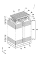
図1は、実施形態の半導体装置の模式平面図である。 FIG. 1 is a schematic plan view of the semiconductor device of the embodiment.
実施形態の半導体装置は、メモリセルアレイ1と、メモリセルアレイ1の外側の周辺領域に設けられた階段部2とを有する。メモリセルアレイ1および階段部2は同じ基板上に設けられている。
The semiconductor device according to the embodiment includes a
図2は、メモリセルアレイ1の模式斜視図である。
図3は、図1におけるA−A断面図である。
FIG. 2 is a schematic perspective view of the
3 is a cross-sectional view taken along the line AA in FIG.
図2において、基板10の主面に対して平行な方向であって相互に直交する2方向をX方向およびY方向とし、これらX方向およびY方向の双方に対して直交する方向をZ方向とする。他の図に示すX方向、Y方向、およびZ方向は、それぞれ、図2のX方向、Y方向、およびZ方向に対応する。
In FIG. 2, two directions parallel to the main surface of the
メモリセルアレイ1は、基板10と、積層体100と、基板10と積層体100との間に設けられたソース層SLと、複数の柱状部CLと、積層体100の上方に設けられた複数のビット線BLとを有する。
The
基板10は、例えばシリコン基板である。ソース層SLは、不純物がドープされた半導体層を有し、さらに金属を含む層を有することもできる。基板10とソース層SLとの間に絶縁層が設けられてもよい。
The
積層体100には複数の分離部60が設けられている。分離部60は、Z方向に沿って延び、ソース層SLに達する。さらに、分離部60はX方向に沿って延び、積層体100をY方向に複数のブロックに分離している。分離部60は、図3に示すように絶縁膜61から形成されている。
The stacked
柱状部CLは、積層体100内をZ方向に沿って延びる略円柱状に形成されている。複数の柱状部CLが例えば千鳥配置されている。または、複数の柱状部CLは、X方向およびY方向に沿って正方格子配置されていてもよい。
The columnar part CL is formed in a substantially cylindrical shape extending in the Z direction in the
複数のビット線BLは、Y方向に沿って延びる例えば金属膜である。複数のビット線BLは、X方向に互いに分離している。柱状部CLの後述する半導体ボディ20の上端部は、図2に示すコンタクトCbを介してビット線BLに接続されている。
The plurality of bit lines BL are, for example, metal films extending along the Y direction. The plurality of bit lines BL are separated from each other in the X direction. An upper end portion of a
積層体100は、基板10の主面に対して垂直な方向(Z方向)に積層された複数の電極層70を有する。複数の電極層70が、絶縁層(絶縁体)72を介してZ方向に積層されている。電極層70は、例えば金属層である。電極層70は、例えばタングステンまたはモリブデンを主成分に含む。
The
電極層70間の絶縁体は、空隙であってもよい。絶縁層72は、ソース層SLと、最下層の電極層70との間にも設けられている。
The insulator between the electrode layers 70 may be a gap. The insulating
絶縁膜42が最上層の電極層70上に設けられ、絶縁膜43が絶縁膜42上に設けられている。絶縁膜43は、柱状部CLの上端を覆っている。柱状部CLは、複数の電極層70および複数の絶縁層72を貫通して、ソース層SLに達する。
The insulating
図4は、実施形態のメモリセルMCの模式断面斜視図である。 FIG. 4 is a schematic cross-sectional perspective view of the memory cell MC of the embodiment.
柱状部CLは、メモリ膜30と、半導体ボディ20と、絶縁性のコア膜50とを有する。半導体ボディ20はパイプ状に形成され、その内側にコア膜50が設けられている。メモリ膜30は、電極層70と半導体ボディ20との間に設けられ、半導体ボディ20の周囲を囲んでいる。
The columnar portion CL includes a
半導体ボディ20は例えばシリコン膜であり、半導体ボディ20の下端部はソース層SLに接している。半導体ボディ20の上端部は、図2に示すコンタクトCbを介してビット線BLに接続している。
The
メモリ膜30は、トンネル絶縁膜31と、電荷蓄積膜(電荷蓄積部)32と、ブロック絶縁膜33とを含む積層膜である。電極層70と半導体ボディ20との間に、電極層70側から順に、ブロック絶縁膜33、電荷蓄積膜32、およびトンネル絶縁膜31が設けられている。
The
半導体ボディ20、メモリ膜30、および電極層70は、メモリセルMCを構成する。メモリセルMCは、半導体ボディ20の周囲を、メモリ膜30を介して、電極層70が囲んだ縦型トランジスタ構造を有する。
The
その縦型トランジスタ構造のメモリセルMCにおいて、半導体ボディ20はチャネルとして機能し、電極層70はコントロールゲートとして機能する。電荷蓄積膜32は半導体ボディ20から注入される電荷を蓄積するデータ記憶層として機能する。
In the memory cell MC having the vertical transistor structure, the
実施形態の半導体記憶装置は、データの消去・書き込みを電気的に自由に行うことができ、電源を切っても記憶内容を保持することができる不揮発性半導体記憶装置である。 The semiconductor memory device according to the embodiment is a nonvolatile semiconductor memory device that can electrically and freely erase and write data and can retain stored contents even when the power is turned off.
メモリセルMCは、例えばチャージトラップ型のメモリセルである。電荷蓄積膜32は、絶縁性の膜中に電荷を捕獲するトラップサイトを多数有するものであって、例えば、シリコン窒化膜を含む。または、電荷蓄積部は、まわりを絶縁体で囲まれた、導電性をもつ浮遊ゲートであってもよい。
The memory cell MC is, for example, a charge trap type memory cell. The
トンネル絶縁膜31は、半導体ボディ20から電荷蓄積膜32に電荷が注入される際、または電荷蓄積膜32に蓄積された電荷が半導体ボディ20に放出される際に電位障壁となる。トンネル絶縁膜31は、例えばシリコン酸化膜を含む。
The
ブロック絶縁膜33は、電荷蓄積膜32に蓄積された電荷が電極層70へ放出されるのを防止する。また、ブロック絶縁膜33は、電極層70から柱状部CLへの電荷のバックトンネリングを防止する。
The
ブロック絶縁膜33は、第1ブロック膜34と第2ブロック膜35を含む。第1ブロック膜34は例えばシリコン酸化膜であり、第2ブロック膜35は例えば金属酸化膜である。第1ブロック膜34は電荷蓄積膜32と第2ブロック膜35との間に設けられ、第2ブロック膜35は第1ブロック膜34と電極層70との間に設けられている。
The
図2に示すように、ドレイン側選択トランジスタSTDが積層体100の上層部に設けられ、ソース側選択トランジスタSTSが積層体100の下層部に設けられている。
As shown in FIG. 2, the drain side select transistor STD is provided in the upper layer portion of the
複数の電極層70のうち少なくとも最上層の電極層70はドレイン側選択トランジスタSTDのコントロールゲート(ドレイン側選択ゲート)として機能することが可能であり、少なくとも最下層の電極層70はソース側選択トランジスタSTSのコントロールゲート(ソース側選択ゲート)として機能することが可能である。
Among the plurality of electrode layers 70, at least the
複数のメモリセルMCが、ドレイン側選択トランジスタSTDとソース側選択トランジスタSTSとの間に設けられている。複数のメモリセルMC、ドレイン側選択トランジスタSTD、およびソース側選択トランジスタSTSは、柱状部CLの半導体ボディ20を通じて直列接続されている。複数のメモリセルMCがX方向、Y方向およびZ方向に3次元的に設けられている。
A plurality of memory cells MC are provided between the drain side select transistor STD and the source side select transistor STS. The plurality of memory cells MC, the drain side selection transistor STD, and the source side selection transistor STS are connected in series through the
積層体100および分離部60は、図1に示すように、メモリセルアレイ1が形成された領域から階段部2が形成された領域までX方向に沿って延びている。
As illustrated in FIG. 1, the
積層体100においてメモリセルアレイ1よりも外側に位置する部分に、階段部2が設けられている。その階段部2において、複数の電極層70は、X方向およびY方向のそれぞれの方向に沿って段差を形成して階段状に並んだ複数のテラス部70bをもつ。
A
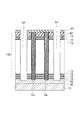
図5は、階段部2の模式断面図である。
FIG. 5 is a schematic cross-sectional view of the
図5には、複数の電極層70のうち、メモリセルMCのコントロールゲートとして機能する任意の6層の電極層WL1、WL2、WL3、WL4、WL5、WL6が積層された部分における電極層WL1のテラス部WL1bと電極層WL2のテラス部WL2bとがX方向に沿って形成する段差部の断面を表す。図5における右方向への延長領域にメモリセルアレイ1が設けられている。
FIG. 5 illustrates the electrode layer WL1 in a portion where any six electrode layers WL1, WL2, WL3, WL4, WL5, and WL6 that function as the control gate of the memory cell MC among the plurality of electrode layers 70 are stacked. The cross section of the level | step-difference part which the terrace part WL1b and the terrace part WL2b of electrode layer WL2 form along a X direction is represented. The
1ステップを形成するテラス部WL1b、WL2bをそれぞれもつ電極層WL1と電極層WL2との間には、1層以上の他の電極層WL3、WL4が設けられている。テラス部WL2bより下段の他のテラス部(図示せず)をもつ電極層(図示せず)と、電極層WL2との間には、1層以上の他の電極層WL5、WL6が設けられている。 One or more other electrode layers WL3 and WL4 are provided between the electrode layer WL1 and the electrode layer WL2 each having the terrace portions WL1b and WL2b forming one step. One or more other electrode layers WL5 and WL6 are provided between an electrode layer (not shown) having another terrace portion (not shown) below the terrace portion WL2b and the electrode layer WL2. Yes.
電極層WL1の下に電極層WL3が設けられ、電極層WL3の下に電極層WL4が設けられ、電極層WL4の下に電極層WL2が設けられ、電極層WL2の下に電極層WL5が設けられ、電極層WL5の下に電極層WL6が設けられている。それら電極層WL1〜WL6のそれぞれの間に絶縁層72が設けられている。
An electrode layer WL3 is provided below the electrode layer WL1, an electrode layer WL4 is provided below the electrode layer WL3, an electrode layer WL2 is provided below the electrode layer WL4, and an electrode layer WL5 is provided below the electrode layer WL2. The electrode layer WL6 is provided under the electrode layer WL5. An insulating
電極層WL1は、メモリセルアレイ1が形成された領域へと続く薄化部WL1aと、薄化部WL1aよりも厚いテラス部WL1bとを有する。
The electrode layer WL1 includes a thinned portion WL1a that continues to the region where the
電極層WL2は、メモリセルアレイ1が形成された領域へと続く薄化部WL2aと、薄化部WL2aよりも厚いテラス部WL2bとを有する。電極層WL2のテラス部WL2bは、電極層WL1のテラス部WL1bとの間に階段状の段差をもってテラス部WL1bの下段側に設けられ、テラス部WL1bのエッジWL1cよりもX方向に沿って突出している。
The electrode layer WL2 includes a thinned portion WL2a that continues to the region where the
電極層WL3は、1層の絶縁層72を挟んで、電極層WL1の下に設けられている。電極層WL3は、電極層WL2の薄化部WL2aと、電極層WL1との間に設けられている。電極層WL3は、電極層WL1のテラス部WL1bのエッジWL1cよりも、電極層WL2のテラス部WL2bの突出方向(図5において左方向)の反対方向(図5において右方向)に後退したエッジWL3cを有する。
The electrode layer WL3 is provided under the electrode layer WL1 with the one insulating
電極層WL4は、1層の絶縁層72を挟んで、電極層WL3の下に設けられている。電極層WL4は、電極層WL2の薄化部WL2aと、電極層WL3との間に設けられている。電極層WL4は、電極層WL1のテラス部WL1bのエッジWL1cおよび電極層WL3のエッジWL3cよりも、電極層WL2のテラス部WL2bの突出方向の反対方向に後退したエッジWL4cを有する。
The electrode layer WL4 is provided below the electrode layer WL3 with one insulating
電極層WL5は、1層の絶縁層72を挟んで、電極層WL2の下に設けられている。電極層WL5は、電極層WL2のテラス部WL2bのエッジWL2cよりも、テラス部WL2bの突出方向の反対方向に後退したエッジWL5cを有する。
The electrode layer WL5 is provided below the electrode layer WL2 with one insulating
電極層WL6は、1層の絶縁層72を挟んで、電極層WL5の下に設けられている。電極層WL6は、電極層WL2のテラス部WL2bのエッジWL2cおよび電極層WL5のエッジWL5cよりも、テラス部WL2bの突出方向の反対方向に後退したエッジWL6cを有する。
The electrode layer WL6 is provided below the electrode layer WL5 with one insulating
以下の説明において、「後退」とは、図5において右方向への後退を表す。 In the following description, “retreat” represents a retreat in the right direction in FIG.
テラス部WL1bの下に位置する電極層WL3、WL4のエッジWL3c、WL4cは、上のテラス部WL1bのエッジWL1cよりも、メモリセルアレイ1が形成された領域に向かって後退している。より下層の電極層WL4のエッジWL4cほど、上層の電極層WL3のエッジWL3cよりも後退している。
The edges WL3c and WL4c of the electrode layers WL3 and WL4 located below the terrace portion WL1b are set back from the edge WL1c of the upper terrace portion WL1b toward the region where the
テラス部WL2bの下に位置する電極層WL5、WL6のエッジWL5c、WL6cは、上のテラス部WL2bのエッジWL2cよりも、メモリセルアレイ1が形成された領域に向かって後退している。より下層の電極層WL6のエッジWL6cほど、上層の電極層WL5のエッジWL5cよりも後退している。
The edges WL5c and WL6c of the electrode layers WL5 and WL6 located under the terrace portion WL2b are set back from the edge WL2c of the upper terrace portion WL2b toward the region where the
テラス部WL1bの下の複数の絶縁層72のそれぞれのエッジ72cも、テラス部WL1bのエッジWL1cよりも後退している。
Each
電極層WL3と電極層WL4との間の絶縁層72のエッジ72cは、電極層WL1と電極層WL3との間の絶縁層72のエッジ72c、および電極層WL3のエッジWL3cよりも後退している。電極層WL4と電極層WL2との間の絶縁層72のエッジ72cは、電極層WL3と電極層WL4との間の絶縁層72のエッジ72c、および電極層WL4のエッジWL4cよりも後退している。
The
電極層WL3のエッジWL3cは、X方向およびZ方向に対して傾斜した傾斜面であり、その傾斜面と電極層WL3の下面との間の角部は、傾斜面と電極層WL3の上面との間の角部よりも後退している。 The edge WL3c of the electrode layer WL3 is an inclined surface inclined with respect to the X direction and the Z direction, and a corner between the inclined surface and the lower surface of the electrode layer WL3 is formed between the inclined surface and the upper surface of the electrode layer WL3. It is retreating from the corner between.
電極層WL4のエッジWL4cは、X方向およびZ方向に対して傾斜した傾斜面であり、その傾斜面と電極層WL4の下面との間の角部は、傾斜面と電極層WL4の上面との間の角部よりも後退している。 The edge WL4c of the electrode layer WL4 is an inclined surface inclined with respect to the X direction and the Z direction, and a corner between the inclined surface and the lower surface of the electrode layer WL4 is formed between the inclined surface and the upper surface of the electrode layer WL4. It is retreating from the corner between.
電極層WL1と電極層WL2との間の3層の絶縁層72のそれぞれのエッジ72cも傾斜面である。これら3層の絶縁層72のエッジ72c、電極層WL3のエッジWL3c、および電極層WL4のエッジWL4cは、テラス部WL1bのエッジWL1cから電極層WL2の上面にかけて、傾斜面を形成して連続している。また、電極層WL1のテラス部WL1bのエッジWL1cにも、これより下の層が形成する上記傾斜面に続く傾斜面が設けられている。電極層WL1のテラス部WL1bは、電極層WL2のテラス部WL2bに面する角部が面取りされて上記傾斜面が形成された形状とされている。
Each
テラス部WL2bの下の複数の絶縁層72のそれぞれのエッジ72cも、テラス部WL2bのエッジWL2cよりも後退している。
Each
テラス部WL2bの下の層のエッジにも、テラス部WL1bの下の層のエッジと同様に、テラス部WL2bのエッジWL2cの一部から続く傾斜面が形成されている。 Similarly to the edge of the layer under the terrace portion WL1b, an inclined surface that continues from a part of the edge WL2c of the terrace portion WL2b is formed at the edge of the layer under the terrace portion WL2b.
階段部2の表面は絶縁膜45で覆われている。絶縁膜45は、テラス部WL1bの上面、およびテラス部WL2bの上面を覆っている。
The surface of the
絶縁膜45は、電極層WL1のテラス部WL1bのエッジWL1c、電極層WL3のエッジWL3c、電極層WL4のエッジWL4c、電極層WL2のテラス部WL2bのエッジWL2c、電極層WL5のエッジWL5c、電極層WL6のエッジWL6c、および絶縁層72のエッジ72cを覆っている。
The insulating
絶縁膜45は、電極層WL1のテラス部WL1bの下の層のエッジが形成する上記傾斜面と、電極層WL2との間を埋めている。
The insulating
絶縁膜45上に、階段部2の段差を埋めるように、絶縁膜46が設けられている。絶縁膜45および絶縁膜46は、例えばシリコン酸化膜である。
An insulating
テラス部WL1b、WL2b上にコンタクト部CCが設けられている。コンタクト部CCは、略円柱状の導電体である。コンタクト部CCは、絶縁膜46内をZ方向に沿って延び、絶縁膜45を貫通して、テラス部WL1b、WL2bに接続している。
A contact portion CC is provided on the terrace portions WL1b and WL2b. The contact part CC is a substantially cylindrical conductor. The contact portion CC extends in the Z direction in the insulating
コンタクト部CCは、図示しない上層配線と接続されている。その上層配線は、例えば基板10の表面に形成された制御回路と電気的に接続されている。
The contact part CC is connected to an upper layer wiring (not shown). The upper layer wiring is electrically connected to a control circuit formed on the surface of the
絶縁膜46を形成した後、その絶縁膜46内をZ方向に沿って延び、各テラス部WL1b、WL2b(70b)に達する複数のコンタクトホールが形成される。そのコンタクトホール内に導電材が形成され、コンタクト部CCが形成される。
After the insulating
複数のコンタクトホールは、例えばRIE(Reactive Ion Etching)で一括形成される。より下段側のテラス部70bに達する深いコンタクトホールと、より上段側のテラス部70bに達する浅いコンタクトホールが同時に形成される。このようなエッチング深さの差によって、例えば浅いコンタクトホールが、接続対象のテラス部70bを貫通して、そのテラス部70bの下の他の電極層70に到達することが懸念され得る。これは、コンタクト部CCを通じた異なる電極層70どうしのショートをまねく。
The plurality of contact holes are collectively formed by, for example, RIE (Reactive Ion Etching). A deep contact hole reaching the
そこで、実施形態によれば、テラス部70bを厚膜化することで、コンタクトホールを形成するエッチングをテラス部70bで確実にストップし、テラス部70bの下にコンタクトホールが突き抜けないようにできる。
Therefore, according to the embodiment, by increasing the thickness of the
後述するように、電極層70のテラス部70bとなる部分の上面に膜を積み増すことで、厚いテラス部70bが得られる。したがって、テラス部70bは、上方に突出するように厚膜化される。テラス部70bが上方に向かって厚くなると、階段部2の側壁付近に位置する他の電極層70のエッジと、テラス部70bとの間の距離が近くなり、それら両者間の耐圧の低下が懸念される。
As will be described later, a
そこで、図5に示す例では、電極層WL3のエッジWL3cおよび電極層WL4のエッジWL4cを階段部2の側壁から遠ざけるように後退させることで、それらエッジWL3c、WL4cと、厚膜化したテラス部WL2bとの間の距離を広げることができる。これは、電極層WL2のテラス部WL2bと電極層WL3との間の耐圧、および電極層WL2のテラス部WL2bと電極層WL4との間の耐圧を向上させる。
Therefore, in the example shown in FIG. 5, by retreating the edge WL3c of the electrode layer WL3 and the edge WL4c of the electrode layer WL4 away from the side wall of the
特に、よりテラス部WL2bに近い電極層WL4のエッジWL4cを、電極層WL3のエッジWL3cよりも後退させることで、電極層WL2のテラス部WL2bと、電極層WL4との間の耐圧を確実に向上させることができる。 In particular, by retreating the edge WL4c of the electrode layer WL4 closer to the terrace portion WL2b than the edge WL3c of the electrode layer WL3, the breakdown voltage between the terrace portion WL2b of the electrode layer WL2 and the electrode layer WL4 is reliably improved. Can be made.
また、電極層WL3、WL4のエッジWL3c、WL4cは傾斜面であり、その傾斜面における、よりテラス部WL2bに近い下方の角部の方が、上方の角部よりも後退している。このようなエッジ形状は、テラス部WL2bと、電極層WL3、WL4との間の耐圧向上に有利である。 Further, the edges WL3c and WL4c of the electrode layers WL3 and WL4 are inclined surfaces, and the lower corner portion closer to the terrace portion WL2b on the inclined surface recedes from the upper corner portion. Such an edge shape is advantageous for improving the breakdown voltage between the terrace portion WL2b and the electrode layers WL3 and WL4.
次に、実施形態の半導体装置の製造方法について説明する。
まず、図6〜図14を参照して、メモリセルアレイ1の製造方法について説明する。
Next, a method for manufacturing the semiconductor device of the embodiment will be described.
First, a manufacturing method of the
図6に示すように、ソース層SLが基板10上に形成され、複数の犠牲層71と複数の絶縁層72とを含む積層体100がソース層SL上に形成される。例えば、犠牲層71はシリコン窒化層であり、絶縁層72はシリコン酸化層である。
As shown in FIG. 6, the source layer SL is formed on the
ソース層SLの表面に絶縁層72が形成され、その絶縁層72の上に犠牲層71が形成される。以降、絶縁層72と犠牲層71とを交互に積層する工程が繰り返される。最上層の犠牲層71上に絶縁膜42が形成される。
An insulating
図7に示すように、複数のメモリホールMHが積層体100に形成される。メモリホールMHは、図示しないマスクを用いたRIEで形成される。メモリホールMHは、積層体100を貫通し、ソース層SLに達する。
As shown in FIG. 7, a plurality of memory holes MH are formed in the
図8に示すように、メモリホールMHの側面および底面にコンフォーマルに積層膜30aが形成される。積層膜30aは、図4に示すトンネル絶縁膜31と電荷蓄積膜32とを含む。その積層膜30aの内側には、図9に示すようにカバー半導体膜20aがコンフォーマルに形成される。
As shown in FIG. 8, a
その後、図10に示すように、積層体100上にマスク層95が形成され、RIEによって、メモリホールMHの底面に形成されたカバー半導体膜20aおよび積層膜30aが除去される。このRIEのとき、メモリホールMHの側面に形成された積層膜30aは、カバー半導体膜20aで覆われて保護されている。メモリホールMHの側面に形成された積層膜30aはRIEのダメージを受けない。
Thereafter, as shown in FIG. 10, a
マスク層95を除去した後、図11に示すように、メモリホールMH内に半導体膜20bが形成される。半導体膜20bは、カバー半導体膜20aの側面、およびソース層SLが露出するメモリホールMHの底面に形成される。
After removing the
カバー半導体膜20aおよび半導体膜20bは、例えばアモルファスシリコン膜として形成された後、熱処理により多結晶シリコン膜に結晶化される。カバー半導体膜20aおよび半導体膜20bは前述した半導体ボディ20を構成する。
The
半導体膜20bの内側には、図12に示すように、コア膜50が形成される。このようにして、積層膜30a、半導体ボディ20、およびコア膜50を含む柱状部CLが形成される。
As shown in FIG. 12, a
図12に示す絶縁膜42上に堆積した膜は、CMP(chemical mechanical polishing)またはエッチバックにより除去される。
The film deposited on the insulating
その後、図13に示すように、絶縁膜42上に絶縁膜43が形成される。絶縁膜43は、柱状部CLの上端を覆う。そして、図示しないマスクを用いたRIEにより、絶縁膜43、絶縁膜42、複数の犠牲層71、および複数の絶縁層72を含む積層体100に、複数のスリットSTを形成する。スリットSTは、積層体100を貫通し、ソース層SLに達する。
Thereafter, as shown in FIG. 13, an insulating
次に、スリットSTを通じて供給されるエッチングガスまたはエッチング液により、犠牲層71を除去する。例えば、燐酸を含む溶液によって、シリコン窒化層である犠牲層71が除去される。犠牲層71が除去され、図14に示すように、積層方向で隣り合う絶縁層72の間に空隙73が形成される。空隙73は、絶縁膜42と、最上層の絶縁層72との間にも形成される。
Next, the
複数の絶縁層72は、複数の柱状部CLの側面を囲むように、その側面に接している。複数の絶縁層72は、このような複数の柱状部CLとの物理的結合によって支えられ、空隙73が保たれる。
The plurality of insulating
空隙73の内壁には、図4に示す、第1ブロック膜34、第2ブロック膜35、およびバリアメタル81が順に形成される。第1ブロック膜34、第2ブロック膜35、およびバリアメタル81は、絶縁層72の上面、下面、および柱状部CLの側面に沿ってコンフォーマルに形成される。バリアメタル81として例えば窒化チタン膜が形成される。
On the inner wall of the
バリアメタル81を形成した後、空隙73はまだ残っている。その残った空隙73内に電極層70が埋め込まれる。例えば、フッ化タングステンと水素とを含むガスを用いたCVD(Chemical Vapor Deposition)或いはALD(Atomic Layer Deposition)で、電極層70としてタングステン層が形成される。
After the
その後、スリットST内に、図3に示す絶縁膜61が形成され、分離部60が形成される。
Thereafter, the insulating
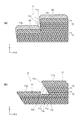
次に、図15(a)〜図24を参照して、図5に示す階段部2の製造方法について説明する。
Next, a method for manufacturing the
図15(a)は、複数の犠牲層71と複数の絶縁層72とを含む積層体100の一部の斜視図である。
FIG. 15A is a perspective view of a part of the
図15(a)において斜線で示す領域をレジストで覆った状態で、そのレジストから露出している領域の絶縁層72および犠牲層71をそれぞれ1層ずつRIEでエッチングする。このエッチング後の状態を図15(b)に表す。
In the state where the hatched region in FIG. 15A is covered with a resist, the insulating
さらに、図15(b)において斜線で示す領域をレジストで覆った状態で、そのレジストから露出している領域の絶縁層72および犠牲層71をそれぞれ1層ずつRIEでエッチングする。
Further, in the state where the hatched region in FIG. 15B is covered with the resist, the insulating
このようにして、図16(a)に示すように、積層体100の一部に、Y方向に沿った階段列が形成される。ある犠牲層71と、その1層下または1層上の犠牲層71とが、Y方向に沿った階段列の1ステップを構成する。
In this way, as shown in FIG. 16A, a staircase array along the Y direction is formed in a part of the
次に、図16(a)において斜線で示す領域をレジストで覆った状態で、そのレジストから露出している領域の絶縁層72および犠牲層71をそれぞれ複数層(例えば3層)ずつRIEでエッチングする。このエッチング後の状態を図16(b)に表す。
Next, in a state where the hatched region in FIG. 16A is covered with a resist, the insulating
さらに、図16(b)において斜線で示す領域をレジストで覆った状態で、そのレジストから露出している領域の絶縁層72および犠牲層71をそれぞれ3層ずつRIEでエッチングする。このエッチング後の状態を図17(a)に表す。
Further, in the state where the hatched region in FIG. 16B is covered with the resist, the insulating
さらに、図17(a)において斜線で示す領域をレジストで覆った状態で、そのレジストから露出している領域の絶縁層72および犠牲層71をそれぞれ3層ずつRIEでエッチングする。
Further, in a state where the hatched region in FIG. 17A is covered with a resist, the insulating
このようにして、図17(b)に示すように、積層体100の一部に、X方向に沿った階段列が形成される。ある犠牲層71と、その3層下または3層上の犠牲層71とが、X方向に沿った階段列の1ステップを構成する。
In this way, as shown in FIG. 17B, a staircase array along the X direction is formed in a part of the
先の工程で形成されたY方向に沿った階段列に加えて、X方向にも階段列を有する階段部2’が形成される。その階段部2’における最表層を構成する絶縁層72をRIEで除去する。
In addition to the staircase row along the Y direction formed in the previous step, a
これにより、図18に示すように、複数の犠牲層71の複数のテラス部71bが最表層に露出してX方向およびY方向に階段状に並んだ階段部2’が得られる。
As a result, as shown in FIG. 18, a plurality of
図19(a)は、階段部2’におけるX方向に沿った任意の1ステップを構成する部分の断面図である。
FIG. 19A is a cross-sectional view of a portion constituting an arbitrary step along the X direction in the
犠牲層71のテラス部71bの上に、犠牲層71と同じ材料の膜(例えばシリコン窒化膜)71’を、例えばCVD法で形成し、図19(b)に示すようにテラス部71bを厚膜化する。
On the
その後、図20(a)に示すように、カバレッジ(段差被覆性)の悪い保護膜91をテラス部71b上に形成する。例えば、保護膜91としてカーボン膜をCVD法で形成する。そして、保護膜91をマスクにして、例えばCF4等のフッ化炭素を含むガスを用いたエッチングにより、階段部2’の側壁に形成された膜71’を除去する。
Thereafter, as shown in FIG. 20A, a
上段のテラス部71bと下段のテラス部71bとをつなぐように階段部2’の側壁を覆っていた膜71’が除去される。この後、保護膜91を除去して、図20(b)に示すように、犠牲層71においてテラス部71bのみが厚膜化される。
The
その厚膜化されたテラス部71b上に、図21(a)に示すように、再びカバレッジの悪い保護膜92を形成する。例えば、保護膜92としてカーボン膜をCVD法で形成する。
As shown in FIG. 21A, a
階段部2’の側壁は、テラス部71bのエッジ71c、そのエッジ71cの下方に続いている犠牲層71のエッジ71cおよび絶縁層72のエッジ72cによって形成される。その階段部2’の側壁には、テラス部71b上の保護膜92の膜厚よりも薄い膜厚の保護膜92が形成される。階段部2’の側壁に形成された保護膜92の膜厚は、上段のテラス部71bに近い上部ほど厚くなり、下段のテラス部71bに近い下部ほど薄くなる。この状態で、犠牲層71に対するエッチングを行う。
The side wall of the
例えばCF4等のフッ化炭素を含むガスを用いて、シリコン窒化層である犠牲層71をエッチングする。このとき、シリコン酸化層である絶縁層72も、犠牲層71とほぼ同レートでエッチングされる。
For example, the
または、図25に示すように、犠牲層71のみを選択的に後退させることもできる。
Alternatively, as shown in FIG. 25, only the
保護膜92が薄い階段部2’の側壁から犠牲層71および絶縁層72に対してエッチングが進行し、階段部2’の側壁に位置していた犠牲層71のエッジ71cおよび絶縁層72のエッジ72cが、図21(b)に示すように階段部2’の側壁からX方向に沿って後退する。
Etching proceeds to the
階段部2’の側壁において保護膜92の膜厚がより薄い下部ほど犠牲層71および絶縁層72の後退量が大きくなり、図21(b)に示すように、階段部2’の側壁に傾斜面が形成される。上段のテラス部71bのエッジ71cの一部から、下方に向かうにしたがって下段のテラス部71bから遠ざかるように傾斜面が形成される。
The lower the thickness of the
この後、図22(a)に示すように、階段部2’の表面を覆うように絶縁膜45を形成する。例えば、絶縁膜45としてシリコン酸化膜をALD法で形成する。絶縁膜45は、テラス部71bの上面を覆う。
Thereafter, as shown in FIG. 22A, an insulating
また、絶縁膜45は、犠牲層71のエッジ71cおよび絶縁層72のエッジ72cの後退により形成された傾斜面の下方の空隙を埋め、犠牲層71のエッジ71cおよび絶縁層72のエッジ72cを覆う。
Further, the insulating
犠牲層71だけでなく絶縁層72も後退させることで、図25の場合に比べて、階段部2’の側壁の凹凸を少なくできる。そのため、犠牲層71のエッジ71cが面する空隙への絶縁膜45の埋め込み性に優れ、犠牲層71のエッジ71cを絶縁膜45で確実に覆うことができる。
By retreating not only the
絶縁膜45を形成した後、図22(b)に示すように、絶縁膜45上に絶縁膜46を形成する。絶縁膜46は、階段部2’の段差を埋める。例えば、絶縁膜46としてCVD法でシリコン酸化膜を形成する。
After forming the insulating
絶縁膜46を形成した後、前述したメモリセルアレイ1が形成される領域に柱状部CLが形成される。さらに、スリットSTが形成され、そのスリットSTを通じたエッチングにより犠牲層71を除去する。階段部2’においても犠牲層71が除去され、図23(a)に示すように、絶縁層72間に空隙73が形成される。さらに、絶縁膜46および絶縁膜45で覆われたテラス部となる部分にも空隙73が形成される。
After forming the insulating
そして、スリットSTを通じて空隙73に電極層70の材料が埋め込まれ、図23(b)に示す階段部2が形成される。絶縁膜45は、犠牲層71のエッジ71cを覆う位置まで確実に形成されていたため、図23(a)に示す工程で形成される空隙73のエッジ73cの位置を、後退させた犠牲層71のエッジ71cの位置に一致させることができる。この結果、図23(b)に示すように、空隙73に形成された電極層WL3のエッジWL3cおよび電極層WL4のエッジWL4cを、テラス部WL2bから後退した位置に位置させることができる。
And the material of the
その後、図24に示すように、絶縁膜46および絶縁膜45を貫通して各テラス部WL1b、WL2bに達するコンタクトホールCHが形成される。
Thereafter, as shown in FIG. 24, contact holes CH that penetrate through the insulating
複数のコンタクトホールCHがRIEで一括形成される。テラス部WL1b、WL2bは厚膜化されているため、各コンタクトホールCHをテラス部WL1b、WL2bで確実にストップさせることができる。 A plurality of contact holes CH are collectively formed by RIE. Since the terrace portions WL1b and WL2b are thickened, the contact holes CH can be reliably stopped at the terrace portions WL1b and WL2b.
その後、コンタクトホールCH内に導電材料が形成され、図5に示すコンタクト部CCが形成される。 Thereafter, a conductive material is formed in the contact hole CH, and the contact portion CC shown in FIG. 5 is formed.
実施形態によれば、厚膜化したテラス部WL2bの近くにある電極層WL3、WL4のエッジWL3c、WL4cをテラス部WL2bから遠ざけるように後退させているため、テラス部WL2bと、他の電極層WL3、WL4との耐圧を高めることができる。 According to the embodiment, since the edges WL3c and WL4c of the electrode layers WL3 and WL4 in the vicinity of the thickened terrace portion WL2b are retracted away from the terrace portion WL2b, the terrace portion WL2b and the other electrode layers The breakdown voltage with WL3 and WL4 can be increased.
厚膜化したテラス部WL2bのX方向の幅を縮小することで、テラス部WL2bと、電極層WL3、WL4のエッジWL3c、WL4cとの距離を大きくするのではない。そのため、コンタクト部CCがテラス部WL2bを外れてしまわないようにテラス幅のマージンは確保できる。 The distance between the terrace portion WL2b and the edges WL3c and WL4c of the electrode layers WL3 and WL4 is not increased by reducing the width in the X direction of the thickened terrace portion WL2b. Therefore, a margin of the terrace width can be secured so that the contact part CC does not deviate from the terrace part WL2b.
以上説明した複数の電極層70の階段部2の構造は、メモリセルMCのコントロールゲートに限らず、ドレイン側選択トランジスタSTDの選択ゲート、ソース側選択トランジスタSTSの選択ゲートにも適用できる。
The structure of the stepped
本発明のいくつかの実施形態を説明したが、これらの実施形態は、例として提示したものであり、発明の範囲を限定することは意図していない。これら新規な実施形態は、その他の様々な形態で実施されることが可能であり、発明の要旨を逸脱しない範囲で、種々の省略、置き換え、変更を行うことができる。これら実施形態やその変形は、発明の範囲や要旨に含まれるとともに、特許請求の範囲に記載された発明とその均等の範囲に含まれる。 Although several embodiments of the present invention have been described, these embodiments are presented by way of example and are not intended to limit the scope of the invention. These novel embodiments can be implemented in various other forms, and various omissions, replacements, and changes can be made without departing from the scope of the invention. These embodiments and modifications thereof are included in the scope and gist of the invention, and are included in the invention described in the claims and the equivalents thereof.
2…階段部、45,46…絶縁膜、70,WL1〜WL6…電極層、70b,WL1b,WL2b…テラス部、WL1c,WL2c,WL3c,WL4c,WL5c,WL6c…エッジ、71…犠牲層、72…絶縁層 2 ... Staircase, 45, 46 ... Insulating film, 70, WL1 to WL6 ... Electrode layer, 70b, WL1b, WL2b ... Terrace, WL1c, WL2c, WL3c, WL4c, WL5c, WL6c ... Edge, 71 ... Sacrificial layer, 72 ... insulation layer
Claims (5)
前記複数の電極層は、
第1部分と、前記第1部分よりも厚い第2部分とを有する第1電極層と、
第3部分と、前記第3部分よりも厚い第4部分とを有する第2電極層であって、前記第4部分は、前記第1電極層の前記第2部分との間に階段状の段差をもって前記第2部分の下段側に設けられ、前記第2部分のエッジよりも第1方向に沿って突出している、第2電極層と、
前記第2電極層の前記第3部分と、前記第1電極層との間に設けられた第3電極層と、
を有し、
前記第3電極層は、前記第1電極層の前記第2部分の前記エッジよりも、前記第2電極層の前記第4部分の突出方向の反対方向に後退したエッジを有する半導体装置。 Comprising a laminate having a plurality of electrode layers laminated via an insulator;
The plurality of electrode layers are:
A first electrode layer having a first portion and a second portion thicker than the first portion;
A second electrode layer having a third part and a fourth part thicker than the third part, wherein the fourth part is a stepped step between the second part of the first electrode layer A second electrode layer provided on the lower side of the second part and projecting along the first direction from the edge of the second part;
A third electrode layer provided between the third portion of the second electrode layer and the first electrode layer;
Have
The semiconductor device, wherein the third electrode layer has an edge that recedes in a direction opposite to a protruding direction of the fourth portion of the second electrode layer from the edge of the second portion of the first electrode layer.
前記第3電極層の下面と前記傾斜面との間の角部は、前記第3電極層の上面と前記傾斜面との間の角部よりも、前記反対方向に後退している請求項1記載の半導体装置。 The edge of the third electrode layer is an inclined surface;
2. The corner between the lower surface of the third electrode layer and the inclined surface recedes in the opposite direction from the corner between the upper surface of the third electrode layer and the inclined surface. The semiconductor device described.
前記第4電極層は、前記第3電極層の前記エッジよりも、前記反対方向に後退したエッジを有する請求項1または2に記載の半導体装置。 A fourth electrode layer provided between the third electrode layer and the third portion of the second electrode layer;
3. The semiconductor device according to claim 1, wherein the fourth electrode layer has an edge that recedes in the opposite direction from the edge of the third electrode layer.
前記第1絶縁層のエッジは、前記第1電極層の前記第2部分の前記エッジよりも、前記反対方向に後退している請求項1〜3のいずれか1つに記載の半導体装置。 The insulator has a first insulating layer provided between the second portion of the first electrode layer and the third electrode layer;
4. The semiconductor device according to claim 1, wherein an edge of the first insulating layer recedes in the opposite direction with respect to the edge of the second portion of the first electrode layer.
前記半導体ボディと前記電極層との間に設けられた電荷蓄積部と、
をさらに備えた請求項1〜4のいずれか1つに記載の半導体装置。 A semiconductor body extending in the stacking direction of the stacked body in the stacked body;
A charge storage portion provided between the semiconductor body and the electrode layer;
The semiconductor device according to claim 1, further comprising:
Priority Applications (2)
| Application Number | Priority Date | Filing Date | Title |
|---|---|---|---|
| JP2018092888A JP2019201028A (en) | 2018-05-14 | 2018-05-14 | Semiconductor device |
| US16/123,148 US10916557B2 (en) | 2018-05-14 | 2018-09-06 | Semiconductor device |
Applications Claiming Priority (1)
| Application Number | Priority Date | Filing Date | Title |
|---|---|---|---|
| JP2018092888A JP2019201028A (en) | 2018-05-14 | 2018-05-14 | Semiconductor device |
Publications (1)
| Publication Number | Publication Date |
|---|---|
| JP2019201028A true JP2019201028A (en) | 2019-11-21 |
Family
ID=68464211
Family Applications (1)
| Application Number | Title | Priority Date | Filing Date |
|---|---|---|---|
| JP2018092888A Pending JP2019201028A (en) | 2018-05-14 | 2018-05-14 | Semiconductor device |
Country Status (2)
| Country | Link |
|---|---|
| US (1) | US10916557B2 (en) |
| JP (1) | JP2019201028A (en) |
Families Citing this family (2)
| Publication number | Priority date | Publication date | Assignee | Title |
|---|---|---|---|---|
| WO2019218351A1 (en) * | 2018-05-18 | 2019-11-21 | Yangtze Memory Technologies Co., Ltd. | Staircase formation in three-dimensional memory device |
| JP2021145063A (en) * | 2020-03-12 | 2021-09-24 | キオクシア株式会社 | Semiconductor storage device |
Family Cites Families (17)
| Publication number | Priority date | Publication date | Assignee | Title |
|---|---|---|---|---|
| KR101065140B1 (en) * | 2008-03-17 | 2011-09-16 | 가부시끼가이샤 도시바 | Semiconductor storage device |
| JP2014027104A (en) | 2012-07-26 | 2014-02-06 | Toshiba Corp | Semiconductor device and manufacturing method of the same |
| KR102003529B1 (en) | 2012-08-22 | 2019-07-25 | 삼성전자주식회사 | Methods of forming a stack of electrodes and three-dimensional semiconductor devices fabricated thereby |
| KR102024723B1 (en) * | 2013-01-02 | 2019-09-24 | 삼성전자주식회사 | Three dimensional semiconductor device |
| KR20150073251A (en) | 2013-12-20 | 2015-07-01 | 에스케이하이닉스 주식회사 | Semiconductor device and method of manufacturing the same |
| KR20150104817A (en) | 2014-03-06 | 2015-09-16 | 에스케이하이닉스 주식회사 | Semiconductor device and method of manufacturing the same |
| JP6203152B2 (en) * | 2014-09-12 | 2017-09-27 | 東芝メモリ株式会社 | Manufacturing method of semiconductor memory device |
| US9698157B2 (en) * | 2015-03-12 | 2017-07-04 | Kabushiki Kaisha Toshiba | Microstructure device and method for manufacturing the same |
| US9679906B2 (en) | 2015-08-11 | 2017-06-13 | Sandisk Technologies Llc | Three-dimensional memory devices containing memory block bridges |
| KR102422087B1 (en) | 2015-09-23 | 2022-07-18 | 삼성전자주식회사 | Vertical memory devices and methods of manufacturing the same |
| WO2017087820A1 (en) * | 2015-11-19 | 2017-05-26 | Fu-Chang Hsu | Methods and apparatus for a 3d array inside a substrate trench |
| KR102497116B1 (en) * | 2015-12-30 | 2023-02-07 | 에스케이하이닉스 주식회사 | Electronic device and method for fabricating the same |
| US10134672B2 (en) | 2016-03-15 | 2018-11-20 | Toshiba Memory Corporation | Semiconductor memory device having a stepped structure and contact wirings formed thereon |
| KR102619876B1 (en) * | 2016-07-19 | 2024-01-03 | 삼성전자주식회사 | Memory device |
| KR102630925B1 (en) * | 2016-09-09 | 2024-01-30 | 삼성전자주식회사 | Semiconductor device including stack structure |
| JP2018148071A (en) * | 2017-03-07 | 2018-09-20 | 東芝メモリ株式会社 | Storage device |
| JP2018152419A (en) * | 2017-03-10 | 2018-09-27 | 東芝メモリ株式会社 | Semiconductor memory device |
-
2018
- 2018-05-14 JP JP2018092888A patent/JP2019201028A/en active Pending
- 2018-09-06 US US16/123,148 patent/US10916557B2/en active Active
Also Published As
| Publication number | Publication date |
|---|---|
| US20190348431A1 (en) | 2019-11-14 |
| US10916557B2 (en) | 2021-02-09 |
Similar Documents
| Publication | Publication Date | Title |
|---|---|---|
| JP6842386B2 (en) | Semiconductor device | |
| TWI645458B (en) | Semiconductor device and its manufacturing method | |
| TWI635598B (en) | Semiconductor device and its manufacturing method | |
| JP6434877B2 (en) | Semiconductor device | |
| CN107833888B (en) | Semiconductor device and method for manufacturing the same | |
| CN108735748B (en) | Three-dimensional semiconductor device | |
| CN110277395B (en) | Storage device | |
| US20210375886A1 (en) | Method of manufacturing a three-dimensional non-volatile memory device | |
| JP2013258360A (en) | Semiconductor device manufacturing method and semiconductor device | |
| JP2019009383A (en) | Semiconductor device and manufacturing method of the same | |
| CN109003982B (en) | 3D memory device and method of manufacturing the same | |
| JP2018163963A (en) | Semiconductor device and manufacturing method thereof | |
| CN109119424B (en) | 3D memory device and method of manufacturing the same | |
| JP2009004517A (en) | Nonvolatile semiconductor memory device and method for manufacturing the same | |
| CN109390348A (en) | 3D memory device and its manufacturing method | |
| KR20140018541A (en) | Nonvolatile memory device and method for fabricating the same | |
| JP2017107938A (en) | Semiconductor device and method of manufacturing the same | |
| JP2018160531A (en) | Semiconductor storage device and method for manufacturing the same | |
| JP2018160616A (en) | Semiconductor storage device and method for manufacturing the same | |
| JP2019041061A (en) | Semiconductor device manufacturing method and semiconductor device | |
| KR20130005434A (en) | Non-volatile memory device | |
| JP2019009382A (en) | Semiconductor device | |
| CN112071855A (en) | Vertical semiconductor device and method of manufacturing the same | |
| JP2018137299A (en) | Semiconductor device | |
| JP2021118333A (en) | Semiconductor storage device and method for manufacturing the same |
Legal Events
| Date | Code | Title | Description |
|---|---|---|---|
| A711 | Notification of change in applicant |
Free format text: JAPANESE INTERMEDIATE CODE: A712 Effective date: 20180905 |