JP6201190B2 - Thick film conductor forming composition and thick film conductor obtained using the same - Google Patents
Thick film conductor forming composition and thick film conductor obtained using the same Download PDFInfo
- Publication number
- JP6201190B2 JP6201190B2 JP2014090816A JP2014090816A JP6201190B2 JP 6201190 B2 JP6201190 B2 JP 6201190B2 JP 2014090816 A JP2014090816 A JP 2014090816A JP 2014090816 A JP2014090816 A JP 2014090816A JP 6201190 B2 JP6201190 B2 JP 6201190B2
- Authority
- JP
- Japan
- Prior art keywords
- powder
- thick film
- film conductor
- composition
- mass
- Prior art date
- Legal status (The legal status is an assumption and is not a legal conclusion. Google has not performed a legal analysis and makes no representation as to the accuracy of the status listed.)
- Active
Links
Description
本発明は、厚膜導体形成用組成物及びそれを用いて得られる厚膜導体に関し、より詳しくは、チップ抵抗器、抵抗ネットワークおよびハイブリッドICなどを製造する際、セラミック基板上などに、厚膜導体を形成するために使用する耐半田食われ性が高く鉛を含有しない厚膜導体形成用組成物及びそれを用いて得られる厚膜導体に関する。 The present invention relates to a composition for forming a thick film conductor and a thick film conductor obtained by using the composition. More specifically, the present invention relates to a thick film on a ceramic substrate when manufacturing a chip resistor, a resistor network, a hybrid IC, and the like. The present invention relates to a thick film conductor-forming composition that has high resistance to solder erosion and does not contain lead and is used for forming a conductor, and a thick film conductor obtained by using the composition.
厚膜技術を用いて厚膜導体を形成する場合、一般には、導電率の高い導電粉末を、ガラス粉末などの酸化物粉末と共に、有機ビヒクル中に分散させて、導電ペーストを得て、該導電ペーストを、アルミナ基板等のセラミック基板上に、スクリーン印刷法等により、所定の形状に塗布し、500℃〜900℃で焼成することにより、厚膜導体を形成する。 When a thick film conductor is formed using thick film technology, generally, a conductive powder having high conductivity is dispersed in an organic vehicle together with an oxide powder such as glass powder to obtain a conductive paste. The paste is applied to a predetermined shape on a ceramic substrate such as an alumina substrate by a screen printing method or the like, and fired at 500 ° C. to 900 ° C. to form a thick film conductor.
導電粉末としては、導電率の高いAu、Ag、PdまたはPtからなる金属か合金で、平均粒径10μm以下の粉末が用いられており、特に、安価なAg粉末およびPd粉末が、一般的に使用されている。
ガラス粉末としては、軟化点の制御が容易で、化学的耐久性の高いホウケイ酸鉛、またはアルミノホウケイ酸鉛系が用いられてきた。しかしながら、環境汚染を防止する昨今の観点から、鉛を含有しない導電ペーストが望まれている。
As the conductive powder, a metal or alloy made of Au, Ag, Pd or Pt having high conductivity and a powder having an average particle size of 10 μm or less is used. In particular, inexpensive Ag powder and Pd powder are generally used. It is used.
As the glass powder, lead borosilicate or lead aluminoborosilicate, which is easy to control the softening point and has high chemical durability, has been used. However, from the recent viewpoint of preventing environmental pollution, a conductive paste containing no lead is desired.
得られた厚膜導体を使用して、チップ抵抗器、抵抗ネットワークまたはハイブリッドIC等の電子部品を製造する際の製造工程、あるいは実装工程では、厚膜導体に半田付けが行なわれる。この半田付けの際に、Au、Ag、PdまたはPtが、半田中に溶け出し、導体部分が消失し、断線してしまうことがある。この現象を、半田食われと呼んでいる。半田食われは、チップ抵抗器、抵抗ネットワークまたはハイブリッドIC等の電子部品の歩留まりを低下させたり、これらの電子部品の信頼性を低下させる原因になるという問題がある。 The thick film conductor is soldered in a manufacturing process or a mounting process when manufacturing the electronic component such as a chip resistor, a resistor network, or a hybrid IC using the thick film conductor obtained. At the time of this soldering, Au, Ag, Pd or Pt may melt into the solder, and the conductor portion may be lost and disconnected. This phenomenon is called solder erosion. Solder erosion has the problem of reducing the yield of electronic components such as chip resistors, resistor networks, or hybrid ICs, and reducing the reliability of these electronic components.
さらに、前述のように環境汚染を防止するため、半田も、63Sn/37Pbの共晶半田から、鉛を含有しないSn含有量の高い組成の半田に変わりつつあるが、Sn系半田の融点が高いことから、半田付け温度も高くなる傾向がある。このような半田組成の変更や、半田付け温度の上昇に伴い、半田食われが今まで以上に発生しやすくなったという問題もある。 Further, as described above, in order to prevent environmental pollution, the solder is also changing from a 63Sn / 37Pb eutectic solder to a solder with a high Sn content not containing lead, but the melting point of Sn-based solder is high. Therefore, the soldering temperature tends to be high. With such a change in solder composition and an increase in soldering temperature, there is also a problem that solder erosion is more likely to occur than before.
半田食われを防ぐ方法の一つとして、厚膜導体形成用組成物中のガラス粉末の量を増やし、得られる厚膜導体の表面にガラス成分を浮かせる方法がある。しかしながら、この方法では、厚膜導体と電子部品の接触が不完全となったり、電子部品の特性値を測定するための電極プローブと、厚膜導体との接触が不完全となりうまく測定ができない等の問題がある。 As one method for preventing solder erosion, there is a method of increasing the amount of glass powder in the composition for forming a thick film conductor and floating the glass component on the surface of the resulting thick film conductor. However, in this method, the contact between the thick film conductor and the electronic component is incomplete, the contact between the electrode probe for measuring the characteristic value of the electronic component and the thick film conductor is incomplete, and the measurement cannot be performed properly. There is a problem.
このため、PbO−SiO2−CaO−Al2O3系ガラス粉末と、Al2O3粉末と、SiO2粉末と、導電粉末とを、有機ビヒクルに分散させて、ペースト焼成時に、アノーサイト(CaAl2Si2O8)と呼ばれる針状の結晶相を厚膜導体の内部に析出させることにより、半田食われを防ぐ方法が提案されている(特許文献1参照)。 For this reason, PbO—SiO 2 —CaO—Al 2 O 3 glass powder, Al 2 O 3 powder, SiO 2 powder, and conductive powder are dispersed in an organic vehicle, and when an paste is fired, A method of preventing solder erosion has been proposed by precipitating a needle-like crystal phase called “CaAl 2 Si 2 O 8” inside a thick film conductor (see Patent Document 1).
しかしながら、この導電ペースト用組成物は、鉛を含有しているガラス粉末を用いており、環境汚染の観点から好ましくない。また、特許文献1には、ガラス粉末中のPbOが15質量%未満では、アノーサイトが十分に析出しないと記載されているように、鉛を含有しない導電ペーストでは、半田食われを防ぐことが困難であった。 However, this conductive paste composition uses glass powder containing lead, which is not preferable from the viewpoint of environmental pollution. Further, Patent Document 1 describes that when PbO in the glass powder is less than 15% by mass, the anorthite does not sufficiently precipitate, so that the conductive paste containing no lead prevents solder erosion. It was difficult.
一方、本出願人は、厚膜導体内部にアノーサイト結晶を均一に析出させることによって半田食われを抑制する厚膜導体組成物を提案した(特許文献2参照)。
この技術は、SiO2−B2O3−Al2O3−CaO−Li2O系ガラス粉末と、Al2O3粉末とを含有することを特徴とし、導電ペースト焼成時に前記ガラス粉末とAl2O3粉末とを反応させることによって、長さ1〜20μm程度の針状のアノーサイトが厚膜導体内部に均一に析出した厚膜導体を得るようにしている。この電極構造によれば、針状アノーサイトが厚膜導体の表面に露出存在していることによって、溶融した半田は、針状結晶による半田濡れ抑制効果によってAgの半田食われの進行が抑制される。
On the other hand, the present applicant has proposed a thick film conductor composition that suppresses solder erosion by uniformly depositing anorthite crystals inside the thick film conductor (see Patent Document 2).
This technique is characterized by containing SiO 2 —B 2 O 3 —Al 2 O 3 —CaO—Li 2 O glass powder and Al 2 O 3 powder, and the glass powder and Al 2 O at the time of firing the conductive paste By reacting the three powders, a thick film conductor in which needle-like anorthite having a length of about 1 to 20 μm is uniformly deposited inside the thick film conductor is obtained. According to this electrode structure, since the acicular anorthite is exposed on the surface of the thick film conductor, the progress of the solder erosion of Ag is suppressed in the molten solder due to the solder wetting suppression effect by the acicular crystal. The
しかし、近年の電子部品のチップサイズ小型化や、焼成膜厚の薄膜化等によって、焼成膜表面のアノーサイト針状結晶の存在による弊害、すなわち、検査工程等で電極部分に測定プローブを当てて、部品の抵抗値等を測定する際に、露出した針状結晶によってプローブと厚膜導体との接触が不完全となり、その結果、測定値に接触不良によるばらつきが発生する問題(プローブエラー)が顕著化した。 However, due to the recent reduction in chip size of electronic components and the reduction in the thickness of the fired film, there is a negative effect due to the presence of ananosite needle-like crystals on the surface of the fired film. When measuring the resistance value of parts, the contact between the probe and the thick film conductor is incomplete due to the exposed needle-like crystal, and as a result, there is a problem (probe error) that the measurement value varies due to poor contact. It became prominent.
このような状況下、プローブエラーの問題が解消された、耐半田食われ性の高い厚膜導体形成用組成物が必要とされている。 Under such circumstances, there is a need for a thick-film conductor-forming composition having high solder erosion resistance that eliminates the problem of probe errors.
本発明は、チップ抵抗器、抵抗ネットワークおよびハイブリッドICなどを製造する際、セラミック基板上などに厚膜導体を形成するために使用する、プローブエラーの問題が解消された、耐半田食われ性が高く鉛を含有しない厚膜導体形成用組成物及びそれを用いて得られる厚膜導体を提供することを目的とする。 The present invention is used to form a thick film conductor on a ceramic substrate or the like when manufacturing a chip resistor, a resistor network, a hybrid IC, and the like. It is an object to provide a thick film conductor-forming composition that does not contain high lead and a thick film conductor obtained by using the composition.
本発明者は、上記従来技術の問題点に鑑み鋭意検討した結果、前記プローブエラーの原因が電極表面に露出する、長さ20μmに成長した針状のアノーサイト結晶の存在によることを究明し、耐半田食われ性を維持したまま、プローブエラーの問題を解決した、鉛を含有しない厚膜導体形成用組成物を得るため、電極焼成膜に析出する結晶形状の制御を検討し、アノーサイト針状結晶の成長を抑制し、もしくは、別の粒子状の結晶物を析出させることによって、電極表面への結晶物の露出を抑制するには、焼成中に電極内にMgAl2O4(スピネル)結晶を析出させることが有効であることを見出し、本発明を完成させるに至った。 As a result of intensive investigations in view of the problems of the above-mentioned prior art, the present inventors have determined that the cause of the probe error is the presence of acicular anorthite crystals grown to a length of 20 μm exposed on the electrode surface, In order to obtain a lead-free thick film conductor-forming composition that solves the problem of probe error while maintaining solder erosion resistance, we studied the control of the crystal shape deposited on the electrode fired film, and anorthite needles. In order to suppress the growth of the crystalline crystals or to prevent the crystalline materials from being exposed to the electrode surface by precipitating other particulate crystalline materials, MgAl 2 O 4 (spinel) is formed in the electrode during firing. The inventors have found that it is effective to precipitate crystals, and have completed the present invention.
すなわち、本発明の第1の発明によれば、導電粉末(B)と、酸化物粉末(A)と、有機ビヒクル(C)とからなる厚膜導体形成用組成物であって、
酸化物粉末(A)が、SiO2−ZnO−MgO−Al2O3系ガラス粉末(A1)と、焼成時にガラス粉末(A1)と反応してスピネル(MgAl 2 O 4 結晶)を析出するAl2O3粉末(A2)を含み、かつガラス粉末(A1)の組成比が、SiO 2 :15〜35質量%、ZnO:15〜35質量%、MgO:5〜25質量%、Al 2 O 3 :5〜20質量%の範囲であることを特徴とする厚膜導体形成用組成物が提供される。
That is, according to the first aspect of the present invention, there is provided a thick film conductor forming composition comprising a conductive powder (B), an oxide powder (A), and an organic vehicle (C),
Al in which oxide powder (A) reacts with SiO 2 —ZnO—MgO—Al 2 O 3 glass powder (A1) and glass powder (A1) during firing to precipitate spinel (MgAl 2 O 4 crystals) 2 O 3 viewed contains a powder (A2), and the composition ratio of the glass powder (A1) is, SiO 2: 15 to 35 wt%, ZnO: 15 to 35 wt%, MgO: 5 to 25 wt%, Al 2 O 3 : The composition for thick film conductor formation characterized by being in the range of 5-20 mass% is provided.
また、本発明の第2の発明によれば、第1の発明において、ガラス粉末(A1)の平均粒径が、1μm〜10μmの範囲であることを特徴とする厚膜導体形成用組成物が提供される。
また、本発明の第3の発明によれば、第1の発明において、Al2O3粉末(A2)の平均粒径が、0.1μm〜3μmの範囲であることを特徴とする厚膜導体形成用組成物が提供される。
According to the second invention of the present invention, there is provided a thick film conductor-forming composition characterized in that, in the first invention, the glass powder (A1) has an average particle size in the range of 1 μm to 10 μm. Provided.
According to a third aspect of the present invention, the thick film conductor according to the first aspect is characterized in that the average particle size of the Al 2 O 3 powder (A2) is in the range of 0.1 μm to 3 μm. A forming composition is provided.
また、本発明の第4の発明によれば、第1の発明において、酸化物粉末(A)の含有量は、導電粉末(B)100質量部に対し、ガラス粉末(A1)が1.5〜12質量部で、Al2O3粉末(A2)が0.1〜8質量部であることを特徴とする厚膜導体形成用組成物が提供される。
さらに、本発明の第5の発明によれば、第1の発明において、導電粉末(B)が、Ag、PdおよびPtの群から選ばれる少なくとも1種の金属粉末であることを特徴とする厚膜導体形成用組成物が提供される。
According to the fourth invention of the present invention, in the first invention, the content of the oxide powder (A) is 1.5 parts of the glass powder (A1) with respect to 100 parts by mass of the conductive powder (B). A composition for forming a thick film conductor is provided in which the Al 2 O 3 powder (A2) is from 0.1 to 8 parts by mass at ˜12 parts by mass.
Furthermore, according to the fifth aspect of the present invention, in the first aspect, the conductive powder (B) is at least one metal powder selected from the group consisting of Ag, Pd and Pt. A composition for forming a membrane conductor is provided.
一方、本発明の第6の発明によれば、第1〜5のいずれかの発明において、厚膜導体形成用組成物を一層以上に塗布、焼成して形成される厚膜導体であって、膜中に、粒径0.1μm〜3μmの粒子状のMgAl2O4結晶(スピネル)が均一に析出、存在していることを特徴とする厚膜導体が提供される。
また、本発明の第7の発明によれば、第6の発明において、塗布される膜厚が、一層当たり20μm以下であることを特徴とする厚膜導体が提供される。
On the other hand, according to a sixth invention of the present invention, in any one of the first to fifth inventions, the thick film conductor is formed by applying and firing the thick film conductor forming composition in one layer or more, There is provided a thick film conductor characterized in that particulate MgAl 2 O 4 crystals (spinel) having a particle size of 0.1 μm to 3 μm are uniformly precipitated and present in the film.
According to a seventh aspect of the present invention, there is provided a thick film conductor according to the sixth aspect , wherein the applied film thickness is 20 μm or less per layer.
本発明の厚膜導体形成用組成物によれば、導電ペースト焼成時に前記ガラス粉末とAl2O3粉末とを反応させることにより、MgAl2O4(スピネル)が厚膜導体内部に均一に析出するので、半田食われが少なく、かつ、鉛を含有しない厚膜導体を提供することが出来る。また、これをチップ抵抗器等の電子部品に使用した場合に、製品検査におけるプローブエラーによる検査歩留まり不良や、半田食われによる断線故障の少ない製品を効率よく生産できる。 According to the composition for forming a thick film conductor of the present invention, MgAl 2 O 4 (spinel) is uniformly deposited inside the thick film conductor by reacting the glass powder and the Al 2 O 3 powder when firing the conductive paste. Therefore, it is possible to provide a thick film conductor that is less eroded by solder and does not contain lead. Further, when this is used for an electronic component such as a chip resistor, it is possible to efficiently produce a product with little inspection yield failure due to a probe error in product inspection and disconnection failure due to solder erosion.
1.厚膜導体形成用組成物
本発明の厚膜導体形成用組成物は、導電粉末(B)と、酸化物粉末(A)と、有機ビヒクル(C)とからなる厚膜導体形成用組成物であって、酸化物粉末(A)が、SiO2−ZnO−MgO−Al2O3系ガラス粉末(A1)と、Al2O3粉末(A2)を含んでおり、導電ペースト焼成時に前記ガラス粉末とAl2O3粉末とを反応させることにより、MgAl2O4(スピネル)が厚膜導体内部に均一に析出している厚膜導体を得ることができる。
1. Thick film conductor forming composition The thick film conductor forming composition of the present invention is a thick film conductor forming composition comprising a conductive powder (B), an oxide powder (A), and an organic vehicle (C). The oxide powder (A) includes a SiO 2 —ZnO—MgO—Al 2 O 3 glass powder (A1) and an Al 2 O 3 powder (A2), and the glass powder is used when the conductive paste is fired. By reacting Al 2 O 3 powder with Mg 2 O 3 powder, a thick film conductor in which MgAl 2 O 4 (spinel) is uniformly deposited inside the thick film conductor can be obtained.
また、かかる厚膜導体を用いると、僅かな量の厚膜導体中の貴金属が、半田に溶け出すことにより、粒子状のスピネル結晶物が厚膜導体の表面に露出する。それによって半田濡れ性が抑制され、貴金属に達しなくなり、半田食われの進行を抑制する。 Further, when such a thick film conductor is used, a small amount of the noble metal in the thick film conductor is dissolved into the solder, so that particulate spinel crystals are exposed on the surface of the thick film conductor. As a result, the solder wettability is suppressed, the precious metal is not reached, and the progress of solder erosion is suppressed.
本発明の厚膜導体形成用組成物ではAl2O3粉末が必須成分であり、ガラス粉末に、Al2O3粉末を混合せしめないと、スピネル結晶の析出、成長が十分に得られない。そのため、半田が、表面張力によって貴金属に達しないようAl2O3粉末を添加し、焼成時のガラスとの相互反応によってスピネルを厚膜導体内部に均一に析出させている。 In the composition for forming a thick film conductor of the present invention, Al 2 O 3 powder is an essential component, and if the Al 2 O 3 powder is not mixed with the glass powder, spinel crystals cannot be sufficiently precipitated and grown. Therefore, Al 2 O 3 powder is added so that the solder does not reach the noble metal due to surface tension, and spinel is uniformly deposited inside the thick film conductor by the interaction with the glass during firing.
<酸化物粉末(A)>
酸化物粉末(A)は、以下に詳述するガラス粉末(A1)とAl2O3粉末(A2)を含んでおり、焼成時に相互反応によってスピネルを形成する本発明の特徴成分である。
<Oxide powder (A)>
The oxide powder (A) contains a glass powder (A1) and an Al 2 O 3 powder (A2), which will be described in detail below, and is a characteristic component of the present invention that forms spinel by mutual reaction during firing.
なお、本発明では、導電粉末、SiO2−ZnO−MgO−Al2O3系ガラス粉末、Al2O3粉末以外にも、厚膜導体の接着強度や半田濡れ性等を向上させる目的で、従来から用いられている各種酸化物粉末、例えば、SiO2、Bi2O3、CuO、ZnO、MnO2、NiO等の酸化物粉末を添加することは、何ら差し支えない。 In the present invention, in addition to the conductive powder, SiO 2 —ZnO—MgO—Al 2 O 3 glass powder, and Al 2 O 3 powder, for the purpose of improving the adhesive strength and solder wettability of the thick film conductor, Various oxide powders conventionally used, for example, oxide powders such as SiO 2 , Bi 2 O 3 , CuO, ZnO, MnO 2 and NiO may be added at all.
<ガラス粉末(A1)>
本発明に用いるガラス粉末(A1)は、SiO2−ZnO−MgO−Al2O3系ガラス粉末であり、その組成比は、SiO2:15〜35質量%、ZnO:15〜35質量%、MgO:5〜25質量%、Al2O3:5〜20質量%の範囲であることが好ましい。
<Glass powder (A1)>
The glass powder (A1) used in the present invention is a SiO 2 —ZnO—MgO—Al 2 O 3 glass powder, and the composition ratio thereof is SiO 2 : 15 to 35 mass%, ZnO: 15 to 35 mass%, MgO: 5 to 25 wt%, Al 2 O 3: is preferably in the range of 5 to 20 wt%.
ガラス粉末の組成において、SiO2が15質量%より少なくなると、ガラスの耐候性、耐水性および耐酸性が低下する傾向となり好ましくない。一方、SiO2が、35質量%より多くなると、ガラスの軟化温度が高くなりすぎて、電極膜の基板との接着強度が低下する傾向となる。より好ましいSiO2の含有量は20〜30質量%である。 If the SiO 2 content is less than 15% by mass in the composition of the glass powder, the weather resistance, water resistance and acid resistance of the glass tend to decrease, such being undesirable. On the other hand, when SiO 2 exceeds 35 mass%, the softening temperature of the glass becomes too high, and the adhesive strength between the electrode film and the substrate tends to decrease. A more preferable content of SiO 2 is 20 to 30% by mass.
ZnOが15質量%より少なくなると、ガラスの軟化温度が高くなり、流動性が低下し電極としての接着強度が低下する傾向となる。一方、35質量%より多くなると、ガラスの耐酸性が低下する傾向となり好ましくない。より好ましいZnOの含有量は20〜30質量%である。 When ZnO is less than 15% by mass, the softening temperature of the glass is increased, the fluidity is lowered, and the adhesive strength as an electrode tends to be lowered. On the other hand, if it exceeds 35% by mass, the acid resistance of the glass tends to decrease, such being undesirable. A more preferable content of ZnO is 20 to 30% by mass.
ガラス粉末の組成において、MgOが5質量%より少なくなると、スピネルが析出しにくくなり、目的とする特性を得ることが出来ないことがあり、一方、25質量%より多くなると、ガラスの耐酸性が低下する傾向となるので好ましくない。より好ましいMgOの含有量は10〜20質量%である。 In the composition of the glass powder, if MgO is less than 5% by mass, spinel is difficult to precipitate, and the desired properties may not be obtained. On the other hand, if it exceeds 25% by mass, the acid resistance of the glass is reduced. Since it tends to decrease, it is not preferable. A more preferable content of MgO is 10 to 20% by mass.
ガラス粉末の組成において、Al2O3が5質量%より少なくなると、スピネルが析出しにくい傾向となり、20質量%より多くなると、ガラス化しにくくなる。より好ましいAl2O3の含有量は8〜15質量%である。 In the composition of the glass powder, when Al 2 O 3 is less than 5% by mass, spinel tends to hardly precipitate, and when it is more than 20% by mass, vitrification is difficult. A more preferable content of Al 2 O 3 is 8 to 15% by mass.
本発明で使用するガラス粉末は、SiO2−ZnO−MgO−Al2O3系であるが、その組成中に他の成分を含むこともでき、軟化点または耐酸性等に応じて、CaO、BaO、TiO2、ZrO2、Bi2O3、B2O3、CuO、MnO2、Li2O等の成分を任意に選択し、含有させることができる。
これら任意成分の含有量は、ガラス粉末全体に対して40質量%以下が好ましく、30質量%以下がより好ましい。このうちZrO2、Bi2O3はそれぞれガラス粉末全体に対して10質量%以下が好ましく、7質量%以下がより好ましい。また、CaO、BaO、TiO2、B2O3、CuO、MnO2、Li2Oはそれぞれガラス粉末全体に対して7質量%以下が好ましく、6質量%以下がより好ましい。
The glass powder used in the present invention is a SiO 2 —ZnO—MgO—Al 2 O 3 system, but may contain other components in its composition, depending on the softening point or acid resistance, etc. Components such as BaO, TiO 2 , ZrO 2 , Bi 2 O 3 , B 2 O 3 , CuO, MnO 2 , and Li 2 O can be arbitrarily selected and contained.
The content of these optional components is preferably 40% by mass or less, more preferably 30% by mass or less, based on the entire glass powder. Among these, ZrO 2 and Bi 2 O 3 are each preferably 10% by mass or less, and more preferably 7% by mass or less, based on the entire glass powder. Further, CaO, BaO, TiO 2 , B 2 O 3 , CuO, MnO 2 , and Li 2 O are each preferably 7% by mass or less, and more preferably 6% by mass or less, based on the entire glass powder.
本発明のSiO2−ZnO−MgO−Al2O3系ガラス粉末の平均粒径は、10μm以下が望ましい。
平均粒径が10μm以上では、ガラス粉末の軟化が遅れ、電極膜と基板との接着強度が低下する傾向となり、また不均一なガラス分散になりやすく好ましくない。より好ましいガラス粉末の平均粒径は、1μm〜10μmである。特に、焼成膜厚が10μmよりも薄い用途に使用するためには、ガラス粉末の平均粒径は1μm〜5μmであることがより好ましい。
なお、本発明において、平均粒径とは、レーザー回折・散乱式 粒子径・粒度分布測定装置(マイクロトラック)で測定される値を意味する。この点については、後述する導電粉末についても同様である。
The average particle size of the SiO 2 —ZnO—MgO—Al 2 O 3 glass powder of the present invention is desirably 10 μm or less.
When the average particle size is 10 μm or more, the softening of the glass powder is delayed, the adhesive strength between the electrode film and the substrate tends to decrease, and nonuniform glass dispersion tends to occur. More preferably, the average particle size of the glass powder is 1 μm to 10 μm. In particular, for use in applications where the fired film thickness is thinner than 10 μm, the average particle size of the glass powder is more preferably 1 μm to 5 μm.
In the present invention, the average particle diameter means a value measured by a laser diffraction / scattering particle diameter / particle size distribution measuring device (microtrack). The same applies to the conductive powder described later.
本発明では、SiO2−ZnO−MgO−Al2O3系ガラス粉末が、導電粉末の100質量部に対して、1.5〜15質量部となるように配合する。
1.5質量部より少なくなると、セラミック基板との接着強度が低下してしまうことがあり、15質量部より多くなると、焼成電極表面へガラス浮きが顕著となり厚膜導体の抵抗値が高くなったり、メッキ付性が悪化することがある。より好ましいガラス粉末の量は3〜12質量部である。
In the present invention, SiO 2 -ZnO-MgO-Al 2 O 3 based glass powder, with respect to 100 parts by weight of the conductive powder is blended so that 1.5 to 15 parts by weight.
If the amount is less than 1.5 parts by mass, the adhesive strength with the ceramic substrate may be reduced. If the amount is more than 15 parts by mass, the glass floats to the surface of the fired electrode and the resistance of the thick film conductor increases. In some cases, the plating property may deteriorate. A more preferable amount of the glass powder is 3 to 12 parts by mass.
<Al2O3粉末(A2)>
上記のとおり、ガラス粉末にはAl2O3がMgOとともに成分として含まれているが、焼成によってスピネルを形成することができない。そのため本発明においては、導電粉末100質量部に対し、Al2O3粉末を0.1〜8質量部添加する。より好ましいAl2O3粉末の量は0.3〜5質量部である。
<Al 2 O 3 powder (A2)>
As described above, the glass powder contains Al 2 O 3 together with MgO as a component, but spinel cannot be formed by firing. Therefore in the present invention, with respect to the conductive powder 100 parts by weight of the Al 2 O 3 powder is added 0.1 to 8 parts by weight. A more preferable amount of Al 2 O 3 powder is 0.3 to 5 parts by mass.
酸化物粉末に使用するAl2O3粉末が、導電粉末の100質量部に対して0.1質量部より少なくなると、スピネル結晶が電極内部に析出せず、耐半田食われの効果を発揮することができにくくなる。一方、8質量部より多くなると、接触抵抗が大きくなるだけでなく、セラミック基板との接着強度が低下してしまうことがある。 When the Al 2 O 3 powder used for the oxide powder is less than 0.1 parts by mass with respect to 100 parts by mass of the conductive powder, the spinel crystal does not precipitate inside the electrode, and the effect of solder corrosion resistance is exhibited. It becomes difficult to do. On the other hand, when the amount exceeds 8 parts by mass, not only the contact resistance increases, but also the adhesive strength with the ceramic substrate may decrease.
Al2O3粉末の平均粒径は、焼成膜中への均一分散とそれにおける焼成中のスピネル均一析出の観点から3μm以下が好ましく、1μm以下がより好ましい。本発明におけるAl2O3粉末の平均粒径は、焼成膜中への均一分散とその後の焼成中のスピネル均一析出の観点から、0.1μm〜3μmが更に好ましく、0.1μm〜1μmの範囲が特に好ましい。 The average particle diameter of the Al 2 O 3 powder is preferably 3 μm or less, more preferably 1 μm or less, from the viewpoint of uniform dispersion in the fired film and spinel uniform precipitation during firing in the fired film. The average particle diameter of the Al 2 O 3 powder in the present invention is more preferably from 0.1 μm to 3 μm, more preferably from 0.1 μm to 1 μm, from the viewpoint of uniform dispersion in the fired film and subsequent spinel uniform precipitation during firing. Is particularly preferred.
<導電粉末(B)>
本発明に用いる導電粉末は、組成物に導電性を付与する成分であり、通常の厚膜導体の形成に用いられるものであれば使用することができる。例えば、Ag、PdおよびPt等の粉末を、1種類のみ、または2種類以上を組み合わせて混合あるいは合金としたものが挙げられる。耐マイグレーション効果、耐硫化を高める必要がある場合には、Pd、PtをAg100質量部に対して0.1〜20質量部添加するのが好ましい。
<Conductive powder (B)>
The conductive powder used in the present invention is a component that imparts conductivity to the composition, and can be used as long as it is used for forming a normal thick film conductor. For example, powders such as Ag, Pd and Pt may be mixed or alloyed by using only one type or a combination of two or more types. Anti-migration effect, when it is necessary to increase the sulfidation is, Pd, preferably added from 0.1 to 20 parts by mass with respect to Ag100 parts by mass of Pt.
導電粉末の平均粒径は、特に限定されるものではないが、通常、焼成膜厚が10μm前後であるならば、粒径は10μm以下とし、好ましくは3μm以下の粒子状のAg粉末を主体とするのが望ましい。更に、目的・用途によってはこれにフレーク状の粉末を混合してもよい。 The average particle diameter of the conductive powder is not particularly limited, but usually, if the fired film thickness is around 10 μm, the particle diameter is 10 μm or less, preferably 3 μm or less in the form of particulate Ag powder. It is desirable to do. Further, depending on the purpose and application, a flaky powder may be mixed therewith.
<有機ビヒクル(C)>
有機ビヒクルは、上記の酸化物粉末と導電粉末とを分散させる媒体であり、通常樹脂成分と溶剤から構成される。
これらの成分は、分散性、流動性などが塗布や保存などに適したものであれば特に限定されるものではない。エチルセルロースまたはメタクリレート等の樹脂成分を、ターピネオールまたはブチルカルビトール等の溶剤に溶解したものが挙げられる。
<Organic vehicle (C)>
The organic vehicle is a medium in which the above oxide powder and conductive powder are dispersed, and is usually composed of a resin component and a solvent.
These components are not particularly limited as long as dispersibility, fluidity, and the like are suitable for coating and storage. What melt | dissolved resin components, such as ethyl cellulose or a methacrylate, in solvents, such as a terpineol or a butyl carbitol, is mentioned.
2.厚膜導体
本発明の厚膜導体は、電極内に、前記厚膜導体形成用組成物を一層以上に塗布、焼成して形成され、粒径0.1μm〜3μmの粒子状のMgAl2O4結晶(スピネル)が均一に析出、存在している。ここで均一とは、ある部分に偏在しないという意味であり、濃度分布が一定というように厳密に解されるものではない。
2. Thick film conductor The thick film conductor of the present invention is formed by coating and baking the composition for forming a thick film conductor in one or more layers in an electrode, and is formed into particulate MgAl 2 O 4 having a particle diameter of 0.1 μm to 3 μm. Crystals (spinel) are uniformly deposited and present. Here, the term “uniform” means that it is not unevenly distributed in a certain portion, and it is not strictly understood that the concentration distribution is constant.
このMgAl2O4結晶鉱物の結晶系は等軸晶であり、従来のアノーサイト結晶のように、針状には結晶が成長しない。
析出した粒子状のMgAl2O4結晶(スピネル)の存在は、例えば走査型電子顕微鏡(SEM)観察にて確認することが出来る。電極膜の内部に存在し、アノーサイト結晶のように電極表面に針状結晶が観察されるような析出形態ではないため、電極表面の観察ではほとんど確認できない。観察方法の一例として、焼成膜を半田槽に数秒間浸漬させ、引き上げた後の電極表面を観察すると、わずかな量の電極表面の貴金属が半田に溶け出すことにより、粒子状のスピネル結晶物が厚膜導体の表面に露出した状態が観察できる。厚膜導体形成用組成物の焼成温度は、特に制限されるわけではないが、830℃〜900℃とすることで、導電粉末の焼結が促進され低い導電性を得るとともにスピネル結晶の生成が促進される。
The crystal system of this MgAl 2 O 4 crystal mineral is an equiaxed crystal, and the crystal does not grow in a needle shape unlike the conventional anorthite crystal.
Presence of precipitated particulate MgAl 2 O 4 crystals (spinel) can be confirmed by, for example, observation with a scanning electron microscope (SEM). It is present inside the electrode film and is not a deposited form in which needle-like crystals are observed on the electrode surface like anorthite crystals, so that it can hardly be confirmed by observing the electrode surface. As an example of the observation method, when the fired film is immersed in a solder bath for several seconds and the electrode surface after being pulled up is observed, a small amount of the noble metal on the electrode surface dissolves into the solder, so that the particulate spinel crystals are formed. The state exposed on the surface of the thick film conductor can be observed. The firing temperature of the thick film conductor forming composition is not particularly limited, but by setting the temperature to 830 ° C. to 900 ° C., the sintering of the conductive powder is promoted to obtain low conductivity and the generation of spinel crystals. Promoted.
このスピネル結晶の粒径が0.1μmより小さいと、半田食われを抑制する効果に乏しく、3μmよりも大きいと、その析出物の粒径が、想定される電極焼成膜厚の約1/2の大きさとなるため、膜の均一性が低下したり、結晶が表面へ露出する不具合が発生しやすくなるなど好ましくない。 If the spinel crystal grain size is smaller than 0.1 μm, the effect of suppressing solder erosion is poor. If the spinel crystal grain size is larger than 3 μm, the grain size of the precipitate is about ½ of the assumed electrode fired film thickness. Therefore, it is not preferable because the uniformity of the film is lowered and a problem that the crystal is exposed to the surface is likely to occur.
厚膜導体の膜厚は、5〜15μmの範囲にあり、通常8〜10μmの薄い範囲で使用されることが多い。その一方、焼成膜の導電性を下げるため30μm以上に厚くすることもあり、塗布(印刷)と焼成を重ねて焼成膜を積み上げることになる。膜の形成性、品質上、塗布される膜厚が、一層当たり20μm以下とすることが好ましい。 The film thickness of the thick film conductor is in the range of 5 to 15 μm and is usually used in the thin range of 8 to 10 μm. On the other hand, in order to reduce the conductivity of the fired film, the thickness may be increased to 30 μm or more, and the fired film is stacked by applying (printing) and firing. In view of the formability and quality of the film, the applied film thickness is preferably 20 μm or less per layer.
以下、具体的な実施例を挙げて本発明をさらに詳細に説明するが、本発明は、これら実施例によって何ら限定されるものではない。 Hereinafter, the present invention will be described in more detail with reference to specific examples, but the present invention is not limited to these examples.
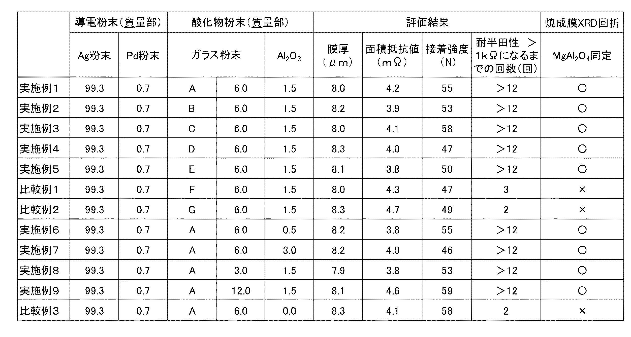
なお、実施例・比較例で用いた7種類のガラス粉末の組成比(質量%)を表1に示した。ガラス粉末A、B、C、D、Eが本発明の組成範囲に該当する一方、ガラス粉末FはMgOが含まれず、ガラス粉末GはAl2O3が含まれず、本発明の範囲外の組成である。
また、本発明の組成物の性能は、次のように厚膜導体の特性、焼成膜中のスピネルの存在によって評価した。
The composition ratio of seven glass powder used in Examples and Comparative Examples (the mass%) shown in Table 1. While glass powders A, B, C, D, and E fall within the composition range of the present invention, glass powder F does not contain MgO, and glass powder G does not contain Al 2 O 3 and is outside the scope of the present invention. It is.
The performance of the composition of the present invention was evaluated by the characteristics of the thick film conductor and the presence of spinel in the fired film as follows.
(厚膜導体の評価)
膜厚は、2.0mm×2.0mmのパッドについて、触針型の膜厚計により測定することにより評価を行った。
面積抵抗値は、幅0.5mm、長さ50mmの導体パターンの抵抗値をデジタルマルチメータにより測定して、得られた値を膜厚10μの面積抵抗値に換算することにより評価を行った。
耐半田性は、次のように評価を行った。まず、幅0.5mm、長さ50mmの焼成した厚膜導体を用いて、270℃に保持した96.5質量%Sn−3質量%Ag−0.5質量%Cu組成の鉛フリー半田浴中に、10秒間、浸した後、抵抗値を測定する操作を1回として、この操作を繰り返した。測定された抵抗値が1kΩ以上になったことにより、半田食われが起きたことを確認し、半田食われが起きるまで、すなわち測定された抵抗値が1kΩ以上となるまでの繰返し回数を計測し、耐半田性の評価とした。
接着強度は、市販のwatt浴を用い、2.0mm×2.0mmの電極パターン上に約5μ厚さのNiめっきを施し、この厚膜導体上に、直径0.65mmのSnメッキ銅線を、96.5質量%Sn−3質量%−Ag−0.5質量%Cu組成の鉛フリー半田を用いて半田付けし、垂直方向に引っ張り、剥離させ、剥離時の引っ張り力を測定することにより評価を行なった。
(Evaluation of thick film conductor)
The film thickness was evaluated by measuring a 2.0 mm × 2.0 mm pad with a stylus type film thickness meter.
The area resistance value was evaluated by measuring the resistance value of a conductor pattern having a width of 0.5 mm and a length of 50 mm with a digital multimeter, and converting the obtained value into an area resistance value having a film thickness of 10 μm.
The solder resistance was evaluated as follows. First, in a lead-free solder bath having a composition of 96.5 mass% Sn-3 mass% Ag-0.5 mass% Cu maintained at 270 ° C. using a fired thick film conductor having a width of 0.5 mm and a length of 50 mm. Then, after dipping for 10 seconds, this operation was repeated with one operation for measuring the resistance value. Confirm that the solder erosion occurred when the measured resistance value was 1 kΩ or more, and measure the number of repetitions until the solder erosion occurred, that is, until the measured resistance value became 1 kΩ or more. Evaluation of solder resistance was made.
Adhesive strength was applied to a 2.0 mm x 2.0 mm electrode pattern on a 2.0 mm x 2.0 mm electrode pattern using a commercially available watt bath, and a 0.65 mm diameter Sn-plated copper wire was applied to the thick film conductor. , soldered using lead-free solder 96.5 mass% Sn-3 mass% -Ag-0.5 mass% Cu composition, tensile vertically, is peeled off, measure the tensile force at the peeling The evaluation was performed.
(焼成膜中のスピネル)
また、実施例、比較例の組成物を用いてAl2O3基板に印刷、850℃で焼成し得られる電極膜について、XRD回折法により、焼成後電極に生成する結晶物を確認した。表1には、MgAl2O4のスピネルが同定できた場合を○、同定できた場合を×と示した。
(Spinel in the fired film)
In Examples, the Al 2 O 3 printed on the substrate, the electrode film to be obtained by firing at 850 ° C. using the composition of Comparative Example, the XRD diffraction method, it was confirmed crystals to be generated after firing electrode. In Table 1, the case where the spinel of MgAl 2 O 4 could be identified was shown as ◯, and the case where it could be identified as x.
(実施例1)
<厚膜導体形成用導体ペーストの作成>
平均粒径1.5μmの粒状Ag粉末、および平均粒径0.1μmの粒状Pd粉末からなる導電粉末に対して、表1に示した平均粒径3μmのガラス粉末A(軟化温度約800℃)と、平均粒径0.5μmのAl2O3粉とを、ターピネオール溶液にエチルセルロース樹脂を溶解して得た有機ビヒクルと混合し、3本ロールミルで混練することにより、厚膜導体形成用ペーストを作製した。
Ag粉末とPd粉末の合計を導電粉末100質量部とし、有機ビヒクルは導電粉末100質量部に対して25質量部、その他材料に関しては表2に記載した質量部のとおりで、Ag粉末とPd粉末の比率を99.3質量部+0.7質量部とし、ガラス粉末の添加量を導電粉末合計の100質量部に対して6.0質量部とし、Al2O3粉末の添加量を1.5質量部としペースト組成物を調製した。
<厚膜導体膜の形成>
作製した厚膜導体形成用ペーストを、96%アルミナ基板上にスクリーン印刷し、150℃で乾燥した。乾燥した基板を、ピーク温度850℃で9分間、トータル30分間のベルト炉で焼成し、所定のパターンの厚膜導体膜を形成した。
厚膜導体の膜厚、面積抵抗値と、前記した方法による耐半田性結果、および接着強度を表2に示す。
Example 1
<Creation of conductor paste for thick film conductor formation>
Glass powder A having an average particle size of 3 μm shown in Table 1 (softening temperature of about 800 ° C.) with respect to conductive powder composed of granular Ag powder having an average particle size of 1.5 μm and granular Pd powder having an average particle size of 0.1 μm And an Al 2 O 3 powder having an average particle size of 0.5 μm are mixed with an organic vehicle obtained by dissolving ethyl cellulose resin in a terpineol solution, and kneaded with a three-roll mill to obtain a thick film conductor forming paste. Produced.
The sum of Ag powder and Pd powder and conductive powder 100 mass parts, 25 mass parts with respect to the organic vehicle is conductive powder 100 mass parts, with respect to other materials as mass unit as described in Table 2, Ag the ratio of the powder and Pd powder and 99.3 mass parts +0.7 mass unit, and 6.0 mass parts to 100 mass parts of the conductive powder total amount of the glass powder, Al 2 O 3 the addition amount of the powder was 1.5 mass part to prepare a paste composition.
<Formation of thick film conductor film>
The produced paste for forming a thick film conductor was screen-printed on a 96% alumina substrate and dried at 150 ° C. The dried substrate was baked in a belt furnace for 9 minutes at a peak temperature of 850 ° C. for a total of 30 minutes to form a thick film conductor film having a predetermined pattern.
Table 2 shows the film thickness and sheet resistance value of the thick film conductor, the results of solder resistance by the above-described method, and the adhesive strength.
実施例1のガラスフリットAを用いて得られた厚膜導体は、12回、半田に浸しても、面積抵抗値は10Ω/□以下で、断線することは無く、耐半田性に優れていた。また、接着強度も55Nとチップ抵抗器の電極用途として十分な強度が得られていた。導体の表面を半田に濡らし、導体表面層を半田に食わさせると、その後は半田をはじくようになり、これが導体内部に析出したスピネル結晶の効果といえる。この状態にしてSEMで表面を観察すると1μ前後の粒子が確認できた。
また、表2に示す実施例1の組成物を用いてAl2O3基板に印刷、850℃で焼成し得られる電極膜について、XRD回折法により、焼成後電極に生成する結晶物を確認した。その結果、実施例1の焼成膜からは、主成分であるAgの回折ピークとともに、MgAl2O4の回折ピークが確認された。このことから本発明範囲内における組成物を用いることで、焼成過程で電極焼成体中にスピネル結晶が析出および成長していることがわかる。
The thick film conductor obtained by using the glass frit A of Example 1 was excellent in solder resistance even when immersed in solder 12 times, with a sheet resistance of 10Ω / □ or less, no disconnection. . Also, the adhesive strength was 55N, which was sufficient for use as an electrode for chip resistors. When the surface of the conductor is wetted with the solder and the surface layer of the conductor is eroded by the solder, the solder will be repelled thereafter, which can be said to be the effect of the spinel crystal deposited inside the conductor. When the surface was observed with an SEM in this state, particles of about 1 μ were confirmed.
Further, by using the composition of Example 1 shown in Table 2 printed on the Al 2 O 3 substrate, the electrode film to be obtained by firing at 850 ° C., by XRD diffraction method, it was confirmed crystals to produce a fired electrode . As a result, from the fired film of Example 1, the diffraction peak of MgAl 2 O 4 was confirmed together with the diffraction peak of Ag, which is the main component. This shows that spinel crystals are precipitated and grown in the electrode fired body during the firing process by using the composition within the scope of the present invention.
(実施例2〜5)
実施例1で用いたガラス粉末Aに代えて、同じくMgOおよびAl2O3成分を含む表1のガラス粉末B、C、D、Eを用い、同様にして、ペースト組成物を調製した。これを用いて厚膜導体を形成し、その膜厚、面積抵抗値と、前記した方法による耐半田性結果、および接着強度を調べた。
(Examples 2 to 5)
A paste composition was prepared in the same manner using the glass powders B, C, D, and E of Table 1 that also contain MgO and Al 2 O 3 components instead of the glass powder A used in Example 1. Using this, a thick film conductor was formed, and the film thickness, the sheet resistance value, the result of solder resistance by the method described above, and the adhesive strength were examined.
ガラスフリットB、C、D、Eを用いて得られた厚膜導体について評価した結果、12回、半田に浸しても、面積抵抗値は10Ω/□以下で、断線することは無く、耐半田性に優れていた。接着強度も>45Nが得られており、チップ抵抗器の電極用途として十分な強度が得られていた。
また、表2に示す実施例2〜5の組成物を用いてAl2O3基板に印刷、850℃で焼成し得られる電極膜について、XRD回折法により、焼成後電極に生成する結晶物を確認した。その結果、実施例2〜5の焼成膜からは、主成分であるAgの回折ピークとともに、MgAl2O4の回折ピークが確認された。このことから本発明範囲内における組成物を用いることで、焼成過程で電極焼成体中にスピネル結晶が析出および成長していることがわかる
As a result of evaluating the thick film conductor obtained by using the glass frit B, C, D, E, the sheet resistance is 10Ω / □ or less even if immersed in solder 12 times, and there is no disconnection, and the solder resistance It was excellent in nature. Adhesive strength was also> 45N, and sufficient strength was obtained for chip resistor electrode applications.
Furthermore, using the compositions of Examples 2-5 shown in Table 2 printed on the Al 2 O 3 substrate, the electrode film to be obtained by firing at 850 ° C., by XRD diffraction method, the crystals to be generated after firing electrode confirmed. As a result, from the fired films of Examples 2 to 5, the diffraction peak of MgAl 2 O 4 was confirmed together with the diffraction peak of Ag as the main component. From this, it can be seen that by using the composition within the scope of the present invention, spinel crystals are precipitated and grown in the electrode fired body during the firing process.
(比較例1、2)
実施例1で用いたガラス粉末Aに代えて、MgOまたはAl2O3成分を含まない表1のガラス粉末F、Gを用いた以外は同様にして、ペースト組成物を調製した。これを用いて厚膜導体を形成し、その膜厚、面積抵抗値と、前記した方法による耐半田性結果、および接着強度を調べた。
(Comparative Examples 1 and 2)
Instead of the glass powder A used in Example 1, a paste composition was prepared in the same manner except that the glass powders F and G of Table 1 not containing MgO or Al 2 O 3 components were used. Using this, a thick film conductor was formed, and the film thickness, the sheet resistance value, the result of solder resistance by the method described above, and the adhesive strength were examined.
比較例1は、本発明の組成範囲外であるガラス粉末Fを用いて評価した結果、接着強度は十分な強度が得られているが、耐半田性は、3回目の半田槽浸漬で、面積抵抗値が1kΩ以上となり、耐半田性に劣っていた。
比較例2は、本発明の組成範囲外であるガラス粉末Gを用いて評価した結果、接着強度は十分な強度が得られているが、耐半田性は、2回目の半田槽浸漬で、面積抵抗値が1kΩ以上となり、耐半田性に劣っていた。
一方、比較例1〜2のように、MgOを含まないガラス粉末Fを使用して得た導体ペースト、Al2O3を含まないガラス粉末Gを用いて得た導体ペーストの電極焼成体からはMgAl2O4の回折ピークが見られず、スピネルの結晶が析出していないことがわかった。その結果として析出結晶による半田濡れの抑制がなされず、半田槽への浸漬の繰り返しによって電極食われが進行したものと理解される。
Comparative Example 1 was evaluated using glass powder F outside the composition range of the present invention, and as a result, sufficient adhesive strength was obtained. The resistance value was 1 kΩ or more, and the solder resistance was poor.
Comparative Example 2 was evaluated using the glass powder G that is outside the composition range of the present invention, and as a result, sufficient strength was obtained. The resistance value was 1 kΩ or more, and the solder resistance was poor.
On the other hand, from Comparative Example 1-2, the electrode paste of the conductor paste obtained using the glass powder F which does not contain MgO and the glass powder G which does not contain Al 2 O 3 No diffraction peak of MgAl 2 O 4 was observed, indicating that no spinel crystals were precipitated. As a result, it is understood that solder wetting due to the precipitated crystals is not suppressed, and that electrode erosion has progressed due to repeated immersion in the solder bath.
(実施例6〜9)
実施例6、7は、実施例1において、Al2O3粉末の添加量を0.5質量部、または3.0質量部とした以外は同様にペースト組成物を作成し、評価した。
(Examples 6 to 9)
Examples 6 and 7, in Example 1, 0.5 mass part of the addition amount of Al 2 O 3 powder, or 3.0 except that the mass portion was prepared in the same manner as in the paste composition was evaluated .
その結果、12回、半田に浸しても、面積抵抗値は10Ω/□以下で、断線することは無く、耐半田性に優れていた。接着強度も>45Nが得られており、チップ抵抗器の電極用途として十分な強度が得られていた。
実施例8、9は、実施例1において、ガラス粉末Aの添加量を導電粉末合計の100質量部に対して3.0質量部または12.0質量部とした以外は同様にしてペースト組成物を作成し、評価した。その結果、12回、半田に浸しても、面積抵抗値は10Ω/□以下で、断線することは無く、耐半田性に優れていた。接着強度も>50Nが得られており、チップ抵抗器の電極用途として十分な強度が得られていた。
表2に示す実施例6〜9の組成物を用いてAl2O3基板に印刷、850℃で焼成し得られる電極膜について、XRD回折法により、焼成後電極に生成する結晶物を確認した。その結果、実施例6〜9の焼成膜からは、主成分であるAgの回折ピークとともに、MgAl2O4の回折ピークが確認された。このことから本発明範囲内における組成物を用いることで、焼成過程で電極焼成体中にスピネル結晶が析出および成長していることがわかる。
As a result, even when immersed in solder 12 times, the sheet resistance value was 10 Ω / □ or less, there was no disconnection, and the solder resistance was excellent. Adhesive strength was also> 45N, and sufficient strength was obtained for chip resistor electrode applications.
Example 8 and 9, in Example 1, except that the 3.0 mass parts or 12.0 mass parts per 100 mass parts of the conductive powder total amount of the glass powder A in the same manner A paste composition was created and evaluated. As a result, even when immersed in solder 12 times, the sheet resistance value was 10 Ω / □ or less, there was no disconnection, and the solder resistance was excellent. Adhesive strength was also> 50N, and sufficient strength was obtained for use as an electrode of a chip resistor.
About the electrode film obtained by printing on an Al 2 O 3 substrate using the compositions of Examples 6 to 9 shown in Table 2 and firing at 850 ° C., the crystalline product formed on the electrode after firing was confirmed by XRD diffraction method. . As a result, from the fired films of Examples 6 to 9, a diffraction peak of MgAl 2 O 4 was confirmed together with a diffraction peak of Ag as a main component. This shows that spinel crystals are precipitated and grown in the electrode fired body during the firing process by using the composition within the scope of the present invention.
(比較例3)
比較例3は、実施例1の組成において、Al2O3粉末を添加せずにペースト組成物を作成し、評価した。
(Comparative Example 3)
In Comparative Example 3, a paste composition was prepared and evaluated in the composition of Example 1 without adding Al 2 O 3 powder.
その結果、耐半田性に関し、2回目の半田槽浸漬で、面積抵抗値が1kΩ以上となり、耐半田性に劣っていた。一方、比較例3のように、本発明範囲内のガラス粉末Aを使用したが、酸化物粉末としてAl2O3粉末を添加しないで得た導体ペーストでは、電極焼成体からはMgAl2O4の回折ピークが見られず、スピネルの結晶が析出していないことがわかった。その結果として析出結晶による半田濡れの抑制がなされず、半田槽への浸漬の繰り返しによって電極食われが進行したものと理解される。 As a result, regarding the solder resistance, the area resistance value became 1 kΩ or more in the second solder bath immersion, and the solder resistance was poor. On the other hand, as in Comparative Example 3, the glass powder A within the scope of the present invention was used, but in the conductor paste obtained without adding Al 2 O 3 powder as the oxide powder, MgAl 2 O 4 was obtained from the electrode fired body. Thus, it was found that no spinel crystals were precipitated. As a result, it is understood that solder wetting due to the precipitated crystals is not suppressed, and that electrode erosion has progressed due to repeated immersion in the solder bath.
以上のように本発明による組成物を用いることで、半田食われが少なく、かつ、鉛を含有しない厚膜導体形成用組成物を提供することが出来、これをチップ抵抗器等の電子部品に使用すると、製品検査におけるプローブエラーによる検査歩留まり不良や、半田食われによる断線故障の少ない製品を効率よく生産できる。 As described above, by using the composition according to the present invention, it is possible to provide a composition for forming a thick film conductor that does not contain solder and contains no lead, and this can be used for an electronic component such as a chip resistor. When used, it is possible to efficiently produce a product with little inspection yield failure due to a probe error in product inspection and disconnection failure due to solder erosion.
Claims (7)
酸化物粉末(A)が、SiO2−ZnO−MgO−Al2O3系ガラス粉末(A1)と、焼成時にガラス粉末(A1)と反応してスピネル(MgAl 2 O 4 結晶)を析出するAl2O3粉末(A2)を含み、かつガラス粉末(A1)の組成比が、SiO 2 :15〜35質量%、ZnO:15〜35質量%、MgO:5〜25質量%、Al 2 O 3 :5〜20質量%の範囲であることを特徴とする厚膜導体形成用組成物。 A thick film conductor forming composition comprising a conductive powder (B), an oxide powder (A), and an organic vehicle (C),
Al in which oxide powder (A) reacts with SiO 2 —ZnO—MgO—Al 2 O 3 glass powder (A1) and glass powder (A1) during firing to precipitate spinel (MgAl 2 O 4 crystals) 2 O 3 viewed contains a powder (A2), and the composition ratio of the glass powder (A1) is, SiO 2: 15 to 35 wt%, ZnO: 15 to 35 wt%, MgO: 5 to 25 wt%, Al 2 O 3 : The composition for thick film conductor formation characterized by being the range of 5-20 mass% .
The thick film conductor according to claim 6 , wherein the applied film thickness is 20 μm or less per layer.
Priority Applications (4)
| Application Number | Priority Date | Filing Date | Title |
|---|---|---|---|
| JP2014090816A JP6201190B2 (en) | 2014-04-25 | 2014-04-25 | Thick film conductor forming composition and thick film conductor obtained using the same |
| CN201510111408.0A CN105047251B (en) | 2014-04-25 | 2015-03-13 | Compound for forming thick film conductor and the thick film conductor obtained using it |
| TW104109291A TWI647710B (en) | 2014-04-25 | 2015-03-24 | Composition for forming thick film conductor and thick film conductor using same |
| KR1020150055748A KR102265548B1 (en) | 2014-04-25 | 2015-04-21 | Composition for forming thick film conductor and thick film conductor using same |
Applications Claiming Priority (1)
| Application Number | Priority Date | Filing Date | Title |
|---|---|---|---|
| JP2014090816A JP6201190B2 (en) | 2014-04-25 | 2014-04-25 | Thick film conductor forming composition and thick film conductor obtained using the same |
Publications (2)
| Publication Number | Publication Date |
|---|---|
| JP2015210902A JP2015210902A (en) | 2015-11-24 |
| JP6201190B2 true JP6201190B2 (en) | 2017-09-27 |
Family
ID=54453728
Family Applications (1)
| Application Number | Title | Priority Date | Filing Date |
|---|---|---|---|
| JP2014090816A Active JP6201190B2 (en) | 2014-04-25 | 2014-04-25 | Thick film conductor forming composition and thick film conductor obtained using the same |
Country Status (4)
| Country | Link |
|---|---|
| JP (1) | JP6201190B2 (en) |
| KR (1) | KR102265548B1 (en) |
| CN (1) | CN105047251B (en) |
| TW (1) | TWI647710B (en) |
Families Citing this family (3)
| Publication number | Priority date | Publication date | Assignee | Title |
|---|---|---|---|---|
| US10115505B2 (en) * | 2017-02-23 | 2018-10-30 | E I Du Pont De Nemours And Company | Chip resistor |
| JP6740961B2 (en) * | 2017-05-26 | 2020-08-19 | 住友金属鉱山株式会社 | Conductor forming composition and method for producing the same, conductor and method for producing the same, chip resistor |
| CN113643840B (en) * | 2021-10-13 | 2022-03-11 | 西安宏星电子浆料科技股份有限公司 | Thick film resistor paste simultaneously suitable for alumina ceramic substrate and isolation dielectric layer |
Family Cites Families (13)
| Publication number | Priority date | Publication date | Assignee | Title |
|---|---|---|---|---|
| JPS59207853A (en) * | 1983-05-12 | 1984-11-26 | Asahi Glass Co Ltd | Glass composition |
| US4816615A (en) * | 1987-08-20 | 1989-03-28 | General Electric Company | Thick film copper conductor inks |
| JPH06223616A (en) | 1993-01-27 | 1994-08-12 | Sumitomo Metal Mining Co Ltd | Conductive paste composition |
| US5345212A (en) * | 1993-07-07 | 1994-09-06 | National Starch And Chemical Investment Holding Corporation | Power surge resistor with palladium and silver composition |
| JP3426820B2 (en) * | 1995-12-05 | 2003-07-14 | 京セラ株式会社 | Copper metallized composition and method for producing glass ceramic wiring board using the same |
| JP2004039355A (en) * | 2002-07-02 | 2004-02-05 | Sumitomo Metal Mining Co Ltd | Conductive composition |
| JP2005281010A (en) * | 2004-03-26 | 2005-10-13 | Sanyo Electric Co Ltd | Dielectric ceramic material and laminated ceramic substrate |
| JP4466402B2 (en) | 2005-02-17 | 2010-05-26 | 住友金属鉱山株式会社 | Thick film conductor composition |
| JP5488282B2 (en) * | 2010-07-13 | 2014-05-14 | 昭栄化学工業株式会社 | Conductive paste |
| JP5454414B2 (en) * | 2010-08-18 | 2014-03-26 | 住友金属鉱山株式会社 | Thick film conductor forming composition, thick film conductor formed using the composition, and chip resistor using the thick film conductor |
| WO2012043811A1 (en) * | 2010-09-30 | 2012-04-05 | 京セラ株式会社 | Conductive paste for use in photovoltaic cell and method of producing photovoltaic cell element using the same |
| ZA201208302B (en) * | 2011-11-09 | 2014-10-29 | Heraeus Precious Metals Gmbh | Thick film conductive composition and use thereof |
| US9029692B2 (en) * | 2012-04-17 | 2015-05-12 | Heraeus Precious Metals North America Conshohocken Llc | Tellurium inorganic reaction systems for conductive thick film paste for solar cell contacts |
-
2014
- 2014-04-25 JP JP2014090816A patent/JP6201190B2/en active Active
-
2015
- 2015-03-13 CN CN201510111408.0A patent/CN105047251B/en active Active
- 2015-03-24 TW TW104109291A patent/TWI647710B/en active
- 2015-04-21 KR KR1020150055748A patent/KR102265548B1/en active IP Right Grant
Also Published As
| Publication number | Publication date |
|---|---|
| KR102265548B1 (en) | 2021-06-17 |
| CN105047251A (en) | 2015-11-11 |
| TW201541467A (en) | 2015-11-01 |
| KR20150123725A (en) | 2015-11-04 |
| CN105047251B (en) | 2018-11-16 |
| JP2015210902A (en) | 2015-11-24 |
| TWI647710B (en) | 2019-01-11 |
Similar Documents
| Publication | Publication Date | Title |
|---|---|---|
| JP4466402B2 (en) | Thick film conductor composition | |
| JP5454414B2 (en) | Thick film conductor forming composition, thick film conductor formed using the composition, and chip resistor using the thick film conductor | |
| JP4600282B2 (en) | Conductive paste | |
| KR101172723B1 (en) | Copper conductor paste, conductor circuit board and electronic part | |
| KR101786722B1 (en) | Conductive paste | |
| KR102292562B1 (en) | conductive paste | |
| TW201511036A (en) | Thick print copper pastes for aluminum nitride substrates | |
| WO2012114673A1 (en) | Chip resistor and method of producing same | |
| JP6201190B2 (en) | Thick film conductor forming composition and thick film conductor obtained using the same | |
| JP5673515B2 (en) | Thick film conductor forming composition, thick film conductor using the same, and method for producing the same | |
| KR102441705B1 (en) | Conductive paste for forming external electrodes of multilayer ceramic electronic components | |
| JP6769208B2 (en) | Lead-free conductive paste | |
| TW201701299A (en) | Cu paste composition for forming thick film conductor, and thick film conductor | |
| JP5556518B2 (en) | Conductive paste | |
| CN109994246B (en) | Powder composition for forming thick-film conductor and slurry for forming thick-film conductor | |
| TWI796400B (en) | Powder composition for forming thick film conductor and paste for forming thick film conductor | |
| JP2022082004A (en) | Powder composition for forming thick conductor, paste for forming thick conductor, and thick conductor | |
| JP2019032993A (en) | Thick conductor forming composition and method for producing thick conductor | |
| JP2019110105A5 (en) |
Legal Events
| Date | Code | Title | Description |
|---|---|---|---|
| A621 | Written request for application examination |
Free format text: JAPANESE INTERMEDIATE CODE: A621 Effective date: 20160419 |
|
| A131 | Notification of reasons for refusal |
Free format text: JAPANESE INTERMEDIATE CODE: A131 Effective date: 20170131 |
|
| A977 | Report on retrieval |
Free format text: JAPANESE INTERMEDIATE CODE: A971007 Effective date: 20170131 |
|
| A521 | Written amendment |
Free format text: JAPANESE INTERMEDIATE CODE: A523 Effective date: 20170323 |
|
| A131 | Notification of reasons for refusal |
Free format text: JAPANESE INTERMEDIATE CODE: A131 Effective date: 20170620 |
|
| A521 | Written amendment |
Free format text: JAPANESE INTERMEDIATE CODE: A523 Effective date: 20170703 |
|
| TRDD | Decision of grant or rejection written | ||
| A01 | Written decision to grant a patent or to grant a registration (utility model) |
Free format text: JAPANESE INTERMEDIATE CODE: A01 Effective date: 20170725 |
|
| A61 | First payment of annual fees (during grant procedure) |
Free format text: JAPANESE INTERMEDIATE CODE: A61 Effective date: 20170807 |
|
| R150 | Certificate of patent or registration of utility model |
Ref document number: 6201190 Country of ref document: JP Free format text: JAPANESE INTERMEDIATE CODE: R150 |