JP6189933B2 - Method and system for critical dimension uniformity using charged particle beam lithography - Google Patents
Method and system for critical dimension uniformity using charged particle beam lithography Download PDFInfo
- Publication number
- JP6189933B2 JP6189933B2 JP2015507093A JP2015507093A JP6189933B2 JP 6189933 B2 JP6189933 B2 JP 6189933B2 JP 2015507093 A JP2015507093 A JP 2015507093A JP 2015507093 A JP2015507093 A JP 2015507093A JP 6189933 B2 JP6189933 B2 JP 6189933B2
- Authority
- JP
- Japan
- Prior art keywords
- shot
- pattern
- shots
- charged particle
- particle beam
- Prior art date
- Legal status (The legal status is an assumption and is not a legal conclusion. Google has not performed a legal analysis and makes no representation as to the accuracy of the status listed.)
- Active
Links
- 238000000034 method Methods 0.000 title claims description 90
- 238000002039 particle-beam lithography Methods 0.000 title claims description 17
- 239000002245 particle Substances 0.000 claims description 47
- 230000000694 effects Effects 0.000 claims description 43
- 238000004519 manufacturing process Methods 0.000 claims description 35
- 230000008569 process Effects 0.000 claims description 32
- 238000012937 correction Methods 0.000 claims description 20
- 238000004088 simulation Methods 0.000 claims description 20
- 238000002360 preparation method Methods 0.000 claims description 11
- 230000009467 reduction Effects 0.000 claims description 8
- 238000000342 Monte Carlo simulation Methods 0.000 claims description 6
- 239000000758 substrate Substances 0.000 description 53
- 238000010894 electron beam technology Methods 0.000 description 33
- 238000013461 design Methods 0.000 description 32
- 235000012431 wafers Nutrition 0.000 description 29
- 238000000206 photolithography Methods 0.000 description 26
- 238000005457 optimization Methods 0.000 description 21
- 238000001459 lithography Methods 0.000 description 19
- 238000009826 distribution Methods 0.000 description 18
- 238000012545 processing Methods 0.000 description 18
- 238000004364 calculation method Methods 0.000 description 13
- XUIMIQQOPSSXEZ-UHFFFAOYSA-N Silicon Chemical compound [Si] XUIMIQQOPSSXEZ-UHFFFAOYSA-N 0.000 description 10
- 229910052710 silicon Inorganic materials 0.000 description 10
- 239000010703 silicon Substances 0.000 description 10
- 238000002474 experimental method Methods 0.000 description 9
- 230000003287 optical effect Effects 0.000 description 8
- 238000011161 development Methods 0.000 description 7
- 230000006872 improvement Effects 0.000 description 7
- 238000010586 diagram Methods 0.000 description 6
- 238000012986 modification Methods 0.000 description 6
- 230000004048 modification Effects 0.000 description 6
- 230000002829 reductive effect Effects 0.000 description 6
- 230000000903 blocking effect Effects 0.000 description 5
- 238000005516 engineering process Methods 0.000 description 5
- 238000005259 measurement Methods 0.000 description 5
- 239000004065 semiconductor Substances 0.000 description 5
- 238000012546 transfer Methods 0.000 description 5
- 238000012795 verification Methods 0.000 description 5
- 230000008859 change Effects 0.000 description 4
- 238000005530 etching Methods 0.000 description 4
- 230000006870 function Effects 0.000 description 4
- 238000007781 pre-processing Methods 0.000 description 4
- 238000004458 analytical method Methods 0.000 description 3
- 238000013459 approach Methods 0.000 description 3
- 238000005034 decoration Methods 0.000 description 3
- 230000007423 decrease Effects 0.000 description 3
- 238000009792 diffusion process Methods 0.000 description 3
- 238000001127 nanoimprint lithography Methods 0.000 description 3
- 230000035945 sensitivity Effects 0.000 description 3
- 238000011960 computer-aided design Methods 0.000 description 2
- 238000010276 construction Methods 0.000 description 2
- 238000007796 conventional method Methods 0.000 description 2
- 238000001900 extreme ultraviolet lithography Methods 0.000 description 2
- 238000012805 post-processing Methods 0.000 description 2
- 238000012935 Averaging Methods 0.000 description 1
- 238000001015 X-ray lithography Methods 0.000 description 1
- 230000004075 alteration Effects 0.000 description 1
- 239000011248 coating agent Substances 0.000 description 1
- 238000000576 coating method Methods 0.000 description 1
- 238000012790 confirmation Methods 0.000 description 1
- 238000003384 imaging method Methods 0.000 description 1
- 230000003993 interaction Effects 0.000 description 1
- 238000005468 ion implantation Methods 0.000 description 1
- 230000001678 irradiating effect Effects 0.000 description 1
- 230000000670 limiting effect Effects 0.000 description 1
- 230000000873 masking effect Effects 0.000 description 1
- 239000000463 material Substances 0.000 description 1
- 230000007246 mechanism Effects 0.000 description 1
- 239000002184 metal Substances 0.000 description 1
- 238000001465 metallisation Methods 0.000 description 1
- 230000008450 motivation Effects 0.000 description 1
- 230000001151 other effect Effects 0.000 description 1
- 238000013021 overheating Methods 0.000 description 1
- 230000003647 oxidation Effects 0.000 description 1
- 238000007254 oxidation reaction Methods 0.000 description 1
- 230000036961 partial effect Effects 0.000 description 1
- 229920002120 photoresistant polymer Polymers 0.000 description 1
- 230000000704 physical effect Effects 0.000 description 1
- 238000005498 polishing Methods 0.000 description 1
- 238000007639 printing Methods 0.000 description 1
- 230000005855 radiation Effects 0.000 description 1
- 230000003252 repetitive effect Effects 0.000 description 1
- 230000002441 reversible effect Effects 0.000 description 1
- 238000001338 self-assembly Methods 0.000 description 1
- 230000009897 systematic effect Effects 0.000 description 1
Images


Classifications
-
- G—PHYSICS
- G06—COMPUTING; CALCULATING OR COUNTING
- G06F—ELECTRIC DIGITAL DATA PROCESSING
- G06F30/00—Computer-aided design [CAD]
-
- H—ELECTRICITY
- H01—ELECTRIC ELEMENTS
- H01L—SEMICONDUCTOR DEVICES NOT COVERED BY CLASS H10
- H01L21/00—Processes or apparatus adapted for the manufacture or treatment of semiconductor or solid state devices or of parts thereof
- H01L21/02—Manufacture or treatment of semiconductor devices or of parts thereof
- H01L21/027—Making masks on semiconductor bodies for further photolithographic processing not provided for in group H01L21/18 or H01L21/34
- H01L21/0271—Making masks on semiconductor bodies for further photolithographic processing not provided for in group H01L21/18 or H01L21/34 comprising organic layers
- H01L21/0273—Making masks on semiconductor bodies for further photolithographic processing not provided for in group H01L21/18 or H01L21/34 comprising organic layers characterised by the treatment of photoresist layers
- H01L21/0274—Photolithographic processes
- H01L21/0275—Photolithographic processes using lasers
-
- G—PHYSICS
- G03—PHOTOGRAPHY; CINEMATOGRAPHY; ANALOGOUS TECHNIQUES USING WAVES OTHER THAN OPTICAL WAVES; ELECTROGRAPHY; HOLOGRAPHY
- G03F—PHOTOMECHANICAL PRODUCTION OF TEXTURED OR PATTERNED SURFACES, e.g. FOR PRINTING, FOR PROCESSING OF SEMICONDUCTOR DEVICES; MATERIALS THEREFOR; ORIGINALS THEREFOR; APPARATUS SPECIALLY ADAPTED THEREFOR
- G03F1/00—Originals for photomechanical production of textured or patterned surfaces, e.g., masks, photo-masks, reticles; Mask blanks or pellicles therefor; Containers specially adapted therefor; Preparation thereof
- G03F1/36—Masks having proximity correction features; Preparation thereof, e.g. optical proximity correction [OPC] design processes
-
- G—PHYSICS
- G03—PHOTOGRAPHY; CINEMATOGRAPHY; ANALOGOUS TECHNIQUES USING WAVES OTHER THAN OPTICAL WAVES; ELECTROGRAPHY; HOLOGRAPHY
- G03F—PHOTOMECHANICAL PRODUCTION OF TEXTURED OR PATTERNED SURFACES, e.g. FOR PRINTING, FOR PROCESSING OF SEMICONDUCTOR DEVICES; MATERIALS THEREFOR; ORIGINALS THEREFOR; APPARATUS SPECIALLY ADAPTED THEREFOR
- G03F1/00—Originals for photomechanical production of textured or patterned surfaces, e.g., masks, photo-masks, reticles; Mask blanks or pellicles therefor; Containers specially adapted therefor; Preparation thereof
- G03F1/68—Preparation processes not covered by groups G03F1/20 - G03F1/50
- G03F1/70—Adapting basic layout or design of masks to lithographic process requirements, e.g., second iteration correction of mask patterns for imaging
Landscapes
- Physics & Mathematics (AREA)
- Engineering & Computer Science (AREA)
- General Physics & Mathematics (AREA)
- Computer Hardware Design (AREA)
- Theoretical Computer Science (AREA)
- Condensed Matter Physics & Semiconductors (AREA)
- Manufacturing & Machinery (AREA)
- Microelectronics & Electronic Packaging (AREA)
- Power Engineering (AREA)
- Evolutionary Computation (AREA)
- Geometry (AREA)
- General Engineering & Computer Science (AREA)
- Optics & Photonics (AREA)
- Exposure And Positioning Against Photoresist Photosensitive Materials (AREA)
- Electron Beam Exposure (AREA)
- Architecture (AREA)
- Software Systems (AREA)
- Preparing Plates And Mask In Photomechanical Process (AREA)
Description
関連出願
この出願は、「可変成形ビームリソグラフィを用いて限界寸法均一性を改善する方法およびシステム(Method And System For Improving Critical Dimension Uniformity Using Variable Shaped Beam Lithography)」と題される、2012年4月18日に提出された米国仮特許出願第61/625,932号からの優先権を主張し;1)2013年4月15日に提出された、「荷電粒子ビームリソグラフィを用いてパターンを形成する方法およびシステム(Method and System For Forming Patterns Using Charged Particle Beam Lithography)」と題されるFujimuraの米国特許出願第13/862,471号;2)2013年4月15日に提出された、「荷電粒子ビームリソグラフィを用いてパターンを形成する方法およびシステム(Method and System For Forming Patterns Using Charged Particle Beam Lithography)」と題されるFujimuraの米国特許出願第13/862,472号;3)2013年4月15日に提出された、「荷電粒子ビームリソグラフィを用いてパターンを形成する方法およびシステム(Method and System For Forming Patterns Using Charged Particle Beam Lithography)」と題されるFujimuraの米国特許出願第13/862,475号;4)2013年4月15日に提出された、「荷電粒子ビームリソグラフィを用いる限界寸法均一性のための方法およびシステム(Method And System For Critical Dimension Uniformity Using Charged Particle Beam Lithography)」と題される米国特許出願第13/862,476号;および5)「光学リソグラフィを用いて製造される基板上における像の最適化のための方法およびシステム(Method And System For Optimization Of An Image On A Substrate To Be Manufactured Using Optical Lithography)」と題される、2013年3月21日に公開された米国特許公開第2013/0070222号に関連し;それらのすべてをすべての目的のためにここに引用により援用する。
Related Application This application is entitled “Method and System For Improving Critical Dimension Uniformity Using Variable Shaped Beam Lithography”, April 18, 2012. Claiming priority from US Provisional Patent Application No. 61 / 625,932 filed on the same day; 1) “Method of forming a pattern using charged particle beam lithography, filed on April 15, 2013” Fujimura US Patent Application No. 13 / 862,471 entitled "Method and System For Forming Patterns Using Charged Particle Beam Lithography"; 2) "Charged Particle Beam" filed April 15, 2013; Method and System for Forming Patterns Using Charged Particle Beam Lithography " US Patent Application No. 13 / 862,472, entitled Fujimura, entitled “Method and System For: Patterned Using Charged Particle Beam Lithography” filed on April 15, 2013. Fujimura US Patent Application No. 13 / 862,475 entitled "Forming Patterns Using Charged Particle Beam Lithography"; 4) "Limited Dimension Uniformity Using Charged Particle Beam Lithography" US Patent Application No. 13 / 862,476 entitled “Method And System For Critical Dimension Uniformity Using Charged Particle Beam Lithography”; and 5) “On a Substrate Manufactured Using Optical Lithography” Method and System For Optimization Of An Image On A Substrate To Be Manufactured Using Optic al. Lithography), published on March 21, 2013, which is hereby incorporated by reference for all purposes.
開示の背景
集積回路といった半導体装置を作製または製造する際、光学リソグラフィを用いて半導体装置を製造することができる。光学リソグラフィとは、レチクルから製造されたリソグラフィマスクまたはフォトマスクを用いてパターンを半導体またはシリコンウェハなどの基板に転写して集積回路(I.C.)を作成する印刷処理である。他の基板は、フラットパネルディスプレイ、ホログラフィマスクまたは他のレチクルをも含むことができる。従来の光学リソグラフィは193nmの波長を有する光源を用いるが、極紫外線(EUV)またはX線リソグラフィも本願においては光学リソグラフィの一種であると考えられる。1つのレチクルまたは複数のレチクルは、集積回路の個別の層に対応する回路パターンを含むことができ、このパターンを、フォトレジストまたはレジストとして知られている放射感応材の層で被覆された基板の特定領域上に結像できる。パターン化された層が転写されると、その層はエッチング、イオン注入(ドーピング)、金属化、酸化、および研磨といったさまざまな他の処理を受ける。これらの処理を用いて基板に個別の層を仕上げる。複数の層が必要である場合、その処理全体またはその変形などがそれぞれの新しい層に対して繰返される。最終的には、複数の装置または集積回路の組合せが、基板上に存在することになる。これら集積回路は、ダイシングまたはソーイングにより互いに分離され、個々のパッケージに取付けられてもよい。より一般的な場合、基板上のパターンを用いて、ディスプレイ画素、ホログラム、誘導自己組織化(DSA)ガードバンド、または磁気記録ヘッドといった加工品を規定してもよい。従来の光学リソグラフィ書込装置は、典型的には、光学リソグラフィプロセスの際フォトマスクパターンを4分の1に減少させる。したがって、レチクルまたはマスクに形成されるパターンは、基板またはウェハ上の所望のパターンの大きさよりも4倍大きくなければならない。
BACKGROUND OF THE DISCLOSURE When manufacturing or manufacturing a semiconductor device such as an integrated circuit, the semiconductor device can be manufactured using optical lithography. Optical lithography is a printing process in which an integrated circuit (IC) is created by transferring a pattern to a substrate such as a semiconductor or silicon wafer using a lithography mask or a photomask manufactured from a reticle. Other substrates can also include flat panel displays, holographic masks or other reticles. Conventional optical lithography uses a light source having a wavelength of 193 nm, but extreme ultraviolet (EUV) or X-ray lithography is also considered a type of optical lithography in this application. The reticle or reticles can include circuit patterns corresponding to individual layers of the integrated circuit, and this pattern can be applied to a substrate coated with a layer of radiation-sensitive material known as photoresist or resist. An image can be formed on a specific area. Once the patterned layer is transferred, it undergoes various other processes such as etching, ion implantation (doping), metallization, oxidation, and polishing. These processes are used to finish individual layers on the substrate. If multiple layers are required, the entire process or variations thereof are repeated for each new layer. Eventually, a combination of multiple devices or integrated circuits will be present on the substrate. These integrated circuits may be separated from each other by dicing or sawing and attached to individual packages. In the more general case, the pattern on the substrate may be used to define a workpiece such as a display pixel, hologram, guided self-assembly (DSA) guard band, or magnetic recording head. Conventional optical lithographic writing devices typically reduce the photomask pattern by a factor of four during the optical lithography process. Therefore, the pattern formed on the reticle or mask must be four times larger than the desired pattern size on the substrate or wafer.
集積回路といった半導体装置の作製または製造において、非光学的方法を用いてリソグラフィマスク上のパターンをシリコンウェハなどの基板に転写することもできる。このような非光学リソグラフィプロセスの一例はナノインプリントリソグラフィ(NIL)である。ナノインプリントリソグラフィにおいては、リソグラフィマスクを表面に接触させることにより、リソグラフィマスクパターンが表面に転写される。 In manufacturing or manufacturing a semiconductor device such as an integrated circuit, a pattern on a lithography mask can be transferred to a substrate such as a silicon wafer by using a non-optical method. One example of such a non-optical lithography process is nanoimprint lithography (NIL). In nanoimprint lithography, a lithography mask pattern is transferred to a surface by bringing the lithography mask into contact with the surface.
荷電粒子ビームリソグラフィの2つの一般的な種類として、可変成形ビーム(VSB)およびキャラクタ投影(CP)がある。これらは、両方とも成形ビーム荷電粒子ビームリソグラフィの下位カテゴリであり、精密な電子ビームが成形されて動かされ、ウェハの表面またはレチクルの表面といった、レジストが被覆されている表面を露光する。VSBにおいて、これらの形は単純な形であり、通常は、特定の最小および最大サイズを有し、側辺がデカルト座標面の軸に平行である矩形(すなわち「マンハッタン」配向)、ならびに特定の最小および最大サイズを有する45度の直角三角形(すなわち3つの内角が45度、45度および90度である三角形)に限定されている。特定の場所において、電子の線量がこれら単純な形でレジストに射出される。この種のシステムでの合計書込時間は、そのショット数に応じて長くなる。キャラクタ投影(CP)において、システムにステンシルが使用され、ステンシルは中にさまざまなアパーチャやキャラクタを有し、その形は直線の、任意の角度の付いた線形の、円形の、略円形の、環状の、略環状の、楕円形の、略楕円形の、部分的に円形の、部分的に略円形の、部分的に環状の、部分的に略環状の、部分的に略楕円形の、または任意の曲線の、複雑な形であり得、さらに接続された一組の複雑な形、または接続された一組の複雑な形の繋がってない複数の組のグループであり得る。電子ビームはステンシルにあるキャラクタを通って射出されて、レチクル上により複雑なパターンを効率よくもたらす。理論的に、このようなシステムはVSBシステムよりも速く、なぜなら、各々の時間のかかるショットにおいてより複雑な形を射出することができるからである。こうして、VSBシステムで射出されたE字型のパターンは4回のショットが必要であるのに対して、同じE字型のパターンはキャラクタ投影システムでは1回のショットで射出することができる。VSBシステムはキャラクタ投影の特殊な(簡単な)事例であると考えることができ、キャラクタは簡単なキャラクタだけ、通常は矩形または45−45−90度の三角形である。さらに、あるキャラクタを部分的に露光することもできる。これは、たとえば粒子ビームの一部をブロックすることによって行なうことができる。たとえば、上記のE字型のパターンは、ビームの異なる部分をアパーチャによって遮断することにより、F字型のパターンまたはI字型のパターンとして部分的に露光することができる。これはVSBを用いてさまざまな大きさの矩形を射出できるのと同じ原理である。本開示において、部分的投影はキャラクタ投影およびVSB投影の両方を意味するように用いられる。成形ビーム荷電粒子ビームリソグラフィは、単一の成形ビームを用いてもよく、または単一の成形ビームより速い書込速度を生じさせ、同時に表面を露光する、複数の成形ビームを用いてもよい。 Two common types of charged particle beam lithography are variable shaped beam (VSB) and character projection (CP). These are both subcategories of shaped beam charged particle beam lithography where a precision electron beam is shaped and moved to expose a resist-coated surface, such as the surface of a wafer or the surface of a reticle. In VSB, these shapes are simple shapes, usually a rectangle with a certain minimum and maximum size, with the sides parallel to the axis of the Cartesian coordinate plane (ie, a “Manhattan” orientation), and a certain Limited to 45 degree right triangles with minimum and maximum sizes (ie, triangles with 3 interior angles of 45, 45 and 90 degrees). At certain locations, a dose of electrons is injected into the resist in these simple forms. The total writing time in this type of system increases with the number of shots. In character projection (CP), a stencil is used in the system, the stencil has various apertures and characters in it, the shape is linear, linear at any angle, circular, nearly circular, annular Substantially annular, oval, substantially oval, partially circular, partially approximately circular, partially annular, partially approximately annular, partially approximately oval, or It can be a complex shape of any curve, and can also be a connected set of complex shapes, or a set of connected complex shapes of multiple unconnected groups. The electron beam is ejected through the character in the stencil to efficiently produce a more complex pattern on the reticle. Theoretically, such a system is faster than a VSB system because it can fire a more complex shape in each time-consuming shot. Thus, while the E-shaped pattern emitted by the VSB system requires four shots, the same E-shaped pattern can be emitted by one shot in the character projection system. The VSB system can be considered a special (simple) case of character projection, where the character is only a simple character, usually a rectangle or a 45-45-90 degree triangle. Furthermore, a certain character can be partially exposed. This can be done, for example, by blocking a part of the particle beam. For example, the E-shaped pattern described above can be partially exposed as an F-shaped pattern or an I-shaped pattern by blocking different portions of the beam with an aperture. This is the same principle that rectangles of various sizes can be emitted using VSB. In this disclosure, partial projection is used to mean both character projection and VSB projection. Shaped beam charged particle beam lithography may use a single shaped beam, or it may use multiple shaped beams that produce a faster writing speed and simultaneously expose the surface than a single shaped beam.
上記のように、リソグラフィにおいて、リソグラフィマスクまたはレチクルは、基板に集積する回路コンポーネントに対応する幾何学的パターンを含む。レチクルを製造するために用いられるパターンは、コンピュータ支援設計(CAD)ソフトウェアまたはプログラムを用いて生成することができる。これらパターンを設計する際、CADプログラムはレチクルを製造するために一連の所定のデザインルールに従い得る。これらのルールは加工、設計、および最終用途制限事項によって設定される。最終用途制限事項の一例は、規定の供給電圧では十分に動作できない態様でトランジスタのジオメトリを規定することである。特に、デザインルールは回路装置または配線間の間隔公差を規定することができる。デザインルールは、たとえば回路装置または配線が不所望な態様で互いに影響しないようにするために用いられる。たとえば、デザインルールを用いて、配線が短絡を引起さないように、互いに近くあり過ぎないようにする。デザインルールの制限は、とりわけ確実に製造できる最小寸法を反映する。この最小寸法に言及する場合、通常は限界寸法の概念が導入される。これらは、たとえば1本の配線の最小幅、または2本の配線間の最小間隔として規定され、このような寸法は微妙な制御を必要とする。 As described above, in lithography, a lithographic mask or reticle includes a geometric pattern that corresponds to a circuit component integrated on a substrate. The pattern used to manufacture the reticle can be generated using computer aided design (CAD) software or programs. In designing these patterns, the CAD program can follow a set of predetermined design rules to produce a reticle. These rules are set by processing, design, and end use restrictions. An example of an end use limitation is to define the transistor geometry in such a way that it cannot operate satisfactorily with a specified supply voltage. In particular, the design rules can define the spacing tolerance between circuit devices or wiring. Design rules are used, for example, to prevent circuit devices or wiring from affecting each other in an undesired manner. For example, design rules are used to prevent wires from being too close to each other so as not to cause a short circuit. The design rule limitations particularly reflect the smallest dimensions that can be reliably manufactured. When referring to this minimum dimension, the concept of critical dimension is usually introduced. These are defined as, for example, the minimum width of one wire or the minimum distance between two wires, and such dimensions require delicate control.
光学リソグラフィによる集積回路の製造の1つの目標は、レチクルを用いて当初の回路デザインを基板上に再現することである。集積回路の製造者は常にできるだけ有効に半導体ウェハの領域を使用することを試みる。技術者は回路の大きさをできるだけ縮小して集積回路がより多くの回路素子を含み、かつ消費電力を減らすようにしている。集積回路の限界寸法の大きさが小さくなり、回路密度が増加すると、回路パターンまたは物理的デザインの限界寸法は、従来の光学リソグラフィで用いられる光学露光ツールの解像限界に近づく。回路パターンの限界寸法がより小さくなって露光ツールの解像度に近づくと、物理的デザインをレジスト層上で現像される実際の回路パターンに正確に転写することは困難になる。光学リソグラフィをさらに用いて、光学リソグラフィプロセスで用いられる光の波長よりも小さいフィーチャを有するパターンを転写するために、光近接効果補正(OPC)として知られる処理が開発された。OPCは光回折およびフィーチャが近接したフィーチャと光学的に相互作用するといった作用によって引起される歪みを補償するために、物理的デザインを変える。OPCはレチクルで行なわれる解像度向上技術すべてを含む。 One goal of manufacturing integrated circuits by optical lithography is to reproduce the original circuit design on the substrate using a reticle. Integrated circuit manufacturers always try to use areas of the semiconductor wafer as effectively as possible. Engineers reduce the size of the circuit as much as possible so that the integrated circuit includes more circuit elements and reduces power consumption. As the critical dimension size of integrated circuits decreases and circuit density increases, the critical dimension of circuit patterns or physical designs approaches the resolution limit of optical exposure tools used in conventional optical lithography. As the critical dimension of the circuit pattern becomes smaller and approaches the resolution of the exposure tool, it becomes difficult to accurately transfer the physical design to the actual circuit pattern developed on the resist layer. A process known as optical proximity correction (OPC) has been developed to further use optical lithography to transfer patterns having features smaller than the wavelength of light used in the optical lithography process. OPC changes the physical design to compensate for distortions caused by light diffraction and the effect that features interact optically with nearby features. OPC includes all resolution enhancement techniques performed on the reticle.
OPCはサブ解像度リソグラフィックフィーチャをマスクパターンに加えて、当初の物理的デザインパターン、すなわちデザインと、基板に転写された最終回路パターンとの差を減らす。サブ解像度リソグラフィックフィーチャは、物理的デザインの当初のパターンと相互作用し、およびフィーチャ同士で相互作用し、近接効果を補償して、最終の転写された回路パターンを向上させる。パターンの転写を向上するために用いられる1つのフィーチャは、サブ解像度アシストフィーチャ(SRAF)である。パターン転写を向上させるために加えられる別のフィーチャは「セリフ」と呼ばれる。セリフはパターンの内側または外側の角に位置付けることができる小さなフィーチャであって、最終の転写された像の角を先鋭にする。SRAFでの表面製造処理に求められる精度は、しばしばメインフィーチャと呼ばれる、基板上に印刷するよう意図されるパターンに求められる精度よりも低い。セリフはメインフィーチャの一部である。光学リソグラフィの限界がサブ波長制度に大きく拡張されるにつれ、より微妙な相互作用および作用を補償するために、OPCフィーチャはますます複雑にならなければならない。結像システムがその限界近くになるにつれ、十分に微細なOPCフィーチャを有するレチクルを作成できることは重要となる。セリフや他のOPCフィーチャをマスクパターンに加えることは有利であるが、これはマスクパターンでの総フィーチャ数を実質的に増加させる。たとえば、従来の技術を用いて正方形の各角にセリフを加えることは、マスクまたはレチクルパターンにさらに8個の矩形を加えることになる。OPCフィーチャを加えることは労力のいる作業であり、貴重な演算時間を必要とし、結果的にはレチクルは高価なものになる。OPCパターンは複雑であるばかりでなく、光近接効果は最小のラインアンドスペース寸法と比べて長距離のものなので、所与の場所での正確なOPCパターンは、近くに他のどのようなジオメトリがあるかに著しく依存する。こうして、たとえば線の端部は、レチクル上で何が近くにあるかに応じて、異なる大きさのセリフを有することになる。これは全く同じ形をウェハ上に製造することが目的であったとしても、同様である。このような若干の、しかし臨界的なばらつきは重要であり、他のものがレチクルパターンを形成できることを妨げていた。レチクルに書込まれるべきOPC装飾パターンは、デザインされたフィーチャ、すなわちOPC装飾前のデザインを反映するフィーチャと、セリフ、ジョグおよびSRAFを含み得るOPCフィーチャとに基づいて論じるのが従来的である。若干のばらつきとは何を意味するかを定量化すると、近傍同士のOPC装飾の典型的な若干のばらつきは、デザインされたフィーチャサイズの5%から80%であり得る。確認のために記載しているが、ここで言及しているのは、OPCのデザインのばらつきである。ラインエッジ粗さおよび角の丸みといった製造上のばらつきも、実際の表面パターンに存在することになる。これらのOPCばらつきが実質的に同じパターンをウェハ上にもたらす場合、ウェハのジオメトリは、たとえばトランジスタまたは配線などの、ジオメトリが実行するように設計される機能の詳細に依存する所定誤差内で同一であることが目標とされることを意味する。しかしながら、典型的な仕様はデザインされたフィーチャ範囲の2%から50%にある。ばらつきを引起す製造要因はたくさんあるが、全体の誤差のOPC成分は上記範囲内にあることが多い。サブ解像度アシストフィーチャといったOPCの形状は、さまざまなデザインルール、たとえば光学リソグラフィを用いてウェハに転写することができる最も小さいフィーチャのサイズに基づくルールに従う。他のデザインルールは、マスク製造処理によるものであるか、またはレチクル上にパターンを形成するためにキャラクタ投影荷電粒子ビーム書込システムが用いられているのなら、ステンシル製造処理によるものである。さらに、マスク上のSRAFフィーチャの精度の要件は、マスク上のデザインされたフィーチャの精度の要件よりも低いこともあり得る。処理ノードが小さくなるにつれ、フォトマスク上の最も小さいSRAFのサイズも小さくなる。たとえば、20nmロジック処理ノードでは、最も高い精度の層に対してはマスクに40nmから60nmのSRAFが必要である。 OPC adds sub-resolution lithographic features to the mask pattern to reduce the difference between the original physical design pattern, ie the design, and the final circuit pattern transferred to the substrate. The sub-resolution lithographic features interact with the original pattern of the physical design and interact with each other to compensate for proximity effects and improve the final transferred circuit pattern. One feature used to improve pattern transfer is the sub-resolution assist feature (SRAF). Another feature added to improve pattern transfer is called "serif". Serifs are small features that can be located at the inside or outside corners of the pattern and sharpen the corners of the final transferred image. The accuracy required for surface fabrication processes in SRAF is lower than that required for patterns intended to be printed on a substrate, often referred to as main features. Serif is part of the main feature. As the limits of optical lithography are greatly extended to subwavelength regimes, OPC features must become increasingly complex to compensate for more subtle interactions and effects. As the imaging system approaches its limit, it becomes important to be able to create reticles with sufficiently fine OPC features. While it is advantageous to add serifs and other OPC features to the mask pattern, this substantially increases the total number of features in the mask pattern. For example, adding a serif to each corner of a square using conventional techniques adds eight more rectangles to the mask or reticle pattern. Adding OPC features is a laborious task, requires valuable computation time, and results in expensive reticles. Not only is the OPC pattern complex, but the optical proximity effect is long distance compared to the smallest line and space dimensions, so the exact OPC pattern at a given location is not close to any other geometry. It depends heavily on what it is. Thus, for example, the end of a line will have different sized lines depending on what is nearby on the reticle. This is true even if the goal is to produce exactly the same shape on the wafer. These slight but critical variations are important and have prevented others from being able to form reticle patterns. OPC decoration patterns to be written on the reticle are traditionally discussed based on designed features, i.e., features that reflect the design prior to OPC decoration, and OPC features that may include serifs, jogs, and SRAFs. Quantifying what the slight variation means, the typical slight variation in neighborhood OPC decoration can be between 5% and 80% of the designed feature size. Although described for confirmation, it is here that OPC design variation is mentioned. Manufacturing variations such as line edge roughness and corner roundness will also be present in the actual surface pattern. If these OPC variations result in substantially the same pattern on the wafer, the wafer geometry is the same within a predetermined error that depends on the details of the function that the geometry is designed to perform, such as, for example, a transistor or wiring. It means that there is a goal. However, typical specifications are 2% to 50% of the designed feature range. There are many manufacturing factors that cause variations, but the OPC component of the overall error is often within the above range. OPC shapes, such as sub-resolution assist features, follow various design rules, such as those based on the size of the smallest feature that can be transferred to a wafer using optical lithography. Other design rules are due to the mask manufacturing process or, if a character projection charged particle beam writing system is used to form a pattern on the reticle, to a stencil manufacturing process. In addition, the accuracy requirements of the SRAF features on the mask may be lower than the accuracy requirements of the designed features on the mask. As the processing node gets smaller, the size of the smallest SRAF on the photomask also gets smaller. For example, a 20 nm logic processing node requires 40 to 60 nm SRAF as a mask for the highest accuracy layer.
インバースリソグラフィ技術(ILT)はOPC技術の一種である。ILTは、レチクル上に形成すべきパターンが、シリコンウェハなどの基板上に形成されることが望まれるパターンから直接的に演算される工程である。これは、基板上の所望パターンを入力として用いて、光学リソグラフィプロセスを逆方向にシミュレーションすることを含み得る。ILT演算レチクルパターンは純粋に曲線、すなわち完全に非直線であり得、円形、略円形、環状、略環状、楕円形および/または略楕円形のパターンを含み得る。これらの理想的なILT曲線のあるパターンは従来技術を用いてレチクル上に形成することが困難かつ高価であるため、理想的な曲線のあるパターンの直線近似または直線化が用いられ得る。しかし、直線近似は理想的ILT曲線のあるパターンと比べて精度が低くなる。さらに、直線近似が理想的ILT曲線のあるパターンから作成されるのなら、全体の計算時間は理想的ILT曲線のあるパターンと比べて長くなる。本開示では、ILT、OPC、ソースマスク最適化(SMO)、および演算リソグラフィは同じ意味で用いられる用語である。 Inverse lithography technology (ILT) is a kind of OPC technology. ILT is a process in which a pattern to be formed on a reticle is directly calculated from a pattern desired to be formed on a substrate such as a silicon wafer. This may include simulating the optical lithography process in the reverse direction using the desired pattern on the substrate as input. The ILT arithmetic reticle pattern may be purely curved, i.e. completely non-linear, and may include circular, substantially circular, annular, substantially annular, elliptical and / or substantially elliptical patterns. Because these ideal ILT curve patterns are difficult and expensive to form on a reticle using conventional techniques, linear approximation or linearization of the ideal curve pattern can be used. However, linear approximation is less accurate than a pattern with an ideal ILT curve. Furthermore, if the linear approximation is created from a pattern with an ideal ILT curve, the overall computation time is longer than that of a pattern with an ideal ILT curve. In this disclosure, ILT, OPC, source mask optimization (SMO), and operational lithography are terms used interchangeably.
EUVリソグラフィでは、OPCフィーチャは概して必要ではない。したがって、レチクル上に製造されるパターンの複雑さは従来の193nm波長の光学リソグラフィでよりも少なく、ショット数低減は対応してそれほど重要ではない。EUVでは、しかしながら、マスク精度要件が非常に高く、なぜならば、典型的にはウェハ上のパターンのサイズの4倍であるマスク上のパターンは十分に小さく、それらは、電子ビームのような荷電粒子ビーム技術を用いて精密に形成するのが挑戦的であるからである。 In EUV lithography, OPC features are generally not required. Therefore, the complexity of the pattern produced on the reticle is less than in conventional 193 nm wavelength optical lithography, and the reduction in the number of shots is correspondingly less important. In EUV, however, the mask accuracy requirements are very high because the pattern on the mask, which is typically four times the size of the pattern on the wafer, is small enough that they are charged particles such as an electron beam. This is because it is challenging to form accurately using beam technology.
光学リソグラフィまたは荷電粒子ビームリソグラフィの使用を含めて、レチクル上にパターンを形成するために用いられるいくつかの技術がある。最も一般的に使用されるシステムは、可変成形ビーム(VSB)であり、上記のように、マンハッタン矩形および45度の直角三角形といった単純な形状により、電子の線量が、レジスト被覆レチクル表面を露光する。従来のマスク書込において、電子の線量またはショットは、どのようにしてレチクル上のレジストがパターンを描出するかの計算を著しく簡素化するように、可能な限り、重畳を回避するように、設計されている。同様に、ショットの組は、レチクル上に形成されるべきパターン領域を完全に被覆するように設計される。本特許出願の譲受人によって所有され、かつすべての目的で引用により援用される、米国特許第7,754,401号は、パターンを書込むために意図的なショット重畳が使用される、マスク書込方法を開示する。重畳ショットが使用されると、荷電粒子ビームシミュレーションを用いて、レチクル上のレジストが描出するパターンを定めることができる。重畳ショットを用いることにより、パターンがより少ないショット数で書込まれることを可能にし得る。米国特許第7,754,401号は、線量変更の使用も開示し、ショットの割当てられた線量は、他のショットの線量と異なる。モデルに基づくフラクチャリングという用語は、米国特許第7,754,401号の技術を使用して、ショットを定めるプロセスを説明するために用いられる。 There are several techniques used to form a pattern on a reticle, including the use of optical lithography or charged particle beam lithography. The most commonly used system is the variable shaped beam (VSB), and as described above, due to simple shapes such as Manhattan rectangles and 45 degree right triangles, the dose of electrons exposes the resist coated reticle surface. . In conventional mask writing, electron doses or shots are designed to avoid overlap wherever possible so as to greatly simplify the calculation of how the resist on the reticle renders the pattern. Has been. Similarly, a set of shots is designed to completely cover the pattern area to be formed on the reticle. US Pat. No. 7,754,401, owned by the assignee of this patent application and incorporated by reference for all purposes, describes a mask document in which intentional shot superposition is used to write a pattern. Disclosed. When the superposition shot is used, a pattern drawn by the resist on the reticle can be determined using a charged particle beam simulation. By using superimposed shots, it may be possible to write a pattern with a smaller number of shots. US Pat. No. 7,754,401 also discloses the use of dose modification, where the assigned dose of a shot is different from the dose of other shots. The term model-based fracturing is used to describe the process of defining shots using the technique of US Pat. No. 7,754,401.
最も高度な技術ノードのレチクルの書込は、典型的には、マルチパス露光と呼ばれる処理である、荷電粒子ビーム書込の複数のパスに係わり、レチクル上の所与の形状が書込まれ、さらに上書きされる。典型的に、レチクルを書込むために2回から4回のパスを用いて、荷電粒子ビームライタでの精度誤差を平均化し、それによりもっと正確なフォトマスクが作製可能となる。さらに、典型的に、線量を含むショットのリストは、どのパスでも同じである。マルチパス露光の1つの変形では、ショットのリストは露光パス間では変わり得るが、どの露光パスでのショットの集合も同じ領域を網羅する。マルチパス書込は、表面を被覆するレジストの過熱を低減することができる。マルチパス書込は、荷電粒子ビームライタのランダムエラーも平均化する。異なる露光パスに対して異なるショットリストを用いるマルチパス書込は、書込処理において特定のシステム系エラーの影響を減少させることもできる。 The most advanced technology node reticle writing involves multiple passes of charged particle beam writing, typically a process called multi-pass exposure, where a given shape on the reticle is written, Overwritten further. Typically, two to four passes are used to write the reticle, averaging the error in accuracy with the charged particle beam writer, thereby making a more accurate photomask. In addition, typically the list of shots containing doses is the same for every pass. In one variation of multi-pass exposure, the list of shots can vary between exposure passes, but the set of shots in any exposure pass covers the same area. Multi-pass writing can reduce overheating of the resist covering the surface. Multi-pass writing also averages random errors in the charged particle beam writer. Multi-pass writing using different shot lists for different exposure passes can also reduce the impact of certain system errors in the writing process.
開示の概要
表面上にパターンを形成することが可能である荷電粒子ビームショットの組を判断し、パターンの限界寸法均一性(CDU)が、線量マージン、限界寸法分割(CD分割)低減、またはスライバ低減のような、少なくとも2つの要素を変動させることによって最適化される、マスクデータ準備(MDP)またはマスクプロセス補正(MPC)のための方法が開示される。
SUMMARY OF THE DISCLOSURE The set of charged particle beam shots that can form a pattern on a surface is determined and the critical dimension uniformity (CDU) of the pattern reduces dose margin, critical dimension division (CD division), or sliver Disclosed is a method for mask data preparation (MDP) or mask process correction (MPC) that is optimized by varying at least two factors, such as reduction.
表面上にパターンを形成することが可能である荷電粒子ビームショットの組を判断し、ショット数を低減しながら限界寸法均一性(CDU)が維持され、モデルに基づく技術が用いられる、マスクデータ準備(MDP)またはマスクプロセス補正(MPC)のための方法が開示される。 Mask data preparation where a set of charged particle beam shots capable of forming a pattern on a surface is determined, critical dimension uniformity (CDU) is maintained while reducing the number of shots, and model-based techniques are used A method for (MDP) or mask process correction (MPC) is disclosed.
入力されたショットリストにおけるショットが、それらショットが形成できるパターンの限界寸法均一性(CDU)を改善するように修正され、少なくとも2つの要素が変更される、マスクデータ準備(MDP)またはマスクプロセス補正(MPC)のための方法が開示される。 Mask data preparation (MDP) or mask process correction where the shots in the input shot list are modified to improve the critical dimension uniformity (CDU) of the patterns they can form and at least two factors are changed A method for (MPC) is disclosed.
表面上にパターンを形成することが可能である荷電粒子ビームショットの組を判断し、パターンの限界寸法均一性(CDU)が最適化され、最適化はモデルに基づく技術を用いる、マスクデータ準備(MDP)またはマスクプロセス補正(MPC)のための方法が開示される。 Determine the set of charged particle beam shots that can form a pattern on the surface, optimize the critical dimension uniformity (CDU) of the pattern, and the optimization uses a model-based technique, mask data preparation ( A method for MDP) or mask process correction (MPC) is disclosed.
入力されたショットリストにおけるショットが、それらショットが形成できるパターンの限界寸法均一性(CDU)を改善するように修正され、修正はモデルに基づく技術を用いる、マスクデータ準備(MDP)またはマスクプロセス補正(MPC)のための方法が開示される。 Shots in the input shot list are modified to improve the critical dimension uniformity (CDU) of the patterns they can form, and the modification uses model-based techniques, mask data preparation (MDP) or mask process correction A method for (MPC) is disclosed.
レチクル上にレチクルパターンを形成することが可能である荷電粒子ビームショットの組を判断し、レチクルは、基板上に基板パターンを形成するために、光学リソグラフィプロセスにおいて用いられることが可能であり、基板パターンはウェハ限界寸法を有し、ウェハ限界寸法均一性(CDU)が最適化され、最適化はモデルに基づく技術を用いる、マスクデータ準備(MDP)またはマスクプロセス補正(MPC)のための方法が開示される。 Determining the set of charged particle beam shots that can form a reticle pattern on a reticle, the reticle can be used in an optical lithography process to form a substrate pattern on a substrate, The pattern has a wafer critical dimension, wafer critical dimension uniformity (CDU) is optimized, and optimization uses a model-based technique for a method for mask data preparation (MDP) or mask process correction (MPC). Disclosed.
実施の形態の詳細な説明
本開示はリソグラフィに関し、より特定的には荷電粒子ビームリソグラフィを用いる、レチクル、ウェハ、または任意の他の表面であり得る表面のデザインおよび製造に関する。
DETAILED DESCRIPTION OF THE EMBODIMENTS The present disclosure relates to lithography, and more particularly to the design and manufacture of surfaces that can be reticles, wafers, or any other surface using charged particle beam lithography.
同様の参照番号は同様の項目を示す図面を参照すると、図1は荷電粒子ビームライタシステムなどのリソグラフィシステムの実施の形態であって、ここでは電子ビームライタシステム10を示し、表面12を製造するために、可変成形ビーム(VSB)が用いられる。電子ビームライタシステム10は電子ビーム源14を有し、電子ビーム16をアパーチャ板18に投射する。板18はアパーチャ20が形成され、そこを電子ビーム16が通る。電子ビーム16がアパーチャ20を通過すると、レンズ系(図示されていない)によって電子ビーム22として方向付けまたは偏向されて、別の矩形のアパーチャ板またはステンシルマスク24に向けられる。ステンシル24にはいくつかの開口またはアパーチャ26が形成され、これらのアパーチャは矩形や三角形といったさまざまな単純な形状を規定する。ステンシル24に形成された各アパーチャ26を用いて、シリコンウェハ、レチクルまたは他の基板のような基板34の表面12においてパターンを形成してもよい。電子ビーム30はアパーチャ26の1つから出て、電磁気または静電縮小レンズ38を通過し、レンズ38は、アパーチャ26から出て来るパターンのサイズを低減する。一般に利用可能な荷電粒子ビームライタシステムでは、低減係数は10と60との間にある。低減された電子ビーム40は、低減レンズ38から出て、一連の偏向器42によって表面12上にパターン28として方向付けられる。表面12は、電子ビーム40と反応するレジスト(図示されていない)で被覆されている。電子ビーム22はアパーチャ26の可変部と重なるよう方向付けられてもよく、これはパターン28のサイズおよび形状に影響する。遮断板(図示せず)を用いて、ビーム16または成形ビーム22を偏向させて、各ショットの後、ビーム22を方向付けるレンズおよび偏向器42が次のショットのために再調整されている期間の間、電子ビームが表面12を到達するのを防ぐ。典型的には、遮断板は、電子ビーム16を偏向させて、それがアパーチャ20を照射するのを防ぐように位置決めされる。遮断期間は固定長の時間であってもよく、または、それは、たとえば、次のショットの位置のために偏向器42をどれほど再調整しなければならないかによって、変動してもよい。
Referring to the drawings in which like reference numbers indicate like items, FIG. 1 shows an embodiment of a lithography system, such as a charged particle beam writer system, which here shows an electron
電子ビームライタシステム10では、基板34は可動プラットフォーム32上に取付けられる。プラットフォーム32は基板34の位置を直すことを可能にし、それにより荷電粒子ビーム40の最大偏向能力またはフィールドサイズよりも大きいパターンを表面12に一連のサブフィールドにおいて書込むことができ、各サブフィールドはビーム40を偏向させる偏向器42の能力内にある。一実施の形態において、基板34はレチクルであり得る。この実施の形態において、レチクルはパターンで露光された後、さまざまな製造工程を経て、リソグラフィマスクまたはフォトマスクとなる。このマスクを光学リソグラフィ装置で用いて、一般にサイズが縮小されたレチクルパターン28の像をシリコンウェハに投影して、集積回路を作成する。より一般的に、マスクは別の装置または機器で用いられて、パターン28を基板に転写する(図示せず)。
In the electron
図1は、単一ビーム40が表面12を照射する荷電粒子ビームシステムを示すが、いくつかの荷電粒子ビームライタは、独立して調節可能および位置決め可能であってもなくてもよい複数のビームで表面を同時に照射することが可能である。マルチビーム荷電粒子ビームライタは概して単一ビームライタより高速の書込速度を有する。いくつかのタイプのマルチビームライタは成形ビームであり、その一方で他のものでは、ビームは表面にわたって走査される。この開示のために、用語「ショット」は、成形単一ビームライタと同様に、成形ビームマルチビームライタおよび走査ビームマルチビームライタの両方のための露光情報を含む。
Although FIG. 1 shows a charged particle beam system in which a single beam 40 illuminates the
表面12上に妥当な精度で投影することができる最小サイズパターンは、電子ビームライタシステム10および通常は基板34においてレジストコーティングを含む表面12に伴う多様な短距離物理的効果によって制限されている。これらの効果は、前方散乱、クーロン効果、およびレジスト拡散を含む。βfとも称するビームぼけは、これら短距離効果すべてを含むために用いられる用語である。最新の電子ビームライタシステムは、20nmから30nmの範囲で有効ビームぼけ半径またはβfを得ることができる。前方散乱は総ビームぼけの4分の1から2分の1を構成し得る。最新の電子ビームライタシステムは、ビームぼけの各構成片を最小に低減するためのさまざまな機構を含む。ビームぼけの成分の一部は粒子ビームライタの較正レベルの関数であるので、同じ設計の2つの粒子ビームライタのβfは異なってもよい。レジストの拡散特性も変動してもよい。ショットサイズまたはショット線量に基づくβfの変動は、シミュレーションされ、システムを介して明らかにされ得る。しかし、明らかにできないまたはされない他の影響もあり、それらはランダムな変動として現れる。
The minimum size pattern that can be projected onto the
電子ビームライタシステムといった荷電粒子ビームライタのショット線量は、ビーム源14の強度および各ショットの露光時間の関数である。典型的に、ビーム強度は名目上固定されたままであり、露光時間を変えて可変なショット線量を得る。露光時間は、近接効果補正(PEC)と呼ばれる処理において、後方散乱、フォギングおよびローディング効果といったさまざまな長距離効果を補償するために変えることができる。電子ビームライタシステムは一般に全体の線量であって、ベース線量と呼ばれる線量の設定を可能にし、これは露光パスでのすべてのショットに影響する。一部の電子ビームライタシステムは、自己のシステム内で線量補償計算を行ない、入力ショットリストの一部として各ショットの線量が個別に割当てられることを可能にしないので、入力ショットのショット線量は割当てられていない。このような電子ビームライタシステムでは、すべてのショットはPECの前、ベース線量を有する。他の電子ビームライタシステムは、ショットごとの明示的な線量の割当てを可能にする。ショットごとの線量の割当てを可能にする電子ビームライタシステムでは、利用可能な線量のレベル数は64から4096以上であるか、または相対的に利用できる線量レベルが少なく、たとえば3から8レベルであり得る。走査型マルチビームシステムに対しては、線量調整は、表面を複数回走査することによって行なわれてもよい。
The shot dose of a charged particle beam writer such as an electron beam writer system is a function of the intensity of the
従来、ショットは矩形のショットで入力パターンを完全に網羅するよう設計されているが、できるだけショットの重畳を避ける。さらに、すべてのショットは標準の線量を有するよう設計されており、その線量は、相対的に大きい矩形のショットが、長距離効果がない場合には、ショットサイズと同じサイズのパターンを表面上にもたらすものである。いくつかの電子ビームライタシステムは、ショットを露光パス内で重畳させないことによって、この方法を実施する。 Conventionally, shots are designed to completely cover the input pattern with rectangular shots, but avoid overlapping shots as much as possible. In addition, all shots are designed to have a standard dose, which is a relatively large rectangular shot with a pattern on the surface that is the same size as the shot size if there is no long-range effect. Is what it brings. Some electron beam writer systems implement this method by not overlapping shots in the exposure pass.
露光する際、たとえば荷電粒子ビームリソグラフィを用いて表面上に反復パターンを露光する際、最終の製造された表面で測定される、各パターンインスタンスのサイズは、製造のばらつきにより少し異なる。サイズのばらつき量は、必須の製造最適化基準である。現行のマスクによるマスキングでは、パターンサイズとして1nm(1シグマ)未満の二乗平均平方根(RMS)のばらつきが望ましい。サイズのばらつきがこれ以上大きくなると回路性能が変動することとなり、より高い設計マージンが必要となって、より高速で消費電力の低い集積回路を設計するのがますます困難になる。この変動は、限界寸法(CD)変動と呼ばれる。低いCD変動が望まれ、低ければ製造変動があっても最終の製造された表面上には相対的に小さなサイズのばらつきとなることを示す。縮小した規模では、高いCD変動の影響は、ラインエッジ粗さ(LER)として観測され得る。LERはラインエッジの各々の部分が少し異なって製造されることによって引起され、まっすぐなエッジを有するよう意図される線に何らかのうねりをもたらす。CD変動はとりわけレジストしきい値において線量曲線の傾斜に反比例し、これはエッジ傾斜と呼ばれる。したがって、エッジ傾斜または線量マージンは、表面の粒子ビーム書込には重要な最適化ファクタである。本開示において、エッジ傾斜および線量マージンは同じ意味で用いられる用語である。 When exposing, for example, when exposing a repetitive pattern on a surface using charged particle beam lithography, the size of each pattern instance as measured on the final manufactured surface varies slightly due to manufacturing variations. Size variation is an essential manufacturing optimization criterion. In the masking with the current mask, the variation in root mean square (RMS) is preferably less than 1 nm (1 sigma) as the pattern size. As the size variation increases beyond this, circuit performance fluctuates, requiring higher design margins, making it increasingly difficult to design higher speed, lower power consumption integrated circuits. This variation is called critical dimension (CD) variation. Low CD variation is desired, and low indicates that there is a relatively small size variation on the final manufactured surface, even with manufacturing variations. At a reduced scale, the effect of high CD variation can be observed as line edge roughness (LER). LER is caused by the fact that each part of the line edge is manufactured a little differently, resulting in some undulation in the line intended to have a straight edge. CD variation is inversely proportional to the slope of the dose curve, especially at the resist threshold, which is called the edge slope. Therefore, edge slope or dose margin is an important optimization factor for surface particle beam writing. In this disclosure, edge slope and dose margin are terms used interchangeably.
従来のフラクチャリングでは、ショットの重畳、ギャップまたは線量の変更がなければ、書込まれた形状の線量マージンは変更不可能であると考えられる。すなわち、フラクチャリングのオプションを選択することによって線量マージンを改良する機会はない。現在の実務では、スライバと呼ばれる非常に狭いショットを避けることは、線量マージンのショットリストを最適化するのに役立つ実務的なルールベースの方法の一例である。 In conventional fracturing, it is considered that the dose margin of the written shape cannot be changed unless there is a shot overlap, gap or dose change. That is, there is no opportunity to improve the dose margin by selecting a fracturing option. In current practice, avoiding very narrow shots, called slivers, is an example of a practical rule-based method that helps to optimize the dose margin shot list.
重畳するショットおよび線量が変更されたショットが生成できるフラクチャリング環境では、線量マージンを最適化する必要があり、また最適化する機会がある。ショットの重畳および線量変更を用いることによって得られるショットの組合せの付加的柔軟性により、目標マスク形状を表面上に生成できるようなフラクチャリングの解決手法の生成が可能になるが、これは完全な製造条件下でしかできない。したがって重畳ショットおよび線量変更ショットを用いることは、線量マージンおよびその改良の問題に対処する動機をもたらす。 In a fracturing environment where overlapping shots and shots with altered doses can be generated, the dose margin needs to be optimized and there is an opportunity to do so. The additional flexibility of shot combinations obtained by using shot superposition and dose modification allows the creation of a fracturing solution that can generate a target mask shape on the surface, Can only be done under manufacturing conditions. Thus, using superimposed shots and dose-changing shots provides a motivation to address the dose margin and its improvement issues.
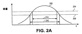
図2Aおよび図2Bは、露光または線量曲線に相対的に高いエッジ傾斜をもたらすようにレジスト上のパターンを露光することによってどのように限界寸法変動を低減できるかを示し、これは「荷電粒子ビームリソグラフィを用いて精度の高いパターンを形成するための方法およびシステム(Method and System for Forming High Accuracy Patterns Using Charged Particle Beam Lithography)」と題される、2012年4月19日に出願された米国特許公開第2012/0096412号などに記載されているものであり、これをすべての目的で引用によりここに援用する。図2Aは断面線量曲線202を示し、x軸はパターンの2つのエッジに垂直な距離といった、露光パターンを通る断面距離を示し、y軸はレジストが受けた線量を示す。受けた線量がしきい値よりも高いレジストによってあるパターンが描出される。2つのしきい値が図2Aに示され、レジスト感度の変動の影響を示す。より高いしきい値204では、幅214のパターンがレジストによって描出される。より低いしきい値206では、幅216のパターンがレジストによって描出され、幅216は幅214よりも大きい。図2Bは別の断面線量曲線222を示す。2つのしきい値が示され、しきい値224は図2Aのしきい値204と同じであり、しきい値226は図2Aのしきい値206と同じである。線量曲線222の傾斜は、線量曲線202の傾斜よりも、2つのしきい値の近くではより高い。線量曲線222において、より高いしきい値224では、幅234のパターンがレジストによって描出される。より低いしきい値226では、幅236のパターンがレジストによって描出される。見てわかるように、幅236と幅234との間の差は、線量曲線202と比べて線量曲線222のエッジ傾斜がより高いので、幅216と幅214との間の差よりも小さい。レジスト被覆表面がレチクルであるのなら、レジストしきい値の変動に対するより低い感度の曲線222により、レチクルから製造されたフォトマスク上のパターン幅は、フォトマスク用の目標パターン幅により近くなり、それによりフォトマスクを用いてパターンをシリコンウェハなどの基板に転写する場合に、使用可能な集積回路の歩留まりを上げる。各ショットの線量の変動に対する許容差の同様の向上も、より高いエッジ傾斜を有する線量曲線で見られる。したがって、線量曲線222のような相対的に高いエッジ傾斜を達成することが望ましい。
FIGS. 2A and 2B show how critical dimension variations can be reduced by exposing a pattern on the resist to provide a relatively high edge slope in the exposure or dose curve, which is described in “Charged Particle Beams”. US patent application filed April 19, 2012 entitled "Method and System for Forming High Accuracy Patterns Using Charged Particle Beam Lithography" No. 2012/0096412, etc., which is incorporated herein by reference for all purposes. FIG. 2A shows a
上記のように、処理の変動はフォトマスク上のパターンの幅が意図されるまたは目標の幅と異なることを引起し得る。フォトマスク上のパターン幅の変動は、光学リソグラフィプロセスでフォトマスクを用いて露光されたウェハ上にパターン幅の変動を引起す。フォトマスクパターン幅の変動に対するウェハパターン幅の感度は、マスクエッジ誤差係数、すなわちMEEFと呼ばれる。4×のフォトマスクを用いた光学リソグラフィシステムであって、光学リソグラフィプロセスにおいてフォトマスクパターンの4分の1の縮小版をウェハに投影するシステムでは、たとえば1のMEEFとは、フォトマスク上のパターン幅に1nmの誤差があれば、ウェハ上のパターン幅は0.25nm変わることを意味する。2のMEEFとは、フォトマスクパターン幅の1nmの誤差に対して、ウェハ上のパターン幅は0.5nm変わることを意味する。最も小さい集積回路の処理では、MEEFは2よりも大きくあり得る。 As noted above, process variations can cause the pattern width on the photomask to differ from the intended or target width. Variations in the pattern width on the photomask cause variations in the pattern width on the wafer exposed using the photomask in the optical lithography process. The sensitivity of the wafer pattern width to variations in the photomask pattern width is called the mask edge error coefficient, or MEEF. In an optical lithography system using a 4 × photomask, in which a reduced version of a photomask pattern is projected onto a wafer in an optical lithography process, for example, one MEEF is a pattern on the photomask. If there is an error of 1 nm in the width, it means that the pattern width on the wafer changes by 0.25 nm. The MEEF of 2 means that the pattern width on the wafer changes by 0.5 nm with respect to an error of 1 nm in the photomask pattern width. For the processing of the smallest integrated circuits, the MEEF can be greater than 2.
図3Aは、斜めの経路または軌道を形成する従来の非重畳VSBショットの組300の例を示す。ショットの組300は、ショット302、ショット304、ショット306、ショット308、ショット310、ショット312、ショット314、ショット316、ショット318およびショット320からなる。ショットは、付近のショットと当接するが、重ならない。図3Bは、ショットの組300が表面において形成してもよいパターン352を示す。パターン352は太い破線として示される。荷電粒子ビームシミュレーションを用いてショットの組300から経路352を計算してもよい。理解することが可能であるように、パターン352は、角丸み付けを示す。パターン352のCDは、その垂直の幅であり、それは経路の最長寸法と垂直な方向における寸法である。一般に測定されるように、パターン352のような変動する幅パターンのCDは、その平均寸法354であると考慮される。理解することが可能であるように、経路352の垂直の幅は、単一のショットによってはどこにも判断されない。たとえば、線330に沿って、ショット306および308はCDを決定し、それによって、線330に沿って分割されたCDを形成する。したがって、経路352はその全長に沿って分割されたCDの影響の対象である。
FIG. 3A shows an example of a conventional non-overlapping VSB shot set 300 that forms a diagonal path or trajectory. The shot set 300 includes a
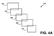
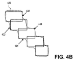
図4Aは、本開示の別の実施の形態に従って、表面において線形の非マンハッタン軌道を形成する5つの重畳VSBショットからなる組ショット400の例を示す。ショットの組400は、ショット402、ショット404、ショット406、ショット408およびショット410からなる。軌道における内部のショット−ショット404、406および408−に関して、最も近い近隣のショットのx−オフセットおよびy−オフセットは一様であり、近隣のショット間において一様な重畳を形成する。図4Bは、図4Aのショットの組を、ショットの組400がレチクルのような表面上に形成する、破線で示されたパターン420とともに示す。パターン420の限界寸法432は、あるCD分割を有し、なぜならば、限界寸法432は2つのショットによって形成されるからである。限界寸法434はCD分割を有さず、なぜならば、限界寸法434は1つのショットのみによって形成されるからである。重畳ショットで、ショットサイズおよび重畳の量を変動させて、異なる量のCD分割を達成することが可能である。
FIG. 4A shows an example of a
図5A〜5Dは、さまざまなショットサイズおよび重畳がレチクルのような表面において異なるパターン特性を生じさせる線形非マンハッタン軌道を形成することが可能であるショットの4つの例を示す。図5A〜5Dでは、軌道の縁部は、軌道の長さの大部分に関しておおよそ平行である。軌道は少なくとも1つの幅および角度によって記述されてもよい。図5Aはショットの組510を示す。線分512は、ショットの組510によって形成される軌道の方向と垂直であり、軌道の頂部上の「ピーク」は軌道の底部上の「谷」と対応することを示すよう位置決めされる。この構成は、最小の線幅粗さ(LWR)で軌道を形成することが可能であるが、しかし、それは中程度のCD分割を有する。図5Bは、別のショットの組520を示す。線分522は、ショットの組520によって形成される軌道の方向と垂直であり、軌道の対向する縁部は単一のショットから形成され、最小のCD分割を生じさせることを示すよう位置決めされる。しかしながら、ショット520の組は、線分522のようなピークからピークへの位置決めおよび谷から谷への位置決めと対応する線幅のため、最大LWRを生じさせる。図5Cは、別のショットの組530を示す。線分532はショットの組530によって形成される軌道の方向と垂直である。線分532は、ショットの組530によって形成される軌道の上側縁部上の谷に位置決めされるが、軌道の底縁部上のピーク近くにある。ショットの組530は低いLWRを生じさせるが、中程度のCD分割を生じさせる。図5Dは、別のショットの組540を示す。線分542はショットの組540によって形成される軌道の方向と垂直である。ショットの組540のショットサイズおよびショット重畳は、最大のCD分割を生じさせ、ショットの組によって形成された軌道の至る所にCD分割がある。ショットの組540は中程度のLWRを生じさせる。
FIGS. 5A-5D show four examples of shots where various shot sizes and overlays can form linear non-Manhattan trajectories that produce different pattern characteristics on a reticle-like surface. In FIGS. 5A-5D, the edges of the track are approximately parallel for most of the length of the track. A trajectory may be described by at least one width and angle. FIG. 5A shows a
レチクル上に形成されるパターンのCDUは、荷電粒子ビームリソグラフィプロセスにおいて内在的なランダムな変動および体系的な変動を明らかにすることによって、より正確にモデル化されてもよい。1つの実施の形態では、モンテカルロ法を用いてこれらの変動を明らかにしてもよい。このように、線形軌道のようなパターンのCDUは、モンテカルロ解析を用いて確率論的に計算されてもよい。軌道のCDUは複数の独自のモンテカルロシミュレーションに基いて判断されてもよく、各シミュレーションごとに、軌道を含む各ショットは、1つ以上の製造パラメータにおいて変動を受ける。各独自のモンテカルロシミュレーションごとに、変動されたショットの組からのレチクル像が計算される。各計算されたレチクル像ごとに、パターンCDが測定される。その測定は、レチクル上の製造されたパターンの物理的な走査電子顕微鏡(SEM)測定を行なうのに一般に用いられる技術と同様の技術が用いられてもよい。各シミュレーションが測定されたCDを有する、複数の独自のモンテカルロシミュレーションからの結果として生じる測定値の集団は、CD分布を含む。VSB、CPまたは組み合わせたVSBおよびCPショットの群が、このように解析されてもよい。 The CDU of the pattern formed on the reticle may be more accurately modeled by revealing inherent random and systematic variations in the charged particle beam lithography process. In one embodiment, these variations may be accounted for using the Monte Carlo method. Thus, a CDU having a pattern such as a linear trajectory may be calculated stochastically using Monte Carlo analysis. The trajectory CDU may be determined based on a plurality of unique Monte Carlo simulations, and for each simulation, each shot including the trajectory is subject to variations in one or more manufacturing parameters. For each unique Monte Carlo simulation, a reticle image from a varied set of shots is calculated. A pattern CD is measured for each calculated reticle image. The measurement may use techniques similar to those commonly used to perform physical scanning electron microscope (SEM) measurements of the manufactured pattern on the reticle. The resulting population of measurements from a plurality of unique Monte Carlo simulations, each simulation having a measured CD, includes a CD distribution. A group of VSB, CP or combined VSB and CP shots may be analyzed in this way.
図6は、軌道を形成するよう用いられてもよいさまざまなショット構成を用いて、CD分布グラフ600の例を示す。この例では、軌道は、軌道が100nmの公称のデザイン幅を有する、非マンハッタン線形軌道である。3つのショット構成が解析された:
・曲線610:軌道の角度および100nmの幅に基づく従来的に計算されたショット寸法を用いる、従来の非重畳VSBショット。
・曲線612:重畳VSBショット。ある重畳VSBショットの構成が、モデルに基づく技術を用いて決定され、このショット構成は100nmの軌道を形成することが可能であり、ショットからショットへの間隔およびしたがってショット数は上記の従来の非重畳ショット構成と同じである。
・曲線614:重畳円形キャラクタ投影ショット。100nmの軌道を形成することが可能であり、ショットからショットへの間隔およびしたがってショット数が上記の従来の非重畳ショット構成と同じである、円形のショット構成が決定された。
この実験では、3つのショット構成はすべて、製造ばらつきの影響が加えられる前に、同じ事前PEC線量を用いた。他の実施の形態では、異なる割当てられた線量でのショットが、結果としての線量マージン変動とともに、さらに可能である。加えて、他の実施の形態では、スライバ低減を変動させてもよい。次いで、モンテカルロ技法を用いて、CDUに対する製造ばらつきの影響が、各ショット構成を用いて形成された軌道に対して計算された。2つのパラメータが変更された:
・ショット線量は、通常の線量の5%のシグマで、正規分布を用いて変更された。
・各ショットの位置は、1.5nmのシグマで、正規分布を用いて変更された。CD分割が存在するショット構成に関して、変動するショット位置は、CD分割の影響をモデル化する。
いくつかの実施の形態では、図6の実験ではそうではなかったが、ショットサイズを変更することも考えられる。サイズ変動は、幅、高さ、または幅および高さ共、のような要素を含み得る。図6は、グラフ600においてこの実験の結果を示し、曲線610、612および614に関して上に挙げられたショット構成を用いて形成された線形非マンハッタン軌道に対するCDの確率分布を示す。グラフ600のX軸はCDであり、100.0nmはデザイン幅である。グラフ600のy軸は条件付確率である。すべてのCD確率の和が1であるので、3つの曲線の各々の下の領域は等しい。各CD曲線の1−シグマは次のとおりである:
・曲線610:0.49nm
・曲線612:0.33nm
・曲線614:0.32nm
加えて、さまざまなショット構成のLWRは次のとおりである:
・従来の非重畳ショット(曲線610):4.13nm
・最適化された重畳VSBショット(曲線612):2.83nm
・最適化された重畳円形CPショット(曲線614):2.70nm
この例における重畳ショットの使用は、従来のショットと比較して、CDUおよびLWRが両方とも改善され得ることを示す。さらに、円形のCPショットの使用はVSBショットの使用より多くの改善を与え得る。同じショットからショットへの間隔を用いる重畳VSBショットの他の組は、CD分布612よりさらによいCDUを示し得る。同様に、同じショットからショットへの間隔を用いるCPショットの他の組は、CD分布614よりさらによいCDUを示し得る。
FIG. 6 shows an example of a
Curve 610: a conventional non-overlapping VSB shot using a conventionally calculated shot size based on the trajectory angle and 100 nm width.
Curve 612: superimposed VSB shot. The configuration of a superimposed VSB shot is determined using a model-based technique, which can form a 100 nm trajectory, and the shot-to-shot spacing and hence the number of shots is This is the same as the superimposed shot configuration.
Curve 614: Superposed circular character projection shot. A circular shot configuration was determined in which 100 nm trajectories can be formed and the shot-to-shot spacing and thus the number of shots is the same as the conventional non-overlapping shot configuration described above.
In this experiment, all three shot configurations used the same pre-PEC dose before the effects of manufacturing variability were added. In other embodiments, shots with different assigned doses are further possible, with resulting dose margin variations. In addition, in other embodiments, sliver reduction may be varied. Then, using Monte Carlo techniques, the effect of manufacturing variability on the CDU was calculated for the trajectory formed using each shot configuration. Two parameters have been changed:
The shot dose was sigma 5% of the normal dose and was modified using a normal distribution.
The position of each shot was 1.5 nm sigma and changed using a normal distribution. For shot configurations where there is CD splitting, the changing shot position models the effect of CD splitting.
In some embodiments, it may be possible to change the shot size, although this was not the case in the experiment of FIG. The size variation may include elements such as width, height, or both width and height. FIG. 6 shows the results of this experiment in
Curve 610: 0.49 nm
Curve 612: 0.33 nm
Curve 614: 0.32 nm
In addition, the LWRs for the various shot configurations are as follows:
Conventional non-overlapping shot (curve 610): 4.13 nm
Optimized superimposed VSB shot (curve 612): 2.83 nm
Optimized overlapped circular CP shot (curve 614): 2.70 nm
The use of superimposed shots in this example shows that both CDU and LWR can be improved compared to conventional shots. Furthermore, the use of circular CP shots can provide more improvements than the use of VSB shots. Other sets of superimposed VSB shots using the same shot-to-shot spacing may show a better CDU than
同様の技術を用いて、曲線から成る軌道のCDUを計算し、より一般的なレチクルパターンの寸法の可変性を計算してもよい。用語「限界寸法」は一般に軌道にのみ適用されるが、同様の用語「ウェハ限界寸法」は物理的デザインにおいて任意のパターンの所望の寸法を指す。CDUの最適化に関して述べられた技術は、ウェハ限界寸法均一性を最適化するように用いることも可能である。 Similar techniques may be used to calculate the CDU of the trajectory consisting of curves and to calculate the variability of the dimensions of the more general reticle pattern. The term “critical dimension” generally applies only to the trajectory, but the similar term “wafer critical dimension” refers to the desired dimension of any pattern in the physical design. The techniques described for CDU optimization can also be used to optimize wafer critical dimension uniformity.
図6の実験では、ショットからショットへの間隔は、さまざまなショット構成において一定である。一般には、しかしながら、ショットからショットへの間隔は、変動してもよい。たとえば、ショットからショットへの間隔が増大される場合、ショットの数は減少し、したがって、レチクル上にパターンを書込むのに必要な時間は減少する。図7は、従来のショットの組および重畳ショットの2つの構成に対するCD分布を示す:
・曲線710は、従来の非重畳VSBショットの組に対するCD分布を示す。6シグマCDUは4.8nmである。
・曲線712は、重畳VSBショットのCDU最適化された組に対するCD分布を示し、書込時間は従来の非重畳ショットに対してと同じである。6シグマCDUは3.2nmである。
・曲線714は、重畳VSBショットのCDU最適化された組に対するCD分布を示し、書込時間は、従来の非重畳ショットに対する書込時間の70%である。6シグマCDUは4.8nmである。
図6の実験におけるように、ショット線量およびショット位置における製造ばらつきが、この実験において計算された。この実験では、3つのショット構成はすべて、製造ばらつきの影響が加えられる前に、同じ事前PEC線量を用いた。他の実施の形態では、異なる割当てられた線量でのショットが、結果としての線量マージン変動とともに、さらに可能である。図7で示されたCDU分布は、重畳ショットを用いることによって可能にされる柔軟性によって、書込時間を維持しながら、CDUが従来の非重畳ショットよりも改善されるのを可能にするか、または、CDUを維持しながら書込時間が低減されることを可能にすることを示す。他の解決策は、これらの2つの解決策の間に見出されてもよく、CDUおよび書込時間が同時に改善される。
In the experiment of FIG. 6, the shot-to-shot spacing is constant for various shot configurations. In general, however, the shot-to-shot interval may vary. For example, if the shot-to-shot interval is increased, the number of shots decreases, and therefore the time required to write the pattern on the reticle decreases. FIG. 7 shows the CD distribution for two configurations of conventional shot sets and superimposed shots:
Curve 710 shows the CD distribution for a set of conventional non-overlapping VSB shots. The 6 sigma CDU is 4.8 nm.
As in the experiment of FIG. 6, the shot dose and manufacturing variability at the shot position were calculated in this experiment. In this experiment, all three shot configurations used the same pre-PEC dose before the effects of manufacturing variability were added. In other embodiments, shots with different assigned doses are further possible, with resulting dose margin variations. Does the CDU distribution shown in FIG. 7 allow the CDU to be improved over conventional non-overlapping shots while maintaining writing time, with the flexibility enabled by using overlapping shots? Or it shows that the write time can be reduced while maintaining the CDU. Other solutions may be found between these two solutions, improving CDU and write time simultaneously.
上記の実験では、独自のモンテカルロシミュレーションにおけるショットの各組ごとに、レチクル像が、荷電粒子ビームシミュレーションを用いて計算されてもよい。荷電粒子ビームシミュレーションによって用いられるマスクモデルに含まれ得る影響は、前方散乱、後方散乱、レジスト拡散、クーロン効果、エッチングおよびフォギング、ローディング、レジスト帯電を含む。 In the above experiment, a reticle image may be calculated for each set of shots in a unique Monte Carlo simulation using a charged particle beam simulation. Effects that may be included in the mask model used by the charged particle beam simulation include forward scatter, back scatter, resist diffusion, Coulomb effect, etching and fogging, loading, resist charging.
上記の実験では、レチクルまたはフォトマスク上のCD分布が計算された。他の実施の形態では、ダブルシミュレーションが用いられてもよく、基板空間像が、シミュレーションされたレチクル像を用いた光学リソグラフィプロセスを用いて計算される。リソグラフィシミュレーションを用いて基板空間像を計算してもよい。ダブルシミュレーションは、この開示の関連出願セクションにおいてリスト化された米国特許出願に開示される。 In the above experiment, the CD distribution on the reticle or photomask was calculated. In other embodiments, double simulation may be used, and the substrate aerial image is calculated using an optical lithography process with a simulated reticle image. A substrate aerial image may be calculated using lithography simulation. Double simulations are disclosed in the US patent applications listed in the related applications section of this disclosure.
図8は、シリコンウェハのような基板上に、本開示の別の実施の形態に従って、光学リソグラフィを用いて、パターンを形成するための概念的フロー図800である。第1のステップ802において、物理的デザイン、たとえば集積回路の物理的デザインが設計される。これは論理ゲート、トランジスタ、金属層、および物理的デザインにあるべき他の項目、たとえば集積回路の物理的デザインなどを含み得る。次に、ステップ804で、OPCが、物理的デザイン802におけるパターン上、または物理的デザインにおけるパターンの一部上で行なわれて、マスクデザイン806を形成する。OPCステップ804は、リソグラフィおよび基板処理効果を組込むが、荷電粒子ビーム露光およびレチクル処理効果は組込まない基板モデル840を用いる。基板処理効果は、たとえば、基板レジストベークおよび基板レジスト現像を含んでもよい。いくつかの実施の形態では、OPCはインバースリソグラフィ技術(ILT)を含んでもよい。ステップ808で、マスクデザイン806は、荷電粒子ビームショットの組、ショットリスト810にフラクチャリングされる。ショットは重畳してもよい。いくつかの実施の形態では、ショットはVSBショットになる。他の実施の形態では、ショットはCPショットまたはVSBショットとCPショットとの組合せになる。マスクデータ準備(MDP)最適化808は、1つ以上の潜在的なショット構成に関してCDUを計算することを含んでもよく、1つ以上の製造パラメータを変動させることによってCD分布を計算することを含んでもよい。1つの実施の形態では、モンテカルロ解析を用いてCD分布を計算してもよい。MDP808は、さらに、入力としてマスクモデル842を用いる。マスクモデル842に含まれてもよい物理的現象は、前方散乱、後方散乱、クーロン効果、フォギング、レジスト帯電、ローディング、レジストベーク、レジスト現像、およびレジストエッチングを含む。いくつかの実施の形態では、MDP808は、基板モデル840を用いて、基板上で空間像を計算するために、リソグラフィシミュレーションを用いてもよい。基板モデル840は、光学リソグラフィ効果を含んでもよく、さらに、レジストベークおよびレジスト現像のようなレジスト効果を含んでもよい。MDP808はマスク像826上のCDUの最適化を含んでもよく、および/または基板上の空間像CDUの最適化を含んでもよい。MDP808は、ショット構成ライブラリ844から予め演算されたショットの組を入力してもよい。ショット構成ライブラリ844は、所与のパターン形状および構成に対して使用するショットアスペクト比を指定する参照テーブルを含んでもよい。MDP808はマスクプロセス補正(MPC)を含んでもよい。MDP808はショットリスト810を出力する。
FIG. 8 is a conceptual flow diagram 800 for forming a pattern on a substrate, such as a silicon wafer, using optical lithography, according to another embodiment of the present disclosure. In a
近接効果補正(PEC)改善ステップ820において、ショットリスト810におけるショットのショット線量は、長距離効果を明らかにするよう調整されるが、それは、後方散乱、ローディング、フォギング、およびレジスト帯電を含んでもよい。PEC改善820の出力は調整された線量を伴う最終ショットリスト822である。調整された線量を伴う最終ショットリスト822はマスク書込ステップ824において表面を生成するために用いられるが、これは電子ビームライタシステムなどの荷電粒子ビームライタを用いる。用いられている荷電粒子ビームライタのタイプによっては、PEC改善820は荷電粒子ビームライタによって実行されてもよい。マスク書込ステップ824は、単一露光パスまたは複数露光パスを含んでもよい。電子ビームライタシステムは、レジストでコーティングされた表面上に電子ビームを投射して、ステップ826において示されるように、表面上にパターンを含むマスク像を形成する。付加的処理ステップ(図示せず)の後に、次いで、完成した表面は、ステップ828において示される光学リソグラフィ装置において用いられて、シリコンウェハのようなレジストでコーティングされた基板を露光して、レジスト上に潜像830を形成してもよい。次いで、露光された基板は、レジストベークおよびレジスト現像のようなさらなるレジスト処理ステップ832を経て、基板上にパターン834を形成する。
In proximity effect correction (PEC)
図9は、先在するショットリストの最適化のための概念的フロー図900である。フロー900は、所望のレチクルパターン902および予備的ショットリスト904で始まり、予備的ショットリスト904は所望のレチクルパターン902をおおよそ形成することが可能である。MDPステップ910は予備的ショットリスト904においてショットを修正して、所望のレチクルパターン902を予備的ショットリスト904より正確に形成することが可能である、結果として生じる最適化されたショットリスト912を形成する。最適化されたショットリスト912におけるショットは、重畳してもよく、異なる割当てられた線量を有してもよい。MDP/ショット最適化910は、1つ以上の潜在的なショット構成に関してCDUを計算することを含んでもよく、1つ以上の製造パラメータを変動させることによってCD分布を計算することを含んでもよい。1つの実施の形態では、モンテカルロ解析を用いてCD分布を計算してもよい。MDP/ショット最適化910は、さらに、最終のマスクモデル906を入力として用いる。最終のマスクモデル906に含まれてもよい物理的現象は、前方散乱、後方散乱、クーロン効果、フォギング、レジスト帯電、ローディング、レジストベーク、レジスト現像、およびレジストエッチングを含む。いくつかの実施の形態では、MDP/ショット最適化910は、基板モデル908を用いて、基板上で空間像を計算するために、リソグラフィシミュレーションを用いてもよい。基板モデル908は、光学リソグラフィ効果を含んでもよく、さらに、レジストベークおよびレジスト現像のようなレジスト効果を含んでもよい。CD分布がいつ計算されるかのようないくつかの実施の形態において、荷電粒子ビームおよび/またはリソグラフィシミュレーションを、製造ばらつきを表すような複数の条件に対して実行してもよい。これらの実施の形態の1つでは、最適化は製造ばらつきの影響を組込む評点を計算することを含んでもよい。MDP/ショット最適化910はマスク像920上のCDUの最適化を含んでもよく、および/または基板上の空間像CDUの最適化を含んでもよい。MDP910はさらにマスクプロセス補正(MPC)を含んでもよい。近接効果補正(PEC)改善ステップ914において、最適化されたショットリスト912におけるショットのショット線量は、長距離効果を明らかにするよう調整されるが、それは、後方散乱、ローディング、フォギング、およびレジスト帯電を含んでもよい。PEC改善914の出力は、最終ショットリスト916である。最終ショットリスト916はマスク書込ステップ918において表面を生成するために用いられるが、これは電子ビームライタシステムなどの荷電粒子ビームライタを用いる。用いられている荷電粒子ビームライタのタイプによっては、PEC改善914は荷電粒子ビームライタによって実行されてもよい。マスク書込ステップ918は、単一露光パスまたは複数露光パスを含んでもよい。電子ビームライタシステムは、ステンシルを介して表面上に電子ビームを投射して、ステップ920において示されるように、表面上にパターンを含むマスク像を形成する。さらなる処理ステップ(図示せず)の後に、次いで、完成した表面は、ステップ922において示される光学リソグラフィ装置において用いられて、シリコンウェハのようなレジストでコーティングされた基板を露光して、レジスト上に潜像924を形成してもよい。次いで、露光された基板は、レジストベークおよびレジスト現像のようなさらなるレジスト処理ステップ926を経て、基板上にパターン928を形成する。
FIG. 9 is a conceptual flow diagram 900 for optimization of a pre-existing shot list. The
フロー900は、たとえば、予備的ショットリスト904が形成されてから、レチクル処理ステップが変化して、マスクモデル変更を引起し、それが予備的ショットリスト904においてショットの再最適化を必要とするときに、有用であってもよい。
The
既存のショットリストを検証して、CDUが期待される製造ばらつきに照らして予め定められた許容差内にあるかどうかを判断してもよい。図10は、この技術の1つの実施の形態の概念的フロー図1000である。プロセスに対する入力は既存のショットリスト1004である。ショット検証ステップ1010においては、レチクルパターンが複数のショットリスト変動の各々に関して計算され、各ショットリスト変動におけるショットは製造ばらつきの影響を組込み、各レチクルパターンの計算も、製造ばらつきの影響を組込む。したがって、各計算されたレチクルパターンは異なるレチクル製造条件を表す。ステップ1010のレチクルパターン計算はマスクモデル1006を入力として用いる。CDが、各計算されたレチクルパターンごとに、1つ以上の位置で測定される。CDUが、複数の計算されたレチクルパターンの各々からのCDを用いて、各位置ごとに計算される。予め定められた許容差より大きいCDUは適合せず、例外レポート1012に出力される。いくつかの実施の形態では、ショット検証1010はダブルシミュレーションを含んでもよく、ウェハのような基板上の空間像が、リソグラフィシミュレーションを用いるなどして、各レチクルパターンごとに計算される。この場合、基板モデル1008もショット検証1010に入力される。ダブルシミュレーションを用いるこれらの実施の形態では、CDは各空間像の各測定位置で測定され、基板CDUは各測定位置ごとに各ショットリスト変動の空間像CDから計算される。
An existing shot list may be verified to determine if the CDU is within a predetermined tolerance in light of expected manufacturing variability. FIG. 10 is a conceptual flow diagram 1000 of one embodiment of this technique. The input to the process is an existing
所与の情況に対して最小のCDUを生じさせるショット構成が予め計算されてもよく、このショット構成についての情報はテーブルに保存されてもよい。たとえば、ある情況は、X軸から40度の角度を付けられた、100nmの幅を伴う線形軌道であってもよく、それに対してショット構成が予め計算されることになる。軌道それ自体に加えて、情況は近くの環境を含んでもよい。この例では、環境はショットが生成されることになっている軌道の各側に複数の少なくとも5つの平行な100nm幅の軌道含み、隣接する軌道は100nmの空間によって分離されてもよい。所与の情況のための最善のショット構成を判断する際に、他のパラメータも考慮されてもよい。たとえば、ショット構成をレチクル上に露光し、レチクルを処理してフォトマスクを形成し、製造されたフォトマスクパターン寸法を測定し、これらの測定された寸法を計算されたパターン寸法と比較してもよく、計算および測定された寸法間の平均差は平均値対目標値(MTT)である。予め定められる値より下にMTTを有するショット構成のみがテーブルに保存されてもよい。 A shot configuration that produces the smallest CDU for a given situation may be pre-calculated and information about this shot configuration may be stored in a table. For example, one situation may be a linear trajectory with a width of 100 nm, angled 40 degrees from the X axis, for which the shot configuration will be pre-calculated. In addition to the orbit itself, the situation may include a nearby environment. In this example, the environment includes a plurality of at least five parallel 100 nm wide trajectories on each side of the trajectory from which shots are to be generated, and adjacent trajectories may be separated by a 100 nm space. Other parameters may also be considered in determining the best shot configuration for a given situation. For example, even if the shot configuration is exposed on a reticle, the reticle is processed to form a photomask, the manufactured photomask pattern dimensions are measured, and these measured dimensions are compared to the calculated pattern dimensions. Often, the average difference between the calculated and measured dimensions is the average value versus the target value (MTT). Only shot configurations having MTT below a predetermined value may be stored in the table.
この開示において記載または言及される計算は、さまざまな態様で達成されてもよい。一般的に、計算は処理内方法、前処理方法、または後処理方法によって達成されてもよい。処理内計算は、その結果が必要なときに計算を行なうことを含む。前処理計算は、予め計算し、その結果を記憶して、後の処理工程で検索することを含み、特に何回も繰返される計算では、処理性能を向上させ得る。計算は、ある処理工程で延期させて、後の後処理工程で行なうこともできる。前処理計算の一例は、所与の情況に対して最小のCDUを生じさせるショット構成を予め計算すること、およびこのショット構成についての情報をテーブルに保存することである。前処理計算の別の一例はショットグループであり、これは所与の入力パターンまたは入力パターン特性の組に関連付けられる1つ以上のショットについての線量パターン情報の事前計算である。ショットグループおよび関連付けられている入力パターンは、事前計算ショットグループのライブラリ内に保存することができ、ショットグループをなすショットの組は、パターンを再度計算することなく、入力パターンの付加的インスタンスのために迅速に生成することができる。一部の実施の形態において、事前計算は、ショットグループがレジスト被覆表面にもたらす線量パターンのシミュレーションを含み得る。他の実施の形態において、ショットグループは、たとえばコレクトバイコンストラクション(correct-by-construction)技術を用いることによるなどして、シミュレーションを用いずに定めることができる。一部の実施の形態において、事前に計算されたショットグループは、ショットリストの形で、ショットグループライブラリ内に保存することができる。他の実施の形態において、事前計算されたショットグループは、コンピュータコードの形で保存することができ、これは特定の種類の入力パターン向けのショットを生成することができる。さらに他の実施の形態において、複数の事前計算されたショットグループはテーブルの形で保存することができ、表の入力はパターン幅といったさまざまな入力パターンまたは入力パターン特性に対応し、各テーブル入力は、ショットグループのショットのリスト、または適切なショットの組をどのように生成するかについての情報を提供する。さらに、異なるショットグループは、ショットグループライブラリにおいて異なる形で保存することもできる。一部の実施の形態において、所与のショットグループが作成できる線量パターンも、ショットグループライブラリに保存することができる。一実施の形態において、線量パターンは、グリフと呼ばれる二次元(XおよびY)線量マップとして保存することができる。 The calculations described or referred to in this disclosure may be accomplished in various ways. In general, the computation may be accomplished by an in-process method, a pre-processing method, or a post-processing method. In-process calculations include performing calculations when the results are needed. Pre-processing calculations include pre-calculating, storing the results, and retrieving in subsequent processing steps, especially in calculations that are repeated many times, and can improve processing performance. The calculation can also be postponed in one processing step and performed in a later post-processing step. An example of a pre-processing calculation is to pre-calculate a shot configuration that yields the smallest CDU for a given situation and store information about this shot configuration in a table. Another example of a pre-processing calculation is a shot group, which is a pre-calculation of dose pattern information for one or more shots associated with a given input pattern or set of input pattern characteristics. Shot groups and associated input patterns can be stored in a library of pre-computed shot groups, and the set of shots that make up a shot group can be used for additional instances of the input pattern without recomputing the pattern. Can be generated quickly. In some embodiments, the pre-computation may include a simulation of the dose pattern that the shot group brings to the resist coated surface. In other embodiments, shot groups can be defined without simulation, such as by using a correct-by-construction technique. In some embodiments, pre-computed shot groups can be stored in a shot group library in the form of a shot list. In other embodiments, pre-computed shot groups can be stored in the form of computer code, which can generate shots for a particular type of input pattern. In still other embodiments, multiple pre-computed shot groups can be stored in the form of a table, the table entries corresponding to various input patterns or input pattern characteristics such as pattern width, and each table entry is Provide information about how to generate a list of shots in a shot group, or an appropriate set of shots. Further, different shot groups can be stored differently in the shot group library. In some embodiments, the dose patterns that a given shot group can create can also be stored in the shot group library. In one embodiment, the dose pattern can be saved as a two-dimensional (X and Y) dose map called a glyph.
本開示に記載されるフラクチャリング、マスクデータ準備、ショット最適化、および検証フローは、演算装置として適切なコンピュータソフトウェアを有する汎用コンピュータを用いて実施することができる。必要な大量の計算により、複数のコンピュータまたはプロセッサコアを並列に用いることができる。一実施の形態において、演算は並列処理をサポートするために、フローにおいて1つ以上の演算が多いステップに対して複数の二次元ジオメトリ領域にさらに分けることができる。別の実施の形態において、専用ハードウェア装置を単独で、または複数で用いて、汎用コンピュータまたはプロセッサコアを用いるよりも速い速度で1つ以上のステップの演算を行なうことができる。一実施の形態において、専用ハードウェア装置はグラフィックス処理ユニット(GPU)であり得る。別の実施の形態において、本開示に記載される最適化およびシミュレーション処理は、全体のショット数、または全体の荷電粒子ビーム書込時間、または他の何らかのパラメータを最小にするために、可能な解決策を修正および再計算する反復処理を含むことができる。さらに他の実施の形態において、最初のショットの組は、コレクトバイコンストラクション方法によって判断することができるので、ショット修正は必要ない。 The fracturing, mask data preparation, shot optimization, and verification flows described in this disclosure can be performed using a general purpose computer having suitable computer software as a computing device. Multiple computers or processor cores can be used in parallel due to the large amount of computation required. In one embodiment, the operations can be further divided into a plurality of two-dimensional geometry regions for steps with one or more operations in the flow to support parallel processing. In another embodiment, one or more dedicated hardware devices may be used to perform one or more steps of operation at a faster rate than using a general purpose computer or processor core. In one embodiment, the dedicated hardware device may be a graphics processing unit (GPU). In another embodiment, the optimization and simulation process described in this disclosure may be a possible solution to minimize overall shot count, or overall charged particle beam writing time, or some other parameter. Iterative processing to modify and recalculate strategies can be included. In yet another embodiment, the first shot set can be determined by a collect-by-construction method, so shot correction is not necessary.
本明細書は特定の実施の形態について詳細に説明されたが、当業者なら、上記を理解した上で、これらの実施の形態に対する変更、変形、または均等物を容易に考え付くこともできるであろう。フラクチャリング、マスクデータ準備、近接効果補正および光学近接補正のための本方法に対する上記、または他の変形および変更は、特許請求の範囲により特定的に記載されている本主題の精神および範囲から逸脱することなく、当業者によって実現され得る。さらに、当業者なら、上記は一例であって、限定されるべきことが意図されていないものであると理解するであろう。ステップは、本発明の範囲から逸脱することなく、本明細書のステップに加える、取除く、または変えることができる。一般に、提示されているフローチャートはある機能を達成するために基本的動作の1つの可能なシーケンスを示すよう意図されるにすぎず、多くの変更が可能である。したがって、本主題は添付の特許請求の範囲およびその均等物の範囲内に入る変形および修正を網羅することが意図される。 Although the present specification has been described in detail for particular embodiments, those skilled in the art can readily devise changes, modifications, or equivalents to these embodiments with an understanding of the above. Let's go. These and other variations and modifications to the present method for fracturing, mask data preparation, proximity effect correction and optical proximity correction depart from the spirit and scope of the present subject matter as specifically described by the claims. Without, it can be realized by those skilled in the art. Further, those skilled in the art will appreciate that the above is an example and is not intended to be limiting. Steps may be added, removed or changed to the steps herein without departing from the scope of the invention. In general, the presented flowchart is only intended to illustrate one possible sequence of basic operations to accomplish a function, and many variations are possible. Accordingly, the subject matter is intended to embrace alterations and modifications that fall within the scope of the appended claims and their equivalents.
Claims (14)
荷電粒子ビームショットの組を決定するステップを含み、前記ショットの組は、荷電粒子ビームライタにおいて用いられたときに、レジストが被覆された表面に線量を生成し、前記レジストが被覆された表面の前記線量は、前記表面にパターンを形成し、製造ばらつきに起因する限界寸法均一性(CDU)が、ショット形状、一次元または二次元のショットサイズ、ショット位置、ショット間の間隔、ショット重なり、近接効果補正前のショット線量、線量マージン、限界寸法分割、スライバ低減、ショット数および書込時間からなる群から選択された要素を変化させた時に前記表面に生成されるであろうパターンを計算することによって最適化され、前記決定するステップは、コンピューティングハードウェア装置を用いて実行される、方法。 A method for mask data preparation (MDP) or mask process correction (MPC) for use with charged particle beam simulation comprising:
Determining a set of charged particle beam shots, the set of shots, when used in a charged particle beam writer, generating a dose on a resist coated surface, The dose forms a pattern on the surface, and critical dimension uniformity (CDU) due to manufacturing variation is shot shape, one-dimensional or two-dimensional shot size, shot position, distance between shots, shot overlap, proximity Calculating the pattern that will be generated on the surface when changing an element selected from the group consisting of shot dose before effect correction, dose margin, critical dimension division, sliver reduction, number of shots and writing time And the step of determining is performed using a computing hardware device. .
荷電粒子ビームショットの組を入力するステップと、
コンピューティングハードウェア装置を用いて、前記荷電粒子ビームショットの組から表面上のパターンを計算するステップと、
計算されたパターンについて、製造ばらつきによって起こされる限界寸法均一性(CDU)を計算するステップと、
荷電粒子ビームショットの組を変更して、ある位置に対するCDUを、その位置に対する前記CDUが予め定められたCDU許容量を上回る場合に、改善するステップとを含み、前記変更するステップは、i)ショット形状、ショットサイズ、ショット位置または近接効果補正前のショット線量を変更すること、またはii)ショットを加えることを含む、方法。 A method for mask data preparation (MDP) for use with charged particle beam lithography comprising:
Inputting a set of charged particle beam shots;
Calculating a pattern on a surface from the set of charged particle beam shots using a computing hardware device;
Calculating a critical dimension uniformity (CDU) caused by manufacturing variability for the calculated pattern;
Modifying the set of charged particle beam shots to improve the CDU for a location when the CDU for that location exceeds a predetermined CDU tolerance, the modifying step comprising: i) Changing the shot shape, shot size, shot position or shot dose before proximity effect correction, or ii) adding a shot.
Applications Claiming Priority (3)
| Application Number | Priority Date | Filing Date | Title |
|---|---|---|---|
| US201261625932P | 2012-04-18 | 2012-04-18 | |
| US61/625,932 | 2012-04-18 | ||
| PCT/US2013/036671 WO2013158574A1 (en) | 2012-04-18 | 2013-04-15 | Method and system for critical dimension uniformity using charged particle beam lithography |
Publications (3)
| Publication Number | Publication Date |
|---|---|
| JP2015515148A JP2015515148A (en) | 2015-05-21 |
| JP2015515148A5 JP2015515148A5 (en) | 2016-05-26 |
| JP6189933B2 true JP6189933B2 (en) | 2017-08-30 |
Family
ID=49381342
Family Applications (1)
| Application Number | Title | Priority Date | Filing Date |
|---|---|---|---|
| JP2015507093A Active JP6189933B2 (en) | 2012-04-18 | 2013-04-15 | Method and system for critical dimension uniformity using charged particle beam lithography |
Country Status (5)
| Country | Link |
|---|---|
| US (1) | US9038003B2 (en) |
| JP (1) | JP6189933B2 (en) |
| KR (1) | KR20150001834A (en) |
| TW (1) | TWI605302B (en) |
| WO (1) | WO2013158574A1 (en) |
Families Citing this family (31)
| Publication number | Priority date | Publication date | Assignee | Title |
|---|---|---|---|---|
| US9341936B2 (en) | 2008-09-01 | 2016-05-17 | D2S, Inc. | Method and system for forming a pattern on a reticle using charged particle beam lithography |
| US20120219886A1 (en) | 2011-02-28 | 2012-08-30 | D2S, Inc. | Method and system for forming patterns using charged particle beam lithography with variable pattern dosage |
| US9448473B2 (en) | 2009-08-26 | 2016-09-20 | D2S, Inc. | Method for fracturing and forming a pattern using shaped beam charged particle beam lithography |
| US9612530B2 (en) | 2011-02-28 | 2017-04-04 | D2S, Inc. | Method and system for design of enhanced edge slope patterns for charged particle beam lithography |
| US9034542B2 (en) | 2011-06-25 | 2015-05-19 | D2S, Inc. | Method and system for forming patterns with charged particle beam lithography |
| US9343267B2 (en) | 2012-04-18 | 2016-05-17 | D2S, Inc. | Method and system for dimensional uniformity using charged particle beam lithography |
| WO2013158573A1 (en) * | 2012-04-18 | 2013-10-24 | D2S, Inc. | Method and system for forming patterns using charged particle beam lithograph |
| US9299135B2 (en) * | 2013-03-12 | 2016-03-29 | Applied Materials Israel, Ltd. | Detection of weak points of a mask |
| JP6169876B2 (en) * | 2013-04-11 | 2017-07-26 | 日本コントロールシステム株式会社 | Electron beam drawing apparatus, drawing graphic data creation apparatus, electron beam drawing method, drawing graphic data creation method, and program |
| US9170501B2 (en) * | 2013-07-08 | 2015-10-27 | GlobalFoundries, Inc. | Methods for fabricating integrated circuits including generating photomasks for directed self-assembly |
| US9009634B2 (en) * | 2013-07-08 | 2015-04-14 | GlobalFoundries, Inc. | Methods for fabricating integrated circuits including generating photomasks for directed self-assembly |
| US9026956B1 (en) * | 2013-10-11 | 2015-05-05 | Taiwan Semiconductor Manufacturing Co., Ltd. | Method of lithographic process evaluation |
| US9023730B1 (en) | 2013-11-05 | 2015-05-05 | GlobalFoundries, Inc. | Methods for fabricating integrated circuits including generating e-beam patterns for directed self-assembly |
| CN105992975B (en) * | 2014-02-11 | 2018-06-01 | Asml荷兰有限公司 | For calculating the model changed at random of arbitrary graphic pattern |
| US9460260B2 (en) * | 2014-02-21 | 2016-10-04 | Mapper Lithography Ip B.V. | Enhanced stitching by overlap dose and feature reduction |
| KR102247563B1 (en) * | 2014-06-12 | 2021-05-03 | 삼성전자 주식회사 | Exposure method using E-beam, and method for fabricating mask and semiconductor device using the exposure method |
| US10074036B2 (en) * | 2014-10-21 | 2018-09-11 | Kla-Tencor Corporation | Critical dimension uniformity enhancement techniques and apparatus |
| EP3037878B1 (en) * | 2014-12-23 | 2020-09-09 | Aselta Nanographics | Method of applying vertex based corrections to a semiconductor design |
| US9747408B2 (en) * | 2015-08-21 | 2017-08-29 | Taiwan Semiconductor Manufacturing Company, Ltd. | Generating final mask pattern by performing inverse beam technology process |
| US9817927B2 (en) * | 2015-08-31 | 2017-11-14 | Globalfoundries Inc. | Hard mask etch and dielectric etch aware overlap for via and metal layers |
| EP3153926B1 (en) * | 2015-10-06 | 2020-04-22 | Aselta Nanographics | A method of reducing shot count in direct writing by a particle or photon beam |
| JP6515835B2 (en) * | 2016-02-23 | 2019-05-22 | 株式会社ニューフレアテクノロジー | Charged particle beam drawing apparatus and charged particle beam drawing method |
| US10466586B2 (en) | 2016-11-29 | 2019-11-05 | Taiwan Semiconductor Manufacturing Co., Ltd. | Method of modeling a mask having patterns with arbitrary angles |
| WO2019161899A1 (en) * | 2018-02-22 | 2019-08-29 | Applied Materials, Inc. | Method for automated critical dimension measurement on a substrate for display manufacturing, method of inspecting a large area substrate for display manufacturing, apparatus for inspecting a large area substrate for display manufacturing and method of operating thereof |
| US20200096876A1 (en) * | 2018-09-25 | 2020-03-26 | Asml Us, Llc F/K/A Asml Us, Inc. | Dose Map Optimization for Mask Making |
| DE102018217199A1 (en) * | 2018-10-09 | 2020-04-09 | Dr. Johannes Heidenhain Gmbh | Lattice structure for a diffractive optic |
| US10884395B2 (en) | 2018-12-22 | 2021-01-05 | D2S, Inc. | Method and system of reducing charged particle beam write time |
| US11604451B2 (en) | 2018-12-22 | 2023-03-14 | D2S, Inc. | Method and system of reducing charged particle beam write time |
| US11756765B2 (en) | 2019-05-24 | 2023-09-12 | D2S, Inc. | Method and system for determining a charged particle beam exposure for a local pattern density |
| US10748744B1 (en) | 2019-05-24 | 2020-08-18 | D2S, Inc. | Method and system for determining a charged particle beam exposure for a local pattern density |
| US20220128899A1 (en) * | 2020-10-22 | 2022-04-28 | D2S, Inc. | Methods and systems to determine shapes for semiconductor or flat panel display fabrication |
Family Cites Families (117)
| Publication number | Priority date | Publication date | Assignee | Title |
|---|---|---|---|---|
| JPS5425675A (en) | 1977-07-28 | 1979-02-26 | Nec Corp | Electron beam exposure unit |
| JPS608844A (en) | 1983-06-29 | 1985-01-17 | Pioneer Electronic Corp | Photoetching method with electron beams |
| JPS61105839A (en) | 1984-10-29 | 1986-05-23 | Toshiba Corp | Electron beam transferring mask and manufacture thereof |
| US4634871A (en) | 1985-01-14 | 1987-01-06 | Hughes Aircraft Company | Method and apparatus for spot shaping and blanking a focused beam |
| US4698509A (en) | 1985-02-14 | 1987-10-06 | Varian Associates, Inc. | High speed pattern generator for electron beam lithography |
| JPS637631A (en) | 1986-06-27 | 1988-01-13 | Omron Tateisi Electronics Co | Electron beam drawing |
| US4818885A (en) | 1987-06-30 | 1989-04-04 | International Business Machines Corporation | Electron beam writing method and system using large range deflection in combination with a continuously moving table |
| US5173582A (en) | 1988-10-31 | 1992-12-22 | Fujitsu Limited | Charged particle beam lithography system and method |
| JPH02280315A (en) | 1989-04-20 | 1990-11-16 | Mitsubishi Electric Corp | Electronic beam direct lithography device |
| JPH03205815A (en) | 1990-01-08 | 1991-09-09 | Hitachi Ltd | Variable fairing diaphragm |
| JPH04137520A (en) | 1990-09-28 | 1992-05-12 | Hitachi Ltd | Device and method for electron beam lithography |
| JPH04196516A (en) | 1990-11-28 | 1992-07-16 | Seiko Epson Corp | Ed exposing method and aligner |
| US5103101A (en) | 1991-03-04 | 1992-04-07 | Etec Systems, Inc. | Multiphase printing for E-beam lithography |
| JPH0536595A (en) | 1991-08-02 | 1993-02-12 | Fujitsu Ltd | Electron beam exposure method |
| JPH05267133A (en) | 1992-03-17 | 1993-10-15 | Hitachi Ltd | Lithographic method for skew figure |
| JPH05335221A (en) | 1992-05-28 | 1993-12-17 | Fujitsu Ltd | Method and device for exposure by charged particle beam |
| JPH0620931A (en) | 1992-07-03 | 1994-01-28 | Hitachi Ltd | Method for electron beam exposure |
| JP3288794B2 (en) | 1992-08-31 | 2002-06-04 | 株式会社東芝 | Charge beam correction method and mark detection method |
| JPH0864522A (en) | 1994-06-16 | 1996-03-08 | Nikon Corp | Charged particle beam transfer method |
| JP3203963B2 (en) | 1994-07-15 | 2001-09-04 | 株式会社日立製作所 | Electron beam drawing apparatus and electron beam drawing method |
| JP3340248B2 (en) | 1994-08-12 | 2002-11-05 | 沖電気工業株式会社 | Electron beam exposure method |
| JPH08195339A (en) | 1995-01-18 | 1996-07-30 | Hitachi Ltd | Electron beam drawing method |
| JPH08222504A (en) | 1995-02-14 | 1996-08-30 | Hitachi Ltd | Charged particle beam exposing device |
| JP3940824B2 (en) | 1995-08-14 | 2007-07-04 | 株式会社ニコン | Pattern transfer method and transfer apparatus using charged particle beam |
| JP3038141B2 (en) * | 1995-09-19 | 2000-05-08 | ホーヤ株式会社 | Resist pattern forming condition determining method and resist pattern forming method |
| JP2956577B2 (en) | 1996-03-28 | 1999-10-04 | 日本電気株式会社 | Electron beam exposure method |
| US5825039A (en) | 1996-11-27 | 1998-10-20 | International Business Machines Corporation | Digitally stepped deflection raster system and method of use thereof |
| JP3085454B2 (en) | 1997-03-13 | 2000-09-11 | 日本電気株式会社 | Charged particle beam exposure method |
| JPH10294255A (en) | 1997-04-17 | 1998-11-04 | Canon Inc | Electron-beam illumination apparatus and aligner provided with the electron-beam illumination apparatus |
| JP3350416B2 (en) | 1997-10-01 | 2002-11-25 | 株式会社東芝 | Pattern formation method |
| JPH11233401A (en) | 1998-02-09 | 1999-08-27 | Hitachi Ltd | Method and device for electron beam lithography |
| AU3538599A (en) | 1998-04-28 | 1999-11-16 | Nikon Corporation | Exposure system and method of manufacturing micro device |
| JP3076570B2 (en) | 1998-08-24 | 2000-08-14 | 松下電子工業株式会社 | Charged particle drawing method and charged particle drawing device |
| US6218671B1 (en) | 1998-08-31 | 2001-04-17 | Nikon Corporation | On-line dynamic corrections adjustment method |
| JP2000091191A (en) | 1998-09-09 | 2000-03-31 | Nikon Corp | Electron beam aligning mask, method therefor, and aligning device |
| JP2000269123A (en) * | 1999-03-19 | 2000-09-29 | Toshiba Corp | Generating method of exposure pattern data and charged-beam exposure system |
| JP2001013671A (en) | 1999-06-30 | 2001-01-19 | Toshiba Corp | Pattern forming method |
| US6262427B1 (en) * | 1999-07-15 | 2001-07-17 | Nikon Corporation | Variable transmission reticle for charged particle beam lithography tool |
| JP2001093809A (en) | 1999-09-22 | 2001-04-06 | Toshiba Corp | Pattern lithography method and charged beam lithography system |
| JP2001144008A (en) | 1999-11-17 | 2001-05-25 | Nec Corp | Electron beam exposure method, mask used therefor and electron beam aligner |
| US6320187B1 (en) | 1999-12-07 | 2001-11-20 | Nikon Corporation | Magnification and rotation calibration patterns for particle beam projection system |
| KR100327343B1 (en) | 2000-01-12 | 2002-03-06 | 윤종용 | Correction method of dimension variation caused by re-scattered electron beam in electron beam lithography and recording medium in which the correction method is recorded |
| JP2001305720A (en) | 2000-02-18 | 2001-11-02 | Nikon Corp | Method for manufacturing medium to be transferred, memory medium storing program for forming pattern to be transferred and method for manufacturing semiconductor device |
| JP2001313253A (en) | 2000-02-25 | 2001-11-09 | Hitachi Ltd | System and method of electron beam lithography |
| JP2002050559A (en) | 2000-08-01 | 2002-02-15 | Canon Inc | Aligner and method for manufacturing device using the same |
| JP2002075830A (en) | 2000-08-29 | 2002-03-15 | Nikon Corp | Charged-particle beam exposure method, reticle and manufacturing method of device |
| US6372391B1 (en) | 2000-09-25 | 2002-04-16 | The University Of Houston | Template mask lithography utilizing structured beam |
| JP3831188B2 (en) | 2000-09-27 | 2006-10-11 | 株式会社東芝 | Exposure processing apparatus and exposure processing method |
| US6557162B1 (en) | 2000-09-29 | 2003-04-29 | Numerical Technologies, Inc. | Method for high yield reticle formation |
| JP2002151387A (en) * | 2000-11-10 | 2002-05-24 | Jeol Ltd | Method for drawing electron beam |
| JP2002162566A (en) | 2000-11-27 | 2002-06-07 | Nikon Corp | Method for designing optical system, the optical system and projection aligner |
| JP2002217088A (en) | 2001-01-17 | 2002-08-02 | Nikon Corp | Charged particle beam exposing system, method therefor and method for fabricating semiconductor device |
| JP2002217092A (en) | 2001-01-22 | 2002-08-02 | Nec Corp | Method for forming resist pattern and method for fabricating semiconductor device |
| JP2002329659A (en) | 2001-05-02 | 2002-11-15 | Nikon Corp | Charged particle beam exposure method, charged particle beam aligner and device manufacturing method |
| WO2002101463A1 (en) | 2001-06-08 | 2002-12-19 | The Penn State Research Foundation | Patterning compositions using e-beam lithography and structures and devices made thereby |
| US20030043358A1 (en) | 2001-08-31 | 2003-03-06 | Nikon Corporation | Methods for determining focus and astigmatism in charged-particle-beam microlithography |
| US6767674B2 (en) | 2001-10-26 | 2004-07-27 | Infineon Technologies Ag | Method for obtaining elliptical and rounded shapes using beam shaping |
| JP3686367B2 (en) | 2001-11-15 | 2005-08-24 | 株式会社ルネサステクノロジ | Pattern forming method and semiconductor device manufacturing method |
| JP4308467B2 (en) | 2001-12-27 | 2009-08-05 | 新光電気工業株式会社 | Exposure method and exposure apparatus |
| US6721939B2 (en) * | 2002-02-19 | 2004-04-13 | Taiwan Semiconductor Manufacturing Co., Ltd | Electron beam shot linearity monitoring |
| JP4190796B2 (en) | 2002-04-24 | 2008-12-03 | Necエレクトロニクス株式会社 | How to make exposure master |
| JP2003347192A (en) | 2002-05-24 | 2003-12-05 | Toshiba Corp | Energy beam exposure method and exposure device |
| JP4327497B2 (en) | 2002-06-26 | 2009-09-09 | 株式会社アドバンテスト | Electron beam exposure apparatus, electron beam exposure method, semiconductor element manufacturing method, mask, and mask manufacturing method |
| JP2004134447A (en) | 2002-10-08 | 2004-04-30 | Sony Corp | Method for exposure, mask, and method of manufacturing semiconductor device |
| CN101414129B (en) | 2002-10-30 | 2012-11-28 | 迈普尔平版印刷Ip有限公司 | Electron beam exposure system |
| US7160475B2 (en) | 2002-11-21 | 2007-01-09 | Fei Company | Fabrication of three dimensional structures |
| US6998217B2 (en) | 2003-01-06 | 2006-02-14 | Applied Materials, Inc. | Critical dimension edge placement and slope enhancement with central pixel dose addition and modulated inner pixels |
| KR100792808B1 (en) | 2003-01-14 | 2008-01-14 | 에이에스엠엘 마스크툴즈 비.브이. | Method and apparatus for providing optical proximity features to a reticle pattern for deep sub-wavelength optical lithography |
| JP2004273526A (en) | 2003-03-05 | 2004-09-30 | Nikon Corp | Reticle manufacturing method, reticle, and charged particle beam exposure method |
| JP2004304031A (en) | 2003-03-31 | 2004-10-28 | Toshiba Corp | Mask scanning lithography method |
| JP4091470B2 (en) | 2003-05-06 | 2008-05-28 | 株式会社東芝 | Electron beam drawing apparatus and electron beam drawing method |
| JP4046012B2 (en) | 2003-05-29 | 2008-02-13 | ソニー株式会社 | Mask distortion data generation method, exposure method, and semiconductor device manufacturing method |
| US7186486B2 (en) * | 2003-08-04 | 2007-03-06 | Micronic Laser Systems Ab | Method to pattern a substrate |
| JP2005079111A (en) | 2003-08-29 | 2005-03-24 | Semiconductor Leading Edge Technologies Inc | Method, device, and program for creating electron beam lithography data and electron beam lithography equipment |
| US6873938B1 (en) * | 2003-09-17 | 2005-03-29 | Asml Netherlands B.V. | Adaptive lithographic critical dimension enhancement |
| KR100844872B1 (en) | 2004-03-31 | 2008-07-09 | 호야 가부시키가이샤 | An Electron Beam Drawing Method and a method of manufacturing lithography mask |
| JP4570400B2 (en) | 2004-06-03 | 2010-10-27 | 富士通セミコンダクター株式会社 | Exposure data creation method and exposure data creation apparatus |
| EP1612835A1 (en) * | 2004-06-29 | 2006-01-04 | Leica Microsystems Lithography GmbH | Method for Reducing the Fogging Effect |
| JP4603305B2 (en) | 2004-07-21 | 2010-12-22 | ルネサスエレクトロニクス株式会社 | Exposure method, pattern dimension adjustment method, and focal blur amount acquisition method |
| JP4324049B2 (en) | 2004-07-23 | 2009-09-02 | 富士通マイクロエレクトロニクス株式会社 | Mask pattern correction apparatus and method, and exposure correction apparatus and method |
| JP2006100336A (en) | 2004-09-28 | 2006-04-13 | Advantest Corp | Electron beam exposure mask, electron beam exposure method and device |
| JP4808447B2 (en) | 2005-08-01 | 2011-11-02 | 株式会社リコー | Electron beam drawing method and electron beam drawing apparatus |
| JP2007115999A (en) | 2005-10-21 | 2007-05-10 | Toshiba Corp | Process and device for charged particle beam exposure employing character projection (cp) method, and program |
| US7788628B1 (en) | 2006-01-11 | 2010-08-31 | Olambda, Inc. | Computational efficiency in photolithographic process simulation |
| JP4976071B2 (en) * | 2006-02-21 | 2012-07-18 | 株式会社ニューフレアテクノロジー | Charged particle beam drawing method and charged particle beam drawing apparatus |
| JP4995261B2 (en) | 2006-04-03 | 2012-08-08 | イーエムエス ナノファブリカツィオン アーゲー | Particle beam exposure system with total modulation of patterned beam |
| JP2007305880A (en) | 2006-05-12 | 2007-11-22 | Toshiba Corp | Character pattern extracting method, charged particle beam exposure method, and character pattern extracting program |
| US20070280526A1 (en) | 2006-05-30 | 2007-12-06 | Irfan Malik | Determining Information about Defects or Binning Defects Detected on a Wafer after an Immersion Lithography Process is Performed on the Wafer |
| JP4843425B2 (en) | 2006-09-06 | 2011-12-21 | エルピーダメモリ株式会社 | Variable shaped electron beam lithography system |
| JP4378648B2 (en) | 2006-10-06 | 2009-12-09 | エルピーダメモリ株式会社 | Irradiation pattern data creation method, mask manufacturing method, and drawing system |
| US7902528B2 (en) | 2006-11-21 | 2011-03-08 | Cadence Design Systems, Inc. | Method and system for proximity effect and dose correction for a particle beam writing device |
| US7772575B2 (en) | 2006-11-21 | 2010-08-10 | D2S, Inc. | Stencil design and method for cell projection particle beam lithography |
| JP2008175959A (en) | 2007-01-17 | 2008-07-31 | Toshiba Corp | Method for fabricating photomask, and method for manufacturing semiconductor device |
| GB2451480B (en) | 2007-07-31 | 2011-11-02 | Vistec Lithography Ltd | Pattern writing on a rotaing substrate |
| JP5090887B2 (en) | 2007-12-18 | 2012-12-05 | 日本電子株式会社 | Drawing method for electron beam drawing apparatus and electron beam drawing apparatus |
| WO2010005957A1 (en) | 2008-07-07 | 2010-01-14 | Brion Technologies, Inc. | Illumination optimization |
| US8473875B2 (en) | 2010-10-13 | 2013-06-25 | D2S, Inc. | Method and system for forming high accuracy patterns using charged particle beam lithography |
| US7901850B2 (en) | 2008-09-01 | 2011-03-08 | D2S, Inc. | Method and system for design of a reticle to be manufactured using variable shaped beam lithography |
| US7799489B2 (en) | 2008-09-01 | 2010-09-21 | D2S, Inc. | Method for design and manufacture of a reticle using variable shaped beam lithography |
| US7981575B2 (en) | 2008-09-01 | 2011-07-19 | DS2, Inc. | Method for optical proximity correction of a reticle to be manufactured using variable shaped beam lithography |
| US7759027B2 (en) | 2008-09-01 | 2010-07-20 | D2S, Inc. | Method and system for design of a reticle to be manufactured using character projection lithography |
| US20130070222A1 (en) * | 2011-09-19 | 2013-03-21 | D2S, Inc. | Method and System for Optimization of an Image on a Substrate to be Manufactured Using Optical Lithography |
| KR20110065493A (en) | 2008-09-01 | 2011-06-15 | 디2에스, 인코포레이티드 | Method for optical proximity correction, design and manufacturing of a reticle using character projection lithography |
| WO2010025032A2 (en) | 2008-09-01 | 2010-03-04 | D2S, Inc. | Method for optical proximity correction, design and manufacturing of a reticle using variable shaped beam lithography |
| US8017288B2 (en) | 2008-09-01 | 2011-09-13 | D2S, Inc. | Method for fracturing circular patterns and for manufacturing a semiconductor device |
| US8039176B2 (en) | 2009-08-26 | 2011-10-18 | D2S, Inc. | Method for fracturing and forming a pattern using curvilinear characters with charged particle beam lithography |
| US8312406B2 (en) * | 2009-06-22 | 2012-11-13 | Cadence Design Systems, Inc. | Method and system performing RC extraction |
| JP5570774B2 (en) * | 2009-08-04 | 2014-08-13 | 株式会社ニューフレアテクノロジー | Charged particle beam drawing apparatus and method |
| JP2011040716A (en) | 2009-08-06 | 2011-02-24 | Nikon Corp | Exposure apparatus, exposure method, and device manufacturing method |
| JP2013502729A (en) | 2009-08-21 | 2013-01-24 | ディー・ツー・エス・インコーポレイテッド | Method and apparatus for producing a surface with variable magnification using character projection lithography |
| US8671366B2 (en) * | 2009-08-21 | 2014-03-11 | Hitachi High-Technologies Corporation | Estimating shape based on comparison between actual waveform and library in lithography process |
| TWI496182B (en) | 2009-08-26 | 2015-08-11 | D2S Inc | Method and system for manufacturing a surface using charged particle beam lithography with variable beam blur |
| US8137871B2 (en) | 2009-12-26 | 2012-03-20 | D2S, Inc. | Method and system for fracturing a pattern using charged particle beam lithography with multiple exposure passes which expose different surface area |
| JP5289343B2 (en) | 2010-01-15 | 2013-09-11 | 株式会社東芝 | Exposure amount determination method, semiconductor device manufacturing method, exposure amount determination program, and exposure amount determination apparatus |
| US8193005B1 (en) * | 2010-12-13 | 2012-06-05 | International Business Machines Corporation | MEMS process method for high aspect ratio structures |
| US20120217421A1 (en) | 2011-02-28 | 2012-08-30 | D2S, Inc. | Method and system for forming patterns using charged particle beam lithography with overlapping shots |
| WO2013158573A1 (en) | 2012-04-18 | 2013-10-24 | D2S, Inc. | Method and system for forming patterns using charged particle beam lithograph |
-
2013
- 2013-04-15 KR KR20147032204A patent/KR20150001834A/en not_active Application Discontinuation
- 2013-04-15 WO PCT/US2013/036671 patent/WO2013158574A1/en active Application Filing
- 2013-04-15 JP JP2015507093A patent/JP6189933B2/en active Active
- 2013-04-15 US US13/862,476 patent/US9038003B2/en active Active
- 2013-04-17 TW TW102113610A patent/TWI605302B/en active
Also Published As
| Publication number | Publication date |
|---|---|
| WO2013158574A1 (en) | 2013-10-24 |
| TWI605302B (en) | 2017-11-11 |
| US20130283216A1 (en) | 2013-10-24 |
| KR20150001834A (en) | 2015-01-06 |
| TW201351030A (en) | 2013-12-16 |
| JP2015515148A (en) | 2015-05-21 |
| US9038003B2 (en) | 2015-05-19 |
Similar Documents
| Publication | Publication Date | Title |
|---|---|---|
| JP6189933B2 (en) | Method and system for critical dimension uniformity using charged particle beam lithography | |
| JP6234998B2 (en) | Method and system for forming a pattern using charged particle beam lithography | |
| US10101648B2 (en) | Method and system for forming a pattern on a reticle using charged particle beam lithography | |
| JP6054385B2 (en) | Method and system for forming a pattern using charged particle beam lithography | |
| US9625809B2 (en) | Method and system for forming patterns using charged particle beam lithography with variable pattern dosage | |
| JP2014530494A (en) | Method and system for optimizing an image on a substrate to be manufactured using optical lithography | |
| KR102005083B1 (en) | Method and system for forming patterns using charged particle beam lithography | |
| US20140359542A1 (en) | Method and system for dimensional uniformity using charged particle beam lithography | |
| JP7474787B2 (en) | Method and system for determining charged particle beam exposure versus local pattern density - Patents.com | |
| US8959463B2 (en) | Method and system for dimensional uniformity using charged particle beam lithography | |
| US8745549B2 (en) | Method and system for forming high precision patterns using charged particle beam lithography | |
| US9091946B2 (en) | Method and system for forming non-manhattan patterns using variable shaped beam lithography | |
| US9612530B2 (en) | Method and system for design of enhanced edge slope patterns for charged particle beam lithography | |
| US9323140B2 (en) | Method and system for forming a pattern on a reticle using charged particle beam lithography | |
| US9164372B2 (en) | Method and system for forming non-manhattan patterns using variable shaped beam lithography | |
| TWI546614B (en) | Method and system for reducing manufacturing variation using charged particle beam lithography |
Legal Events
| Date | Code | Title | Description |
|---|---|---|---|
| A521 | Request for written amendment filed |
Free format text: JAPANESE INTERMEDIATE CODE: A523 Effective date: 20141219 |
|
| A521 | Request for written amendment filed |
Free format text: JAPANESE INTERMEDIATE CODE: A523 Effective date: 20160328 |
|
| A621 | Written request for application examination |
Free format text: JAPANESE INTERMEDIATE CODE: A621 Effective date: 20160328 |
|
| A977 | Report on retrieval |
Free format text: JAPANESE INTERMEDIATE CODE: A971007 Effective date: 20161207 |
|
| A131 | Notification of reasons for refusal |
Free format text: JAPANESE INTERMEDIATE CODE: A131 Effective date: 20161213 |
|
| A521 | Request for written amendment filed |
Free format text: JAPANESE INTERMEDIATE CODE: A523 Effective date: 20170303 |
|
| TRDD | Decision of grant or rejection written | ||
| A01 | Written decision to grant a patent or to grant a registration (utility model) |
Free format text: JAPANESE INTERMEDIATE CODE: A01 Effective date: 20170711 |
|
| A61 | First payment of annual fees (during grant procedure) |
Free format text: JAPANESE INTERMEDIATE CODE: A61 Effective date: 20170803 |
|
| R150 | Certificate of patent or registration of utility model |
Ref document number: 6189933 Country of ref document: JP Free format text: JAPANESE INTERMEDIATE CODE: R150 |
|
| R250 | Receipt of annual fees |
Free format text: JAPANESE INTERMEDIATE CODE: R250 |
|
| R250 | Receipt of annual fees |
Free format text: JAPANESE INTERMEDIATE CODE: R250 |
|
| R250 | Receipt of annual fees |
Free format text: JAPANESE INTERMEDIATE CODE: R250 |
|
| R250 | Receipt of annual fees |
Free format text: JAPANESE INTERMEDIATE CODE: R250 |
|
| R250 | Receipt of annual fees |
Free format text: JAPANESE INTERMEDIATE CODE: R250 |