JP4046012B2 - Mask distortion data generation method, exposure method, and semiconductor device manufacturing method - Google Patents
Mask distortion data generation method, exposure method, and semiconductor device manufacturing method Download PDFInfo
- Publication number
- JP4046012B2 JP4046012B2 JP2003153251A JP2003153251A JP4046012B2 JP 4046012 B2 JP4046012 B2 JP 4046012B2 JP 2003153251 A JP2003153251 A JP 2003153251A JP 2003153251 A JP2003153251 A JP 2003153251A JP 4046012 B2 JP4046012 B2 JP 4046012B2
- Authority
- JP
- Japan
- Prior art keywords
- mask
- position accuracy
- accuracy measurement
- thin film
- measurement mark
- Prior art date
- Legal status (The legal status is an assumption and is not a legal conclusion. Google has not performed a legal analysis and makes no representation as to the accuracy of the status listed.)
- Expired - Fee Related
Links
Images


Classifications
-
- G—PHYSICS
- G03—PHOTOGRAPHY; CINEMATOGRAPHY; ANALOGOUS TECHNIQUES USING WAVES OTHER THAN OPTICAL WAVES; ELECTROGRAPHY; HOLOGRAPHY
- G03F—PHOTOMECHANICAL PRODUCTION OF TEXTURED OR PATTERNED SURFACES, e.g. FOR PRINTING, FOR PROCESSING OF SEMICONDUCTOR DEVICES; MATERIALS THEREFOR; ORIGINALS THEREFOR; APPARATUS SPECIALLY ADAPTED THEREFOR
- G03F9/00—Registration or positioning of originals, masks, frames, photographic sheets or textured or patterned surfaces, e.g. automatically
- G03F9/70—Registration or positioning of originals, masks, frames, photographic sheets or textured or patterned surfaces, e.g. automatically for microlithography
- G03F9/7003—Alignment type or strategy, e.g. leveling, global alignment
-
- G—PHYSICS
- G03—PHOTOGRAPHY; CINEMATOGRAPHY; ANALOGOUS TECHNIQUES USING WAVES OTHER THAN OPTICAL WAVES; ELECTROGRAPHY; HOLOGRAPHY
- G03F—PHOTOMECHANICAL PRODUCTION OF TEXTURED OR PATTERNED SURFACES, e.g. FOR PRINTING, FOR PROCESSING OF SEMICONDUCTOR DEVICES; MATERIALS THEREFOR; ORIGINALS THEREFOR; APPARATUS SPECIALLY ADAPTED THEREFOR
- G03F1/00—Originals for photomechanical production of textured or patterned surfaces, e.g., masks, photo-masks, reticles; Mask blanks or pellicles therefor; Containers specially adapted therefor; Preparation thereof
- G03F1/20—Masks or mask blanks for imaging by charged particle beam [CPB] radiation, e.g. by electron beam; Preparation thereof
-
- G—PHYSICS
- G03—PHOTOGRAPHY; CINEMATOGRAPHY; ANALOGOUS TECHNIQUES USING WAVES OTHER THAN OPTICAL WAVES; ELECTROGRAPHY; HOLOGRAPHY
- G03F—PHOTOMECHANICAL PRODUCTION OF TEXTURED OR PATTERNED SURFACES, e.g. FOR PRINTING, FOR PROCESSING OF SEMICONDUCTOR DEVICES; MATERIALS THEREFOR; ORIGINALS THEREFOR; APPARATUS SPECIALLY ADAPTED THEREFOR
- G03F1/00—Originals for photomechanical production of textured or patterned surfaces, e.g., masks, photo-masks, reticles; Mask blanks or pellicles therefor; Containers specially adapted therefor; Preparation thereof
- G03F1/38—Masks having auxiliary features, e.g. special coatings or marks for alignment or testing; Preparation thereof
- G03F1/42—Alignment or registration features, e.g. alignment marks on the mask substrates
-
- G—PHYSICS
- G03—PHOTOGRAPHY; CINEMATOGRAPHY; ANALOGOUS TECHNIQUES USING WAVES OTHER THAN OPTICAL WAVES; ELECTROGRAPHY; HOLOGRAPHY
- G03F—PHOTOMECHANICAL PRODUCTION OF TEXTURED OR PATTERNED SURFACES, e.g. FOR PRINTING, FOR PROCESSING OF SEMICONDUCTOR DEVICES; MATERIALS THEREFOR; ORIGINALS THEREFOR; APPARATUS SPECIALLY ADAPTED THEREFOR
- G03F1/00—Originals for photomechanical production of textured or patterned surfaces, e.g., masks, photo-masks, reticles; Mask blanks or pellicles therefor; Containers specially adapted therefor; Preparation thereof
- G03F1/68—Preparation processes not covered by groups G03F1/20 - G03F1/50
-
- G—PHYSICS
- G03—PHOTOGRAPHY; CINEMATOGRAPHY; ANALOGOUS TECHNIQUES USING WAVES OTHER THAN OPTICAL WAVES; ELECTROGRAPHY; HOLOGRAPHY
- G03F—PHOTOMECHANICAL PRODUCTION OF TEXTURED OR PATTERNED SURFACES, e.g. FOR PRINTING, FOR PROCESSING OF SEMICONDUCTOR DEVICES; MATERIALS THEREFOR; ORIGINALS THEREFOR; APPARATUS SPECIALLY ADAPTED THEREFOR
- G03F7/00—Photomechanical, e.g. photolithographic, production of textured or patterned surfaces, e.g. printing surfaces; Materials therefor, e.g. comprising photoresists; Apparatus specially adapted therefor
- G03F7/20—Exposure; Apparatus therefor
- G03F7/2045—Exposure; Apparatus therefor using originals with apertures, e.g. stencil exposure masks
-
- G—PHYSICS
- G03—PHOTOGRAPHY; CINEMATOGRAPHY; ANALOGOUS TECHNIQUES USING WAVES OTHER THAN OPTICAL WAVES; ELECTROGRAPHY; HOLOGRAPHY
- G03F—PHOTOMECHANICAL PRODUCTION OF TEXTURED OR PATTERNED SURFACES, e.g. FOR PRINTING, FOR PROCESSING OF SEMICONDUCTOR DEVICES; MATERIALS THEREFOR; ORIGINALS THEREFOR; APPARATUS SPECIALLY ADAPTED THEREFOR
- G03F9/00—Registration or positioning of originals, masks, frames, photographic sheets or textured or patterned surfaces, e.g. automatically
- G03F9/70—Registration or positioning of originals, masks, frames, photographic sheets or textured or patterned surfaces, e.g. automatically for microlithography
- G03F9/7073—Alignment marks and their environment
- G03F9/7084—Position of mark on substrate, i.e. position in (x, y, z) of mark, e.g. buried or resist covered mark, mark on rearside, at the substrate edge, in the circuit area, latent image mark, marks in plural levels
-
- H—ELECTRICITY
- H01—ELECTRIC ELEMENTS
- H01J—ELECTRIC DISCHARGE TUBES OR DISCHARGE LAMPS
- H01J37/00—Discharge tubes with provision for introducing objects or material to be exposed to the discharge, e.g. for the purpose of examination or processing thereof
- H01J37/30—Electron-beam or ion-beam tubes for localised treatment of objects
- H01J37/317—Electron-beam or ion-beam tubes for localised treatment of objects for changing properties of the objects or for applying thin layers thereon, e.g. for ion implantation
- H01J37/3174—Particle-beam lithography, e.g. electron beam lithography
-
- H—ELECTRICITY
- H01—ELECTRIC ELEMENTS
- H01J—ELECTRIC DISCHARGE TUBES OR DISCHARGE LAMPS
- H01J2237/00—Discharge tubes exposing object to beam, e.g. for analysis treatment, etching, imaging
- H01J2237/30—Electron or ion beam tubes for processing objects
- H01J2237/304—Controlling tubes
- H01J2237/30455—Correction during exposure
- H01J2237/30461—Correction during exposure pre-calculated
-
- H—ELECTRICITY
- H01—ELECTRIC ELEMENTS
- H01J—ELECTRIC DISCHARGE TUBES OR DISCHARGE LAMPS
- H01J2237/00—Discharge tubes exposing object to beam, e.g. for analysis treatment, etching, imaging
- H01J2237/30—Electron or ion beam tubes for processing objects
- H01J2237/317—Processing objects on a microscale
- H01J2237/3175—Lithography
- H01J2237/31793—Problems associated with lithography
- H01J2237/31794—Problems associated with lithography affecting masks
-
- Y—GENERAL TAGGING OF NEW TECHNOLOGICAL DEVELOPMENTS; GENERAL TAGGING OF CROSS-SECTIONAL TECHNOLOGIES SPANNING OVER SEVERAL SECTIONS OF THE IPC; TECHNICAL SUBJECTS COVERED BY FORMER USPC CROSS-REFERENCE ART COLLECTIONS [XRACs] AND DIGESTS
- Y10—TECHNICAL SUBJECTS COVERED BY FORMER USPC
- Y10S—TECHNICAL SUBJECTS COVERED BY FORMER USPC CROSS-REFERENCE ART COLLECTIONS [XRACs] AND DIGESTS
- Y10S430/00—Radiation imagery chemistry: process, composition, or product thereof
- Y10S430/143—Electron beam
Description
【0001】
【発明の属する技術分野】
本発明は、半導体装置製造のリソグラフィ工程で用いられるマスクの歪のデータの生成方法と、それを用いた露光方法、並びにそれを用いた半導体装置の製造方法に関する。
【0002】
【従来の技術】
現在半導体デバイスの量産に用いられているフォトリソグラフィ(主流は波長248nmおよび193nm)に続き、次世代リソグラフィ(NGL:next generation lithography )として開発が進められている電子線(EB:electron beam )やイオンビームという荷電粒子を用いたリソグラフィに用いられるマスクには共通点がある。
それは、マスクのもとになる基板に対して、厚さおよそ10nmから10μmの薄膜(メンブレン)を残すように裏面側から深くエッチングすることにより、パターンが形成される前のマスクであるマスクブランクスを形成し、得られた薄膜に対して転写すべきパターンを配置することである。
これらのマスクは機械的剛性の低いメンブレン領域を含むため、位置精度(IP:image placement )の高いパターンを形成する方法はもちろんのこと、マスクの歪を計測し、その情報を利用してIP誤差を補正する技術が重要である。
【0003】
EBを用いるNGLの中で特に有力なのは、近接電子線転写リソグラフィ(PEL:proximity electron lithography)と電子線転写リソグラフィ(EPL:electron projection lithography )である。
この2つの手法について、PELについては非特許文献1などに、EPLについては非特許文献2などに、それぞれ電子光学系やマスクなどの一般的な説明が記載されている。
【0004】
上述のPELとEPLに用いられるマスクの中で、転写パターンが(1)メンブレンの開口により形成されるものはステンシルマスク(例えば非特許文献2参照)、(2)金属薄膜等の散乱体で形成されるものは散乱メンブレンマスク(例えば非特許文献3参照)と呼ばれる。
前者のステンシルマスクはPELとEPLの両方に用いられるが、一方、散乱メンブレンマスクをPELに用いることはできない。なぜなら、PELは一般に数keV以下の低速EBを用いるので、メンブレンに入射したEBは全て吸収されてしまうからである。
【0005】
これらのマスクは機械的剛性の低いメンブレン領域を含むため、マスク領域全面を単一のメンブレンで構成するのではなく、格子状の梁で分割された多数の小画メンブレンから構成されるマスク構造が提案されており、例えば、PELマスクに対して特許文献1などに、EPLマスクに対して特許文献2に記載されている。
図14は上記の格子状の梁を有するマスクの模式斜視図である。格子状の梁100bにより、複数の凹部100aが構成され、これによって薄膜(メンブレン)102が多数の小画メンブレンに分割されている。薄膜102は梁100bで区画された小領域がそれぞれパターンが形成されるパターン領域PAとなる。
【0006】
上記の梁構造を有するマスクの製造方法としては、KOHなどのアルカリ溶液によるウエットエッチングを用いる方法や反応性イオンエッチングを用いる方法が特許文献3に記載されている。
【0007】
図15(a)は上記のステンシルマスクの模式断面図である。
シリコン基板110上に、エッチングストッパ機能を有する中間層である埋め込み酸化物層111およびメンブレンになるシリコンの薄膜(SOI:siliconon insulator)112が形成された積層構造を有する。メンブレンに対応する部分の基板110は裏面からエッチングされて格子状に区画された凹部110aが形成され、格子状の梁110bが構成されている。
また、SOI層112にはマスクパターンに沿った貫通孔Pが形成されている。
【0008】
また、図15(b)は上記の散乱メンブレンマスクの模式断面図である。
シリコン基板120上にメンブレンとなる窒化シリコンの薄膜121が形成されており、メンブレンに対応する部分の基板120は裏面からエッチングされて格子状に区画された凹部120aが形成され、格子状の梁120bが構成されている。
また、薄膜121上に、例えば膜厚10nmのクロム膜122および膜厚50nmのタングステン膜123からなる散乱体パターン124がマスクパターンに沿って形成されている。
【0009】
PELやEPLに用いられるマスクのパターンをウエハに高精度に転写する方法として、マスクの歪を計測しておき、転写時にそれを補正することが考えられる。
このコンセプト自体は新しいものではなく、フォトリソグラフィにおいても用いられてきており、製造されたフォトマスクのIP精度は、LEICA社のLMS IPROあるいはニコン社の光波XY−6iと呼ばれる座標測定器によりルーチン的に計測されている。
【0010】
例えば、マスクパターンに3ppmの倍率誤差が計測されたならば、そのフォトマスクをステッパーもしくはスキャナーで露光する時に、露光装置の光学系を微調整して、その倍率誤差を補正することができる。
【0011】
しかしながら、PELやEPLのように荷電粒子を用いるリソグラフィでは、静電/磁場レンズにより入射粒子を高精度・高速に偏向させることができるので、より高度な補正が可能になると考えられる。
【0012】
PELの場合、EBを主偏向レンズと副偏向レンズを組み合わせて偏向させている。ここで、主偏向レンズによりEBをマスク領域上で走査させ、副偏向レンズによりEBの入射角度をリアルタイムに変化させることで、マスクの歪を補正することができる(例えば特許文献4参照)。
一方、EPLの場合、図14のように梁100bで区切られた個々のメンブレンをサブフィールドと定義し、1回のEB照射でサブフィールドがウエハ上に転写され、ウエハ上でサブフィールドを次々に接続することでデバイスパターンを形成する方法を取っており、例えば特許文献5にはサブフィールドごとに歪を補正する方法が開示されている。
【0013】
PELの場合、マスク全域にわたる歪の情報をマップとして与え、測定データ点間を高次の関数で補間することにより、倍率、回転、直交性という線形な歪だけでなく、より高次の歪も補正することができるという利点がある。
一方、EPLの場合、サブフィールドごとの線形な歪のみが補正可能である。
【0014】
上記のPELとEPLのいずれの方法の場合も、まずはマスク歪を正確に計測することが重要である。ところが、一般に前述のLMS IPROなどの座標測定器用のマークをデバイスパターンが配置されている領域に配置することはできない。
従って、フォトマスクの場合は、いわゆるスクライブラインと呼ばれているチップ周辺領域(ウエハ上のチップをダイシングで切り離す時のマージン領域)に相当する部分に座標計測用マークを配置している。
図16は、スクライブラインに座標計測用マークを配置しているレイアウトの例である。チップ領域CRを区分するスクライブラインSL上に、座標計測用マークMKが配置されている。
座標計測用マークの数を多くして測定点を多くし、さらにマスク領域全体に均等に分布させる方が歪データの信頼性は高くなるが、座標計測用マークをスクライブライン上にしか配置できないという制約ゆえに、図16のように限られた数の座標計測用マークしか利用することができなかった。
【0015】
EPLにおいては、図14に示すように、マスクがもともと小画(典型的には約1mm角)のサブフィールドに分割されているということを利用して、サブフィールド間の梁の上に座標計測用マークを配置することが提案されている(特許文献6参照)。
上述のように、EPLではサブフィールドの線形歪のみを補正するので、各サブフィールドの四隅のマーク座標を測定すれば充分である。梁上のマークはウエハ上に転写されないので、計測点数を増やし、歪計測精度を向上させることができる。特許文献6に梁上マークの形成方法や配置方法が開示されている。
【0016】
【特許文献1】
特開2003−59819号公報
【特許文献2】
米国特許5523580号明細書
【特許文献3】
米国特許6428937号明細書
【特許文献4】
米国特許4334156号明細書
【特許文献5】
特開2000−124114号公報
【特許文献6】
米国特許6040095号明細書
【非特許文献1】
T.ウツミ(T.Utsumi),「ジャーナル・オブ・バキューム・サイエンス・アンド・テクノロジー(Journal of VacuumScience and Technology)」B17,p.2897(1999)
【非特許文献2】
H.C.ファイファー(H.C.Pfeiffer),「ジャパニーズ・ジャーナル・オブ・アプライド・フィジックス(Japanese Journal of Applied Physics)」34,p.6658(1995)
【非特許文献3】
L.R.ハリオット(L.R.Harriott),「ジャーナル・オブ・バキューム・サイエンス・アンド・テクノロジー(Journal ofVacuum Science and Technology)」B15,p.2130(1997)
【非特許文献4】
S.P.チモシェンコ(S.P.Timochenko)とS.オイノウスキークリーガー(S.woinowsky−Krieger),「セオリー・オブ・プレーツ・アンド・シェルズ(Theory of plates and shells)」
【0017】
【発明が解決しようとする課題】
しかしながら、上記の特許文献6に記載の方法では、歪計測の正確さに限界があり、PELやEPLを用いたデバイス生産に利用することが困難である。
すなわち、特許文献6の方法は、梁上マークとメンブレン内の実デバイスパターンは同じ歪関数で変位するので、前者の計測データにより後者の変位を補正することができるという仮定の上に成り立っている。しかしながら、この仮定は物理的に自明ではない上に、われわれの実測においても近似的にしか成り立たないことが明らかになった。
従って、梁上マークの計測だけではメンブレンの歪のより精密な計測はできない。特にPELの場合、マスク上のパターンは縮小されることなくウエハ上に転写されるので、歪データの誤差の影響はEPLよりも大きいと考えられる。そのため、特許文献6に述べられている方法をそのまま適用することが困難となっている。
【0018】
本発明は上記の問題点に鑑みてなされたものであり、従って本発明は、歪計測の正確さを向上させることができるマスク歪データの生成方法と、これを用いてマスク歪をより精密に補正して露光することができる露光方法、およびこれを用いた半導体装置の製造方法を提供することを目的とする。
【0019】
【課題を解決するための手段】
上記の目的を達成するため、本発明のマスク歪データの生成方法は、所定のパターンで荷電粒子線の透過部と遮断部が形成された少なくとも1層の第1薄膜を有し、第1位置精度計測用マークが形成された生産用マスクの前記第1薄膜におけるマスク歪データを生成する方法であって、少なくとも1層の第2薄膜を有するマスクブランクスに、実質的に前記第1位置精度計測用マークと同じ位置に第2位置精度計測用マークを形成し、前記第2薄膜に第3位置精度計測用マークを形成して、位置精度計測用マスクとする工程と、前記位置精度計測用マスクの前記第2位置精度計測用マークと前記第3位置精度計測用マークの位置を計測する工程と、前記位置精度計測用マスクの前記第2位置精度計測用マークと前記第3位置精度計測用マークの位置の間の相関関数を算出する工程と、前記生産用マスクの前記第1位置精度計測用マークの位置を計測する工程と、前記生産用マスクの前記第1位置精度計測用マークの位置から前記相関関数を用いて前記生産用マスクの前記第1薄膜におけるマスク歪データを生成する工程とを有する。
【0020】
上記の本発明のマスク歪データの生成方法は、所定のパターンで荷電粒子線の透過部と遮断部が形成された少なくとも1層の第1薄膜を有し、第1位置精度計測用マークが形成された生産用マスクの第1薄膜におけるマスク歪データを生成する方法である。
少なくとも1層の第2薄膜を有するマスクブランクスに、実質的に第1位置精度計測用マークと同じ位置に第2位置精度計測用マークを形成し、第2薄膜に第3位置精度計測用マークを形成して、位置精度計測用マスクとする。
次に、位置精度計測用マスクの第2位置精度計測用マークと第3位置精度計測用マークの位置を計測し、第2位置精度計測用マークと第3位置精度計測用マークの位置の間の相関関数を算出する。
次に、生産用マスクの第1位置精度計測用マークの位置を計測する。
次に、生産用マスクの第1位置精度計測用マークの位置から相関関数を用いて生産用マスクの第1薄膜におけるマスク歪データを生成する。
【0021】
上記の目的を達成するため、本発明の露光方法は、所定のパターンで荷電粒子線の透過部と遮断部が形成された少なくとも1層の第1薄膜を有し、第1位置精度計測用マークが形成された生産用マスクを用いて前記パターンを露光する方法であって、少なくとも1層の第2薄膜を有するマスクブランクスに、実質的に前記第1位置精度計測用マークと同じ位置に第2位置精度計測用マークを形成し、前記第2薄膜に第3位置精度計測用マークを形成して、位置精度計測用マスクとする工程と、前記位置精度計測用マスクの前記第2位置精度計測用マークと前記第3位置精度計測用マークの位置を計測する工程と、前記位置精度計測用マスクの前記第2位置精度計測用マークと前記第3位置精度計測用マークの位置の間の相関関数を算出する工程と、前記生産用マスクの前記第1位置精度計測用マークの位置を計測する工程と、前記生産用マスクの前記第1位置精度計測用マークの位置から前記相関関数を用いて前記生産用マスクの前記第1薄膜におけるマスク歪データを生成する工程と、前記第1薄膜におけるマスク歪を補正しながら、前記生産用マスクを用いて前記パターンを露光する工程とを有する。
【0022】
上記の本発明の露光方法は、上記の本発明のマスク歪データの生成方法によりマスク歪データを生成した後、第1薄膜におけるマスク歪を補正しながら、生産用マスクを用いてパターンを露光する。
【0023】
上記の目的を達成するため、本発明の半導体装置の製造方法は、所定のパターンで荷電粒子線の透過部と遮断部が形成された少なくとも1層の第1薄膜を有し、第1位置精度計測用マークが形成された生産用マスクを用いて被露光ウエハに前記パターンを露光する工程を有する半導体装置の製造方法であって、少なくとも1層の第2薄膜を有するマスクブランクスに、実質的に前記第1位置精度計測用マークと同じ位置に第2位置精度計測用マークを形成し、前記第2薄膜に第3位置精度計測用マークを形成して、位置精度計測用マスクとする工程と、前記位置精度計測用マスクの前記第2位置精度計測用マークと前記第3位置精度計測用マークの位置を計測する工程と、前記位置精度計測用マスクの前記第2位置精度計測用マークと前記第3位置精度計測用マークの位置の間の相関関数を算出する工程と、前記生産用マスクの前記第1位置精度計測用マークの位置を計測する工程と、前記生産用マスクの前記第1位置精度計測用マークの位置から前記相関関数を用いて前記生産用マスクの前記第1薄膜におけるマスク歪データを生成する工程と、前記第1薄膜におけるマスク歪を補正しながら、前記生産用マスクを用いて被露光ウエハに前記パターンを露光する工程とを有する。
【0024】
上記の本発明の半導体装置の製造方法は、上記の本発明のマスク歪データの生成方法によりマスク歪データを生成した後、第1薄膜におけるマスク歪を補正しながら、生産用マスクを用いて被露光ウエハに前記パターンを露光する工程を有する。
【0025】
【発明の実施の形態】
以下に、本実施形態に係るマスク歪データの生成方法と、これを用いた露光方法および半導体装置の製造方法について、図面を参照して説明する。
【0026】
第1実施形態
本実施形態はLEEPL転写装置を用いて露光するためのPELマスクなどのマスクにおける歪データを生成する方法に関し、所定のパターンで荷電粒子線の透過部と遮断部が形成された少なくとも1層の第1薄膜を有し、第1位置精度計測用マークが形成された生産用マスクにおける第1薄膜に設けられたパターンに係るマスク歪データを生成する方法である。
また、本実施形態は上記のマスクを用いてマスク歪データから歪を補正してパターンを露光する方法である。
【0027】
図1は本実施形態に係るマスク歪データの生成方法と、これを用いた露光方法を示すフローチャートである。
まず、第1ステップST11として、少なくとも1層の第2薄膜を有するマスクブランクスから位置精度計測用マスクを形成する。
ここで、第1薄膜に形成されているパターンの代わりに第2薄膜には位置精度計測用マークが形成されていることを除いて、位置精度計測用マスクは生産用マスクと同様の構成とする。即ち、第1薄膜と第2薄膜は同様の層構成であり、位置精度計測用マスクには実質的に第1位置精度計測用マークと同じ位置に第2位置精度計測用マークを形成し、第2薄膜にはパターンではなく第3位置精度計測用マークを形成する。
【0028】
次に、第2ステップST12として、例えばLMS IPROなどの座標測定器により、位置精度計測用マスクの第2位置精度計測用マークと第3位置精度計測用マークの位置を計測して、第3ステップST13として第2位置精度計測用マークのIPデータを取得し、かつ、第4ステップST14として第3位置精度計測用マークのIPデータを取得する。
【0029】
次に、第5ステップST15として、第2位置精度計測用マークのIPデータと第3位置精度計測用マークのIPデータの間の相関関数を算出する。
ここで、第1ステップST11から第5ステップST15までのステップに関して、マスクをモデル化した有限要素シミュレーションにより代用することも可能である。
【0030】
一方、第6ステップST16として、少なくとも1層の第1薄膜を有するマスクブランクスから生産用マスクを形成する。
ここで、生産用マスクには上述のように第1位置精度計測用マークを形成し、また、第1薄膜に所定のパターンで荷電粒子線の透過部と遮断部を形成する。
【0031】
次に、第7ステップST17として、第2ステップST12と同様に例えばLMS IPROなどの座標測定器により、生産用マスクの第1位置精度計測用マークの位置を計測して、第8ステップST18として第1位置精度計測用マークのIPデータを取得する。
【0032】
次に、第9ステップST19として、第5ステップST15において求めた第2位置精度計測用マークのIPデータと第3位置精度計測用マークのIPデータの間の相関関数を用いて、第7ステップST17で求めた第1位置精度計測用マークのIPデータから、生産用マスクの第1薄膜におけるマスク歪データを生成する。
以上のようにして、第1位置精度計測用マークが形成された生産用マスクにおける第1薄膜に設けられたパターンに係るマスク歪データを生成する。
【0033】
さらに、上述の生産用マスクを用いてパターンを露光するには、以下のようにする。
即ち、第10ステップST20として、上記で得られた生産用マスクの第1薄膜におけるマスク歪データから、この生産用マスクを用いてパターンを露光するときのEB偏向条件などの露光装置の条件を補正する。
次に、第11ステップST21として、第10ステップST20で求めた露光装置の補正した条件を用いて、マスク歪を補正しながらパターン露光する。
以上のようにして、第1位置精度計測用マークが形成された生産用マスクの第1薄膜に設けられたパターンを露光する。
【0034】
次に、本実施形態に係るマスク歪データの生成方法および露光方法に係る生産用マスクと、位置精度計測用マスクの構成について説明する。
まず、生産用マスクについて説明する。
図2(a)は上記の生産用マスクの外観を示す平面図である。
この生産用マスクは、一辺が2Lの正方形のマスク領域を有し、マスク領域は一辺がLの正方形A〜Dに4分割され、それぞれが1相補マスクとなる。
図2(b)は、図2(a)のマスク領域の中央部を拡大した図である。幅L10b の格子状の梁10bにより、一辺がL10a の小画メンブレン領域となる凹部10aが区画されている。小画メンブレン領域のそれぞれに形成されているパターンについては省略している。
例えば、凹部10aの一辺L10a は1050μm,梁の幅L10b は200μmであり、マスク領域全体の一辺2Lは40mmである。
【0035】
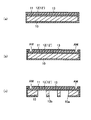
また、図3は上記の生産用マスクの模式断面図である。
シリコン基板10上に、エッチングストッパ機能を有する中間層である埋め込み酸化膜(BOX:buried oxide)11およびメンブレンになるシリコンの第1薄膜(SOI:silicon on insulator)12が形成された積層構造を有する。メンブレンに対応する部分のシリコン基板10は裏面からエッチングされて格子状に区画された凹部10aが形成され、格子状の梁10bが構成されている。
格子状の梁10bで区分された凹部10a領域におけるSOI層12には、マスクパターンに沿った貫通孔Pが形成されている。
ここで、小画メンブレン領域となる凹部10aを区画する格子状の梁10bの形成領域において、SOI層10に第1位置精度計測用マークMK1が形成されている。
【0036】
また、図4は上記の生産用マスクの位置精度計測用マークのレイアウトを示す平面図である。
小画メンブレン領域となる凹部10aを区画する格子状の梁10bの形成領域において、第1位置精度計測用マークMK1が形成されている。
【0037】
ここで、第1位置精度計測用マークMK1は格子状の梁10bの形成領域であれば、図3に示すように梁10bの上方のSOI層12に形成されていても、SOI層12の形成面側とは反対側の面における梁10bの表面に形成されていてもよく、例えば第1位置精度計測用マークMK1の位置を計測するときの姿勢に応じて選択することができる。
図3に示すマスクパターンに沿った貫通孔Pについては、図4では省略している。
【0038】
一方、位置精度計測用マスクは上記の生産用マスクと同様の構成であるが、凹部10a領域におけるSOI層にマスクパターンに沿った貫通孔が形成されている代わりに第3位置精度計測用マークMK3が形成されていることが異なる。
位置精度計測用マスクについて図3および図4を用いて説明する。
即ち、シリコン基板10上にBOX層11および第2薄膜(SOI)12’が積層しており、メンブレンに対応する部分のシリコン基板は裏面からエッチングされて格子状に区画された凹部10aが形成され、格子状の梁10bが構成されている。
ここで、図4に示すように、格子状の梁10bの形成領域において、第1位置精度計測用マークMK1と同様に、第2位置精度計測用マークMK2が形成されている。
また、格子状の梁10bで区分された凹部10a領域におけるSOI層12’には第3位置精度計測用マークMK3が形成されており、図4においては詳細な図示を省略している。
【0039】
上記の第1位置精度計測用マークMK1および第2位置精度計測用マークMK2としては、例えば1つの凹部として区画された領域の周囲の梁10bの形成領域に20個のマークが形成されている。このように、図16に示す従来例におけるマークの数よりも大幅に多くのマークを配置することができ、これによってより高次の歪も計測でき、線形成分以外の高次の項まで補正できるようになる。
また、第3位置精度計測用マークMK3としては、格子状に区画された1つの凹部10a領域ごとに、例えば6μm角の正方形マークが500μmピッチで3×3個配置されている。
【0040】
次に、上記のような構成の生産用マスクと位置精度計測用マスクの製造方法について説明する。例えば、特許文献1や本願出願人による出願(特願2001−370600号)に詳しく述べられている方法を好ましく採用することができる。
生産用マスクにおいては凹部10a領域におけるSOI層にマスクパターンに沿った貫通孔を形成し、位置精度計測用マスクにおいては第3位置精度計測用マークMK3を形成することを除いて、生産用マスクと位置精度計測用マスクは同様に形成することができる。
【0041】
まず、図5(a)に示すように、例えばシリコン基板10上に、エッチングストッパ機能を有する中間層である埋め込み酸化膜(BOX層)11とメンブレンになるシリコン層(SOI層)12が積層して形成されたSOIウェハを準備する。SOIウェハの表面全体は自然酸化膜13で被覆されている。
上記の構成のSOIウェハに、ホウ素(B)を注入することで、メンブレン層の内部応力を調整する。
【0042】
次に、図5(b)に示すように、例えばSOIウェハの周辺部において、所定のパターンでBOX層11に達するまでSOI層12を除去し、アライメントマークAMを形成する。
【0043】
次に、図5(c)に示すように、シリコン基板の裏面上にレジスト膜(不図示)を成膜し、格子状のパターンに開口するように露光および現像し、RIE(反応性イオンエッチング)などのエッチング処理を行って、例えば格子状に区画されたパターンでシリコン基板10の裏面からBOX層11に達する凹部10aを形成する。このとき、シリコン基板10の格子状に残された部分が格子状の梁10bとなり、SOIウェハの周辺部においては、シリコン基板10が支持枠となる。
【0044】
次に、図6(a)に示すように、レジスト膜(不図示)をアッシング処理などにより除去し、HF液によるウェットエッチングにより表面に露出した部分の酸化シリコンを除去する。即ち、自然酸化膜13と、凹部10a底部に露出したBOX膜11を除去する。
以上で、シリコン基板10上にBOX層11およびSOI層12が積層され、シリコン基板10裏面側からSOI層が露出するまで格子状に区画された凹部が形成されてなるマスクブランクスが形成される。
【0045】
次に、図6(b)に示すように、SOI層12の上層にレジスト膜Rを成膜し、生産用マスクの製造方法においては、形成しようとするマスクのマスクデータに沿って、例えば電子線露光などにより露光し、現像してパターンPを形成する。同時に、レジスト膜Rには第1位置精度計測用マークMK1についてもパターンを形成する。
【0046】
次に、レジスト膜RをマスクとしてRIEなどのドライエッチングを施し、生産用マスクの製造方法においては、SOI層12に形成しようとするマスクのパターンPと第1位置精度計測用マークMK1を転写する。
この後、レジスト膜Rをアッシング処理による除去して、図6(c)に示す構成のマスクを製造することができる。
【0047】
一方、位置精度計測用マスクの製造方法においては、上記の生産用マスクの製造方法と同様にして、図6(a)に示すように、シリコン基板10上にBOX層11およびSOI層12’が積層されたマスクブランクスろ形成し、図6(b)に示すように、第2位置精度計測用マークMK2および第3位置精度計測用マークMK3のパターンに沿って露光し、現像して第2位置精度計測用マークMK2および第3位置精度計測用マークMK3のパターンを得る。
次に、図6(c)に示すように、SOI層12’に第2位置精度計測用マークMK2および第3位置精度計測用マークMK3のパターンを転写する。
【0048】
本実施形態においては、上記のように形成した生産用マスクと位置精度計測用マスクを用いて、図1のフローチャートに示す手順により生産用マスクの歪データを生成することができる。このようにして生成されたマスク歪データは、後述の理由から歪計測の正確さを向上させることができる。
【0049】
次に、得られた生産用マスクの歪データから、この生産用マスクを用いてパターンを露光するときにマスク歪をより精密に補正しながらパターン露光することができる露光方法について説明する。
【0050】
図7はLEEPLに用いる露光システムの概略図である。
この露光システムは、電子銃30、アパーチャー31、コンデンサレンズ32、一対の主偏向レンズ(33,34)および一対の副偏向レンズ(35,36)を有する。
【0051】
電子銃30から、例えばEB加速電圧2keVで加速され、電流値5.5μA、ビーム径300μmの電子ビームEBが出射され、アパーチャー31により径が制限され、コンデンサレンズ32により平行なビームにされる。
主偏向レンズ(33,34)は、電子ビームEBが平行なままステンシルマスク37に垂直に入射するように、電子ビームEBを偏向させる。
電子ビームEBはラスターまたはベクトル走査モードのいずれかでステンシルマスク37に入射するが、いずれの場合も電子ビームEBの偏向に主偏向レンズ(33,34)が用いられる。副偏向レンズ(35,36)は主偏向レンズ(33,34)によって偏向された電子ビームEBをさらに微調整する。
ステンシルマスク37を透過した電子ビームEBは、例えばシリコンウェーハ38上に設けられたレジスト膜39に照射され、パターン露光される。
本実施形態においては、得られた生産用マスクの歪データから、この生産用マスクを用いて、例えば副偏向レンズ(35,36)の条件を補正し、この補正した条件で露光することでマスク歪をより精密に補正しながらパターン露光することができる。
【0052】
(実施例)
ここでは、本実施形態のマスク歪データの生成方法をPELマスクに適用して、マスク歪データを生成した。
まず以下のようにして、生産用マスクと位置精度計測用マスクを形成した。
マスクブランクス製造用の基板として、貼り合わせ法により作製された市販の4インチ(約100mm)のSOIウェハを用いた。ウェハ基板の厚みは381μm(マスクの平坦度を向上させるために両面研磨)、BOX層の厚みは400nm、SOI層の厚みは600nmであり、SOI層に1019/cm3 のホウ素(B)原子を注入することで、メンブレン層の内部応力を10MPaに調整した。
上記の構成のSOIウェハに対して、図5(a)〜(c)および図6(a)〜(c)に示す工程により、図2および図3に示す構成の生産用マスクと位置精度計測用マスクを形成した。
ここで、生産用マスクにおける第1位置精度計測用マークMK1と位置精度計測用マスクにおける第2位置精度計測用マークMK2は同一の構成として、梁10bの形成領域に形成した。
一方、生産用マスクにおいては格子状に区画された凹部領域におけるSOI層に、形成しようとするマスクのパターンPを転写し、一方、位置精度計測用マスクにおいては、第3位置精度計測用マークのパターンを転写した。
【0053】
以降の工程において、生産用マスクと位置精度計測用マスクは図8(a)および(b)に示すアルミニウム製フレームに接着して使用した。
図8(a)は上記のフレームの平面図であり、図8(b)は断面図である。
フレーム20は外周20aおよび内周20bを有するリング状であり、所定の径の位置で段差20cが形成されている。一辺2Lのマスク領域全体よりも広くなるように内径が設計されている。
上記のフレームに対して、段差20cよりもやや内側の領域の円周上の120°おきの3点においてエポキシ樹脂で生産用マスクと位置精度計測用マスクのそれぞれを接着した。
【0054】
次に、まず位置精度計測用マスクについて、座標測定器(LMS IPRO)により格子状の梁の形成領域に形成された第2位置精度計測用マークと格子状の梁によって区画された凹部の形成領域におけるSOI層に形成された第3位置精度計測用マークの位置をそれぞれ計測して、第2位置精度計測用マークのIPデータと第3位置精度計測用マークのIPデータを取得した。
ここで、座標測定器で位置計測を行うにあたって、位置精度計測用マスクと生産用マスクの位置精度を計測できるように、新たにマスク保持用カセットを製作した。
図9(a)はマスク保持用カセットの平面図であり、図9(b)はマスク保持用カセットでマスクを保持したときの模式断面図である。
マスク保持用カセット21には、静電チャック21aが設けられており、それによりマスク領域21b(この場合中心40mm角)以外の外周部を静電チャックするようになっており、SOI層(第2薄膜)12’が上側を向くようにして、SOI層(第2薄膜)12’の反対側からマスクを保持した状態で計測する。尚、図9(b)においては第2位置精度計測用マークの図示を省略している。
また、静電チャックではなく吸引チャックが設けられている構成としてもよい。
これにより、ステンシルマスクを平坦化した状態で、マークのIP精度を測定することができる。
【0055】
ここで、梁の形成領域に形成した第2位置精度計測マークMK2と格子状に区画された凹部領域におけるSOI層に形成した第3位置精度計測用マークMK3の計測結果について、説明する。
図10(a)は梁の形成領域に形成した第2位置精度計測マークMK2の計測結果を示すグラフであり、実線は実測値を繋いだ線であり、破線は理想的な格子位置を示す線である。
尚、ここでは理想格子からのズレを見やすくするために、誤差は拡大して図示している。
【0056】
一方、図10(b)は格子状に区画された凹部領域におけるSOI層に形成した第3位置精度計測用マークMK3の計測結果を示すグラフであり、実線は実測値を繋いだ線であり、破線は理想的な格子位置を示す線である。
【0057】
この図から分かるとおり、梁の形成領域に形成した第2位置精度計測マークMK2と格子状に区画された凹部領域におけるSOI層に形成した第3位置精度計測用マークMK3のIP計測結果は類似しており、定性的には従来技術(特許文献6)の考え方を支持しているように見えるが、詳細にデータを解析すると、両者には最大約20nmの差異があることが分かった。
この誤差は、EPLのような1/4縮小投影法では5nm、PELでは20nmの誤差をウエハ上で生じる。従来技術は1/4縮小投影法ですら許容できない誤差を生じるのであるから、本実施例で用いた等倍法のPELで用いることはできない。
【0058】
この誤差の原因としては次のことが考えられる。
梁の形成領域に形成した第2位置精度計測マークMK2と格子状に区画された凹部領域におけるSOI層に形成した第3位置精度計測用マークMK3を同じ描画および加工プロセスで形成する場合、そのIP誤差は主としてEB描画機の精度で規定されるので、両者は類似するはずである。
しかし、EB描画機と座標測定器のステージにマスクを固定する場合、2つのステージで固定方法が厳密には同一ではないために、マスクの反りが矯正される度合いの相違により、マスクの形状(凹凸)が異なる。
梁の形成領域に形成した第2位置精度計測マークMK2は基本的に、材料力学の文献に述べられているように(例えば、非特許文献4(S. P. Timoshenko and S. Woinowsky-Krieger,“Theory of Plates and Shells ”)参照)、(マスク基板の傾斜角)×(基板厚さの半分)の面内変位を示す。
一方、格子状に区画された凹部領域におけるSOI層に形成した第3位置精度計測用マークMK3は、凹部領域を取り囲む梁の変形を強制変位(境界条件)と考えた時に、SOI層内部で誘起される変位にしたがう。
上記のように、変位のメカニズムが異なるのだから、図10(a)および(b)に示したように両者が異なるのは物理的に当然である。
【0059】
本実施例においては、次に、図10(a)および(b)に示す2つのデータから、第2位置精度計測用マークのIPデータと第3位置精度計測用マークのIPデータ間の相関関数を算出した。
本実施例では相関関数を実験的に算出したが、このプロセスを高精度な有限要素シミュレーションで代用することもできる。
【0060】
次に、図9(a),(b)に示すように、位置精度計測用マスクの場合と同様にして、生産用マスクについて、座標測定器(LMS IPRO)により格子状の梁の形成領域に形成された第1位置精度計測用マークを計測して、第1位置精度計測用マークのIPデータを取得した。尚、図9(b)においては第1位置精度計測用マークの図示を省略している。
ここで、生産用マスクの計測にあたり、位置精度計測用マスクの計測で使用したものと同じカセットを用いて生産用マスクを保持した。
【0061】
生産用マスクにおいて梁の形成領域に形成した第1位置精度計測マークMK1の計測結果について説明する。
図11は梁の形成領域に形成した第1位置精度計測マークMK1の計測結果を示すグラフであり、実線は実測値を繋いだ線であり、破線は理想的な格子位置を示す線であり、上記と同様、理想格子からのズレを見やすくするために、誤差は拡大して図示している。
【0062】
上記のようにして第1位置精度計測用マークのIPデータを取得した後、上記のようにして求めた第2位置精度計測用マークのIPデータと第3位置精度計測用マークのIPデータ間の相関関数を用いて、生産用マスクのSOI層におけるマスク歪データを生成した。
【0063】
次に、上記で得られた生産用マスクのSOI層におけるマスク歪データを用いて、LEEPL転写装置の副偏向補正データを作成した。
得られた副偏向補正データに従ってArFリソグラフィで形成した下地回路パターン上にPELでパターンを転写したところ、重ね合せ精度が平均50nm(3σ)から28nmに劇的に改善し、本実施形態に係るマスクの歪データの生成方法とこれを用いた露光方法が転写IP精度の向上に極めて有効であることが証明された。
【0064】
上記のように、本実施形態においては、位置精度計測用マスクにおける梁の形成領域に形成した第2位置精度計測マークMK2と格子状に区画された凹部領域におけるSOI層に形成した第3位置精度計測用マークMK3から得られる歪関数の相関をあらかじめ調べておき、生産用マスクにおいて、梁の形成領域に形成した第1位置精度計測マークMK1のIP誤差を生産用マスクのSOI層におけるパターンのIP誤差に変換してから用いる。
これにより、得られたパターンのIP誤差からこの生産用マスクを用いてパターンを露光するときのEB偏向条件などの露光装置の条件を補正し、マスク歪をより精密に補正しながらパターン露光することができる。
【0065】
第2実施形態
第1実施形態の補正精度をさらに向上させるため、生産用マスクのSOI層(第1薄膜)におけるマスク歪データを生成した後、位置精度計測用マスクと生産用マスクのそれぞれにおいて、第2薄膜および第1薄膜が上側を向いた状態から下側を向くようにしたときの位置精度計測用マスクおよび生産用マスクに発生する歪を示す関数を用いてマスク歪データを補正することが好ましい。
位置精度計測時と露光時とでマスクの上下位置が反転し、重力によるマスクのグローバルな変形によってIP誤差が生じる。このため、あらかじめ上下反転によるIPシフトを記述するパターン像伝達関数(ITF:image transfer function )を求めておき、その関数でマスクデータをシフトさせておくものである。なお、この方法についての詳細は、本願発明の出願人による特許出願(特願2002−092612号)に記載されている。
第1実施形態において得られる生産用マスクの歪データはSOI層が上側と向いた状態でのデータなので、実際の露光工程においてはSOI層が下側と向いた状態で用いることから、ITFで下向きのデータに換算してから副偏向補正データを作成すれば、さらに精度は向上する。
【0066】
第3実施形態
第2実施形態では、マスクのIP測定時と露光時のマスク姿勢の反転をITFで補正しているが、別の方法として、マスクのIP測定工程においてマスクの姿勢を露光時と同じ姿勢として行う方法がある。
即ち、位置精度計測用マスクおよび生産用マスクに対して、第1〜第3位置精度計測用マーク(MK1〜MK3)の位置計測を行うときに、第1薄膜あるいは第2薄膜が下側を向くように配置した姿勢でカセットに保持すれば、露光工程と同じ第1薄膜あるいは第2薄膜が下側を向いた姿勢での位置計測が可能となり、この状態で位置を計測すれば第2実施形態で示したITF関数を用いずにより正確に位置計測を行い、マスクの歪関数を生成することができる。
PELとEPLの露光装置では、マスクは下向きに実装されるが、静電チャックする面が異なるので、できる限り露光姿勢と同じ状態で位置計測を行うためには、それぞれで別設計のカセットを用いることが望ましい。
【0067】
図12はEPL用マスクに対するマスク保持用カセットでPEL用マスクを保持したときの模式断面図である。
マスク保持用カセット22には、静電チャック22aが設けられており、また、マスク領域には凹部22bが形成されており、凹部を除く外周部を静電チャックするようになっている。
ここで、マスクのSOI層(12,12’)が下側を向くようにして、SOI層(12,12’)側から保持した状態で計測する。尚、図12においては第1および第2位置精度計測用マークの図示を省略している。
また、静電チャックではなく吸引チャックが設けられている構成としてもよい。
EPL用マスクにおいて、露光工程におけるマスクの姿勢と保持状態を再現してIP計測を行うことで、より精密に歪データを生成することができる。
【0068】
図13はPEL用マスクに対するマスク保持用カセットでPEL用マスクを保持したときの模式断面図である。
マスク保持用カセットには、静電チャック23aが設けられており、それによりマスク領域23b以外の外周部を静電チャックするようになっており、マスクのSOI層(12,12’)が下側を向くようにして、SOI層(12,12’)とは反対側から保持され、ケース24に挿入された状態で計測する。尚、図13においては第1および第2位置精度計測用マークの図示を省略している。
また、静電チャックではなく吸引チャックが設けられている構成としてもよい。
PEL用マスクにおいて、露光工程におけるマスクの姿勢と保持状態を再現してIP計測を行うことで、より精密に歪データを生成することができる。
【0069】
本実施形態のマスク歪データの生成方法と、これを用いた露光方法によれば、以下の効果を享受できる。
1.PELとEPLにおいて、生産用マスクに対して、デバイスパターンと干渉しない梁の形成領域内に形成された位置精度計測用マークにより、マスク歪が正確に計測できるようになる。
2.マスク歪が正確に計測できるようになることで、電子光学系の副偏向によるパターン位置補正の精度が向上する。
3.パターンの転写位置精度が向上することで、製造されるデバイスの歩留が向上する。
4.パターン位置補正精度が向上することで、マスク製造に対する位置精度要求仕様を緩和でき、マスクコストが低減し、デバイス製造コストが下がる。
【0070】
上記の本実施形態のマスクの製造方法を半導体装置の製造方法に適用することができる。
即ち、本実施形態に係るマスクの歪データの生成方法により、生産用マスクの歪データを算出する。
次に、得られた歪データを補正するようにEBの副偏向レンズの補正条件を求め、この生産用マスクを用いてパターン露光し、マスクに形成されたパターンを感光面に転写する。
以上で、本実施形態のマスクの製造方法を適用して、半導体装置を製造することができる。
【0071】
本発明は、上記の実施形態に限定されない。
例えば、本実施形態においては、ステンシルマスク(PELマスク)について説明したが、各種論文および特許により公知となっているマスク製造プロセスを適用することにより、各NGL用のマスクとすることができ、例えば、本発明はPELマスクに限らず、EPLマスクへの適用が可能である。
また、本発明のマスクの歪データの生成方法や露光方法は、被露光ウエハにパターン露光する工程を有する半導体装置の製造方法において、パターン露光するためのマスクに対する歪データの生成方法やそれを用いた露光方法として適用できる。
その他、本発明の要旨を逸脱しない範囲で種々の変更が可能である。
【0072】
【発明の効果】
本発明のマスクの歪データの生成方法は、歪計測の正確さを向上させることができる。
【0073】
本発明の露光方法は、本発明のマスクの歪データの生成方法を用いてマスク歪をより精密に補正して露光することができる。
【0074】
本発明の半導体装置の製造方法は、本発明のマスクの歪データの生成方法とこれを用いた露光方法を用いて半導体装置を製造することができる。
【図面の簡単な説明】
【図1】図1は第1実施形態に係るマスク歪データの生成方法と、これを用いた露光方法を示すフローチャートである。
【図2】図2(a)は第1実施形態に係る生産用マスクおよび位置精度計測用マスクの外観を示す平面図であり、図2(b)は、図2(a)のマスク領域の中央部を拡大した図である。
【図3】図3は第1実施形態に係る生産用マスクおよび位置精度計測用マスクの模式断面図である。
【図4】図4は第1実施形態に係る生産用マスクおよび位置精度計測用マスクの位置精度計測用マークのレイアウトを示す平面図である。
【図5】図5(a)〜(c)は、第1実施形態に係る生産用マスクと位置精度計測用マスクの製造方法を示す断面図である。
【図6】図6(a)〜(c)は、第1実施形態に係る生産用マスクと位置精度計測用マスクの製造方法を示す断面図である。
【図7】図7はLEEPLに用いる露光システムの概略図である。
【図8】図8(a)は実施例1において用いたフレームの平面図であり、図8(b)は断面図である。
【図9】図9(a)は実施例1に係るマスク保持用カセットの平面図であり、図9(b)はマスク保持用カセットでマスクを保持したときの模式断面図である。
【図10】図10(a)は梁の形成領域に形成した第2位置精度計測マークの計測結果を示すグラフであり、図10(b)は格子状に区画された凹部領域におけるSOI層に形成した第3位置精度計測用マークの計測結果を示すグラフである。
【図11】図11は梁の形成領域に形成した第1位置精度計測マークの計測結果を示すグラフである。
【図12】図12は第3実施形態に係るマスク保持用カセットでマスクを保持したときの模式断面図である。
【図13】図13は第3実施形態に係るマスク保持用カセットでマスクを保持したときの模式断面図である。
【図14】図14は従来例に係る格子状の梁を有するマスクの模式斜視図である。
【図15】図15(a)は従来例に係るステンシルマスクの模式断面図であり、図15(b)は従来例に係る散乱メンブレンマスクの模式断面図である。
【図16】図16は従来例に係るスクライブラインに座標計測用マークを配置しているレイアウトの例である。
【符号の説明】
10…シリコン基板、10a…凹部、10b…梁、11…BOX層、12,12’…SOI層、13…自然酸化膜、20…フレーム、20a…外周、20b…内周、20c…段差、21,22,23…マスク保持用カセット、21a,22a,23a…静電チャック、21b…マスク領域、22b…凹部、24…ケース、30…電子銃、31…アパーチャー、32…コンデンサレンズ、33,34…主偏向レンズ、35,36…副偏向レンズ、37…ステンシルマスク、38…シリコンウェハ、39…レジスト膜、100a…凹部、100b…梁、102…薄膜、110…基板、110a…凹部、110b…梁、111…埋め込み酸化物層、112…SOI層、120…シリコン基板、120a…凹部、120b…梁、121…薄膜、122…クロム膜、123…タングステン膜、124…散乱体パターン、EB…電子ビーム、AM…アライメントマーク、PA…パターン領域、P…パターン、MK1…第1位置精度計測用マーク、MK2…第2位置精度計測用マーク、MK3…第3位置精度計測用マーク、MK…座標計測用マーク、CR…チップ領域、SL…スクライブライン、ST11〜ST21…ステップ。[0001]
BACKGROUND OF THE INVENTION
The present invention relates to a mask distortion data generation method used in a lithography process for manufacturing a semiconductor device, an exposure method using the mask distortion data, and a semiconductor device manufacturing method using the method.
[0002]
[Prior art]
EB (electron beam) and ions that are being developed as next generation lithography (NGL) following photolithography (wavelengths of 248 nm and 193 nm are mainly used) for mass production of semiconductor devices. Masks used for lithography using charged particles called beams have common points.
The mask blanks, which are masks before the pattern is formed, are etched deeply from the back side so as to leave a thin film (membrane) having a thickness of about 10 nm to 10 μm with respect to the substrate serving as a mask. Forming and arranging the pattern to be transferred on the obtained thin film.
Since these masks include a membrane region with low mechanical rigidity, the mask distortion is measured as well as a method for forming a pattern with high position accuracy (IP: image placement), and the IP error is measured using the information. It is important to have a technique for correcting the above.
[0003]
Prominent electron beam lithography (PEL) and electron projection lithography (EPL) are particularly prominent among NGLs using EB.
For these two methods, general explanations such as electron optical systems and masks are described in
[0004]
Among the masks used for the above-mentioned PEL and EPL, those in which the transfer pattern is formed by the opening of the membrane (1) is formed by a stencil mask (for example, see Non-Patent Document 2), (2) a scatterer such as a metal thin film What is done is called a scattering membrane mask (see Non-Patent Document 3, for example).
The former stencil mask is used for both PEL and EPL, while the scattering membrane mask cannot be used for PEL. This is because, since PEL generally uses a low-speed EB of several keV or less, all EB incident on the membrane is absorbed.
[0005]
Since these masks include a membrane region with low mechanical rigidity, the entire mask region is not composed of a single membrane, but a mask structure composed of a large number of small membrane membranes divided by lattice beams. For example,
FIG. 14 is a schematic perspective view of a mask having the lattice-like beam described above. A plurality of
[0006]
As a method for manufacturing a mask having the beam structure described above, Patent Document 3 describes a method using wet etching with an alkaline solution such as KOH or a method using reactive ion etching.
[0007]
FIG. 15A is a schematic cross-sectional view of the stencil mask.
The
In addition, a through hole P is formed in the
[0008]
FIG. 15B is a schematic sectional view of the scattering membrane mask.
A silicon nitride
On the
[0009]
As a method of transferring a mask pattern used for PEL or EPL to a wafer with high accuracy, it is conceivable to measure the distortion of the mask and correct it at the time of transfer.
The concept itself is not new and has been used in photolithography, and the IP accuracy of the photomask produced is routinely measured by a coordinate measuring instrument called LEICA LMS IPRO or Nikon's lightwave XY-6i. Has been measured.
[0010]
For example, if a magnification error of 3 ppm is measured in the mask pattern, when the photomask is exposed with a stepper or scanner, the optical error of the exposure apparatus can be finely adjusted to correct the magnification error.
[0011]
However, in lithography using charged particles such as PEL and EPL, it is considered that incident particles can be deflected with high accuracy and high speed by an electrostatic / magnetic field lens, so that more advanced correction is possible.
[0012]
In the case of PEL, EB is deflected by combining a main deflection lens and a sub deflection lens. Here, the mask distortion can be corrected by scanning the EB over the mask region with the main deflection lens and changing the incident angle of the EB in real time with the sub deflection lens (see, for example, Patent Document 4).
On the other hand, in the case of EPL, each membrane separated by the
[0013]
In the case of PEL, distortion information over the entire mask is given as a map, and interpolation between measurement data points is performed with a high-order function, so that not only linear distortion such as magnification, rotation, and orthogonality, but also higher-order distortion can be obtained. There is an advantage that it can be corrected.
On the other hand, in the case of EPL, only linear distortion for each subfield can be corrected.
[0014]
In any of the PEL and EPL methods described above, it is important to first accurately measure the mask distortion. However, generally, a mark for a coordinate measuring instrument such as the aforementioned LMS IPRO cannot be arranged in an area where a device pattern is arranged.
Therefore, in the case of a photomask, coordinate measurement marks are arranged in a portion corresponding to a chip peripheral area (margin area when a chip on a wafer is cut by dicing), which is called a scribe line.
FIG. 16 is an example of a layout in which coordinate measurement marks are arranged on a scribe line. A coordinate measurement mark MK is arranged on a scribe line SL that divides the chip region CR.
Although it is more reliable to increase the number of coordinate measurement marks to increase the number of measurement points and distribute evenly over the entire mask area, the reliability of distortion data is improved, but the coordinate measurement marks can only be placed on the scribe line. Due to the restrictions, only a limited number of coordinate measurement marks can be used as shown in FIG.
[0015]
In EPL, coordinate measurement is performed on the beam between subfields by utilizing the fact that the mask is originally divided into subfields (typically about 1 mm square) as shown in FIG. It has been proposed to place a mark for use (see Patent Document 6).
As described above, since EPL corrects only the linear distortion of the subfield, it is sufficient to measure the mark coordinates of the four corners of each subfield. Since the marks on the beam are not transferred onto the wafer, the number of measurement points can be increased and the strain measurement accuracy can be improved. Patent Document 6 discloses a method for forming and arranging on-beam marks.
[0016]
[Patent Document 1]
JP 2003-59819 A
[Patent Document 2]
US Pat. No. 5,523,580
[Patent Document 3]
US Pat. No. 6,428,937
[Patent Document 4]
U.S. Pat. No. 4,334,156
[Patent Document 5]
JP 2000-124114 A
[Patent Document 6]
US Pat. No. 6040095 specification
[Non-Patent Document 1]
T.A. T. Utsumi, “Journal of Vacuum Science and Technology” B17, p. 2897 (1999)
[Non-Patent Document 2]
H. C. HC Pfeiffer, “Japanese Journal of Applied Physics” 34, p. 6658 (1995)
[Non-Patent Document 3]
L. R. Harriott, “Journal of Vacuum Science and Technology” B15, p. 2130 (1997)
[Non-Patent Document 4]
S. P. T. P. Timochenko and S. Timochenko S. winsky-Krieger, “Theory of Plates and Shells”
[0017]
[Problems to be solved by the invention]
However, the method described in Patent Document 6 described above has a limit in the accuracy of strain measurement and is difficult to use for device production using PEL or EPL.
That is, the method of Patent Document 6 is based on the assumption that the latter displacement can be corrected by the former measurement data because the on-beam mark and the actual device pattern in the membrane are displaced by the same strain function. . However, it has become clear that this assumption is not physically self-explanatory and that it can only be approximated in our measurements.
Therefore, more accurate measurement of the membrane strain cannot be performed only by measuring the mark on the beam. In particular, in the case of PEL, since the pattern on the mask is transferred onto the wafer without being reduced, it is considered that the influence of the distortion data error is larger than that of EPL. Therefore, it is difficult to apply the method described in Patent Document 6 as it is.
[0018]
The present invention has been made in view of the above problems. Therefore, the present invention provides a mask distortion data generation method capable of improving the accuracy of distortion measurement, and more accurately mask distortion using the method. It is an object of the present invention to provide an exposure method capable of correcting exposure and a method for manufacturing a semiconductor device using the exposure method.
[0019]
[Means for Solving the Problems]
In order to achieve the above object, a mask strain data generation method according to the present invention includes at least one first thin film in which a transmission part and a blocking part of a charged particle beam are formed in a predetermined pattern, and the first position A method of generating mask strain data in the first thin film of a production mask on which an accuracy measurement mark is formed, wherein the first position accuracy measurement is substantially performed on a mask blank having at least one second thin film. Forming a second position accuracy measurement mark at the same position as the mark for use and forming a third position accuracy measurement mark on the second thin film to form a position accuracy measurement mask; and the position accuracy measurement mask. Measuring the positions of the second position accuracy measurement mark and the third position accuracy measurement mark, and the second position accuracy measurement mark and the third position accuracy measurement mark of the position accuracy measurement mask. A step of calculating a correlation function between positions; a step of measuring a position of the first position accuracy measurement mark of the production mask; and a position of the first position accuracy measurement mark of the production mask. Generating mask strain data in the first thin film of the production mask using a correlation function.
[0020]
The mask strain data generation method of the present invention described above has at least one first thin film in which a charged particle beam transmission part and a blocking part are formed in a predetermined pattern, and a first position accuracy measurement mark is formed. This is a method for generating mask strain data in the first thin film of the produced production mask.
A second position accuracy measurement mark is formed on the mask blank having at least one layer of the second thin film substantially at the same position as the first position accuracy measurement mark, and the third position accuracy measurement mark is formed on the second thin film. Form a mask for position accuracy measurement.
Next, the positions of the second position accuracy measurement mark and the third position accuracy measurement mark of the position accuracy measurement mask are measured, and between the positions of the second position accuracy measurement mark and the third position accuracy measurement mark are measured. Calculate the correlation function.
Next, the position of the first position accuracy measurement mark of the production mask is measured.
Next, mask distortion data in the first thin film of the production mask is generated from the position of the first position accuracy measurement mark of the production mask using the correlation function.
[0021]
In order to achieve the above object, an exposure method of the present invention includes at least one first thin film in which a charged particle beam transmitting portion and a blocking portion are formed in a predetermined pattern, and a first position accuracy measurement mark. The pattern is exposed to light using a production mask formed with a mask blank having at least one second thin film, and the second is substantially at the same position as the first position accuracy measurement mark. Forming a position accuracy measurement mark and forming a third position accuracy measurement mark on the second thin film to form a position accuracy measurement mask; and for the second position accuracy measurement of the position accuracy measurement mask. A step of measuring the position of the mark and the third position accuracy measurement mark, and a correlation function between the position of the second position accuracy measurement mark and the position of the third position accuracy measurement mark of the position accuracy measurement mask. Mechanic to calculate Measuring the position of the first position accuracy measurement mark on the production mask, and using the correlation function from the position of the first position accuracy measurement mark on the production mask. Generating mask distortion data in the first thin film; and exposing the pattern using the production mask while correcting the mask distortion in the first thin film.
[0022]
In the above-described exposure method of the present invention, after generating mask strain data by the above-described mask strain data generation method of the present invention, the pattern is exposed using the production mask while correcting the mask strain in the first thin film. .
[0023]
In order to achieve the above object, a method of manufacturing a semiconductor device according to the present invention includes a first thin film having at least one layer in which a transmission part and a blocking part of a charged particle beam are formed in a predetermined pattern. A method for manufacturing a semiconductor device comprising a step of exposing the pattern to a wafer to be exposed using a production mask on which a measurement mark is formed, wherein the mask blank having at least one second thin film is substantially applied to the mask blank. Forming a second position accuracy measurement mark at the same position as the first position accuracy measurement mark and forming a third position accuracy measurement mark on the second thin film to form a position accuracy measurement mask; Measuring the position of the second position accuracy measurement mark and the third position accuracy measurement mark of the position accuracy measurement mask; the second position accuracy measurement mark of the position accuracy measurement mask; A step of calculating a correlation function between the positions of the position accuracy measurement marks, a step of measuring a position of the first position accuracy measurement marks of the production mask, and the first position accuracy measurement of the production mask. Generating mask distortion data in the first thin film of the production mask from the position of the production mark using the correlation function, and correcting the mask distortion in the first thin film while using the production mask. Exposing the pattern to an exposure wafer.
[0024]
In the method of manufacturing a semiconductor device of the present invention described above, the mask strain data is generated by the above-described mask strain data generation method of the present invention, and then the mask is corrected using the production mask while correcting the mask strain in the first thin film. Exposing the pattern to an exposure wafer.
[0025]
DETAILED DESCRIPTION OF THE INVENTION
Hereinafter, a mask strain data generation method, an exposure method using the mask strain data generation method, and a semiconductor device manufacturing method according to the present embodiment will be described with reference to the drawings.
[0026]
First embodiment
The present embodiment relates to a method for generating strain data in a mask such as a PEL mask for exposure using a LEEPL transfer apparatus, and includes at least a first layer in which a charged particle beam transmitting portion and a blocking portion are formed in a predetermined pattern. This is a method for generating mask strain data relating to a pattern provided on a first thin film in a production mask having one thin film and having a first position accuracy measurement mark formed thereon.
The present embodiment is a method for exposing a pattern by correcting the distortion from the mask distortion data using the mask.
[0027]
FIG. 1 is a flowchart showing a mask distortion data generation method according to the present embodiment and an exposure method using the method.
First, as a first step ST11, a mask for measuring position accuracy is formed from a mask blank having at least one second thin film.
Here, the position accuracy measurement mask has the same configuration as the production mask except that a position accuracy measurement mark is formed on the second thin film instead of the pattern formed on the first thin film. . That is, the first thin film and the second thin film have the same layer structure, and the second position accuracy measurement mark is formed on the position accuracy measurement mask substantially at the same position as the first position accuracy measurement mark. The second thin film is formed with a third position accuracy measurement mark instead of a pattern.
[0028]
Next, as the second step ST12, for example, the positions of the second position accuracy measurement mark and the third position accuracy measurement mark of the position accuracy measurement mask are measured by a coordinate measuring instrument such as LMS IPRO, and the third step IP data of the second position accuracy measurement mark is acquired as ST13, and IP data of the third position accuracy measurement mark is acquired as fourth step ST14.
[0029]
Next, as a fifth step ST15, a correlation function between the IP data of the second position accuracy measurement mark and the IP data of the third position accuracy measurement mark is calculated.
Here, the steps from the first step ST11 to the fifth step ST15 can be substituted by a finite element simulation in which a mask is modeled.
[0030]
On the other hand, as a sixth step ST16, a production mask is formed from mask blanks having at least one first thin film.
Here, the first position accuracy measurement mark is formed on the production mask as described above, and the transmission part and the blocking part of the charged particle beam are formed in a predetermined pattern on the first thin film.
[0031]
Next, as the seventh step ST17, as in the second step ST12, the position of the first position accuracy measurement mark on the production mask is measured by a coordinate measuring instrument such as LMS IPRO, and the eighth step ST18 is performed. Obtain IP data of the mark for 1-position accuracy measurement.
[0032]
Next, as a ninth step ST19, a seventh step ST17 is performed by using a correlation function between the IP data of the second position accuracy measurement mark and the third position accuracy measurement mark obtained in the fifth step ST15. Mask distortion data in the first thin film of the production mask is generated from the IP data of the first position accuracy measurement mark obtained in the above.
As described above, mask distortion data relating to the pattern provided on the first thin film in the production mask in which the first position accuracy measurement mark is formed is generated.
[0033]
Further, in order to expose a pattern using the production mask described above, the following is performed.
That is, as the 10th step ST20, the exposure apparatus conditions such as the EB deflection condition when the pattern is exposed using the production mask are corrected from the mask distortion data in the first thin film of the production mask obtained above. To do.
Next, as an eleventh step ST21, pattern exposure is performed while correcting mask distortion using the conditions corrected by the exposure apparatus obtained in the tenth step ST20.
As described above, the pattern provided on the first thin film of the production mask on which the first position accuracy measurement mark is formed is exposed.
[0034]
Next, configurations of the production mask and the position accuracy measurement mask according to the mask distortion data generation method and the exposure method according to the present embodiment will be described.
First, the production mask will be described.
FIG. 2A is a plan view showing the appearance of the production mask.
This production mask has a square mask region with a side of 2L, and the mask region is divided into four squares A to D with a side of L, each of which becomes one complementary mask.
FIG. 2B is an enlarged view of the central portion of the mask region of FIG. Width L10b One side of the lattice-
For example, one side L of the
[0035]
FIG. 3 is a schematic sectional view of the production mask.
The
In the
Here, the first position accuracy measurement mark MK <b> 1 is formed on the
[0036]
FIG. 4 is a plan view showing the layout of the position accuracy measurement marks of the production mask.
A first position accuracy measurement mark MK1 is formed in the formation region of the lattice-
[0037]
Here, if the first position accuracy measurement mark MK1 is a formation region of the lattice-
The through holes P along the mask pattern shown in FIG. 3 are omitted in FIG.
[0038]
On the other hand, the position accuracy measurement mask has the same configuration as the production mask described above, but the third position accuracy measurement mark MK3 is used instead of forming a through hole along the mask pattern in the SOI layer in the
The position accuracy measurement mask will be described with reference to FIGS.
That is, the
Here, as shown in FIG. 4, the second position accuracy measurement mark MK2 is formed in the formation region of the
Further, a third position accuracy measurement mark MK3 is formed in the SOI layer 12 'in the
[0039]
As the first position accuracy measurement mark MK1 and the second position accuracy measurement mark MK2, for example, 20 marks are formed in the formation region of the
In addition, as the third position accuracy measurement mark MK3, for example, 3 × 3 square marks of 6 μm square are arranged at a pitch of 500 μm for each of the
[0040]
Next, a method for manufacturing the production mask and the position accuracy measurement mask having the above-described configuration will be described. For example, a method described in detail in
In the production mask, a through hole is formed along the mask pattern in the SOI layer in the
[0041]
First, as shown in FIG. 5A, for example, a buried oxide film (BOX layer) 11 which is an intermediate layer having an etching stopper function and a silicon layer (SOI layer) 12 which becomes a membrane are laminated on a
By injecting boron (B) into the SOI wafer having the above structure, the internal stress of the membrane layer is adjusted.
[0042]
Next, as shown in FIG. 5B, the
[0043]
Next, as shown in FIG. 5C, a resist film (not shown) is formed on the back surface of the silicon substrate, exposed and developed so as to open in a lattice pattern, and RIE (reactive ion etching). Etching treatment such as) is performed to form, for example, a
[0044]
Next, as shown in FIG. 6A, the resist film (not shown) is removed by ashing or the like, and the portion of silicon oxide exposed on the surface is removed by wet etching with HF liquid. That is, the
As described above, the
[0045]
Next, as shown in FIG. 6B, a resist film R is formed on the upper layer of the
[0046]
Next, dry etching such as RIE is performed using the resist film R as a mask, and in the production mask manufacturing method, the mask pattern P to be formed on the
Thereafter, the resist film R is removed by an ashing process, and the mask having the configuration shown in FIG. 6C can be manufactured.
[0047]
On the other hand, in the manufacturing method of the position accuracy measurement mask, as shown in FIG. 6A, the
Next, as shown in FIG. 6C, the pattern of the second position accuracy measurement mark MK2 and the third position accuracy measurement mark MK3 is transferred to the SOI layer 12 '.
[0048]
In this embodiment, the production mask distortion data can be generated by the procedure shown in the flowchart of FIG. 1 using the production mask and the position accuracy measurement mask formed as described above. Mask distortion data generated in this way can improve the accuracy of distortion measurement for reasons described later.
[0049]
Next, a description will be given of an exposure method capable of pattern exposure while correcting the mask distortion more precisely when the pattern is exposed using the production mask from the obtained production mask distortion data.
[0050]
FIG. 7 is a schematic view of an exposure system used for LEEPL.
The exposure system includes an
[0051]
The
The main deflection lens (33, 34) deflects the electron beam EB so that the electron beam EB enters the
The electron beam EB is incident on the
The electron beam EB transmitted through the
In this embodiment, from the obtained distortion data of the production mask, the production mask is used, for example, the conditions of the sub deflection lens (35, 36) are corrected, and exposure is performed under the corrected conditions. Pattern exposure can be performed while correcting distortion more precisely.
[0052]
(Example)
Here, the mask strain data is generated by applying the mask strain data generation method of the present embodiment to the PEL mask.
First, a production mask and a position accuracy measurement mask were formed as follows.
A commercially available 4 inch (about 100 mm) SOI wafer manufactured by a bonding method was used as a substrate for manufacturing mask blanks. The wafer substrate has a thickness of 381 μm (double-side polishing to improve mask flatness), the BOX layer has a thickness of 400 nm, and the SOI layer has a thickness of 600 nm.19/ CmThree The internal stress of the membrane layer was adjusted to 10 MPa by injecting boron (B) atoms.
The production mask and positional accuracy measurement of the configuration shown in FIGS. 2 and 3 are performed on the SOI wafer having the above configuration by the steps shown in FIGS. 5 (a) to 5 (c) and FIGS. 6 (a) to 6 (c). A mask was formed.
Here, the first position accuracy measurement mark MK1 in the production mask and the second position accuracy measurement mark MK2 in the position accuracy measurement mask are formed in the formation region of the
On the other hand, in the production mask, the pattern P of the mask to be formed is transferred to the SOI layer in the concave region partitioned in a grid pattern. On the other hand, in the position accuracy measurement mask, the third position accuracy measurement mark is transferred. The pattern was transcribed.
[0053]
In the subsequent steps, the production mask and the position accuracy measurement mask were used by being bonded to the aluminum frame shown in FIGS. 8 (a) and 8 (b).
FIG. 8A is a plan view of the frame, and FIG. 8B is a cross-sectional view.
The
Each of the production mask and the position accuracy measurement mask was bonded to the frame with epoxy resin at three points every 120 ° on the circumference slightly inside the
[0054]
Next, with respect to the position accuracy measurement mask, first, the second position accuracy measurement mark formed in the lattice beam forming region by the coordinate measuring device (LMS IPRO) and the recess forming region partitioned by the lattice beam. The position of the third position accuracy measurement mark formed on the SOI layer in each was measured, and the IP data of the second position accuracy measurement mark and the IP data of the third position accuracy measurement mark were obtained.
Here, a mask holding cassette was newly manufactured so that the position accuracy of the position accuracy measurement mask and the production mask can be measured when performing the position measurement with the coordinate measuring instrument.
FIG. 9A is a plan view of the mask holding cassette, and FIG. 9B is a schematic cross-sectional view when the mask is held by the mask holding cassette.
The
Moreover, it is good also as a structure provided with the suction chuck instead of the electrostatic chuck.
Thereby, the IP accuracy of the mark can be measured in a state where the stencil mask is flattened.
[0055]
Here, the measurement results of the second position accuracy measurement mark MK2 formed in the beam formation region and the third position accuracy measurement mark MK3 formed in the SOI layer in the recessed region partitioned in a lattice shape will be described.
FIG. 10A is a graph showing the measurement result of the second position accuracy measurement mark MK2 formed in the beam forming region, the solid line is a line connecting the actual measurement values, and the broken line is a line indicating the ideal lattice position. It is.
Here, in order to make it easy to see the deviation from the ideal lattice, the error is shown enlarged.
[0056]
On the other hand, FIG. 10B is a graph showing the measurement result of the third position accuracy measurement mark MK3 formed in the SOI layer in the recessed area partitioned in a lattice shape, and the solid line is a line connecting the measured values, A broken line is a line which shows an ideal lattice position.
[0057]
As can be seen from this figure, the IP measurement results of the second position accuracy measurement mark MK2 formed in the beam formation region and the third position accuracy measurement mark MK3 formed in the SOI layer in the recessed region partitioned in a lattice shape are similar. Qualitatively, it seems to support the concept of the prior art (Patent Document 6), but when the data is analyzed in detail, it is found that there is a difference of about 20 nm at the maximum.
This error is 5 nm on the 1/4 reduction projection method such as EPL, and 20 nm on PEL. In the conventional technique, even a 1/4 reduction projection method causes an unacceptable error, and thus cannot be used in the same-magnification PEL used in this embodiment.
[0058]
The cause of this error can be considered as follows.
When the second position accuracy measurement mark MK2 formed in the beam forming region and the third position accuracy measurement mark MK3 formed in the SOI layer in the recessed region partitioned in a lattice shape are formed by the same drawing and processing process, the IP Since the error is mainly defined by the accuracy of the EB drawing machine, they should be similar.
However, when the mask is fixed to the stage of the EB drawing machine and the coordinate measuring instrument, the fixing method is not exactly the same between the two stages, and therefore the shape of the mask ( The unevenness is different.
The second position accuracy measurement mark MK2 formed in the beam forming region is basically as described in the material mechanics literature (for example, Non-Patent Document 4 (SP Timoshenko and S. Woinowsky-Krieger, “Theory of "Plates and Shells")), (Inclination angle of mask substrate) x (Half substrate thickness).
On the other hand, the third position accuracy measurement mark MK3 formed in the SOI layer in the recessed area partitioned in a lattice shape is induced inside the SOI layer when the deformation of the beam surrounding the recessed area is considered as a forced displacement (boundary condition). According to the displacement to be made.
Since the displacement mechanism is different as described above, it is physically natural that the two are different as shown in FIGS. 10 (a) and 10 (b).
[0059]
In this embodiment, the correlation function between the IP data of the second position accuracy measurement mark and the IP data of the third position accuracy measurement mark is then calculated from the two data shown in FIGS. 10 (a) and 10 (b). Was calculated.
In this embodiment, the correlation function is experimentally calculated, but this process can be replaced by a highly accurate finite element simulation.
[0060]
Next, as shown in FIGS. 9 (a) and 9 (b), in the same manner as in the case of the position accuracy measurement mask, the production mask is subjected to the lattice-shaped beam formation region by the coordinate measuring instrument (LMS IPRO). The formed first position accuracy measurement mark was measured to obtain IP data of the first position accuracy measurement mark. In FIG. 9B, the first position accuracy measurement mark is not shown.
Here, in measuring the production mask, the production mask was held using the same cassette as that used in the measurement of the position accuracy measurement mask.
[0061]
A measurement result of the first position accuracy measurement mark MK1 formed in the beam formation region in the production mask will be described.
FIG. 11 is a graph showing the measurement result of the first position accuracy measurement mark MK1 formed in the beam formation region, the solid line is a line connecting the actual measurement values, and the broken line is a line indicating the ideal lattice position, Similarly to the above, in order to make the deviation from the ideal lattice easy to see, the error is shown enlarged.
[0062]
After obtaining the IP data of the first position accuracy measurement mark as described above, between the IP data of the second position accuracy measurement mark and the IP data of the third position accuracy measurement mark obtained as described above. Using the correlation function, mask distortion data in the SOI layer of the production mask was generated.
[0063]
Next, by using the mask distortion data in the SOI layer of the production mask obtained above, sub-deflection correction data of the LEEPL transfer apparatus was created.
When the pattern is transferred by PEL onto the underlying circuit pattern formed by ArF lithography according to the obtained sub-deflection correction data, the overlay accuracy is dramatically improved from an average of 50 nm (3σ) to 28 nm, and the mask according to this embodiment It has been proved that the distortion data generation method and the exposure method using the distortion data are extremely effective in improving the transfer IP accuracy.
[0064]
As described above, in the present embodiment, the second position accuracy measurement mark MK2 formed in the beam formation region in the position accuracy measurement mask and the third position accuracy formed in the SOI layer in the recessed region partitioned in a lattice shape. The correlation of the strain function obtained from the measurement mark MK3 is examined in advance, and in the production mask, the IP error of the first position accuracy measurement mark MK1 formed in the beam formation region is changed to the pattern IP in the SOI layer of the production mask. Use it after converting to error.
As a result, exposure conditions such as EB deflection conditions when a pattern is exposed using this production mask are corrected from the IP error of the pattern obtained, and pattern exposure is performed while correcting mask distortion more precisely. Can do.
[0065]
Second embodiment
In order to further improve the correction accuracy of the first embodiment, after generating mask strain data in the SOI layer (first thin film) of the production mask, the second thin film and the production mask in each of the positional accuracy measurement mask and the production mask It is preferable to correct the mask strain data using a function indicating the strain generated in the position accuracy measurement mask and the production mask when the first thin film is directed from the upper side to the lower side.
The vertical position of the mask is reversed between the position accuracy measurement and the exposure, and an IP error occurs due to the global deformation of the mask due to gravity. For this reason, a pattern image transfer function (ITF: image transfer function) describing an IP shift by upside down is obtained in advance, and mask data is shifted by the function. Details of this method are described in a patent application (Japanese Patent Application No. 2002-092612) by the applicant of the present invention.
Since the distortion data of the production mask obtained in the first embodiment is data in a state where the SOI layer faces upward, it is used in the actual exposure process with the SOI layer facing downward. If sub-deflection correction data is created after conversion to the above data, the accuracy is further improved.
[0066]
Third embodiment
In the second embodiment, the inversion of the mask posture during the IP measurement and exposure of the mask is corrected by the ITF, but as another method, the mask posture is set to the same posture as during the exposure in the mask IP measurement process. There is a way.
That is, when the position measurement of the first to third position accuracy measurement marks (MK1 to MK3) is performed with respect to the position accuracy measurement mask and the production mask, the first thin film or the second thin film faces downward. If the position is held in the cassette in such a manner, the position measurement can be performed with the first thin film or the second thin film facing the lower side in the same manner as in the exposure process. If the position is measured in this state, the second embodiment The position measurement can be performed more accurately without using the ITF function shown in FIG.
In the PEL and EPL exposure apparatuses, the mask is mounted downward, but the surface to be electrostatically chucked is different. Therefore, in order to perform position measurement in the same state as the exposure posture as much as possible, cassettes of different designs are used for each. It is desirable.
[0067]
FIG. 12 is a schematic sectional view when the PEL mask is held by the mask holding cassette for the EPL mask.
The
Here, measurement is performed with the mask held from the SOI layer (12, 12 ') side so that the SOI layer (12, 12') of the mask faces downward. In FIG. 12, the first and second position accuracy measurement marks are not shown.
Moreover, it is good also as a structure provided with the suction chuck instead of the electrostatic chuck.
In the EPL mask, distortion data can be generated more precisely by performing IP measurement while reproducing the posture and holding state of the mask in the exposure process.
[0068]
FIG. 13 is a schematic sectional view when the PEL mask is held by the mask holding cassette for the PEL mask.
The mask holding cassette is provided with an
Moreover, it is good also as a structure provided with the suction chuck instead of the electrostatic chuck.
In the PEL mask, distortion data can be generated more precisely by performing IP measurement while reproducing the mask posture and holding state in the exposure process.
[0069]
According to the mask distortion data generation method of the present embodiment and the exposure method using the same, the following effects can be obtained.
1. In PEL and EPL, mask distortion can be accurately measured with respect to a production mask by using a position accuracy measurement mark formed in a beam formation region that does not interfere with a device pattern.
2. Since the mask distortion can be accurately measured, the accuracy of pattern position correction by sub-deflection of the electron optical system is improved.
3. By improving the pattern transfer position accuracy, the yield of manufactured devices is improved.
4). By improving the pattern position correction accuracy, it is possible to relax the position accuracy requirement specification for mask manufacturing, reduce the mask cost, and lower the device manufacturing cost.
[0070]
The mask manufacturing method of the present embodiment described above can be applied to a semiconductor device manufacturing method.
That is, the distortion data of the production mask is calculated by the mask distortion data generation method according to this embodiment.
Next, correction conditions for the EB sub-deflection lens are obtained so as to correct the obtained distortion data, pattern exposure is performed using this production mask, and the pattern formed on the mask is transferred to the photosensitive surface.
As described above, the semiconductor device can be manufactured by applying the mask manufacturing method of the present embodiment.
[0071]
The present invention is not limited to the above embodiment.
For example, in the present embodiment, a stencil mask (PEL mask) has been described, but by applying a mask manufacturing process known from various papers and patents, a mask for each NGL can be obtained. The present invention is not limited to a PEL mask, but can be applied to an EPL mask.
The mask strain data generation method and exposure method of the present invention are a method for generating strain data for a mask for pattern exposure and a method for manufacturing the same in a semiconductor device manufacturing method having a pattern exposure process on a wafer to be exposed. It can be applied as a conventional exposure method.
In addition, various modifications can be made without departing from the scope of the present invention.
[0072]
【The invention's effect】
According to the mask strain data generation method of the present invention, the accuracy of strain measurement can be improved.
[0073]
The exposure method of the present invention can perform exposure by correcting the mask distortion more precisely using the mask distortion data generation method of the present invention.
[0074]
The semiconductor device manufacturing method of the present invention can manufacture a semiconductor device using the mask strain data generating method of the present invention and the exposure method using the mask strain data generating method.
[Brief description of the drawings]
FIG. 1 is a flowchart showing a mask distortion data generation method according to the first embodiment and an exposure method using the same.
2A is a plan view showing the appearance of the production mask and the position accuracy measurement mask according to the first embodiment, and FIG. 2B is a view of the mask region of FIG. 2A. It is the figure which expanded the center part.
FIG. 3 is a schematic cross-sectional view of a production mask and a position accuracy measurement mask according to the first embodiment.
FIG. 4 is a plan view showing the layout of the position accuracy measurement marks of the production mask and the position accuracy measurement mask according to the first embodiment.
FIGS. 5A to 5C are cross-sectional views showing a manufacturing method of a production mask and a position accuracy measurement mask according to the first embodiment.
FIGS. 6A to 6C are cross-sectional views showing a method for manufacturing a production mask and a position accuracy measurement mask according to the first embodiment.
FIG. 7 is a schematic view of an exposure system used for LEEPL.
FIG. 8A is a plan view of a frame used in Example 1, and FIG. 8B is a cross-sectional view.
FIG. 9A is a plan view of the mask holding cassette according to the first embodiment, and FIG. 9B is a schematic cross-sectional view when the mask is held by the mask holding cassette.
FIG. 10A is a graph showing the measurement result of the second position accuracy measurement mark formed in the beam forming region, and FIG. 10B shows the SOI layer in the recessed region partitioned in a lattice shape. It is a graph which shows the measurement result of the formed mark for the 3rd position accuracy measurement.
FIG. 11 is a graph showing a measurement result of a first position accuracy measurement mark formed in a beam formation region;
FIG. 12 is a schematic cross-sectional view when a mask is held by a mask holding cassette according to a third embodiment.
FIG. 13 is a schematic cross-sectional view when a mask is held by a mask holding cassette according to a third embodiment.
FIG. 14 is a schematic perspective view of a mask having grid-like beams according to a conventional example.
FIG. 15A is a schematic cross-sectional view of a stencil mask according to a conventional example, and FIG. 15B is a schematic cross-sectional view of a scattering membrane mask according to a conventional example.
FIG. 16 is an example of a layout in which coordinate measurement marks are arranged on a scribe line according to a conventional example.
[Explanation of symbols]
DESCRIPTION OF
Claims (10)
少なくとも1層の第2薄膜を有するマスクブランクスに、実質的に前記第1位置精度計測用マークと同じ位置に第2位置精度計測用マークを形成し、前記第2薄膜に第3位置精度計測用マークを形成して、位置精度計測用マスクとする工程と、
前記位置精度計測用マスクの前記第2位置精度計測用マークと前記第3位置精度計測用マークの位置を計測する工程と、
前記位置精度計測用マスクの前記第2位置精度計測用マークと前記第3位置精度計測用マークの位置の間の相関関数を算出する工程と、
前記生産用マスクの前記第1位置精度計測用マークの位置を計測する工程と、
前記生産用マスクの前記第1位置精度計測用マークの位置から前記相関関数を用いて前記生産用マスクの前記第1薄膜におけるマスク歪データを生成する工程と
を有するマスク歪データの生成方法。Mask distortion in the first thin film of a production mask having at least one first thin film in which a charged particle beam transmitting portion and a blocking portion are formed in a predetermined pattern and having a first position accuracy measurement mark formed thereon A method for generating data,
A second position accuracy measurement mark is formed on a mask blank having at least one second thin film at substantially the same position as the first position accuracy measurement mark, and a third position accuracy measurement mark is formed on the second thin film. Forming a mark to be a mask for measuring position accuracy; and
Measuring the position of the second position accuracy measurement mark and the third position accuracy measurement mark of the position accuracy measurement mask;
Calculating a correlation function between the positions of the second position accuracy measurement mark and the third position accuracy measurement mark of the position accuracy measurement mask;
Measuring the position of the first position accuracy measurement mark of the production mask;
Generating mask strain data on the first thin film of the production mask using the correlation function from the position of the first position accuracy measurement mark on the production mask.
前記第1位置精度計測用マークと前記第2位置精度計測用マークを前記梁の形成領域にそれぞれ形成する
請求項1に記載のマスク歪データの生成方法。The production mask and the positional accuracy measurement mask each have the thin film and a beam that supports the thin film in a lattice shape,
2. The method of generating mask strain data according to claim 1, wherein the first position accuracy measurement mark and the second position accuracy measurement mark are respectively formed in a formation region of the beam.
請求項1に記載のマスク歪データの生成方法。Measuring the position of the second position accuracy measurement mark and the third position accuracy measurement mark of the position accuracy measurement mask, and measuring the position of the first position accuracy measurement mark of the production mask. In the process, the positional accuracy measurement mask and the production mask are held from the opposite side of the second thin film and the first thin film, with the second thin film and the first thin film facing upward, respectively. The mask distortion data generation method according to claim 1, wherein measurement is performed in a state in which the mask distortion data is obtained.
請求項1に記載のマスク歪データの生成方法。Measuring the position of the second position accuracy measurement mark and the third position accuracy measurement mark of the position accuracy measurement mask, and measuring the position of the first position accuracy measurement mark of the production mask. In the process, the position accuracy measurement mask and the production mask are held from the second thin film and the first thin film side so that the second thin film and the first thin film face downward, respectively. The method for generating mask strain data according to claim 1, wherein measurement is performed using
請求項1に記載のマスク歪データの生成方法。Measuring the position of the second position accuracy measurement mark and the third position accuracy measurement mark of the position accuracy measurement mask, and measuring the position of the first position accuracy measurement mark of the production mask. In the process, the positional accuracy measurement mask and the production mask are held from the opposite side of the second thin film and the first thin film, with the second thin film and the first thin film facing downward, respectively. The mask distortion data generation method according to claim 1, wherein measurement is performed in a state in which the mask distortion data is obtained.
請求項1に記載のマスク歪データの生成方法。Measuring the position of the second position accuracy measurement mark and the third position accuracy measurement mark of the position accuracy measurement mask, and measuring the position of the first position accuracy measurement mark of the production mask. 2. The method of generating mask strain data according to claim 1, wherein the measurement is performed in a state where the position accuracy measurement mask and the production mask are held by an electrostatic chuck or a suction chuck, respectively.
請求項3に記載のマスク歪データの生成方法。After the step of generating mask strain data in the first thin film of the production mask, the position accuracy measurement is performed when the second thin film and the first thin film are directed from the upper side to the lower side. The mask distortion data generation method according to claim 3, further comprising a step of correcting the mask distortion data using a function indicating a distortion generated in the mask and the production mask.
請求項1に記載のマスク歪データの生成方法。The mask strain data generation method according to claim 1, wherein the transmission part of the charged particle beam is a through opening formed in the first thin film.
少なくとも1層の第2薄膜を有するマスクブランクスに、実質的に前記第1位置精度計測用マークと同じ位置に第2位置精度計測用マークを形成し、前記第2薄膜に第3位置精度計測用マークを形成して、位置精度計測用マスクとする工程と、
前記位置精度計測用マスクの前記第2位置精度計測用マークと前記第3位置精度計測用マークの位置を計測する工程と、
前記位置精度計測用マスクの前記第2位置精度計測用マークと前記第3位置精度計測用マークの位置の間の相関関数を算出する工程と、
前記生産用マスクの前記第1位置精度計測用マークの位置を計測する工程と、
前記生産用マスクの前記第1位置精度計測用マークの位置から前記相関関数を用いて前記生産用マスクの前記第1薄膜におけるマスク歪データを生成する工程と、
前記第1薄膜におけるマスク歪を補正しながら、前記生産用マスクを用いて前記パターンを露光する工程と
を有する露光方法。The pattern is exposed using a production mask having at least one first thin film in which a charged particle beam transmitting portion and a blocking portion are formed in a predetermined pattern, and on which a first position accuracy measurement mark is formed. A method,
A second position accuracy measurement mark is formed on a mask blank having at least one second thin film at substantially the same position as the first position accuracy measurement mark, and a third position accuracy measurement mark is formed on the second thin film. Forming a mark to be a mask for measuring position accuracy; and
Measuring the position of the second position accuracy measurement mark and the third position accuracy measurement mark of the position accuracy measurement mask;
Calculating a correlation function between the position of the second position accuracy measurement mark and the position of the third position accuracy measurement mark of the position accuracy measurement mask;
Measuring the position of the first position accuracy measurement mark of the production mask;
Generating mask strain data in the first thin film of the production mask using the correlation function from the position of the first position accuracy measurement mark of the production mask;
Exposing the pattern using the production mask while correcting mask distortion in the first thin film.
少なくとも1層の第2薄膜を有するマスクブランクスに、実質的に前記第1位置精度計測用マークと同じ位置に第2位置精度計測用マークを形成し、前記第2薄膜に第3位置精度計測用マークを形成して、位置精度計測用マスクとする工程と、
前記位置精度計測用マスクの前記第2位置精度計測用マークと前記第3位置精度計測用マークの位置を計測する工程と、
前記位置精度計測用マスクの前記第2位置精度計測用マークと前記第3位置精度計測用マークの位置の間の相関関数を算出する工程と、
前記生産用マスクの前記第1位置精度計測用マークの位置を計測する工程と、
前記生産用マスクの前記第1位置精度計測用マークの位置から前記相関関数を用いて前記生産用マスクの前記第1薄膜におけるマスク歪データを生成する工程と、
前記第1薄膜におけるマスク歪を補正しながら、前記生産用マスクを用いて被露光ウエハに前記パターンを露光する工程と
を有する半導体装置の製造方法。A production mask having at least one first thin film in which a charged particle beam transmitting portion and a blocking portion are formed in a predetermined pattern and having a first position accuracy measurement mark formed thereon is applied to the wafer to be exposed. A method of manufacturing a semiconductor device including a step of exposing a pattern,
A second position accuracy measurement mark is formed on a mask blank having at least one second thin film at substantially the same position as the first position accuracy measurement mark, and a third position accuracy measurement mark is formed on the second thin film. Forming a mark to be a mask for measuring position accuracy; and
Measuring the position of the second position accuracy measurement mark and the third position accuracy measurement mark of the position accuracy measurement mask;
Calculating a correlation function between the positions of the second position accuracy measurement mark and the third position accuracy measurement mark of the position accuracy measurement mask;
Measuring the position of the first position accuracy measurement mark of the production mask;
Generating mask strain data in the first thin film of the production mask using the correlation function from the position of the first position accuracy measurement mark of the production mask;
And a step of exposing the pattern onto a wafer to be exposed using the production mask while correcting mask distortion in the first thin film.
Priority Applications (5)
| Application Number | Priority Date | Filing Date | Title |
|---|---|---|---|
| JP2003153251A JP4046012B2 (en) | 2003-05-29 | 2003-05-29 | Mask distortion data generation method, exposure method, and semiconductor device manufacturing method |
| US10/848,918 US7175952B2 (en) | 2003-05-29 | 2004-05-19 | Method of generating mask distortion data, exposure method and method of producing semiconductor device |
| EP04012335A EP1482374A3 (en) | 2003-05-29 | 2004-05-25 | Method of generating mask distortion data, exposure method and method of producing semiconductor device |
| TW093115198A TWI249775B (en) | 2003-05-29 | 2004-05-28 | Method of generating mask distortion data, exposure method and method of producing semiconductor device |
| KR1020040038156A KR20040103411A (en) | 2003-05-29 | 2004-05-28 | A method for generating a mask distortion data, a method for exposing to lights and a method for producing a semiconductor |
Applications Claiming Priority (1)
| Application Number | Priority Date | Filing Date | Title |
|---|---|---|---|
| JP2003153251A JP4046012B2 (en) | 2003-05-29 | 2003-05-29 | Mask distortion data generation method, exposure method, and semiconductor device manufacturing method |
Publications (2)
| Publication Number | Publication Date |
|---|---|
| JP2004356440A JP2004356440A (en) | 2004-12-16 |
| JP4046012B2 true JP4046012B2 (en) | 2008-02-13 |
Family
ID=33128288
Family Applications (1)
| Application Number | Title | Priority Date | Filing Date |
|---|---|---|---|
| JP2003153251A Expired - Fee Related JP4046012B2 (en) | 2003-05-29 | 2003-05-29 | Mask distortion data generation method, exposure method, and semiconductor device manufacturing method |
Country Status (5)
| Country | Link |
|---|---|
| US (1) | US7175952B2 (en) |
| EP (1) | EP1482374A3 (en) |
| JP (1) | JP4046012B2 (en) |
| KR (1) | KR20040103411A (en) |
| TW (1) | TWI249775B (en) |
Families Citing this family (25)
| Publication number | Priority date | Publication date | Assignee | Title |
|---|---|---|---|---|
| JP3675421B2 (en) * | 2002-03-28 | 2005-07-27 | ソニー株式会社 | Mask pattern correction method, mask manufacturing method, mask, and semiconductor device manufacturing method |
| JP3791484B2 (en) * | 2002-11-14 | 2006-06-28 | ソニー株式会社 | Exposure method and semiconductor device manufacturing method |
| JP4401691B2 (en) * | 2003-06-13 | 2010-01-20 | 株式会社オクテック | Method for manufacturing electron beam transmission window of electron beam irradiation tube |
| WO2005085951A1 (en) * | 2004-03-09 | 2005-09-15 | Hoya Corporation | Method for supporting mask manufacture, method for providing mask blank and mask blank dealing system |
| JP2006235327A (en) * | 2005-02-25 | 2006-09-07 | Toshiba Corp | Method for generating mask pattern data/mask inspection data, and method for manufacturing/inspecting photomask |
| DE102007042272B4 (en) * | 2007-09-06 | 2009-09-24 | Vistec Semiconductor Systems Gmbh | Method for correcting the measurement error caused by the distortion of a lens |
| US9323140B2 (en) | 2008-09-01 | 2016-04-26 | D2S, Inc. | Method and system for forming a pattern on a reticle using charged particle beam lithography |
| US9341936B2 (en) | 2008-09-01 | 2016-05-17 | D2S, Inc. | Method and system for forming a pattern on a reticle using charged particle beam lithography |
| US8057970B2 (en) | 2008-09-01 | 2011-11-15 | D2S, Inc. | Method and system for forming circular patterns on a surface |
| US7901850B2 (en) | 2008-09-01 | 2011-03-08 | D2S, Inc. | Method and system for design of a reticle to be manufactured using variable shaped beam lithography |
| US8473875B2 (en) | 2010-10-13 | 2013-06-25 | D2S, Inc. | Method and system for forming high accuracy patterns using charged particle beam lithography |
| US20120219886A1 (en) | 2011-02-28 | 2012-08-30 | D2S, Inc. | Method and system for forming patterns using charged particle beam lithography with variable pattern dosage |
| US8039176B2 (en) | 2009-08-26 | 2011-10-18 | D2S, Inc. | Method for fracturing and forming a pattern using curvilinear characters with charged particle beam lithography |
| JP5429864B2 (en) * | 2009-07-24 | 2014-02-26 | 独立行政法人物質・材料研究機構 | Strain measurement pattern |
| US8404404B2 (en) | 2009-08-21 | 2013-03-26 | D2S, Inc. | Method and system for manufacturing a surface using character projection lithography with variable magnification |
| US9448473B2 (en) | 2009-08-26 | 2016-09-20 | D2S, Inc. | Method for fracturing and forming a pattern using shaped beam charged particle beam lithography |
| US9164372B2 (en) | 2009-08-26 | 2015-10-20 | D2S, Inc. | Method and system for forming non-manhattan patterns using variable shaped beam lithography |
| US9612530B2 (en) | 2011-02-28 | 2017-04-04 | D2S, Inc. | Method and system for design of enhanced edge slope patterns for charged particle beam lithography |
| US9057956B2 (en) | 2011-02-28 | 2015-06-16 | D2S, Inc. | Method and system for design of enhanced edge slope patterns for charged particle beam lithography |
| WO2012148606A2 (en) | 2011-04-26 | 2012-11-01 | D2S, Inc. | Method and system for forming non-manhattan patterns using variable shaped beam lithography |
| US9034542B2 (en) | 2011-06-25 | 2015-05-19 | D2S, Inc. | Method and system for forming patterns with charged particle beam lithography |
| US8719739B2 (en) | 2011-09-19 | 2014-05-06 | D2S, Inc. | Method and system for forming patterns using charged particle beam lithography |
| WO2013158574A1 (en) | 2012-04-18 | 2013-10-24 | D2S, Inc. | Method and system for critical dimension uniformity using charged particle beam lithography |
| US9343267B2 (en) | 2012-04-18 | 2016-05-17 | D2S, Inc. | Method and system for dimensional uniformity using charged particle beam lithography |
| JP5983218B2 (en) * | 2012-09-11 | 2016-08-31 | 大日本印刷株式会社 | Method for producing template for nanoimprint lithography |
Family Cites Families (5)
| Publication number | Priority date | Publication date | Assignee | Title |
|---|---|---|---|---|
| US6180289B1 (en) * | 1997-07-23 | 2001-01-30 | Nikon Corporation | Projection-microlithography mask with separate mask substrates |
| EP1083462A4 (en) * | 1998-03-26 | 2003-12-03 | Nikon Corp | Exposure method and system, photomask, method of manufacturing photomask, micro-device and method of manufacturing micro-device |
| US6040095A (en) * | 1998-09-30 | 2000-03-21 | Nikon Corporation | Measurement marks for e-beam projection mask and method of using |
| JP2000124114A (en) * | 1998-10-14 | 2000-04-28 | Nikon Corp | Method and system for charged particle beam projection exposure, and reticule used in the system |
| JP2002222750A (en) * | 2001-01-24 | 2002-08-09 | Nec Corp | Electron beam transfer mask |
-
2003
- 2003-05-29 JP JP2003153251A patent/JP4046012B2/en not_active Expired - Fee Related
-
2004
- 2004-05-19 US US10/848,918 patent/US7175952B2/en not_active Expired - Fee Related
- 2004-05-25 EP EP04012335A patent/EP1482374A3/en not_active Withdrawn
- 2004-05-28 KR KR1020040038156A patent/KR20040103411A/en not_active Application Discontinuation
- 2004-05-28 TW TW093115198A patent/TWI249775B/en not_active IP Right Cessation
Also Published As
| Publication number | Publication date |
|---|---|
| EP1482374A3 (en) | 2007-05-30 |
| EP1482374A2 (en) | 2004-12-01 |
| TWI249775B (en) | 2006-02-21 |
| JP2004356440A (en) | 2004-12-16 |
| US7175952B2 (en) | 2007-02-13 |
| KR20040103411A (en) | 2004-12-08 |
| TW200509206A (en) | 2005-03-01 |
| US20050014076A1 (en) | 2005-01-20 |
Similar Documents
| Publication | Publication Date | Title |
|---|---|---|
| JP4046012B2 (en) | Mask distortion data generation method, exposure method, and semiconductor device manufacturing method | |
| US7244533B2 (en) | Method of the adjustable matching map system in lithography | |
| US7126231B2 (en) | Mask-making member and its production method, mask and its making method, exposure process, and fabrication method of semiconductor device | |
| TW586143B (en) | Mask and its manufacturing method, method of manufacturing semiconductor device | |
| JP3791484B2 (en) | Exposure method and semiconductor device manufacturing method | |
| JPH05335218A (en) | X-ray mask and its manufacture, manufacture of device using the x-ray mask and x-ray aligner | |
| JP3675421B2 (en) | Mask pattern correction method, mask manufacturing method, mask, and semiconductor device manufacturing method | |
| JP5011774B2 (en) | Transfer mask blank, transfer mask, and pattern exposure method | |
| JPH11132716A (en) | Overlapping accuracy measuring method in photolithography process and overlapping accuracy measuring mark in photolithography process | |
| JP2004235221A (en) | Manufacturing method of mask, forming method of pattern, photomask for measuring distortion and manufacturing method of semiconductor device | |
| JP2004214526A (en) | Charged particle exposure method, complementary division mask used therefor and semiconductor device manufactured by using the same | |
| JP2005175167A (en) | Device and method for exposure, program, and method for ensuring mask precision | |
| JP2004158681A (en) | Mask, aligner and exposure method | |
| JP2003142439A (en) | Wafer polishing method and mask | |
| JP2005181044A (en) | Precision calibration method for coordinate measurement, evaluation method for coordinate measurement precision, and program and mask | |
| JPH10289870A (en) | Semiconductor aligner and manufacture therefor | |
| JP2004186369A (en) | Transfer mask blank, transfer mask, and transfer method using the same | |
| JP2000260690A (en) | X-ray aligner | |
| JP2006147871A (en) | Overlay exposure method | |
| Omori et al. | Feedforward correction of mask image placement for proximity electron lithography | |
| JP2004055780A (en) | Method for evaluating mask distortion, method for manufacturing mask, and method for exposure | |
| JP2005327983A (en) | Stencil mask, method for manufacturing same, and method for exposure | |
| JP2005045137A (en) | Reticle, method for manufacturing the same, and method for exposure |
Legal Events
| Date | Code | Title | Description |
|---|---|---|---|
| A621 | Written request for application examination |
Free format text: JAPANESE INTERMEDIATE CODE: A621 Effective date: 20041118 |
|
| A977 | Report on retrieval |
Free format text: JAPANESE INTERMEDIATE CODE: A971007 Effective date: 20060731 |
|
| TRDD | Decision of grant or rejection written | ||
| A01 | Written decision to grant a patent or to grant a registration (utility model) |
Free format text: JAPANESE INTERMEDIATE CODE: A01 Effective date: 20071030 |
|
| A61 | First payment of annual fees (during grant procedure) |
Free format text: JAPANESE INTERMEDIATE CODE: A61 Effective date: 20071112 |
|
| FPAY | Renewal fee payment (event date is renewal date of database) |
Free format text: PAYMENT UNTIL: 20101130 Year of fee payment: 3 |
|
| LAPS | Cancellation because of no payment of annual fees |