JP6175743B2 - Manufacturing method of vibration element - Google Patents
Manufacturing method of vibration element Download PDFInfo
- Publication number
- JP6175743B2 JP6175743B2 JP2012128662A JP2012128662A JP6175743B2 JP 6175743 B2 JP6175743 B2 JP 6175743B2 JP 2012128662 A JP2012128662 A JP 2012128662A JP 2012128662 A JP2012128662 A JP 2012128662A JP 6175743 B2 JP6175743 B2 JP 6175743B2
- Authority
- JP
- Japan
- Prior art keywords
- conductive layer
- electrode
- vibration element
- vibration
- substrate
- Prior art date
- Legal status (The legal status is an assumption and is not a legal conclusion. Google has not performed a legal analysis and makes no representation as to the accuracy of the status listed.)
- Expired - Fee Related
Links
- 238000004519 manufacturing process Methods 0.000 title claims description 45
- 239000000758 substrate Substances 0.000 claims description 108
- 238000005530 etching Methods 0.000 claims description 61
- 238000000034 method Methods 0.000 claims description 30
- 229910052737 gold Inorganic materials 0.000 claims description 21
- 229910052804 chromium Inorganic materials 0.000 claims description 20
- 239000000463 material Substances 0.000 claims description 18
- VNNRSPGTAMTISX-UHFFFAOYSA-N chromium nickel Chemical compound [Cr].[Ni] VNNRSPGTAMTISX-UHFFFAOYSA-N 0.000 claims description 4
- 229910052709 silver Inorganic materials 0.000 claims description 4
- 229910045601 alloy Inorganic materials 0.000 claims description 3
- 239000000956 alloy Substances 0.000 claims description 3
- 229910052759 nickel Inorganic materials 0.000 claims description 3
- 229910052697 platinum Inorganic materials 0.000 claims description 3
- 229910052719 titanium Inorganic materials 0.000 claims description 3
- 239000007788 liquid Substances 0.000 claims 1
- 229910001120 nichrome Inorganic materials 0.000 claims 1
- 239000010410 layer Substances 0.000 description 139
- 230000005284 excitation Effects 0.000 description 50
- 239000011651 chromium Substances 0.000 description 38
- 239000010931 gold Substances 0.000 description 38
- 230000000694 effects Effects 0.000 description 28
- 239000013078 crystal Substances 0.000 description 20
- VYZAMTAEIAYCRO-UHFFFAOYSA-N Chromium Chemical compound [Cr] VYZAMTAEIAYCRO-UHFFFAOYSA-N 0.000 description 18
- PCHJSUWPFVWCPO-UHFFFAOYSA-N gold Chemical compound [Au] PCHJSUWPFVWCPO-UHFFFAOYSA-N 0.000 description 18
- 238000012986 modification Methods 0.000 description 16
- 230000004048 modification Effects 0.000 description 16
- 230000008859 change Effects 0.000 description 15
- 230000010355 oscillation Effects 0.000 description 12
- 230000007797 corrosion Effects 0.000 description 10
- 238000005260 corrosion Methods 0.000 description 10
- 239000000853 adhesive Substances 0.000 description 9
- 230000001070 adhesive effect Effects 0.000 description 9
- 230000006866 deterioration Effects 0.000 description 9
- 239000010453 quartz Substances 0.000 description 9
- VYPSYNLAJGMNEJ-UHFFFAOYSA-N silicon dioxide Inorganic materials O=[Si]=O VYPSYNLAJGMNEJ-UHFFFAOYSA-N 0.000 description 9
- 230000008569 process Effects 0.000 description 8
- 239000004020 conductor Substances 0.000 description 6
- 238000007689 inspection Methods 0.000 description 6
- 229910052751 metal Inorganic materials 0.000 description 6
- 239000002184 metal Substances 0.000 description 6
- NLKNQRATVPKPDG-UHFFFAOYSA-M potassium iodide Chemical compound [K+].[I-] NLKNQRATVPKPDG-UHFFFAOYSA-M 0.000 description 6
- 230000006870 function Effects 0.000 description 5
- BASFCYQUMIYNBI-UHFFFAOYSA-N platinum Substances [Pt] BASFCYQUMIYNBI-UHFFFAOYSA-N 0.000 description 5
- IJGRMHOSHXDMSA-UHFFFAOYSA-N Atomic nitrogen Chemical compound N#N IJGRMHOSHXDMSA-UHFFFAOYSA-N 0.000 description 4
- 239000003990 capacitor Substances 0.000 description 4
- XMPZTFVPEKAKFH-UHFFFAOYSA-P ceric ammonium nitrate Chemical compound [NH4+].[NH4+].[Ce+4].[O-][N+]([O-])=O.[O-][N+]([O-])=O.[O-][N+]([O-])=O.[O-][N+]([O-])=O.[O-][N+]([O-])=O.[O-][N+]([O-])=O XMPZTFVPEKAKFH-UHFFFAOYSA-P 0.000 description 4
- 238000011109 contamination Methods 0.000 description 4
- PXHVJJICTQNCMI-UHFFFAOYSA-N nickel Substances [Ni] PXHVJJICTQNCMI-UHFFFAOYSA-N 0.000 description 4
- 229910000623 nickel–chromium alloy Inorganic materials 0.000 description 4
- 230000009467 reduction Effects 0.000 description 4
- 239000004065 semiconductor Substances 0.000 description 4
- 230000015572 biosynthetic process Effects 0.000 description 3
- 238000004891 communication Methods 0.000 description 3
- 230000008878 coupling Effects 0.000 description 3
- 238000010168 coupling process Methods 0.000 description 3
- 238000005859 coupling reaction Methods 0.000 description 3
- 238000005516 engineering process Methods 0.000 description 3
- 238000003384 imaging method Methods 0.000 description 3
- 239000011261 inert gas Substances 0.000 description 3
- 230000003287 optical effect Effects 0.000 description 3
- 238000003672 processing method Methods 0.000 description 3
- 238000004544 sputter deposition Methods 0.000 description 3
- 239000010936 titanium Substances 0.000 description 3
- 238000007740 vapor deposition Methods 0.000 description 3
- 230000032683 aging Effects 0.000 description 2
- 230000001413 cellular effect Effects 0.000 description 2
- 239000000919 ceramic Substances 0.000 description 2
- 238000010586 diagram Methods 0.000 description 2
- 229910001873 dinitrogen Inorganic materials 0.000 description 2
- 239000011521 glass Substances 0.000 description 2
- 239000010944 silver (metal) Substances 0.000 description 2
- 230000035882 stress Effects 0.000 description 2
- 239000011800 void material Substances 0.000 description 2
- DDFHBQSCUXNBSA-UHFFFAOYSA-N 5-(5-carboxythiophen-2-yl)thiophene-2-carboxylic acid Chemical compound S1C(C(=O)O)=CC=C1C1=CC=C(C(O)=O)S1 DDFHBQSCUXNBSA-UHFFFAOYSA-N 0.000 description 1
- 241000251468 Actinopterygii Species 0.000 description 1
- 229910000599 Cr alloy Inorganic materials 0.000 description 1
- WQZGKKKJIJFFOK-GASJEMHNSA-N Glucose Natural products OC[C@H]1OC(O)[C@H](O)[C@@H](O)[C@@H]1O WQZGKKKJIJFFOK-GASJEMHNSA-N 0.000 description 1
- 101000710013 Homo sapiens Reversion-inducing cysteine-rich protein with Kazal motifs Proteins 0.000 description 1
- 101000661816 Homo sapiens Suppression of tumorigenicity 18 protein Proteins 0.000 description 1
- 101000661807 Homo sapiens Suppressor of tumorigenicity 14 protein Proteins 0.000 description 1
- 101000585359 Homo sapiens Suppressor of tumorigenicity 20 protein Proteins 0.000 description 1
- BQCADISMDOOEFD-UHFFFAOYSA-N Silver Chemical compound [Ag] BQCADISMDOOEFD-UHFFFAOYSA-N 0.000 description 1
- 102100029860 Suppressor of tumorigenicity 20 protein Human genes 0.000 description 1
- RTAQQCXQSZGOHL-UHFFFAOYSA-N Titanium Chemical compound [Ti] RTAQQCXQSZGOHL-UHFFFAOYSA-N 0.000 description 1
- 230000001464 adherent effect Effects 0.000 description 1
- 238000004458 analytical method Methods 0.000 description 1
- 238000000137 annealing Methods 0.000 description 1
- 230000002547 anomalous effect Effects 0.000 description 1
- 238000005452 bending Methods 0.000 description 1
- 230000008901 benefit Effects 0.000 description 1
- 239000008280 blood Substances 0.000 description 1
- 210000004369 blood Anatomy 0.000 description 1
- 230000036772 blood pressure Effects 0.000 description 1
- 238000011161 development Methods 0.000 description 1
- 230000018109 developmental process Effects 0.000 description 1
- 230000005684 electric field Effects 0.000 description 1
- 239000007772 electrode material Substances 0.000 description 1
- 230000008030 elimination Effects 0.000 description 1
- 238000003379 elimination reaction Methods 0.000 description 1
- 238000002474 experimental method Methods 0.000 description 1
- 230000002349 favourable effect Effects 0.000 description 1
- 239000008103 glucose Substances 0.000 description 1
- 229910000833 kovar Inorganic materials 0.000 description 1
- 238000010030 laminating Methods 0.000 description 1
- 238000002844 melting Methods 0.000 description 1
- 230000008018 melting Effects 0.000 description 1
- 239000007769 metal material Substances 0.000 description 1
- 239000000203 mixture Substances 0.000 description 1
- 238000012544 monitoring process Methods 0.000 description 1
- 229910052757 nitrogen Inorganic materials 0.000 description 1
- 230000002093 peripheral effect Effects 0.000 description 1
- 238000000206 photolithography Methods 0.000 description 1
- 239000000843 powder Substances 0.000 description 1
- 230000002265 prevention Effects 0.000 description 1
- 238000012545 processing Methods 0.000 description 1
- 238000011160 research Methods 0.000 description 1
- 239000004332 silver Substances 0.000 description 1
- 239000002356 single layer Substances 0.000 description 1
- 239000002893 slag Substances 0.000 description 1
- GGCZERPQGJTIQP-UHFFFAOYSA-N sodium;9,10-dioxoanthracene-2-sulfonic acid Chemical compound [Na+].C1=CC=C2C(=O)C3=CC(S(=O)(=O)O)=CC=C3C(=O)C2=C1 GGCZERPQGJTIQP-UHFFFAOYSA-N 0.000 description 1
- 229910000679 solder Inorganic materials 0.000 description 1
- XLYOFNOQVPJJNP-UHFFFAOYSA-N water Substances O XLYOFNOQVPJJNP-UHFFFAOYSA-N 0.000 description 1
Images


Classifications
-
- H—ELECTRICITY
- H10—SEMICONDUCTOR DEVICES; ELECTRIC SOLID-STATE DEVICES NOT OTHERWISE PROVIDED FOR
- H10N—ELECTRIC SOLID-STATE DEVICES NOT OTHERWISE PROVIDED FOR
- H10N30/00—Piezoelectric or electrostrictive devices
- H10N30/80—Constructional details
- H10N30/87—Electrodes or interconnections, e.g. leads or terminals
- H10N30/875—Further connection or lead arrangements, e.g. flexible wiring boards, terminal pins
-
- H—ELECTRICITY
- H03—ELECTRONIC CIRCUITRY
- H03H—IMPEDANCE NETWORKS, e.g. RESONANT CIRCUITS; RESONATORS
- H03H3/00—Apparatus or processes specially adapted for the manufacture of impedance networks, resonating circuits, resonators
- H03H3/007—Apparatus or processes specially adapted for the manufacture of impedance networks, resonating circuits, resonators for the manufacture of electromechanical resonators or networks
- H03H3/02—Apparatus or processes specially adapted for the manufacture of impedance networks, resonating circuits, resonators for the manufacture of electromechanical resonators or networks for the manufacture of piezoelectric or electrostrictive resonators or networks
-
- H—ELECTRICITY
- H03—ELECTRONIC CIRCUITRY
- H03H—IMPEDANCE NETWORKS, e.g. RESONANT CIRCUITS; RESONATORS
- H03H9/00—Networks comprising electromechanical or electro-acoustic devices; Electromechanical resonators
- H03H9/02—Details
- H03H9/02007—Details of bulk acoustic wave devices
- H03H9/02086—Means for compensation or elimination of undesirable effects
-
- H—ELECTRICITY
- H03—ELECTRONIC CIRCUITRY
- H03H—IMPEDANCE NETWORKS, e.g. RESONANT CIRCUITS; RESONATORS
- H03H9/00—Networks comprising electromechanical or electro-acoustic devices; Electromechanical resonators
- H03H9/02—Details
- H03H9/05—Holders; Supports
- H03H9/0538—Constructional combinations of supports or holders with electromechanical or other electronic elements
- H03H9/0542—Constructional combinations of supports or holders with electromechanical or other electronic elements consisting of a lateral arrangement
-
- H—ELECTRICITY
- H03—ELECTRONIC CIRCUITRY
- H03H—IMPEDANCE NETWORKS, e.g. RESONANT CIRCUITS; RESONATORS
- H03H9/00—Networks comprising electromechanical or electro-acoustic devices; Electromechanical resonators
- H03H9/02—Details
- H03H9/05—Holders; Supports
- H03H9/0538—Constructional combinations of supports or holders with electromechanical or other electronic elements
- H03H9/0547—Constructional combinations of supports or holders with electromechanical or other electronic elements consisting of a vertical arrangement
- H03H9/0552—Constructional combinations of supports or holders with electromechanical or other electronic elements consisting of a vertical arrangement the device and the other elements being mounted on opposite sides of a common substrate
-
- H—ELECTRICITY
- H03—ELECTRONIC CIRCUITRY
- H03H—IMPEDANCE NETWORKS, e.g. RESONANT CIRCUITS; RESONATORS
- H03H9/00—Networks comprising electromechanical or electro-acoustic devices; Electromechanical resonators
- H03H9/02—Details
- H03H9/05—Holders; Supports
- H03H9/10—Mounting in enclosures
- H03H9/1007—Mounting in enclosures for bulk acoustic wave [BAW] devices
- H03H9/1014—Mounting in enclosures for bulk acoustic wave [BAW] devices the enclosure being defined by a frame built on a substrate and a cap, the frame having no mechanical contact with the BAW device
- H03H9/1021—Mounting in enclosures for bulk acoustic wave [BAW] devices the enclosure being defined by a frame built on a substrate and a cap, the frame having no mechanical contact with the BAW device the BAW device being of the cantilever type
-
- H—ELECTRICITY
- H03—ELECTRONIC CIRCUITRY
- H03H—IMPEDANCE NETWORKS, e.g. RESONANT CIRCUITS; RESONATORS
- H03H9/00—Networks comprising electromechanical or electro-acoustic devices; Electromechanical resonators
- H03H9/02—Details
- H03H9/125—Driving means, e.g. electrodes, coils
- H03H9/13—Driving means, e.g. electrodes, coils for networks consisting of piezoelectric or electrostrictive materials
- H03H9/131—Driving means, e.g. electrodes, coils for networks consisting of piezoelectric or electrostrictive materials consisting of a multilayered structure
-
- H—ELECTRICITY
- H03—ELECTRONIC CIRCUITRY
- H03H—IMPEDANCE NETWORKS, e.g. RESONANT CIRCUITS; RESONATORS
- H03H9/00—Networks comprising electromechanical or electro-acoustic devices; Electromechanical resonators
- H03H9/15—Constructional features of resonators consisting of piezoelectric or electrostrictive material
- H03H9/17—Constructional features of resonators consisting of piezoelectric or electrostrictive material having a single resonator
- H03H9/177—Constructional features of resonators consisting of piezoelectric or electrostrictive material having a single resonator of the energy-trap type
-
- H—ELECTRICITY
- H10—SEMICONDUCTOR DEVICES; ELECTRIC SOLID-STATE DEVICES NOT OTHERWISE PROVIDED FOR
- H10N—ELECTRIC SOLID-STATE DEVICES NOT OTHERWISE PROVIDED FOR
- H10N30/00—Piezoelectric or electrostrictive devices
- H10N30/01—Manufacture or treatment
- H10N30/06—Forming electrodes or interconnections, e.g. leads or terminals
Landscapes
- Physics & Mathematics (AREA)
- Acoustics & Sound (AREA)
- Engineering & Computer Science (AREA)
- Manufacturing & Machinery (AREA)
- Piezo-Electric Or Mechanical Vibrators, Or Delay Or Filter Circuits (AREA)
- Oscillators With Electromechanical Resonators (AREA)
Description
本発明は、厚み滑り振動を励振する振動素子、振動子、電子デバイス、電子機器、移動体および振動素子の製造方法に関する。 The present invention relates to a vibration element, a vibrator, an electronic device, an electronic apparatus, a moving body, and a method for manufacturing a vibration element that excite thickness shear vibration.
主振動が厚み滑り振動で励振する水晶振動素子が用いられている水晶振動子は、小型化、高周波数化に適し、且つ、周波数温度特性が優れているので、発振器、電子機器等の多方面で使用されている。特に、近年では携帯電話やコンピューター等の様々な電子機器の小型化、薄型化に伴い、それに用いられる水晶振動子に対してもより一層の小型化、薄型化の要求が強まっている。
特許文献1には、水晶振動素子の外形形状と励振電極の形成をフォトリソグラフィー技法とエッチング技法を用いて、大型の水晶基板から複数個の水晶振動素子をバッチ処理方式で製造する方法が開示されている。
Quartz crystal resonators that use crystal vibration elements that are excited by thickness shear vibration are suitable for miniaturization and high frequency, and have excellent frequency temperature characteristics. Used in. In particular, in recent years, with the reduction in size and thickness of various electronic devices such as mobile phones and computers, there has been an increasing demand for further downsizing and thickness reduction of crystal units used therefor.
ところが、水晶振動子の小型化を図ろうとすると、振動領域と保持部との間隔が近くなるため振動エネルギーが漏洩しCI(クリスタル・インピーダンス=水晶振動子の等価抵抗)が低減することや主振動である厚み滑り振動の共振周波数近傍に、振動部の輪郭寸法に依存した厚み屈曲振動等の不要なスプリアスが発生し、温度変化に対する周波数およびCIの非連続的な変動、所謂、特異現象(Anomalous Activity Dip)等が生じるという問題があった。そこで、特許文献2には、水晶振動素子をメサ構造とすることにより、小型化に伴うCI低減や特異現象を回避することが提案され、且つ、量産化や低コスト化を図るために、水晶振動素子の外形形状と励振電極の形成をフォトリソグラフィー技法とエッチング技法を用いて、大型の水晶基板から複数個の水晶振動素子をバッチ処理方式で製造する方法が開示されている。
However, when trying to reduce the size of the crystal unit, the distance between the vibration region and the holding portion becomes close, so that the vibration energy leaks and the CI (crystal impedance = equivalent resistance of the crystal unit) is reduced or the main vibration is reduced. In the vicinity of the resonance frequency of the thickness-shear vibration, unnecessary spurious such as a thickness bending vibration depending on the contour size of the vibration part is generated, and the frequency and CI discontinuous fluctuation with respect to the temperature change, the so-called singular phenomenon (Anomalous Activity Dip) etc. occurred. Therefore,
上述の特許文献1や2に開示されている製造方法で水晶振動素子を製造すると、外形形状が均一で、所定の位置に高精度で配置された励振電極を有するので、CIや温度特性等の仕様規格を十分満足する水晶振動素子を得ることができる。しかしながら、水晶振動素子が搭載される発振器の起動に影響を与える水晶振動素子のDLD(Drive Level Dependence)特性が非常に悪く、製造歩留りを著しく低下させるという課題があった。
そこで、フォトリソグラフィー技法とエッチング技法により大型の基板から複数個の振動素子を製造する方法において、DLD特性検査の歩留りを向上することを可能とする、小型の振動素子および振動素子の製造方法を提供する。
When the crystal resonator element is manufactured by the manufacturing method disclosed in
Therefore, in a method of manufacturing a plurality of vibration elements from a large substrate by photolithography technique and etching technique, a small vibration element and a method for manufacturing the vibration element that can improve the yield of DLD characteristic inspection are provided. To do.
本発明は、上述の課題の少なくとも一部を解決するためになされたものであり、以下の形態又は適用例として実現することが可能である。
[形態1]本形態に係る振動素子は、基板と、前記基板の表面と直交する方向から視た場合に、前記表面に設けられている下層の導電層、および前記下層の導電層の表面に設けられ、且つ下層の導電層の外縁内に収まる形状である上層の導電層を有する電極と、を含むことを特徴とする。
本形態によれば、厚み滑り振動で励振する振動素子において、DLD特性の劣化要因となる電極の上層の導電層と下層の導電層との間に密着していない空隙部がないので、DLD特性の劣化を防止でき、DLD特性検査の歩留りを向上した、振動素子が得られるという効果がある。
[形態2]上記形態に記載の振動素子において、前記基板の表面と直交する方向から視た場合に、前記上層の導電層の外形は、前記下層の導電層の外形よりも小さいことを特徴とする。
本形態によれば、電極の上層の導電層と下層の導電層とが全て密着しているので、DLD特性の劣化を防止でき、DLD特性検査の歩留りを向上した、振動素子が得られるという効果がある。
[形態3]上記形態に記載の振動素子において、前記電極は、少なくとも励振電極であることを特徴とする。
本形態によれば、上層の導電層と下層の導電層とが全て密着した電極を励振電極とし用いているので、DLD特性の劣化を防止でき、安定した共振特性を有する振動素子が得られるという効果がある。
[形態4]上記形態に記載の振動素子において、前記基板は、厚み滑り振動で振動する基板であることを特徴とする。
本形態によれば、厚み滑り振動は小型化、高周波数化に適し、且つ優れた三次曲線を有する周波数温度特性が得られるので、小型、高周波で周波数温度特性に優れた振動素子が得られるという効果がある。
[形態5]上記形態に記載の振動素子において、厚み滑り振動で振動する振動部と、前記振動部の外縁と一体化され、前記振動部の厚さよりも薄い外縁部と、を含むことを特徴とする。
本形態によれば、振動部がメサ構造であるため、輪郭系スプリアスとの結合を回避し、主振動のみの振動エネルギーを閉じ込めることができるため、CIが小さく、共振周波数近傍のスプリアスを抑制した振動素子が得られるという効果がある。
[形態6]上記形態に記載の振動素子において、厚み滑り振動で振動する振動部と、前記振動部の外縁と一体化され、前記振動部の厚さよりも厚い外縁部と、を含むことを特徴とする。
本形態によれば、振動部が非常に薄い高周波の振動素子であっても、振動部と一体化された厚い外縁部でマウントができるので、耐衝撃性や耐振動性に優れた高信頼性を有する振動素子が得られるという効果がある。
[形態7]本形態に係る振動子は、上記形態に記載の振動素子と、前記振動素子を収容するパッケージと、を備えていることを特徴とする。
本形態によれば、振動素子をパッケージに収容することで、温度変化や湿度変化等の外乱の影響や汚染による影響を防ぐことができるため、周波数再現性、周波数温度特性、CI温度特性および周波数エージング特性に優れ、DLD特性の良好な小型の振動子が得られるという効果がある。
[形態8]本形態に係る電子デバイスは、上記形態に記載の振動素子と、電子素子と、前記振動素子および前記電子素子を搭載するパッケージと、を備えていることを特徴とする。
本形態によれば、DLD特性の良好な振動素子を各種の電子素子を用いて構成した発振回路に搭載することにより、起動特性に優れた発振器等の電子デバイスが得られるという効果がある。
[形態9]上記形態に記載の電子デバイスにおいて、前記電子素子が、サーミスター、コンデンサー、リアクタンス素子、および半導体素子の少なくともいずれかであることを特徴とする。
本形態によれば、周波数温度特性に優れ、DLD特性の良好な振動素子を各種の電子素子を用いて構成した温度補償回路や電圧制御回路を含む発振回路に搭載することにより、起動特性に優れた小型の温度補償型発振器や電圧制御型発振器等の電子デバイスが得られるという効果がある。
[形態10]本形態に係る電子機器は、上記形態に記載の振動素子を備えていることを特徴とする。
本形態によれば、DLD特性の良好な振動素子をCOB(Chip On Board)技術により、直接実装基板へ実装できるので、実装面積が小さくなり、発振の起動特性に優れ、良好な基準周波数源を備えた小型の電子機器が構成できるという効果がある。
[形態11]上記形態に記載の電子機器において、上記形態に記載の振動子を備えていることを特徴とする。
本形態によれば、CIや温度特性等の仕様規格を十分満足し、且つDLD特性の良好な振動素子を有する振動子を用い、発振の起動特性に優れ、良好な基準周波数源を備えた電子機器が構成できるという効果がある。
[形態12]上記形態に記載の電子機器において、上記形態に記載の電子デバイスを備えていることを特徴とする。
本形態によれば、CIや温度特性等の仕様規格を十分満足し、且つDLD特性の良好な振動素子を有する電子デバイスを電子機器に用いることにより、発振の起動特性に優れ、良好な基準周波数源を備えた電子機器が構成できるという効果がある。
[形態13]本形態に係る移動体は、上記形態に記載の振動素子を備えていることを特徴とする。
本形態によれば、周波数温度特性の良好な振動素子を用いることで、安定な基準周波数源が構成でき、安定で正確な電子制御ユニットを備えた移動体が構成できるという効果がある。
[形態14]本形態に係る振動素子の製造方法は、材料の異なる二層以上の導電層が積層されている基板を準備する工程と、積層されている前記導電層の内の上層の導電層をエッチング加工する工程と、前記上層の導電層より前記基板側に設けられている下層の導電層をエッチング加工する工程と、前記上層の導電層を、前記下層の導電層よりも前記上層の導電層に対してエッチン速度が大きいエッチング溶液でエッチング加工する工程と、を含むことを特徴とする。
本形態によれば、励振電極の下層の導電層をエッチングする際に生じた上層の導電層のアンダーエッチング部分を、再度上層の導電層の側面をエッチングする工程を行うことで除去することができるので、上層の導電層と下層の導電層との密着性を高め、DLD特性の良好な振動素子を製造できるという効果がある。
[形態15]上記形態に記載の振動素子の製造方法において、前記上層の導電層をエッチング加工する工程で使用されるエッチング液に対して、前記下層の導電層のエッチング速度は、前記上層の導電層のエッチング速度よりも遅く、前記下層の導電層をエッチング加工する工程で使用されるエッチング液に対して、前記上層の導電層のエッチング速度は、前記下層の導電層のエッチング速度よりも遅いことを特徴とする。
本形態によれば、上層の導電層と下層の導電層とを選択的にエッチングできるため、夫々の導電層の外形寸法精度の高い励振電極が形成でき、諸特性のばらつきが小さく、DLD特性の良好な小型の振動素子を製造できるという効果がある。
[形態16]上記形態に記載の振動素子の製造方法において、前記上層の導電層と前記下層の導電層は材料が異なることを特徴とする。
本形態によれば、上層の導電層と下層の導電層の材料が異なることで、夫々の導電層に対応したエッチング液を用いることができるので、夫々の導電層を選択的にエッチングし、外形寸法精度の高い励振電極が形成でき、諸特性のばらつきが小さく、DLD特性の良好な小型の振動素子を製造できるという効果がある。
[形態17]上記形態に記載の振動素子の製造方法において、前記上層の導電層の材料が、Au、Ag、Ptのいずれかであり、前記下層の導電層の材料が、Cr、Ni、Ti、NiCr合金のいずれかであることを特徴とする。
本形態によれば、上層の導電層と下層の導電層との材料を使用目的に適した周波数温度特性やCIを有するように組み合わせることができるので、優れた周波数温度特性を有し、CIの小さい小型の振動素子を製造できるという効果がある。
SUMMARY An advantage of some aspects of the invention is to solve at least a part of the problems described above, and the invention can be implemented as the following forms or application examples.
[Embodiment 1] The vibration element according to the present embodiment is formed on the surface of the substrate, the lower conductive layer provided on the surface, and the surface of the lower conductive layer when viewed from a direction orthogonal to the surface of the substrate. And an electrode having an upper conductive layer in a shape that fits within the outer edge of the lower conductive layer.
According to the present embodiment, in the vibration element excited by the thickness shear vibration, there is no gap between the upper conductive layer and the lower conductive layer which is a cause of deterioration of the DLD characteristic, so that there is no DLD characteristic. It is possible to obtain a vibration element that can prevent the deterioration and improve the yield of the DLD characteristic inspection.
[Mode 2] In the resonator element according to the above mode, an outer shape of the upper conductive layer is smaller than an outer shape of the lower conductive layer when viewed from a direction orthogonal to the surface of the substrate. To do.
According to this embodiment, since the upper conductive layer and the lower conductive layer are all in close contact with each other, it is possible to prevent the deterioration of the DLD characteristics and to obtain a vibration element that improves the yield of the DLD characteristic inspection. There is.
[Mode 3] The vibrating element according to the above mode is characterized in that the electrode is at least an excitation electrode.
According to this embodiment, since the electrode in which the upper conductive layer and the lower conductive layer are all in close contact is used as the excitation electrode, it is possible to prevent the deterioration of the DLD characteristic and obtain a vibration element having a stable resonance characteristic. effective.
[Mode 4] In the resonator element according to the above mode, the substrate may be a substrate that vibrates by thickness shear vibration.
According to this embodiment, the thickness-shear vibration is suitable for downsizing and high frequency, and a frequency temperature characteristic having an excellent cubic curve is obtained, so that a vibration element having a small size and high frequency and excellent frequency temperature characteristics can be obtained. effective.
[Mode 5] The vibration element according to the above aspect includes a vibration part that vibrates by thickness shear vibration and an outer edge part that is integrated with an outer edge of the vibration part and is thinner than the thickness of the vibration part. And
According to this embodiment, since the vibration part has a mesa structure, it is possible to avoid coupling with the contour system spurious and confine the vibration energy of only the main vibration, so that the CI is small and spurious near the resonance frequency is suppressed. There is an effect that a vibration element is obtained.
[Mode 6] The vibration element according to the above mode includes a vibration part that vibrates by thickness shear vibration and an outer edge part that is integrated with an outer edge of the vibration part and is thicker than a thickness of the vibration part. And
According to this form, even if the vibration part is a very thin high-frequency vibration element, it can be mounted with a thick outer edge integrated with the vibration part, so it is highly reliable with excellent impact resistance and vibration resistance. There is an effect that a vibration element having the above can be obtained.
[Mode 7] A vibrator according to the present aspect includes the vibration element according to the above aspect and a package that accommodates the vibration element.
According to the present embodiment, since the vibration element is accommodated in the package, it is possible to prevent the influence of disturbance such as temperature change and humidity change and the influence of contamination. Therefore, frequency reproducibility, frequency temperature characteristic, CI temperature characteristic, and frequency There is an effect that a small vibrator having excellent aging characteristics and good DLD characteristics can be obtained.
[Mode 8] An electronic device according to this mode includes the vibration element according to the above aspect, an electronic element, and the package on which the vibration element and the electronic element are mounted.
According to this embodiment, there is an effect that an electronic device such as an oscillator having excellent start-up characteristics can be obtained by mounting a vibration element having good DLD characteristics in an oscillation circuit configured using various electronic elements.
[Mode 9] The electronic device according to the above mode is characterized in that the electronic element is at least one of a thermistor, a capacitor, a reactance element, and a semiconductor element.
According to this embodiment, a vibration element having excellent frequency temperature characteristics and excellent DLD characteristics is mounted on an oscillation circuit including a temperature compensation circuit and a voltage control circuit configured by using various electronic elements, thereby providing excellent start-up characteristics. In addition, an electronic device such as a small temperature compensated oscillator or a voltage controlled oscillator can be obtained.
[Mode 10] An electronic apparatus according to this mode includes the vibration element according to the above mode.
According to this embodiment, since a resonator element having a good DLD characteristic can be directly mounted on a mounting board by COB (Chip On Board) technology, a mounting area is reduced, an oscillation starting characteristic is excellent, and a good reference frequency source is provided. There is an effect that a small electronic device provided can be configured.
[Mode 11] The electronic device according to the above mode is characterized by including the vibrator according to the above mode.
According to the present embodiment, an electronic device that uses a resonator having a vibration element having satisfactory DLD characteristics, sufficiently satisfying specifications such as CI and temperature characteristics, has excellent oscillation start characteristics, and has a good reference frequency source. There is an effect that the device can be configured.
[Mode 12] The electronic apparatus according to the above mode includes the electronic device according to the above mode.
According to this embodiment, by using an electronic device having a vibration element with satisfactory DLD characteristics and sufficiently satisfying specification standards such as CI and temperature characteristics, the oscillation start characteristics are excellent and a good reference frequency is obtained. There is an effect that an electronic device having a source can be configured.
[Mode 13] A moving object according to this mode includes the vibration element according to the above mode.
According to this embodiment, by using a vibration element having a good frequency temperature characteristic, a stable reference frequency source can be configured, and a moving object including a stable and accurate electronic control unit can be configured.
[Mode 14] A method for manufacturing a resonator element according to this mode includes a step of preparing a substrate on which two or more conductive layers of different materials are laminated, and an upper conductive layer among the laminated conductive layers. Etching the lower conductive layer provided on the substrate side with respect to the upper conductive layer, and conducting the upper conductive layer with the upper conductive layer with respect to the lower conductive layer. Etching with an etching solution having a high etch rate relative to the layer.
According to this embodiment, the under-etched portion of the upper conductive layer generated when the lower conductive layer of the excitation electrode is etched can be removed by performing the step of etching the side surface of the upper conductive layer again. Therefore, there is an effect that adhesion between the upper conductive layer and the lower conductive layer can be improved, and a vibration element having good DLD characteristics can be manufactured.
[Mode 15] In the method for manufacturing a vibration element according to the above mode, the etching rate of the lower conductive layer is higher than the upper conductive layer with respect to the etching solution used in the step of etching the upper conductive layer. The etching rate of the upper conductive layer is slower than the etching rate of the lower conductive layer with respect to the etching solution used in the step of etching the lower conductive layer. It is characterized by.
According to this embodiment, the upper conductive layer and the lower conductive layer can be selectively etched, so that an excitation electrode with high outer dimensional accuracy of each conductive layer can be formed, variation in various characteristics is small, and DLD characteristics are reduced. There exists an effect that a favorable small vibration element can be manufactured.
[Mode 16] In the method for manufacturing a vibration element according to the above mode, the upper conductive layer and the lower conductive layer are made of different materials.
According to this embodiment, since the materials of the upper conductive layer and the lower conductive layer are different, an etching solution corresponding to each conductive layer can be used. An excitation electrode with high dimensional accuracy can be formed, and variations in various characteristics are small, and a small vibration element having good DLD characteristics can be produced.
[Mode 17] In the method for manufacturing a vibration element according to the above mode, the material of the upper conductive layer is any one of Au, Ag, and Pt, and the material of the lower conductive layer is Cr, Ni, Ti Or a NiCr alloy.
According to this embodiment, since the material of the upper conductive layer and the lower conductive layer can be combined so as to have frequency temperature characteristics and CI suitable for the intended use, it has excellent frequency temperature characteristics, There is an effect that a small and small vibration element can be manufactured.
[適用例1]本適用例に係る振動素子は、基板と、前記基板の表面と直交する方向から視た場合に、前記表面に設けられている下層の導電層、前記下層の導電層の表面に設けられ、且つ下層の導電層の外縁内に収まる形状である上層の導電層からなる電極と、を含むことを特徴とする。 Application Example 1 The vibration element according to this application example includes a substrate, a lower conductive layer provided on the surface, and a surface of the lower conductive layer when viewed from a direction orthogonal to the surface of the substrate. And an electrode made of an upper conductive layer having a shape that fits within the outer edge of the lower conductive layer.
本適用例によれば、厚み滑り振動で励振する振動素子において、DLD特性の劣化要因となる電極の上層の導電層と下層の導電層との間に密着していない空隙部がないので、DLD特性の劣化を防止でき、DLD特性検査の歩留りを向上した、振動素子が得られるという効果がある。 According to this application example, in the vibration element excited by the thickness shear vibration, there is no gap between the upper conductive layer and the lower conductive layer of the electrode, which causes deterioration of the DLD characteristics, so that there is no DLD. It is possible to obtain a vibration element that can prevent deterioration of characteristics and improve the yield of DLD characteristic inspection.
[適用例2]上記適用例に記載の振動素子において、前記基板の表面と直交する方向から視た場合に、前記上層の導電層の外形は、前記下層の導電層の外形よりも小さいことを特徴とする。 Application Example 2 In the resonator element according to the application example described above, when viewed from a direction orthogonal to the surface of the substrate, an outer shape of the upper conductive layer is smaller than an outer shape of the lower conductive layer. Features.
本適用例によれば、電極の上層の導電層と下層の導電層とが全て密着しているので、DLD特性の劣化を防止でき、DLD特性検査の歩留りを向上した、振動素子が得られるという効果がある。 According to this application example, since the upper conductive layer and the lower conductive layer are all in close contact with each other, it is possible to prevent the deterioration of the DLD characteristics and to obtain a vibration element that improves the yield of the DLD characteristics inspection. effective.
[適用例3]上記適用例に記載の振動素子において、前記電極は励振電極であることを特徴とする。 Application Example 3 In the resonator element according to the application example described above, the electrode is an excitation electrode.
本適用例によれば、上層の導電層と下層の導電層とが全て密着した電極を励振電極とし用いているので、DLD特性の劣化を防止でき、安定した共振特性を有する振動素子が得られるという効果がある。 According to this application example, since the electrode in which the upper conductive layer and the lower conductive layer are in close contact with each other is used as the excitation electrode, it is possible to prevent the deterioration of the DLD characteristics and obtain a vibration element having stable resonance characteristics. There is an effect.
[適用例4]上記適用例に記載の振動素子において、前記基板は、厚み滑り振動で振動する基板であることを特徴とする。 Application Example 4 In the resonator element according to the application example described above, the substrate is a substrate that vibrates by thickness shear vibration.
本適用例によれば、厚み滑り振動は小型化、高周波数化に適し、且つ優れた三次曲線を有する周波数温度特性が得られるので、小型、高周波で周波数温度特性に優れた振動素子が得られるという効果がある。 According to this application example, the thickness-shear vibration is suitable for downsizing and high frequency, and a frequency temperature characteristic having an excellent cubic curve can be obtained. Therefore, a vibration element having a small size and high frequency and excellent frequency temperature characteristics can be obtained. There is an effect.
[適用例5]上記適用例に記載の振動素子において、厚み滑り振動で振動する振動部と、前記振動部の外縁と一体化され、前記振動部の厚みよりも薄い外縁部と、を含むことを特徴とする。 Application Example 5 In the vibration element according to the application example described above, the vibration element that vibrates by thickness shear vibration and an outer edge portion that is integrated with an outer edge of the vibration portion and is thinner than the thickness of the vibration portion. It is characterized by.
本適用例によれば、振動部がメサ構造であるため、輪郭系スプリアスとの結合を回避し、主振動のみの振動エネルギーを閉じ込めることができるため、CIが小さく、共振周波数近傍のスプリアスを抑制した振動素子が得られるという効果がある。 According to this application example, since the vibration part has a mesa structure, it is possible to avoid coupling with the contour system spurious and confine the vibration energy of only the main vibration, so that the CI is small and spurious near the resonance frequency is suppressed. Thus, there is an effect that an obtained vibration element can be obtained.
[適用例6]上記適用例に記載の振動素子において、厚み滑り振動で振動する振動部と、前記振動部の外縁と一体化され、前記振動部の厚みよりも厚い外縁部と、を含むことを特徴とする。 Application Example 6 The vibration element according to the application example described above includes a vibrating portion that vibrates by thickness-shear vibration and an outer edge portion that is integrated with an outer edge of the vibrating portion and is thicker than the thickness of the vibrating portion. It is characterized by.
本適用例によれば、振動部が非常に薄い高周波の振動素子であっても、振動部と一体化された厚い外縁部でマウントができるので、耐衝撃性や耐振動性に優れた高信頼性を有する振動素子が得られるという効果がある。 According to this application example, even if the vibration part is a very thin high-frequency vibration element, it can be mounted with a thick outer edge integrated with the vibration part, so it is highly reliable with excellent impact resistance and vibration resistance. There is an effect that an oscillating element having the property can be obtained.
[適用例7]本適用例に係る振動子は、上記適用例に記載の振動素子と、該振動素子を収容するパッケージと、を備えていることを特徴とする。 Application Example 7 A vibrator according to this application example includes the vibration element according to the application example described above and a package that accommodates the vibration element.
本適用例によれば、振動素子をパッケージに収容することで、温度変化や湿度変化等の外乱の影響や汚染による影響を防ぐことができるため、周波数再現性、周波数温度特性、CI温度特性および周波数エージング特性に優れ、DLD特性の良好な小型の振動子が得られるという効果がある。 According to this application example, since the vibration element is accommodated in the package, it is possible to prevent the influence of disturbance such as a temperature change and a humidity change and the influence due to the contamination. Therefore, frequency reproducibility, frequency temperature characteristic, CI temperature characteristic, and There is an effect that a small vibrator having excellent frequency aging characteristics and good DLD characteristics can be obtained.
[適用例8]本適用例に係る電子デバイスは、上記適用例に記載の振動素子と、電子素子と、前記振動素子および前記電子素子を搭載するパッケージと、を備えていることを特徴とする。 Application Example 8 An electronic device according to this application example includes the vibration element according to the application example, the electronic element, and the package on which the vibration element and the electronic element are mounted. .
本適用例によれば、DLD特性の良好な振動素子を各種の電子素子を用いて構成した発振回路に搭載することにより、起動特性に優れた発振器等の電子デバイスが得られるという効果がある。 According to this application example, there is an effect that an electronic device such as an oscillator having excellent start-up characteristics can be obtained by mounting a vibration element having good DLD characteristics on an oscillation circuit configured using various electronic elements.
[適用例9]上記適用例に記載の電子デバイスにおいて、前記電子素子が、サーミスター、コンデンサー、リアクタンス素子、および半導体素子の少なくともいずれかであることを特徴とする。 Application Example 9 In the electronic device according to the application example described above, the electronic element is at least one of a thermistor, a capacitor, a reactance element, and a semiconductor element.
本適用例によれば、周波数温度特性に優れ、DLD特性の良好な振動素子を各種の電子素子を用いて構成した温度補償回路や電圧制御回路を含む発振回路に搭載することにより、起動特性に優れた小型の温度補償型発振器や電圧制御型発振器等の電子デバイスが得られるという効果がある。 According to this application example, the oscillation characteristics including the temperature compensation circuit and the voltage control circuit configured using various electronic elements are mounted on the oscillation circuit having excellent frequency temperature characteristics and excellent DLD characteristics, thereby improving the startup characteristics. An excellent electronic device such as a temperature-compensated oscillator or a voltage-controlled oscillator can be obtained.
[適用例10]本適用例に係る電子機器は、上記適用例に記載の振動素子を備えていることを特徴とする。 Application Example 10 An electronic apparatus according to this application example includes the vibration element described in the application example.
本適用例によれば、DLD特性の良好な振動素子をCOB(Chip On Board)技術により、直接実装基板へ実装できるので、実装面積が小さくなり、発振の起動特性に優れ、良好な基準周波数源を備えた小型の電子機器が構成できるという効果がある。 According to this application example, a vibration element having a good DLD characteristic can be directly mounted on a mounting board by COB (Chip On Board) technology, so that the mounting area is reduced, the oscillation starting characteristic is excellent, and a good reference frequency source is provided. There exists an effect that the small electronic device provided with can be comprised.
[適用例11]上記適用例に記載の電子機器において、上記適用例に記載の振動子を備えていることを特徴とする。 Application Example 11 The electronic device described in the application example includes the vibrator described in the application example.
本適用例によれば、CIや温度特性等の仕様規格を十分満足し、且つDLD特性の良好な振動素子を有する振動子を用い、発振の起動特性に優れ、良好な基準周波数源を備えた電子機器が構成できるという効果がある。 According to this application example, a vibrator having a vibration element having a satisfactory DLD characteristic and sufficiently satisfying specifications and specifications such as CI and temperature characteristics is used, and has an excellent oscillation start characteristic and a good reference frequency source. There is an effect that an electronic device can be configured.
[適用例12]上記適用例に記載の電子機器において、上記適用例に記載の電子デバイスを備えていることを特徴とする。 [Application Example 12] The electronic apparatus described in the application example includes the electronic device described in the application example.
本適用例によれば、CIや温度特性等の仕様規格を十分満足し、且つDLD特性の良好な振動素子を有する電子デバイスを電子機器に用いることにより、発振の起動特性に優れ、良好な基準周波数源を備えた電子機器が構成できるという効果がある。 According to this application example, by using an electronic device that has a vibration element with satisfactory DLD characteristics and sufficiently satisfies specifications and specifications such as CI and temperature characteristics, excellent oscillation start characteristics and good standards. There exists an effect that the electronic device provided with the frequency source can be comprised.
[適用例13]本適用例に係る移動体は、上記適用例に記載の振動素子を備えていることを特徴とする。 Application Example 13 A moving object according to this application example includes the vibration element described in the application example.
本適用例によれば、周波数温度特性の良好な振動素子を用いることで、安定な基準周波数源が構成でき、安定で正確な電子制御ユニットを備えた移動体が構成できるという効果がある。 According to this application example, it is possible to configure a stable reference frequency source by using a vibration element having a good frequency temperature characteristic, and it is possible to configure a movable body including a stable and accurate electronic control unit.
[適用例14]本適用例に係る振動素子の製造方法は、材料の異なる二層以上の導電層が積層されている基板を準備する工程と、積層されている前記導電層の内の上層の導電層をエッチング加工する工程と、前記上層の導電層より前記基板側に設けられている下層の導電層をエッチング加工する工程と、前記エッチング加工されている前記上層の導電層を前記下層の導電層よりも前記上層の導電層に対してエッチン速度が大きいエッチング溶液でエッチング加工する工程と、を含むことを特徴とする。 [Application Example 14] A method for manufacturing a resonator element according to this application example includes a step of preparing a substrate on which two or more conductive layers of different materials are laminated, and an upper layer of the laminated conductive layers. Etching the conductive layer; etching the lower conductive layer provided on the substrate side of the upper conductive layer; and etching the upper conductive layer into the lower conductive layer. And an etching process with an etching solution having a higher etch rate than the upper conductive layer.
本適用例によれば、励振電極の下層の導電層をエッチングする際に生じた上層の導電層のアンダーエッチング部分を、再度上層の導電層の側面をエッチングする工程を行うことで除去することができるので、上層の導電層と下層の導電層との密着性を高め、DLD特性の良好な振動素子を製造できるという効果がある。 According to this application example, the under-etched portion of the upper conductive layer generated when the lower conductive layer of the excitation electrode is etched can be removed by performing the step of etching the side surface of the upper conductive layer again. Accordingly, there is an effect that the adhesion between the upper conductive layer and the lower conductive layer can be improved, and a vibration element having good DLD characteristics can be manufactured.
[適用例15]上記適用例に記載の振動素子の製造方法において、前記上層の導電層をエッチング加工する工程にて使用されるエッチング液に対し、前記下層の導電層のエッチング速度は、前記上層の導電層のエッチング速度よりも遅く、前記下層の導電層をエッチング加工する工程にて使用されるエッチング液に対し、前記上層の導電層のエッチング速度は、前記下層の導電層のエッチング速度よりも遅いことを特徴とする。 Application Example 15 In the method for manufacturing a vibration element according to the application example described above, the etching rate of the lower conductive layer is higher than the upper layer with respect to the etching solution used in the etching process of the upper conductive layer. The etching rate of the upper conductive layer is lower than the etching rate of the lower conductive layer with respect to the etchant used in the step of etching the lower conductive layer. Characterized by being slow.
本適用例によれば、上層の導電層と下層の導電層とを選択的にエッチングできるため、夫々の導電層の外形寸法精度の高い励振電極が形成でき、諸特性のばらつきが小さく、DLD特性の良好な小型の振動素子を製造できるという効果がある。 According to this application example, the upper conductive layer and the lower conductive layer can be selectively etched, so that an excitation electrode with high dimensional accuracy of each conductive layer can be formed, variation in various characteristics is small, and DLD characteristics are obtained. There is an effect that a small-sized vibration element with good quality can be manufactured.
[適用例16]上記適用例に記載の振動素子の製造方法において、前記上層の導電層と前記下層の導電層は材料が異なることを特徴とする。 Application Example 16 In the method for manufacturing a vibration element according to the application example, the upper conductive layer and the lower conductive layer are made of different materials.
本適用例によれば、上層の導電層と下層の導電層の材料が異なることで、夫々の導電層に対応したエッチング液を用いることができるので、夫々の導電層を選択的にエッチングし、外形寸法精度の高い励振電極が形成でき、諸特性のばらつきが小さく、DLD特性の良好な小型の振動素子を製造できるという効果がある。 According to this application example, since the upper conductive layer and the lower conductive layer are made of different materials, an etching solution corresponding to each conductive layer can be used. Therefore, each conductive layer is selectively etched, An excitation electrode with high external dimensional accuracy can be formed, and variations in various characteristics are small, and a small vibration element having good DLD characteristics can be produced.
[適用例17]上記適用例に記載の振動素子の製造方法において、前記上層の導電層の材料が、Au、Ag、Ptのいずれかであり、前記下層の導電層の材料が、Cr、Ni、Ti、NiCr合金のいずれかであることを特徴とする。 Application Example 17 In the method for manufacturing a vibration element according to the application example described above, the material of the upper conductive layer is Au, Ag, or Pt, and the material of the lower conductive layer is Cr, Ni , Ti, or NiCr alloy.
本適用例によれば、上層の導電層と下層の導電層との材料を使用目的に適した周波数温度特性やCIを有するように組み合わせることができるので、優れた周波数温度特性を有し、CIの小さい小型の振動素子を製造できるという効果がある。 According to this application example, the material of the upper conductive layer and the lower conductive layer can be combined so as to have frequency temperature characteristics and CI suitable for the intended use. There is an effect that a small vibration element with a small size can be manufactured.
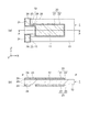
以下、本発明の実施の形態を図面に基づいて詳細に説明する。図1は、本発明の一実施形態に係る振動素子の構成を示す概略図であり、図1(a)は振動素子の平面図、図1(b)は図1(a)のP−P断面図である。 Hereinafter, embodiments of the present invention will be described in detail with reference to the drawings. FIG. 1 is a schematic diagram illustrating a configuration of a vibration element according to an embodiment of the present invention. FIG. 1 (a) is a plan view of the vibration element, and FIG. 1 (b) is a PP line of FIG. 1 (a). It is sectional drawing.
(振動素子の構成)
振動素子1は、振動部12を有する基板10と、基板10の両主面(±Y’方向の表裏面)に夫々対向するように積層された下位層の導電層としての下地電極層29と、最上位層の導電層としての電極層28と、を有している。なお、本実施形態では、二層の導電層が積層された構成で説明する。
振動素子1は、下地電極層29と電極層28とを含む励振電極20と、リード電極23と、パッド電極24と、接続電極26と、を備えている。
励振電極20は、振動部12を駆動する電極であり、振動部12の両主面(±Y’方向の表裏面)のほぼ中央部に夫々対向して形成されている。励振電極20は電極層28の一部である主電極21と下地電極層29の一部である主電極下地部22を含み、主電極21の外縁が主電極下地部22の外縁内に収まるように形成されている。
リード電極23は、励振電極20から延出されて基板10の端部に形成されたパッド電極24に導通接続されている。
パッド電極24は、基板10の両主面の端部に夫々対向して形成されている。両主面のパッド電極24は、基板10の側面部13に形成された接続電極26により導通接続されている。
(Configuration of vibration element)
The
The
The
The
The
図1(a)に示した実施形態では、振動部12のほぼ中央部の主面に夫々対向して形成された励振電極20の形状が矩形の例を示したが、これに限定する必要はなく、励振電極の形状は円形や楕円形であってもよい。
また、励振電極20、リード電極23、パッド電極24および接続電極26は、蒸着装置、或いはスパッタ装置等を用いて、例えば、下位層にクロム(Cr)を成膜し、最上位層に金(Au)を重ねて成膜してある。なお、電極材料として、下位層にクロム(Cr)の代わりにニッケル(Ni)、チタン(Ti)、ニッケルクロム合金(NiCr)、また、最上位層に金(Au)の代わりに銀(Ag)、白金(Pt)を用いても構わない。
更に、二層の導電層が積層された構成で説明したが、これに限らない。三層以上が積層された構成であってもよい。
In the embodiment shown in FIG. 1A, an example in which the shape of the
The
Furthermore, although the configuration in which two conductive layers are stacked has been described, the present invention is not limited to this. A configuration in which three or more layers are laminated may be used.
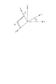
基板10が圧電材料である場合、振動素子1は、パッド電極24から入力された励振電流によって、励振電極20との間の振動部12に電界が生じ、圧電効果により振動部12が振動する。基板10を、三方晶系の圧電材料に属する水晶を用いて形成する場合、図2に示すように、互いに直交する結晶軸X,Y,Zを有する。X軸は電気軸、Y軸は機械軸、Z軸は光学軸と、夫々呼称され、XZ面をX軸の回りに所定の角度θだけ回転させた平面に沿って切り出された、所謂回転Yカット水晶基板からなる平板が基板10として用いられる。
When the
例えば、回転Yカット水晶基板がATカット水晶基板の場合、角度θは35.25°(35°15′)である。ここで、Y軸とZ軸とをX軸の回りに角度θ回転させ、Y’軸およびZ’軸とすると、ATカット水晶基板は、直交する結晶軸X,Y’,Z’を有する。従ってATカット水晶基板は、厚み方向がY’軸であり、Y’軸に直交するX軸とZ’軸を含む面が主面であり、主面に厚み滑り振動が主振動として励振される。このように形成されるATカット水晶基板から基板10が形成される。なお、本実施形態に係る基板10は、図2に示す角度θが35.25°のATカットに限定されず、例えば、厚み滑り振動を励振するBTカット等の基板10であってもよい。
For example, when the rotated Y-cut quartz substrate is an AT-cut quartz substrate, the angle θ is 35.25 ° (35 ° 15 ′). Here, when the Y-axis and the Z-axis are rotated by an angle θ around the X-axis to make the Y′-axis and the Z′-axis, the AT-cut quartz substrate has crystal axes X, Y ′, and Z ′ that are orthogonal to each other. Therefore, the AT-cut quartz substrate has a Y ′ axis in the thickness direction, a surface including the X axis and the Z ′ axis orthogonal to the Y ′ axis is a main surface, and thickness shear vibration is excited as a main vibration on the main surface. . The
(振動素子の製造方法)
次に、本発明の一実施形態に係る振動素子の製造方法について、図3のフローチャートを参照しながら説明する。振動素子1は量産性や製造コストを考慮し、大型基板から複数個の振動素子1をバッチ処理方式で製造されるのが一般的である。ここでは、一個の振動素子1の概略断面図で説明する。製造工程は、振動素子1の外形形状を形成する外形形成工程と、振動素子1の基板10の両主面に電極パターンを形成する電極形成工程と、で構成されている。
外形形成工程は、先ず、基板10を純水で洗浄し(ST11)、続いて、基板10の表裏面に、下地膜34が設けられる。これは耐食膜36となる金(Au)が基板10への付着性が弱いことを補うために設けられ、下地膜34としては、例えば、スパッタリングや蒸着等によりクロム(Cr)が成膜されている。その上には、耐食膜36として金(Au)をスパッタリング又は蒸着等により成膜する(ST12)。
次に、耐食膜36の表面全体にレジスト32を塗布し(ST13)、露光・現像することで、振動素子外形マスクを形成する(ST14)。
(Manufacturing method of vibration element)
Next, a method for manufacturing a vibration element according to an embodiment of the present invention will be described with reference to the flowchart of FIG. In consideration of mass productivity and manufacturing cost, the
In the outer shape forming step, first, the
Next, a resist 32 is applied to the entire surface of the corrosion-resistant film 36 (ST13), and exposure / development is performed to form a resonator element outer shape mask (ST14).
続いて、マスク開口から露出した耐食膜36である金(Au)を、例えば、よう化カリウム溶液を用いて、エッチングし、次いで、硝酸2セリウムアンモニウム溶液により、下地膜34であるクロム(Cr)をエッチングする(ST15)。
ここで、耐食膜36である金(Au)のエッチング液であるよう化カリウム溶液は、金(Au)を選択的にエッチングし、下地膜34であるクロム(Cr)をエッチングしない、または、エッチングしたとしてもエッチング速度は金(Au)の1/10以下である。
また、下地膜34であるクロム(Cr)のエッチング液である硝酸2セリウムアンモニウム溶液についても、クロム(Cr)を選択的にエッチングし、耐食膜36である金(Au)をエッチングしない、または、エッチングしたとしてもエッチング速度はクロム(Cr)の1/10以下である。
従って、上層の耐食膜36と下層の下地膜34とを選択的にエッチングできるため、高い寸法精度の外形マスクが形成でき、高精度の外形寸法を有する振動素子1を得ることが可能となる。
次に、マスク開口から露出した基板10を、例えば水晶基板の場合には、フッ化アンモニウム溶液等を用いてエッチングする(ST16)。これにより、図1(a)に示すように、振動素子1の外形が形成される。
続いて、レジスト32を剥離し、2種類の前記溶液を用いて耐食膜36および下地膜34を全て除去する(ST17)。
Subsequently, gold (Au), which is the corrosion-
Here, the potassium iodide solution that is an etching solution of gold (Au) that is the corrosion
Also, for the ceric ammonium nitrate solution that is an etching solution of chromium (Cr) that is the
Accordingly, since the upper corrosion-
Next, the
Subsequently, the resist 32 is peeled off, and the corrosion-
次に、電極形成工程を説明する。電極形成についても外形形成と同様に、基板10の表裏面に、最上位層の導電層としての電極層28である金(Au)と基板10の付着性を高めるためのクロム(Cr)を下位層の導電層としての下地電極層29とを、クロム(Cr)、金(Au)の順番でスパッタリング又は蒸着等により成膜する(ST18)。
次に、電極層28の表面全体にレジスト32を塗布し(ST19)、露光・現像することで、励振電極マスクを形成する(ST20)。
続いて、励振電極20用の金(Au)、クロム(Cr)のエッチングも外形形成工程で用いた溶液でエッチングする。先ず、電極層28となる金(Au)をエッチングし(ST21)、その後、下地電極層29のクロム(Cr)をエッチングする(ST22)。この時に、電極層28と基板10との間に空隙部70が生じてしまうので、次に、この空隙部70を除去するために、再び電極層28となる金(Au)をエッチングする(ST23)。
ここで、電極層28と下地電極層29とを選択的にエッチングできるエッチング液を用いているため、高精度の外形寸法を有する振動素子が得られるのと同様に、高精度の外形寸法を有する励振電極20を得ることが可能である。
その後、レジスト32を剥離し(ST24)、振動素子1を完成させている。
Next, an electrode formation process will be described. In the electrode formation, as in the outer shape formation, gold (Au), which is the
Next, a resist 32 is applied to the entire surface of the electrode layer 28 (ST19), and exposed and developed to form an excitation electrode mask (ST20).
Subsequently, gold (Au) and chromium (Cr) for the
Here, since an etching solution capable of selectively etching the
Thereafter, the resist 32 is peeled off (ST24), and the
従来の製造方法では、下地電極層29のクロム(Cr)をエッチングした後、レジスト32を剥離し(ST24に相当する)、振動素子1を完成させていた。そのため、電極層28と基板10との間に空隙部70を有した振動素子1であった。
上述した実施形態の製造方法では、下地電極層29のクロム(Cr)のエッチング(ST22)後に、再び電極層28となる金(Au)をエッチングする(ST23)。
これにより、下地電極層29のクロム(Cr)をエッチングした後に、電極層28と基板10との間に生じる空隙部70をなくすことができる。この空隙部70がなくなることについて次に説明する。
In the conventional manufacturing method, after etching chromium (Cr) of the
In the manufacturing method of the above-described embodiment, after the chromium (Cr) etching of the base electrode layer 29 (ST22), the gold (Au) that becomes the
Thereby, after the chromium (Cr) of the
図4は本発明の一実施形態に係る振動素子の電極の構成を説明する拡大断面図であり、図4(a)は本実施形態に係る製造方法により製造した振動素子の断面図、図4(b)は従来の製造方法により製造した振動素子の断面図である。
図4(b)に示す従来の如き製造方法により製造された振動素子200では、主電極221と基板210との間に空隙部270があるのに対し、図4(a)の本実施形態に係る製造方法における振動素子1では、図3(ST22)に示す空隙部70が生じていない。従来の製造方法で主電極221と基板210との間に空隙部270が生じる要因は、成膜した金属材料が等方性であり、エッチングの際に基板面に垂直な方向だけでなく、基板に平行な方向にもエッチングが進行することにより主電極下地部222の側壁面もエッチングが進行してしまうという現象であるサイドエッチングやエッチング液がマスクの下に回り込んだ腐食現象であるアンダーカットが起こるためである。従って、下地電極層29の一部である主電極下地部222はクロム(Cr)エッチングにおいて、マスクとなる主電極221よりも外形形状(外縁)が小さくなり空隙部270を生じる。この空隙部270がDLD特性を非常に悪くし、製造歩留りを著しく低下させていることが本願発明者らの研究や実験と解析により判明した。
FIG. 4 is an enlarged cross-sectional view illustrating the configuration of the electrodes of the vibration element according to the embodiment of the present invention. FIG. 4A is a cross-sectional view of the vibration element manufactured by the manufacturing method according to the embodiment. (B) is sectional drawing of the vibration element manufactured by the conventional manufacturing method.
In the
そのため、本実施形態に係る製造方法では、主電極下地部22のクロム(Cr)エッチング(図3に示すST22)後に、空隙部70により主電極下地部22の外形よりも外側へ突出した領域の主電極21である金(Au)を再度エッチングする(図3に示すST23)工程を追加した。この再度エッチング(ST23)により、少なくとも前記突出した領域の金(Au)が除去されることによって、空隙部70がなくなる。これにより、主電極21の外縁が主電極下地部22の外縁よりも内側に収まるようになり、主電極21と主電極下地部22との界面の全域において、主電極21が主電極下地部22に密着した励振電極20を形成することを実現した。
なお、ここでは図1に示す励振電極20を例に説明したが他の電極(リード電極23、パッド電極24、接続電極26)においても同様な電極構成とすることが好ましい。
Therefore, in the manufacturing method according to the present embodiment, after the chromium (Cr) etching of the main electrode base portion 22 (ST22 shown in FIG. 3), the region protruding outside from the outer shape of the main
Here, although the
図5は本発明の一実施形態に係る製造方法により製造した振動素子のDLD特性であり、図5(a)は周波数変化量、図5(b)はCI変化量である。
また、図6は従来の製造方法により製造した振動素子のDLD特性であり、図6(a)は周波数変化量、図6(b)はCI変化量である。
図5と図6より、本実施形態に係る製造方法による振動素子1のDLD特性は、従来の製造方法のものに比べ、周波数とCI共にばらつきが小さく、安定している。
これまで、DLD特性の劣化は、振動素子1の加工時に起こる基板への残留応力や汚染等の発生が原因と言われていた。残留応力については、フォトリソ技術による外形加工を施しているためその影響は極力小さいものと考えられ、汚染についてもクリーンルーム内での作業や組み立て時にオーバードライブ(強励振駆動)により金属膜片や基板片を除去する工程を行っていることから影響は小さいものと考えられる。
しかし、従来の如き製造方法により製造された振動素子200のDLD特性が大きくばらつく要因は、主電極221と基板210との間に生じた空隙部270による影響が大きいことが本願発明者らの研究によって明らかとなってきた。つまり、主電極下地部222が除去されてしまった空隙部270周辺の主電極221の一部があたかも金属片、金属粉などの異物が付着した状態と同様な状態となり、励振時に振動エネルギーを漏洩し、周波数変化やCI変化を生じさせたものと考えられる。
従って、主電極下地部22のクロム(Cr)をエッチング(ST22)後に、再び主電極21となる金(Au)をエッチングする(ST23)工程を追加した本実施形態に係る製造方法は、DLD特性を劣化すると予想される主電極下地部22と密着しない主電極21を生じさせないので、振動素子1のDLD特性検査の歩留りを向上させ、DLD特性の非常に優れた振動素子を製造できるという非常に大きな効果を発揮する。
5A and 5B show DLD characteristics of the resonator element manufactured by the manufacturing method according to the embodiment of the present invention. FIG. 5A shows the frequency change amount and FIG. 5B shows the CI change amount.
FIG. 6 shows the DLD characteristics of the vibration element manufactured by the conventional manufacturing method. FIG. 6A shows the frequency change amount, and FIG. 6B shows the CI change amount.
5 and 6, the DLD characteristics of the
Until now, it has been said that the deterioration of the DLD characteristics is caused by the occurrence of residual stress or contamination on the substrate that occurs during processing of the
However, the present inventors have studied that the cause of the large variation in the DLD characteristics of the
Therefore, the manufacturing method according to the present embodiment in which the step of etching gold (Au) to be the
図7は、本発明の一実施形態に係る振動素子の構成を示す概略図であり、図7(a)は振動素子の平面図、図7(b)は図1(a)のP−P断面図である。
振動素子2は、振動部12を有する基板10と、基板10の両主面(±Y’方向の表裏面)に夫々対向するように積層された下位層の導電層としての下地電極層29と、最上位層の導電層としての電極層28と、を有している。
振動素子2は、基板10と、下地電極層29と電極層28とを含む励振電極20と、リード電極23と、パッド電極24と、接続電極26と、を備えている。
基板10は、振動部12と、振動部12より板厚の薄い薄肉部14と、を備えている。
励振電極20は、振動部12を駆動する電極であり、振動部12の両主面(±Y’方向の表裏面)のほぼ中央部に夫々対向して形成されている。励振電極20は電極層28の一部である主電極21と下地電極層29の一部である主電極下地部22を含み、主電極21の外縁が主電極下地部22の外縁内に収まるように形成されている。
リード電極23は、励振電極20から延出されて基板10の端部に形成されたパッド電極24に導通接続されている。
パッド電極24は、基板10の薄肉部14の両主面の端部に夫々対向して形成されている。両主面のパッド電極24は、基板10の側面部13に形成された接続電極26により導通接続されている。
7A and 7B are schematic diagrams illustrating a configuration of a vibration element according to an embodiment of the present invention. FIG. 7A is a plan view of the vibration element, and FIG. 7B is a PP line in FIG. It is sectional drawing.
The
The
The
The
The
The
図7(a)に示した実施形態では、振動部12のほぼ中央部の主面に夫々対向して形成された励振電極20の形状が矩形の例を示したが、これに限定する必要はなく、励振電極20の形状は円形や楕円形であってもよい。
また、基板10の表裏両主面に段差が1段のメサ部16の例を示したが、これに限定する必要はなく、基板10の表裏両主面に多段のメサ形状や基板10の表または裏の主面のどちらか一方に1段から多段のメサ形状を有していてもよい。更に、メサ部16の形状が矩形の例を示したが、これに限定する必要はなく、メサ部16の形状も円形や楕円形であってもよい。
図7に示すように、振動部12にメサ部16を有するメサ構造の基板10とすると、輪郭系スプリアスとの結合を回避し、主振動のみの振動エネルギーを閉じ込めることができるため、CIが小さく、共振周波数近傍のスプリアスを抑制した小型の振動素子2が得られるという効果がある。
In the embodiment shown in FIG. 7A, an example is shown in which the shape of the
In addition, the example of the
As shown in FIG. 7, when the
図8は、本発明の一実施形態に係る振動素子の別の構造を示す概略図であり、図8(a)は変形例1の平面図、図8(b)は変形例2の平面図、図8(c)は変形例3の平面図である。
図8(a)は図7に示す本実施の形態の第1の変形例を示したものであり、基板10の表裏両主面に形成された励振電極20とメサ部16のX軸方向とZ’軸方向の長さがともにメサ部16に比べ励振電極20の方が長い場合である。図8(b)は第2の変形例であり、励振電極20とメサ部16のZ’軸方向の長さがほぼ同等で、X軸方向の長さは励振電極20が長い場合である。図8(c)は第3の変形例であり、励振電極20とメサ部16のX軸方向の長さがほぼ同等で、Z’軸方向の長さは励振電極20が長い場合である。
図8(a)〜図8(c)は図7に比べ、励振電極20の面積が大きくすることができるため、振動子の容量比を小さくすることができる。そのため、発振器に用いた場合、周波数調整量や周波数可変量を拡大することができるという効果がある。
8A and 8B are schematic views showing another structure of the resonator element according to the embodiment of the invention. FIG. 8A is a plan view of the first modification, and FIG. 8B is a plan view of the second modification. FIG. 8C is a plan view of the third modification.
FIG. 8A shows a first modification of the present embodiment shown in FIG. 7, in which the
8A to 8C, the area of the
図9は、本発明の一実施形態に係る振動素子の変形例4の構造を示す概略図であり、図9(a)は振動素子の平面図、図9(b)は図9(a)のP−P断面図である。
振動素子3は、振動部12を有する基板10と、基板10の両主面(±Y’方向の表裏面)に夫々対向するように積層された下位層の導電層としての下地電極層29と、最上位層の導電層としての電極層28と、を有している。
振動素子3は、基板10と、下地電極層29と電極層28とを含む励振電極20と、リード電極23と、パッド電極24と、接続電極26と、を備えている。
基板10は、振動部12と、振動部12より板厚の厚い厚肉部15と、を備えている。
励振電極20は、振動部12を駆動する電極であり、振動部12の両主面(±Y’方向の表裏面)のほぼ中央部に夫々対向して形成されている。励振電極20は電極層28の一部である主電極21と下地電極層29の一部である主電極下地部22を含み、主電極21の外縁が主電極下地部22の外縁内に収まるように形成されている。
リード電極23は、励振電極20から延出されて基板10の端部に形成されたパッド電極24に導通接続されている。
パッド電極24は、基板10の厚肉部15の両主面の端部に夫々対向して形成されている。両主面のパッド電極24は、基板10の側面部13に形成された接続電極26により導通接続されている。
FIG. 9 is a schematic view showing the structure of a
The
The
The
The
The
The
図9(a)に示した実施形態では、振動部12のほぼ中央部の主面に夫々対向して形成された励振電極20の形状と面積が同一の矩形の例を示したが、これに限定する必要はなく、励振電極20の形状と面積が上下で異なり、形状も円形や楕円形であってもよい。
また、基板10のほぼ中央に形成された凹陥部17は、基板10の片面からエッチングにより形成されているが、基板10の両面からエッチングを施し、夫々対向して凹陥部17を形成してもよい。
図9に示すように、凹陥部17を振動部12とする逆メサ構造の基板10とすることで、振動部12を非常に薄くできるため共振周波数の高周波化が可能となり、また、振動部12と一体化された厚肉部15でマウントすることができるので、耐衝撃性や耐振動性に優れた高信頼性で高周波の振動素子3が得られるという効果がある。
In the embodiment shown in FIG. 9A, an example of a rectangular shape having the same shape and area of the
In addition, the
As shown in FIG. 9, by using a
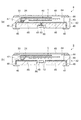
図10は本発明の一実施形態に係る振動子の構成を示す概略図であり、図10(a)は蓋部材を省略した平面図であり、図10(b)は縦断面図である。振動子5は、振動素子1と、振動素子1を収容するために矩形の箱状に形成されているパッケージ本体40と、金属、セラミック、ガラス等から成る蓋部材49と、等で構成されている。
パッケージ本体40は、図10に示すように、第1の基板41と、第2の基板42と、第3の基板43と、シールリング44と、実装端子45と、を積層して形成されている。実装端子45は、第1の基板41の外部底面に複数形成されている。第3の基板43は中央部が除去された環状体であり、第3の基板43の上部周縁に例えばコバール等のシールリング44が形成されている。
第3の基板43と第2の基板42とにより、振動素子1を収容するキャビティー84が形成される。第2の基板42の上面の所定の位置には、導体46により実装端子45と電気的に導通する複数の素子搭載パッド47が設けられている。素子搭載パッド47は、振動素子1を載置した際に基板10の端部に形成したパッド電極24に対応するように配置されている。
FIG. 10 is a schematic view showing a configuration of a vibrator according to an embodiment of the present invention, FIG. 10 (a) is a plan view in which a lid member is omitted, and FIG. 10 (b) is a longitudinal sectional view. The
As shown in FIG. 10, the
The
振動素子1を支持固定する際には、先ず、振動素子1のパッド電極24を導電性接着剤30が塗布された素子搭載パッド47に載置して荷重をかける。
次に、導電性接着剤30を硬化させるために、所定の温度の高温炉に所定の時間入れる。導電性接着剤30を硬化させた後、アニール処理を施し、励振電極20に質量を付加するか、又は質量を減じて周波数調整を行う。その後、パッケージ本体40の第3の基板43の上面に形成したシールリング44上に、蓋部材49を載置し、真空中、又は窒素ガスの雰囲気中で蓋部材49をシーム溶接して密封し、振動子5が完成する。
又は、パッケージ本体40の上面に塗布した低融点ガラスに蓋部材49を載置し、溶融して密着する方法もある。この場合もパッケージのキャビティ内は真空にするか、又は窒素ガス等の不活性ガスで充填して、振動子5が完成する。
以上の振動子5の実施形態では、パッケージ本体40に積層板を用いた例を説明したが、パッケージ本体40に単層セラミック板を用い、蓋体に絞り加工を施したキャップを用いて振動子5を構成してもよい。
When the
Next, in order to cure the
Alternatively, there is also a method in which the
In the above-described embodiment of the
図11は本発明の一実施形態に係る電子デバイスの構成を示す概略図であって、図11(a)は蓋部材を省略した平面図であり、図11(b)は縦断面図である。
電子デバイス7は、パッケージ本体50と、蓋部材49と、振動素子1と、振動素子1を励振する発振回路を搭載したIC部品51と、電圧により容量が変化する可変容量素子、温度により抵抗が変化するサーミスター、インダクター等の電子部品52の少なくとも1つと、を備えている。
パッケージ本体50は、図11に示すように、第1の基板61と、第2の基板62と、第3の基板63と、を積層して形成されている。実装端子45は、第1の基板61の外部底面に複数形成されている。第2の基板62と第3の基板63とは中央部が除去された環状体で形成されている。
第1の基板61と、第2の基板62と、第3の基板63と、により、振動素子1、IC部品51、および電子部品52等を収容するキャビティー84が形成される。第2の基板62の上面の所定の位置には、導体46により実装端子45と電気的に導通する複数の素子搭載パッド47が設けられている。素子搭載パッド47の位置は、振動素子1を載置した際に基板10の端部に形成したパッド電極24に対応するように配置されている。
FIG. 11 is a schematic view showing a configuration of an electronic device according to an embodiment of the present invention. FIG. 11 (a) is a plan view in which a lid member is omitted, and FIG. 11 (b) is a longitudinal sectional view. .
The
As shown in FIG. 11, the package
The
振動素子1のパッド電極24を、導電性接着剤30を塗布したパッケージ本体50の素子搭載パッド47に載置し、所定の温度で導電性接着剤30を硬化させることで、パッド電極24と素子搭載パッド47との導通を図る。IC部品51をパッケージ本体50の所定の位置に固定し、IC部品51の端子と、パッケージ本体50の電極端子55とをボンディングワイヤーBWにて接続する。また、電子部品52は、パッケージ本体50の所定の位置に載置し、金属バンプ等を用いて導体46に接続する。パッケージ本体50を真空、或いは窒素等の不活性気体で満たし、パッケージ本体50を蓋部材49で密封して電子デバイス7を完成する。
図11に示すように、DLD特性の良好な振動素子1を用いているので、起動特性に優れた小型の電子デバイス7が得られる。
また、電子デバイス7として、小型の発振器、温度補償型発振器、電圧制御型発振器等を構成することができる。
The
As shown in FIG. 11, since the
As the
次に、本実施形態に係る別の電子デバイスについて、図面を参照しながら説明する。
図12(a)は、図11の変形例の電子デバイス8の断面図である。電子デバイス8は、本発明の振動素子1と、感温素子であるサーミスター53と、振動素子1およびサーミスター53を収容するパッケージ82と、を概略備えている。パッケージ82は、パッケージ本体80と、蓋部材49とを備えている。パッケージ本体80は、上面側に振動素子1を収容するキャビティー84が形成され、下面側にサーミスター53を収容する凹部86が形成されている。キャビティー84の内底面の端部に複数の素子搭載パッド47が設けられ、各素子搭載パッド47は導体46で複数の実装端子45と導通接続されている。素子搭載パッド47に導電性接着剤30を塗布し、この導電性接着剤30の上に振動素子1を載置して、パッド電極24と、各素子搭載パッド47とを導電性接着剤30を介して電気的に接続し、固定する。パッケージ本体80の上部には、シールリング44が焼成されており、このシールリング44に蓋部材49を載置し、抵抗溶接機を用いて溶接し、キャビティー84を気密封止する。キャビティー84内は真空にしてもよいし、不活性ガスを封入してもよい。
一方、パッケージ本体80の下面側略中央には凹部86が形成され、凹部86の上面には電子部品搭載パッド48が焼成されている。電子部品搭載パッド48にサーミスター53を搭載し、半田等を用いて導通接続して電子デバイス8を構成する。なお、電子部品搭載パッド48は、導体46で複数の実装端子45と導通接続されている。
Next, another electronic device according to the present embodiment will be described with reference to the drawings.
FIG. 12A is a cross-sectional view of an electronic device 8 according to a modification of FIG. The electronic device 8 roughly includes the
On the other hand, a
図12(b)は、図12(a)の変形例の電子デバイス9であって、電子デバイス8と異なる点は、パッケージ本体80のキャビティー84の底面に凹部86が形成されており、この凹部86の底面に焼成された電子部品搭載パッド48に、金属バンプ等を介してサーミスター53が接続されている所である。電子部品搭載パッド48は実装端子45と導通されている。つまり、振動素子1と感温素子のサーミスター53とが、キャビティー84内に収容され、気密封止されている。
以上では、振動素子1とサーミスター53とをパッケージ82に収容した例を説明したが、パッケージ82に収容する電子部品としては、サーミスター、コンデンサー、リアクタンス素子、半導体素子のうち少なくとも一つを収容した電子デバイス9を構成することが望ましい。
上記のように振動素子を製作できるので電子デバイスの納期を大幅に短縮することが可能となる。また、上記の振動素子と、サーミスター、コンデンサー、リアクタンス素子、半導体素子等を組み合わせることにより、多様な仕様の要求に素早く対応できるという効果がある。
FIG. 12B shows an electronic device 9 according to a modification of FIG. 12A, which is different from the electronic device 8 in that a
The example in which the
Since the vibration element can be manufactured as described above, the delivery time of the electronic device can be greatly shortened. Further, by combining the vibration element with the thermistor, the capacitor, the reactance element, the semiconductor element, etc., there is an effect that it is possible to quickly meet the requirements of various specifications.
次いで、本発明の一実施形態に係る振動素子を適用した電子機器(本発明の電子機器)について、図13〜図15に基づき、詳細に説明する。
図13は、本発明の一実施形態に係る振動素子を備える電子機器としてのモバイル型(又はノート型)のパーソナルコンピューターの構成を示す斜視図である。この図において、パーソナルコンピューター1100は、キーボード1102を備えた本体部1104と、表示部100を備えた表示ユニット1106とにより構成され、表示ユニット1106は、本体部1104に対しヒンジ構造部を介して回動可能に支持されている。このようなパーソナルコンピューター1100には、フィルター、共振器、基準クロック等の少なくとも一つとして機能する振動素子1が内蔵されている。
Next, an electronic device (an electronic device of the present invention) to which the vibration element according to an embodiment of the present invention is applied will be described in detail with reference to FIGS.
FIG. 13 is a perspective view illustrating a configuration of a mobile (or notebook) personal computer as an electronic apparatus including the resonator element according to the embodiment of the invention. In this figure, a
図14は、本発明の一実施形態に係る振動素子を備える電子機器としての携帯電話機(PHSも含む)の構成を示す斜視図である。この図において、携帯電話機1200は、複数の操作ボタン1202、受話口1204および送話口1206を備え、操作ボタン1202と受話口1204との間には、表示部100が配置されている。このような携帯電話機1200には、フィルター、共振器等として機能する振動素子1が内蔵されている。
FIG. 14 is a perspective view illustrating a configuration of a mobile phone (including PHS) as an electronic apparatus including the resonator element according to the embodiment of the invention. In this figure, a
図15は、本発明の一実施形態に係る振動素子を備える電子機器としてのデジタルカメラの構成を示す斜視図である。なお、この図には、外部機器との接続についても簡易的に示されている。ここで、通常のカメラは、被写体の光像により銀塩写真フィルムを感光するのに対し、デジタルカメラ1300は、被写体の光像をCCD(Charge Coupled Device)等の撮像素子により光電変換して撮像信号(画像信号)を生成する。
デジタルカメラ1300におけるケース(ボディー)1302の背面には、表示部100が設けられ、CCDによる撮像信号に基づいて表示を行う構成になっており、表示部100は、被写体を電子画像として表示するファインダーとして機能する。また、ケース1302の正面側(図中裏面側)には、光学レンズ(撮像光学系)やCCD等を含む受光ユニット1304が設けられている。
撮影者が表示部100に表示された被写体像を確認し、シャッターボタン1306を押下すると、その時点におけるCCDの撮像信号が、メモリー1308に転送・格納される。また、このデジタルカメラ1300においては、ケース1302の側面に、ビデオ信号出力端子1312と、データ通信用の入出力端子1314とが設けられている。そして、図示されるように、ビデオ信号出力端子1312にはテレビモニター1430が、データ通信用の入出力端子1314にはパーソナルコンピューター1440が、夫々必要に応じて接続される。さらに、所定の操作により、メモリー1308に格納された撮像信号が、テレビモニター1430や、パーソナルコンピューター1440に出力される構成になっている。このようなデジタルカメラ1300には、フィルター、共振器等として機能する振動素子1が内蔵されている。
FIG. 15 is a perspective view illustrating a configuration of a digital camera as an electronic apparatus including the vibration element according to the embodiment of the invention. In this figure, connection with an external device is also simply shown. Here, a normal camera sensitizes a silver salt photographic film with a light image of a subject, whereas a
A
When the photographer confirms the subject image displayed on the
なお、本発明の一実施形態に係る振動素子を備える電子機器は、図13のパーソナルコンピューター(モバイル型パーソナルコンピューター)、図14の携帯電話機、図15のデジタルカメラの他にも、例えば、インクジェット式吐出装置(例えばインクジェットプリンター)、ラップトップ型パーソナルコンピューター、テレビ、ビデオカメラ、ビデオテープレコーダー、カーナビゲーション装置、ページャー、電子手帳(通信機能付も含む)、電子辞書、電卓、電子ゲーム機器、ワードプロセッサー、ワークステーション、テレビ電話、防犯用テレビモニター、電子双眼鏡、POS端末、医療機器(例えば電子体温計、血圧計、血糖計、心電図計測装置、超音波診断装置、電子内視鏡)、魚群探知機、各種測定機器、計器類(例えば、車両、航空機、船舶の計器類)、フライトシミュレーター等に適用することができる。 Note that the electronic apparatus including the resonator element according to the embodiment of the invention includes, for example, an ink jet type in addition to the personal computer (mobile personal computer) in FIG. 13, the mobile phone in FIG. 14, and the digital camera in FIG. 15. Discharge device (for example, inkjet printer), laptop personal computer, TV, video camera, video tape recorder, car navigation device, pager, electronic notebook (including communication function), electronic dictionary, calculator, electronic game device, word processor, Workstations, videophones, crime prevention TV monitors, electronic binoculars, POS terminals, medical equipment (for example, electronic thermometers, blood pressure monitors, blood glucose meters, electrocardiogram measuring devices, ultrasonic diagnostic devices, electronic endoscopes), fish detectors, various types Measuring equipment, instruments (eg cars , Aircraft, gauges of a ship), can be applied to a flight simulator or the like.
図16は移動体の一具体例としての自動車106を概略的に示す。自動車106には本発明に係る振動素子を有する振動子や電子デバイスが搭載されている。
例えば、キーレスエントリー、イモビライザー、カーナビゲーションシステム、カーエアコン、アンチロックブレーキシステム(ABS:Antilock Brake System)、エアバック、タイヤプレッシャーモニタリングシステム(TPMS:Tire Pressure Monitoring System)、エンジンコントロール、ハイブリッド自動車や電気自動車の電池モニター、車体姿勢制御システム、等の電子制御ユニット(ECU:electronic control unit)108に広く適用できる。
FIG. 16 schematically shows an
For example, keyless entry, immobilizer, car navigation system, car air conditioner, antilock brake system (ABS), airbag, tire pressure monitoring system (TPMS), engine control, hybrid car and electric car The present invention can be widely applied to electronic control units (ECUs) 108 such as battery monitors and vehicle attitude control systems.
1,2,3,101,102,103,200…振動素子、5…振動子、7,8,9…電子デバイス、10,210…基板、12,212…振動部、13…側面部、14…薄肉部、15…厚肉部、16…メサ部、17…凹陥部、20…励振電極、21,221…主電極、22,222…主電極下地部、23…リード電極、24…パッド電極、26…接続電極、28…電極層、29…下地電極層、30…導電性接着剤、32…レジスト、34…下地膜、36…耐食膜、40,50,80…パッケージ本体、41…第1の基板、42…第2の基板、43…第3の基板、44…シールリング、45…実装端子、46…導体、47…素子搭載パッド、48…電子部品搭載パッド、49…蓋部材、50…パッケージ本体、51…IC部品、52…電子部品、53…サーミスター、55…電極端子、61…第1の基板、62…第2の基板、63…第3の基板、70,270…空隙部、82…パッケージ、84…キャビティー、86…凹部、100…表示部、106…自動車、107…車体、108…電子制御ユニット、109…タイヤ、1100…パーソナルコンピューター、1102…キーボード、1104…本体部、1106…表示ユニット、1200…携帯電話機、1202…操作ボタン、1204…受話口、1206…送話口、1300…デジタルカメラ、1302…ケース、1304…受光ユニット、1306…シャッターボタン、1308…メモリー、1312…ビデオ信号出力端子、1314…入出力端子、1430…テレビモニター、1440…パーソナルコンピューター。
1, 2, 3, 101, 102, 103, 200 ... vibration element, 5 ... vibrator, 7, 8, 9 ... electronic device, 10, 210 ... substrate, 12, 212 ... vibration part, 13 ... side part, 14 ... Thin part, 15 ... Thick part, 16 ... Mesa part, 17 ... Recessed part, 20 ... Excitation electrode, 21 221 ... Main electrode, 22, 222 ... Main electrode base part, 23 ... Lead electrode, 24 ... Pad electrode , 26 ... connection electrode, 28 ... electrode layer, 29 ... base electrode layer, 30 ... conductive adhesive, 32 ... resist, 34 ... base film, 36 ... corrosion resistant film, 40, 50, 80 ... package body, 41 ... first 1
Claims (4)
積層されている前記導電層の内の上層の導電層をエッチング加工する工程と、
前記導電層の面積が前記振動部の面積よりも大きくなるように、前記上層の導電層よりも前記基板側に設けられている下層の導電層をエッチング加工する工程と、
前記上層の導電層を、前記下層の導電層よりも前記上層の導電層に対してエッチング速度が大きいエッチング液でエッチング加工する工程と、
を含むことを特徴とする振動素子の製造方法。 A step of preparing a substrate on which two or more conductive layers of different materials are laminated, comprising a vibrating portion that vibrates in thickness and an outer edge portion that is disposed around the vibrating portion and is thinner than the thickness of the vibrating portion;
Etching the upper conductive layer of the stacked conductive layers; and
Etching the lower conductive layer provided on the substrate side of the upper conductive layer so that the area of the conductive layer is larger than the area of the vibrating portion;
The conductive layer of the upper layer, the step of etching the etching rate is large etching grayed liquid to the conductive layer of the upper layer than the lower conductive layer,
The manufacturing method of the vibration element characterized by including this.
前記上層の導電層をエッチング加工する工程で使用されるエッチング液に対して、前記下層の導電層のエッチング速度は、前記上層の導電層のエッチング速度よりも遅く、
前記下層の導電層をエッチング加工する工程で使用されるエッチング液に対して、前記上層の導電層のエッチング速度は、前記下層の導電層のエッチング速度よりも遅いことを特徴とする振動素子の製造方法。 In claim 1 ,
For the etchant used in the step of etching the upper conductive layer, the etching rate of the lower conductive layer is slower than the etching rate of the upper conductive layer,
Manufacturing of a vibrating element, wherein an etching rate of the upper conductive layer is lower than an etching rate of the lower conductive layer with respect to an etching solution used in the step of etching the lower conductive layer Method.
前記上層の導電層と前記下層の導電層は材料が異なることを特徴とする振動素子の製造方法。 In claim 1 or claim 2 ,
The method for manufacturing a vibration element, wherein the upper conductive layer and the lower conductive layer are made of different materials.
前記上層の導電層の材料が、Au、Ag、及びPtのいずれかであり、
前記下層の導電層の材料が、Cr、Ni、Ti、及びNiCr合金のいずれかであることを特徴とする振動素子の製造方法。 In claim 3 ,
The material of the upper conductive layer is any one of Au, Ag, and Pt,
Method for manufacturing a vibrating element material of the lower conductive layer is Cr, Ni, Ti, and wherein a is any one of NiCr alloy.
Priority Applications (8)
| Application Number | Priority Date | Filing Date | Title |
|---|---|---|---|
| JP2012128662A JP6175743B2 (en) | 2012-06-06 | 2012-06-06 | Manufacturing method of vibration element |
| US13/910,569 US9450166B2 (en) | 2012-06-06 | 2013-06-05 | Resonator element, resonator, electronic device, electronic apparatus, mobile body and method of manufacturing resonator element |
| CN201310221542.7A CN103475328B (en) | 2012-06-06 | 2013-06-05 | Vibrating elements and its manufacturing method, oscillator, electronic device and equipment, moving body |
| CN201320322501.2U CN203377847U (en) | 2012-06-06 | 2013-06-05 | Vibration element, vibrator, electronic device, electronic equipment and mobile body |
| CN201910001026.0A CN110011630B (en) | 2012-06-06 | 2013-06-05 | Vibrating element, vibrator, electronic device, electronic apparatus, and moving object |
| US15/165,090 US10147867B2 (en) | 2012-06-06 | 2016-05-26 | Resonator element, resonator, electronic device, electronic apparatus, mobile body and method of manufacturing resonator element |
| US16/176,552 US10680158B2 (en) | 2012-06-06 | 2018-10-31 | Resonator element, resonator, electronic device, electronic apparatus, mobile body and method of manufacturing resonator element |
| US16/860,101 US11495727B2 (en) | 2012-06-06 | 2020-04-28 | Resonator element, resonator, electronic device, electronic apparatus, mobile body and method of manufacturing resonator element |
Applications Claiming Priority (1)
| Application Number | Priority Date | Filing Date | Title |
|---|---|---|---|
| JP2012128662A JP6175743B2 (en) | 2012-06-06 | 2012-06-06 | Manufacturing method of vibration element |
Related Child Applications (1)
| Application Number | Title | Priority Date | Filing Date |
|---|---|---|---|
| JP2017008270A Division JP6315115B2 (en) | 2017-01-20 | 2017-01-20 | Vibration element, vibrator, electronic device, electronic device, and moving object |
Publications (3)
| Publication Number | Publication Date |
|---|---|
| JP2013255052A JP2013255052A (en) | 2013-12-19 |
| JP2013255052A5 JP2013255052A5 (en) | 2015-07-09 |
| JP6175743B2 true JP6175743B2 (en) | 2017-08-09 |
Family
ID=49714714
Family Applications (1)
| Application Number | Title | Priority Date | Filing Date |
|---|---|---|---|
| JP2012128662A Expired - Fee Related JP6175743B2 (en) | 2012-06-06 | 2012-06-06 | Manufacturing method of vibration element |
Country Status (3)
| Country | Link |
|---|---|
| US (4) | US9450166B2 (en) |
| JP (1) | JP6175743B2 (en) |
| CN (3) | CN103475328B (en) |
Families Citing this family (19)
| Publication number | Priority date | Publication date | Assignee | Title |
|---|---|---|---|---|
| CN202535316U (en) | 2011-03-09 | 2012-11-14 | 精工爱普生株式会社 | Vibrating element, vibrator, oscillator and electronic equipment |
| JP5708089B2 (en) | 2011-03-18 | 2015-04-30 | セイコーエプソン株式会社 | Piezoelectric vibration element, piezoelectric vibrator, piezoelectric oscillator, and electronic device |
| JP6644457B2 (en) * | 2014-03-26 | 2020-02-12 | Tdk株式会社 | Piezo device |
| JP2015211362A (en) * | 2014-04-28 | 2015-11-24 | 京セラクリスタルデバイス株式会社 | Quarts device and manufacturing method for quarts device |
| JP6618675B2 (en) | 2014-07-30 | 2019-12-11 | セイコーエプソン株式会社 | Vibrating device, electronic device, and moving object |
| JP6390836B2 (en) | 2014-07-31 | 2018-09-19 | セイコーエプソン株式会社 | Vibrating piece, vibrator, vibrating device, oscillator, electronic device, and moving object |
| JP6738588B2 (en) * | 2014-09-02 | 2020-08-12 | セイコーエプソン株式会社 | Oscillators, electronics, and mobiles |
| JP2016127467A (en) * | 2015-01-06 | 2016-07-11 | セイコーエプソン株式会社 | Vibration device, electronic apparatus and mobile object |
| JP2016140024A (en) | 2015-01-29 | 2016-08-04 | セイコーエプソン株式会社 | Vibrating piece, vibrator, oscillation device, oscillator and mobile object |
| JP2017192032A (en) * | 2016-04-13 | 2017-10-19 | 日本電波工業株式会社 | Crystal resonator |
| US10367510B2 (en) * | 2016-05-13 | 2019-07-30 | Nihon Dempa Kogyo Co., Ltd. | Crystal oscillator and method for manufacturing crystal oscillator |
| JP2017208798A (en) * | 2016-05-13 | 2017-11-24 | 日本電波工業株式会社 | Crystal oscillator and method of manufacturing crystal oscillator |
| JP2018164126A (en) | 2017-03-24 | 2018-10-18 | セイコーエプソン株式会社 | Vibration device, generator, gyro sensor, electronic apparatus and moving body |
| CN108392200B (en) * | 2017-12-29 | 2021-10-29 | 深圳市亮动科技开发有限公司 | Electrode component of electrocardio monitoring equipment and electrocardio monitoring equipment thereof |
| JP7311152B2 (en) * | 2020-03-18 | 2023-07-19 | 有限会社マクシス・ワン | Crystal oscillator electrode structure, crystal oscillator, crystal oscillator |
| CN117769803A (en) * | 2021-09-24 | 2024-03-26 | 株式会社大真空 | Piezoelectric vibration device |
| WO2023085238A1 (en) * | 2021-11-09 | 2023-05-19 | 株式会社大真空 | Crystal oscillation device with thermistor |
| WO2023085348A1 (en) * | 2021-11-15 | 2023-05-19 | 京セラ株式会社 | Crystal element and crystal device |
| FI20225530A1 (en) * | 2022-06-14 | 2023-12-15 | Teknologian Tutkimuskeskus Vtt Oy | Acoustic wave resonator |
Family Cites Families (49)
| Publication number | Priority date | Publication date | Assignee | Title |
|---|---|---|---|---|
| JPS5728415A (en) * | 1980-07-29 | 1982-02-16 | Citizen Watch Co Ltd | Electrode film construction of quartz oscillator |
| JPS5751331U (en) * | 1980-09-09 | 1982-03-24 | ||
| JPS5751331A (en) | 1980-09-12 | 1982-03-26 | Zenitakagumi:Kk | Construction of continuous underground wall |
| JPS5925831A (en) * | 1982-08-03 | 1984-02-09 | Showa Denko Kk | Automobile flexible booth |
| JPH02260910A (en) | 1989-03-31 | 1990-10-23 | Meidensha Corp | Crystal resonator piece |
| JPH1079640A (en) | 1996-07-10 | 1998-03-24 | Matsushita Electric Ind Co Ltd | Piezoelectric device, its manufacture and mobile communication equipment |
| EP0818882A3 (en) | 1996-07-10 | 1999-12-15 | Matsushita Electric Industrial Co., Ltd. | Energy trapping piezoelectric device and producing method thereof |
| JPH10284966A (en) | 1997-03-31 | 1998-10-23 | Kinseki Ltd | Manufacture of electrode film on piezoelectric element plate |
| JPH10308645A (en) | 1997-05-08 | 1998-11-17 | Toyo Commun Equip Co Ltd | At cut crystal oscillator and production thereof |
| JP4019473B2 (en) * | 1997-11-13 | 2007-12-12 | エプソントヨコム株式会社 | Electronic devices |
| JP2000295067A (en) * | 1999-04-05 | 2000-10-20 | Toyo Commun Equip Co Ltd | Piezoelectric vibrator |
| JP2001024468A (en) * | 1999-07-09 | 2001-01-26 | Toyo Commun Equip Co Ltd | Electrode film structure of piezoelectric oscillator |
| JP2001211052A (en) * | 2000-01-26 | 2001-08-03 | Murata Mfg Co Ltd | Piezoelectric resonator |
| JP3929675B2 (en) | 2000-02-17 | 2007-06-13 | セイコーインスツル株式会社 | Piezoelectric vibrator |
| JP2001251160A (en) * | 2000-03-07 | 2001-09-14 | Seiko Epson Corp | Piezoelectric vibrating reed and its manufacture |
| US7098574B2 (en) * | 2002-11-08 | 2006-08-29 | Toyo Communication Equipment Co., Ltd. | Piezoelectric resonator and method for manufacturing the same |
| JP2004266703A (en) | 2003-03-04 | 2004-09-24 | Toyo Commun Equip Co Ltd | Dual mode piezoelectric filter and adjustment method thereof |
| JP4506135B2 (en) * | 2003-09-18 | 2010-07-21 | エプソントヨコム株式会社 | Piezoelectric vibrator |
| JP2006129383A (en) * | 2004-11-01 | 2006-05-18 | Daishinku Corp | Piezoelectric vibrating piece and piezoelectric vibrating device provided with the same |
| JP2006140803A (en) | 2004-11-12 | 2006-06-01 | Epson Toyocom Corp | Mesa-type piezoelectric vibrator and its manufacturing method |
| JP2006311015A (en) * | 2005-04-27 | 2006-11-09 | Seiko Epson Corp | Piezoelectric vibration piece and piezoelectric vibrator |
| CN101068107A (en) * | 2006-05-01 | 2007-11-07 | 爱普生拓优科梦株式会社 | Piezoelectric resonator and method for manufacturing thereof |
| JP4665849B2 (en) * | 2006-06-23 | 2011-04-06 | 株式会社大真空 | Method for manufacturing piezoelectric vibration device |
| JP2008042431A (en) * | 2006-08-04 | 2008-02-21 | Epson Toyocom Corp | Piezoelectric vibrator, and its manufacturing method |
| JP5155620B2 (en) * | 2006-08-31 | 2013-03-06 | セイコーインスツル株式会社 | Manufacturing method of thickness sliding vibration piece |
| JP4968900B2 (en) * | 2006-10-17 | 2012-07-04 | 太陽誘電株式会社 | Manufacturing method of ladder filter |
| JP2008245243A (en) | 2007-02-26 | 2008-10-09 | Epson Toyocom Corp | Contour resonator and adjustment method therefor |
| JP2008263387A (en) * | 2007-04-11 | 2008-10-30 | Epson Toyocom Corp | Mesa piezoelectric vibration chip |
| JP2008266748A (en) * | 2007-04-24 | 2008-11-06 | Epson Toyocom Corp | Film laminate package etchant and electrode forming method using the same |
| JP4936221B2 (en) * | 2007-06-08 | 2012-05-23 | セイコーエプソン株式会社 | Mesa-type piezoelectric vibrating piece, mesa-type piezoelectric vibrating device, oscillator, and electronic device |
| JP5026197B2 (en) * | 2007-08-28 | 2012-09-12 | 日本電波工業株式会社 | Piezoelectric device and manufacturing method thereof |
| JP5035750B2 (en) * | 2007-11-22 | 2012-09-26 | セイコーエプソン株式会社 | Crystal resonator element, crystal resonator, and crystal oscillator |
| JP5185650B2 (en) * | 2008-02-14 | 2013-04-17 | セイコーインスツル株式会社 | Method for manufacturing piezoelectric vibrating piece and wafer |
| JP5240912B2 (en) | 2008-08-29 | 2013-07-17 | 京セラクリスタルデバイス株式会社 | Piezoelectric device manufacturing method and piezoelectric vibration element mounting apparatus |
| JP5151823B2 (en) | 2008-09-02 | 2013-02-27 | セイコーエプソン株式会社 | Piezoelectric vibrating piece, piezoelectric vibrator and oscillator |
| JP2010074422A (en) * | 2008-09-17 | 2010-04-02 | Nippon Dempa Kogyo Co Ltd | Method for manufacturing crystal oscillation element, crystal oscillation element, crystal oscillator, and crystal controlled oscillator |
| JP2010200102A (en) | 2009-02-26 | 2010-09-09 | Kyocera Kinseki Corp | Piezoelectric oscillator, and manufacturing method thereof |
| JP2010232806A (en) * | 2009-03-26 | 2010-10-14 | Seiko Epson Corp | Piezoelectric resonator, piezoelectric oscillator, electronic device and method for manufacturing piezoelectric resonator |
| JP2011019206A (en) | 2009-06-10 | 2011-01-27 | Seiko Epson Corp | Method of manufacturing piezoelectric vibrating piece, and method of manufacturing piezoelectric vibrator |
| JP2011082870A (en) | 2009-10-08 | 2011-04-21 | Seiko Epson Corp | Piezoelectric device |
| JP5059897B2 (en) * | 2010-02-24 | 2012-10-31 | 日本電波工業株式会社 | Method for manufacturing piezoelectric vibrating piece |
| JP5296113B2 (en) * | 2010-02-25 | 2013-09-25 | 日本電波工業株式会社 | Method for manufacturing piezoelectric vibrating piece, piezoelectric vibrating piece and piezoelectric device |
| JP2011199673A (en) * | 2010-03-19 | 2011-10-06 | Seiko Instruments Inc | Crystal substrate etching method, piezoelectric vibrating reed, piezoelectric vibrator, oscillator, electronic device, and radio-controlled timepiece |
| TWI548204B (en) | 2010-03-29 | 2016-09-01 | Kyocera Kinseki Corp | Piezoelectric vibrator |
| JP5144732B2 (en) | 2010-09-30 | 2013-02-13 | 京セラクリスタルデバイス株式会社 | Piezoelectric vibrator |
| JP2011229123A (en) * | 2010-03-30 | 2011-11-10 | Nippon Dempa Kogyo Co Ltd | Crystal device and method of manufacturing crystal device |
| JP2011223473A (en) * | 2010-04-13 | 2011-11-04 | Seiko Epson Corp | Vibration piece, vibrator, and piezoelectric device |
| JP5589167B2 (en) * | 2010-11-19 | 2014-09-17 | セイコーエプソン株式会社 | Piezoelectric vibrating piece and piezoelectric vibrator |
| US8970316B2 (en) * | 2011-08-19 | 2015-03-03 | Seiko Epson Corporation | Resonating element, resonator, electronic device, electronic apparatus, and mobile object |
-
2012
- 2012-06-06 JP JP2012128662A patent/JP6175743B2/en not_active Expired - Fee Related
-
2013
- 2013-06-05 CN CN201310221542.7A patent/CN103475328B/en active Active
- 2013-06-05 CN CN201320322501.2U patent/CN203377847U/en not_active Expired - Lifetime
- 2013-06-05 CN CN201910001026.0A patent/CN110011630B/en active Active
- 2013-06-05 US US13/910,569 patent/US9450166B2/en active Active
-
2016
- 2016-05-26 US US15/165,090 patent/US10147867B2/en active Active
-
2018
- 2018-10-31 US US16/176,552 patent/US10680158B2/en active Active
-
2020
- 2020-04-28 US US16/860,101 patent/US11495727B2/en active Active
Also Published As
| Publication number | Publication date |
|---|---|
| US11495727B2 (en) | 2022-11-08 |
| US20190067549A1 (en) | 2019-02-28 |
| US20130328452A1 (en) | 2013-12-12 |
| US9450166B2 (en) | 2016-09-20 |
| US10680158B2 (en) | 2020-06-09 |
| CN110011630B (en) | 2023-07-07 |
| US20160268494A1 (en) | 2016-09-15 |
| CN110011630A (en) | 2019-07-12 |
| JP2013255052A (en) | 2013-12-19 |
| US10147867B2 (en) | 2018-12-04 |
| CN203377847U (en) | 2014-01-01 |
| US20200259068A1 (en) | 2020-08-13 |
| CN103475328B (en) | 2019-01-18 |
| CN103475328A (en) | 2013-12-25 |
Similar Documents
| Publication | Publication Date | Title |
|---|---|---|
| JP6175743B2 (en) | Manufacturing method of vibration element | |
| CN105322911B (en) | Resonator element, resonator device, oscillator, electronic apparatus, and moving object | |
| JP6083144B2 (en) | Vibrating piece, vibrating element, vibrator, electronic device, electronic apparatus, moving body, and method of manufacturing vibrating piece | |
| JP6119138B2 (en) | Vibrating piece, vibrating element, vibrator, electronic device, electronic apparatus, moving body, and method of manufacturing vibrating piece | |
| JP6051885B2 (en) | Vibration element, vibrator, oscillator, electronic device, and moving object | |
| US8922286B2 (en) | Resonator element, resonator, oscillator, electronic apparatus, and mobile object | |
| US9136793B2 (en) | Resonator element, resonator, electronic device, electronic apparatus, and method of manufacturing resonator element | |
| US9425768B2 (en) | Resonator element, resonator device, electronic apparatus, moving object, and method of manufacturing resonator element | |
| US9748920B2 (en) | Resonator element, resonator, electronic device, electronic apparatus, and moving object | |
| US9705472B2 (en) | Resonator element, resonator, electronic device, electronic apparatus, and moving object | |
| JP6787467B2 (en) | Manufacturing methods for vibrating elements, oscillators, electronic devices, electronic devices, mobile objects and vibrating elements | |
| US10103710B2 (en) | Resonator, oscillator, electronic apparatus, and mobile object | |
| US10153749B2 (en) | Resonator element, resonator, and electronic device | |
| JP6627902B2 (en) | Vibrating element, vibrator, electronic device, electronic apparatus, moving body, and method of manufacturing vibrating element | |
| WO2015155995A1 (en) | Electronic device, electronic apparatus, and moving body | |
| JP6315115B2 (en) | Vibration element, vibrator, electronic device, electronic device, and moving object | |
| JP2017099025A (en) | Vibration piece, vibration element, vibrator, electronic device, electronic apparatus, movable body and manufacturing method for vibration piece | |
| JP2013258452A (en) | Vibration element, vibrator, electronic device, electronic apparatus, mobile body, and manufacturing method of vibration element | |
| JP6498379B2 (en) | Vibration element, vibrator, oscillator, electronic device, and moving object | |
| JP2017220945A (en) | Vibration element, vibrator, electronic device, electronic apparatus, and method of manufacturing vibration element | |
| JP2014107712A (en) | Vibration reed, vibrator, oscillator, electronic equipment and mobile unit | |
| JP2015204480A (en) | Electronic device, electronic equipment and mobile object |
Legal Events
| Date | Code | Title | Description |
|---|---|---|---|
| RD04 | Notification of resignation of power of attorney |
Free format text: JAPANESE INTERMEDIATE CODE: A7424 Effective date: 20150108 |
|
| A521 | Request for written amendment filed |
Free format text: JAPANESE INTERMEDIATE CODE: A523 Effective date: 20150520 |
|
| A621 | Written request for application examination |
Free format text: JAPANESE INTERMEDIATE CODE: A621 Effective date: 20150520 |
|
| A977 | Report on retrieval |
Free format text: JAPANESE INTERMEDIATE CODE: A971007 Effective date: 20160322 |
|
| A131 | Notification of reasons for refusal |
Free format text: JAPANESE INTERMEDIATE CODE: A131 Effective date: 20160405 |
|
| A521 | Request for written amendment filed |
Free format text: JAPANESE INTERMEDIATE CODE: A523 Effective date: 20160602 |
|
| RD04 | Notification of resignation of power of attorney |
Free format text: JAPANESE INTERMEDIATE CODE: A7424 Effective date: 20160609 |
|
| RD03 | Notification of appointment of power of attorney |
Free format text: JAPANESE INTERMEDIATE CODE: A7423 Effective date: 20160617 |
|
| A131 | Notification of reasons for refusal |
Free format text: JAPANESE INTERMEDIATE CODE: A131 Effective date: 20161129 |
|
| A521 | Request for written amendment filed |
Free format text: JAPANESE INTERMEDIATE CODE: A523 Effective date: 20170124 |
|
| TRDD | Decision of grant or rejection written | ||
| A01 | Written decision to grant a patent or to grant a registration (utility model) |
Free format text: JAPANESE INTERMEDIATE CODE: A01 Effective date: 20170613 |
|
| A61 | First payment of annual fees (during grant procedure) |
Free format text: JAPANESE INTERMEDIATE CODE: A61 Effective date: 20170626 |
|
| R150 | Certificate of patent or registration of utility model |
Ref document number: 6175743 Country of ref document: JP Free format text: JAPANESE INTERMEDIATE CODE: R150 |
|
| LAPS | Cancellation because of no payment of annual fees |