JP2013258452A - Vibration element, vibrator, electronic device, electronic apparatus, mobile body, and manufacturing method of vibration element - Google Patents
Vibration element, vibrator, electronic device, electronic apparatus, mobile body, and manufacturing method of vibration element Download PDFInfo
- Publication number
- JP2013258452A JP2013258452A JP2012131639A JP2012131639A JP2013258452A JP 2013258452 A JP2013258452 A JP 2013258452A JP 2012131639 A JP2012131639 A JP 2012131639A JP 2012131639 A JP2012131639 A JP 2012131639A JP 2013258452 A JP2013258452 A JP 2013258452A
- Authority
- JP
- Japan
- Prior art keywords
- vibration
- thick
- vibration element
- piezoelectric
- vibrating
- Prior art date
- Legal status (The legal status is an assumption and is not a legal conclusion. Google has not performed a legal analysis and makes no representation as to the accuracy of the status listed.)
- Withdrawn
Links
Images


Landscapes
- Oscillators With Electromechanical Resonators (AREA)
- Piezo-Electric Or Mechanical Vibrators, Or Delay Or Filter Circuits (AREA)
Abstract
Description
本発明は、厚みすべり振動モードを励振する振動子に関し、特に所謂逆メサ型構造を有する振動素子、振動子、電子デバイス、振動子を用いた電子機器、振動子を用いた移動体、および振動素子の製造方法に関する。 The present invention relates to a vibrator that excites a thickness shear vibration mode, and in particular, a vibration element having a so-called inverted mesa structure, a vibrator, an electronic device, an electronic device using the vibrator, a moving body using the vibrator, and a vibration The present invention relates to a method for manufacturing an element.
振動子の一例であるATカット水晶振動子は、励振する主振動の振動モードが厚みすべり振動であり、小型化、高周波数化に適し、且つ周波数温度特性が優れた三次曲線を呈するので、圧電発振器、電子機器等の多方面で使用されている。
近年、ATカット水晶振動子の更なる高周波数化が望まれており、これに伴いATカット水晶振動子に用いられている振動片の振動部をさらに薄くする必要が生じてきた。しかしながら、振動部が薄くなることにより、当該振動部の強度が弱くなり、耐衝撃特性などの劣化を生じる虞があった。
これに対応するため、例えば特許文献1に示すような、水晶基板の両主面であって表裏面で対向するように凹陥部(振動部)を形成することにより、高周波化を図った所謂逆メサ構造のATカット振動子が開示されている。詳述すれば、振動部のX軸方向に第3の厚肉部が設けられ、振動部を挟むように、Z軸方向の外辺に沿って第3の厚肉部の両端部から延在する第1の厚肉部、および第2の厚肉部が設けられている構成である。水晶基板にはXロング基板が用いられ、凹陥部に形成された振動部の平坦性が確保された領域に励振電極が設けられている。
An AT-cut quartz crystal resonator, which is an example of a resonator, exhibits a cubic curve that excels in frequency and temperature characteristics and is suitable for miniaturization and higher frequency, and the vibration mode of the main vibration to be excited is thickness shear vibration. It is used in various fields such as oscillators and electronic devices.
In recent years, it has been desired to further increase the frequency of the AT cut crystal resonator, and accordingly, it has become necessary to further reduce the thickness of the vibration part of the resonator element used in the AT cut crystal resonator. However, when the vibration part is thinned, the strength of the vibration part is weakened, and there is a possibility that the impact resistance and the like are deteriorated.
In order to cope with this, for example, as shown in
しかしながら、上述のような逆メサ構造のATカット振動子の形成には、一般的にエッチング加工が用いられるが、Z軸方向に設けられた第1の厚肉部、および第2の厚肉部と振動部との境界には、エッチング残渣(「ヒレ」ともいう)が発生する。このエッチング残渣が生じることにより、振動部の有効面積が小さくなり、主振動のCI値、近接するスプリアスCI値比(=CIs/CIm、ここでCImは主振動のCI値、CIsはスプリアスのCI値で、規格の一例は1.8以上)等が要求を満たせないという問題があることが判明した。 However, although the etching process is generally used for forming the AT-cut vibrator having the inverted mesa structure as described above, the first thick part and the second thick part provided in the Z-axis direction. Etching residue (also referred to as “fins”) is generated at the boundary between and the vibrating portion. Due to this etching residue, the effective area of the vibration part is reduced, and the CI value of the main vibration and the adjacent spurious CI value ratio (= CIs / CIm, where CIm is the CI value of the main vibration and CIs is the CI of the spurious. It has been found that there is a problem that the value cannot satisfy the requirement in terms of the value.
本発明は、上記の課題の少なくとも一部を解決するためになされたものであり、以下の形態又は適用例として実現することが可能である。 SUMMARY An advantage of some aspects of the invention is to solve at least a part of the problems described above, and the invention can be implemented as the following forms or application examples.
[適用例1]本適用例の振動素子は、振動部と、前記振動部の第1の外縁に沿って前記振動部と一体的に設けられ、前記振動部よりも厚みが厚い第1の厚肉部と、前記第1の外縁と対峙する前記振動部の第2の外縁に沿って前記振動部と一体的に設けられ、前記振動部よりも厚みが厚い第2の厚肉部とを含む基板を備え、前記第1の厚肉部は、前記振動部の一方の主面よりも突出して設けられ、前記第2の厚肉部は、前記振動部の一方の主面に対する裏側の主面よりも突出して設けられていることを特徴とする。 Application Example 1 A vibration element according to this application example is provided integrally with the vibration unit along the first outer edge of the vibration unit and the vibration unit, and the first thickness is thicker than the vibration unit. A meat part and a second thick part provided integrally with the vibration part along the second outer edge of the vibration part facing the first outer edge and having a thickness greater than the vibration part. The first thick portion is provided so as to protrude from one main surface of the vibrating portion, and the second thick portion is a main surface on the back side of the one main surface of the vibrating portion. It is characterized by being provided so as to protrude.
この構成の振動素子によれば、第1の厚肉部が振動部の一方の主面よりも突出して設けられ、さらに第2の厚肉部が振動部の裏側の主面よりも突出して設けられている。従って、エッチング残渣の生じない側の主面を選択して第1の厚肉部および第2の厚肉部を設けることが可能となり、振動部の有効面積を大きくすることができる。これにより、主振動のCI値、近接するスプリアスCI値比(=CIs/CIm、ここでCImは主振動のCI値、CIsはスプリアスのCI値で、規格の一例は1.8以上)等が向上するという効果がある。さらに、第1の厚肉部および第2の厚肉部が設けられているため振動部の支持が強固となり、振動、衝撃等に強い振動素子が得られるという効果がある。 According to the vibration element having this configuration, the first thick portion is provided to protrude from one main surface of the vibration portion, and the second thick portion is provided to protrude from the main surface on the back side of the vibration portion. It has been. Therefore, it is possible to select the main surface on the side where no etching residue is generated and to provide the first thick portion and the second thick portion, and to increase the effective area of the vibration portion. As a result, the CI value of the main vibration, the adjacent spurious CI value ratio (= CIs / CIm, where CIm is the CI value of the main vibration, CIs is the CI value of the spurious, and an example of the standard is 1.8 or more) There is an effect of improving. Furthermore, since the first thick part and the second thick part are provided, the support of the vibration part is strengthened, and there is an effect that a vibration element that is strong against vibration, impact, and the like is obtained.
[適用例2]上記適用例の振動素子において、前記第1の外縁及び前記第2の外縁のそれぞれの一方の端部の間を結んでいる前記振動部の第3の外縁に沿って、前記振動部と一体的に、前記振動部よりも厚みが厚い第3の厚肉部が設けられていることを特徴とする。 Application Example 2 In the vibration element according to the application example described above, along the third outer edge of the vibration unit that connects one end of each of the first outer edge and the second outer edge, A third thick part thicker than the vibration part is provided integrally with the vibration part.
この構成によれば、振動部の三方の外縁に沿って第1の厚肉部から第3の厚肉部が設けられていることから、さらに振動部の支持が強固となり、振動、衝撃等に強い振動素子が得られるという効果がある。 According to this configuration, since the first thick part to the third thick part are provided along the three outer edges of the vibration part, the support of the vibration part is further strengthened, and vibration, impact, etc. There is an effect that a strong vibration element can be obtained.
[適用例3]上記適用例の振動素子において、前記第1の外縁及び前記第2の外縁のそれぞれの他方の端部の間を結んでいる前記振動部の第4の外縁に沿って、前記振動部と一体的に、前記振動部よりも厚みが厚い第4の厚肉部が設けられていることを特徴とする。 Application Example 3 In the vibration element according to the application example described above, along the fourth outer edge of the vibration unit that connects between the other ends of the first outer edge and the second outer edge, A fourth thick part having a thickness larger than that of the vibration part is provided integrally with the vibration part.
この構成によれば、振動部の四方の外縁に沿って、換言すれば振動部を囲むように第1の厚肉部から第4の厚肉部が設けられていることから、振動部の支持がさらに強固となり、振動、衝撃等がより強い振動素子を得ることができるという効果がある。 According to this configuration, since the first thick portion to the fourth thick portion are provided so as to surround the vibrating portion along the four outer edges of the vibrating portion, the vibration portion is supported. Is further strengthened, and there is an effect that it is possible to obtain a vibration element that is stronger in vibration, impact, and the like.
[適用例4]上記適用例のいずれか一例の振動素子において、前記基板は、回転Yカット水晶基板であることを特徴とする。 Application Example 4 In the vibration element according to any one of the application examples described above, the substrate is a rotating Y-cut quartz crystal substrate.
この構成によれば、上記の切断角度で切り出された水晶基板を用いて、振動素子を構成することにより、要求仕様の振動素子を、より適したカットアングルで構成することが可能であり、且つ仕様に沿った周波数温度特性を有し、CI値が小さく、CI値比の大きな高周波振動素子が得られるという効果がある。 According to this configuration, it is possible to configure the vibration element having the required specifications with a more suitable cut angle by configuring the vibration element using the quartz crystal substrate cut at the above cutting angle, and There is an effect that a high-frequency vibration element having a frequency-temperature characteristic according to the specification, a small CI value, and a large CI value ratio can be obtained.
[適用例5]上記適用例の振動素子において、前記第3の厚肉部は、前記振動部を基準にして平面視で、+X軸側にあることを特徴とする。 Application Example 5 In the vibration element according to the application example described above, the third thick portion is on the + X axis side in plan view with respect to the vibration portion.
この構成によれば、X軸方向の寸法がZ’軸方向の寸法より大きい、所謂Xロングの振動素子が構成できるという利点がある。 According to this configuration, there is an advantage that a so-called X-long vibration element having a dimension in the X-axis direction larger than a dimension in the Z′-axis direction can be configured.
[適用例6]上記適用例の振動素子において、前記第4の厚肉部は、前記振動部を基準にして平面視で、−X軸側にあることを特徴とする。 Application Example 6 In the vibration element according to the application example, the fourth thick portion is on the −X axis side in a plan view with respect to the vibration portion.
この構成によれば、X軸方向の寸法がZ’軸方向の寸法より大きい、所謂Xロングの振動素子が構成できるという利点がある。 According to this configuration, there is an advantage that a so-called X-long vibration element having a dimension in the X-axis direction larger than a dimension in the Z′-axis direction can be configured.
[適用例7]上記適用例の振動素子において、前記第3の厚肉部は、前記振動部と連設している一方の端縁から他方の端縁に向かって離間するにつれて厚みが増加している傾斜部と、当該傾斜部の前記他方の端縁に連設する厚肉部本体と、を含むことを特徴とする。 Application Example 7 In the resonator element according to the application example described above, the thickness of the third thick part increases as the distance from one end edge connected to the vibration part increases toward the other end edge. And a thick-walled portion main body provided continuously with the other end edge of the inclined portion.
この構成によれば、振動変位を振動部に閉じ込めることが可能であり、且つ振動部の保持が容易になるという効果がある。 According to this configuration, there is an effect that it is possible to confine the vibration displacement in the vibration part and it is easy to hold the vibration part.
[適用例8]上記適用例の振動素子において、前記第3の厚肉部には、少なくとも一つのスリットが設けられていることを特徴とする。 Application Example 8 In the vibration element according to the application example described above, at least one slit is provided in the third thick portion.
この構成によれば、第3の厚肉部に少なくとも一つのスリットを形成することにより、接着・固定に起因する応力の広がりを抑圧できるので、周波数温度特性、CI温度特性、及び周波数エージング特性に優れた振動素子が得られるという効果がある。 According to this configuration, by forming at least one slit in the third thick part, it is possible to suppress the spread of stress due to adhesion / fixation, so that the frequency temperature characteristic, the CI temperature characteristic, and the frequency aging characteristic are improved. There is an effect that an excellent vibration element can be obtained.
[適用例9]上記適用例の振動素子において、前記スリットは、前記傾斜部と前記厚肉部本体との境界部に沿って前記厚肉部本体に設けられていることを特徴とする。 Application Example 9 In the resonator element according to the application example, the slit is provided in the thick portion main body along a boundary portion between the inclined portion and the thick portion main body.
この構成によれば、傾斜部と厚肉部本体との境界部に沿った厚肉部本体の内に、スリットが設けられているので、圧電振動素子を接着・固定する際に生じる応力の広がりを抑圧することができる。そのため、周波数温度特性、CI温度特性、及び周波数エージング特性の優れ圧電振動素子が得られるという効果がある。 According to this configuration, since the slit is provided in the thick portion main body along the boundary portion between the inclined portion and the thick portion main body, the spread of stress generated when the piezoelectric vibration element is bonded and fixed. Can be suppressed. Therefore, there is an effect that a piezoelectric vibration element having excellent frequency temperature characteristics, CI temperature characteristics, and frequency aging characteristics can be obtained.
[適用例10]上記適用例の振動素子において、前記スリットは、前記傾斜部内に前記振動部の前記第3の外縁から離間して配置されていることを特徴とする。 Application Example 10 In the vibration element according to the application example described above, the slit is disposed in the inclined portion so as to be separated from the third outer edge of the vibration portion.
この構成によれば、スリットが傾斜部内に、振動部の第3の外縁から離間して配置されているので、スリットの形成が容易であり、振動素子を接着・固定する際に生じる応力の広がりを抑圧することができるので、周波数温度特性、及びCI温度特性の優れ振動素子が得られるという効果がある。 According to this configuration, since the slit is arranged in the inclined portion and away from the third outer edge of the vibration portion, the slit can be easily formed, and the spread of stress generated when the vibration element is bonded and fixed Therefore, it is possible to obtain a vibration element having excellent frequency temperature characteristics and CI temperature characteristics.
[適用例11]上記適用例の振動素子において、前記スリットは、前記厚肉部本体に配置されている第1のスリットと、前記傾斜部内に前記振動部の前記第3の外縁から離間して配置されている第2のスリットと、を含むことを特徴とする。 Application Example 11 In the vibration element according to the application example described above, the slit is separated from the first slit disposed in the thick-walled portion main body and the third outer edge of the vibration portion in the inclined portion. And a second slit arranged.
この構成によれば、振動部と厚肉部本体との間に2個のスリットが設けられているので、振動素子を接着・固定する際に生じる応力の広がりをよりよく抑圧することができ、周波数再現性、周波数温度特性、CI温度特性、及び周波数エージング特性に優れ振動素子が得られるという効果がある。 According to this configuration, since two slits are provided between the vibration part and the thick part main body, it is possible to better suppress the spread of stress generated when the vibration element is bonded and fixed, There is an effect that a vibration element can be obtained with excellent frequency reproducibility, frequency temperature characteristics, CI temperature characteristics, and frequency aging characteristics.
[適用例12]上記適用例の振動素子において、前記第1のスリットは、前記傾斜部と前記厚肉部本体との前記境界部に沿って前記厚肉部本体に配置されていることを特徴とする。 Application Example 12 In the resonator element according to the application example, the first slit is disposed in the thick portion main body along the boundary portion between the inclined portion and the thick portion main body. And
この構成によれば、振動素子を接着・固定する際に生じる応力の広がりを抑圧することができ、周波数温度特性、CI温度特性に優れ振動素子が得られるという効果がある。 According to this configuration, it is possible to suppress the spread of stress generated when the vibration element is bonded and fixed, and there is an effect that the vibration element is excellent in frequency temperature characteristics and CI temperature characteristics.
[適用例13]本適用例の振動子は、上記適用例のいずれか一例の振動素子と、前記振動素子を収容するパッケージと、を備えていることを特徴とする。 Application Example 13 A vibrator according to this application example includes the vibration element according to any one of the application examples described above and a package that houses the vibration element.
この構成によれば、第1の厚肉部および第2の厚肉部が設けられているため振動部を含む振動部の支持が強固となり、振動、衝撃等に強い振動素子を備えていることから、振動子の耐振動性、耐衝撃性を向上させることができる。また、高周波で基本波の振動子が小型化されると共に、接着・固定に起因する応力の抑圧が可能であるため、周波数再現性、周波数温度特性、CI温度特性、及び周波数エージング特性に優れた振動子が得られるという効果がある。更に、主振動のCI値を小さく、主振動のCI値に対する近接したスプリアスのCI値の比、即ちCI値比の大きな振動素子が得られ、且つ容量比の小さな振動子が得られるという効果がある。 According to this configuration, since the first thick part and the second thick part are provided, the support of the vibration part including the vibration part is strengthened, and the vibration element strong against vibration, impact, and the like is provided. Therefore, the vibration resistance and impact resistance of the vibrator can be improved. In addition to reducing the size of the fundamental wave vibrator at high frequency and suppressing the stress caused by adhesion and fixation, it has excellent frequency reproducibility, frequency temperature characteristics, CI temperature characteristics, and frequency aging characteristics. There is an effect that a vibrator is obtained. Furthermore, the CI value of the main vibration is reduced, and the ratio of the spurious CI value to the CI value of the main vibration, that is, a vibration element having a large CI value ratio, and a vibrator having a small capacitance ratio can be obtained. is there.
[適用例14]本適用例の電子デバイスは、上記適用例のいずれか一例の振動素子と、電子部品と、をパッケージに備えていることを特徴とする。 Application Example 14 An electronic device according to this application example is characterized in that the vibration element according to any one of the application examples described above and an electronic component are provided in a package.
この構成によれば、客先の要求に基づいて電子デバイスを選定することにより、上記適用例の振動素子の特徴を生かせることができ、例えば周波数再現性、周波数温度特性、エージング特性が優れ、小型で且つ高周波(例えば490MHz帯)の電子デバイスが得られるという効果がある。
また、振動素子と電子部品(例えばサーミスター)とを、パッケージに収容した電子デバイスを構成する。感温素子であるサーミスターが圧電振動素子の極めて近くに配置されているので、圧電振動素子の温度変化を素早く感知できるという効果がある。また、電子部品を内蔵することにより、使用する機器側の負担を軽減できるという効果がある。
According to this configuration, by selecting an electronic device based on customer requirements, the characteristics of the vibration element of the above application example can be utilized. For example, frequency reproducibility, frequency temperature characteristics, aging characteristics are excellent, and small size In addition, an electronic device having a high frequency (for example, 490 MHz band) can be obtained.
Moreover, the electronic device which accommodated the vibration element and the electronic component (for example, thermistor) in the package is comprised. Since the thermistor, which is a temperature sensitive element, is arranged very close to the piezoelectric vibration element, there is an effect that a temperature change of the piezoelectric vibration element can be quickly detected. Further, by incorporating the electronic component, there is an effect that the burden on the device side to be used can be reduced.
[適用例15]上記適用例の電子デバイスにおいて、前記電子部品は、可変容量素子、サーミスター、インダクター及びコンデンサーの少なくとも何れかであることを特徴とする。 Application Example 15 In the electronic device according to the application example, the electronic component is at least one of a variable capacitance element, a thermistor, an inductor, and a capacitor.
この構成によれば、可変容量素子、サーミスター、インダクター、コンデンサーのうちの何れかを用いて電子デバイス(振動デバイス)を構成すると、要求仕様の電子デバイスに適したデバイスが、小型、且つ低コストで実現できるという効果がある。 According to this configuration, when an electronic device (vibration device) is configured using any one of a variable capacitance element, a thermistor, an inductor, and a capacitor, a device suitable for the electronic device of required specifications is small and low cost. There is an effect that can be realized.
[適用例16]本適用例の電子デバイスは、上記適用例のいずれか一例の振動素子と、前記振動素子を励振する発振回路と、を前記パッケージに備えていることを特徴とする。 Application Example 16 An electronic device according to this application example includes the vibration element according to any one of the application examples described above and an oscillation circuit that excites the vibration element in the package.
この構成によれば、客先の要求に基づいて電子デバイスを選定することにより、上記適用例の振動素子の特徴を活かせることができ、例えば周波数再現性、周波数温度特性、エージング特性が優れ、小型で且つ高周波(例えば490MHz帯)の電子デバイスが得られるという効果がある。また、振動デバイスは基本波の振動素子を用いているので、容量比が小さく、周波数可変幅が広がる。更に、S/N比の良好な電圧制御型発振器が得られるという効果がある。 According to this configuration, by selecting the electronic device based on the customer's request, the characteristics of the vibration element of the application example can be utilized, for example, frequency reproducibility, frequency temperature characteristics, aging characteristics are excellent, There is an effect that a small and high frequency (for example, 490 MHz band) electronic device can be obtained. Further, since the vibration device uses a vibration element of a fundamental wave, the capacitance ratio is small and the frequency variable width is widened. Furthermore, there is an effect that a voltage controlled oscillator having a good S / N ratio can be obtained.
[適用例17]本適用例の電子機器は、上記適用例のいずれか一例の振動素子を備えていることを特徴とする。 Application Example 17 An electronic apparatus according to this application example includes the vibration element according to any one of the application examples described above.
この構成によれば、上記適用例の振動子を電子機器に用いることにより、高周波で周波数安定度に優れ、S/N比の良好な基準周波数源を備えた電子機器が構成できるという効果がある。 According to this configuration, by using the vibrator according to the application example described above for an electronic device, there is an effect that an electronic device including a reference frequency source having a high frequency and excellent frequency stability and a good S / N ratio can be configured. .
[適用例18]本適用例の電子機器は、上記適用例の電子デバイスを備えていることを特徴とする。 Application Example 18 An electronic apparatus according to this application example includes the electronic device according to the application example described above.
この構成によれば、上記適用例の電子デバイスを電子機器に用いることにより、高周波で周波数安定度に優れ、S/N比の良好な基準周波数源を備えた電子機器が構成できるという効果がある。 According to this configuration, by using the electronic device of the application example described above for an electronic device, there is an effect that an electronic device including a reference frequency source having a high frequency and excellent frequency stability and a good S / N ratio can be configured. .
[適用例19]本適用例の移動体は、上記適用例のいずれか一例の振動素子を備えていることを特徴とする。 Application Example 19 A moving object according to this application example includes the vibration element according to any one of the application examples described above.
この構成によれば、移動体に用いられている振動素子が、振動、衝撃等に強い振動素子であることから、耐振動性、耐衝撃性を向上させた移動体を構成できるという効果がある。また、高周波で周波数安定度に優れ、S/N比の良好な基準周波数源を備えた移動体が構成できるという効果がある。 According to this configuration, since the vibration element used for the moving body is a vibration element resistant to vibration, impact, etc., there is an effect that a moving body with improved vibration resistance and impact resistance can be configured. . In addition, there is an effect that a moving body including a reference frequency source having a high frequency and excellent frequency stability and a good S / N ratio can be configured.
[適用例20]本適用例の振動素子の製造方法は、振動部と、前記振動部の、対峙する第1の外縁及び第2の外縁に沿って前記振動部と一体的に設けられ、前記振動部の一方の主面よりも突出し前記振動部より厚みが厚い第1の厚肉部及び、前記振動部の一方の主面に対する裏側の主面よりも突出し、前記振動部より厚みが厚い第2の厚肉部と、を含む基板を備えた振動素子の製造方法であって、基板を準備する工程と、前記基板をエッチング加工することによって前記第1の厚肉部及び前記第2の厚肉部を形成する厚肉部形成工程と、前記基板をエッチング加工することによって前記振動素子の外形を形成する振動素子外形形成工程と、前記振動素子に電極を形成する電極形成工程と、を含むことを特徴とする。 Application Example 20 A method for manufacturing a vibrating element according to this application example is provided integrally with the vibrating unit along the vibrating unit and the first outer edge and the second outer edge of the vibrating unit facing each other. A first thick part that protrudes from one main surface of the vibration part and is thicker than the vibration part, a first thick part that protrudes from the main surface on the back side of the one main surface of the vibration part, and is thicker than the vibration part. And a step of preparing the substrate, and etching the substrate to etch the first thick portion and the second thickness. A thick portion forming step for forming a thick portion, a vibrating element outer shape forming step for forming an outer shape of the vibrating element by etching the substrate, and an electrode forming step for forming an electrode on the vibrating element. It is characterized by that.
この製造方法によれば、簡便な加工工程を用いることで上記適用例の振動素子を製造することが可能となる。例えば、表裏主面の任意の位置に所望の厚肉部を形成することにより、振動部を含む振動部の支持が強固であり、振動、衝撃等に強い振動素子を簡単に製造することができるという効果がある。 According to this manufacturing method, the vibration element according to the application example can be manufactured by using a simple processing process. For example, by forming a desired thick part at an arbitrary position on the front and back main surfaces, the vibration part including the vibration part is firmly supported, and a vibration element that is resistant to vibration, impact, etc. can be easily manufactured. There is an effect.
以下、本発明の実施の形態を図面に基づいて詳細に説明する。
[振動素子の第1の実施形態]
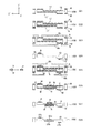
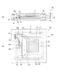
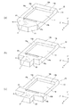
図1は、本発明の振動素子の一実施形態に係る圧電振動素子の構成を示す概略図である。同図(a)は平面図であり、(b)はP−P断面を+X軸方向からみた断面図であり、(c)はQ−Q断面を+Z’方向から見た断面図であり、(d)、(e)、及び(f)はスリット形状の変形例を示すQ−Q断面を+Z’方向から見た断面図である。
圧電振動素子1は、薄肉の振動領域を含む薄肉平板状の振動部12(以下、振動部12とする)、及び振動部12に連設された厚肉部13を有する基板としての圧電基板10と、振動部12の両主面に夫々対向して形成された励振電極25a、25bと、励振電極25a、25bから夫々厚肉部13に延長形成されたリード電極27a、27bと、リード電極27a、27bの夫々の終端に接続されたパッド電極29a、29bと、を備えている。
ここで、両主面とは、一方の主面(表面ともいう)と、一方の主面に対する裏側の主面(裏面、又は他方の主面ともいう)と、を合わせたものをいう。また、振動領域とは、振動エネルギーが閉じ込められている領域、即ち振動エネルギーがほぼ零となる領域の内側を言い、X軸方向の振動領域の寸法と、Z’軸方向の振動領域の寸法との比は周知のように、1.26:1である。また、振動部12とは振動領域とその周縁部とを含んだ薄肉の部分をいう。
Hereinafter, embodiments of the present invention will be described in detail with reference to the drawings.
[First Embodiment of Vibration Element]
FIG. 1 is a schematic diagram illustrating a configuration of a piezoelectric vibration element according to an embodiment of the vibration element of the present invention. The figure (a) is a top view, (b) is a sectional view which looked at PP section from + X-axis direction, (c) is a sectional view which looked at QQ section from + Z 'direction, (D), (e), and (f) are the sectional views which looked at the QQ section which shows the modification of a slit shape from the + Z 'direction.
The
Here, the two main surfaces refer to a combination of one main surface (also referred to as the front surface) and a main surface on the back side of the one main surface (also referred to as the back surface or the other main surface). The vibration region means a region where the vibration energy is confined, that is, the inside of the region where the vibration energy is almost zero, and the size of the vibration region in the X-axis direction and the size of the vibration region in the Z′-axis direction are As is well known, the ratio is 1.26: 1. Moreover, the
圧電基板10は、矩形で、且つ振動部12と、振動部12周縁(外縁)の四辺に沿って振動部12と一体的に設けられた四角い環状で、且つ振動部12よりも厚みが厚い厚肉部13と、を備えている。厚肉部13は、換言すると振動部12の両主面のいずれかから突設されるように設けられている。
厚肉部13は、第1の厚肉部16、第2の厚肉部17、第3の厚肉部15、及び第4の厚肉部14を備えている。
第1の厚肉部16、及び第2の厚肉部17は、振動部12を介して対向する第1の外縁としての辺12c、及び第2の外縁としての辺12d、のそれぞれに沿って設けられている。第4の厚肉部14、及び第3の厚肉部15は、振動部12を介して対向する第4の外縁としての辺12a、及び第3の外縁としての辺12bのそれぞれに沿って設けられている。
二組の対向する辺12c、12dと辺12a、12bは、振動部12を挟んで互いに略平行となるように配置されている。
The
The
The first
The two pairs of opposing
第4の厚肉部14は、第1の厚肉部16、及び第2の厚肉部17のそれぞれの他方の端部の間にある振動部12の辺12aに沿って連設し、両主面側に夫々突設されている。即ち、第4の厚肉部14は、振動部12の−X軸側に形成されている。また、振動部12の辺12aと連設している一方の端縁から−X軸側の他方の端縁へ離間するにつれて厚みが漸増する第4の傾斜部14bと、第4の傾斜部14bの他方の端縁に連設する厚肉四角柱状の第4の厚肉部本体14aと、を備えている。つまり、図1(c)に示すように、第4の厚肉部14は、振動部12の両主面(表面、及び裏面)に突設して形成されている。
同様に、第3の厚肉部15は、第1の厚肉部16、及び第2の厚肉部17のそれぞれの一方の端部の間にある振動部12の辺12bに沿って連設し、両主面に夫々突設されている。即ち、第3の厚肉部15は、振動部12の+X軸側に形成されている。振動部12の辺12bと連設している一方の端縁から+X軸側の他方の端縁へ離間するにつれて厚みが漸増する第3の傾斜部15bと、第3の傾斜部15bの他方の端縁に連設する厚肉四角柱状の第3の厚肉部本体15aと、を備えている。つまり、第3の厚肉部15は、図1(c)に示すように、振動部12の主面の両面(表面、及び裏面)に突設して形成されている。
なお、厚肉部本体(第4の厚肉部本体14a、及び第3の厚肉部本体15a等)とは、Y’軸に略平行な厚みが一定の領域をいう。
The fourth
Similarly, the third
The thick part main body (the fourth thick part
第1の厚肉部16は、振動部12の辺12cに沿って、一方の主面よりも突出して設けられている。即ち、第1の厚肉部16は、表面側において振動部12の+Z’軸側に形成されている。また、振動部12の辺12cと連設している一方の端縁から+Z’軸側の他方の端縁へ離間するにつれて厚みが漸増する第1の傾斜部16bと、第1の傾斜部16bの他方の端縁に連設する厚肉四角柱状の第1の厚肉部本体16aと、を備えている。つまり、第1の厚肉部16の一方の主面は、振動部12の一方の主面(表面)よりも突設して形成されている。そして、第1の厚肉部16の他方の主面と、振動部12の他方の主面(一方の主面に対する裏側の主面)とは連続的に連接されており、同一面となるよう構成されている。なお、振動領域にメサ上の突出したエネルギー閉じ込め領域がある場合についても、振動領域の周縁部の主面が第1の厚肉部16の他方の主面と連続的に連接されており、同一面となるように構成されていればよい。
本実施形態においては、第1の厚肉部16の前記他方の主面と、振動部12の前記他方の主面とは連続的に連接されており、同一面となるよう構成されていることが好ましいが、振動部12への残渣の影響が小さい、すなわち、振動部12の振動領域の有効面積に影響を与えない程度に、第1の厚肉部16の前記他方の主面が、振動部12の前記他方の主面から多少突出していても良い。
The first
In the present embodiment, the other main surface of the first
第2の厚肉部17は、振動部12の辺12dに沿って、一方の主面に対する裏側の主面よりも突出して設けられている。即ち、第1の厚肉部16は、裏面側において振動部12の−Z’軸側に形成されている。また、振動部12の辺12dと連設している一方の端縁から、−Z’軸側の他方の端縁へ離間するにつれて厚みが漸増する第2の傾斜部17bと、第2の傾斜部17bの他方の端縁に連設する厚肉四角柱状の第2の厚肉部本体17aと、を備えている。つまり、第2の厚肉部17の一方の主面は、振動部12の他方の主面(裏面)よりも突設して形成されており、第2の厚肉部17は、振動部12の裏面側において第4の厚肉部14と第3の厚肉部15の他端部間を連接している。そして、第2の厚肉部17の他方の主面と、振動部12の一方の主面と、は連続的に連接されており、同一面となるよう構成されている。なお、振動領域にメサ上の突出したエネルギー閉じ込め領域がある場合についても、振動領域の周縁部の主面が第2の厚肉部17の他方の主面と連続的に連接されており、同一面となるように構成されていればよい。
本実施形態においては、第2の厚肉部17の前記他方の主面と、振動部12の前記他方の主面とは連続的に連接されており、同一面となるよう構成されていることが好ましいが、振動部12への残渣の影響が小さい、すなわち、振動部12の振動領域の有効面積に影響を与えない程度に、第2の厚肉部17の前記他方の主面が、振動部12の前記他方の主面から多少突出していても良い。
The second
In the present embodiment, the other main surface of the second
第1の厚肉部16と第2の厚肉部17とは、図1(b)に示すように振動部12の中心に対して点対称の関係にある。また、第4の厚肉部本体14a、及び第3の厚肉部本体15a夫々の一方の面(表面)と、第1の厚肉部本体16aの一方の面(表面)とは同一平面上にあり、第4の厚肉部本体14a、第3の厚肉部本体15a夫々の他方の面(裏面)と、第2の厚肉部本体17aの面(裏面)とは同一平面上にある。そして、第1、第2、第3及び第4の厚肉部16、17,15、14は夫々の端部が連結されて、四角い環状を形成し、その中央部に振動部12を保持している。
The first
略四角形の振動部12は、その周縁の四辺を第1、第2、第3、及び第4の厚肉部16、17,15、14に包囲されている。つまり、矩形平板状の圧電基板10の両主面からエッチングを進め、両主面に対向する2つの凹陥部を形成し、小型化を図るため不要な部位をカットして、薄肉の振動部12を形成している。
更に、圧電基板10は、第3の厚肉部15に少なくとも一つの応力緩和用のスリット20が貫通形成されている。図1に示した実施形態例では、スリット20は、振動部12の辺12bから離間した第3の傾斜部15bと第3の厚肉部本体15aとの境界部(連接部)に沿って第3の厚肉部本体15aの面内に形成されている。
このように、スリット20を振動部12の辺12bから離間して配置しているので、スリットの形成が容易であり、更に、第3の厚肉部本体15aの前記境界部(連接部)へ寄せて配置したので、第3の厚肉部本体15aの被支持部(パッド電極)29aの面積を広く確保することができ、塗布する導電性接着剤の径を大きくすることができる。これに対して、スリット20が第3の厚肉部本体15aの被支持部(パッド電極)29a寄りに配置されると、被支持部(パッド電極)29aの面積が狭くなり、導電性接着剤の径を小さくしなければならない。その結果、導電性接着剤内に含まれる導電フィラーの絶対量も減り、導電性が悪化し、圧電振動素子1の共振周波数が安定しなくなり周波数変動(通称、F飛び)が発生しやすくなる虞がある。
従って、スリット20は第3の厚肉部本体15aの前記境界部(連接部)へ寄せて配置することが好ましい。
The substantially rectangular vibrating
Further, in the
As described above, since the
Therefore, it is preferable that the
なお、スリット20は、図1(c)に示すような貫通形成されたものに限らず底部を有した溝状のスリットであってもよい。溝状のスリットについて詳述すると、例えば、図1(d)に示すように、第3の厚肉部15の裏面側から形成されて底部を有する第1のスリット20a’、及び第3の厚肉部15の表面側から形成されて底部を有する第2のスリット20b’の、表裏両面側から設けられたスリットで構成されてもよい。また、図1(e)に示すように、第3の厚肉部15の裏面側から形成されて底部を有する第3のスリット20c’で構成されてもよい。また、図1(f)に示すように、第3の厚肉部15の表面側から形成されて底部を有する第4のスリット20d’が設けられている構成でもよい。
また、本発明に係るスリットは平面視で第3の厚肉部15で囲まれており、図1(d)〜図1(f)に示すようなスリットが有底の溝である場合、スリットの底部の厚みが振動部の厚みよりも厚くても良いし、また逆に薄くても良い。
ここで説明したスリット20の形状は、以降説明する他の実施形態、変形例、および応用例においても適用可能である。
The
In addition, the slit according to the present invention is surrounded by the third
The shape of the
圧電基板10の一例としては、水晶等の圧電材料は三方晶系に属し、図2に示すようにX軸(電気軸)、Y軸(機械軸)、Z軸(光学軸)からなる直交座標系のX軸を中心として、Z軸をY軸の−Y方向へ傾けた軸をZ’軸とし、Y軸をZ軸の+Z方向へ傾けた軸をY’軸とし、X軸とZ’軸に平行な面で構成され、Y’軸に平行な方向を厚みとする回転Yカット水晶基板である。本実施形態では回転Yカット水晶基板の一例であるATカット水晶基板を用いて説明している。
As an example of the
ATカット水晶基板は、図2に示すようにXZ面をX軸の回りに角度θだけ回転させた平面に沿って、水晶から切り出された平板である。ATカット水晶基板の場合は、θは略35°15′である。なお、Y軸及びZ軸もX軸の周りにθ回転させて、夫々Y’軸、及びZ’軸とする。従って、ATカット水晶基板は、直交する結晶軸X、Y’、Z’を有する。ATカット水晶基板は、厚み方向がY’軸であって、Y’軸に直交するXZ’面(X軸及びZ’軸を含む面)が主面であり、厚みすべり振動が主振動として励振される。
尚、本発明に係る圧電基板は、前記角度θが略35°15′のATカットに限定されるものではなく、厚みすべり振動を励振するBTカット、等の圧電基板にも広く適用できるのは言うまでもない。
The AT-cut quartz substrate is a flat plate cut out from quartz along a plane obtained by rotating the XZ plane about the X axis by an angle θ as shown in FIG. In the case of an AT-cut quartz substrate, θ is approximately 35 ° 15 ′. Note that the Y-axis and the Z-axis are also rotated by θ around the X-axis to be the Y′-axis and the Z′-axis, respectively. Accordingly, the AT-cut quartz substrate has crystal axes X, Y ′, and Z ′ that are orthogonal to each other. The AT-cut quartz substrate has a Y 'axis in the thickness direction, and an XZ ′ plane (plane including the X axis and Z ′ axis) orthogonal to the Y ′ axis is the main surface, and thickness shear vibration is excited as the main vibration. Is done.
The piezoelectric substrate according to the present invention is not limited to the AT cut with the angle θ of approximately 35 ° 15 ′, but can be widely applied to a piezoelectric substrate such as a BT cut that excites thickness shear vibration. Needless to say.
圧電基板10は、図1(a)に示すように、Y’軸に平行な方向(以下、「Y’軸方向」という)を厚み方向として、X軸に平行な方向(以下、「X軸方向」という)を長辺とし、Z’軸に平行な方向(以下、「Z’軸方向」という)を短辺とする矩形の形状を有する。
圧電基板10を駆動する励振電極25a、25bは、図1に示す実施形態例では四角形状であり、振動部12のほぼ中央部の表裏両面に対向して形成されている。図1(b)に示すように、裏面側の励振電極25bの面積は、表面側の励振電極25aの面積に対し、十分に大きく設定する。これは、励振電極の質量効果によるエネルギー閉じ込め係数を、必要以上に大きくしないためである。つまり、裏面側の励振電極25bの面積を十分に大きくすることにより、プレートバック量Δ(=(fs−fe)/fs、ここでfsは圧電基板のカットオフ周波数、feは圧電基板全面に励振電極を付着した場合の周波数)は、表面側の励振電極25aの質量効果のみに依存する。
As shown in FIG. 1A, the
In the embodiment shown in FIG. 1, the
励振電極25a、25bは、蒸着装置、あるいはスパッター装置等を用いて、下地にニッケル(Ni)を成膜し、その上に金(Au)を重ねて成膜する。金(Au)の厚さは、オーミックロスが大きくならない範囲で、主振動のみを閉じ込めモード(S0)とし、斜対称インハーモニックモード(A0、A1・・)及び対称インハーモニックモード(S1、S3・・)を、閉じ込めモードとしないことが望ましい。しかし、例えば490MHz帯の圧電振動素子では、電極膜厚のオーミックロスを避けるように成膜すると、低次のインハーモニックモードがある程度、閉じ込められることは避けられない。
表面側に形成した励振電極25aは、振動部12上から第1の傾斜部16bと、第1の厚肉部本体16aとの表面上を経由して第3の厚肉部本体15aの表面まで形成されるリード電極27aにより、第3の厚肉部本体15aの表面に形成されたパッド電極29aに導通接続されている。また、裏面側に形成された励振電極25bは、振動部12上から第2の傾斜部17bと、第2の厚肉部本体17aとの表面上を経由して第3の厚肉部本体15aの裏面まで形成されるリード電極27bにより、第3の厚肉部本体15aの裏面に形成されたパッド電極29bに導通接続されている。
The
The
図1(a)に示した実施形態例は、リード電極27a、27bの引出し構造の一例であり、リード電極27aは他の支持部を経由してもよい。ただ、リード電極27a、27bの長さは最短であることが望ましく、リード電極27a、27bどうしが交差しないように配慮することにより、静電容量の増加を抑えることが望ましい。静電容量の増加は圧電振動素子1の容量比γ(直列容量(モーショナルキャパシタンス)C1に対する並列容量(静電容量)C0の比)を悪化させる。
また、図1の実施形態例では、圧電基板10の表裏両面に近接して夫々パッド電極29a、29bを形成する例を示した。圧電振動素子1をパッケージに収容する際に、圧電振動素子1を裏返し、パッド電極29aを固定し、パッド電極29bと、パッケージの電極端子とをボンディングワイヤーで接続する。このように支持する部位が一点になると、導電性接着剤に起因して生じる応力を小さくすることが可能である。
また、圧電振動素子1のパッド電極29a、29bを、上記例よりも大きな間隔をあけて形成してもよい。
The embodiment shown in FIG. 1A is an example of a lead-out structure of the
In the embodiment shown in FIG. 1, an example is shown in which the
Further, the
振動部12と、圧電振動素子1の被支持部であるパッド電極29a、29bとの間にスリット20を設ける理由は、導電性接着剤の硬化時に発生する応力の広がりを防止することにある。
即ち、導電性接着剤を用いて圧電振動素子1のパッド電極29a、29bをパッケージに支持する場合には、まず第3の厚肉部本体15aの被支持部(パッド電極)29aに導電性接着剤を塗布し、これを反転してパッケージ等の素子搭載パッドに載置し、少し押さえる。導電性接着剤を硬化させるために高温の炉内に所定の時間保持する。高温状態では第3の厚肉部本体15a、及びパッケージも共に膨張し、接着剤も一時的に軟化するので、被支持部(パッド電極)29aには応力は生じない。導電性接着剤が硬化した後、第3の厚肉部本体15a、及びパッケージが冷却してその温度が常温(25℃)に戻ると、導電性接着剤、パッケージ、及び第3の厚肉部本体15aの各線膨張係数の差により、硬化した導電性接着剤から生じる応力が被支持部(パッド電極)29aに伝わり、更に第3の厚肉部本体15aから第4の厚肉部14及び第1の厚肉部16、振動部12へと広がる。この応力の広がりを防止するために応力緩和用のスリット20を設けている。
The reason why the
That is, when the
スリット20の形成部位と圧電基板10に生じる応力(∝歪)分布との関係は、有限要素法を用いたシミュレーションで解析するのが一般的である。振動部12における応力が少ない程、周波数温度特性、周波数再現性、周波数エージング特性の優れた圧電振動素子が得られる。
導電性接着剤としては、シリコーン系、エポキシ系、ポリイミド系、ビスマレイミド系等があるが、圧電振動素子1の脱ガスによる周波数経年変化を考慮に入れて、ポリイミド系の導電性接着剤を用いる。ポリイミド系の導電性接着剤は硬いので、圧電振動素子1を離れた二カ所で支持するよりも一カ所で支持する方が、発生する応力の大きさを低減できる。目標とする490MHz帯の電圧制御型圧電発振器(Voltage Controlled Crystal Oscillator:VCXO)用の圧電振動素子1には、一カ所支持を用いた。
つまり、パッド電極29aに導電性接着を塗布し、反転して収容するパッケージの素子搭載パッドに載置し、乾燥して固定・接続し、他方のパッド電極29bにはボンディングワイヤーを用いて導通・接続することにした。図1(a)に示すように、パッド電極29aと、パッド電極29bとは、ほぼ対向して形成されているので、一カ所支持となる。
The relationship between the formation site of the
Examples of the conductive adhesive include silicone-based, epoxy-based, polyimide-based, and bismaleimide-based. A polyimide-based conductive adhesive is used in consideration of frequency aging due to degassing of the
That is, a conductive adhesive is applied to the
図1に示した圧電基板10は、X軸方向の長さがZ’軸方向の長さより長い、所謂Xロングとした。これは周知のように、ATカット水晶基板のX軸方向の両端に力を加えたときの周波数変化と、Z’軸方向の両端に同じ力を加えたときの周波数変化と、を比べると、Z’軸方向の両端に力を加えたときの方が周波数変化は小さい。つまり、支持点はZ’軸方向に沿って設ける方が、応力による周波数変化は小さくなり、圧電振動素子としては好ましい。
また、図1に示した実施形態例では、薄肉の振動部12は矩形となっているが、薄肉の振動部12の第1の厚肉部16に連接する辺12cの両端部に相当する両角隅部が面取りされていてもよい。
The
In the embodiment shown in FIG. 1, the thin vibrating
図1の実施形態例では、励振電極25a、25bの形状として四角形、つまり正方形、または矩形(X軸方向を長辺とする)の例を示したが、本発明の圧電振動素子1に用いる励振電極は、これに限定する必要はない。
図3に示す実施形態例は、図中表面側の励振電極25aが円形であり、図中裏面側の励振電極25bは、励振電極25aより十分に大きな四角形である。なお、裏面側の励振電極25bも十分に大きな円形であってもよい。
図4に示す実施形態例は、図中表面側の励振電極25aが楕円形であり、図中裏面側の励振電極25bは、励振電極25aより十分に面積が大きい四角形である。弾性定数の異方性によりX軸方向の変位分布と、Z’軸方向の変位分とが異なり、変位分布をX−Z’平面に平行な面で切った切断面は、楕円形になる。そのため、楕円形状の励振電極25aを用いた場合が最も効率よく、圧電振動素子1を駆動できる。即ち、圧電振動素子1の容量比γ(=C0/C1、ここで、C0は静電容量、C1は直列共振容量)を最小にできる。
また、励振電極25aは長円形であってもよい。
In the embodiment shown in FIG. 1, the
In the embodiment shown in FIG. 3, the
In the embodiment shown in FIG. 4, the
The
[振動素子の第2の実施形態]
図5は、振動素子の第2の実施形態に係る圧電振動素子2の構成を示す概略図である。図5(a)は圧電振動素子2の平面図であり、同図(b)はP−P断面を+X軸方向からみた断面図であり、同図(c)はQ−Q断面を+Z’軸方向からみた断面図である。
圧電振動素子2が図1に示す圧電振動素子1と異なる点は、応力緩和用のスリット20を設ける位置にある。本実施形態例では、スリット20が薄肉の振動部12の辺12bより離間した第3の傾斜部15b内に形成されている。圧電振動素子1のように、振動部12の辺12bに沿って、スリット20の一方の端縁が、辺12bに接するように第3の傾斜部15b内にスリット20を形成するのではなく、第3の傾斜部15bの両端縁より離間してスリット20を設けている。つまり第3の傾斜部15bには、振動部12の辺12bの端縁と連接する極細の傾斜部15b’が残されている。換言すれば、辺12aとスリット20との間に極細の傾斜部15b’が形成されている。
[Second Embodiment of Vibration Element]
FIG. 5 is a schematic diagram illustrating a configuration of the
The
極細の傾斜部15b’を残した理由は次の通りである。即ち、振動部12に励振電極25a、25bを形成して高周波電圧を印加し励振すると、主振動(S0)の他にインハーモニックモード(A0、S1、A1、S2・・)が励振される。望ましいのは主振動(S0)モードのみを閉じ込めモードとし、他のインハーモニックモードは伝搬モード(非閉じ込めモード)とすることである。しかし、振動部12が薄く成り、その基本波周波数が数百MHzとなると、電極膜のオーミックロスを避けるため、励振電極25a、25bの膜厚を所定の厚さ以上にする必要がある。このため、プレートバック量が大きくなり、主振動に近接したインハーモニックモードがエネルギー閉じ込めモードになる。この低次のインハーモニックモードの振幅の大きさ(CI値に比例)を抑制するには、インハーモニックモードの定在波が成り立つ条件を妨げるようにすればよい。つまり、図5の振動部12のZ’軸方向の両端縁の形状は、図5(b)に示すように振動部12の重心に対して点対称であり、またX軸方向の両端縁の形状も極細の傾斜部15b’を残したことにより非対称となり、低次のインハーモニックモード定在波の振幅を抑えることができる。
The reason for leaving the ultra-thin
[振動素子の第3の実施形態]
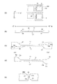
図6は、振動素子の第3の実施形態に係る圧電振動素子3の構成を示す概略図である。図6(a)は圧電振動素子3の平面図であり、同図(b)はP−P断面を+X軸方向からみた断面図であり、同図(c)はQ−Q断面を+Z’軸方向からみた断面図である。
圧電振動素子3が図1に示す圧電振動素子1と異なる点は、第3の厚肉部15に2個の応力緩和用のスリット20a、20bが並行して設けられている点である。即ち、第3の厚肉部本体15aの面内に第1のスリット20aが設けられると共に、第3の傾斜部15bの面内に第2のスリット20bが形成されている。
第3の厚肉部本体15aの面内、及び第3の傾斜部15bの面内に夫々個別のスリットを形成することで、圧電振動素子3を接着・固定する際に生じる応力の広がりをよりよく抑圧することができ、周波数再現性、周波数温度特性、CI温度特性、及び周波数エージング特性に優れた圧電振動素子3が得られる。
[Third Embodiment of Vibration Element]
FIG. 6 is a schematic diagram illustrating a configuration of the
The piezoelectric vibrating
By forming individual slits in the surface of the third thick portion
図6(a)に示す平面図のように、第1のスリット20a、及び第2のスリット20bを単にX軸方向に並置するのではなく、図7(a)の平面図に示すように、Z’軸方向に互い違いになるようにずらして配置してもよい。2個のスリット20a、20bを設けた圧電振動素子3の方が、導電性接着剤に起因して生じる応力を、振動部12まで広げないように抑圧する効果を高めることが可能である。また、図7(b)に示す変形例の構成は、図1、図6に夫々示すスリット20、20a、20bの効果を合わせ持つようにした圧電振動素子3であり、スリット20は、第3の傾斜部15bと第3の厚肉部本体15aとに跨って構成されている。
As shown in the plan view of FIG. 6A, the
[振動素子の第4の実施形態]
図8は、振動素子の第4の実施形態に係る圧電振動素子4の構成を示す概略図である。図8(a)は圧電振動素子4の平面図であり、(b)はP−P断面を+X軸方向からみた断面図であり、(c)はQ−Q断面を+Z’軸方向からみた断面図である。
圧電振動素子4は、矩形で薄肉の振動領域を含む振動部12、及び振動部12と一体化され振動部12よりも厚い厚肉部13を有する圧電基板10と、振動部12の表面及び裏面(両主面)に夫々配置された励振電極25a、25bと、各励振電極25a、25bから夫々の厚肉部13に設けられたパッド電極29a、29bに向けて夫々延在して設けられたリード電極27a、27bと、を備えている。
[Fourth Embodiment of Vibration Element]
FIG. 8 is a schematic diagram showing the configuration of the
The
厚肉部13は、振動部12の辺12aに沿って連設され、且つ両主面側に夫々突設(突出)した第3の厚肉部15と、振動部12の辺12aの一端部に連続する辺12bに沿って連設され、且つ振動部12の一方の主面側(表面側)において、第3の厚肉部15の一端部と連設された第1の厚肉部16と、を備えている。更に、厚肉部13は、振動部12の辺12aの他端部に連続する辺12cに沿って連設され、且つ振動部12の他方の主面側(裏面側)において、第3の厚肉部15の他端部と連設された第2の厚肉部17と、を備えている。つまり、圧電基板10は、振動部12の三辺12a、12b、12cに沿って一体化された厚肉の厚肉部13(第1の厚肉部16、第2の厚肉部17、第3の厚肉部15)を備えており、第1の厚肉部16と第2の厚肉部17とは、振動部12の重心に関して点対称に配置されている。前記2つの辺12b、12cは対向し、振動部12を挟んで互いに略平行となるように配置されている。
The
第1の厚肉部16の一方の主面は、振動部12の一方の主面(表面)よりも突設して形成されている。そして、第1の厚肉部16の他方の主面と振動部12の他方の主面とは連続的に連接されており、同一面となるよう構成されている。
第2の厚肉部17の一方の主面は、振動部12の他方の主面(裏面)よりも突設して形成されている。そして、第2の厚肉部17の他方の主面と振動部12の一方の主面とは連続的に連接されており、同一面となるよう構成されている。
なお、振動領域にメサ状の突出したエネルギー閉じ込め領域がある場合についても、振動領域の周縁部の主面が第2の厚肉部17の他方の主面と連続的に連接されており、同一面となるように構成されていればよい。
One main surface of the first
One main surface of the second
Even in the case where there is a mesa-shaped protruding energy confinement region in the vibration region, the main surface of the peripheral portion of the vibration region is continuously connected to the other main surface of the second
第3の厚肉部15は、振動部12の辺12aに連設し、振動部12の辺12aに連接する一方の端縁(内側端縁)から他方の端縁(外側端縁)に向かって離間するにつれて厚みが漸増する第3の傾斜部15bと、第3の傾斜部15bの前記他方の端縁(外側端縁)に連設する厚肉四角柱状の第3の厚肉部本体15aと、を備えている。
同様に、第1の厚肉部16は、振動部12の辺12bに連設し、振動部12の辺12bに連接する一方の端縁(内側端縁)から他方の端縁(外側端縁)に向かって離間するにつれて厚みが漸増する第1の傾斜部16bと、第1の傾斜部16bの前記他方の端縁(外側端縁)に連設する厚肉四角柱状の第1の厚肉部本体16aと、を備えている。
また、第2の厚肉部17は、振動部12の辺12cに連設し、振動部12の辺12cに連接する一方の端縁(内側端縁)から他方の端縁(外側端縁)に向かって離間するにつれて厚みが漸増する第2の傾斜部17bと、第2の傾斜部17bの前記他方の端縁(外側端縁)に連設する厚肉四角柱状の第2の厚肉部本体17aと、を備えている。
そして、第3の厚肉部15には少なくとも一つのスリット20が貫通形成されている。
The third
Similarly, the first
The second
In addition, at least one slit 20 is formed through the third
第3の厚肉部15、及び第1の厚肉部16の夫々の一方の面(表面側)は、同一平面上、即ち図8に示す座標軸のX−Z’平面上にあり、第3の厚肉部15の他方の面(裏面側)と第2の厚肉部17の裏面とは、同一平面上(X−Z’平面上)にある。
言い換えると、振動部12の他方の主面(裏面)と、第1の厚肉部16の他方の面(裏面)とは、同一平面上にあり、振動部12の一方の主面(表面)と、第2の厚肉部17の他方の面(表面)とは、同一平面上にある。つまり、不要な厚肉部を低減している。
また、第3の厚肉部15は、振動部12の表裏面(両面)に突設されている。また、第1の厚肉部16及び第2の厚肉部17は、夫々が、図8(b)に示されているように振動部12の中心に対し点対称となるように、圧電基板の片面側にのみに突設されている。
そして、第3の厚肉部15には、少なくとも一つの応力緩和用のスリット20が、振動部12と、被支持部であるパッド電極29a、29bとの間に、Z’軸方向に沿って貫通形成されている。図8に示した実施形態例では、スリット20は、第3の傾斜部15bと第3の厚肉部本体15aとの境界部(連接部)に沿って、第3の厚肉部本体15a内に形成されている。
なお、厚肉部本体(15a、16a、17a)とは、Y’軸方向の厚みが一定の領域をいう。
One surface (surface side) of each of the third
In other words, the other main surface (back surface) of the
Further, the third
The third
The thick part main body (15a, 16a, 17a) refers to a region having a constant thickness in the Y′-axis direction.
また、スリット20は、図8(c)に示すような貫通形成されたものに限らず底部を有した溝状のスリットであってもよい。溝状のスリットについて詳述すると、例えば、図8(d)に示すように、第3の厚肉部15の表面側から形成されて底部を有する第1のスリット20a’、及び第3の厚肉部15の裏面側から形成されて底部を有する第2のスリット20b’の、表裏両面側から設けられたスリットで構成されてもよい。また、図8(e)に示すように、第3の厚肉部15の表面側から形成されて底部を有する第3のスリット20c’で構成されてもよい。また、図8(f)に示すように、第3の厚肉部15の裏面側から形成されて底部を有する第4のスリット20d’が設けられている構成でもよい。
ここで説明したスリット20の形状は、以降説明する他の実施形態、変形例、および応用例においても適用可能である。
Further, the
The shape of the
圧電基板10を駆動する励振電極25a、25b、およびリード電極27a、27bなどの電極の構成、スリット20を設ける理由など、前述の第1の実施形態と同様な説明は省略する。
Descriptions similar to those in the first embodiment, such as the configuration of the electrodes such as the
図9は、圧電振動素子4の構成部材を示す平面図である。図9(a)は、圧電基板10上に形成されたリード電極27a、27b、及びパッド電極29a、29bの配置、構成を示す平面図であり、同図(b)は励振電極25a、25bの配置、構成を示す平面図である。リード電極27aは、表面側の想定する励振電極25aの端縁から延在され、第1の厚肉部16の表面を経由し、第3の厚肉部15の中央部の表面に設けられたパッド電極29aに接続するように形成する。また、リード電極27bは、裏面側の想定する励振電極25bの端縁から延在され、裏面側の第2の厚肉部17の表面を経由し、第3の厚肉部15の中央部の裏面に設けられたパッド電極29bに接続するように形成する。
リード電極27a、27bは、クロム(Cr)の薄膜から成る第1層と、この第1層上に積層された金(Au)の薄膜から成る第2層と、を備えている。リード電極27aの一部を拡大したR−R線断面図を、図9(a)中、左側の破線円27Aの中に示す。リード電極27aは、第1の厚肉部16、及び第3の厚肉部15の表面側(上面側)にクロム(Cr)の薄膜27cを下地とし、この上に金(Au)の薄膜27gを積層成膜して、構成する。リード電極27bについても同様に構成する。
FIG. 9 is a plan view showing components of the
Each of the
また、第3の厚肉部15の中央部の表裏面に設けられたパッド電極29a、29bは、クロム(Cr)の薄膜から成る第1層と、この第1層上に積層された金(Au)の薄膜から成る第2層と、を備えている。パッド電極29aの一部を拡大したT−T線断面図を、図9(a)中、下部の破線円29Aの中に示す。パッド電極29aは、第3の厚肉部15の表面側(上面側)にクロム(Cr)の薄膜29cを下地とし、この上に金(Au)の薄膜29gを積層成膜して構成する。パッド電極29bについても同様に構成する。
リード電極27a、27b、及びパッド電極29a、29bは、同一工程で形成されるため、膜厚の一例は、第1層目のクロム(Cr)の薄膜27c、29cが100Å(1Å=0.1nm(ナノメートル))、第2層目の金(Au)の薄膜27g、29gが2000Åと厚く形成されている。このため、リード電極27a、27b、及びパッド電極29a、29bのオーミックロスは生ぜず、ボンディング強度も十分である。
なお、クロム(Cr)薄膜と金(Au)薄膜との間に、他の金属膜を挟んだ構成でもよい。
The
Since the
Note that another metal film may be sandwiched between a chromium (Cr) thin film and a gold (Au) thin film.
図9(b)は、前工程で形成されたリード電極27a、27bと整合するように、圧電基板10上に形成した励振電極25a、25bの配置、構成を示す平面図である。圧電基板10の表面側に励振電極25aを形成し、裏面側に励振電極25aの面積より十分に大きく、且つ励振電極25aが面積内に納まる励振電極25bを形成する。励振電極25a、25bの構成の一例は、ニッケル(Ni)の薄膜から成る第1層と、この第1層上に積層された金(Au)の薄膜から成る第2層と、を備えている。励振電極25a、25bの一部、破線円のU−U線断面図を、図9(b)中、右側の破線円内に示す。振動部12の表裏面の第一層目にニッケル(Ni)の薄膜25nが成膜され、第二層目に金(Au)の薄膜25gが、積層して成膜されている。膜厚の一例は、第1層目のニッケル(Ni)の薄膜25nが70Åであり、第2層目の金(Au)の薄膜25gが600Åである。
なお、ニッケル(Ni)薄膜と、金(Au)薄膜との間に他の金属膜を挟んだ構成でもよい。
FIG. 9B is a plan view showing the arrangement and configuration of the
Note that another metal film may be sandwiched between a nickel (Ni) thin film and a gold (Au) thin film.
リード電極27a、27b、及びパッド電極29a、29bと、励振電極25a、25bとの夫々の電極材料、及び電極膜厚を異ならせる理由を以下に説明する。圧電基板10の振動部12の基本波周波数を、例えば490MHzとする。リード電極27a、27b、パッド電極29a、29b、及び励振電極25a、25bを、例えば第1層目に70Åのニッケル(Ni)の薄膜、第2層目に600Åの金(Au)の薄膜で構成したとする。主振動は十分に閉じ込めモードとなり、そのクリスタルインピーダンス(CI;等価抵抗)は、小さくなることが期待される。しかし、リード電極27a、27bの金(Au)の膜厚が薄いために、薄膜のオーミックロスが生じ、圧電振動素子4のCI値が大きくなる虞がある。更に、パッド電極29a、29bが、70Åのニッケル(Ni)の薄膜と、600Åの金(Au)の薄膜との構成では、ワイヤボンディングの強度不足を来たす虞がある。
The reason why the electrode materials and the electrode film thicknesses of the
また、リード電極27a、27b、パッド電極29a、29b、及び励振電極25a、25bを、例えば第1層目に70Åのクロム(Cr)の薄膜、第2層目に600Åの金(Au)の薄膜で構成したとすると、金(Au)の薄膜が薄いため、熱によりクロム(Cr)が金(Au)の薄膜内に拡散し、薄膜のオーミックロスが生じ、主振動のCI値が大きくなる虞がある。
Further, the
そこで、リード電極27a、27b、及びパッド電極29a、29bと、励振電極25a、25bとの形成工程を分離し、且つ夫々の電極薄膜の材料、及び膜厚を、夫々の薄膜の機能に最適になるように設定することにした。つまり、励振電極25a、25bは、主振動を閉じ込めモードとし、近接したインハーモニック・オーバートーンモードはできるだけ伝搬モード(非閉じ込めモード)となるように、例えば励振電極25a、25bの膜厚をニッケル(Ni)の薄膜を70Å、金(Au)の薄膜を600Åと薄く設定した。一方、リード電極27a、27b、及びパッド電極29a、29bは、細いリード電極の膜抵抗を低減し、且つボンディングの接着強度を高めるべく、クロム(Cr)の膜厚を100Å、金(Au)の膜厚を2000Åと厚めに設定した。
Therefore, the formation process of the
上記の膜厚は一例であり、本発明ではこの数値に限定するものではなく、振動部12の周波数の違いに応じて変更される。要は、エネルギー閉じ込め理論と、薄膜のオーミックロスとを考慮して、励振電極25a、25bには、最適膜厚のニッケル(Ni)及び金(Au)の積層膜を用いればよい。また、リード電極27a、27b、及びパッド電極29a、29bの膜厚は、薄膜のオーミックロスと、ボンディング強度とを考慮して、必要な厚さのクロム(Cr)と金(Au)の積層膜を用いればよい。
励振電極25a、25b、リード電極27a、27b、及びパッド電極29a、29bの製造方法については後述する。
The above film thickness is an example, and the present invention is not limited to this value, and is changed according to the difference in the frequency of the vibrating
A method for manufacturing the
図8に示す第4の実施形態例では、励振電極25a、25bの形状として四角形、つまり正方形、または矩形(X軸方向を長辺とする)の例を示したが、これに限定する必要はない。
図10に示す実施形態例は、表面側の励振電極25aが円形であり、裏面側の励振電極25bは、励振電極25aの面積より十分に大きく、且つ励振電極25aがその面積内に納まる四角形の電極である。また、裏面側の励振電極25bは、面積の十分に大きな円形であってもよい。
図11に示す実施形態例は、表面側の励振電極25aが楕円形であり、裏面側の励振電極25bは、励振電極25aの面積より十分に大きく、且つ励振電極25aがその面積内に納まる四角形の電極である。圧電基板10が水晶の場合、弾性定数の異方性によりX軸方向の変位分布と、Z’軸方向の変位分が異なり、変位分布をX−Z’平面に平行な面で切った切断面は、楕円形になる。そのため、楕円形状の励振電極25aを用いた場合が最も効率よく、圧電振動素子4を駆動できる。即ち、圧電振動素子4の容量比γ(=C0/C1、ここで、C0は静電容量、C1は直列共振容量)を最小にできる。また、励振電極25aは長円形であってもよい。また、裏面側の励振電極25bは、励振電極25aの面積より十分に大きく、且つ励振電極25aがその面積内に納まる円形、楕円形、長円等であってもよい。
In the fourth embodiment shown in FIG. 8, the
In the embodiment shown in FIG. 10, the
In the embodiment shown in FIG. 11, the
[振動素子の第5の実施形態]
図12は、振動素子の第5の実施形態に係る圧電振動素子の構成を示す概略図である。図12(a)は圧電振動素子6の平面図であり、(b)はP−P断面を+X軸方向からみた断面図であり、(c)はQ−Q断面を+Z’軸方向からみた断面図である。
圧電振動素子6が、図8に示す圧電振動素子4と異なる点は、応力緩和用のスリット20を設ける位置にある。本例では、スリット20は、薄肉の振動部12の辺12aの端縁より離間した第3の傾斜部15b内に貫通形成設されている。圧電振動素子4のように、振動部12の辺12aに沿って、スリット20の一方の端縁が辺12aに接するように、第3の傾斜部15b内にスリット20を形成するのではなく、第3の傾斜部15bの両端縁より離間してスリット20を設けている。つまり第3の傾斜部15bには、振動部12の辺12aの端縁と連接する極細の傾斜部15bbが残されている。換言すれば、辺12aとスリット20との間に極細の傾斜部15bbが形成されている。
[Fifth Embodiment of Vibration Element]
FIG. 12 is a schematic diagram illustrating a configuration of a piezoelectric vibration element according to the fifth embodiment of the vibration element. 12A is a plan view of the
The piezoelectric vibrating
極細の傾斜部15bbを残した理由は次の通りである。即ち、振動部12に配置された励振電極25a、25bに高周波電圧を印加して振動部12を励振すると、主振動(S0)の他にインハーモニック・オーバートーンモード(A0、S1、A1、S2・・)が励振される。望ましくは、主振動(S0)モードのみを閉じ込めモードとし、他のインハーモニック・オーバートーンモードは伝搬モード(非閉じ込めモード)とすることである。しかし、振動部12が薄く成り、その基本波周波数が数百MHzと高くなると、電極膜のオーミックロスを避けるため、励振電極25a、25bは所定の厚さ以上にする必要がある。このため、励振電極25a、25bの厚みを前記所定の厚さ以上とした場合に、主振動に近接した低次のインハーモニック・オーバートーンモードが閉じ込めモードになる。
この低次のインハーモニック・オーバートーンモードの振幅の大きさ(CI)を抑制するには、インハーモニック・オーバートーンモードの定在波が成り立つ条件を、妨げるようにすればよい。つまり、図12の振動部12のX軸方向の両端縁の形状が、細片(極細の傾斜部15bb)を残したため非対称となり、低次のインハーモニック・オーバートーンモードの定在波の振幅が、抑えられることができる。
The reason for leaving the ultra-thin inclined portion 15bb is as follows. That is, when the
In order to suppress the magnitude (CI) of the amplitude of the low-order inharmonic overtone mode, it is only necessary to prevent the condition that the standing wave of the inharmonic overtone mode is established. That is, the shape of the both end edges in the X-axis direction of the
[振動素子の第6の実施形態]
図13は、振動素子の第6の実施形態に係る圧電振動素子の構成を示す概略図である。図13(a)は圧電振動素子7の平面図であり、(b)はP−P断面を+X軸方向からみた断面図であり、(c)はQ−Q断面を+Z’軸方向からみた断面図である。
圧電振動素子7が、図8に示す圧電振動素子4と異なる点は、2個の応力緩和用のスリットを設けた点にある。つまり、第3の厚肉部本体15a内に、第1のスリット20aが貫通形成されていると共に、第3の傾斜部15b内に、第2のスリット20bが貫通形成されている。第3の厚肉部本体15a内、及び第3の傾斜部15b内に夫々個別のスリット20a、20bを設ける目的は、既に説明しているので、ここでは省略する。
[Sixth Embodiment of Vibration Element]
FIG. 13 is a schematic diagram illustrating a configuration of a piezoelectric vibration element according to a sixth embodiment of the vibration element. 13A is a plan view of the
The piezoelectric vibrating
図14は、図13に示した圧電振動素子7の変形例の構成を示す平面図である。圧電振動素子7’において、第1のスリット20aは、第3の厚肉部本体15a内に貫通形成設され、第2のスリット20bは、第3の傾斜部15b内に貫通形成されている。しかし、第1のスリット20a、及び第2のスリット20bは、図13(a)に示す平面図のように、第1のスリット20a、及び第2のスリット20bをX軸方向に並置するのではなく、Z’軸方向に互い違いになるように段差状にずらして配置されている点が、圧電振動素子7と異なる。2個のスリット20a、20bを設けることにより、導電性接着剤に起因して生じる応力を、振動部12まで広げないようにすることができる。
FIG. 14 is a plan view showing a configuration of a modification of the
図15は、図8に示した実施形態例の圧電振動素子4の変形例の構成を示す平面図である。圧電振動素子4’において、リード電極27aは、表面の励振電極25aの端縁から延在され、第1の厚肉部16の表面(上面)を経由し、第3の厚肉部15の表面に設けられたパッド電極29aに接続する構成である。また、リード電極27bは、裏面側の励振電極25bの端縁から延在され、第2の厚肉部17の表面側を経由し、第3の厚肉部15の裏面側に設けられたパッド電極29bに連設する構成である。
図8に示した実施形態例の圧電振動素子4と異なる点は、パッド電極29a、29bが配置される位置にある。パッド電極29a、29bは第3の厚肉部本体15aの表面に、互いに離れて設けられている。パッド電極29bは、裏面に形成されたリード電極27bと導通するように、裏面から圧電基板10の端縁に跨って表面まで導体薄膜により形成されている。表面側のパッド電極29a、29bに導電性接着剤を塗布し、これを反転してパッケージの素子搭載パッドに載置する際に、容易に導通が図られるように、パッド電極29a、29bが構成されている。
FIG. 15 is a plan view showing a configuration of a modification of the
A difference from the
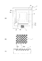
[振動素子の製造方法]
(素子の外形形成工程)
図16は、圧電基板10の両面に凹陥部11、11’を形成すると共に、圧電基板10の外形及びスリット20の形成に係る概略製造工程図である。ここでは、圧電ウェハーとして水晶ウェハーを例にし、水晶ウェハー10W上に複数の圧電振動素子1を形成する製造工程を説明するが、断面図では、個片化される圧電振動素子1の形成工程を示している。
工程S1では、両(表裏)面がポリッシュ加工された所定の厚さ、例えば80μmの水晶ウェハー10Wを、十分に洗浄し乾燥した後、表裏面にスパッタリング等により、クロム(Cr)を下地にし、その上に金(Au)を積層した金属膜(耐蝕膜)Mを成膜する。
工程S2では、表裏面の金属膜Mの夫々の上面にフォトレジスト膜(レジスト膜と称す)Rを塗布する。
工程S3では、露光装置とマスクパターンを用いて、表裏面の凹陥部11、11’に相当する部位のレジスト膜Rを露光する。露光により感光したレジスト膜Rを現像して剥離すると、表裏面の凹陥部11、11’に相当する位置の金属膜Mが露出する。レジスト膜Rの剥離により露出した各金層膜Mを王水等の溶液を用いて溶かして除去すると、凹陥部11、11’に相当する位置の水晶ウェハー10Wの表裏面が露出する。
[Manufacturing method of vibration element]
(Element outline forming process)
FIG. 16 is a schematic manufacturing process diagram relating to the formation of the
In step S1, a
In step S2, a photoresist film (referred to as a resist film) R is applied to the upper surfaces of the metal films M on the front and back surfaces.
In step S3, the resist film R in a portion corresponding to the recessed
工程S4では、露出した水晶ウェハー10Wの表裏面をフッ化水素酸(フッ酸)とフッ化アンモニウムとの混合液を用いて、所望の厚さになるまでエッチングする。
工程S5では、所定の溶液を用いて表裏面のレジスト膜Rを剥離し、更に露出した表裏面の金属膜Mを王水等を用いて除去する。この段階の平面視では、水晶ウェハー10Wは、表裏面の凹陥部11、11’が互いに少しずれて形成され、同一面上の夫々は格子状に規則的に並んだ状態となる。
工程S6では、工程S5で得られた水晶ウェハー10Wの両面に金属膜M(Cr+Au)を成膜する。
工程S7では、工程S6で形成された金属膜M(Cr+Au)の両面に夫々レジスト膜Rを塗布する。
工程S8では、露光装置と所定のマスクパターンを用いて、圧電基板10の外形と、スリット(図示せず)と、に相当する部位の各レジスト膜Rを表裏両面から感光し、現像して、各レジスト膜Rを剥離する。更に、露出した金属膜Mを王水等の溶液で溶かして除去する。
In step S4, the front and back surfaces of the exposed
In step S5, the resist film R on the front and back surfaces is removed using a predetermined solution, and the exposed metal film M on the front and back surfaces is removed using aqua regia or the like. In plan view at this stage, the
In step S6, a metal film M (Cr + Au) is formed on both surfaces of the
In step S7, a resist film R is applied to both surfaces of the metal film M (Cr + Au) formed in step S6.
In step S8, using the exposure apparatus and a predetermined mask pattern, the resist film R in a portion corresponding to the outer shape of the
工程S9では、露出した水晶ウェハー10Wの両面をフッ化水素酸(フッ酸)とフッ化アンモニウムとの混合液を用いてエッチングし、圧電基板10の外形とスリット(図示せず)を形成する。
工程S10では、残ったレジスト膜Rを剥離し、露出した余分の金属膜Mを溶かして除去する。この段階では水晶ウェハー10Wは、複数の圧電基板10が支持細片で連接され、格子状に規則的に並んだ状態となる。本実施形態では、工程S10に示すように、圧電基板10の両主面に夫々凹陥部11、11’が形成されて振動部12となり、振動部12に連設された第1及び第2の厚肉部16、17が、圧電基板10の重心に対して点対称に形成されている。
工程S10が終了した後、水晶ウェハー10Wに格子状に規則的に並んだ複数の圧電基板10の振動部12の厚さを、例えば光学的手法を用いて計測する。計測した各振動部12の厚さが所定の厚さより厚い場合には、夫々厚さの微調整を行って所定の厚さの範囲に入るようにする。
In step S9, both surfaces of the exposed
In step S10, the remaining resist film R is peeled off, and the exposed excess metal film M is dissolved and removed. At this stage, the
After step S10 is completed, the thicknesses of the vibrating
(素子の電極形成工程−1)
水晶ウェハー10Wに形成された複数の圧電基板10の振動部12の厚さを、所定の厚さの範囲内に調整した後、各圧電基板10に励振電極25a、25b、及びリード電極27a、27bを形成する手順(工程)を図17に示す概略製造工程図を用いて説明する。
工程S11では、水晶ウェハー10Wの表裏全面にスパッタリング等でニッケル(Ni)薄膜を成膜し、その上に金(Au)薄膜を積層して、金属膜Mを成膜する。
次に工程S12では、金属膜Mの上に夫々レジストを塗布しレジスト膜Rを成膜する。
工程S13では、マスクパターンMkを用いて励振電極25a、25b、及びリード電極27a、27bに相当する部位のレジスト膜Rを露光する。
工程S14では、感光したレジスト膜Rを現像して残し、露光されなかったレジスト膜Rを、溶液を用いて剥離する。次に、レジスト膜Rを剥離して露出した金属膜Mを王水等の溶液で溶かして除去する。
工程S15では、金属膜M上に残ったレジスト膜Rを剥離すると、各圧電基板10上には励振電極25a、25b、及びリード電極27a、27b等が形成されている。その後水晶ウェハー10Wの複数の圧電基板10に連接する、ハーフエッチングで形成された支持細片を折り取りすることにより、分割されて個片化された圧電振動素子1が得られる。
(Element Electrode Formation Step-1)
After adjusting the thickness of the vibrating
In step S11, a nickel (Ni) thin film is formed on the entire front and back surfaces of the
Next, in step S12, a resist is applied on the metal film M to form a resist film R.
In step S13, the resist film R in portions corresponding to the
In step S14, the exposed resist film R is developed and left, and the unexposed resist film R is peeled off using a solution. Next, the metal film M exposed by peeling off the resist film R is dissolved and removed with a solution such as aqua regia.
In step S15, when the resist film R remaining on the metal film M is peeled off,
(素子の電極形成工程−2)
水晶ウェハー10Wに形成された複数の圧電基板10の振動部12の厚さを、所定の厚さの範囲内に調整した後、各圧電基板10に励振電極25a、25b、及びリード電極27a、27bを形成する他の手順(工程)を、図18に示す概略製造工程図を用いて説明する。
工程S21では、水晶ウェハー10Wの表裏全面にスパッタリング等でクロム(Cr)薄膜を成膜し、その上に金(Au)薄膜を積層して、金属膜Mを成膜する。
次に工程S22では、金属膜Mの上に夫々レジストを塗布し、レジスト膜Rを成膜する。
工程23では、リード電極、及びパッド電極用のマスクパターンMkを用いて、リード電極27a、27b、及びパッド電極29a、29bに相当する部位のレジスト膜Rを露光する。
次の工程S24では、感光したレジスト膜Rを現像して残し、露光されなかったレジスト膜Rを剥離する。この剥離により露出した金属膜Mを王水等の溶液で溶かして除去する。リード電極27a、27b、及びパッド電極29a、29b上のレジスト膜Rはそのまま残しておく。
(Element electrode formation step-2)
After adjusting the thickness of the vibrating
In step S21, a chromium (Cr) thin film is formed on the entire front and back surfaces of the
Next, in step S22, a resist is applied to each of the metal films M to form a resist film R.
In
In the next step S24, the exposed resist film R is developed and left, and the unexposed resist film R is peeled off. The metal film M exposed by the peeling is dissolved and removed with a solution such as aqua regia. The resist film R on the
次の工程S25では、水晶ウェハー10Wの表裏全面にスパッタリング等でニッケル(Ni)薄膜を成膜し、その上に金(Au)薄膜を積層して、金属膜Mを成膜する。更に、金属膜Mの上にレジスト膜Rを塗布する。工程S25の図では、煩雑さを避けるため、リード電極27a、27b、及びパッド電極29a、29b用の金属膜Mとレジスト膜Rを合わせた層を、符号C(M+R)を用いて表わしている。そして、励振電極用のマスクパターンMkを用いて、励振電極25a,25bに相当する部位のレジスト膜Rを露光する。
工程S26では、感光したレジスト膜Rを現像して残し、露光されなかったレジスト膜Rを、溶液を用いて剥離する。
次の工程S27では、レジスト膜Rを剥離して露出した金属膜Mを王水等の溶液で溶かして除去する。
金属膜M上に残った不要のレジスト膜Rを剥離すると、各圧電基板10の表裏面上には(Ni+Au)の励振電極25a、25bと、(Cr+Au)のリード電極27a、27b、及びパッド電極29a、29bが形成されている(工程S28)。その後水晶ウェハー10Wの複数の圧電基板10に連接する、ハーフエッチングで形成された支持細片を、折り取りすることにより、分割されて個片化された圧電振動素子1が得られる。
In the next step S25, a nickel (Ni) thin film is formed on the entire front and back surfaces of the
In step S26, the exposed resist film R is developed and left, and the unexposed resist film R is peeled off using a solution.
In the next step S27, the resist film R is peeled off and the exposed metal film M is dissolved and removed with a solution such as aqua regia.
When the unnecessary resist film R remaining on the metal film M is peeled off, (Ni + Au)
ところで、水晶をウェットエッチングすると、Z軸に沿ってエッチングが進行していくが、各結晶軸の方向に応じてエッチングの速度が変わるという水晶特有のエッチング異方性を有している。従って、このエッチングの異方性により現出するエッチング面は、各結晶軸の方向に応じて違いが現れることは、これまでエッチング異方性を研究テーマにした数多くの学術論文や先行特許文献において論じられてきた。このような背景があるにもかかわらず、水晶のエッチング異方性について明確に系統立てられた資料がない。
小型圧電振動素子を製作するには、今後ますますナノ加工技術が必要とされる。しかしながら、エッチングの諸条件(エッチング溶液の種類や、エッチングレート、エッチング温度、等)の違いによるものなのか、文献によっては、現出する結晶面に相異があるものも多々見受けられるのが現状である。
そこで、本発明者は、本発明に係る圧電振動素子をフォトリソグラフィー技法と、ウェットエッチング技法とを用いて製造するに当たり、エッチングシミュレーションと、試作実験、並びにナノレベルでの表面分析と、観察とを繰り返し、本発明に係る圧電振動子は以下の一態様として実現可能となることが判明したので、以下詳細に説明する。
By the way, when the crystal is wet-etched, the etching proceeds along the Z-axis, but has an etching anisotropy peculiar to the crystal in which the etching rate changes according to the direction of each crystal axis. Therefore, the etching surface that appears due to the anisotropy of this etching appears to vary depending on the direction of each crystal axis. In many academic papers and prior patent literatures that have studied etching anisotropy so far, Has been discussed. Despite this background, there is no clearly organized data on crystal etching anisotropy.
Nanofabrication technology will be required more and more in the future in order to manufacture small piezoelectric vibration elements. However, depending on the literature, there are many differences in the crystal planes that appear due to differences in etching conditions (type of etching solution, etching rate, etching temperature, etc.). It is.
Therefore, the present inventor conducted etching simulation, prototype experiment, nano-level surface analysis, and observation in manufacturing the piezoelectric vibration element according to the present invention by using the photolithography technique and the wet etching technique. Repeatedly, it has been found that the piezoelectric vibrator according to the present invention can be realized as the following aspect, and will be described in detail below.
図19、図20は、水晶ウェハー10Wの両面にエッチングにより形成される、凹陥部11、11’を説明する図である。図19(a)は、図16の工程S5における水晶ウェハー10Wの平面図である。この段階では、水晶ウェハー10Wの両面に凹陥部11、11’が格子状で、且つ規則的に形成されている。図19(b)は、水晶ウェハー10Wの凹陥部11、11’を通るX軸方向に沿った切断面(切り口)であり、水晶ウェハー10Wの上側(表面側)の凹陥部11、及び下側(裏面側)の凹陥部11’の各壁面は垂直の壁面ではなく傾斜壁面を呈している。
つまり、上側の凹陥部11の−X軸方向の壁面は傾斜壁面X1を形成し、+X軸方向の壁面は傾斜壁面X2を形成している。また、下側の凹陥部11’の−X軸方向の壁面は傾斜壁面X1を形成し、+X軸方向の壁面は傾斜壁面X2を形成している。各傾斜壁面は振動部12のY軸方向の中心を通るX軸に対し線対称にエッチングされる。このように、エッチングの進行は結晶軸方向に異方性を有するので、エッチング用開口部は上下面で少しずらして配置するのが一般的である。
19 and 20 are diagrams for explaining the recessed
That is, the wall surface in the −X axis direction of the upper recessed
図19(c)〜(e)は、凹陥部11、11’の傾斜壁面X1、X2、及び溝部の傾斜壁面X3の拡大図である。上側の凹陥部11の−X軸方向の傾斜壁面X1は、図19(c)に示すように、水晶ウェハー10Wの平面に対し略62度の傾斜でエッチングされる。また、+X軸方向の傾斜壁面X2は、水晶ウェハー10Wの平面に対し直交(90度)して少しエッチングが進むが、その後は緩やかな傾斜でエッチングが進行する。下側の凹陥部11’の−X軸方向の壁面は、傾斜壁面X1となり、+X軸方向の壁面は傾斜壁面X2となる。つまり、上側の凹陥部11の傾斜壁面と、下側の凹陥部11’の傾斜壁面とは、振動部12のY軸方向の中心を通るX軸に対し線対称の関係にある。
上側の凹陥部11の底面と、下側の凹陥部11’との底面により形成される振動部12の両面は、水晶ウェハー10Wのエッチング前の平面と略平行にエッチングされる。つまり、振動部12は表裏面が略平行な平板状となる。
FIGS. 19C to 19E are enlarged views of the inclined wall surfaces X1 and X2 of the recessed
Both surfaces of the vibrating
図19(d)は、圧電基板10の外形、及びスリット20を示す断面図である。図16の工程S9のエッチング工程で外形、及びスリット20が形成され、−X軸方向(図中左方向)の端部に、第4の厚肉部本体14a、及び第4の傾斜部14bからなる第4の厚肉部14が形成され、+X軸方向(図中右方向)の端部に、第3の厚肉部本体15a、及び第3の傾斜部15bからなる第3の厚肉部15が形成される。第3の厚肉部本体15aの面内にはスリット20が形成されている。
図19(e)は、水晶ウェハー10Wに形成した折り取り用の溝部(支持細片)の断面図で、図16の工程S9におけるエッチング工程で形成される。X軸に直交して形成された溝部の断面は楔型を呈している。これは圧電基板10の上側の溝部の傾斜壁面X3aが、−X軸方向の傾斜壁面X1と、+X軸方向の傾斜壁面X2とで形成され、下側の溝部の傾斜壁面X3bは、溝部の中心に対し、上側の傾斜壁面X3aと水晶ウェハー10WのY軸方向(厚み方向)の中心を通るX軸に対し線対称に形成されるために、ほぼ楔型となる。
凹陥部11、11’が形成された面に電極を設ける場合は、傾斜壁面X2の垂直の壁面に注意する必要がある。電極膜の断裂が起り易いので避ける方が望ましい。
FIG. 19D is a cross-sectional view showing the outer shape of the
FIG. 19E is a cross-sectional view of a groove (supporting strip) for breaking formed in the
When providing an electrode on the surface where the recessed
図20(a)は、図16の工程S5における水晶ウェハー10Wの平面図である。図20(b)は、水晶ウェハー10Wの上側凹陥部11、及び下側凹陥部11’のZ’軸方向に沿った切断面(切り口)である。上側凹陥部11の−Z’軸方向の壁面は傾斜壁面Z1が形成され、+Z’軸方向の壁面は傾斜壁面Z2が形成される。下側凹陥部11’は振動部12の中心に関し、上側凹陥部11と点対称の関係に形成される。つまり、下側凹陥部11’の−Z’軸方向の壁面は、傾斜壁面Z2が形成され、+Z’軸方向の壁面は傾斜壁面Z1が形成される。
FIG. 20A is a plan view of the
図20(c)〜(e)は上側、及び下側凹陥部11、11’の傾斜壁面Z1、Z2、及び溝部の傾斜壁面Z3の拡大図である。上側凹陥部11の−Z’軸方向の壁面は、図20(c)の図中左方向に示すように、水晶ウェハー10Wの平面に対し比較的緩やかな傾斜でエッチングされ、傾斜壁面Z1となる。+Z’軸方向の壁面は、図20(c)の図中右方向に示すように、傾斜壁面Z2を呈する。つまり、はじめ水晶ウェハー10Wの平面に対し急な傾斜壁面Z2aでエッチングされるが、その後は緩やかな傾斜壁面Z2bでエッチングが進行する。下側凹陥部11’のZ’軸方向に沿った傾斜壁面Z1、Z2は、振動部12の中心に関し、上側凹陥部11と点対称な関係になる。
FIGS. 20C to 20E are enlarged views of the inclined wall surfaces Z1 and Z2 of the upper and lower recessed
図20(d)は外形加工が施された後の圧電基板10の外形断面図であり、同図(c)の2つの破線Zc1、Zc2の所からエッチングにより外形加工されたものである。図16の工程S9のエッチング工程で外形が形成され、−Z’軸方向(図中左方向)の端部に第1の厚肉部本体16a及び第1の傾斜部16bからなる第1の厚肉部16が形成され、+Z’軸方向(図中右方向)の端部に第2の厚肉部本体17a及び第2の傾斜部17bからなる第2の厚肉部17が形成される。第1の厚肉部16と第2の厚肉部17とは、振動部12の中心に関しほぼ点対称に形成される。
FIG. 20D is a cross-sectional view of the outer shape of the
図20(e)はZ’軸方向に直交して形成した上側、及び下側溝部の断面図で、共に楔型断面の傾斜壁面Z3を呈する。この上側、及び下側の溝部は、水晶ウェハー10Wに折り取り用の溝部である。上側溝部の傾斜壁面Z3は、凹陥部11の−Z’軸方向の傾斜壁面Z1と、+Z’軸方向の傾斜壁面Z2(壁面Z2aと壁面Z2b)とで形成され、下側の溝部の傾斜壁面Z3は、溝部の中心に対し、上側の傾斜壁面Z3と点対称に形成されるために、ほぼ楔型の断面を呈する。
X軸方向、Z’軸方向に折り取り用溝部を形成すると、その断面形状は楔型となり、折り取りが容易である。
FIG. 20E is a cross-sectional view of the upper and lower grooves formed orthogonal to the Z′-axis direction, and both present an inclined wall surface Z3 having a wedge-shaped cross section. The upper and lower grooves are grooves for folding the
If the groove for folding is formed in the X-axis direction and the Z′-axis direction, the cross-sectional shape becomes a wedge shape, and the folding is easy.
本態様の特徴は、水晶ウェハー10Wの両主面よりエッチングを進め、両主面に夫々対向する凹陥部11、11’を形成して振動部12とした点にあり、エッチングに要する加工時間を半減することが可能となった。また、図20(d)に示す、破線Zc1、Zc2の図中外側を、共にエッチングにより取り去ることにより、圧電基板10の小型化が図れることも特徴の一つである。圧電基板10の両主面よりエッチングを進め、圧電基板10の夫々の主面からのエッチングの深さを浅くすることができるので、製造時に水晶ウェハー10W内の各個片がレイアウトされている領域間で、或いは水晶ウェハー10W間において、薄肉となる振動部12の厚みのバラツキを低減することができた。
この理由として、圧電基板10をエッチング溶液の中に長時間、浸していると、エッチング溶液内での溶液の濃度に差が生じる虞があり、当該濃度差に起因して、圧電基板10に対するエッチングの均一性が保てなくなる虞があり、水晶ウェハー内の各個片がレイアウトされている領域間で、或いは水晶ウェハー間で振動部の厚みのバラツキが発生してしまい、厚みの制御が困難となる問題があるからである。
The feature of this aspect is that etching is advanced from both main surfaces of the
The reason for this is that if the
更に、図20(c)、(d)に示すように、振動部12として不要な図中両端部を削除することを前提として製造方法を確立した。先行技術として掲げた従来の厚肉部を備えた構造に比べて、振動部となる平坦な超薄部の面積を確保しながらも、圧電振動素子1のサイズを小型化することを実現できた。
また、更に前述したように、ATカット水晶基板のX軸方向の両端に力を加えた(実装に起因した応力・歪みを前記力として説明している)ときの周波数変化と、Z’軸方向の両端に同じ力を加えたときの周波数変化と、を比べると、Z’軸方向の両端に力を加えたときの方の周波数変化量を小さくできる。これにより、圧電基板10のX軸方向の長さをZ’軸方向の長さより長い、所謂Xロングとしたので、X軸方向に振動部12の面積を広く確保することができた。
また、本実施形態の圧電振動素子1の振動部12の全周に亘って、振動部12の主面に対して表裏のうちの少なくともどちらか一方には厚肉の厚肉部13を設けているので、振動部12の端部が外部に露出することがない。これにより、圧電振動素子1の製造時や、圧電振動素子1をパッケージ(容器)に実装し、圧電振動子を製造する過程、等で圧電振動素子1を何かにぶつけてしまう等による圧電振動素子1の耐衝撃性等の信頼性の観点でも、強度を高く維持しているので、信頼性を高く維持することができている。
この結果、振動部に励振される厚み滑り振動モードの変位分布が、弾性定数の異方性によりX軸方向に長径を有する楕円状となることを十分に考慮して設計することが可能となり、長軸対短軸の比を、1.26:1、製造寸法のバラツキ等を考慮して、1.14〜1.39:1の範囲程度となるように十分設計可能となった。
Further, as shown in FIGS. 20C and 20D, a manufacturing method was established on the premise that both ends in the drawing unnecessary for the vibrating
Further, as described above, the frequency change when the force is applied to both ends in the X-axis direction of the AT-cut quartz substrate (the stress / strain caused by the mounting is described as the force), and the Z′-axis direction The frequency change amount when the force is applied to both ends in the Z′-axis direction can be reduced. Thereby, since the length of the
In addition, a
As a result, it becomes possible to design the displacement distribution of the thickness-shear vibration mode excited by the vibration part with sufficient consideration that it becomes an ellipse having a major axis in the X-axis direction due to the anisotropy of the elastic constant, The long axis to short axis ratio is 1.26: 1, and the design can be sufficiently made to be in the range of about 1.14 to 1.39: 1 in consideration of variations in manufacturing dimensions.
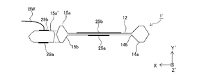
図21は、図1に示した圧電振動素子1の詳細な図であり、同図(a)は斜視図であり、同図(b)は図1(a)におけるQ−Q断面を−Z’軸方向からみた断面図である。図21(a)に示すように、圧電振動素子1のX軸に交わる外形端面には、傾斜面が現出する。つまり、−X軸側の端面には、図21(b)に示すように、傾斜面1(傾斜面a1、a2)が現出し、+X軸側の端面には、傾斜面2(傾斜面b1、b2、b3、b4)が現出している。傾斜面1と傾斜面2のXY’平面に平行な断面形状は、異なっている。
また、傾斜面1、2共に、圧電基板10の主表面と交わる付近には、図19(b)、(e)に示すような+X軸方向に形成される傾斜壁面X2の垂直の壁面は現出していない。この理由は、凹陥部11、11’を形成するのに必要なエッチング時間に比べて、傾斜面1(a1、a2)と傾斜面2の形成時間は、圧電基板(水晶基板)10の外形が貫通するまでエッチングするので、エッチング時間が十分に長いためにオーバーエッチングの作用により、垂直の壁面が現出しないのである。
傾斜面1を構成する傾斜面a1、a2は、X軸に対してほぼ対称関係にあり、傾斜面2を構成する傾斜面b1、b2、b3、b4では、傾斜面b1と傾斜面b4、傾斜面b2と傾斜面b3とが、各々X軸に対してほぼ対称関係にあることが判明した。更に、傾斜面a1、a2のX軸に対する傾斜角度αと、傾斜面b1、b4のX軸に対する傾斜角度βとは、β<αの関係にあることが分かった。
21 is a detailed view of the
Further, in the vicinity where both the
The inclined surfaces a1 and a2 constituting the
図22に示した実施形態例の圧電振動素子1’は、図1に示した圧電振動素子1の変形例であり、第3の厚肉部本体15aの外端部寄りの一部である第3の厚肉部本体15a’の厚みをエッチング等により薄くした構造をしている。この理由は第3の厚肉部本体15a’に形成したパッド電極29bと、外部の電極端子とをボンディングワイヤーBWで接続する際に、ボンディングワイヤーの+Y軸方向における頂点部分が、パッケージに被せる蓋部材に接触しないようにするためである。
The
図1、図5、図6、図7の実施形態例に示すように、高周波の圧電振動素子が小型化されると共に、振動部の支持をする厚肉部が強固であり、振動、衝撃等に強い圧電振動素子が得られるという効果がある。更に、スリットを設けることにより、接着・固定に起因する応力の広がりを抑圧することができるので、周波数温度特性、CI温度特性、及び周波数エージング特性に優れ、且つ主振動のCI値が小さく、主振動のCI値に対する近接したスプリアスのCI値の比、即ちCI値比の大きな圧電振動素子が得られるという効果がある。
また、圧電振動素子を支持する部位が一点になると、導電性接着剤に起因して生じる応力を小さくすることが可能である。
また、図1、図5、図6のように振動部に接してその端部に厚肉部を設けることにより圧電振動素子の耐衝撃性、耐振動性が強化されるという効果がある。
As shown in the embodiments of FIGS. 1, 5, 6, and 7, the high-frequency piezoelectric vibration element is downsized, and the thick-walled portion that supports the vibration portion is strong, and vibration, impact, etc. There is an effect that a strong piezoelectric vibration element can be obtained. Furthermore, by providing a slit, it is possible to suppress the spread of stress due to adhesion / fixing, so that the frequency temperature characteristic, the CI temperature characteristic, and the frequency aging characteristic are excellent, and the CI value of the main vibration is small. There is an effect that a piezoelectric vibration element having a large ratio of the CI value of adjacent spurious to the CI value of vibration, that is, a large CI value ratio can be obtained.
In addition, when the portion that supports the piezoelectric vibration element becomes one point, it is possible to reduce the stress caused by the conductive adhesive.
Also, as shown in FIGS. 1, 5, and 6, there is an effect that the shock resistance and vibration resistance of the piezoelectric vibration element are enhanced by providing a thick portion at the end portion in contact with the vibration portion.
図8、図12、図13の実施形態例に示すように、厚肉部の削減を図ったので、基本波を用いた高周波圧電振動素子の小型化、及び耐衝撃性の強化が図られると共に、量産化が可能となる。更に、支持部と振動領域の間に少なくとも1つのスリットを形成することにより、接着・固定に起因する応力の広がりを抑圧できるので、周波数温度特性、CI温度特性、及び周波数エージング特性に優れた圧電振動素子が得られるという効果がある。 As shown in the embodiment examples of FIGS. 8, 12, and 13, since the thick portion is reduced, the high-frequency piezoelectric vibration element using the fundamental wave can be reduced in size and the impact resistance can be enhanced. Mass production is possible. Furthermore, by forming at least one slit between the support portion and the vibration region, it is possible to suppress the spread of stress due to adhesion and fixation, so that the piezoelectric material has excellent frequency temperature characteristics, CI temperature characteristics, and frequency aging characteristics. There is an effect that a vibration element is obtained.
また、図9の実施形態例に示すように、励振電極25a、25bと、リード電極27a、27b、及びパッド電極29a、29bとは、夫々異種構成の金属材料、即ち励振電極25a、25bはニッケルと金の積層膜で形成され、リード電極27a、27b、及びパッド電極29a、29bはクロムと金の積層膜で形成されている。このようにすることにより、主振動のCI値が小さく、主振動のCI値に対する近接したスプリアスのCI値の比、即ちCI値比の大きな圧電振動素子が得られるという効果がある。
9, the
また、図8、図12、図13の実施形態例に示す圧電振動素子1は、振動部12の他方の主面(裏面)と、第1の厚肉部16の他方の面(裏面)とは、同一平面上にあり、振動部12の一方の主面(表面)と、第2の厚肉部17の他方の面(表面)とは、同一平面上にあるように形成されている。このため、不要な厚肉部を削減しているので、小型化、耐衝撃性の強化に効果がある。さらに、圧電基板10を表裏両面からエッチングして振動領域を形成することにより、エッチングの時間が短縮されるという効果がある。更に、不要の厚肉部を削除することにより小型化が図られると共に、周波数温度特性の優れた、高周波の基本波圧電振動素子が得られるという効果がある。
8, 12, and 13, the
また、図6、図13の実施形態例に示すように、第3の厚肉部15に2つのスリットを設けることにより、圧電振動素子を接着・固定する際に生じる応力の広がりを、よりよく抑圧することができるため、周波数再現性、周波数温度特性、CI温度特性、及び周波数エージング特性に優れ圧電振動素子が得られるという効果がある。
Further, as shown in the embodiment examples of FIGS. 6 and 13, by providing two slits in the third
また、圧電基板10が、図2の切断角度図に示されるように形成されるため、要求仕様の圧電振動素子を、より適したカットアングルで構成することが可能であり、且つ仕様にそった周波数温度特性を有し、CI値が小さく、CI値比の大きな高周波圧電振動素子が得られるという効果がある。
また、圧電基板に回転Yカット水晶基板を用いることにより、フォトリソグラフィー技術及びエッチング技法に関する永年の実績・経験が活用できるので、圧電基板の量産が可能であるのみならず、高精度の圧電基板が得られ、圧電振動素子の歩留りが大幅に改善されるという効果がある。
In addition, since the
In addition, by using a rotating Y-cut quartz substrate as a piezoelectric substrate, many years of experience and experience regarding photolithography and etching techniques can be utilized, so that not only mass production of piezoelectric substrates is possible, but also high-precision piezoelectric substrates As a result, the yield of the piezoelectric vibration element is greatly improved.
また、図1に示すように、第3の厚肉部15が、振動部12と連設した一方の端縁から他方の端縁に向かって離間するにつれて厚みが増加する第3の傾斜部15bと、この第3の傾斜部15bの他方の端縁に連設する第3の厚肉部本体15aと、を有するように構成すれば、高周波で基本波の圧電振動素子が小型化されると共に、振動部の支持が強固であり、振動、衝撃等に強い圧電振動素子が得られるという効果がある。
In addition, as shown in FIG. 1, the third
[振動子]
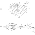
(振動子の形態1)
図23は、本発明に係る振動子の実施形態としての圧電振動子の構成を示す図であり、同図(a)は縦断面図であり、同図(b)は蓋部材を除いた平面図である。圧電振動子50は、例えば上述した第4の実施形態の圧電振動素子4(図23では、圧電振動素子4を用いた例を示したが、他の実施形態にかかる圧電振動素子であってもよい)と、圧電振動素子4を収容するパッケージとを備えている。パッケージは、矩形の箱状に形成されているパッケージ本体40と、金属、セラミック、ガラス等から成る蓋部材49とを含む。
パッケージ本体40は、図23に示すように、第1の基板41と、第2の基板42と、第3の基板43とを積層して形成されており、絶縁材料として、酸化アルミニウム質のセラミック・グリーンシートを成形し、箱状とした後で、焼結して形成される。実装端子45は、第1の基板41の外部底面に複数形成されている。第3の基板43は中央部が除去された環状体であり、第3の基板43の上部周縁に例えばコバール等の金属シールリング44が形成されている。
[Vibrator]
(Form of vibrator 1)
FIG. 23 is a diagram showing a configuration of a piezoelectric vibrator as an embodiment of the vibrator according to the present invention, where FIG. 23 (a) is a longitudinal sectional view and FIG. 23 (b) is a plan view excluding a lid member. FIG. The
As shown in FIG. 23, the
第3の基板43と第2の基板42とにより、圧電振動素子4を収容する凹部(キャビティ)が形成される。第2の基板42の上面の所定の位置には、導体46により実装端子45と電気的に導通する複数の素子搭載パッド47が設けられている。素子搭載パッド47の位置は、圧電振動素子4を載置した際に第3の厚肉部本体15aに形成したパッド電極29aに対応するように配置されている。
パッケージ本体40に圧電振動素子4を固定する際にはまず、圧電振動素子4のパッド電極29aに導電性接着剤30を塗布し、これを反転(裏返し)して素子搭載パッド47に載置して荷重をかける。導電性接着剤30の特性として、導電性接着剤30に起因する応力(∝歪)の大きさは、シリコーン系接着剤、エポキシ系接着剤、ポリイミド系接着剤の順で大きくなる。また、脱ガスは、ポリイミド系接着剤、エポキシ系接着剤、シリコーン系接着剤の順で大きくなる。導電性接着剤30としては経年変化を考慮して脱ガスの少ないポリイミド系接着剤を用いることにした。
The
When the
パッケージ本体40に搭載された圧電振動素子4の導電性接着剤30を硬化させるために、所定の温度の高温炉内に所定の時間入れる。導電性接着剤30を硬化させた後、反転して表面側になったパッド電極29bと、パッケージ本体40の電極端子48とをボンディングワイヤーBWで導通接続する。図23(b)に示すように、圧電振動素子4をパッケージ本体40に支持・固定する部分は、一カ所(1点)、即ち導電性接着剤30だけの一点であるため、支持固定により生じる応力の大きさは小さくすることが可能となる。
アニール処理を施した後、励振電極25bに質量を付加するか、又は質量を減じて周波数調整を行う。パッケージ本体40の上面に形成した金属シールリング44上に、蓋部材49を載置し、真空中か窒素N2ガスの雰囲気中で蓋部材49をシーム溶接して密封する。または、パッケージ本体40の上面に塗布した低融点ガラスに蓋部材49を載置し、溶融して密着する方法もある。パッケージのキャビティ内は真空にするか、又は窒素N2ガス等の不活性ガスで充填して、圧電振動子50が完成する。
In order to cure the
After the annealing treatment, the frequency is adjusted by adding mass to the
なお、圧電振動素子4は、圧電振動素子4を形成する圧電基板の上下面に近接して夫々パッド電極29a、29bを形成している。圧電振動素子4をパッケージ本体40に収容する際に、圧電振動素子4を裏返し、パッド電極29aとパッケージ本体40の素子搭載パッド47とを導電性接着剤30で固定・接続する。表面側になったパッド電極29bと、パッケージの電極端子48とをボンディングワイヤーBWで接続する。このように圧電振動素子4を支持する部位が一点になると、導電性接着剤30に起因して生じる応力を小さくすることが可能である。また、パッケージ本体40に収容するに当たり、圧電振動素子4を裏返して、より大きな励振電極25bを上面にすると、圧電振動素子4の周波数微調が容易となる。
The piezoelectric vibrating
(振動子の形態2)
図24は、振動子の他の実施形態の圧電振動子50’の構成を示す縦断面図である。図23に示した実施形態例と異なる点は、圧電振動素子4の支持の方法である。図23の実施形態例では一カ所支持であるのに対し、図24の実施形態例では圧電振動素子4の一方の面の第3の厚肉部15の2カ所(2点)に導電性接着剤30を塗布して、導通と支持・固定を図るようにした構造である。低背化に適した構造であるが、導電性接着剤30に起因する応力が少し大きくなる虞がある。
(Form of vibrator 2)
FIG. 24 is a longitudinal sectional view showing a configuration of a
そこで、第3、および第6の実施形態である図6、図7や図13、図14に示すようなスリットを2つ設けた圧電振動素子3、7、7’を採用することで、前記応力の振動部への影響を抑圧できることが期待できる。または、導電性接着剤の硬度が比較的硬い場合には、導電性接着剤を塗布する「2カ所(2点)」の中心間距離を狭めることにより、前記2点間で生じる実装に係る歪み(応力)を低減させる手法もある。また一方、導電性接着剤の硬度が比較的柔らかい、シリコーン系接着剤を用いることにより、導電性接着剤に緩衝性を持たせ、前記2点間で生じる実装に係る歪み(応力)を低減させる手法もある。
Therefore, by adopting the piezoelectric vibrating
以上の圧電振動子50,50’の実施形態例では、パッケージ本体40に積層板を用いた例を説明したが、パッケージ本体40に単層セラミック板を用い、蓋体に絞り加工を施したキャップを用いて圧電振動子を構成してもよい。
In the above-described embodiments of the
上述のように、前述の実施形態に示す圧電振動素子4を用いているため、高周波の圧電振動子50、50’が小型化されると共に、耐衝撃性の向上した圧電振動子が得られるという効果がある。さらに、圧電振動素子4を支持する部位が一点であり、且つ被支持部(パッド電極29a)と振動部12との間に少なくとも1つのスリット20を形成することにより導電性接着剤30に起因して生じる応力を小さくすることができる。この結果、周波数再現性、周波数温度特性、CI温度特性、及び周波数エージング特性に優れた圧電振動子が得られるという効果がある。また、主振動のCI値を小さく、主振動のCI値に対する近接したスプリアスのCI値の比、即ちCI値比の大きな圧電振動素子が得られ、且つ容量比γの小さな圧電振動子50、50’が得られるという効果がある。
As described above, since the
また、図24の実施形態例に示すように、二点支持の圧電振動子を構成することにより、低背化した圧電振動子50’を得ることができるという効果がある。スリットを2つ設けることで二点支持に起因した支持応力の振動部への影響を抑圧できる。 Further, as shown in the embodiment of FIG. 24, by configuring a two-point supported piezoelectric vibrator, there is an effect that a piezoelectric vibrator 50 'having a reduced height can be obtained. By providing two slits, it is possible to suppress the influence of the supporting stress caused by the two-point support on the vibration part.
また、図1、及び図3〜6の実施形態例に示すように、励振電極25a、25bの電極材料と、リード電極27a、27b、及びパッド電極29a、29bの電極材料と、を異ならせ、又それらの膜厚も夫々の機能に最適なように構成した圧電振動素子1、2、3を用いているため、主振動のCI値が小さく、主振動のCI値に対する近接したスプリアスのCI値の比、即ちCI値比の大きな圧電振動素子1、2、3が得られるという効果がある。
Further, as shown in the embodiment examples of FIGS. 1 and 3 to 6, the electrode materials of the
[電子デバイスとしての圧電デバイス]
図25は、本発明に係る電子デバイスの実施形態を示す縦断面図である。電子デバイスとしての圧電デバイス60は、第1の実施形態の圧電振動素子1と、電子部品の1つであり、温度センサーとしての感温素子であるサーミスターThと、圧電振動素子1及びサーミスターThを収容するパッケージと、を概略備えている。なお、本例では圧電振動素子1を用いた例を示したが、他の実施形態に示す圧電振動素子であってもよい。
[Piezoelectric devices as electronic devices]
FIG. 25 is a longitudinal sectional view showing an embodiment of an electronic device according to the present invention. A
パッケージは、パッケージ本体40aと、蓋部材49とを備えている。パッケージ本体40aは、上面側に圧電振動素子1を収容するキャビティ31が形成され、外部裏面側にサーミスターThを収容する凹部32が形成されている。キャビティ31の内底面の端部に素子搭載パッド47が設けられ、素子搭載パッド47はパッケージ本体40a内部に配置された導体46で複数の実装端子45と導通接続されている。
圧電振動素子1のパッド電極29aに導電性接着剤30を塗布し、これを反転し、素子搭載パッド47に載置する。反転して表面側になったパッド電極29bと電極端子48とをボンディングワイヤーBWで接続する。パッケージ本体40aの上部には、コバール等からなる金属シールリング44が焼成されており、この金属シールリング44に蓋部材49を載置し、抵抗溶接機等を用いて溶接し、キャビティ31を気密封止する。キャビティ31内は真空にしてもよいし、不活性ガスを封入してもよい。裏面の凹部32の電子部品搭載用パッド33に半田ボール等を用いてサーミスターThの端子を接続して、圧電デバイス60を完成する。
The package includes a package
The
以上の実施形態例では、パッケージ本体40aの外部下面側に凹部32を形成し、電子部品を搭載した例を説明したが、パッケージ本体40aの内部底面に凹部32を形成し、電子部品を搭載してもよい。
また、圧電振動素子1とサーミスターThとをパッケージ本体40aに収容した例を説明したが、パッケージ本体40aに収容する電子部品としては、サーミスター、コンデンサー、リアクタンス素子、半導体素子のうち少なくとも一つを収容して電子デバイスを構成することが望ましい。
In the above embodiment example, the
Moreover, although the example which accommodated the
図25に示す実施形態例は、圧電振動素子1とサーミスターThとをパッケージ本体40aに収容した例である。このように構成すると、感温素子のサーミスターThが圧電振動素子1の極めて近くに位置されているので、圧電振動素子1の温度変化を素早く感知することができるという効果がある。また、本発明にかかる圧電振動素子と上記の電子部品とで電子デバイス(圧電デバイス)を構成することにより、高周波、且つ小型の電子デバイス(圧電デバイス)が構成できるので、多方面の用途に利用できるという効果がある。
また、電子部品に可変容量素子、サーミスター、インダクター、コンデンサーのうちの何れかを用いて電子デバイス(圧電デバイス)を構成すると、要求仕様により適した電子デバイスが、小型で且つ低コストで実現できるという効果がある。
The embodiment shown in FIG. 25 is an example in which the
In addition, when an electronic device (piezoelectric device) is configured by using any one of a variable capacitance element, thermistor, inductor, and capacitor as an electronic component, an electronic device suitable for the required specifications can be realized in a small size and at low cost. There is an effect.
図26は、本発明の実施形態例に係る電子デバイスの一種である圧電発振器70の構成を示す図であって、同図(a)は縦断面図であり、同図(b)は蓋部材を除いた平面図ある。圧電発振器70は、パッケージ本体40b、及び蓋部材49と、第1の実施形態の圧電振動素子1と、圧電振動素子1を励振する発振回路を搭載したIC部品51と、電圧により容量が変化する可変容量素子、温度により抵抗が変化するサーミスター、インダクター等の電子部品52の少なくとも1つと、を備えている。なお、本例では圧電振動素子1を用いた例を示したが、他の実施形態で示した圧電振動素子であってもよい。
FIG. 26 is a diagram showing a configuration of a
圧電振動素子1のパッド電極29aに導電性接着剤(ポリイミド系)30を塗布し、これを反転してパッケージ本体40bの素子搭載パッド47aに載置し、パッド電極29aと素子搭載パッド47aとの導通を図る。反転して上面側になったパッド電極29bと、パッケージ本体40bの他の電極端子48とをボンディングワイヤーBWにて接続し、導通を図る。IC部品51は、パッケージ本体40bの所定の位置に固定し、IC部品51の端子と、パッケージ本体40bの電極端子55とをボンディングワイヤーBWにて接続する。また、電子部品52は、パッケージ本体40bの所定の位置に載置し、金属バンプ等を用いて接続する。パッケージ本体40bを真空、あるいは窒素等の不活性気体で満たし、パッケージ本体40bを蓋部材49で密封して圧電発振器70を完成する。
パッド電極29bとパッケージの電極端子48とをボンディングワイヤーBWで接続する工法は、圧電振動素子1を支持する部位が一点になり、導電性接着剤30に起因して生じる応力を小さくすることが可能である。また、パッケージ本体40bに収容するに当たり、圧電振動素子1を裏返(反転)して、より大きな励振電極25bを上面にしたので、電子デバイスとしての圧電発振器70の周波数微調が容易となる。
A conductive adhesive (polyimide) 30 is applied to the
In the method of connecting the
図26に示した圧電発振器70は、同一のパッケージ本体40bの内部底面上に圧電振動素子1、IC部品51、及び電子部品52を配置したが、図27に示した実施形態の圧電発振器70’は、H型のパッケージ本体40aを用い、上部に形成したキャビティ31に圧電振動素子1を収容し、キャビティ31内部を真空、又は窒素N2ガスで満たし、蓋部材61で密封する。下部には圧電振動素子1を励振する発振回路、増幅回路等を搭載したIC部品51と、可変容量素子、及び必要に応じてインダクター、サーミスター、コンデンサー等の電子部品52と、を金属バンプ(Auバンプ)68を介して、パッケージ本体40aの端子67に導通・接続する。
本実施形態の電子デバイス(圧電発振器)70’は、圧電振動素子1と、IC部品51及び電子部品52とを分離し、圧電振動素子1を単独で気密封止しているために、圧電発振器70の周波数エージングに優れている。
In the
The electronic device (piezoelectric oscillator) 70 ′ of the present embodiment separates the
図26、図27に示すような電子デバイスの一種である圧電発振器70,70’(例えば電圧制御型圧電発振器)を構成することにより、周波数再現性、周波数温度特性、エージング特性が優れ、小型で且つ高周波(例えば490MHz帯)の電圧制御型圧電発振器が得られるという効果がある。また、圧電発振器70,70’は基本波の圧電振動素子1を用いているので、容量比が小さく、基本波圧電振動素子を用いているため周波数可変幅を広く、S/N比の良好な電圧制御型圧電発振器が得られるという効果がある。
また、電子デバイスとして圧電発振器、温度補償型圧電発振器、及び電圧制御型圧電発振器等を構成することが可能であり、周波数再現性、エージング特性が優れた圧電発振器、周波数温度特性に優れた温度補償圧電発振器、周波数が安定で可変範囲の広く且つS/N比(信号雑音比)の良好な電圧制御型圧電発振器を構成することが得られるという効果がある。
By configuring
In addition, it is possible to configure piezoelectric oscillators, temperature compensated piezoelectric oscillators, voltage controlled piezoelectric oscillators, etc. as electronic devices, piezoelectric oscillators with excellent frequency reproducibility and aging characteristics, and temperature compensation with excellent frequency temperature characteristics. The piezoelectric oscillator has an effect that it is possible to obtain a voltage-controlled piezoelectric oscillator having a stable frequency, a wide variable range, and a good S / N ratio (signal to noise ratio).
[電子機器]
図28は本発明の実施形態例に係る電子機器の構成を示す概略構成図である。電子機器8は上述の圧電振動子50、50’を備えている。圧電振動子50を用いた電子機器8としては、伝送機器等が挙げられる。これらの電子機器8において圧電振動子50、50’は、基準信号源、あるいは電圧可変型圧電発振器(VCXO)等として用いられ、小型で、特性の良好な電子機器を提供できる。
本発明にかかる圧電振動子を電子機器に用いることにより、高周波で周波数安定度に優れ、S/N比の良好な基準周波数源を備えた電子機器が構成できるという効果がある。
[Electronics]
FIG. 28 is a schematic configuration diagram showing a configuration of an electronic apparatus according to an embodiment of the present invention. The
By using the piezoelectric vibrator according to the present invention for an electronic device, there is an effect that an electronic device including a reference frequency source having a high frequency and excellent frequency stability and a good S / N ratio can be configured.
次いで、本発明の一実施形態に係る振動素子を適用した電子機器について、図29〜図31に基づき、詳細に説明する。 Next, an electronic device to which the resonator element according to an embodiment of the invention is applied will be described in detail with reference to FIGS.
図29は、本発明の一実施形態に係る振動素子を備える電子機器としてのモバイル型(又はノート型)のパーソナルコンピューターの構成を示す概略斜視図である。この図において、パーソナルコンピューター1100は、キーボード1102を備えた本体部1104と、表示部100を備えた表示ユニット1106とにより構成され、表示ユニット1106は、本体部1104に対しヒンジ構造部を介して回動可能に支持されている。このようなパーソナルコンピューター1100には、フィルター、共振器、基準クロック等として機能する振動素子1が内蔵されている。
FIG. 29 is a schematic perspective view illustrating a configuration of a mobile (or notebook) personal computer as an electronic apparatus including the resonator element according to the embodiment of the invention. In this figure, a
図30は、本発明の一実施形態に係る振動素子を備える電子機器としての携帯電話機(PHSも含む)の構成を示す概略斜視図である。この図において、携帯電話機1200は、複数の操作ボタン1202、受話口1204および送話口1206を備え、操作ボタン1202と受話口1204との間には、表示部100が配置されている。このような携帯電話機1200には、フィルター、共振器等として機能する振動素子1が内蔵されている。
FIG. 30 is a schematic perspective view illustrating a configuration of a mobile phone (including PHS) as an electronic apparatus including the resonator element according to an embodiment of the invention. In this figure, a
図31は、本発明の一実施形態に係る振動素子を備える電子機器としてのデジタルカメラの構成を示す概略斜視図である。なお、この図には、外部機器との接続についても簡易的に示されている。ここで、通常のカメラは、被写体の光像により銀塩写真フィルムを感光するのに対し、デジタルカメラ1300は、被写体の光像をCCD(Charge Coupled Device)等の撮像素子により光電変換して撮像信号(画像信号)を生成する。
デジタルカメラ1300におけるケース(ボディー)1302の背面には、表示部100が設けられ、CCDによる撮像信号に基づいて表示を行う構成になっており、表示部100は、被写体を電子画像として表示するファインダーとして機能する。また、ケース1302の正面側(図中裏面側)には、光学レンズ(撮像光学系)やCCD等を含む受光ユニット1304が設けられている。
撮影者が表示部100に表示された被写体像を確認し、シャッターボタン1306を押下すると、その時点におけるCCDの撮像信号が、メモリー1308に転送・格納される。また、このデジタルカメラ1300においては、ケース1302の側面に、ビデオ信号出力端子1312と、データ通信用の入出力端子1314とが設けられている。そして、図示されるように、ビデオ信号出力端子1312にはテレビモニター1430が、データ通信用の入出力端子1314にはパーソナルコンピューター(PC)1440が、それぞれ必要に応じて接続される。さらに、所定の操作により、メモリー1308に格納された撮像信号が、テレビモニター1430や、パーソナルコンピューター1440に出力される構成になっている。このようなデジタルカメラ1300には、フィルター、共振器等として機能する振動素子1が内蔵されている。
FIG. 31 is a schematic perspective view illustrating a configuration of a digital camera as an electronic apparatus including the resonator element according to an embodiment of the invention. In this figure, connection with an external device is also simply shown. Here, a normal camera sensitizes a silver salt photographic film with a light image of a subject, whereas a
A
When the photographer confirms the subject image displayed on the
なお、本発明の一実施形態に係る振動素子を備える電子機器は、図29のパーソナルコンピューター(モバイル型パーソナルコンピューター)、図30の携帯電話機、図31のデジタルカメラの他にも、例えば、インクジェット式吐出装置(例えばインクジェットプリンター)、ラップトップ型パーソナルコンピューター、テレビ、ビデオカメラ、ビデオテープレコーダー、カーナビゲーション装置、ページャー、電子手帳(通信機能付も含む)、電子辞書、電卓、電子ゲーム機器、ワードプロセッサー、ワークステーション、テレビ電話、防犯用テレビモニター、電子双眼鏡、POS端末、医療機器(例えば電子体温計、血圧計、血糖計、心電図計測装置、超音波診断装置、電子内視鏡)、魚群探知機、各種測定機器、計器類(例えば、車両、航空機、船舶の計器類)、フライトシミュレーター等に適用することができる。 The electronic device including the vibration element according to the embodiment of the present invention includes, for example, an ink jet type in addition to the personal computer (mobile personal computer) in FIG. 29, the mobile phone in FIG. 30, and the digital camera in FIG. Discharge device (for example, inkjet printer), laptop personal computer, TV, video camera, video tape recorder, car navigation device, pager, electronic notebook (including communication function), electronic dictionary, calculator, electronic game device, word processor, Workstations, videophones, crime prevention TV monitors, electronic binoculars, POS terminals, medical equipment (for example, electronic thermometers, blood pressure monitors, blood glucose meters, electrocardiogram measuring devices, ultrasonic diagnostic devices, electronic endoscopes), fish detectors, various types Measuring equipment, instruments (eg cars , Aircraft, gauges of a ship), can be applied to a flight simulator or the like.
[移動体]
図32は移動体の一例としての自動車を概略的に示す斜視図である。自動車106には上述の振動素子を有する振動子や電子デバイスが搭載されている。例えば、キーレスエントリー、イモビライザー、カーナビゲーションシステム、カーエアコン、アンチロックブレーキシステム(ABS)、エアーバック、タイヤ・プレッシャー・モニタリング・システム(TPMS:Tire Pressure Monitoring System)、エンジンコントロール、ハイブリッド自動車や電気自動車の電池モニター、車体姿勢制御システム、等の電子制御ユニット(ECU:electronic control unit)に広く適用できる。
[Moving object]
FIG. 32 is a perspective view schematically showing an automobile as an example of a moving body. The
[変形実施形態:その1]
圧電振動素子の実装に起因した応力を更に軽減、抑圧する手法として、以下に示すごとき構造を採用することができる。
図33(a)の圧電基板10は、振動部12を有する薄肉部と、当該薄肉部の周縁に設けられ、当該薄肉部よりも厚い厚肉部13とを備えている。厚肉部13の内の一つの厚肉部分には、振動部12に沿ってスリット20が設けられており、縁辺の方向に緩衝部Sを介してマウント部Fが横並びで接続されている。マウント部Fは、マウント部Fと緩衝部Sと厚肉部13との並ぶ方向に対して直交方向の両端部に、面取り部21を有している。
[Modified Embodiment: Part 1]
As a technique for further reducing and suppressing the stress caused by mounting the piezoelectric vibration element, the following structure can be adopted.
The
図33(b)の圧電基板10は、振動部12を有する薄肉部と、当該薄肉部の周縁に設けられ、当該薄肉部よりも厚い厚肉部13とを備えている。厚肉部13の内の一つの厚肉部分には、振動部12に沿ってスリット20が設けられており、縁辺の方向に緩衝部Sを介してマウント部Fが横並びで接続されている。マウント部Fは、マウント部Fと緩衝部Sと厚肉部13との並ぶ方向に対して直交方向の両端部に切欠き部22を有している。スリット20の長手方向は、前記直交方向と略平行であり、マウント部Fの直交方向の幅を、スリット20の長手方向の幅より狭く形成されている。更に、スリット20の長手方向の両端部は、マウント部Fの両端部よりも前記直交方向の外周寄りにある。
The
図33(c)の圧電基板10は、振動部12を有する薄肉部と、当該薄肉部の周縁に設けられ、当該薄肉部よりも厚い厚肉部13とを備えている。厚肉部13の内の一つの厚肉部分には、振動部12に沿ってスリット20が設けられており、縁辺の方向に緩衝部Sとマウント部Fとが横並びで連結されている。マウント部Fは、マウント部Fと緩衝部Sと厚肉部13との並ぶ方向に対して直交方向の両端部に、切欠き部22を有している。スリット20と緩衝部Sとが設けられている厚肉部分は、マウント部Fと緩衝部Sとの並ぶ方向に対して直交方向の端部が、振動部12の端部および当該厚肉部分の延在方向に対して直交方向に設けられている他の厚肉部分の端部よりも突出している。
The
図34は、図33の構造に対し、2点支持の形態、即ちマウント部Fに換えてマウント部F1、マウント部F2の形態をとることを特徴としている。
なお、図33、図34においては、厚肉部13の各厚肉部(第1の厚肉部16、第3の厚肉部15、第4の厚肉部14)の内壁に傾斜部が図示されている一方で、また厚肉部13の外側の側壁面には図21に示した如き傾斜面が図示されていないが、これらの傾斜部、傾斜面は図21に示しているように対応する部位に形成されることになる。
なお、図33、図34中の各符号は、上記各実施形態の同じ符号が示す部位と対応している。
FIG. 34 is characterized in that the structure of FIG. 33 is in the form of two-point support, that is, in the form of a mount part F1 and a mount part F2 instead of the mount part F.
In FIGS. 33 and 34, there is an inclined portion on the inner wall of each thick portion of the thick portion 13 (the first
In addition, each code | symbol in FIG. 33, FIG. 34 respond | corresponds with the site | part which the same code | symbol of said each embodiment shows.
[変形実施形態:その2]
図35は圧電振動素子1の変形例であり、同図(a)は平面図、同図(b)は圧電振動素子1のパッド電極29a(マウント部F)の拡大図平面図を示し、同図(c)はマウント部Fの断面図を示している。このマウント部Fにおいては、接着強度を向上させるために表面上を凹凸状とすることによって接着する面積を拡げている。
[Modified Embodiment: Part 2]
FIG. 35 is a modified example of the
1,1’,2,3,4,6,7…圧電振動素子、8…電子機器、10…圧電基板、10W…水晶ウェハー、11,11’…凹陥部、12…振動部、12a,12b,12c,12d…振動部の一辺、13…厚肉部、14…第4の厚肉部、14a…第4の厚肉部本体、14b…第4の傾斜部、15…第3の厚肉部、15a…第3の厚肉部本体、15b…第3の傾斜部、15b’,15bb…極細の傾斜部、16…第1の厚肉部、16a…第1の厚肉部本体、16b…第1の傾斜部、17…第2の厚肉部、17a…第2の厚肉部本体、17b…第2の傾斜部、20…スリット、20a…第1のスリット、20b…第2のスリット、21…面取り部、22…切欠き部、25a,25b…励振電極、27a,27b…リード電極、29a,29b…パッド電極、30…導電性接着剤、31…キャビティ、32…凹部、33…電子部品搭載用パッド、40,40a,40b…パッケージ本体、41…第1の基板、42…第2の基板、43…第3の基板、44…金属シールリング、45…実装端子、46…導体、47…素子搭載パッド、48…電極端子、49…蓋部材、50、50’…圧電振動子、51…IC部品、52電子部品、55…電極端子、60、70…圧電デバイス、61…蓋部材、65…実装端子、66…導体、67…部品端子、68…金属バンプ(Auバンプ)、Th…サーミスター、F、F1、F2…マウント部、S…緩衝部。
DESCRIPTION OF
Claims (20)
前記振動部の第1の外縁に沿って前記振動部と一体的に設けられ、前記振動部よりも厚みが厚い第1の厚肉部と、
前記第1の外縁と対峙する前記振動部の第2の外縁に沿って前記振動部と一体的に設けられ、前記振動部よりも厚みが厚い第2の厚肉部と
を含む基板を備え、
前記第1の厚肉部は、前記振動部の一方の主面よりも突出して設けられ、
前記第2の厚肉部は、前記振動部の一方の主面に対する裏側の主面よりも突出して設けられていることを特徴とする振動素子。 A vibrating part;
A first thick portion provided integrally with the vibrating portion along a first outer edge of the vibrating portion, and having a thickness greater than the vibrating portion;
A substrate including a second thick portion provided integrally with the vibrating portion along a second outer edge of the vibrating portion facing the first outer edge, and having a thickness greater than the vibrating portion;
The first thick part is provided to protrude from one main surface of the vibration part,
The vibration element according to claim 1, wherein the second thick portion is provided so as to protrude from a main surface on the back side with respect to one main surface of the vibration portion.
前記第1の外縁及び前記第2の外縁のそれぞれの一方の端部の間を結んでいる前記振動部の第3の外縁に沿って、前記振動部と一体的に、前記振動部よりも厚みが厚い第3の厚肉部が設けられていることを特徴とする振動素子。 In claim 1,
Along with the third outer edge of the vibration part connecting between one end of each of the first outer edge and the second outer edge, the thickness is larger than the vibration part integrally with the vibration part. A vibration element characterized in that a thick third portion is provided.
前記第1の外縁及び前記第2の外縁のそれぞれの他方の端部の間を結んでいる前記振動部の第4の外縁に沿って、前記振動部と一体的に、前記振動部よりも厚みが厚い第4の厚肉部が設けられていることを特徴とする振動素子。 In claim 2,
Along with the fourth outer edge of the vibrating part connecting the other end of each of the first outer edge and the second outer edge, the thickness of the vibrating part is integrated with the vibrating part. A vibration element, characterized in that a thick fourth portion is provided.
前記基板は、回転Yカット水晶基板であることを特徴とする振動素子。 In any one of Claims 1 thru | or 3,
The vibrating element according to claim 1, wherein the substrate is a rotating Y-cut quartz substrate.
前記第3の厚肉部は、前記振動部を基準にして平面視で、+X軸側にあることを特徴とする振動素子。 In claim 4,
The vibration element according to claim 3, wherein the third thick part is on the + X axis side in a plan view with respect to the vibration part.
前記第4の厚肉部は、前記振動部を基準にして平面視で、−X軸側にあることを特徴とする振動素子。 In claim 5,
The vibration element according to claim 4, wherein the fourth thick part is on the −X axis side in a plan view with respect to the vibration part.
前記第3の厚肉部は、前記振動部と連設している一方の端縁から他方の端縁に向かって離間するにつれて厚みが増加している傾斜部と、
当該傾斜部の前記他方の端縁に連設する厚肉部本体と、を含むことを特徴とする振動素子。 In claim 5 or 6,
The third thick part is an inclined part that increases in thickness as it is separated from one end edge connected to the vibration part toward the other end edge;
A vibration element comprising: a thick portion main body provided continuously with the other edge of the inclined portion.
前記第3の厚肉部には、少なくとも一つのスリットが設けられていることを特徴とする振動素子。 In claim 7,
The vibration element, wherein the third thick part is provided with at least one slit.
前記スリットは、前記傾斜部と前記厚肉部本体との境界部に沿って前記厚肉部本体に設けられていることを特徴とする振動素子。 In claim 8,
The vibration element according to claim 1, wherein the slit is provided in the thick portion main body along a boundary portion between the inclined portion and the thick portion main body.
前記スリットは、前記傾斜部内に前記振動部の前記第3の外縁から離間して配置されていることを特徴とする振動素子。 In claim 8,
The vibration element according to claim 1, wherein the slit is disposed in the inclined portion so as to be separated from the third outer edge of the vibration portion.
前記スリットは、
前記厚肉部本体に配置されている第1のスリットと、
前記傾斜部内に前記振動部の前記第3の外縁から離間して配置されている第2のスリットと、を含むことを特徴とする振動素子。 In claim 8,
The slit is
A first slit disposed in the thick part body;
And a second slit disposed in the inclined portion so as to be separated from the third outer edge of the vibration portion.
前記第1のスリットは、
前記傾斜部と前記厚肉部本体との前記境界部に沿って前記厚肉部本体に配置されていることを特徴とする振動素子。 In claim 11,
The first slit is
The vibration element is arranged in the thick part main body along the boundary part between the inclined part and the thick part main body.
前記振動素子を収容するパッケージと、を備えていることを特徴とする振動子。 The vibration element according to any one of claims 1 to 3,
And a package for housing the vibration element.
電子部品と、をパッケージに備えていることを特徴とする電子デバイス。 The vibration element according to any one of claims 1 to 3,
An electronic device comprising an electronic component and a package.
前記電子部品は、可変容量素子、サーミスター、インダクター及びコンデンサーの少なくとも何れかであることを特徴とする電子デバイス。 In claim 14,
The electronic device is at least one of a variable capacitance element, a thermistor, an inductor, and a capacitor.
前記振動素子を励振する発振回路と、をパッケージに備えていることを特徴とする電子デバイス。 The vibration element according to any one of claims 1 to 3,
An electronic device comprising: an oscillation circuit that excites the vibration element; and a package.
基板を準備する工程と、
前記基板エッチング加工することによって前記第1の厚肉部及び前記第2の厚肉部を形成する厚肉部形成工程と、
前記基板をエッチング加工することによって前記振動素子の外形を形成する振動素子外形形成工程と、
前記振動素子に電極を形成する電極形成工程と、を含むことを特徴とする振動素子の製造方法。 The vibration part is provided integrally with the vibration part along the first outer edge and the second outer edge of the vibration part facing each other, protrudes from one main surface of the vibration part, and is thicker than the vibration part. A vibration element manufacturing method comprising: a thick first thick portion; and a second thick portion that protrudes from a main surface on the back side with respect to one main surface of the vibration portion and is thicker than the vibration portion. And
Preparing a substrate;
A thick part forming step of forming the first thick part and the second thick part by etching the substrate;
A vibrating element outer shape forming step of forming an outer shape of the vibrating element by etching the substrate;
And an electrode forming step of forming an electrode on the vibration element.
Priority Applications (4)
| Application Number | Priority Date | Filing Date | Title |
|---|---|---|---|
| JP2012131639A JP2013258452A (en) | 2012-06-11 | 2012-06-11 | Vibration element, vibrator, electronic device, electronic apparatus, mobile body, and manufacturing method of vibration element |
| CN201210291072.7A CN102957394B (en) | 2011-08-18 | 2012-08-15 | The manufacture method of vibrating elements, oscillator, electronic installation, electronic equipment, moving body and vibrating elements |
| US13/587,252 US8791766B2 (en) | 2011-08-18 | 2012-08-16 | Resonating element, resonator, electronic device, electronic apparatus, moving vehicle, and method of manufacturing resonating element |
| US14/312,060 US20140300252A1 (en) | 2011-08-18 | 2014-06-23 | Resonating element, resonator, electronic device, electronic apparatus, moving vehicle and method of manufacturing resonating element |
Applications Claiming Priority (1)
| Application Number | Priority Date | Filing Date | Title |
|---|---|---|---|
| JP2012131639A JP2013258452A (en) | 2012-06-11 | 2012-06-11 | Vibration element, vibrator, electronic device, electronic apparatus, mobile body, and manufacturing method of vibration element |
Publications (2)
| Publication Number | Publication Date |
|---|---|
| JP2013258452A true JP2013258452A (en) | 2013-12-26 |
| JP2013258452A5 JP2013258452A5 (en) | 2015-07-09 |
Family
ID=49954573
Family Applications (1)
| Application Number | Title | Priority Date | Filing Date |
|---|---|---|---|
| JP2012131639A Withdrawn JP2013258452A (en) | 2011-08-18 | 2012-06-11 | Vibration element, vibrator, electronic device, electronic apparatus, mobile body, and manufacturing method of vibration element |
Country Status (1)
| Country | Link |
|---|---|
| JP (1) | JP2013258452A (en) |
Cited By (3)
| Publication number | Priority date | Publication date | Assignee | Title |
|---|---|---|---|---|
| JP2016174328A (en) * | 2015-03-18 | 2016-09-29 | セイコーエプソン株式会社 | Wafer manufacturing method and wafer |
| JP2020182054A (en) * | 2019-04-24 | 2020-11-05 | 京セラ株式会社 | Piezoelectric piece for vibration element, piezoelectric vibration element, and piezoelectric device |
| JP7465454B2 (en) | 2019-12-27 | 2024-04-11 | 株式会社村田製作所 | Piezoelectric vibration element, piezoelectric vibrator and electronic device |
Citations (10)
| Publication number | Priority date | Publication date | Assignee | Title |
|---|---|---|---|---|
| JP2000013176A (en) * | 1998-06-25 | 2000-01-14 | Victor Co Of Japan Ltd | Oscillator for digital temperature control oscillator |
| JP2002033640A (en) * | 2000-07-17 | 2002-01-31 | Toyo Commun Equip Co Ltd | Piezoelectric device |
| JP2002374146A (en) * | 2001-06-13 | 2002-12-26 | Seiko Epson Corp | Piezoelectric vibrating reed and piezoelectric device |
| JP2005020141A (en) * | 2003-06-24 | 2005-01-20 | Seiko Epson Corp | Manufacturing method of piezoelectric vibration chip and manufacturing method of piezoelectric device |
| JP2005033293A (en) * | 2003-07-08 | 2005-02-03 | Toyo Commun Equip Co Ltd | Piezoelectric device |
| JP2005303825A (en) * | 2004-04-14 | 2005-10-27 | Daishinku Corp | Crystal filter |
| JP2007201858A (en) * | 2006-01-27 | 2007-08-09 | Epson Toyocom Corp | Crystal resonator, and highly accurate crystal oscillator |
| JP2009159000A (en) * | 2007-12-25 | 2009-07-16 | Epson Toyocom Corp | Inverted mesa shaped piezoelectric vibrating reed, inverted mesa shaped piezoelectric device and method of manufacturing inverted mesa shaped piezoelectric device |
| JP2011109681A (en) * | 2000-12-12 | 2011-06-02 | Epson Toyocom Corp | Surface mounted piezoelectric device |
| JP2012029262A (en) * | 2010-07-28 | 2012-02-09 | Seiko Epson Corp | Piezoelectric vibration piece and method of manufacturing the same |
-
2012
- 2012-06-11 JP JP2012131639A patent/JP2013258452A/en not_active Withdrawn
Patent Citations (10)
| Publication number | Priority date | Publication date | Assignee | Title |
|---|---|---|---|---|
| JP2000013176A (en) * | 1998-06-25 | 2000-01-14 | Victor Co Of Japan Ltd | Oscillator for digital temperature control oscillator |
| JP2002033640A (en) * | 2000-07-17 | 2002-01-31 | Toyo Commun Equip Co Ltd | Piezoelectric device |
| JP2011109681A (en) * | 2000-12-12 | 2011-06-02 | Epson Toyocom Corp | Surface mounted piezoelectric device |
| JP2002374146A (en) * | 2001-06-13 | 2002-12-26 | Seiko Epson Corp | Piezoelectric vibrating reed and piezoelectric device |
| JP2005020141A (en) * | 2003-06-24 | 2005-01-20 | Seiko Epson Corp | Manufacturing method of piezoelectric vibration chip and manufacturing method of piezoelectric device |
| JP2005033293A (en) * | 2003-07-08 | 2005-02-03 | Toyo Commun Equip Co Ltd | Piezoelectric device |
| JP2005303825A (en) * | 2004-04-14 | 2005-10-27 | Daishinku Corp | Crystal filter |
| JP2007201858A (en) * | 2006-01-27 | 2007-08-09 | Epson Toyocom Corp | Crystal resonator, and highly accurate crystal oscillator |
| JP2009159000A (en) * | 2007-12-25 | 2009-07-16 | Epson Toyocom Corp | Inverted mesa shaped piezoelectric vibrating reed, inverted mesa shaped piezoelectric device and method of manufacturing inverted mesa shaped piezoelectric device |
| JP2012029262A (en) * | 2010-07-28 | 2012-02-09 | Seiko Epson Corp | Piezoelectric vibration piece and method of manufacturing the same |
Cited By (4)
| Publication number | Priority date | Publication date | Assignee | Title |
|---|---|---|---|---|
| JP2016174328A (en) * | 2015-03-18 | 2016-09-29 | セイコーエプソン株式会社 | Wafer manufacturing method and wafer |
| JP2020182054A (en) * | 2019-04-24 | 2020-11-05 | 京セラ株式会社 | Piezoelectric piece for vibration element, piezoelectric vibration element, and piezoelectric device |
| JP7256680B2 (en) | 2019-04-24 | 2023-04-12 | 京セラ株式会社 | Piezoelectric piece for vibration element, piezoelectric vibration element and piezoelectric device |
| JP7465454B2 (en) | 2019-12-27 | 2024-04-11 | 株式会社村田製作所 | Piezoelectric vibration element, piezoelectric vibrator and electronic device |
Similar Documents
| Publication | Publication Date | Title |
|---|---|---|
| US8791766B2 (en) | Resonating element, resonator, electronic device, electronic apparatus, moving vehicle, and method of manufacturing resonating element | |
| JP6175743B2 (en) | Manufacturing method of vibration element | |
| US9013242B2 (en) | Resonator element, resonator, electronic device, electronic apparatus, and mobile object | |
| JP2013258571A (en) | Vibration element, vibrator, electronic device, electronic apparatus, and moving body | |
| US20160028369A1 (en) | Resonator element, resonator, oscillator, electronic apparatus, and mobile object | |
| US9748920B2 (en) | Resonator element, resonator, electronic device, electronic apparatus, and moving object | |
| JP5824967B2 (en) | Vibration element, vibrator, electronic device, and electronic apparatus | |
| JP6079280B2 (en) | Vibration element, vibrator, electronic device, electronic device, and moving object | |
| JP2013255051A (en) | Vibration element, vibrator, electronic device, electronic apparatus and manufacturing method of vibration element | |
| JP2014007693A (en) | Vibration element, vibrator, electronic device, electronic apparatus, and mobile body | |
| JP6191152B2 (en) | Vibration element, vibrator, electronic device, electronic device, and moving object | |
| JP6064350B2 (en) | Vibration element, vibrator, electronic device, and electronic apparatus | |
| JP2013042440A (en) | Piezoelectric vibrating element, piezoelectric vibrator, electronic device and electronic apparatus | |
| JP5910092B2 (en) | Piezoelectric vibration element, piezoelectric vibrator, electronic device, and electronic apparatus | |
| JP5824958B2 (en) | Vibration element, vibrator, electronic device, and electronic apparatus | |
| JP2013046085A (en) | Piezoelectric vibration element, piezoelectric vibrator, electronic device, and electronic device | |
| JP6561447B2 (en) | Vibrator, oscillator, electronic device, and moving object | |
| JP6074903B2 (en) | Vibration element, vibrator, electronic device, and electronic apparatus | |
| JP2013258452A (en) | Vibration element, vibrator, electronic device, electronic apparatus, mobile body, and manufacturing method of vibration element | |
| JP2020025344A (en) | Vibration element, vibrator, electronic device, electronic apparatus, mobile body, and manufacturing method of vibration element | |
| JP6303372B2 (en) | Vibration element, vibrator, electronic device, electronic device, and moving object | |
| JP2014023015A (en) | Vibration element, vibrator, electronic device, electronic apparatus, and movable body | |
| JP6627902B2 (en) | Vibrating element, vibrator, electronic device, electronic apparatus, moving body, and method of manufacturing vibrating element | |
| JP6562101B2 (en) | Vibration element, vibrator, electronic device, electronic device, and moving object | |
| JP6137274B2 (en) | Vibration element, vibrator, electronic device, and electronic apparatus |
Legal Events
| Date | Code | Title | Description |
|---|---|---|---|
| RD04 | Notification of resignation of power of attorney |
Free format text: JAPANESE INTERMEDIATE CODE: A7424 Effective date: 20150108 |
|
| A521 | Request for written amendment filed |
Free format text: JAPANESE INTERMEDIATE CODE: A523 Effective date: 20150525 |
|
| A621 | Written request for application examination |
Free format text: JAPANESE INTERMEDIATE CODE: A621 Effective date: 20150525 |
|
| A977 | Report on retrieval |
Free format text: JAPANESE INTERMEDIATE CODE: A971007 Effective date: 20160311 |
|
| A131 | Notification of reasons for refusal |
Free format text: JAPANESE INTERMEDIATE CODE: A131 Effective date: 20160322 |
|
| A761 | Written withdrawal of application |
Free format text: JAPANESE INTERMEDIATE CODE: A761 Effective date: 20160513 |