JP6137274B2 - Vibration element, vibrator, electronic device, and electronic apparatus - Google Patents
Vibration element, vibrator, electronic device, and electronic apparatus Download PDFInfo
- Publication number
- JP6137274B2 JP6137274B2 JP2015217344A JP2015217344A JP6137274B2 JP 6137274 B2 JP6137274 B2 JP 6137274B2 JP 2015217344 A JP2015217344 A JP 2015217344A JP 2015217344 A JP2015217344 A JP 2015217344A JP 6137274 B2 JP6137274 B2 JP 6137274B2
- Authority
- JP
- Japan
- Prior art keywords
- axis
- piezoelectric
- region
- vibration element
- main surface
- Prior art date
- Legal status (The legal status is an assumption and is not a legal conclusion. Google has not performed a legal analysis and makes no representation as to the accuracy of the status listed.)
- Active
Links
Images


Description
本発明は、厚みすべり振動モードを励振する圧電振動子に関し、特に所謂逆メサ型構造を有する圧電振動素子、圧電振動子、電子デバイス、及び圧電振動子を用いた電子機器に関する。 The present invention relates to a piezoelectric vibrator that excites a thickness shear vibration mode, and more particularly, to a piezoelectric vibration element, a piezoelectric vibrator, an electronic device, and an electronic device using the piezoelectric vibrator having a so-called inverted mesa structure.
ATカット水晶振動子は、励振する主振動の振動モードが厚みすべり振動であり、小型化、高周波数化に適し、且つ周波数温度特性が優れた三次曲線を呈するので、圧電発振器、電子機器等の多方面で使用されている。
特許文献1には、主面の一部に凹陥部を形成して高周波化を図った所謂逆メサ構造のATカット水晶振動子が開示されている。水晶基板のZ’軸方向の長さが、X軸方向の長さより長い、所謂Z’ロング基板を用いている。
特許文献2には、矩形状の薄肉の振動部の三辺に各々厚肉の支持部が連設され、前記薄肉の振動部の一辺が露出した構造を有する逆メサ構造のATカット水晶振動子が開示されている。更に、水晶振動片は、ATカット水晶基板のX軸とZ’軸を、夫々Y’軸を中心に−120°〜+60°の範囲で回転させてなる面内回転ATカット水晶基板であり、振動領域を確保し、且つ量産性に優れた(多数個取り)構造であるという。
AT-cut quartz resonators have thickness shear vibration as the main vibration mode to be excited, and are suitable for miniaturization and higher frequency, and exhibit a cubic curve with excellent frequency temperature characteristics. Used in many ways.
特許文献3、4には、矩形状の薄肉の振動部の三辺に各々厚肉の支持部が連設され、前記薄肉の振動部の一辺が露出した構造を有する逆メサ構造のATカット水晶振動子が開示されており、水晶振動片は水晶基板のX軸方向の長さがZ’軸方向の長さより長い、所謂Xロング基板が用いられている。
特許文献5には、矩形状の薄肉の振動部の隣接する二辺に各々厚肉の支持部が連設され、平面視でL字状に厚肉部が設けられ、前記薄肉の振動部の二辺が露出した構造を有する逆メサ構造のATカット水晶振動子が開示されている。水晶基板にはZ’ロング基板が用いられている。
しかしながら、特許文献5においては、L字状の厚肉部を得るために、特許文献5の図1(c)、(d)に記載されているように線分αと、線分βに沿って厚肉部を削除しているが、当該削除はダイシング等の機械加工で削除することを前提としているため、切断面にチッピングやクラック等のダメージを負い、超薄部が破損してしまう問題がある。また、振動領域にスプリアスの原因となる不要振動の発生やCI値の増加等の問題が発生する。
特許文献6には、薄肉の振動部の一辺のみに厚肉の支持部が連設され前記薄肉の振動部の三辺が露出した構造を有する逆メサ構造のATカット水晶振動子が開示されている。
In
In
However, in
特許文献7には、水晶基板の両主面であって表裏面で対向するように凹陥部を形成することにより、高周波化を図った逆メサ構造のATカット振動子が開示されている。水晶基板にはXロング基板が用いられ、凹陥部に形成された振動領域の平坦性が確保された領域に励振電極が設けられ構造が提案されている。
ところで、ATカット水晶振動子の振動領域に励振される厚み滑り振動モードは、弾性定数の異方性により振動変位分布がX軸方向に長径を有する楕円状になることが知られている。特許文献8には、圧電基板の表裏両面に表裏対称に配置された一対のリング状電極を有する厚みすべり振動を励振する圧電振動子が開示されている。リング状電極が対称零次モードのみを励起し、それ以外の非調和高次モードをほとんど励起しないように、リング状電極の外周の径と内周の径との差を設定したものである。
By the way, it is known that the thickness-shear vibration mode excited in the vibration region of the AT-cut crystal resonator has an elliptical shape in which the vibration displacement distribution has a major axis in the X-axis direction due to the anisotropy of the elastic constant.
特許文献9には、圧電基板、及び圧電基板の表裏に設ける励振電極の形状を、共に長円形状にした圧電振動子が開示されている。
特許文献10には、水晶基板の長手方向(X軸方向)の両端部、及び電極のX軸方向の両端部の形状を共に半楕円状とし、且つ楕円の長軸対短軸の比(長軸/短軸)を、ほぼ1.26とした水晶振動子が開示されている。
特許文献11には、楕円の水晶基板上に楕円の励振電極を形成した水晶振動子が開示されている。長軸対短軸の比は、1.26:1が望ましいが、製造寸法のバラツキ等を考慮すると、1.14〜1.39:1の範囲程度が実用的であるという。
Patent Document 9 discloses a piezoelectric vibrator in which the shape of a piezoelectric substrate and excitation electrodes provided on the front and back surfaces of the piezoelectric substrate are both elliptical.
特許文献12には、厚みすべり圧電振動子のエネルギー閉じ込め効果をより改善するために、振動部と支持部との間に切り欠きやスリットを設けた構造の圧電振動子が開示されている。
ところで、圧電振動子の小型化を図る際に、接着剤に起因する残留応力により、電気的特性の劣化や周波数エージング特性に不良が生じることがある。特許文献13には、矩形平板状のATカット水晶振動子の振動部と支持部との間に、切り欠きやスリットを設けた水晶振動子が開示されている。このような構造を用いることにより、残留応力が振動領域へ広がるのを抑制できるという。
特許文献14には、マウント歪(応力)を改善(緩和)するために、逆メサ型圧電振動子の振動部と支持部との間に切り欠きやスリットを設けた振動子が開示されている。特許文献15には、逆メサ型圧電振動子の支持部にスリット(貫通孔)を設けることにより、表裏面の電極の導通を確保した圧電振動子が開示されている。
By the way, when the piezoelectric vibrator is miniaturized, there is a case where the electrical characteristics are deteriorated or the frequency aging characteristics are deteriorated due to the residual stress caused by the adhesive.
特許文献16には、厚みすべり振動モードのATカット水晶振動子の支持部に、スリットを設けることにより、高次輪郭系の不要モードを抑圧した水晶振動子が開示されている。
また、特許文献17には、逆メサ型ATカット水晶振動子の薄肉の振動部と、厚肉の保持部との連設部、即ち傾斜面を有する残渣部に、スリットを設けることにより、スプリアスを抑圧する振動子が開示されている。
Further, in
近年、圧電デバイスの小型化、高周波化、並びに高性能化に対する要求は強い。しかしながら、小型化、高周波化を図ろうとすると、前述のごとき構造の圧電振動子は、主振動のCI値、近接するスプリアスのCI値比(=CIs/CIm、ここでCImは主振動のCI値、CIsはスプリアスのCI値で、規格の1例は1.8以上)等が要求を満たせないという問題があることが判明した。特に、周波数が数百MHzという高周波になると、圧電振動素子に形成する励振電極、及びリード電極の電極膜厚が問題になる。圧電振動素子の主振動のみを閉じ込めモードにしようとすると、電極膜が薄くなり、オーミックロスが生じ、圧電振動素子のCI値が大きくなるという問題があった。
また、電極膜のオーミックロスを防ぐために膜厚を厚くすると、主振動の他に多くのインハーモニック・モードが閉じ込めモードとなり、近接するスプリアスCI値比を満たせないという問題があった。
そこで、本発明は上記問題を解決するためになされたもので、高周波化(100〜500MHz帯)を図ると共に、主振動のCI値を低減し、スプリアスCI値比等の電気的要求を満たした圧電振動素子、圧電振動子、電子デバイス、及び本発明の圧電振動子を用いた電子機器を提供することにある。
In recent years, there has been a strong demand for miniaturization, high frequency, and high performance of piezoelectric devices. However, in order to reduce the size and increase the frequency, the piezoelectric vibrator having the structure as described above has the CI value of the main vibration and the CI value ratio of adjacent spurious (= CIs / CIm, where CIm is the CI value of the main vibration. CIs is a CI value of spurious, and one example of the standard is 1.8 or more), etc. In particular, when the frequency is as high as several hundred MHz, the film thickness of the excitation electrode and the lead electrode formed on the piezoelectric vibration element becomes a problem. When only the main vibration of the piezoelectric vibration element is set to the confinement mode, there is a problem that the electrode film becomes thin, ohmic cross occurs, and the CI value of the piezoelectric vibration element increases.
In addition, when the film thickness is increased in order to prevent ohmic crossing of the electrode film, there is a problem in that many in-harmonic modes other than the main vibration become a confinement mode and the adjacent spurious CI value ratio cannot be satisfied.
Therefore, the present invention has been made to solve the above-described problem, and has achieved high frequency (100 to 500 MHz band), reduced the CI value of the main vibration, and satisfied electrical requirements such as a spurious CI value ratio. It is an object of the present invention to provide a piezoelectric vibration element, a piezoelectric vibrator, an electronic device, and an electronic apparatus using the piezoelectric vibrator of the present invention.
本発明は、上記の課題の少なくとも一部を解決するためになされたものであり、以下の形態または適用例として実現することが可能である。
本発明のある形態に係る振動素子は、XYZ直交座標系におけるX軸方向およびZ軸方向に沿った面とY軸方向に沿った厚みを有し、振動領域を含む第1領域、および前記第1領域よりも厚みが厚い第2領域を含む基板と、前記基板の一方の主面側であって前記第1領域に設けられている第1の励振電極と、前記基板の他方の主面側であって前記第1領域に設けられている第2の励振電極と、を備え、前記第1領域は、前記Z軸方向に沿った第1外縁および第2外縁と、前記X軸方向に沿った第3外縁および第4外縁と、を含み、前記第2領域は、前記第1外縁に沿って設けられている第1の肉厚部本体、および前記第1外縁と前記第1の肉厚部本体との間に設けられ前記第1外縁から前記第1の肉厚部本体に向かって厚さが増加している第1の傾斜部を有している第1の肉厚部と、前記第3外縁に沿って設けられている第2の肉厚部本体、および前記第3外縁と前記第2の肉厚部本体との間に設けられ前記第3外縁から前記第2の肉厚部本体に向かって厚さが増加している第2の傾斜部を有している第2の肉厚部と、を含み、前記第1の肉厚部は、前記一方の主面側に設けられ前記第1の励振電極に接続している第1のパッド電極、および前記他方の主面側に設けられ平面視で前記第1のパッド電極と重なっており前記第2の励振電極に接続している第2のパッド電極を備え、前記第1の励振電極は、前記X軸方向に沿っている第5外縁および第6外縁を含み、前記第1のパッド電極は、平面視で、前記第5外縁を通り前記X軸方向に沿った第1仮想線と前記第6外縁を通り前記X軸方向に沿った第2仮想線との間であって、前記第1仮想線寄りに配置されていることを特徴とする。
本発明のある別の形態に係る振動素子は、前記第1の厚肉部の一方の主面は前記第1領域の一方の主面よりも突設され、前記第1の厚肉部の他方の主面と前記第1領域の他方の主面とは同一面であり、前記第2の厚肉部の一方の主面は前記第1領域の一方の主面よりも突設され、前記第2の厚肉部の他方の主面と前記第1領域の他方の主面とは同一面であることを特徴とする。
本発明のある別の実施形態に係る振動素子は、前記基板は、水晶の結晶軸である、電気軸を前記X軸、機械軸を前記Y軸、光学軸を前記Z軸とし、前記X軸を回転軸として前記Z軸を前記Y軸の−Y方向へ+Z側が回転するように傾けた軸をZ´軸とし、前記Y軸を前記Z軸の+Z方向へ+Y側が回転するように傾けた軸をY´軸とし、前記X軸および前記Z´軸を含む面を主面とし、前記Y´軸に沿った方向を厚さとする水晶基板であることを特徴とする。
本発明のある別の形態に係る振動素子は、前記第1の厚肉部の前記一方の主面、および前記第2の厚肉部の前記一方の主面は、前記第1領域の前記一方の主面から前記Y’軸の+Y方向に突設していることを特徴とする。
本発明のある別の形態に係る振動素子は、前記第2の厚肉部は、前記Z’軸の+Z’方向にあることを特徴とする振動素子。
本発明のある別の形態に係る振動素子は、前記第1の肉厚部は、前記X軸の+X方向にあることを特徴とする振動素子。
本発明のある形態に係る振動子は、本発明の上記形態に係る振動素子と、該振動素子が収納されているパッケージと、を備えたことを特徴とする。
本発明のある形態に係る電子デバイスは、本発明の上記形態に係る振動素子と、電子部品と、を備えていることを特徴とする。
本発明のある別の形態に係る電子デバイスは、前記電子部品が、可変容量素子、サーミスタ、インダクタ、コンデンサーのうちの何れかであることを特徴とする。
本発明のある別の形態に係る電子デバイスは、前記振動素子を励振する発振回路をパッケージに備えたことを特徴とする。
本発明のある別の形態に係る電子機器は、前記振動子を備えたことを特徴とする。
SUMMARY An advantage of some aspects of the invention is to solve at least a part of the problems described above, and the invention can be implemented as the following forms or application examples.
A vibration element according to an aspect of the present invention has a surface along the X-axis direction and the Z-axis direction in the XYZ orthogonal coordinate system and a thickness along the Y-axis direction, the first region including the vibration region, and the first A substrate including a second region having a thickness greater than one region; a first excitation electrode provided on one main surface side of the substrate in the first region; and the other main surface side of the substrate A second excitation electrode provided in the first region, wherein the first region includes a first outer edge and a second outer edge along the Z-axis direction, and along the X-axis direction. And the second region includes a first thick portion main body provided along the first outer edge, and the first outer edge and the first thickness. The thickness increases between the first outer edge and the first thick part main body provided between the first main body and the first main body. A first thick part having an inclined part, a second thick part main body provided along the third outer edge, and the third outer edge and the second thick part main body. A second thick portion having a second inclined portion that is provided between the third outer edge and increases in thickness toward the second thick portion main body. The first thick portion is provided on the one main surface side and connected to the first excitation electrode, and the first thick portion is provided on the other main surface side, and the first thick portion in the plan view. A second pad electrode overlapping with the second excitation electrode and connected to the second excitation electrode, wherein the first excitation electrode has a fifth outer edge and a sixth outer edge along the X-axis direction. The first pad electrode passes through the fifth outer edge and passes through the first imaginary line along the X-axis direction and the sixth outer edge in a plan view. A between the second imaginary line along the axial direction, characterized in that it is arranged on the first virtual line closer.
In the resonator element according to another aspect of the invention, one main surface of the first thick portion protrudes from one main surface of the first region, and the other of the first thick portions. The main surface of the first region and the other main surface of the first region are the same surface, and one main surface of the second thick portion protrudes from one main surface of the first region, The other main surface of the
In the resonator element according to another embodiment of the present invention, the substrate is a crystal axis of crystal, the electric axis is the X axis, the mechanical axis is the Y axis, the optical axis is the Z axis, and the X axis is The Z axis is tilted so that the + Z side rotates in the −Y direction of the Y axis, and the Y axis is tilted so that the + Y side rotates in the + Z direction of the Z axis. The quartz substrate is characterized in that the axis is the Y′-axis, the surface including the X-axis and the Z′-axis is the main surface, and the thickness along the direction along the Y′-axis.
In the resonator element according to another aspect of the invention, the one main surface of the first thick portion and the one main surface of the second thick portion are the one of the first regions. Projecting in the + Y direction of the Y ′ axis from the main surface of the Y ′ axis .
In the vibration element according to another aspect of the present invention, the second thick portion is in the + Z ′ direction of the Z ′ axis.
In the vibration element according to another aspect of the present invention, the first thick portion is in the + X direction of the X axis.
A vibrator according to an aspect of the invention includes the vibration element according to the aspect of the invention and a package in which the vibration element is housed.
An electronic device according to an aspect of the present invention includes the vibration element according to the above aspect of the present invention and an electronic component.
An electronic device according to another aspect of the invention is characterized in that the electronic component is any one of a variable capacitance element, a thermistor, an inductor, and a capacitor.
An electronic device according to another embodiment of the present invention is characterized in that a package includes an oscillation circuit that excites the vibration element.
An electronic apparatus according to another aspect of the invention includes the vibrator.
[適用例1]本発明に係る圧電振動素子は、振動領域を含む振動部と、当該振動部と一体化され、前記振動領域の厚みよりも厚い支持部と、を有する圧電基板と、前記振動領域に表裏で対向するように配置された一対の励振電極と、を有する圧電振動素子であって、前記支持部は、前記振動部の一辺に沿って配置された第1の支持部と、前記一辺と隣接する他の一辺に沿って設けられた第2の支持部と、を有し、前記第1の支持部と前記第2の支持部とは、夫々の一端が連設され、前記第1の支持部の一方の主面は前記振動部の一方の主面よりも突設され、前記第1の支持部の他方の主面と前記振動部の他方の主面とは同一面であり、前記第2の支持部の一方の主面は前記振動部の一方の主面よりも突設され、前記第2の支持部の他方の主面と前記振動部の他方の主面とは同一面であり、前記第1の支持部は、前記振動領域の一辺に連設した一方の端縁から他方の端縁に向かって離間するにつれて厚みが増加する第1の傾斜部と、当該第1の傾斜部の前記他方の端縁に連設する第1の支持部本体と、を有し、前記第1の支持部には、少なくとも一つのスリットが設けられていることを特徴とする圧電振動素子である。 Application Example 1 A piezoelectric vibration element according to the present invention includes a piezoelectric substrate having a vibration part including a vibration region, and a support unit that is integrated with the vibration part and is thicker than the vibration region. A piezoelectric vibration element having a pair of excitation electrodes disposed so as to face each other on the front and back sides, wherein the support section includes a first support section disposed along one side of the vibration section, and A second support portion provided along one side and the other side adjacent to the one side, and each of the first support portion and the second support portion is provided with one end connected thereto, One main surface of one support portion protrudes from one main surface of the vibration portion, and the other main surface of the first support portion and the other main surface of the vibration portion are the same surface. The one main surface of the second support portion protrudes from the one main surface of the vibrating portion, and the other main surface of the second support portion. The other main surface of the vibration part is the same surface, and the thickness of the first support part increases as the distance from the one edge connected to one side of the vibration area increases toward the other edge. A first inclined portion, and a first support body that is connected to the other end edge of the first inclined portion, and the first support portion has at least one slit. The piezoelectric vibration element is provided.
この構成によれば、基本波を用いた高周波圧電振動素子が小型化され、量産化される。更に、支持部と振動領域の間にスリットを設けることにより、接着・固定に起因する応力の広がりを抑圧できるので、周波数温度特性、CI温度特性、及び周波数エージング特性に優れた圧電振動素子が得られるという効果がある。また、励振電極と、リード電極及びパッド電極とは、夫々異種構成の金属材料が用いられ、且つ適切な膜厚で構成されているため、主振動のCI値が小さく、主振動のCI値に対する近接したスプリアスのCI値の比、即ちCI値比の大きな圧電振動素子が得られるという効果がある。 According to this configuration, the high-frequency piezoelectric vibration element using the fundamental wave is miniaturized and mass-produced. Furthermore, by providing a slit between the support portion and the vibration region, it is possible to suppress the spread of stress caused by adhesion and fixation, and thus a piezoelectric vibration element having excellent frequency temperature characteristics, CI temperature characteristics, and frequency aging characteristics can be obtained. There is an effect that it is. In addition, since the excitation electrode, the lead electrode, and the pad electrode are made of metal materials having different configurations and are formed with an appropriate film thickness, the CI value of the main vibration is small, and the CI value of the main vibration is small. There is an effect that a piezoelectric vibration element having a large ratio of CI values of adjacent spurious, that is, a large CI value ratio can be obtained.
[適用例2]前記圧電基板は、水晶の結晶軸である電気軸としてのX軸と、機械軸としてのY軸と、光学軸としてのZ軸と、からなる直交座標系の前記X軸を中心として、前記Z軸を前記Y軸の−Y方向へ所定の角度だけ傾けた軸をZ’軸とし、前記Y軸を前記Z軸の+Z方向へ前記所定の角度だけ傾けた軸をY’軸とし、前記X軸と前記Z’軸に平行な面で構成され、前記Y’軸に平行な方向を厚みとする水晶基板であることを特徴とする適用例1に記載の圧電振動素子である。 Application Example 2 The piezoelectric substrate includes the X axis of an orthogonal coordinate system including an X axis as an electric axis that is a crystal axis of crystal, a Y axis as a mechanical axis, and a Z axis as an optical axis. An axis obtained by tilting the Z-axis by a predetermined angle in the −Y direction of the Y-axis as a center is defined as a Z′-axis, and an axis tilted by the predetermined angle in the + Z-direction of the Z-axis by a predetermined angle as Y ′. The piezoelectric vibration element according to Application Example 1, wherein the piezoelectric vibration element is a quartz substrate that includes a plane parallel to the X-axis and the Z′-axis and has a thickness parallel to the Y′-axis. is there.
以上のような切断角度で切り出された圧電基板を用いて、圧電振動素子を構成することにより、要求仕様の圧電振動素子を、より適したカットアングルで構成することが可能であり、且つ仕様にそった周波数温度特性を有し、CI値が小さく、CI値比の大きな高周波圧電振動素子が得られるという効果がある。 By using the piezoelectric substrate cut at the cutting angle as described above to configure the piezoelectric vibration element, it is possible to configure the piezoelectric vibration element of the required specification with a more suitable cut angle and There is an effect that it is possible to obtain a high-frequency piezoelectric vibration element having a frequency frequency characteristic with a small CI value and a large CI value ratio.
[適用例3]前記第1、第2の支持部は、前記Y’軸のプラス側に突設されていることを特徴とする適用例2に記載の圧電振動素子である。 [Application Example 3] In the piezoelectric vibration element according to Application Example 2, the first and second support portions protrude on the plus side of the Y ′ axis.
このように第1、第2の支持部を構成することにより、振動部にかかる歪みをさけ、圧電振動素子を容器に固定することができるという利点がある。 By configuring the first and second support parts in this way, there is an advantage that the piezoelectric vibration element can be fixed to the container while avoiding distortion applied to the vibration part.
[適用例4]前記第2の支持部の突設部が、前記Z’軸のプラス側にあることを特徴とする適用例2又は3に記載の圧電振動素子である。 Application Example 4 The piezoelectric vibration element according to Application Example 2 or 3, wherein the projecting portion of the second support portion is on the plus side of the Z ′ axis.
このように第2の支持部を構成することにより、Z’軸のプラス側に生じるエッチングによる2段の傾斜をさけつつ、圧電振動素子を容器に固定することができるという利点がある。 By configuring the second support portion in this manner, there is an advantage that the piezoelectric vibration element can be fixed to the container while avoiding a two-step inclination due to etching generated on the plus side of the Z ′ axis.
[適用例5]前記第1の支持部の突設部が、前記X軸のプラス側にあることを特徴とする適用例2乃至4のうち何れか一項に記載の圧電振動素子である。 Application Example 5 In the piezoelectric vibration element according to any one of Application Examples 2 to 4, wherein the projecting portion of the first support portion is on the plus side of the X axis.
このように第1の支持部の突設部を構成することにより、X軸のプラス側に生じるエッチングによる2段の傾斜をさけつつ、圧電振動素子を容器に固定することができるという利点がある。 By configuring the projecting portion of the first support portion in this manner, there is an advantage that the piezoelectric vibration element can be fixed to the container while avoiding a two-step inclination caused by etching that occurs on the positive side of the X axis. .
[適用例6]前記スリットは、前記第1の傾斜部と前記第1の支持部本体との境界部に沿って前記第1の支持部本体に配置されていることを特徴とする適用例1乃至5のうち何れか一項に記載の圧電振動素子である。
Application Example 6 The application example 1 is characterized in that the slit is disposed in the first support body along the boundary between the first inclined portion and the first support body. The piezoelectric vibration element according to
この構成によれば、圧電振動素子が小型化されると共に、振動領域と被支持部との間にスリットを設けたので、圧電振動素子を接着・固定する際に生じる応力の広がりを抑圧することができるので、周波数温度特性、CI温度特性、及び周波数エージング特性の優れ圧電振動素子が得られるという効果がある。 According to this configuration, the piezoelectric vibration element is miniaturized, and a slit is provided between the vibration region and the supported portion, so that the spread of stress generated when the piezoelectric vibration element is bonded and fixed can be suppressed. Therefore, there is an effect that a piezoelectric vibration element having excellent frequency temperature characteristics, CI temperature characteristics, and frequency aging characteristics can be obtained.
[適用例7]前記スリットは、前記第1の傾斜部内に前記振動領域の一辺から離間して配置されていることを特徴とする適用例1乃至5のうち何れか一項に記載の圧電振動素子である。 Application Example 7 The piezoelectric vibration according to any one of Application Examples 1 to 5, wherein the slit is disposed in the first inclined portion so as to be separated from one side of the vibration region. It is an element.
この構成によれば、圧電振動素子が小型化されると共に、振動領域と被支持部との間の傾斜部にスリットを設けたので、スリットの形成が容易になり、圧電振動素子を接着・固定する際に生じる応力の広がりを抑圧することができるので、周波数温度特性、及びCI温度特性の優れ圧電振動素子が得られるという効果がある。 According to this configuration, the piezoelectric vibration element is reduced in size, and the slit is provided in the inclined portion between the vibration region and the supported portion, so that the slit can be easily formed, and the piezoelectric vibration element is bonded and fixed. Since it is possible to suppress the spread of the stress that occurs during the process, it is possible to obtain a piezoelectric vibration element having excellent frequency temperature characteristics and CI temperature characteristics.
[適用例8]前記スリットは、前記第1の支持部本体に配置された第1のスリットと、前記第1の傾斜部内に前記振動領域の一辺から離間して配置された第2のスリットと、を備えていることを特徴とする適用例1乃至5のうち何れか一項に記載の圧電振動素子である。 Application Example 8 The slit includes a first slit disposed in the first support body, and a second slit disposed away from one side of the vibration region in the first inclined portion. The piezoelectric vibration element according to any one of Application Examples 1 to 5, wherein the piezoelectric vibration element is provided.
この構成によれば、圧電振動素子が小型化されると共に、振動領域と被支持部との間に2個のスリットを設けたので、圧電振動素子を接着・固定する際に生じる応力の広がりをよりよく抑圧することができ、周波数再現性、周波数温度特性、CI温度特性、及び周波数エージング特性に優れ圧電振動素子が得られるという効果がある。 According to this configuration, the piezoelectric vibration element is miniaturized and two slits are provided between the vibration region and the supported portion, so that the stress spread generated when the piezoelectric vibration element is bonded and fixed can be reduced. The piezoelectric vibration element can be obtained with excellent suppression of frequency reproducibility, frequency temperature characteristics, CI temperature characteristics, and frequency aging characteristics.
[適用例9]前記第1のスリットは、前記第1の傾斜部と前記第1の支持部本体との境界部に沿って前記第1の支持部本体に配置されていることを特徴とする適用例8に記載の圧電振動素子である。 Application Example 9 In the application example, the first slit is disposed in the first support portion main body along a boundary portion between the first inclined portion and the first support portion main body. The piezoelectric vibration element according to Application Example 8.
このように、第1のスリットは第1の傾斜部と第1の支持部本体との境界部に沿って設けたので、圧電振動素子を接着・固定する際に生じる応力の広がりをさらに抑圧することができるという効果がある。 As described above, since the first slit is provided along the boundary between the first inclined portion and the first support portion main body, the spread of stress generated when the piezoelectric vibration element is bonded and fixed is further suppressed. There is an effect that can be.
[適用例10]適用例1乃至9のうち何れか一項に記載の圧電振動素子と、該圧電振動素子を収容するパッケージと、を備えたことを特徴とする圧電振動子である。 Application Example 10 A piezoelectric vibrator including the piezoelectric vibration element according to any one of Application Examples 1 to 9 and a package that accommodates the piezoelectric vibration element.
この構成によれば、高周波の基本波圧電振動子が小型化されると共に、圧電振動素子を支持する部位が一点であるので、接着・固定に起因する応力の低減が可能となり、周波数再現性、周波数温度特性、CI温度特性、及び周波数エージング特性に優れた圧電振動子が得られるという効果がる。更に、励振電極と、リード電極及びパッド電極とは、夫々異種構成の金属材料が用いられ、且つ適切な膜厚で構成されているため、主振動のCI値を小さく、主振動のCI値に対する近接したスプリアスのCI値の比、即ちCI値比の大きな圧電振動子が得られ、且つ容量比の小さな圧電振動子が得られるという効果がある。 According to this configuration, the high-frequency fundamental piezoelectric vibrator is downsized, and the portion supporting the piezoelectric vibration element is a single point, so that stress caused by adhesion and fixation can be reduced, and frequency reproducibility, There is an effect that a piezoelectric vibrator excellent in frequency temperature characteristics, CI temperature characteristics, and frequency aging characteristics can be obtained. Furthermore, since the excitation electrode, the lead electrode, and the pad electrode are made of metal materials having different configurations and are formed with an appropriate film thickness, the CI value of the main vibration is small and the CI value of the main vibration is small. There is an effect that a piezoelectric vibrator having a large ratio of CI values of adjacent spurious, that is, a large CI value ratio, and a piezoelectric vibrator having a small capacitance ratio can be obtained.
[適用例11]適用例1乃至9のうち何れか一項に記載の圧電振動素子と、電子部品と、をパッケージに備えたことを特徴とする電子デバイスである。 Application Example 11 An electronic device comprising a package including the piezoelectric vibration element according to any one of Application Examples 1 to 9 and an electronic component.
このように圧電振動素子と電子部品(サーミスタ)とを、パッケージに収容した電子デバイスを構成すると、感温素子のサーミスタが圧電振動素子の極めて近くに配置されているので、圧電振動素子の温度変化を素早く感知することができるという効果がある。また、電子部品を内蔵することにより、使用する機器側の負担を軽減できるという効果がある。 When an electronic device in which a piezoelectric vibration element and an electronic component (thermistor) are housed in a package is configured as described above, the temperature change of the piezoelectric vibration element is changed because the thermistor of the temperature sensitive element is disposed very close to the piezoelectric vibration element. There is an effect that can be detected quickly. Further, by incorporating the electronic component, there is an effect that the burden on the device side to be used can be reduced.
[適用例12]前記電子部品は、可変容量素子、サーミスタ、インダクタ、コンデンサーのうちの何れかであることを特徴とする適用例11に記載の電子デバイスである。 Application Example 12 In the electronic device according to Application Example 11, the electronic component is any one of a variable capacitance element, a thermistor, an inductor, and a capacitor.
このように電子部品に可変容量素子、サーミスタ、インダクタ、コンデンサーのうちの何れかを用いて電子デバイス(圧電デバイス)を構成すると、要求仕様の電子デバイスにより適したデバイスが、小型で且つ低コストで実現できるという効果がある。 In this way, when an electronic device (piezoelectric device) is configured by using any one of a variable capacitance element, thermistor, inductor, and capacitor as an electronic component, a device that is more suitable for the electronic device with the required specifications can be reduced in size and cost. There is an effect that it can be realized.
[適用例13]前記圧電振動素子を励振する発振回路をパッケージに備えたことを特徴とする適用例11又は12に記載の電子デバイスである。 [Application Example 13] The electronic device according to Application Example 11 or 12, wherein the package includes an oscillation circuit for exciting the piezoelectric vibration element.
この構成によれば、周波数再現性、周波数温度特性、エージング特性が優れ、小型で且つ高周波(例えば490MHz帯)の電圧制御型圧電発振器が得られるという効果がある。また、圧電デバイスは基本波の圧電振動素子を用いているので、容量比が小さく、周波数可変幅が広がる。更に、S/N比の良好な電圧制御型圧電発振器が得られるという効果がある。
また、圧電デバイスとして圧電発振器、温度補償型圧電発振器等を構成することが可能であり、周波数再現性、エージング特性、周波数温度特性に優れた圧電発振器を構成することができるという効果がある。
According to this configuration, there is an effect that a voltage-controlled piezoelectric oscillator having excellent frequency reproducibility, frequency temperature characteristics, and aging characteristics and having a small size and a high frequency (for example, 490 MHz band) can be obtained. In addition, since the piezoelectric device uses a piezoelectric vibration element having a fundamental wave, the capacitance ratio is small and the frequency variable width is widened. Furthermore, there is an effect that a voltage controlled piezoelectric oscillator having a good S / N ratio can be obtained.
In addition, a piezoelectric oscillator, a temperature compensated piezoelectric oscillator, or the like can be configured as the piezoelectric device, and there is an effect that a piezoelectric oscillator excellent in frequency reproducibility, aging characteristics, and frequency temperature characteristics can be configured.
[適用例14]適用例10に記載の圧電振動子を備えたことを特徴とする電子機器である。 Application Example 14 An electronic apparatus comprising the piezoelectric vibrator according to Application Example 10.
この構成によれば、本発明の圧電振動子を電子機器に用いるので、高周波で周波数安定度に優れ、S/N比の良好な基準周波数源を備えた電子機器が構成できるという効果がある。 According to this configuration, since the piezoelectric vibrator of the present invention is used for an electronic device, there is an effect that an electronic device including a reference frequency source having a high frequency and excellent frequency stability and a good S / N ratio can be configured.
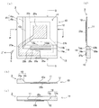
以下、本発明の実施の形態を図面に基づいて詳細に説明する。図1は、本発明の一実施形態に係る圧電振動素子1の構成を示す概略図である。図1(a)は圧電振動素子1の平面図であり、(b)はP−P断面を+X軸方向からみた断面図であり、(c)はP−P断面を−X軸方向からみた断面図であり、(d)はQ−Q断面を+Z’軸方向からみた断面図である。
圧電振動素子1は、矩形で薄肉の振動領域を含む振動部12、及び振動領域12と一体化され振動領域12よりも厚みが厚い支持部13を有する圧電基板10と、振動領域12の表面及び裏面に夫々配置された励振電極25a、25bと、各励振電極25a、25bから夫々支持部13に設けられたパッド電極29a、29bに向けて夫々延在して設けられたリード電極27a、27bと、を備えている。ここで、振動領域とは振動エネルギーが閉じ込められている領域、即ち振動エネルギーがほぼ零となる領域を言い、X軸方向の振動領域の寸法と、Z’軸方向の振動領域の寸法との比は周知のように、1.26:1である。また、振動部とは振動領域とその周縁部とを含んだ圧電基板全体をいう。
Hereinafter, embodiments of the present invention will be described in detail with reference to the drawings. FIG. 1 is a schematic view showing a configuration of a
The
圧電基板10は、矩形状であり、且つ薄肉で平板状の振動領域12と、振動領域12の四辺のうちの一辺12aに沿って配置された第1の支持部14と、振動領域12の一辺12aと隣接する他の一辺12bに沿って配置された第2の支持部15と、を備えている。つまり、圧電基板10は、振動領域12の隣接する二辺12a、12bに沿って一体化されたL字状の厚肉支持部(支持部)13(14、15)を備えている。
第1の支持部14は、薄肉平板状の振動領域12の一辺12aに連設し、振動領域12の一辺12aに連接する一方の端縁(内側端縁)から他方の端縁(外側端縁)に向かって離間するにつれて厚みが漸増する第1の傾斜部14bと、第1の傾斜部14bの前記他方の端縁(外側端縁)に連設する厚肉四角柱状の第1の支持部本体14aと、を備えている。同様に、第2の支持部15は、薄肉の平板状の振動領域12の一辺12bに連設し、振動領域12の一辺12bに連接する一方の端縁(内側端縁)から他方の端縁(外側端縁)に向かって離間するにつれて厚みが漸増する第2の傾斜部15bと、第2の傾斜部15bの前記他方の端縁(外側端縁)に連設する厚肉四角柱状の第2の支持部本体15aと、を備えている。
The
The
振動領域12の一方の主面(裏面)と、第1及び第2の支持部14、15の夫々の一方の主面(裏面)とは、同じ平面上、即ち図1に示す座標軸のX−Z’平面と平行な面上にあり、この一方の主面(図1(b)の裏面側)をフラット面(平坦面)といい、他方の主面である反対側の面(図1(b)の表面側)を凹陥面という。
第1及び第2の支持部14、15は、圧電基板の前記他方の主面側(表面側)にのみ突設されて設けられている。
第1の支持部14の一方の主面は、振動部12の一方の主面(表面)よりも突設して形成されている。そして、前記第1の支持部14の他方の主面と前記振動部の他方の主面とは連続的に連接されており、同一面となるよう構成されている。なお、振動領域にメサ上の突出したエネルギー閉じ込め領域がある場合についても、振動領域の周縁部の主面が前記前記第1の支持部14の他方の主面と連続的に連接されており、同一面となるように構成されていればよい。
第2の支持部15の一方の主面は、振動部12の一方の主面(表面)よりも突設して形成されている。そして、前記第2の支持部15の他方の主面と前記振動部の一方の主面とは連続的に連接されており、同一面となるよう構成されている。なお、振動領域にメサ上の突出したエネルギー閉じ込め領域がある場合についても、振動領域の周縁部の主面が前記前記第2の支持部15の他方の主面と連続的に連接されており、同一面となるように構成されていればよい。
第1の支持部14には、圧電振動素子1の実装にともなう少なくとも一つの応力緩和用のスリット20が、振動領域12と、被支持部であるパッド電極29a、29bとの間に、Z’方向に沿って貫通するように形成されている。図1に示した実施形態例では、スリット20は第2の傾斜部14bと第1の支持部本体14aとの境界部(連接部)に沿って第1の支持部本体14aの面内に形成されている。
なお、支持部本体(14a、15a)とは、Y’軸方向の厚みが一定の領域をいう。
One main surface (back surface) of the
The first and
One main surface of the
One main surface of the
The
The support body (14a, 15a) refers to a region having a constant thickness in the Y′-axis direction.
水晶等の圧電材料は三方晶系に属し、図2に示すように互いに直交する結晶軸X、Y、Zを有する。X軸、Y軸、Z軸は、夫々電気軸、機械軸、光学軸と呼称される。そして水晶基板は、XZ面をX軸の回りに所定の角度θだけ回転させた平面に沿って、水晶から切り出された平板が圧電振動素子用として用いられる。例えば、ATカット水晶基板10の場合は、θは略35°15′である。なお、Y軸及びZ軸もX軸の周りにθ回転させて、夫々Y’軸、及びZ’軸とする。従って、ATカット水晶基板10は、直交する結晶軸X、Y’、Z’を有する。ATカット水晶基板10は、厚み方向がY’軸であって、Y’軸に直交するXZ’面(X軸及びZ’軸を含む面)が主面であり、厚みすべり振動が主振動として励振される。
A piezoelectric material such as quartz belongs to the trigonal system and has crystal axes X, Y, and Z orthogonal to each other as shown in FIG. The X axis, the Y axis, and the Z axis are referred to as an electric axis, a mechanical axis, and an optical axis, respectively. In the quartz substrate, a flat plate cut out from the quartz along a plane obtained by rotating the XZ plane around the X axis by a predetermined angle θ is used for the piezoelectric vibration element. For example, in the case of the AT-
即ち、圧電基板10は、図2に示すようにX軸(電気軸)、Y軸(機械軸)、Z軸(光学軸)からなる直交座標系のX軸を中心として、Z軸をY軸の−Y方向へ傾けた軸をZ’軸とし、Y軸をZ軸の+Z方向へ傾けた軸をY’軸とし、X軸とZ’軸に平行な面で構成され、Y’軸に平行な方向を厚みとするATカット水晶基板である。
圧電基板10は、図1(a)に示すように、Y’軸に平行な方向(以下、「Y’軸方向」という)を厚み方向として、X軸に平行な方向(以下、「X軸方向」という)を長辺とし、Z’軸に平行な方向(以下、「Z’軸方向」という)を短辺とする矩形の形状を有する。
なお、圧電基板10は矩形状に限定されるものではなく、正方形、その他の四角形状であってもよい。また、本発明に係る圧電基板は、前記角度θが略35°15′のATカットに限定されるものではなく、厚みすべり振動を励振するBTカット等の圧電基板にも広く適用できるのは言うまでもない。
That is, as shown in FIG. 2, the
As shown in FIG. 1A, the
The
圧電基板10を駆動する励振電極25a、25bは、図1に示す実施形態例では四角形状であり、振動領域12のほぼ中央部の表裏両面(上面、及び下面両面)に対向して形成されている。裏面(フラット面)側の励振電極25bの面積の大きさは、表面側(凹陥面側)の励振電極25aの大きさに対し、十分に大きく設定する。これは、励振電極の質量効果によるエネルギー閉じ込め係数を、必要以上に大きくしないためである。つまり、裏面側(フラット面側)の励振電極25bを十分に大きくすることにより、プレートバック量Δ(=(fs−fe)/fs、ここでfsは圧電基板のカットオフ周波数、feは圧電基板全面に励振電極を付着した場合の周波数)は、表面側(上面側)の励振電極25aの質量効果のみに依存する。
In the embodiment shown in FIG. 1, the
励振電極25a、25bは、蒸着装置、あるいはスパッター装置等を用いて、例えば、下地にニッケル(Ni)を成膜し、その上に金(Au)を重ねて成膜する。金(Au)の厚さは、オーミックロスが大きくならない範囲で、主振動(S0)のみを閉じ込めモードとし、斜対称インハーモニック・モード(A0、A1・・)、及び対称インハーモニック・モード(S1、S3・・)を、閉じ込めモードとしないことが望ましい。しかし、例えば、490MHz帯という極めて高い高周波帯の圧電振動素子を構成しようとすると、電極膜厚のオーミックロスを避けるように成膜すると、低次のインハーモニック・モードが閉じ込めモードになることは避けられない。
表面側に形成した励振電極25aから延出したリード電極27aは、振動領域12上から第2の傾斜部15bと、第2の支持部本体15aとを経由して、第1の支持部本体14aの上面に形成されたパッド電極29aに導通接続されている。また、裏面側に形成された励振電極25bから延出したリード電極27bは、圧電基板10の裏面の端縁部を経由して、第1の支持部本体14aの裏面に形成されたパッド電極29bと導通接続されている。
The
The
図1(a)に示した実施形態例は、リード電極27a、27bの引出し構造の一例であり、リード電極27aは他の支持部を経由してもよい。ただ、リード電極27a、27bの長さは最短であることが望ましく、リード電極27a、27b同志が圧電基板10を挟んで交差しないように配慮することにより静電容量の増加を抑えることが望ましい。
また、図1の実施形態例では、圧電基板10の表裏面に対向して夫々パッド電極29a、29bを形成する例を示した。圧電振動素子1をパッケージに収容する際に、後述するように、圧電振動素子1を裏返し、パッド電極29aとパッケージの素子搭載パッドとを導電性接着剤で機械的に固定・電気的に接続し、パッド電極29bとパッケージの電極端子とをボンディングワイヤーを用いて電気的に接続する。このように圧電振動素子1を支持する部位が一点になると、導電性接着剤に起因して生じる応力を小さくすることが可能である。
The embodiment shown in FIG. 1A is an example of a lead-out structure of the
Further, in the embodiment example of FIG. 1, an example in which the
振動領域12と、圧電振動素子1の支持部であるパッド電極29a、29bとの間にスリット20を設ける理由は、導電性接着剤の硬化時に発生する応力の広がりを防止することにある。
即ち、圧電振動素子をパッケージに導電性接着剤により接着・固定する場合には、まず第1の支持部本体14aの被支持部(パッド電極)29aに導電性接着剤を塗布し、これをパッケージ等の素子搭載パッドに載置し、加重をかける。導電性接着剤を硬化させるために高温で所定の時間保持する。高温状態では第1の支持部本体14a、及びパッケージも共に膨張し、接着剤も一時的に軟化するので、第1の支持部本体14aには応力は生じない。導電性接着剤が硬化し、第1の支持部本体14a、及びパッケージが冷却してその温度が常温(25℃)に戻ると、導電性接着剤、パッケージ、及び第1の支持部本体14aの各線膨張係数の差により、硬化した道電性接着剤から生じる応力が生じる。この応力は、第1の支持部本体14aから第2の支持部15へ、第1の傾斜部14b、及び第2の傾斜部15bから振動領域12へと広がる。この応力の広がりを防止するために、応力緩和用のスリット20を設けている。
このように、スリット20を第1の支持本体14aの前記境界部(連接部)へ寄せて配置したので、第1の支持部本体14aの被支持部(パッド電極)29aの面積を広く確保することができ、塗布する導電性接着剤の径を大きくすることができる。これに対して、スリット20が第1の支持本体14aの被支持部(パッド電極)29a寄りに配置されると、被支持部(パッド電極)29aの面積が狭くなり、導電性接着剤の径を小さくしなければならない。その結果、導電性接着剤内に含まれる導電フィラーの絶対量も減り、導電性が悪化し、圧電振動素子1の共振周波数が安定しなくなり周波数変動(通称、F飛び)が発生しやすくなる虞がある。
従って、スリット20は第1の支持本体14aの前記境界部(連接部)へ寄せて配置することが好ましい。
The reason why the
That is, when the piezoelectric vibration element is bonded and fixed to the package with a conductive adhesive, first, the conductive adhesive is applied to the supported portion (pad electrode) 29a of the first supporting portion
Thus, since the
Therefore, it is preferable that the
圧電基板10に生じる応力(∝歪)分布を求めるために、有限要素法を用いてシミュレーションを行うのが一般的である。振動領域12における応力が少ない程、周波数温度特性、周波数再現性、周波数エージング特性等の優れた圧電振動素子が得られる。
導電性接着剤としては、シリコーン系、エポキシ系、ポリイミド系、ビスマレイミド系等が一般に用いられているが、脱ガスによる圧電振動素子1の周波数経年変化を考慮に入れて、ポリイミド系の導電性接着剤を用いた。ポリイミド系の導電性接着剤は硬いので、離れた二カ所を支持する(2点支持)よりも一カ所支持の方が、発生する応力の大きさを低減できる。このため、100〜500MHzの高周波数帯、例えば490MHzの電圧制御型圧電発振器(Voltage Controlled Crystal Oscillator:VCXO)用の圧電振動素子1には、一カ所支持(一点支持)構造を用いた。つまり、後述するように、パッド電極29aは導電性接着を用いてパッケージの素子搭載パッドに機械的に固定すると共に、電気的にも接続し、他方のパッド電極29bはパッケージの電極端子とボンディングワイヤーを用いて電気的に接続することにした。
In order to obtain the stress (strain) distribution generated in the
Silicone-based, epoxy-based, polyimide-based, bismaleimide-based, etc. are generally used as the conductive adhesive, but taking into account the frequency aging of the
また、図1に示した圧電基板10の外形は、X軸方向の長さがZ’軸方向の長さより長い、所謂Xロングとした。これは、圧電基板10が導電性接着剤等で接着・固定される際に応力が生じるが、周知のように、ATカット水晶基板のX軸方向の両端に圧力を加えたときの周波周変化と、Z’軸方向の両端に同じ圧力を加えたときの周波周変化と、を比べると、Z’軸方向の両端に圧力を加えたときの方が、周波数変化が小さい。つまり、支持点はZ’軸方向に沿って設ける方が応力による周波数変化は小さくなり、好ましい。
Further, the outer shape of the
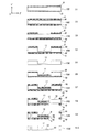
図3(a)は、圧電基板10上に形成されたリード電極27a、27b、及びパッド電極29a、29bの配置、構成を示す平面図であり、同図(b)は励振電極25a、25bの配置、構成を示す平面図である。リード電極27aは、表面の想定する励振電極25aの端縁から延在され、第2の支持部15の表面を経由し、第1の支持部14の中央部の表面に設けられたパッド電極29aに連設するように形成する。また、リード電極27bは、裏面の想定する励振電極25bの端縁から延在され、裏面(フラット面)の周縁に沿って、第1の支持部14の中央部の裏面に設けられたパッド電極29bに連設するように形成する。リード電極27a、27bは、夫々クロム(Cr)の薄膜から成る第1層と、この第1層上に積層された金(Au)の薄膜から成る第2層と、を備えている。リード電極27aの一部27aAのR−R断面を拡大した図を、左側の破線円27Aの中に示す。第2の支持本体15aの表面側(上面側)にクロムの薄膜27cを下地とし、この上に金の薄膜27gを積層成膜して、リード電極27aを構成する。リード電極27bについても同様である。
3A is a plan view showing the arrangement and configuration of the
また、第1の支持部14の中央部の表裏面に設けられたパッド電極29a、29bは、夫々クロム(Cr)の薄膜から成る第1層と、この第1層上に積層された金(Au)の薄膜から成る第2層と、を備えている。パッド電極29aの一部29AのT−T断面を拡大した図を、下部の破線円29Aの中に示す。第1の支持本体14aの表面側(上面側)にクロムの薄膜29cを下地とし、この上に金の薄膜29gを積層成膜してパッド電極29aを構成する。パッド電極29bについても同様である。
リード電極27a、27b、及びパッド電極29a、29bは、同一工程で形成されるため、膜厚の一例は、第1層のクロム(Cr)の薄膜が100Å(1Å=0.1nm(ナノメートル))、金(Au)の薄膜が2000Åと厚く形成されている。このため、リード電極27a、27b、及びパッド電極29a、29bのオーミックロスは生ぜず、ボンディング強度も十分である。
なお、クロム(Cr)薄膜と金(Au)薄膜との間に、他の金属膜を挟んだ構成でもよい。
The
Since the
Note that another metal film may be sandwiched between a chromium (Cr) thin film and a gold (Au) thin film.
図3(b)は、前工程で形成されたリード電極27a、27bと整合するように、圧電基板10上に形成した励振電極25a、25bの配置、構成を示す平面図である。凹陥部11のある表面側に励振電極25aを形成し、裏面側(フラット面側)に励振電極25aの面積より十分に大きく、且つ励振電極25aが面積内に納まる励振電極25bを形成する。
ここで、励振電極25a、25bの形成においては、前工程で先に形成したリード電極27a、27bと少なくとも一部が重なり合うように励振電極25a、25bを形成する。例えば、図3(b)に示すように、励振電極25aは、端部から延在されたリード電極の一部分27dを有している。当該リード電極の一部分27dが、リード電極27aの表面に重なり合うように構成されている。このように構成することにより、励振電極25aとリード電極27aとを電気的に確実に接続することができ、導通不良をきたすことを防止することができる。裏面側(フラット面側)に形成する励振電極25bについても同様な構成としている。
又は、前工程で先に形成するリード電極27bの一部分が、励振電極25bの領域に入り込む(重なり合う)ように形成してもよい。その際、共振周波数を決定するプレートバック量は、前記表面側である凹陥側の主面に形成される励振電極25aの質量効果のみに依存しているので、プレートバック量が設計値から変化しないように、リード電極27bの一部分が、励振電極25aと圧電基板10を挟んで重ならないように、励振電極25aの外形よりも外側に位置するように構成する。
励振電極25a、25bの構成の一例は、ニッケル(Ni)の薄膜から成る第1層と、この第1層上に積層された金(Au)の薄膜から成る第2層と、を備えている。励振電極25a、25bの一部、破線円のU−U断面図を右側の破線円内に示す。振動領域12の表裏面の一層目にニッケル(Ni)の薄膜25nが、二層目に金(Au)の薄膜25gが、積層して成膜されている。膜厚の一例は、第1層のニッケル(Ni)の薄膜が70Åであり、金(Au)の薄膜が600Åである。
なお、ニッケル(Ni)薄膜と、金(Au)薄膜との間に他の金属膜を挟んだ構成でもよい。
FIG. 3B is a plan view showing the arrangement and configuration of the
Here, in forming the
Or you may form so that a part of
An example of the configuration of the
Note that another metal film may be sandwiched between a nickel (Ni) thin film and a gold (Au) thin film.
圧電基板10の振動領域12の基本波周波数を490MHzという極めて周波数の高い高周波数帯とした場合、リード電極27a、27b、及びパッド電極29a、29bと、励振電極25a、25bとの夫々の電極材料、及び電極膜厚を異ならせる理由を以下に説明する。リード電極27a、27b、パッド電極29a、29b、及び励振電極25a、25bを、例えば第1層に70Åのニッケル(Ni)の薄膜、第2層に600Åの金(Au)の薄膜で構成するとする。主振動は十分に閉じ込めモードとなり、そのクリスタルインピーダンス(CI;等価抵抗)も小さくなるが、リード電極27a、27bの金(Au)の膜厚が薄いために、薄膜のオーミックロスが生じる虞がある。更に、パッド電極29a、29bが、70Åのニッケル(Ni)の薄膜と、600Åの金(Au)の薄膜とで形成されていると、ワイヤボンディングの強度不足を来たす虞がある。
When the fundamental frequency of the
また、リード電極27a、27b、パッド電極29a、29b、及び励振電極25a、25bを、例えば第1層に70Åのクロム(Cr)の薄膜、第2層に600Åの金(Au)の薄膜で構成すると、金(Au)の薄膜が薄いため、熱によりクロム(Cr)が金(Au)の薄膜内に拡散し、薄膜のオーミックロスが生じ、主振動のCIが大きくなるという虞が生じる。
The
そこで、本発明では、リード電極27a、27b、及びパッド電極29a、29bと、励振電極25a、25bとの形成工程を分離し、且つ夫々の電極薄膜の材料、及び膜厚を、夫々の薄膜の機能に最適になるように設定することにした。つまり、励振電極25a、25bは、主振動を閉じ込めモードとし、近接したインハーモニック・モードはできるだけ伝搬モード(非閉じ込めモード)となるように、例えば電極膜厚をニッケル(Ni)70Å、金600Åと薄く設定した。一方、リード電極27a、27b、及びパッド電極29a、29bは、細いリード電極の膜抵抗を低減し、且つボンディングの接着強度を高めるべく、クロム(Cr)の膜厚100Å、金(Au)の膜厚2000Åと厚めに設定した。
上記の膜厚は一例であり、この数値に限定するものではない。励振電極25a、25bに、エネルギー閉じ込め理論と、薄膜のオーミックロスとを考慮して、最適の膜厚のニッケル(Ni)及び金(Au)の積層膜を用いた。また、リード電極27a、27b、及びパッド電極29a、29bの膜厚は、薄膜のオーミックロスと、ボンディング強度とを考慮して、必要な厚さのクロム(Cr)と金(Au)の積層膜を用いた。
励振電極25a、25b、リード電極27a、27b、及びパッド電極29a、29bの製造方法については後述する。
Therefore, in the present invention, the formation process of the
The above film thickness is an example and is not limited to this value. In consideration of energy confinement theory and thin film ohmic cross, a multilayer film of nickel (Ni) and gold (Au) having an optimum film thickness was used for the
A method for manufacturing the
図1の実施形態例では、励振電極25a、25bの形状として四角形、つまり正方形、または矩形(X軸方向を長辺とする)とした例を示したが、これに限定する必要はない。図4に示す実施形態例は、表面側の励振電極25aが円形であり、裏面側の励振電極25bは、励振電極25aの面積より十分に大きな四角形である。なお、裏面側の励振電極25bが、面積の十分に大きな円形であってもよい。
図5に示す実施形態例は、表面側の励振電極25aが楕円形であり、裏面側の励振電極25bは、励振電極25aの面積より十分に大きな四角形である。水晶の場合、弾性定数の異方性によりX軸方向の変位分布と、Z’軸方向の変位分が異なり、変位分布をX−Z’平面に平行な面で切った切断面は、楕円形になる。そのため、楕円形状の励振電極25aを用いた場合が最も効率よく、圧電振動素子1を駆動できる。即ち、圧電振動素子1の容量比γ(=C0/C1、ここで、C0は静電容量、C1は直列共振容量)を最小にできる。また、励振電極25aは長円形であってもよい。
In the embodiment shown in FIG. 1, an example in which the
In the embodiment shown in FIG. 5, the
図6は、第2の実施形態に係る圧電振動素子2の構成を示す概略図である。図6(a)は圧電振動素子2の平面図であり、(b)はP−P断面を+X軸方向からみた断面図であり、(c)はP−P断面を−X軸方向からみた断面図であり、(d)はQ−Q断面を+Z’軸方向からみた断面図である。
圧電振動素子2が、図1に示す圧電振動素子1と異なる点は、応力緩和用のスリット20を設ける位置にある。本例では、スリット20は、薄肉の振動領域12の一辺12aの端縁より離間した第1の傾斜部14b内に形成されている。振動領域12の一辺12aに沿って、スリット20の一方の端縁が一辺12aに接するように、第1の傾斜部14b内にスリット20を形成するのではなく、第1の傾斜部14bの両端縁より離間してスリット20を設けている。つまり第1の傾斜部14bには、振動領域12の一辺12aの端縁と連接する極細の傾斜部14bbが残されている。換言すれば、一辺12aとスリット20との間に極細の傾斜部14bbが形成されている。
FIG. 6 is a schematic diagram illustrating a configuration of the
The piezoelectric vibrating
極細の傾斜部14bbを残した理由は次の通りである。即ち、振動領域12に配置された励振電極25a、25bに高周波電圧を印加して振動領域12を励振すると、主振動(S0)の他にインハーモニック・モード(A0、S1、A1、S2・)が励振される。望ましくは、主振動(S0)モードのみを閉じ込めモードとし、他のインハーモニック・モードは伝搬モード(非閉じ込めモード)とすることである。しかし、振動領域12が薄く成り、その基本波周波数が数百MHzとなると、電極膜のオーミックロスを避けるため、励振電極は所定の厚さ以上にする必要がある。このため、前記励振電極の厚みを前記所定の厚さ以上とした場合に、主振動に近接した低次のインハーモニック・モードが閉じ込めモードになる。本願発明者は、この低次のインハーモニック・モードの振幅の大きさ(CI)を抑制するには、インハーモニック・モードの定在波が成り立つ条件を妨げるようにすればよいことに思い至った。つまり、図6の振動領域12のZ’軸方向の両端縁の形状は非対称であり、またX軸方向の両端縁の形状も細片14bbを残して非対称である、低次のインハーモニック・モードの定在波の振幅が、抑えられることが判明した。
The reason for leaving the ultra-thin inclined portion 14bb is as follows. That is, when a high frequency voltage is applied to the
図7は、第3の実施形態に係る圧電振動素子3の構成を示す概略図である。図7(a)は圧電振動素子3の平面図であり、(b)はP−P断面を+X軸方向からみた断面図であり、(c)はP−P断面を−X軸方向からみた断面図であり、(d)はQ−Q断面を+Z’軸方向からみた断面図である。
圧電振動素子3が、図1に示す圧電振動素子1と異なる点は、第1の支持部本体14aの面内に第1のスリット20aを設けると共に、第1の傾斜部14bの面内に第2のスリット20bを形成して、2個の応力緩和用のスリットを設けた点である。第1の支持部本体14aの面内、及び第2の傾斜部14bの面内に夫々個別のスリットを形成する目的は、既に説明しているので、ここでは省略する。
FIG. 7 is a schematic diagram illustrating a configuration of the
The
図8(a)は、図7に示した圧電振動素子3の変形例の構成を示す平面図である。第1のスリット20aは、第1の支持部本体14aの面内に設けられており、第2のスリット20bは、第1の傾斜部14bの面内に設けられている。しかし、第1のスリット20a、及び第2のスリット20bは、図7(a)に示す平面図のように、X軸方向に並置するのではなく、Z’軸方向に互いに離れるように段差状にずらして配置されている点が圧電振動素子3と異なる。2個のスリット20a、20bを設けることにより、導電性接着剤に起因して生じる応力を、振動領域12まで広げないように抑圧する効果を高めることができる。
図8(b)は図1、6に示す第1、及び第2実施形態の圧電振動素子1、2の変形例であり、スリット20は、第1の支持部本体14aと第1の傾斜部14bとの両者に跨って形成されている。このようにスリット20を形成することにより、図1、6の構造の効果を同時に満たす効果を期待でき、導電性接着剤に起因して生じる応力を、振動領域12まで広げないように抑圧する効果を高めることができる。
FIG. 8A is a plan view showing a configuration of a modification of the
FIG. 8B is a modification of the
図9は、図1に示した実施形態例の圧電振動素子1の変形例の構成を示す平面図である。リード電極27aは、表面の励振電極25aの端縁から延在され、第2の支持部15の表面を経由し、第1の支持部14の中央部の表面に設けられたパッド電極29aに連設するように形成されている。また、リード電極27bは、裏面の励振電極25bの端縁から延在され、裏面の端部を経由し、第1の支持部14の中央部の裏面に設けられたパッド電極29bに連設するように形成されている。図1に示した実施形態例の圧電振動素子1と異なる点は、パッド電極29a、29bが配置される位置である。パッド電極29a、29bは第1の支持部本体14aの表面に、互いに離れて設けられている。パッド電極29bは、裏面に形成されたリード電極27bと導通するように、圧電基板10の端縁に跨って導体薄膜が形成されている。表面側のパッド電極29a、29bに導電性接着剤を塗布し、これを反転してパッケージの素子搭載パッドに載置する際に、容易に導通が図られるように、パッド電極29a、29bが構成されている。
即ち、図9の実施形態例では圧電振動素子1の一方の面の第1の支持部14の2カ所(2点)に導電性接着剤を塗布して、導通と支持・固定を図るようにした構造である。低背化に適した構造であるが、導電性接着剤に起因する応力が少し大きくなる虞がある。そこで、第3の実施形態である図7や図8に示すようなスリットを2つ設けた圧電振動素子を採用することで、前記応力の振動領域への影響を抑圧できることが期待できる。または、導電性接着剤の硬度が比較的硬い場合には、導電性接着剤を塗する「2カ所(2点)」の中心間距離を狭めることにより、前記2点間で生じる実装に係る歪み(応力)を低減させる手法もある。また一方、導電性接着剤の硬度が比較的柔らかい、シリコーン系接着剤を用いることにより、導電性接着剤に緩衝性を持たせ、前記2点間で生じる実装に係る歪み(応力)を低減させる手法もある。
FIG. 9 is a plan view showing a configuration of a modification of the
That is, in the embodiment of FIG. 9, a conductive adhesive is applied to two places (two points) of the
図10は、圧電基板10の凹陥部11、外形及びスリットの形成に係る製造工程図である。ここでは、圧電ウエハーとして水晶ウエハーを例にし、図は断面のみを示す。工程S1では、両面がポリッシュ加工された所定の厚さ、例えば80μmの水晶ウエハー10Wを、十分に洗浄し、乾燥した後、表裏面にスパッタリング等により、クロム(Cr)を下地にし、その上に金(Au)を積層した金属膜(耐蝕膜)Mを夫々成膜する。
工程S2では、表裏面の金属膜Mの上に夫々フォトレジスト膜(レジスト膜と称す)Rを両面に塗布する。工程S3では、露光装置とマスクパターンを用いて、表裏面の凹陥部に相当する部位のレジスト膜Rを露光する。感光したレジスト膜Rを現像して、感光したレジスト膜を剥離すると、表裏面の凹陥部に相当する位置の金属膜Mが夫々露出する。夫々のレジスト膜Rから露出した各金層膜Mを王水等の溶液を用いて溶かして除去すると、表裏面の凹陥部に相当する位置の水晶面が露出する。
FIG. 10 is a manufacturing process diagram relating to the formation of the recessed
In step S2, a photoresist film (referred to as a resist film) R is applied to both surfaces of the metal film M on the front and back surfaces. In step S3, the resist film R in a portion corresponding to the recessed portions on the front and back surfaces is exposed using an exposure apparatus and a mask pattern. When the exposed resist film R is developed and the exposed resist film is peeled off, the metal films M at positions corresponding to the recessed portions on the front and back surfaces are exposed. When the gold layer films M exposed from the respective resist films R are dissolved and removed using a solution such as aqua regia, the crystal planes at positions corresponding to the recessed portions on the front and back surfaces are exposed.
工程S4では、露出した水晶面をフッ化水素酸(フッ酸)とフッ化アンモニウムとの混合液を用いて、所望の厚さになるまで表面からエッチングする。工程S5では、所定の溶液を用いて両面のレジスト膜Rを剥離し、更に露出した両面の金属膜Mを、王水等を用いて除去する。この段階で水晶ウエハー10Wは、片面に形成された凹陥部11が、格子状に規則的に並んだ状態となる。工程S6では、工程S5で得られた水晶ウエハー10Wの両面に金属膜M(Cr+Au)を成膜する。工程S7では、工程S6で形成された金属膜M(Cr+Au)の両面に夫々レジスト膜Rを塗布する。
工程S8では、露光装置と所定のマスクパターンを用いて、圧電基板10の外形とスリット(図示されず)とに相当する部位の各レジスト膜Rを表裏両面から感光し、現像して、各レジスト膜Rを剥離する。更に、露出した金属膜Mを王水等の溶液で溶かして除去する。
In step S4, the exposed quartz surface is etched from the surface using a mixed solution of hydrofluoric acid (hydrofluoric acid) and ammonium fluoride until a desired thickness is obtained. In step S5, the resist films R on both sides are peeled off using a predetermined solution, and the exposed metal films M on both sides are removed using aqua regia or the like. At this stage, the
In step S8, each resist film R in a portion corresponding to the outer shape of the
工程S9では露出した水晶面をフッ化水素酸(フッ酸)とフッ化アンモニウムとの混合液を用いてエッチングし、圧電基板10の外形とスリットを形成する。工程S10では、残ったレジスト膜Rを剥離し、露出した余分の金属膜Mを溶かして除去する。この段階では水晶ウエハー10Wは、圧電基板10が支持細片で連接し、格子状に規則的に並んだ状態となる。
なお、X軸に直交する断面の外形を示したが、Z’軸に直交する断面の外形も両面エッチングにより加工されて、図1に示すような形状となる。
工程S10が終了した後、水晶ウエハー10Wに格子状に規則的に並んだ各圧電基板10の振動領域12の厚さを、例えば光学的手法を用いて計測する。計測した各振動領域12の厚さが所定の厚さより厚い場合には、夫々厚さの微調整を行って所定の厚さの範囲に入るようにする。
In step S9, the exposed quartz surface is etched using a mixed liquid of hydrofluoric acid (hydrofluoric acid) and ammonium fluoride to form the outer shape of the
In addition, although the external shape of the cross section orthogonal to the X axis is shown, the external shape of the cross section orthogonal to the Z ′ axis is also processed by double-sided etching so that the shape shown in FIG. 1 is obtained.
After step S10 is completed, the thickness of the
次に、水晶ウエハー10Wに形成された各圧電基板10の振動領域12の厚さが、所定の厚さの範囲内に調整された後、各圧電基板10に励振電極25a、25b、及びリード電極27a、27bを形成する手順を、図11に示す製造工程図を用いて説明する。工程S11では、水晶ウエハー10Wの表裏全面にスパッタリング等でクロム(Cr)薄膜を成膜し、その上に金(Au)薄膜を積層して、金属膜Mを成膜する。次に工程S12では、金属膜Mの上に夫々レジストを塗布し、レジスト膜Rを成膜する。工程13では、リード電極、及びパッド電極用のマスクパターンMkを用いて、リード電極、及びパッド電極に相当する部位のレジスト膜Rを露光する。次の工程S14では、レジスト膜Rを現像し、不要のレジスト膜Rを剥離する。この剥離により露出した金属膜Mを王水等の溶液で溶かして除去する。リード電極、及びパッド電極上のレジスト膜はそのまま残しておく。
Next, after the thickness of the
次の工程S15では、水晶ウエハー10Wの表裏全面にスパッタリング等でニッケル(Ni)薄膜を成膜し、その上に金(Au)薄膜を積層して、金属膜Mを成膜する。更に、金属膜Mの上にレジスト膜Rを塗布する。工程S15の図では、煩雑さを避けるため、リード電極及びパッド電極用の金属膜とレジスト膜(M+R)を、記号Cを用いて表わしている。そして、励振電極用のマスクパターンMkを用いて、励振電極に相当する部位のレジスト膜Rを露光する。工程S16では、感光したレジスト膜Rを現像して不要のレジスト膜Rを、溶液を用いて剥離する。次の工程S17では、レジスト膜Rが剥離して露出した金属膜Mを王水等の溶液で溶かして除去する。工程S18では、符号C(リード電極及びパッド電極用の金属膜とレジスト膜)を(M+R)に戻して表わし、金属膜M上に残った不要のレジスト膜Rを剥離すると、各圧電基板10上には(Ni+Au)の励振電極25a、25bと、(Cr+Au)のリード電極27a、27b、及びパッド電極29a、29bが形成されている(工程S19)。水晶ウエハー10Wに連接するハーフエッチングされた支持細片を折り取りすることにより、分割された圧電振動素子が得られる。
In the next step S15, a nickel (Ni) thin film is formed on the entire front and back surfaces of the
ところで、水晶をウェットエッチングすると、Z軸に沿ってエッチングが進行していくが、各結晶軸の方向に応じてエッチングの速度が変わってくるという水晶特有のエッチング異方性を有している。従って、当該エッチングの異方性により現出するエッチング面は、各結晶軸の方向に応じて違いが現れることは、これまでエッチング異方性を研究テーマにした数多くの学術論文や先行特許文献において論じられてきた。しかしながら、このような背景があるにもかかわらず、水晶のエッチング異方性について明確に系統立てられた資料がなく、ナノ加工技術的側面が非常に強いためにエッチングの諸条件(エッチング溶液の種類や、エッチングレート、エッチング温度、等)の違いによるものなのか、文献によっては、現出する結晶面に相異があるものも多々見受けられるのが現状である。
そこで、本願発明者は、本発明に係る圧電基板をフォトリソグラフィー技法とウェットエッチング技法を用いて製造するに当たり、エッチングシミュレーションと試作実験、並びにナノレベルでの表面分析と観察を繰り返し、本発明に係る圧電振動子は以下の態様となることが判明したので、以下詳細に説明をする。
By the way, when the crystal is wet-etched, the etching proceeds along the Z-axis, but has an etching anisotropy peculiar to the crystal in which the etching rate varies depending on the direction of each crystal axis. Therefore, the etching surface that appears due to the anisotropy of the etching appears to differ depending on the direction of each crystal axis. Has been discussed. However, despite this background, there is no clearly organized data on the etching anisotropy of quartz, and the nanofabrication technical aspects are so strong that the etching conditions (types of etching solutions) Depending on the literature, there are many cases where there are differences in the crystal planes appearing, depending on the difference in the etching rate and etching temperature.
Therefore, the inventor of the present invention repeats etching simulation and trial production, and surface analysis and observation at the nano level in manufacturing the piezoelectric substrate according to the present invention using the photolithography technique and the wet etching technique, and the present invention relates to the present invention. The piezoelectric vibrator has been found to be in the following mode, and will be described in detail below.
図12、図13は、フォトリソグラフィー技術とエッチング手法により形成される、ATカット水晶ウエハー10W上の凹陥部11の断面形状を説明する図である。
図12(a)は、図10の工程S5における水晶ウエハー10Wの平面図である。この段階では、水晶ウエハー10Wの一方の面に凹陥部11が格子状で且つ規則的に形成されている。図12(b)は、X軸方向の断面図であり、凹陥部11の各壁面は垂直の壁面ではなく傾斜面を呈している。つまり、−X軸方向の壁面は傾斜面X1を形成し、+X軸方向の壁面は傾斜面X2を形成している。X軸に直交する溝を形成すると、溝の断面の壁面X3は楔型を呈する。図10(c)〜(e)は凹陥部11の壁面X1、X2、及び溝部の壁面X3の拡大図である。−X軸方向の壁面は、図10(c)に示すように、水晶ウエハー10Wの平面に対し略62度の傾斜でエッチングされる。+X軸方向の壁面は、図10(d)に示すように、水晶ウエハー10Wの平面に対し直交(90度)して少しエッチングが進むが、その後は緩やかな傾斜でエッチングが進行する。形成された凹陥部11の底面は、水晶ウエハーの元の平面と平行にエッチングされる。つまり、振動領域12は表裏面が平行の平板状となる。
図12(e)は、水晶ウエハー10Wに形成した折り取り用の溝部の断面図である。X軸に直交して形成された溝部の断面は楔型を呈している。これは溝部の壁面X3が、−X軸方向の壁面X1と、+X軸方向の壁面X2とで形成されるために、楔型となるのである。
凹陥部11が形成された面に電極を設ける場合は、+X軸方向に形成される壁面X2の垂直の壁面に注意する必要がある。電極膜の断裂が起り易いので避ける方が望ましい。
FIGS. 12 and 13 are diagrams for explaining the cross-sectional shape of the recessed
FIG. 12A is a plan view of the
FIG. 12E is a cross-sectional view of the groove portion for breaking formed in the
When providing an electrode on the surface on which the recessed
図13は圧電基板10に形成された凹陥部11の、特にZ’軸方向の断面図の壁面を説明する図である。図13(a)は、水晶ウエハー10Wの平面図である。図13(b)は、水晶ウエハー10WのZ’軸方向の断面図であり、−Z’軸方向の壁面は傾斜面Z1を形成し、+Z’軸方向の壁面は傾斜面Z2を形成する。Z’軸に直交する溝部を形成すると、溝部の断面の壁面Z3は楔型を呈する。
図11(c)〜(e)は凹陥部11の壁面Z1、Z2、及ぶ溝部の壁面Z3の拡大図である。−Z’軸方向の壁面は、図13(c)に示すように、水晶ウエハー10Wの平面に対し比較的緩やかな傾斜でエッチングされる。+Z’軸方向の壁面Z2は、図11(d)に示すように、水晶ウエハー10Wの平面に対し急な傾斜面Z2aでエッチングされるが、その後は緩やかな傾斜面Z2bでエッチングが進行し、その後はより緩やかな傾斜面Z2cとなる。図13(e)はZ’軸方向に直交して形成した溝部の断面図で、楔型断面Z3となる。この溝部は、水晶ウエハー10Wに折り取り用の溝部である。この溝部の壁面Z3が、−Z’軸方向の壁面Z1と、+Z’軸方向の壁面Z2の中、壁面Z2aと壁面Z2bとで形成されるために、ほぼ楔型の断面を呈するのである。X軸方向、Z’軸方向に折り取り用溝部を形成すると、その断面形状は楔型となり、折り取りが容易である。
FIG. 13 is a view for explaining the wall surface of the recessed
FIGS. 11C to 11E are enlarged views of the wall surfaces Z1 and Z2 of the recessed
本発明の特徴の1つは、図13(d)に示すように、振動領域11うちZcで示す一点鎖線の図中右側の、元の平面と平行でない緩やかな傾斜面Z2c、及びこれに連設する厚肉部17と、図12(d)に示す傾斜面X2、及びこれに連設する厚肉部16と、をエッチングにより取り去ることにより、圧電基板の小型化を図ったことである。つまり、振動領域12は、2つの隣接する辺をL字状の支持部13によって保持された圧電基板10である。
更に、前記緩やかな傾斜面Z2、及び厚肉部17と、傾斜面X2、及び厚肉部16と、を共に削除することを前提として製造方法を確立した。このため、振動領域となる平坦な超薄部の面積を、先行技術として掲げた、従来の如きX軸に沿って振動領域の両端に存在する厚肉部を備えた構造に比べて大きく確保することを実現した。その結果、振動領域に励振される厚み滑り振動モードにおいて、弾性定数の異方性により振動変位分布がX軸方向に長径を有する楕円状となることを十分に考慮して、設計することが可能となるため、長軸対短軸の比を、1.26:1が望ましいが、製造寸法のバラツキ等を考慮して、1.14〜1.39:1の範囲程度となるように十分設計可能となった。
One of the features of the present invention is that, as shown in FIG. 13 (d), a gentle inclined surface Z2c that is not parallel to the original plane on the right side of the dotted line indicated by Zc in the
Furthermore, a manufacturing method was established on the premise that both the gently inclined surface Z2 and the
図14は、図1に示した圧電振動素子1のより詳細な図であり、同図(a)は斜視図であり、同図(b)は図1(a)におけるQ−Q断面の切り口である。図14(a)、(b)に示すように、圧電振動素子1の外形は、X軸に交わる端面に傾斜面が現出する。つまり、−X軸側の端面には図14(a)の傾斜面1が現出し、+X軸側の端面には図14(b)の傾斜面2が現出している。傾斜面1と傾斜面2のXY’平面に平行な断面形状が、異なっている。
また、傾斜面1、2共に、圧電基板の主表面と交わる付近には、図12(b)、(d)に示すような+X軸方向に形成される壁面X2の垂直の壁面は現出していない。この理由は、凹陥部11を形成するのに必要なエッチング時間に比べて、傾斜面1と傾斜面2の形成時間は、圧電基板(水晶基板)を表裏からエッチングを開始し、表裏が貫通するまでエッチングするので、エッチング時間が十分に長いためにオーバーエッチングの作用により、垂直の壁面が現出しないのである。
傾斜面1を構成する傾斜面a1、a2は、X軸に対してほぼ対称関係にあり、傾斜面2を構成する傾斜面b1、b2、b3、b4では、b1とb4、b2とb3とが、各々X軸に対してほぼ対称関係にあることが判明した。更に、傾斜面a1、a2のX軸に対する傾斜角度αと、傾斜面b1、b4のX軸に対する傾斜角度βとは、β<αの関係にある。
14 is a more detailed view of the
In addition, in the vicinity where both the
The inclined surfaces a1 and a2 constituting the
図1、図6、図7の実施形態例に示すように、基本波を用いた高周波圧電振動素子が小型化され、量産化されると共に、支持部と振動領域の間にスリットを設けることにより、接着・固定に起因する応力の広がりを抑圧できるので、周波数温度特性、CI温度特性、及び周波数エージング特性に優れた圧電振動素子が得られるという効果がある。また、図3の実施形態例に示すように、励振電極25a、25と、リード電極27a、27b及びパッド電極29a、29bとは、夫々異種構成の金属材料が用いられ、且つ適切な膜厚で構成されているため、主振動のCI値が小さく、主振動のCI値に対する近接したスプリアスのCI値の比、即ちCI値比の大きな圧電振動素子が得られるという効果がある。
また、図1、図3の実施形態例に示すように、励振電極25a、25bはニッケルと金の積層膜で形成され、リード電極27a、27b、及びパッド電極29a、29bはクロムと金の積層膜で形成されているため、主振動のCI値が小さく、主振動のCI値に対する近接したスプリアスのCI値の比、即ちCI値比の大きな、ボンディングに十分耐えられる圧電振動素子が得られるという効果がある。
As shown in FIG. 1, FIG. 6, and FIG. 7, the high-frequency piezoelectric vibration element using the fundamental wave is miniaturized and mass-produced, and a slit is provided between the support portion and the vibration region. Since the spread of stress due to adhesion / fixation can be suppressed, there is an effect that a piezoelectric vibration element having excellent frequency temperature characteristics, CI temperature characteristics, and frequency aging characteristics can be obtained. Further, as shown in the embodiment of FIG. 3, the
1 and 3, the
圧電基板10が、図2の切断角度図に示されるように形成されるため、要求仕様の圧電振動素子を、より適したカットアングルで構成することが可能であり、且つ仕様にそった周波数温度特性を有し、CI値が小さく、CI値比の大きな高周波圧電振動素子が得られるという効果がある。
また、圧電基板10に水晶ATカット水晶基板を用いることにより、フォトリソグラフィー技術及びエッチング技法に関する実績・経験が活用できるので、圧電基板の量産が可能であるのみならず、高精度の圧電基板が得られ、CI値が小さく、CI値比の大きな圧電振動素子の量産が可能になるという効果がある。
Since the
In addition, by using a quartz AT-cut quartz substrate as the
図15は、本発明に係る実施形態の圧電振動子5の構成を示す図であり、同図(a)は縦断面図であり、同図(b)は蓋部材を省略した平面図である。圧電振動子5は、例えば圧電振動素子1と、圧電振動素子1を収容するパッケージとを備えている。パッケージは、矩形の箱状に形成されているパッケージ本体40と、金属、セラミック、ガラス等から成る蓋部材49とから成る。
パッケージ本体40は、図15に示すように、第1の基板41と、第2の基板42と、第3の基板43とを積層して形成されており、絶縁材料として、酸化アルミニウム質のセラミック・グリーンシートを成形し、箱状とした後で、焼結して形成される。実装端子45は、第1の基板41の外部底面に複数形成されている。第3の基板43は中央部が除去された環状体であり、第3の基板43の上部周縁に例えばコバール等の金属シールリング44が形成されている。
第3の基板43と第2の基板42とにより、圧電振動素子1を収容する凹部(キャビティ)が形成される。第2の基板42の上面の所定の位置には、導体46により実装端子45と電気的に導通する複数の素子搭載パッド47が設けられている。素子搭載パッド47の位置は、圧電振動素子1を載置した際に第1の支持部本体14aに形成したパッド電極29aに対応するように配置されている。
FIGS. 15A and 15B are diagrams showing a configuration of the
As shown in FIG. 15, the
The
圧電振動子5を固定する際にはまず、圧電振動素子1のパッド電極29aに導電性接着剤30を塗布し、これを反転(裏返し)してパッケージ本体40の素子搭載パッド47に載置して荷重をかける。導電性接着剤30の特性として、接着剤30に起因する応力(∝歪)の大きさは、シリコーン系接着剤、エポキシ系接着剤、ポリイミド系接着剤の順で大きくなる。また、脱ガスは、ポリイミド系接着剤、エポキシ系接着剤、シリコーン系接着剤の順で大きくなる。導電性接着剤30としては経年変化を考慮して脱ガスの少ないポリイミド系接着剤を用いることにした。
When fixing the
パッケージ本体40に搭載された圧電振動子1の導電性接着剤30を硬化させるために、所定の温度の高温炉に所定の時間入れる。導電性接着剤30を硬化させた後、反転して表面側になったパッド電極29bと、パッケージ本体40の電極端子48とをボンディングワイヤーBWで導通接続する。図15(b)に示すように、圧電振動素子1をパッケージ本体40に支持・固定する部分は、一カ所(1点)、即ちパッド電極29aと、素子搭載パッド47との固定部分だけであるため、支持固定により生じる応力の大きさを小さくすることが可能となる。
アニール処理を施した後、励振電極25a、25bに質量を付加するか、又は質量を減じて周波数調整を行う。パッケージ本体40の上面に形成したシールリング44上に、蓋部材49を載置し、真空中、又は窒素N2ガスの雰囲気中で蓋部材49をシーム溶接して密封し、圧電振動子5が完成する。又は、パッケージ本体40の上面に塗布した低融点ガラスに蓋部材49を載置し、溶融して密着する方法もある。この場合もパッケージのキャビティ内は真空にするか、又は窒素N2ガス等の不活性ガスで充填して、圧電振動子5が完成する。
In order to cure the
After the annealing treatment, the frequency is adjusted by adding mass to the
図1、図6、図7に示す夫々の圧電振動素子1、2、3は、圧電基板10の上下面に対向して夫々パッド電極29a、29bが形成されている。図15に示すように、圧電振動素子1をパッケージに収容する際に、圧電振動素子1を裏返し、パッド電極29aとパッケージの素子搭載パッド47とを導電性接着剤で固定・接続する。表面側になったパッド電極29bと、パッケージの電極端子48とをボンディングワイヤーBWで接続する。このように圧電振動素子1を支持する部位が一点になると、導電性接着剤に起因して生じる応力が小さくなる。また、パッケージに収容するに当たり、圧電振動素子1を裏返して、より大きな励振電極25bを上面にすると、圧電振動素子1の周波数微調が容易となる。
Each of the
また、パッド電極29a、29bの間隔を離して形成した圧電振動素子を用いて圧電振動子5を構成してもよい。この場合も図15で説明した圧電振動子5と同様に圧電振動子を構成することができる。
また図9に示すように、パッド電極29a、29bを同一面上に間隔を離して形成した圧電振動素子1を用いて圧電振動子5を構成してもよい。この場合、圧電振動素子は、パッド電極29a、29bに夫々導電性接着剤を塗布して、反転してパッケージ本体40に形成された素子搭載パッドに載置し、加重をかけて、支持・固定を図るようにした構造である。低背化に適した構造であるが、被支持部が2点となるので、導電性接着剤に起因する応力が少し大きくなる虞がある。
以上の圧電振動子5の実施の形態例では、パッケージ本体40に積層板を用いた例を説明したが、パッケージ本体40に単層セラミック板を用い、蓋体に絞り加工を施したキャップを用いて圧電振動子を構成してもよい。
Alternatively, the
Further, as shown in FIG. 9, the
In the above-described embodiment of the
図1、図6、図7の実施形態に示す圧電振動素子1、2、3を用いて、図15に示す圧電振動子を構成しているので、高周波圧電振動子が小型化されると共に、圧電振動素子1、2、3を支持する部位が一点であり、且つ支持部と振動領域の間にスリットを設けることにより、導電性接着剤に起因して生じる応力を小さくすることができるため、周波数再現性、周波数温度特性、CI温度特性、及び周波数エージング特性に優れた圧電振動子が得られるという効果がる。
また、図1、図3の実施形態例に示すように、励振電極25a、25bの電極材料と、リード電極27a、27b、及びパッド電極29a、29bの電極材料と、を異ならせ、又それらの膜厚も夫々の機能に最適なように構成した圧電振動素子1、2、3を用いているため、主振動のCI値が小さく、主振動のCI値に対する近接したスプリアスのCI値の比、即ちCI値比の大きな圧電振動子1、2、3が得られるという効果がある。
Since the piezoelectric vibrator shown in FIG. 15 is configured using the
1 and FIG. 3, the electrode materials of the
図16は、本発明に係る圧電デバイス6の実施形態を示す縦断面図である。電子デバイス6は、本発明の圧電振動素子1(圧電振動素子2、3でもよい)と、電子部品の1つであり、温度センサーとしての感温素子であるサーミスタThと、圧電振動素子1、及びサーミスタThを収容するパッケージと、を概略備えている。パッケージは、パッケージ本体40aと、蓋部材49とを備えている。パッケージ本体40aは、上面側に圧電振動素子1を収容するキャビティ31が形成され、外部下面側にサーミスタThを収容する凹部32が形成されている。キャビティ31の内底面の端部に素子搭載用パッド47が設けられ、素子搭載用パッド47は内部導体46で実装端子45と導通接続されている。圧電振動素子1のパッド電極29aに導電性接着剤30を塗布し、これを反転し、素子搭載用パッド47に載置する。反転して表面側になったパッド電極29bと電極端子48とをボンディングワイヤーBWで接続する。パッケージ本体40aの上部には、コバール等からなるシールリング44が焼成されており、このシールリング44に蓋部材49を載置し、抵抗溶接機等を用いて溶接し、キャビティ31を気密封止する。キャビティ31内は真空にしてもよいし、不活性ガスを封入してもよい。裏面の凹部32に半田ボール等を用いてサーミスタThの端子を接続して、電子デバイス6を完成する。
FIG. 16 is a longitudinal sectional view showing an embodiment of the
以上の実施形態例では、パッケージ本体40aの外部下面側に凹部32を形成し、電子部品を搭載した例を説明したが、パッケージ本体40aの内部底面に凹部32を形成し、電子部品を搭載してもよい。
また、圧電振動素子2とサーミスタThとをパッケージ40aに収容した例を説明したが、パッケージ40aに収容する電子部品としては、サーミスタ、コンデンサ、リアクタンス素子、半導体素子のうち少なくとも一つを収容して電子デバイスを構成することが望ましい。
In the above embodiment example, the
Moreover, although the example which accommodated the
図16に示す実施形態例のように、圧電振動素子1とサーミスタThとをパッケージ40aに収容した電子デバイス6を構成すると、感温素子のサーミスタThが圧電振動素子1の極めて近くに配置されているので、圧電振動素子1の温度変化を素早く感知することができるという効果がある。また、本発明の圧電振動素子と上記の電子部品とで電子デバイスを構成することにより、高周波、且つ小型の電子デバイスが構成できるので、多方面の用途に利用できるという効果がある。
また、電子部品に可変容量素子、サーミスタ、インダクタ、コンデンサーのうちの何れかを用いて電子デバイス(圧電デバイス)を構成すると、要求仕様により適した電子デバイスが、小型で且つ低コストで実現できるという効果がある。
When the
In addition, when an electronic device (piezoelectric device) is configured using any one of a variable capacitance element, thermistor, inductor, and capacitor as an electronic component, an electronic device suitable for the required specifications can be realized in a small size and at low cost. effective.
図17は、本発明の実施形態例に係る電子デバイスの一種である圧電発振器7の構成を示す図であって、同図(a)は縦断面図であり、同図(b)は蓋部材を省略した平面図ある。圧電発振器7は、パッケージ本体40b、及び蓋部材49と、圧電振動素子1と、圧電振動素子1を励振する発振回路を搭載したIC部品51と、電圧により容量が変化する可変容量素子、温度により抵抗が変化するサーミスタ、インダクタ等の電子部品52の少なくとも1つと、を備えている。
圧電振動素子1のパッド電極29aに導電性接着剤(ポリイミド系)30を塗布し、これを反転してパッケージ本体40bの素子搭載パッド47に載置し、パッド電極29aと素子搭載パッド47との導通を図る。反転して上面側になったパッド電極29bと、パッケージ本体40bの他の電極端子48とをボンディングワイヤーにて接続し、IC部品51の1つの電極端子55との導通を図る。IC部品51をパッケージ本体40bの所定の位置に固定し、IC部品51の端子と、パッケージ本体40bの電極端子55とをボンディングワイヤーBWにて接続する。また、電子部品52は、パッケージ本体40bの所定の位置に載置し、金属バンプ等を用いて接続する。パッケージ本体40bを真空、あるいは窒素等の不活性気体で満たし、パッケージ本体40bを蓋部材49で密封して電子デバイス(圧電発振器)7を完成する。
パッド電極29bとパッケージの電極端子48とをボンディングワイヤーBWで接続する工法は、圧電振動素子1を支持する部位が一点になり、導電性接着剤に起因して生じる応力を小さくする。また、パッケージに収容するに当たり、圧電振動素子1を反転して、より大きな励振電極25bを上面にしたので、電子デバイス(圧電発振器)7の周波数微調が容易となる。
FIG. 17 is a view showing a configuration of a
A conductive adhesive (polyimide) 30 is applied to the
In the method of connecting the
図17の実施形態に示した電子デバイス(圧電発振器)7は、同一圧電基板上に圧電振動素子1、IC部品51及び電子部品を配置したが、図18に示した実施形態の電子デバイス(圧電発振器)7は、H型のパッケージ本体60を用い、上部に形成したキャビティ31に圧電振動素子1を収容し、キャビティ内部を真空、又は窒素N2ガスで満たし、蓋部材61で密封する。下部には圧電振動素子1を励振する発振回路、増幅回路等を搭載したIC部品51と、可変容量素子、及び必要に応じてインダクタ、サーミスタ、コンデンサー等の電子部品52と、を金属バンプ(Auバンプ)68を介して、パッケージ本体60の端子67に導通・接続する。
本発明の電子デバイス(圧電発振器)7は、圧電振動素子1と、IC部品51及び電子部品52とを分離し、圧電振動素子1を単独で気密封止しているために、圧電発振器7の周波数エージング特性が優れている。
In the electronic device (piezoelectric oscillator) 7 shown in the embodiment of FIG. 17, the
The electronic device (piezoelectric oscillator) 7 according to the present invention separates the
図17、図18に示すように、圧電デバイス(例えば電圧制御型圧電発振器)を構成することにより、周波数再現性、周波数温度特性、エージング特性が優れ、小型で且つ高周波(例えば490MHz帯)の電圧制御型圧電発振器が得られるという効果がある。また、圧電デバイスは基本波の圧電振動素子1を用いているので、容量比が小さく、周波数可変幅が広がる。更に、S/N比の良好な電圧制御型圧電発振器が得られるという効果がある。
また、圧電デバイスとして圧電発振器、温度補償型圧電発振器等を構成することが可能であり、周波数再現性、エージング特性、周波数温度特性に優れた圧電発振器を構成することができるという効果がある。
As shown in FIGS. 17 and 18, by configuring a piezoelectric device (for example, a voltage-controlled piezoelectric oscillator), the frequency reproducibility, frequency temperature characteristics, and aging characteristics are excellent, and the voltage is small and has a high frequency (for example, 490 MHz band). There is an effect that a control type piezoelectric oscillator can be obtained. Further, since the piezoelectric device uses the
In addition, a piezoelectric oscillator, a temperature compensated piezoelectric oscillator, or the like can be configured as the piezoelectric device, and there is an effect that a piezoelectric oscillator excellent in frequency reproducibility, aging characteristics, and frequency temperature characteristics can be configured.
図19は本発明に係る電子機器の構成を示す概略構成図である。電子機器8は上記の圧電振動子5を備えている。圧電振動子5を用いた電子機器8としては、伝送機器等が挙げられる。これらの電子機器8において圧電振動子5は、基準信号源、あるいは電圧可変型圧電発振器(VCXO)等として用いられ、小型で、特性の良好な電子機器を提供できる。
図19の模式図に示すように、本発明の圧電振動子を電子機器に用いることにより、高周波で周波数安定度に優れ、S/N比の良好な基準周波数源を備えた電子機器が構成できるという効果がある。
FIG. 19 is a schematic configuration diagram showing a configuration of an electronic apparatus according to the present invention. The
As shown in the schematic diagram of FIG. 19, by using the piezoelectric vibrator of the present invention for an electronic device, an electronic device having a reference frequency source having a high frequency and excellent frequency stability and a good S / N ratio can be configured. There is an effect.
[変形実施形態]
圧電振動素子の実装に起因した応力を更に軽減、抑圧する手法として、以下に示すごとき構造を採用することができる。
図20(a)の実施形態における圧電基板10は、振動領域12を有する薄肉部と、前記薄肉部の周縁に設けられ、当該薄肉部よりも厚い厚肉部とを備えた圧電基板10であって、圧電基板においては、厚肉支持部13には、縁辺の方向に緩衝部Sを介してマウント部Fが横並びで接続され、緩衝部Sは、マウント部と厚肉支持部との間にスリット20を有し、マウント部Fは、マウント部Fと緩衝部Sと厚肉支持部13との並ぶ方向に対して直交方向の両端部に、面取り部21を有していることを特徴とする。
図20(b)の圧電基板10は、振動領域12を有する薄肉部と、薄肉部の周縁に設けられ、薄肉部よりも厚い厚肉支持部13とを備えた圧電基板10であって、厚肉支持部13には、緩衝部Sを介してマウント部Fが横並びで接続され、緩衝部Sは、マウント部Fと厚肉支持部13との間にスリット20を有し、マウント部は、マウント部Fと緩衝部Sと厚肉支持部13との並ぶ方向に対して直交方向の両端部に切欠き部22を有し、スリット20の長手方向は直交方向と平行であり、マウント部Fの直交方向の幅を、スリットの長手方向の幅より狭く、スリットの長手方向の両端部は、マウント部Fの両端部よりも緩衝部Sの直交方向の外周寄りにあることを特徴とする。
図20(c)の圧電基板10は、振動領域12を有する薄肉部と、薄肉部の周縁に設けられた厚肉支持部13とを備えた圧電基板10であって、厚肉支持部13には、緩衝部Sとマウント部Fが順に連結され、緩衝部Sは、マウント部Fと厚肉支持部13との間にスリット20を有し、マウント部Fは、マウント部Fと緩衝部Sと厚肉支持部13との並ぶ方向に対して直交方向の両端部に、切欠き部22を有していることを特徴とする。
[Modified Embodiment]
As a technique for further reducing and suppressing the stress caused by mounting the piezoelectric vibration element, the following structure can be adopted.
The
The
The
図21は、図20の構造に対し、2点支持、即ちマウント部F1、及びマウント部F2の形態をとることを特徴としている。
なお、図20、図21においては、厚肉支持部13の各支持部14、15の内壁に傾斜部が図示されている一方で、また厚肉支持部13の外側の側壁面には図14に示した如き傾斜面が図示されていないが、これらの傾斜部、傾斜面は図14に示しているように対応する部位に形成されることになる。
なお、図20、図21中の各符号は、上記各実施形態の同じ符号が示す部位と対応している。
FIG. 21 is characterized in that it takes the form of two-point support, that is, the mount portion F1 and the mount portion F2, with respect to the structure of FIG.
In FIGS. 20 and 21, inclined portions are illustrated on the inner walls of the
In addition, each code | symbol in FIG. 20, FIG. 21 respond | corresponds with the site | part which the same code | symbol of said each embodiment shows.
[変形実施例 その2]
更に、図22(a)は圧電振動素子2の平面図であり、同図(b)は圧電振動素子1のパッド電極29a(マウント部F)の実施形態例の拡大図平面図を示し、同図(c)はマウント部Fの断面図を示している。このマウント部Fにおいては、接着強度を向上させるために凹凸状とすることによって面積を稼いでいる。
[Modified Example 2]
22A is a plan view of the
1、2、3…圧電振動素子、5、圧電振動子、6、7…圧電デバイス、8…電子機器、10…圧電基板、10W…水晶ウエハー、11…凹陥部、12…振動領域、12a、12b…振動領域の一辺、13…支持部、14…第1の支持部、14a…第1の支持部本体、14b…第1の傾斜部、14bb…極細の傾斜部、15…第2の支持部、15a…第2の支持部本体、15b…第2の傾斜部、20…スリット、20a…第1のスリット、20b…第2のスリット、21…面取り部、22…切欠き部、25a、25b…励振電極、27a、27b、27c、27d,27g…リード電極、29a、29b、29c、29g…パッド電極、30…導電性接着剤、31…キャビティ、32…凹部、33…電子部品搭載用パッド、40、40a、40b…パッケージ本体、41…第1の基板、42…第2の基板、43…第3の基板、44…シールリング、45…実装端子、46…導体、47…素子搭載パッド、48…電極端子、49…蓋部材、51…IC部品、52電子部品、55…電極端子、60…パッケージ本体、61…蓋部材、65…実装端子、66…導体、67…部品端子、68…金属バンプ(Auバンプ)、Th…サーミスタ、F、F1、F2…マウント部、S…緩衝部
1, 2, 3 ...
Claims (10)
前記水晶基板の一方の主面側であって前記第1領域に設けられている第1の励振電極と、
前記水晶基板の他方の主面側であって前記第1領域に設けられている第2の励振電極と、
を備え、
前記第1領域は、
前記Z’軸方向に沿った第1外縁および第2外縁と、前記X軸方向に沿った第3外縁および第4外縁と、を含み、
前記第2領域は、
前記第1外縁に沿って設けられている第1の肉厚部本体、および前記第1外縁と前記第1の肉厚部本体との間に設けられ前記第1外縁から前記第1の肉厚部本体に向かって厚さが増加している第1の傾斜部を有している第1の肉厚部と、
前記第3外縁に沿って設けられている第2の肉厚部本体、および前記第3外縁と前記第2の肉厚部本体との間に設けられ前記第3外縁から前記第2の肉厚部本体に向かって厚さが増加している第2の傾斜部を有している第2の肉厚部と、を含み、
前記第1の肉厚部は、前記一方の主面側に設けられ前記第1の励振電極に接続している第1のパッド電極、および前記他方の主面側に設けられ平面視で前記第1のパッド電極と重なっており前記第2の励振電極に接続している第2のパッド電極を備え、
前記第1の励振電極は、前記X軸方向に沿っている第5外縁および第6外縁を含み、
平面視で、前記第5外縁を通り前記X軸方向に沿った仮想の直線を第1仮想線、前記第6外縁を通り前記X軸方向に沿った仮想の直線を第2仮想線、前記第1の励振電極の前記Z’軸方向における中心を通り前記X軸方向に沿った仮想の直線を第3仮想線としたとき、
前記第1のパッド電極の少なくとも一部は、平面視で、前記第1仮想線と前記第2仮想線との間であって、前記第3仮想線よりも前記第1仮想線に近い位置に配置されており、
前記第1のパッド電極の前記Z’軸方向における中心が、前記第3仮想線よりも、前記第1仮想線に近い位置に配置されていることを特徴とする振動素子。 The crystal axis of quartz, the electrical axis is the X axis, the mechanical axis is the Y axis, the optical axis is the Z axis, and the X axis is the rotation axis so that the Z axis rotates in the −Y direction of the Y axis on the + Z side. The axis tilted in the direction of Z is the Z ′ axis, the Y axis is the axis tilted so that the + Y side rotates in the + Z direction of the Z axis, the Y ′ axis, and the plane including the X axis and the Z ′ axis is the principal surface and then, the Y'thickness direction along the axis Satoshi, a quartz substrate including a first region, and the second region the thickness is thicker than the first region including a vibration region,
A first excitation electrode provided in the first region on one main surface side of the quartz substrate;
A second excitation electrode provided in the first region on the other main surface side of the quartz substrate;
With
The first region is
A first outer edge and a second outer edge along the Z′- axis direction; and a third outer edge and a fourth outer edge along the X-axis direction;
The second region is
The first thick part main body provided along the first outer edge, and the first thick part from the first outer edge provided between the first outer edge and the first thick part main body. A first thick part having a first inclined part whose thickness increases toward the part body;
The second thick part main body provided along the third outer edge, and the second thick part from the third outer edge provided between the third outer edge and the second thick part main body. A second thick part having a second inclined part that increases in thickness toward the part main body,
The first thick portion is provided on the one main surface side and connected to the first excitation electrode, and on the other main surface side, and is provided on the other main surface side in the plan view. A second pad electrode overlapping the first pad electrode and connected to the second excitation electrode;
The first excitation electrode includes a fifth outer edge and a sixth outer edge along the X-axis direction ,
Flat surface view, the fifth edge of the imaginary straight line along the street the X-axis direction of the first imaginary line, the sixth imaginary straight line along the street the X-axis direction outer second virtual lines, the When a virtual straight line passing through the center in the Z′-axis direction of the first excitation electrode and along the X-axis direction is defined as a third virtual line,
Wherein at least a portion of the first pad electrode in plan view, a between the front Symbol the second virtual line and the first imaginary line, a position closer to the first virtual line than the third imaginary line are arranged to,
The vibration element , wherein a center of the first pad electrode in the Z′-axis direction is disposed closer to the first imaginary line than the third imaginary line .
前記第1の厚肉部の一方の主面は前記第1領域の一方の主面よりも突設され、
前記第1の厚肉部の他方の主面と前記第1領域の他方の主面とは同一面であり、
前記第2の厚肉部の一方の主面は前記第1領域の一方の主面よりも突設され、
前記第2の厚肉部の他方の主面と前記第1領域の他方の主面とは同一面であることを特徴とする振動素子。 In claim 1,
One main surface of the first thick part protrudes from one main surface of the first region,
The other main surface of the first thick part and the other main surface of the first region are the same surface,
One main surface of the second thick part is protruded from one main surface of the first region,
The vibration element, wherein the other main surface of the second thick part and the other main surface of the first region are the same surface.
前記第1の厚肉部の前記一方の主面、および前記第2の厚肉部の前記一方の主面は、前記第1領域の前記一方の主面から前記Y’軸の+Y方向に突設していることを特徴とする振動素子。 In claim 2 ,
The one main surface of the first thick portion and the one main surface of the second thick portion protrude from the one main surface of the first region in the + Y direction of the Y ′ axis. A vibrating element characterized by being provided.
前記第2の厚肉部は、前記Z’軸の+Z’方向にあることを特徴とする振動素子。 In any one of Claims 1 thru | or 3 ,
The vibrating element according to claim 2, wherein the second thick portion is in the + Z 'direction of the Z' axis.
前記第1の肉厚部は、前記X軸の+X方向にあることを特徴とする振動素子。 In any one of Claims 1 thru | or 4 ,
The first thick portion is in the + X direction of the X axis.
該振動素子が収納されているパッケージと、
を備えたことを特徴とする振動子。 The vibration element according to any one of claims 1 to 5 ,
A package containing the vibration element;
A vibrator characterized by comprising:
電子部品と、
を備えていることを特徴とする電子デバイス。 The vibration element according to any one of claims 1 to 5 ,
Electronic components,
An electronic device comprising:
前記電子部品は、
可変容量素子、サーミスタ、インダクタ、コンデンサーのうちの何れかであることを特徴とする電子デバイス。 In claim 7 ,
The electronic component is
An electronic device characterized by being one of a variable capacitance element, a thermistor, an inductor, and a capacitor.
前記振動素子を励振する発振回路をパッケージに備えたことを特徴とする電子デバイス。 In claim 7 or 8 ,
An electronic device comprising an oscillation circuit for exciting the vibration element in a package.
Priority Applications (1)
| Application Number | Priority Date | Filing Date | Title |
|---|---|---|---|
| JP2015217344A JP6137274B2 (en) | 2015-11-05 | 2015-11-05 | Vibration element, vibrator, electronic device, and electronic apparatus |
Applications Claiming Priority (1)
| Application Number | Priority Date | Filing Date | Title |
|---|---|---|---|
| JP2015217344A JP6137274B2 (en) | 2015-11-05 | 2015-11-05 | Vibration element, vibrator, electronic device, and electronic apparatus |
Related Parent Applications (1)
| Application Number | Title | Priority Date | Filing Date |
|---|---|---|---|
| JP2011179405A Division JP2013042440A (en) | 2011-08-19 | 2011-08-19 | Piezoelectric vibrating element, piezoelectric vibrator, electronic device and electronic apparatus |
Publications (2)
| Publication Number | Publication Date |
|---|---|
| JP2016040950A JP2016040950A (en) | 2016-03-24 |
| JP6137274B2 true JP6137274B2 (en) | 2017-05-31 |
Family
ID=55541124
Family Applications (1)
| Application Number | Title | Priority Date | Filing Date |
|---|---|---|---|
| JP2015217344A Active JP6137274B2 (en) | 2015-11-05 | 2015-11-05 | Vibration element, vibrator, electronic device, and electronic apparatus |
Country Status (1)
| Country | Link |
|---|---|
| JP (1) | JP6137274B2 (en) |
Families Citing this family (1)
| Publication number | Priority date | Publication date | Assignee | Title |
|---|---|---|---|---|
| JP7367311B2 (en) * | 2019-02-28 | 2023-10-24 | セイコーエプソン株式会社 | Vibration elements, vibration devices, oscillators, electronic equipment and moving objects |
Family Cites Families (7)
| Publication number | Priority date | Publication date | Assignee | Title |
|---|---|---|---|---|
| JP2002033640A (en) * | 2000-07-17 | 2002-01-31 | Toyo Commun Equip Co Ltd | Piezoelectric device |
| JP2003087087A (en) * | 2001-06-29 | 2003-03-20 | Kinseki Ltd | Crystal transducer |
| JP2005033294A (en) * | 2003-07-08 | 2005-02-03 | Toyo Commun Equip Co Ltd | Crystal oscillation element |
| JP4406296B2 (en) * | 2004-01-29 | 2010-01-27 | 京セラキンセキ株式会社 | Support structure of piezoelectric vibrator |
| JP4460051B2 (en) * | 2004-07-13 | 2010-05-12 | 日本電波工業株式会社 | Quartz crystal holding structure |
| JP5052819B2 (en) * | 2006-04-28 | 2012-10-17 | 京セラクリスタルデバイス株式会社 | Electronic component element connection structure |
| JP2010226195A (en) * | 2009-03-19 | 2010-10-07 | Seiko Epson Corp | Piezoelectric device |
-
2015
- 2015-11-05 JP JP2015217344A patent/JP6137274B2/en active Active
Also Published As
| Publication number | Publication date |
|---|---|
| JP2016040950A (en) | 2016-03-24 |
Similar Documents
| Publication | Publication Date | Title |
|---|---|---|
| JP5796355B2 (en) | Piezoelectric vibration element, piezoelectric vibrator, electronic device, and electronic apparatus | |
| US9948275B2 (en) | Piezoelectric vibration element, piezoelectric vibrator, piezoelectric oscillator, and electronic device | |
| US9923544B2 (en) | Piezoelectric vibration element, manufacturing method for piezoelectric vibration element, piezoelectric resonator, electronic device, and electronic apparatus | |
| US8970316B2 (en) | Resonating element, resonator, electronic device, electronic apparatus, and mobile object | |
| US8791766B2 (en) | Resonating element, resonator, electronic device, electronic apparatus, moving vehicle, and method of manufacturing resonating element | |
| JP5824967B2 (en) | Vibration element, vibrator, electronic device, and electronic apparatus | |
| JP2013042440A (en) | Piezoelectric vibrating element, piezoelectric vibrator, electronic device and electronic apparatus | |
| JP2014007693A (en) | Vibration element, vibrator, electronic device, electronic apparatus, and mobile body | |
| WO2013027381A1 (en) | Vibrating element, resonator, electronic device, and electronic apparatus | |
| JP5699809B2 (en) | Piezoelectric vibrating piece | |
| JP5772082B2 (en) | Piezoelectric vibration element, piezoelectric vibrator, piezoelectric oscillator, and electronic device | |
| JP5824958B2 (en) | Vibration element, vibrator, electronic device, and electronic apparatus | |
| JP5910092B2 (en) | Piezoelectric vibration element, piezoelectric vibrator, electronic device, and electronic apparatus | |
| JP5772081B2 (en) | Piezoelectric vibration element, piezoelectric vibrator, piezoelectric oscillator, and electronic device | |
| JP5668392B2 (en) | Piezoelectric vibration element, piezoelectric vibrator and piezoelectric oscillator | |
| JP6137274B2 (en) | Vibration element, vibrator, electronic device, and electronic apparatus | |
| JP2013162265A (en) | Vibration element, vibrator, electronic device, oscillator and electronic apparatus | |
| JP5943160B2 (en) | SC-cut quartz substrate, vibration element, electronic device, oscillator, and electronic equipment | |
| JP2013258452A (en) | Vibration element, vibrator, electronic device, electronic apparatus, mobile body, and manufacturing method of vibration element | |
| JP5887968B2 (en) | SC-cut quartz substrate, vibration element, electronic device, oscillator, and electronic equipment | |
| JP2005033294A (en) | Crystal oscillation element | |
| WO2017169864A1 (en) | Piezoelectric vibrator | |
| WO2016181882A1 (en) | Crystal oscillator element and crystal oscillator |
Legal Events
| Date | Code | Title | Description |
|---|---|---|---|
| A977 | Report on retrieval |
Free format text: JAPANESE INTERMEDIATE CODE: A971007 Effective date: 20160729 |
|
| A131 | Notification of reasons for refusal |
Free format text: JAPANESE INTERMEDIATE CODE: A131 Effective date: 20160809 |
|
| A521 | Written amendment |
Free format text: JAPANESE INTERMEDIATE CODE: A523 Effective date: 20161005 |
|
| TRDD | Decision of grant or rejection written | ||
| A01 | Written decision to grant a patent or to grant a registration (utility model) |
Free format text: JAPANESE INTERMEDIATE CODE: A01 Effective date: 20170404 |
|
| A61 | First payment of annual fees (during grant procedure) |
Free format text: JAPANESE INTERMEDIATE CODE: A61 Effective date: 20170417 |
|
| R150 | Certificate of patent or registration of utility model |
Ref document number: 6137274 Country of ref document: JP Free format text: JAPANESE INTERMEDIATE CODE: R150 |