JP6171516B2 - Electronic device, method for manufacturing electronic device, electronic apparatus, and moving body - Google Patents
Electronic device, method for manufacturing electronic device, electronic apparatus, and moving body Download PDFInfo
- Publication number
- JP6171516B2 JP6171516B2 JP2013083822A JP2013083822A JP6171516B2 JP 6171516 B2 JP6171516 B2 JP 6171516B2 JP 2013083822 A JP2013083822 A JP 2013083822A JP 2013083822 A JP2013083822 A JP 2013083822A JP 6171516 B2 JP6171516 B2 JP 6171516B2
- Authority
- JP
- Japan
- Prior art keywords
- terminal
- electronic device
- electrically connected
- pad
- base substrate
- Prior art date
- Legal status (The legal status is an assumption and is not a legal conclusion. Google has not performed a legal analysis and makes no representation as to the accuracy of the status listed.)
- Active
Links
- 238000004519 manufacturing process Methods 0.000 title claims description 16
- 238000000034 method Methods 0.000 title description 18
- 239000000758 substrate Substances 0.000 claims description 75
- 238000005259 measurement Methods 0.000 claims description 69
- 238000012790 confirmation Methods 0.000 claims description 15
- 239000000523 sample Substances 0.000 description 18
- 239000000463 material Substances 0.000 description 15
- 230000006870 function Effects 0.000 description 10
- 239000000853 adhesive Substances 0.000 description 8
- 230000001070 adhesive effect Effects 0.000 description 8
- WFKWXMTUELFFGS-UHFFFAOYSA-N tungsten Chemical compound [W] WFKWXMTUELFFGS-UHFFFAOYSA-N 0.000 description 8
- 229910052721 tungsten Inorganic materials 0.000 description 8
- 239000010937 tungsten Substances 0.000 description 8
- 238000012545 processing Methods 0.000 description 7
- PXHVJJICTQNCMI-UHFFFAOYSA-N Nickel Chemical compound [Ni] PXHVJJICTQNCMI-UHFFFAOYSA-N 0.000 description 6
- 239000000919 ceramic Substances 0.000 description 6
- 230000005284 excitation Effects 0.000 description 6
- 239000010931 gold Substances 0.000 description 6
- 229910000833 kovar Inorganic materials 0.000 description 6
- 229910052751 metal Inorganic materials 0.000 description 6
- 239000002184 metal Substances 0.000 description 6
- 230000007547 defect Effects 0.000 description 5
- 238000003384 imaging method Methods 0.000 description 5
- 239000004332 silver Substances 0.000 description 5
- BQCADISMDOOEFD-UHFFFAOYSA-N Silver Chemical compound [Ag] BQCADISMDOOEFD-UHFFFAOYSA-N 0.000 description 4
- PCHJSUWPFVWCPO-UHFFFAOYSA-N gold Chemical compound [Au] PCHJSUWPFVWCPO-UHFFFAOYSA-N 0.000 description 4
- 229910052737 gold Inorganic materials 0.000 description 4
- 238000001465 metallisation Methods 0.000 description 4
- 239000000956 alloy Substances 0.000 description 3
- 238000004891 communication Methods 0.000 description 3
- 230000002950 deficient Effects 0.000 description 3
- 230000002093 peripheral effect Effects 0.000 description 3
- 229910052709 silver Inorganic materials 0.000 description 3
- 238000003466 welding Methods 0.000 description 3
- 229910001316 Ag alloy Inorganic materials 0.000 description 2
- IJGRMHOSHXDMSA-UHFFFAOYSA-N Atomic nitrogen Chemical compound N#N IJGRMHOSHXDMSA-UHFFFAOYSA-N 0.000 description 2
- 229910001252 Pd alloy Inorganic materials 0.000 description 2
- 229910045601 alloy Inorganic materials 0.000 description 2
- 239000011230 binding agent Substances 0.000 description 2
- 230000001413 cellular effect Effects 0.000 description 2
- 229910001873 dinitrogen Inorganic materials 0.000 description 2
- 229910052759 nickel Inorganic materials 0.000 description 2
- 230000003287 optical effect Effects 0.000 description 2
- 239000000843 powder Substances 0.000 description 2
- 239000011347 resin Substances 0.000 description 2
- 229920005989 resin Polymers 0.000 description 2
- 238000007789 sealing Methods 0.000 description 2
- 238000005245 sintering Methods 0.000 description 2
- 238000003860 storage Methods 0.000 description 2
- 241000251468 Actinopterygii Species 0.000 description 1
- 229910000851 Alloy steel Inorganic materials 0.000 description 1
- WQZGKKKJIJFFOK-GASJEMHNSA-N Glucose Natural products OC[C@H]1OC(O)[C@H](O)[C@@H](O)[C@@H]1O WQZGKKKJIJFFOK-GASJEMHNSA-N 0.000 description 1
- 238000012951 Remeasurement Methods 0.000 description 1
- XUIMIQQOPSSXEZ-UHFFFAOYSA-N Silicon Chemical compound [Si] XUIMIQQOPSSXEZ-UHFFFAOYSA-N 0.000 description 1
- 230000001133 acceleration Effects 0.000 description 1
- 239000008280 blood Substances 0.000 description 1
- 210000004369 blood Anatomy 0.000 description 1
- 230000036772 blood pressure Effects 0.000 description 1
- 238000010304 firing Methods 0.000 description 1
- 239000011521 glass Substances 0.000 description 1
- 239000008103 glucose Substances 0.000 description 1
- 238000010030 laminating Methods 0.000 description 1
- 239000007769 metal material Substances 0.000 description 1
- 238000012544 monitoring process Methods 0.000 description 1
- 230000010355 oscillation Effects 0.000 description 1
- 238000007747 plating Methods 0.000 description 1
- 230000002265 prevention Effects 0.000 description 1
- 239000010453 quartz Substances 0.000 description 1
- 239000003566 sealing material Substances 0.000 description 1
- 239000004065 semiconductor Substances 0.000 description 1
- 229910052710 silicon Inorganic materials 0.000 description 1
- 239000010703 silicon Substances 0.000 description 1
- VYPSYNLAJGMNEJ-UHFFFAOYSA-N silicon dioxide Inorganic materials O=[Si]=O VYPSYNLAJGMNEJ-UHFFFAOYSA-N 0.000 description 1
- -1 silver halide Chemical class 0.000 description 1
- 229910001220 stainless steel Inorganic materials 0.000 description 1
- 239000010935 stainless steel Substances 0.000 description 1
Images


Classifications
-
- H—ELECTRICITY
- H05—ELECTRIC TECHNIQUES NOT OTHERWISE PROVIDED FOR
- H05K—PRINTED CIRCUITS; CASINGS OR CONSTRUCTIONAL DETAILS OF ELECTRIC APPARATUS; MANUFACTURE OF ASSEMBLAGES OF ELECTRICAL COMPONENTS
- H05K1/00—Printed circuits
- H05K1/18—Printed circuits structurally associated with non-printed electric components
-
- H—ELECTRICITY
- H03—ELECTRONIC CIRCUITRY
- H03H—IMPEDANCE NETWORKS, e.g. RESONANT CIRCUITS; RESONATORS
- H03H9/00—Networks comprising electromechanical or electro-acoustic devices; Electromechanical resonators
- H03H9/02—Details
- H03H9/05—Holders; Supports
- H03H9/0538—Constructional combinations of supports or holders with electromechanical or other electronic elements
- H03H9/0542—Constructional combinations of supports or holders with electromechanical or other electronic elements consisting of a lateral arrangement
-
- H—ELECTRICITY
- H03—ELECTRONIC CIRCUITRY
- H03H—IMPEDANCE NETWORKS, e.g. RESONANT CIRCUITS; RESONATORS
- H03H9/00—Networks comprising electromechanical or electro-acoustic devices; Electromechanical resonators
- H03H9/02—Details
- H03H9/05—Holders; Supports
- H03H9/0538—Constructional combinations of supports or holders with electromechanical or other electronic elements
- H03H9/0547—Constructional combinations of supports or holders with electromechanical or other electronic elements consisting of a vertical arrangement
- H03H9/0552—Constructional combinations of supports or holders with electromechanical or other electronic elements consisting of a vertical arrangement the device and the other elements being mounted on opposite sides of a common substrate
-
- H—ELECTRICITY
- H03—ELECTRONIC CIRCUITRY
- H03H—IMPEDANCE NETWORKS, e.g. RESONANT CIRCUITS; RESONATORS
- H03H9/00—Networks comprising electromechanical or electro-acoustic devices; Electromechanical resonators
- H03H9/15—Constructional features of resonators consisting of piezoelectric or electrostrictive material
- H03H9/21—Crystal tuning forks
- H03H9/215—Crystal tuning forks consisting of quartz
-
- H—ELECTRICITY
- H03—ELECTRONIC CIRCUITRY
- H03H—IMPEDANCE NETWORKS, e.g. RESONANT CIRCUITS; RESONATORS
- H03H9/00—Networks comprising electromechanical or electro-acoustic devices; Electromechanical resonators
- H03H9/02—Details
- H03H9/05—Holders; Supports
- H03H9/0504—Holders; Supports for bulk acoustic wave devices
- H03H9/0509—Holders; Supports for bulk acoustic wave devices consisting of adhesive elements
-
- H—ELECTRICITY
- H05—ELECTRIC TECHNIQUES NOT OTHERWISE PROVIDED FOR
- H05K—PRINTED CIRCUITS; CASINGS OR CONSTRUCTIONAL DETAILS OF ELECTRIC APPARATUS; MANUFACTURE OF ASSEMBLAGES OF ELECTRICAL COMPONENTS
- H05K1/00—Printed circuits
- H05K1/02—Details
- H05K1/0266—Marks, test patterns or identification means
- H05K1/0268—Marks, test patterns or identification means for electrical inspection or testing
-
- H—ELECTRICITY
- H05—ELECTRIC TECHNIQUES NOT OTHERWISE PROVIDED FOR
- H05K—PRINTED CIRCUITS; CASINGS OR CONSTRUCTIONAL DETAILS OF ELECTRIC APPARATUS; MANUFACTURE OF ASSEMBLAGES OF ELECTRICAL COMPONENTS
- H05K2203/00—Indexing scheme relating to apparatus or processes for manufacturing printed circuits covered by H05K3/00
- H05K2203/16—Inspection; Monitoring; Aligning
- H05K2203/162—Testing a finished product, e.g. heat cycle testing of solder joints
-
- Y—GENERAL TAGGING OF NEW TECHNOLOGICAL DEVELOPMENTS; GENERAL TAGGING OF CROSS-SECTIONAL TECHNOLOGIES SPANNING OVER SEVERAL SECTIONS OF THE IPC; TECHNICAL SUBJECTS COVERED BY FORMER USPC CROSS-REFERENCE ART COLLECTIONS [XRACs] AND DIGESTS
- Y10—TECHNICAL SUBJECTS COVERED BY FORMER USPC
- Y10T—TECHNICAL SUBJECTS COVERED BY FORMER US CLASSIFICATION
- Y10T29/00—Metal working
- Y10T29/49—Method of mechanical manufacture
- Y10T29/49002—Electrical device making
- Y10T29/49004—Electrical device making including measuring or testing of device or component part
Landscapes
- Physics & Mathematics (AREA)
- Acoustics & Sound (AREA)
- Chemical & Material Sciences (AREA)
- Crystallography & Structural Chemistry (AREA)
- Engineering & Computer Science (AREA)
- Microelectronics & Electronic Packaging (AREA)
- Piezo-Electric Or Mechanical Vibrators, Or Delay Or Filter Circuits (AREA)
- Oscillators With Electromechanical Resonators (AREA)
- Printing Elements For Providing Electric Connections Between Printed Circuits (AREA)
- Structure Of Printed Boards (AREA)
Description
本発明は、回路基板、電子デバイス、電子デバイスの製造方法、電子機器、および移動体に関する。 The present invention relates to a circuit board, an electronic device, an electronic device manufacturing method, an electronic apparatus, and a moving body.
従来、電子デバイスの一例として、回路基板としてのパッケージ内に振動素子(電子部品)を接続した振動デバイスがある。このような振動デバイスでは、振動素子の周波数調整時の振動周波数測定や振動素子の振動特性測定などを行う際に、パッケージ内に接続された振動素子の振動特性をパッケージの外部から測定することが必要であった。これに対応するため、振動素子の励振電極と接続されたパッケージ内の内部接続端子と電気的に接続された外部端子が、パッケージの外側面に設けられた構成のパッケージおよび振動子が開示されている(例えば、特許文献1参照)。そして、この外部端子に測定端子(測定プローブ)を当接させて、振動素子の振動周波数、振動特性などを測定することができる。 Conventionally, as an example of an electronic device, there is a vibration device in which a vibration element (electronic component) is connected in a package as a circuit board. In such a vibration device, when performing vibration frequency measurement when adjusting the frequency of the vibration element, vibration characteristic measurement of the vibration element, etc., the vibration characteristic of the vibration element connected in the package can be measured from the outside of the package. It was necessary. In order to cope with this, a package and a vibrator having a configuration in which an external terminal electrically connected to an internal connection terminal in a package connected to an excitation electrode of a vibration element is provided on an outer surface of the package are disclosed. (For example, refer to Patent Document 1). A measurement terminal (measurement probe) is brought into contact with the external terminal, and the vibration frequency, vibration characteristics, and the like of the vibration element can be measured.
しかしながら、上述のパッケージおよび振動子では、振動素子の励振電極と電気的に接続された外部端子がパッケージの外側面の一方の側面に設けられているため、測定に際し、製品の方向を一定にすることが必要となる。詳述すると、例えば、外部端子が設けられていない側の側面が、測定端子側にあるとすると、測定端子(測定プローブ)はパッケージの側面に当接するため、測定端子は所謂オープンの状態となる。このような状態では、振動素子に不具合があるのか、あるいは測定端子の接触に不具合があるのかが判定できず、当接を繰り返し行って測定をやり直すなど、判定までの工数が多くかかってしまうという課題を有していた。 However, in the above-described package and vibrator, the external terminal electrically connected to the excitation electrode of the vibration element is provided on one side surface of the outer surface of the package, so that the direction of the product is made constant during measurement. It will be necessary. More specifically, for example, if the side surface on which the external terminal is not provided is on the measurement terminal side, the measurement terminal (measurement probe) comes into contact with the side surface of the package, so the measurement terminal is in a so-called open state. . In such a state, it cannot be determined whether there is a defect in the vibration element or in the contact of the measurement terminal, and it takes a lot of man-hours until determination, such as repeated contact and repeated measurement. Had problems.
本発明は、上述の課題の少なくとも一部を解決するためになされたものであり、以下の形態または適用例として実現することが可能である。 SUMMARY An advantage of some aspects of the invention is to solve at least a part of the problems described above, and the invention can be implemented as the following forms or application examples.
本発明のある形態に係る電子デバイスは、第1接続端子および第2接続端子を備えている振動素子と、前記振動素子が搭載されている一方の主面、前記一方の主面に対して裏面となる他方の主面、第1側面および前記第1側面の反対側の第2側面、を備えたベース基板、前記一方の主面に設けられており、前記電子部品の前記第1接続端子と電気的に接続されている第1パッド、前記振動素子の前記第2接続端子と電気的に接続されている第2パッド、前記第1側面に設けられており、かつ前記第1パッドと電気的に接続されている第1端子、前記第1側面に設けられており、かつ前記第2パッドと電気的に接続されている第2端子、前記第2側面に設けられている第3端子および第4端子及び、前記他方の主面に設けられている外部接続端子を備え、前記ベース基板の中心を基準にして、前記第1端子と前記第4端子とは点対称の位置にあり、前記ベース基板の中心を基準にして、前記第2端子と前記第3端子とは点対称の位置にあり、前記第3端子と前記第4端子とは、前記電子部品と電気的に接続することなく、互いに電気的に接続されており、前記第1端子、前記第2端子、前記第3端子および前記第4端子は、前記外部接続端子と電気的に接続されていない回路基板と、前記外部接続端子と電気的に接続され、かつ前記回路基板に搭載されている回路素子と、を含んでいることを特徴とする。
本形態によれば、振動素子が搭載された回路基板を有する電子デバイスであって、ベース基板の第1側面に設けられている第1端子とベース基板の中心を基準にして点対称の位置に設けられている第4端子、およびベース基板の第1側面に設けられている第2端子とベース基板の中心を基準にして点対称の位置に設けられている第3端子が設けられているため、回路基板が点対称の向きになっても、第1端子と第2端子の一対の端子、および第3端子と第4端子の一対の端子のいずれか一対の端子が測定端子に向くことになる。さらに、第3端子と第4端子とが互いに電気的に接続されているため、この一対の端子(第3端子と第4端子)が測定された場合は電気的に接続状態になり、回路基板の向きを一回の測定で確実に判別することができる。したがって、確認(判定)回数の少ない、効率よい確認が可能な電子デバイスを提供することができる。
本発明のある別な形態に係る電子デバイスは、前記第3端子と前記第4端子とが互いに電気的に短絡されていることを特徴とする。
本形態によれば、第3端子と第4端子とが互いに電気的に短絡されていることから、
短絡を確認(判定)することにより、回路基板の向いている方向を判別することができる
。
本発明のある別な形態に係る電子デバイスは、前記ベース基板には第5端子が設けられ、
前記第3端子および前記第4端子は、前記第5端子に電気的に接続されていることを特徴とする。
本形態によれば、第3端子および第4端子が第5端子と電気的に接続されているため、第1端子と第2端子の電位が第5端子の電位と同じか否かを確認することにより、振動素子の不具合の有無、および電子デバイスの向いている方向を判別することができる。
本発明のある別な形態に係る電子デバイスは、前記第5端子はGND端子であることを特徴とする。
本発明のある別な形態に係る電子デバイスは、前記第1端子および前記第2端子は、前記第1側面に備えられている第1凹部内に設けられており、前記第3端子および前記第4端子は、前記第2側面に備えられている第2凹部内に設けられていることを特徴とする。
本形態によれば、測定を電子デバイスの側面側から行うことができ、この測定と電子デバイスの平面側からの加工とを同時に行うことが可能となる。
本発明のある別な形態に係る電子デバイスは、前記ベース基板は平面視にて略矩形状であることを特徴とする。
本発明のある別な形態に係る電子デバイスは、前記第1パッドと前記第1端子を電気的に接続する第1の接続配線と、前記第2パッドと前記第2端子を電気的に接続する第2の接続配線とが、前記ベース基板の前記一方の主面に配設されていることを特徴とする。
本発明のある別な形態に係る電子デバイスは、前記第3端子および前記第4端子を電気的に接続する第3の接続配線は、前記ベース基板の前記一方の主面に配設されていることを特徴とする。
本発明のある別な形態に係る電子デバイスは、前記回路基板は、前記ベース基板の前記一方の主面に重なる側壁部を有し、前記第1の接続配線は、前記側壁部と平面視で重なることを特徴とする。
本発明のある形態に係る電子デバイスの製造方法は、第1接続端子および第2接続端子を備えている電子部品と、前記振動素子が搭載されている一方の主面、前記一方の主面に対して裏面となる他方の主面、第1側面および前記第1側面の反対側の第2側面を備えたベース基板、前記一方の主面に設けられており、前記電子部品の前記第1接続端子と電気的に接続されている第1パッド、前記電気部品の前記第2接続端子と電気的に接続されている第2パッド、前記第1側面に設けられており、かつ前記第1パッドと電気的に接続されている第1端子、前記第1側面に設けられており、かつ前記第2パッドと電気的に接続されている第2端子、前記第2側面に設けられている第3端子および第4端子及び、前記他方の主面に設けられている外部接続端子を備え、前記ベース基板の中心を基準にして、前記第1端子と前記第4端子とは点対称の位置にあり、前記ベース基板の中心を基準にして、前記第2端子と前記第3端子とは点対称の位置にあり、前記第3端子と前記第4端子とは、前記振動素子と電気的に接続することなく、互いに電気的に接続されており、前記第1端子、前記第2端子、前記第3端子および前記第4端子は、前記外部接続端子と電気的に接続されていない回路基板と、前記外部接続端子と電気的に接続され、かつ前記回路基板に搭載されている回路素子と、を備えている電子デバイスを準備する工程と、前記第1端子と前記第2端子、または前記第3端子と前記第4端子のいずれか一対の端子に測定部を当接させて特性を測定する第1測定工程と、前記第1測定工程において、前記いずれか一対の端子間の導通状態を確認する確認工程と、前記確認工程で、所定の導通状態の場合は、前記第1端子と前記第2端子、および前記第3端子と前記第4端子のうち、前記いずれか一対の端子と異なる他方の一対の端子に前記測定部を当接させて特性を測定する第2測定工程と、を含むことを特徴とする。
本発明の他の形態に係る電子デバイスの製造方法は、前記いずれか一対の端子間の電気的抵抗値を測定することにより、前記導通状態を確認する工程であることを特徴とする。
本発明のある形態に係る電子機器は、上記適用例に記載の電子デバイスを備えていることを特徴とする。
本発明のある形態に係る移動体は、上記適用例に記載の電子デバイスを備えていることを特徴とする。
[適用例1]本適用例に係る回路基板は、電子部品と導通される第1パッドおよび第2
パッドを備えているベース基板と、前記ベース基板の第1側面に設けられており、かつ前
記第1パッドと導通している第1端子と、前記ベース基板の中心を基準にして前記第1端
子と点対称の位置に設けられている第4端子と、前記第1側面に設けられており、かつ前
記第2パッドと導通している第2端子と、前記中心を基準にして前記第2端子と点対称の
位置に設けられている第3端子と、を備え、前記第3端子、および前記第4端子は、前記
ベース基板の第2側面に設けられており、互いに電気的に接続されていることを特徴とす
る。
An electronic device according to an aspect of the present invention includes a vibration element including a first connection terminal and a second connection terminal, one main surface on which the vibration element is mounted, and a back surface with respect to the one main surface. A base substrate provided with the other main surface, the first side surface and the second side surface opposite to the first side surface, provided on the one main surface, and the first connection terminal of the electronic component A first pad electrically connected; a second pad electrically connected to the second connection terminal of the vibration element; provided on the first side surface; and electrically connected to the first pad A first terminal connected to the second side, a second terminal provided on the first side surface and electrically connected to the second pad, a third terminal provided on the second side surface, and a second terminal 4 terminals and external connection ends provided on the other main surface The first terminal and the fourth terminal are in a point-symmetrical position with respect to the center of the base substrate, and the second terminal and the third terminal with respect to the center of the base substrate The third terminal and the fourth terminal are electrically connected to each other without being electrically connected to the electronic component, and the first terminal and the second terminal are electrically connected to each other. A terminal, the third terminal, and the fourth terminal are a circuit board that is not electrically connected to the external connection terminal, and a circuit that is electrically connected to the external connection terminal and is mounted on the circuit board. And an element.
According to this embodiment, the electronic device includes a circuit board on which the vibration element is mounted, and the first terminal provided on the first side surface of the base substrate and the center of the base substrate are positioned symmetrically with respect to the center. Because the fourth terminal provided, the second terminal provided on the first side surface of the base substrate, and the third terminal provided at a point-symmetrical position with respect to the center of the base substrate are provided. Even if the circuit board has a point-symmetrical orientation, any one of the pair of terminals of the first terminal and the second terminal and the pair of terminals of the third terminal and the fourth terminal faces the measurement terminal. Become. Further, since the third terminal and the fourth terminal are electrically connected to each other, when this pair of terminals (the third terminal and the fourth terminal) are measured, the circuit board is electrically connected. Can be reliably determined by a single measurement. Therefore, it is possible to provide an electronic device that can be efficiently confirmed with a small number of confirmation (determination) times.
An electronic device according to another embodiment of the present invention is characterized in that the third terminal and the fourth terminal are electrically short-circuited with each other.
According to this embodiment, since the third terminal and the fourth terminal are electrically short-circuited with each other,
By confirming (determining) the short circuit, the direction in which the circuit board is facing can be determined.
.
In an electronic device according to another embodiment of the present invention, the base substrate is provided with a fifth terminal,
The third terminal and the fourth terminal are electrically connected to the fifth terminal.
According to this embodiment, since the third terminal and the fourth terminal are electrically connected to the fifth terminal, it is confirmed whether or not the potentials of the first terminal and the second terminal are the same as the potential of the fifth terminal. As a result, it is possible to determine whether there is a defect in the vibration element and the direction in which the electronic device is facing.
An electronic device according to another aspect of the invention is characterized in that the fifth terminal is a GND terminal.
In an electronic device according to another aspect of the present invention, the first terminal and the second terminal are provided in a first recess provided in the first side surface, and the third terminal and the second terminal The four terminals are provided in a second recess provided in the second side surface.
According to the present embodiment, measurement can be performed from the side surface side of the electronic device, and this measurement and processing from the plane side of the electronic device can be performed simultaneously.
An electronic device according to another embodiment of the present invention is characterized in that the base substrate has a substantially rectangular shape in plan view.
An electronic device according to another aspect of the present invention includes a first connection wiring that electrically connects the first pad and the first terminal, and an electrical connection between the second pad and the second terminal. A second connection wiring is provided on the one main surface of the base substrate.
In an electronic device according to another embodiment of the present invention, a third connection wiring that electrically connects the third terminal and the fourth terminal is disposed on the one main surface of the base substrate. It is characterized by that.
In an electronic device according to another embodiment of the present invention, the circuit board has a side wall portion that overlaps the one main surface of the base substrate, and the first connection wiring is in plan view with the side wall portion. It is characterized by overlapping.
An electronic device manufacturing method according to an aspect of the present invention includes an electronic component including a first connection terminal and a second connection terminal, one main surface on which the vibration element is mounted, and the one main surface. A base substrate provided with the other main surface serving as a back surface, a first side surface and a second side surface opposite to the first side surface, provided on the one main surface, and the first connection of the electronic component A first pad electrically connected to the terminal, a second pad electrically connected to the second connection terminal of the electrical component, the first pad provided on the first side surface, and the first pad First terminal electrically connected, second terminal provided on the first side surface and electrically connected to the second pad, third terminal provided on the second side surface And the fourth terminal and the outside provided on the other main surface. A connection terminal, wherein the first terminal and the fourth terminal are point-symmetrical with respect to the center of the base substrate, and the second terminal and the second terminal with respect to the center of the base substrate The third terminal and the fourth terminal are electrically connected to each other without being electrically connected to the vibration element, and the first terminal, The second terminal, the third terminal, and the fourth terminal are a circuit board that is not electrically connected to the external connection terminal, is electrically connected to the external connection terminal, and is mounted on the circuit board. A step of preparing an electronic device comprising: a circuit element, and a measurement unit abutting against any one pair of the first terminal and the second terminal, or the third terminal and the fourth terminal. A first measuring step for measuring characteristics, and the first measurement In the process, in the confirmation step of confirming the conduction state between the pair of terminals, and in the confirmation step, in the predetermined conduction state, the first terminal, the second terminal, and the third terminal, A second measurement step of measuring characteristics by bringing the measurement unit into contact with the other pair of terminals different from the pair of terminals among the fourth terminals.
An electronic device manufacturing method according to another aspect of the present invention is a step of confirming the conduction state by measuring an electrical resistance value between the pair of terminals.
An electronic apparatus according to an aspect of the present invention includes the electronic device described in the application example.
A moving body according to a certain aspect of the present invention includes the electronic device described in the application example.
Application Example 1 A circuit board according to this application example includes a first pad and a second pad that are electrically connected to an electronic component.
A base substrate including a pad; a first terminal provided on a first side surface of the base substrate and electrically connected to the first pad; and the first terminal based on a center of the base substrate. A fourth terminal provided at a point-symmetrical position, a second terminal provided on the first side surface and connected to the second pad, and the second terminal with respect to the center. And a third terminal provided at a point-symmetrical position, and the third terminal and the fourth terminal are provided on the second side surface of the base substrate and are electrically connected to each other. It is characterized by being.
本適用例に係る回路基板によれば、ベース基板の第1側面に設けられている第1端子とベース基板の中心を基準にして点対称の位置に設けられている第4端子、およびベース基板の第1側面に設けられている第2端子とベース基板の中心を基準にして点対称の位置に設けられている第3端子が設けられているため、回路基板が点対称の向きになっても、第1端子と第2端子の一対の端子、および第3端子と第4端子の一対の端子のいずれか一対の端子が測定端子に向くことになる。さらに、第3端子と第4端子とが互いに電気的に接続されているため、この一対の端子(第3端子と第4端子)が測定された場合は電気的に接続状態になり、回路基板の向きを一回の測定で確実に判別することができる。したがって、確認(判定)回数の少ない、効率よい確認が可能な回路基板を提供することができる。 According to the circuit board according to this application example, the first terminal provided on the first side surface of the base substrate, the fourth terminal provided at a point-symmetrical position with respect to the center of the base substrate, and the base substrate Since the second terminal provided on the first side surface and the third terminal provided at a point-symmetrical position with respect to the center of the base substrate are provided, the circuit board has a point-symmetrical orientation. In addition, any one of the pair of terminals of the first terminal and the second terminal and the pair of terminals of the third terminal and the fourth terminal faces the measurement terminal. Further, since the third terminal and the fourth terminal are electrically connected to each other, when this pair of terminals (the third terminal and the fourth terminal) are measured, the circuit board is electrically connected. Can be reliably determined by a single measurement. Therefore, it is possible to provide a circuit board that can be confirmed efficiently with a small number of confirmations (determination).
[適用例2]上記適用例に記載の回路基板において、前記第3端子と前記第4端子とが互いに電気的に短絡されていることを特徴とする。 Application Example 2 In the circuit board according to the application example described above, the third terminal and the fourth terminal are electrically short-circuited with each other.
本適用例によれば、第3端子と第4端子とが互いに電気的に短絡されていることから、短絡を確認(判定)することにより、回路基板の向いている方向を判別することができる。 According to this application example, since the third terminal and the fourth terminal are electrically short-circuited, the direction in which the circuit board is facing can be determined by confirming (determining) the short-circuit. .
[適用例3]上記適用例に記載の回路基板において、前記第3端子と前記第4端子とが電気的抵抗を介して電気的に接続されていることを特徴とする。 Application Example 3 In the circuit board according to the application example described above, the third terminal and the fourth terminal are electrically connected through an electrical resistance.
本適用例によれば、第3端子と第4端子とが電気的抵抗を介して電気的に接続されているため、例えば、第1端子と第2端子間が短絡した場合における電気的抵抗と、第3端子と第4端子間の電気的抵抗を比較することにより、電子部品の不具合の有無、および回路基板の向いている方向を判別することができる。 According to this application example, since the third terminal and the fourth terminal are electrically connected via the electrical resistance, for example, the electrical resistance when the first terminal and the second terminal are short-circuited. By comparing the electrical resistance between the third terminal and the fourth terminal, it is possible to determine whether there is a defect in the electronic component and the direction in which the circuit board is facing.
[適用例4]上記適用例に記載の回路基板おいて、前記ベース基板には第5端子が備えられており、前記第3端子、および前記第4端子は、前記第5端子に電気的に接続されていることを特徴とする。 Application Example 4 In the circuit board according to the application example, the base substrate includes a fifth terminal, and the third terminal and the fourth terminal are electrically connected to the fifth terminal. It is connected.
本適用例によれば、第3端子および第4端子が第5端子と電気的に接続されているため、第1端子と第2端子の電位が第5端子の電位と同じか否かを確認することにより、電子部品の不具合の有無、および回路基板の向いている方向を判別することができる。 According to this application example, since the third terminal and the fourth terminal are electrically connected to the fifth terminal, it is confirmed whether the potential of the first terminal and the second terminal is the same as the potential of the fifth terminal. By doing so, it is possible to determine the presence or absence of a defect in the electronic component and the direction in which the circuit board is facing.
[適用例5]上記適用例に記載の回路基板おいて、前記第1端子、および前記第2端子は、前記第1側面に備えられている第1凹部内に設けられており、前記第3端子、および前記第4端子は、前記第2側面に備えられている第2凹部内に設けられていることを特徴とする。 Application Example 5 In the circuit board according to the application example, the first terminal and the second terminal are provided in a first recess provided in the first side surface, and the third terminal The terminal and the fourth terminal are provided in a second recess provided in the second side surface.
本適用例によれば、測定を回路基板の側面側から行うことができ、この測定と回路基板の平面側からの加工とを同時に行うことが可能となる。 According to this application example, measurement can be performed from the side surface side of the circuit board, and this measurement and processing from the plane side of the circuit board can be performed simultaneously.
[適用例6]本適用例に係る電子デバイスは、ベース基板、前記ベース基板の第1側面に設けられている第1端子、前記ベース基板の中心を基準にして前記第1端子と点対称の位置に設けられている第4端子、および前記ベース基板の第2側面に設けられている第3端子と、前記中心を基準にして前記第3端子と点対称の位置に設けられている第2端子、を備えるとともに、前記第3端子と前記第4端子とが前記ベース基板の前記第2側面にあり、互いに電気的に接続されている回路基板と、前記第1端子に電気的に接続されている第1接続端子、および前記第2端子に電気的に接続されている第2接続端子を備え、かつ前記回路基板に搭載されている電子部品と、を含んでいることを特徴とする。 Application Example 6 An electronic device according to this application example is symmetric with respect to the first terminal with respect to the base substrate, the first terminal provided on the first side surface of the base substrate, and the center of the base substrate. A fourth terminal provided at a position, a third terminal provided on a second side surface of the base substrate, and a second terminal provided at a position symmetrical to the third terminal with respect to the center. A circuit board that is on the second side surface of the base substrate and is electrically connected to the first terminal, and the third terminal and the fourth terminal are electrically connected to the first terminal. And a second connection terminal electrically connected to the second terminal and an electronic component mounted on the circuit board.
本適用例に係る電子デバイスによれば、第1端子と第3端子、および第2端子と第4端子がそれぞれ点対称の位置に設けられているため、回路基板が点対称の向きになっても、第1端子と第2端子、および第3端子と第4端子のいずれか一対の端子が測定端子に向くことになる。さらに、電子部品の第1接続端子と接続された第1端子と、電子部品の第2接続端子と接続された第2端子が接続されており、第3端子と第4端子とが互いに電気的に接続されている。これにより、第1端子と第2端子との側が測定されれば電子部品の測定ができ、第3端子と第4端子との側が測定された場合は短絡状態になり、電子デバイス(回路基板)の向きを一回の測定で確実に判別することができる。したがって、判定回数の少ない、確実で効率よい判定が可能な電子デバイスを提供することができる。 According to the electronic device according to this application example, since the first terminal and the third terminal, and the second terminal and the fourth terminal are respectively provided in point-symmetric positions, the circuit board has a point-symmetric orientation. In addition, any one pair of the first terminal and the second terminal and the third terminal and the fourth terminal is directed to the measurement terminal. Furthermore, the first terminal connected to the first connection terminal of the electronic component and the second terminal connected to the second connection terminal of the electronic component are connected, and the third terminal and the fourth terminal are electrically connected to each other. It is connected to the. Thereby, if the side of the 1st terminal and the 2nd terminal is measured, an electronic component can be measured, and if the side of the 3rd terminal and the 4th terminal is measured, it will be in a short circuit state, and an electronic device (circuit board) Can be reliably determined by a single measurement. Therefore, it is possible to provide an electronic device that can perform a reliable and efficient determination with a small number of determinations.
[適用例7]本適用例に係る電子デバイスの製造方法は、ベース基板、前記ベース基板の第1側面に設けられている第1端子、前記ベース基板の中心を基準にして前記第1端子と点対称の位置に設けられている第4端子、前記ベース基板の第2側面に設けられている第3端子、および前記ベース基板の中心を基準にして前記第3端子と点対称の位置に設けられている第2端子、を備えるとともに、前記第3端子と前記第4端子とが前記ベース基板の前記第2側面にあり、互いに電気的に接続されている回路基板と、第1接続端子、および第2接続端子を備え、前記回路基板に接続されている電子部品と、を備えている電子デバイスを準備する工程と、前記第1端子と前記第2端子、または前記第3端子と前記第4端子のいずれか一対の端子に測定部を当接させて特性を測定する第1測定工程と、前記第1測定工程において、前記いずれかの一対の端子間の導通状態を確認する確認工程と、前記確認工程で、所望の導通状態以外の場合は、前記第1端子と前記第2端子、または前記第3端子と前記第4端子のうち、前記いずれか一対の端子と異なる他方の一対の端子に前記測定部を当接させて特性を測定する第2測定工程と、を含むことを特徴とする。 Application Example 7 An electronic device manufacturing method according to this application example includes a base substrate, a first terminal provided on a first side surface of the base substrate, the first terminal based on the center of the base substrate, A fourth terminal provided at a point-symmetrical position, a third terminal provided at the second side surface of the base substrate, and a point-symmetrical position with respect to the third terminal with respect to the center of the base substrate A circuit board which is provided on the second side surface of the base substrate and is electrically connected to each other, and a first connection terminal, And an electronic component including a second connection terminal and connected to the circuit board, the first terminal and the second terminal, or the third terminal and the first Any one of the four terminals In the first measurement step for measuring the characteristics by bringing a fixed portion into contact with each other, in the first measurement step, a confirmation step for confirming a conduction state between any one of the pair of terminals, and a desired conduction in the confirmation step In a case other than the state, the measurement unit is brought into contact with the other pair of terminals different from the pair of terminals of the first terminal and the second terminal or the third terminal and the fourth terminal. And a second measuring step for measuring the characteristics.
本適用例に係る電子デバイスの製造方法によれば、第1測定工程と、確認工程とで電子部品の不具合か、電子デバイスの向きの不整合かを見極める。そして、電子デバイスの向きの不整合の場合は、向きを正して第2測定工程で再測定を行うことで、効率よく測定することが可能な電子デバイスの製造方法を提供することができる。 According to the method for manufacturing an electronic device according to this application example, the first measurement step and the confirmation step determine whether the electronic component is defective or the electronic device orientation is inconsistent. And in the case of mismatching of the orientation of the electronic device, it is possible to provide an electronic device manufacturing method capable of measuring efficiently by correcting the orientation and performing remeasurement in the second measurement step.
[適用例8]本適用例に係る電子機器は、上記適用例に記載の回路基板を備えていることを特徴とする。 Application Example 8 An electronic apparatus according to this application example includes the circuit board described in the application example.
本適用例によれば、確認回数の少ない、確実で効率よい確認が可能な回路基板を備えているため、コスト低減と、より安定した性能の電子機器を提供することが可能となる。 According to this application example, since the circuit board that can be confirmed surely and efficiently with a small number of confirmations is provided, it is possible to reduce costs and provide an electronic device with more stable performance.
[適用例9]本適用例に係る移動体は、上記適用例に記載の回路基板を備えていることを特徴とする。 Application Example 9 A moving object according to this application example includes the circuit board described in the application example.
本適用例によれば、確認回数の少ない、確実で効率よい確認が可能な回路基板を備えているため、コスト低減と、より安定した性能の移動体を提供することが可能となる。 According to this application example, since the circuit board that can be confirmed surely and efficiently with a small number of confirmations is provided, it is possible to reduce the cost and provide a mobile body with more stable performance.
以下、本発明の好適な実施形態について、添付図面を参照しつつ説明する。 DESCRIPTION OF EXEMPLARY EMBODIMENTS Hereinafter, preferred embodiments of the invention will be described with reference to the accompanying drawings.
<第1実施形態>
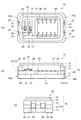
図1、および図2を用い、本発明の第1実施形態に係る電子デバイスについて説明する。図1は、本発明の第1実施形態に係る電子デバイスの概略を示し、(a)は蓋部材としてのリッドを省略した平面図であり、(b)は正断面図であり、(c)は(b)を図示左側から見た左側面図である。図2は、第1実施形態に係る電子デバイスの製造方法の一例を示すフローチャートである。なお、以下の説明では、第1実施形態に係る電子デバイスとして、電子部品として音叉型の振動素子を備えた発振器を例に説明する。
<First Embodiment>
The electronic device according to the first embodiment of the present invention will be described with reference to FIGS. 1 and 2. FIG. 1 shows an outline of an electronic device according to a first embodiment of the present invention, (a) is a plan view in which a lid as a lid member is omitted, (b) is a front sectional view, and (c). FIG. 3B is a left side view of FIG. FIG. 2 is a flowchart showing an example of a method for manufacturing an electronic device according to the first embodiment. In the following description, as an electronic device according to the first embodiment, an oscillator including a tuning fork type vibration element as an electronic component will be described as an example.
図1(a)、(b)、(c)に示す第1実施形態に係る電子デバイスとしての発振器10は、音叉型の振動素子20と、振動素子20を駆動する機能を少なくとも有している回路素子35と、振動素子20および回路素子35を収納するパッケージ16とを有している。以下、それぞれの構成部位について順次詳細に説明する。
An
<パッケージ>
回路基板としてのパッケージ16は、底板11、底板11の表面周縁部に設けられている枠状の1層目の側壁としての第1側壁12、および第1側壁12の上面に設けられている枠状の2層目の側壁としての第2側壁13を含むベース基板45と、第2側壁13の上面に設けられている接合材としてのシームリング14と、シームリング14を介して第2側壁13と接合されている蓋部材としてのリッド15とを有している。パッケージ16は、振動素子20、回路素子35などを収納する収納容器としての機能を有している。
<Package>
A
回路基板としてのパッケージ16は、上面に開放する凹部(内部空間17)を有している。凹部の開口は、接合材としてのシームリング14を介して第2側壁13に接合されているリッド15によって塞がれている。そして、パッケージ16の凹部の開口が塞がれて密封された内部空間17が形成される。密封された内部空間17は、その内部圧力を所望の気圧に設定できる。例えば、内部空間17に窒素ガスを充填しての大気圧としたり、真空(通常の大気圧より低い圧力(1×10⁵Pa〜1×10⁻¹⁰Pa以下(JIS Z 8126−1:1999))の気体で満たされた空間の状態)としたりすることで、より安定した振動素子20の振動を継続することができる。なお、本実施形態の内部空間17は、音叉型の振動素子20を収納しているため、上記の真空に設定されている。
The
枠状の第1側壁12、および第2側壁13は、略矩形状の周状に設けられており、換言すれば、上記凹部の上面に開口する開口形状が略矩形状をなしている。第1側壁12は、第2側壁13よりパッケージ16の中心側、換言すれば内側に向いた側面を有する内端を有し、凹部内に段部を形成する部分を含んでいる。第1側壁12によって形成された段部には、PAD電極37、第1パッド30、第2パッド31などが設けられている。この板状の底板11と枠状の第1側壁12および第2側壁13に囲まれた凹部が振動素子20、回路素子35などを収納する内部空間(収納空間)17となる。枠状の第2側壁13の上面には、例えばコバール等の合金で形成されたシームリング14が設けられている。シームリング14は、リッド15と第2側壁13との接合材としての機能を有しており、第2側壁13の上面に沿って枠状(略矩形状の周状)に設けられている。
The frame-like
ベース基板45は、振動素子20やリッド15の熱膨張係数と一致、あるいは極力近い熱膨張係数を備えた材料によって形成され、本例では、セラミックを用いている。ベース基板45は、所定の形状に成形されたグリーンシートを積層し、焼結することによって形成される。なお、グリーンシートは、例えば所定の溶液中にセラミックのパウダーを分散させ、バインダーを添加して生成される混練物がシート状に形成された物である。
The
第1側壁12の段部には、複数のPAD電極37、第1パッド30、第2パッド31などが形成されている。複数のPAD電極37、第1パッド30、第2パッド31は、例えば、銀・パラジウム合金などの導電ペーストあるいはタングステンメタライズなどを用い、必要とされる形状を形成後に焼成を行い、その後ニッケル(Ni)、金(Au)、あるいは銀(Ag)などをメッキすることによって形成される。第1パッド30、および第2パッド31は、振動素子20の支持腕18,19のそれぞれに設けられている第1接続電極(不図示)、第2接続電極(不図示)と接続されている。第1パッド30は、配線32を介してベース基板45の第1側面45aの第1凹部25に設けられている第1端子21と電気的に接続されている。第2パッド31は、配線33を介してベース基板45の第1側面45aの第2凹部26に設けられている第2端子22と電気的に接続されている。したがって、振動素子20の一方の励振電極(不図示)は、第1接続電極、第1パッド30、および配線32を介して第1端子21と電気的に接続されている。また、振動素子20の他方の励振電極(不図示)は、第2接続電極、第2パッド31、および配線33を介して第2端子22と電気的に接続されている。複数のPAD電極37は、図示しない配線を介していずれかの外部接続端子40と電気的に接続されている。なお、配線32,33は、前述のPAD電極37などと同様に形成することができる。
A plurality of
前述のように、振動素子20は、この段部に設けられた第1パッド30および第2パッド31に、支持腕18,19のそれぞれに設けられている第1接続電極(不図示)、第2接続電極(不図示)が、導電性接着剤19などの接続材で電気的な接続を取って接着されている。また、後述する回路素子35は、底板11上に樹脂系の接着剤(図示せず)などで接着されている。
As described above, the
ベース基板45の短辺側の2つの側面(第1側面45a、第2側面45b)には、第2側壁13の頂面から底板11に達する凹部(キャスタレーション)が第1側面45aおよび第2側面45bのそれぞれに、2つずつ設けられている。振動素子20が配置されている側の第1側面45aには、第1凹部25と第2凹部26とが設けられている。また、第1凹部25と第2凹部26が設けられている第1側面45aと対向する側の第2側面45b、即ち回路素子35が設けられている側の第2側面45bには第3凹部27と第4凹部28とが設けられている。第1側壁12および第2側壁13にかかる第1凹部25の内壁には、第1端子21が設けられている。また、第1側壁12および第2側壁13にかかる第2凹部26の内壁には、第2端子22が設けられている。前述のように、第1端子21は、配線32を介して第1パッド30と接続されており、第2端子22は配線33を介して第2パッド31と接続されている。
On the two side surfaces (
また、第1側壁12および第2側壁13にかかる第3凹部27の内壁には、第3端子23が設けられている。また、第1側壁12および第2側壁13にかかる第4凹部28の内壁には、第4端子24が設けられている。なお、第1端子21と第4端子24とは、ベース基板45の平面視での中心を基準にして点対称の位置に配置されている。また、第2端子22と第3端子23とは、ベース基板45の平面視での中心を基準にして点対称の位置に配置されている。このように、第1端子21〜第4端子24の4つの端子が配置されることにより、パッケージ16の向きが逆になっても同じ位置に端子が配置されるため、いずれの向きでも同じ位置で端子に測定端子(ピンプローブ)などを当接させることができる。
In addition, a
そして、第3端子23と第4端子24とは、第1側壁12と第2側壁13との間に設けられている接続配線34によって電気的に接続されている。換言すれば、第3端子23と第4端子24とは、電気的に短絡されている。接続配線34は、タングステンメタライズなどを用い、必要とされる形状を形成後に焼成を行うことで形成される。タングステンの電気抵抗率は、53nΩ・m程度であり、タングステンを用いた接続配線34であれば、第3端子23と第4端子24との間の電気抵抗値は、接続配線34の長さに応じた所定の値を示すことになる。
The
このように、第3端子23と第4端子24との間に所定の電気的抵抗値を有していれば、第3端子23と第4端子24とに測定部としてのプローブなどを当接させて測定することにより、金などを用いた電気配線や振動素子20の電極などの短絡と電気的抵抗値が異なるため、電気配線や振動素子20の電極などの短絡を判別することが可能となる。換言すれば、第1端子21と第2端子22間の短絡における電気的抵抗値と、第3端子23と第4端子24間の電気的抵抗値を比較することにより、第1端子21と第2端子22の側、あるいは第3端子23と第4端子24の側の、いずれの側がプローブに向いているかを判別することができる。これにより、パッケージ16の向きを判別することができる。
As described above, if a predetermined electrical resistance value is provided between the
また、第3端子23と第4端子24とを、PAD電極37内の一の端子(第5端子)38と電気的に接続させることにより、上述と同様に、第1端子21と第2端子22の側、あるいは第3端子23と第4端子24の側の、いずれの側がプローブに向いているかを判別することができる。即ち、第1端子21と第2端子22の電位と、第3端子23と第4端子24の電位を比較することにより、第1端子21と第2端子22の側、あるいは第3端子23と第4端子24の側の、いずれの側がプローブに向いているかを判別することができる。なお、一の端子(第5端子)38が、GND端子であれば、電位が安定しており、確実な確認(判定)を行うことに好適である。
In addition, by electrically connecting the
上述のように、ベース基板45の第1側面45aに設けられている第1凹部25および第2凹部26の内壁に第1端子21および第2端子22が備えられ、ベース基板45の第2側面45bに設けられている第3凹部27および第4凹部28との内壁に第3端子23、および第4端子24が備えられている。これにより、振動素子20の測定をパッケージ16の側面側から行うことができ、測定を行いながらパッケージ16の平面側(凹部の開口側)からの加工を行うことが可能となる。
As described above, the
なお、本形態では、第1凹部25に第1端子21が設けられ、第2凹部26に第2端子22が設けられているように、一つの凹部に一つの端子が設けられている例で説明したが、一つの凹部に複数の端子が設けられている構成でもよい。また、本形態では、パッケージの一辺に2つの端子(第1端子21と第2端子22、第3端子23と第4端子24)が設けられている例で説明したが、端子の数は二つ以上であれば数は問わない。
In this embodiment, the
リッド15は、板状の部材であり、パッケージ16の上面に開放する凹部の開口を塞ぎ、凹部の開口の周囲を、例えばシーム溶接法などを用いて接合されている。本例のリッド15は、板状であるため、形成が行い易く、さらには形状の安定性にも優れる。また、本例のリッド15には、コバールの板材が用いられている。リッド15にコバールの板材を用いることで封止の際に、コバールで形成されているシームリング14とリッド15とが同じ溶融状態で溶融され、さらには合金化もされ易いため、封止を容易に、かつ確実に行うことができる。なお、リッド15には、コバールに換えて他の材料の板材を用いてもよく、例えば、42アロイ、ステンレス鋼などの金属材料、またはパッケージ16の第2側壁13と同材料などを用いることができる。
The
(回路素子)
回路素子35は、底板11上に配置され、底板11に樹脂系の接着剤などによって接続されている。回路素子35は、例えば振動素子20を発振させる発振回路などを備えている。回路素子35の能動面には図示しない電極パッドが設けられており、この電極パッドと、ベース基板45を構成する第1側壁12の段部に設けられているPAD電極37とが、金属配線(ボンディングワイヤー)36によって電気的導通をとって接続されている。
(Circuit element)
The
(発振器の製造方法)
次に、図2に示すフローチャートを参照して、前述した構成の第1実施形態に係る電子デバイスとしての発振器10の製造方法について説明する。なお、発振器10の構成については、図1も参照しながら説明する。
(Oscillator manufacturing method)
Next, a method for manufacturing the
先ず、図1に示すような、上面に開放する凹部(内部空間17)を有しているパッケージ16を用意する。そして、第1パッド30、および第2パッド31に音叉型の振動素子20を接続する。振動素子20は、一方の支持腕18を第1パッド30に接続し、他方の支持腕19を第2パッド31に導電性接着剤29を用い、電気的接続をとって接続する。
First, as shown in FIG. 1, a
次に、振動素子20の特性測定を行う測定部としての2つのピンプローブを備えた測定装置により、パッケージ16に接続された振動素子20の特性測定を行う。この測定工程について、フローチャートを参照して説明する。
Next, the characteristic measurement of the
先ず、測定部としての2つのピンプローブをベース基板45の一方の側面に設けられた2つの端子に当接させ、振動素子20の特性を測定する(第1の測定工程:ステップS101)。ここで、2つのピンプローブは、パッケージ16の配置方向によって、第1端子21および第2端子22、または第3端子23および第4端子24のいずれか一対に当接する。そして測定信号を印加することによって振動素子20を振動させ、その特性を測定し、良否判定を行う(第1確認工程:ステップS103)。
First, two pin probes as measurement units are brought into contact with two terminals provided on one side surface of the
この測定により、特性が「良:OK」(ステップS103:Yes)と判定されれば、振動素子20は「良品」とされて、測定工程は終了する。この場合は、第1端子21と第2端子22とに、ピンプローブが当接していることになる。
If the characteristic is determined to be “good: OK” (step S103: Yes) by this measurement, the
第1確認工程(ステップS103)により、特性が「否:NG」(ステップS103:No)と判定された場合は、次の第2確認工程(ステップS105)により測定している端子間が所望の導通状態(例えば、ショート(短絡))であるか否かを判定する。この測定では、ピンプローブが当接している2つの端子間の電気的抵抗値を測定し、第3端子23と第4端子24との間のように所定の電気的抵抗値を持っているか否かも併せて測定する。
If the characteristic is determined to be “No: NG” (Step S103: No) in the first confirmation step (Step S103), the desired distance between the terminals measured in the second confirmation step (Step S105) is desired. It is determined whether or not it is in a conductive state (for example, short (short circuit)). In this measurement, the electrical resistance value between the two terminals in contact with the pin probe is measured, and whether or not the electrical resistance value has a predetermined electrical resistance value between the
そして、所定の電気的抵抗値を持った接続状態(例えば、ショート(短絡))と判定された場合(ステップS105:Yes)は、第3端子23と第4端子24とにピンプローブが当接している、即ちパッケージの向きが逆向きとなっていると判定し、パッケージ16の向きを反転させて、再度の特性測定を行う(第2の測定工程:ステップS107)。また、第2判定工程(ステップS105)の測定により、特性が「否:NG」(ステップS105:No)と判定された場合は、振動素子20の不良と判定する。この場合には、所定の電気的抵抗値以外の電気的抵抗値を持ったショート(短絡)も、振動素子20、配線32,33などを含む不良と判定し、測定工程を終了する。
When it is determined that the connection state has a predetermined electrical resistance value (for example, short circuit) (step S105: Yes), the pin probe comes into contact with the
第2の測定工程(ステップS107)において、特性が「否:NG」(ステップS107:No)と判定された場合は、振動素子20の不良と判定する。また、第2の測定工程(ステップS107)において、特性が「良:OK」(ステップS107:Yes)と判定されれば、振動素子20は「良品」とされて、一連の測定工程は終了する。
In the second measurement step (step S107), when the characteristic is determined as “No: NG” (step S107: No), it is determined that the
このような一連の測定工程とすることで、第1の測定工程(ステップS101)と第1判定工程(ステップS103)とで電子部品としての振動素子20の不具合か、電子デバイスとしての発振器10の向きの不整合かを見極める。そして、発振器10の向きが不整合の場合は、向きを正した(逆向きにする)後に第2の測定工程(ステップS107)で再測定を行うことで測定を終了させることができる。このように、効率よく測定することができる。
By adopting such a series of measurement steps, the first measurement step (step S101) and the first determination step (step S103) may be a failure of the
次に、振動素子20が良品と判定されたパッケージ16の凹部の底板11に回路素子35を接着剤(図示せず)によって固定する。その後、回路素子35の能動面に設けられている図示しない電極パッドと、パッケージ16を構成する第1側壁12の段部に設けられているPAD電極37とを、金属配線(ボンディングワイヤー)36によって接続する。
Next, the
次に、振動素子20の周波数調整を行った後、シームリング14を介してリッド15を、例えばシーム溶接法を用いて第2側壁13に接合する。これにより、パッケージ16の凹部の開口が塞がれ、密封された内部空間17が形成される。密封された内部空間17は、真空(通常の大気圧より低い圧力(1×10⁵Pa〜1×10⁻¹⁰Pa以下(JIS Z 8126−1:1999))の気体で満たされた空間の状態)とする。
Next, after adjusting the frequency of the
次に、発振器10の電気特性検査を行い、良否判定することで発振器10の製造工程が終了し、発振器10が完成する。
Next, the electrical characteristics of the
上述の第1実施形態に係る電子デバイスとしての発振器10は、回路基板としてのパッケージ16の向き、即ち、発振器10の向きを一回の測定で確実に判別することができる。したがって、判定回数の少ない、即ち効率のよい判定により測定工数を削減することが可能な回路基板としてのパッケージ16、および電子デバイスとしての発振器10を提供することができる。
The
<第2実施形態>
次に、図3を用い、本発明の第2実施形態に係る電子デバイスについて説明する。図3は、本発明の第2実施形態に係る電子デバイスの概略を示し、(a)は蓋部材としてのリッドを省略した平面図であり、(b)は正断面図であり、(c)は(b)を図示左側から見た左側面図である。なお、以下の説明では、第2実施形態に係る電子デバイスとして、電子部品として音叉型の振動素子を備えた発振器を例に説明する。また、前述の第1実施形態の発振器10と同様な構成については同符号を付してその説明を省略する。
Second Embodiment
Next, an electronic device according to a second embodiment of the present invention will be described using FIG. FIG. 3 shows an outline of an electronic device according to a second embodiment of the present invention, wherein (a) is a plan view in which a lid as a lid member is omitted, (b) is a front sectional view, and (c). FIG. 3B is a left side view of FIG. In the following description, as an electronic device according to the second embodiment, an oscillator including a tuning fork type vibration element as an electronic component will be described as an example. Further, the same components as those of the
(発振器)
図3(a)、(b)、(c)に示す第2実施形態に係る電子デバイスとしての発振器50は、振動素子20と、振動素子20を駆動する機能を少なくとも有している回路素子35と、振動素子20および回路素子35を収納するパッケージ117とを有している。発振器50は、前述の第1実施形態に係る電子デバイスとしての発振器10と比し、振動素子20および回路素子35の配設位置が異なる。以下では、第1実施形態と異なる構成のパッケージ117を中心に説明し、同様な構成の振動素子20、および回路素子35は同符号を付して説明を省略する。また、パッケージ117を構成するシームリング115、およびリッド116については、第1実施形態と同様な構成であるので詳細な説明を省略する。
(Oscillator)
An
<パッケージ>
図3(a)、(b)、(c)に示す、回路基板としてのパッケージ117は、底板111、底板111の一方面の周縁部に設けられている枠状の第1側壁112、底板111の他方面(裏面)の周縁部に設けられている枠状の第2側壁113、および第2側壁113に重ねて設けられている枠状の第3側壁114を含むベース基板145と、第1側壁112の上面に設けられている接合材としてのシームリング115、シームリング115を介して第1側壁112と接合されている蓋部材としてのリッド116とを有している。
<Package>
A
回路基板としてのパッケージ117は、上面に開放する凹部(内部空間139)と、下面に開放する凹部150とを有している。内部空間139の開口は、接合材としてのシームリング115を介して第1側壁112に接合されているリッド116によって密封されている。そして、密封された内部空間139は、その内部圧力を所望の気圧に設定できる。例えば、内部空間139に窒素ガスを充填しての大気圧としたり、真空(通常の大気圧より低い圧力(1×10⁵Pa〜1×10⁻¹⁰Pa以下(JIS Z 8126−1:1999))の気体で満たされた空間の状態)としたりすることで、より安定した振動素子20の振動を継続することができる。なお、本実施形態の内部空間139は、音叉型の振動素子20を収納しているため、上記の真空に設定されている。また、内部空間139と底板111を挟んだ反対側には、下面に開放する凹部150が設けられている。この凹部150には、回路素子35が収納されている。
The
枠状の第1側壁112は、略矩形状の周状に設けられており、換言すれば、上記凹部の上面に開口する開口形状が略矩形状をなしている。そして、底板111と枠状の第1側壁112に囲まれた凹部が振動素子20を収納する内部空間(収納空間)139となる。底板111の上面には、第1パッド130と第2パッド131とが設けられている。第1パッド130と第2パッド131とは、振動素子20を接続するための端子であり、第1パッド130には、振動素子20の支持腕118が導電性接着剤129によって接続され、第2パッド131には、振動素子20の支持腕119が導電性接着剤129によって接続されている。このように、振動素子20が、内部空間139内の底板111に接続されている。枠状の第1側壁112の上面には、例えばコバール等の合金で形成されたシームリング115が設けられている。シームリング115は、リッド116と第1側壁112との接合材としての機能を有しており、第1側壁112の上面に沿って枠状(略矩形状の周状)に設けられている。
The frame-shaped
枠状の第2側壁113、および第3側壁114は、略矩形状の周状に設けられており、換言すれば、凹部150の開口形状が略矩形状をなしている。第2側壁113は、第3側壁114よりパッケージ117の中心側、換言すれば内側に向いた側面を有する内端を有し、凹部内に段部を形成する部分を含んでいる。第2側壁113によって形成された段部には、図示しないPAD電極などが設けられている。底板111と枠状の第2側壁113および第3側壁114に囲まれた凹部150が回路素子35を収納する空間となる。底板111の裏面には、回路素子35が接続されており、回路素子35の能動面に設けられている図示しない電極パッドと、第2側壁113の段部に設けられているPAD電極とが、金属配線(ボンディングワイヤー)136によって電気的導通をとって接続されている。凹部150に収納された回路素子35は、凹部150に注入された封止材138によって覆われて封止されている。
The frame-like
ベース基板145は、振動素子20やリッド116の熱膨張係数と一致、あるいは極力近い熱膨張係数を備えた材料によって形成され、本例では、セラミックを用いている。ベース基板145は、所定の形状に成形されたグリーンシートを積層し、焼結することによって形成される。なお、グリーンシートは、例えば所定の溶液中にセラミックのパウダーを分散させ、バインダーを添加して生成される混練物がシート状に形成された物である。
The
底板111の表面に設けられている第1パッド130、第2パッド131、および第2側壁113の段部に設けられている図示しない複数のPAD電極は、例えば、銀・パラジウム合金などの導電ペーストあるいはタングステンメタライズなどを用い、必要とされる形状を形成後に焼成を行い、その後ニッケル(Ni)、金(Au)、あるいは銀(Ag)などをメッキすることによって形成される。第1パッド130、および第2パッド131は、第1パッド130、および第2パッド131は、振動素子20の支持腕118,119のそれぞれに設けられている第1接続電極(不図示)、第2接続電極(不図示)と接続されている。第1パッド130は、配線132を介してベース基板145の第1側面145aの第1凹部125に設けられている第1端子121と電気的に接続されている。第2パッド131は、配線133を介してベース基板145の第1側面145aの第2凹部126に設けられている第2端子122と電気的に接続されている。したがって、振動素子20の一方の励振電極(不図示)は、第1接続電極、第1パッド130、および配線132を介して第1端子121と電気的に接続されている。また、振動素子20の他方の励振電極(不図示)は、第2接続電極、第2パッド131、および配線133を介して第2端子122と電気的に接続されている。複数のPAD電極は、図示しない配線を介していずれかの外部接続端子140と電気的に接続されている。なお、配線132,133は、前述の第1パッド130などと同様に形成することができる。
The plurality of PAD electrodes (not shown) provided on the
ベース基板145の短辺側の2側面(第1側面145a、第2側面145b)には、第1側壁112の頂面から第3側壁114の下面に達する凹部(キャスタレーション)が、それぞれの辺に2つずつ設けられている。一方の第1側面145aには、第1凹部125と第2凹部126とが設けられている。また、第1凹部125と第2凹部126が設けられている第1側面145aと対向する側の第2側面145bには、第3凹部127と第4凹部128とが設けられている。底板111および第1側壁112にかかる第1凹部125の内壁には、第1端子121が設けられている。また、底板111および第1側壁112にかかる第2凹部126の内壁には、第2端子122が設けられている。前述のように、第1端子121は、配線132を介して第1パッド130と接続されており、第2端子122は配線133を介して第2パッド131と接続されている。
On the two side surfaces (the
また、底板111および第1側壁112にかかる第3凹部127の内壁には、第3端子123が設けられている。また、底板111および第1側壁112にかかる第4凹部128の内壁には、第4端子124が設けられている。なお、第1端子121と第4端子124とは、ベース基板145の平面視での中心を基準にして点対称の位置に配置されている。また、第2端子122と第3端子123とは、ベース基板145の平面視での中心を基準にして点対称の位置に配置されている。このように、第1端子121〜第4端子124の4つの端子が配置されることにより、パッケージ117の向きが逆になっても同じ位置に端子が配置されるため、いずれの向きでも同じ位置で端子に測定端子(ピンプローブ)などを当接させることができる。
In addition, a
そして、第3端子123と第4端子124とは、底板111と第1側壁112との間に設けられている接続配線134によって電気的に接続されている。換言すれば、第3端子123と第4端子124とは、電気的に短絡されている。接続配線134は、タングステンメタライズなどを用い、必要とされる形状を形成後に焼成を行うことで形成される。タングステンの電気抵抗率は、53nΩ・m程度であり、タングステンを用いた接続配線134であれば、第3端子123と第4端子124との間の電気抵抗値は、接続配線134の長さに応じた所定の値を示すことになる。
The
このように、第3端子123と第4端子124との間に所定の電気的抵抗値を有していれば、第3端子123と第4端子124とに測定部としてのプローブなどを当接させて測定することにより、金などを用いた電気配線や振動素子20の電極などの短絡と電気的抵抗値が異なるため、電気配線や振動素子20の電極などの短絡を判別することが可能となる。換言すれば、第1端子121と第2端子122間の短絡における電気的抵抗値と、第3端子123と第4端子124間の電気的抵抗値を比較することにより、第1端子121と第2端子122の側、あるいは第3端子123と第4端子124の側の、いずれの側がプローブに向いているかを判別することができる。これにより、パッケージ117の向きを判別することができる。
As described above, if a predetermined electrical resistance value is provided between the
また、第3端子123と第4端子124とを、GND端子と電気的に接続させることにより、上述と同様に第1端子121と第2端子122の側、あるいは第3端子123と第4端子124の側の、いずれの側がプローブに向いているかを判別することができる。即ち、第1端子121と第2端子122の電位と、第3端子123と第4端子124の電位を比較することにより、第1端子121と第2端子122の側、および第3端子123と第4端子124の側の、いずれの側がプローブに向いているかを判別することができる。
In addition, by electrically connecting the
上述のように、ベース基板145の第1側面145aに設けられている第1凹部125および第2凹部126の内壁に第1端子121および第2端子122が備えられ、ベース基板145の第2側面145bに設けられている第3凹部127および第4凹部128との内壁に第3端子123、および第4端子124が備えられている。これにより、振動素子20の測定をパッケージ117の側面側から行うことができ、測定を行いながらパッケージ117の平面側(凹部の開口側)からの加工を行うことが可能となる。
As described above, the
なお、本形態では、第1凹部125に第1端子121が設けられ、第2凹部126に第2端子122が設けられているように、一つの凹部に一つの端子が設けられている例で説明したが、一つの凹部に複数の端子が設けられている構成でもよい。また、本形態では、パッケージの一辺に2つの端子(第1端子121と第2端子122、第3端子123と第4端子124)が設けられている例で説明したが、端子の数は二つ以上であれば数は問わない。
In this embodiment, the
(発振器の製造方法)
発振器50の製造方法は、前述した第1実施形態に係る発振器10の製造方法と比べ、回路素子35の接続位置と封止方法が異なるが、前述の第1実施形態でフローチャートを用いて説明した振動素子20の特性測定の工程については同じ工程であるため説明を省略する。
(Oscillator manufacturing method)
The manufacturing method of the
上述の第2実施形態に係る電子デバイスとしての発振器50は、回路基板としてのパッケージ117の向き、即ち、発振器50の向きを一回の測定で確実に判別することができる。したがって、判定回数の少ない、即ち効率のよい判定により測定工数を削減することが可能な回路基板としてのパッケージ117、および電子デバイスとしての発振器50を提供することができる。
The
また、上述の第1実施形態、および第2実施形態では、ベース基板45,145を構成する材料として、セラミック基板を一例として説明したがこれに限らず、例えば水晶基板、ガラス基板、シリコン基板などを用いることも可能である。
In the first embodiment and the second embodiment described above, the ceramic substrate has been described as an example of the material constituting the
また、上述の第1実施形態、および第2実施形態では、パッケージ16,117の封止を、シームリング14,115を介して蓋体としてのリッド15,116を第2側壁13あるいは第1側壁112に接合する構成で説明したがこれに限らない。気密に封止することが可能であれば構成は問わず、例えば、凹状の内部空間を形成された金属キャップを用い、セラミック基板上に金属キャップをシーム溶接法などにより接合する構成などであってもよい。
In the first and second embodiments described above, the
また、上述の第1実施形態、および第2実施形態では電子デバイスの一例として音叉型の振動素子を備えた発振器を用いて説明したがこれに限らない。例えば、ATカット、あるいはCTカットなど他の形態の振動素子を収納した振動子や発振器、振動素子に替えて加速度、角速度、圧力などを測定可能なセンサー素子を収納したセンサーデバイス、あるいは回路素子を収納した半導体装置なども適用可能である。 In the first and second embodiments described above, the description has been given using the oscillator including the tuning fork type vibration element as an example of the electronic device, but the present invention is not limited thereto. For example, a vibrator or oscillator containing another form of vibration element such as AT cut or CT cut, a sensor device containing a sensor element capable of measuring acceleration, angular velocity, pressure, etc., or a circuit element instead of the vibration element A housed semiconductor device or the like is also applicable.
[電子機器]
次いで、本発明の一実施形態に係る電子デバイスとして、回路基板としてのパッケージ16を用いた発振器10、あるいは回路基板としてのパッケージ117を用いた発振器50のいずれかを適用した電子機器について、図4〜図6に基づき、詳細に説明する。なお、説明では、発振器10を適用した例を示している。
[Electronics]
Next, as an electronic device according to an embodiment of the present invention, an electronic apparatus to which either the
図4は、本発明の一実施形態に係る電子デバイスとしての発振器10を備える電子機器としてのモバイル型(またはノート型)のパーソナルコンピューターの構成の概略を示す斜視図である。この図において、パーソナルコンピューター1100は、キーボード1102を備えた本体部1104と、表示部100を備えた表示ユニット1106とにより構成され、表示ユニット1106は、本体部1104に対しヒンジ構造部を介して回動可能に支持されている。このようなパーソナルコンピューター1100には、信号処理のタイミング源としての機能を備えた発振器10が内蔵されている。
FIG. 4 is a perspective view schematically illustrating the configuration of a mobile (or notebook) personal computer as an electronic apparatus including the
図5は、本発明の一実施形態に係る電子デバイスとしての発振器10を備える電子機器としての携帯電話機(PHSも含む)の構成の概略を示す斜視図である。この図において、携帯電話機1200は、複数の操作ボタン1202、受話口1204および送話口1206を備え、操作ボタン1202と受話口1204との間には、表示部100が配置されている。このような携帯電話機1200には、信号処理のタイミング源としての機能を備えた発振器10が内蔵されている。
FIG. 5 is a perspective view schematically showing a configuration of a mobile phone (including PHS) as an electronic apparatus including the
図6は、本発明の一実施形態に係る電子デバイスとしての発振器10を備える電子機器としてのデジタルスチールカメラの構成の概略を示す斜視図である。なお、この図には、外部機器との接続についても簡易的に示されている。ここで、従来のフィルムカメラは、被写体の光像により銀塩写真フィルムを感光するのに対し、デジタルスチールカメラ1300は、被写体の光像をCCD(Charge Coupled Device)等の撮像素子により光電変換して撮像信号(画像信号)を生成する。
FIG. 6 is a perspective view schematically illustrating a configuration of a digital still camera as an electronic apparatus including the
デジタルスチールカメラ1300におけるケース(ボディー)1302の背面には、表示部100が設けられ、CCDによる撮像信号に基づいて表示を行う構成になっており、表示部100は、被写体を電子画像として表示するファインダーとして機能する。また、ケース1302の正面側(図中裏面側)には、光学レンズ(撮像光学系)やCCD等を含む受光ユニット1304が設けられている。
A
撮影者が表示部100に表示された被写体像を確認し、シャッターボタン1306を押下すると、その時点におけるCCDの撮像信号が、メモリー1308に転送、格納される。また、このデジタルスチールカメラ1300においては、ケース1302の側面に、ビデオ信号出力端子1312と、データ通信用の入出力端子1314とが設けられている。そして、図示されるように、ビデオ信号出力端子1312にはテレビモニター1430が、データ通信用の入出力端子1314にはパーソナルコンピューター1440が、それぞれ必要に応じて接続される。さらに、所定の操作により、メモリー1308に格納された撮像信号が、テレビモニター1430や、パーソナルコンピューター1440に出力される構成になっている。このようなデジタルスチールカメラ1300には、信号処理のタイミング源としての機能を備えた発振器10が内蔵されている。
When the photographer confirms the subject image displayed on the
なお、本発明の一実施形態に係る電子デバイスとしての発振器10は、図4のパーソナルコンピューター(モバイル型パーソナルコンピューター)、図5の携帯電話機、図6のデジタルスチールカメラの他にも、例えば、インクジェット式吐出装置(例えばインクジェットプリンター)、ラップトップ型パーソナルコンピューター、テレビ、ビデオカメラ、ビデオテープレコーダー、カーナビゲーション装置、ページャー、電子手帳(通信機能付も含む)、電子辞書、電卓、電子ゲーム機器、ワードプロセッサー、ワークステーション、テレビ電話、防犯用テレビモニター、電子双眼鏡、POS端末、医療機器(例えば電子体温計、血圧計、血糖計、心電図計測装置、超音波診断装置、電子内視鏡)、魚群探知機、各種測定機器、計器類(例えば、車両、航空機、船舶の計器類)、フライトシミュレーター等の電子機器に適用することができる。
The
[移動体]
図7は移動体の一例としての自動車を概略的に示す斜視図である。自動車506には本発明に係る電子デバイスとしての発振器10が搭載されている。例えば、同図に示すように、移動体としての自動車506には、発振器10を内蔵してタイヤ509などを制御する電子制御ユニット508が車体507に搭載されている。また、発振器10は、他にもキーレスエントリー、イモビライザー、カーナビゲーションシステム、カーエアコン、アンチロックブレーキシステム(ABS)、エアバック、タイヤ・プレッシャー・モニタリング・システム(TPMS:Tire Pressure Monitoring System)、エンジンコントロール、ハイブリッド自動車や電気自動車の電池モニター、車体姿勢制御システム、等の電子制御ユニット(ECU:electronic control unit)に広く適用できる。
[Moving object]
FIG. 7 is a perspective view schematically showing an automobile as an example of a moving body. The automobile 506 is equipped with an
10,50…電子デバイスとしての発振器、11…底板、12…第1側壁、13…第2側壁、14…シームリング、15…リッド、16…パッケージ、17…内部空間(凹部)、18,19…支持腕、20…振動素子、21…第1端子、22…第2端子、23…第3端子、24…第4端子、25…第1凹部、26…第2凹部、27…第3凹部、28…第4凹部、29…導電性接着剤、30…第1パッド、31…第2パッド、32…配線、33…配線、34…接続配線、35…回路素子、36…金属配線(ボンディングワイヤー)、37…PAD電極、38…一の端子(第5端子)、40…外部接続端子、45…ベース基板、45a…ベース基板の第1側面、45b…ベース基板の第2側面、506…移動体としての自動車、1100…電子機器としてのモバイル型のパーソナルコンピューター、1200…電子機器としての携帯電話機、1300…電子機器としてのデジタルスチールカメラ。
DESCRIPTION OF
Claims (13)
前記振動素子が搭載されている一方の主面、前記一方の主面に対して裏面となる他方の主面、第1側面および前記第1側面の反対側の第2側面、を備えたベース基板、
前記一方の主面に設けられており、前記振動素子の前記第1接続端子と電気的に接続されている第1パッド、
前記振動素子の前記第2接続端子と電気的に接続されている第2パッド、
前記第1側面に設けられており、かつ前記第1パッドと電気的に接続されている第1端子、
前記第1側面に設けられており、かつ前記第2パッドと電気的に接続されている第2端子、
前記第2側面に設けられている第3端子および第4端子及び、
前記他方の主面に設けられている外部接続端子を備え、
前記ベース基板の中心を基準にして、前記第1端子と前記第4端子とは点対称の位置にあり、
前記ベース基板の中心を基準にして、前記第2端子と前記第3端子とは点対称の位置にあり、
前記第3端子と前記第4端子とは、前記振動素子と電気的に接続することなく、互いに電気的に接続されており、
前記第1端子、前記第2端子、前記第3端子および前記第4端子は、前記外部接続端子と電気的に接続されていない回路基板と、
前記外部接続端子と電気的に接続され、かつ前記回路基板に搭載されている回路素子と
、を含んでいることを特徴とする電子デバイス。 A vibration element including a first connection terminal and a second connection terminal ;
One main surface the transducer elements Ru Tei is mounted, the other main surface of the back surface with respect to the one principal surface, base provided with a second side, opposite the first side surface and the first side surface Board,
Wherein provided on one main surface, the first connection terminal electrically connected to the first pad Ru Tei of the vibrating element,
The second connection terminal electrically connected to Tei Ru second pad of the vibrating element,
The first is provided on a side surface, and the first pad and electrically connected to the first pin and,
The first is provided on a side surface, and the second pad and electrically connected to the second pin and,
The third terminal and the fourth terminal and is provided on the second side,
An external connection pin which is provided on the other main surface,
With respect to the center of the base substrate, the first terminal and the fourth terminal are in point-symmetric positions,
With respect to the center of the base substrate, the second terminal and the third terminal are in point-symmetric positions,
The third terminal and the fourth terminal are electrically connected to each other without being electrically connected to the vibration element ,
The first terminal, the second terminal, the third terminal, and the fourth terminal are circuit boards that are not electrically connected to the external connection terminals;
A circuit element electrically connected to the external connection terminal and mounted on the circuit board;
An electronic device comprising:
前記回路基板の前記第3端子と前記第4端子とが電気的に短絡されていることを特徴とする電子デバイス。 The electronic device according to claim 1.
Electronic device, characterized in that said third terminal and the fourth terminal of the circuit board is shorted Electrical.
前記回路基板の前記ベース基板には第5端子が設けられ、
前記第3端子および前記第4端子は、前記第5端子に電気的に接続されていることを特
徴とする電子デバイス。 The electronic device according to claim 1 or claim 2 ,
A fifth terminal is provided on the base substrate of the circuit board ;
The electronic device, wherein the third terminal and the fourth terminal are electrically connected to the fifth terminal.
前記回路基板の前記第5端子はGND端子であることを特徴とする電子デバイス。 The electronic device according to claim 3 .
The electronic device , wherein the fifth terminal of the circuit board is a GND terminal.
前記回路基板の前記第1端子および前記第2端子は、前記第1側面に備えられている第1凹部内に設けられており、
前記第3端子および前記第4端子は、前記第2側面に備えられている第2凹部内に設け
られていることを特徴とする電子デバイス。 The electronic device according to any one of claims 1 to 4 ,
The first terminal and the second terminal of the circuit board are provided in a first recess provided on the first side surface,
The third terminal and the fourth terminal, electronic devices that characterized in that provided in the second recess provided in the second side surface.
前記回路基板の前記ベース基板は平面視にて略矩形状であることを特徴とする電子デバイス。 The electronic device according to any one of claims 1 to 5,
The electronic device according to claim 1 , wherein the base substrate of the circuit board has a substantially rectangular shape in plan view.
前記回路基板の前記第1パッドと前記第1端子を電気的に接続する第1の接続配線と、前記第2パッドと前記第2端子を電気的に接続する第2の接続配線とが、前記ベース基板の前記一方の主面に配設されていることを特徴とする電子デバイス。A first connection wiring that electrically connects the first pad and the first terminal of the circuit board; and a second connection wiring that electrically connects the second pad and the second terminal; An electronic device is provided on the one main surface of the base substrate.
前記回路基板の前記第3端子および前記第4端子を電気的に接続する第3の接続配線は、前記ベース基板の前記一方の主面に配設されていることを特徴とする電子デバイス。An electronic device, wherein a third connection wiring for electrically connecting the third terminal and the fourth terminal of the circuit board is disposed on the one main surface of the base substrate.
前記回路基板は、前記ベース基板の前記一方の主面に重なる側壁部を有し、The circuit board has a side wall portion overlapping the one main surface of the base substrate,
前記第3の接続配線は、前記側壁部と平面視で重なることを特徴とする電子デバイス。 The electronic device according to claim 3, wherein the third connection wiring overlaps the side wall portion in a plan view.
前記電子部品が搭載されている一方の主面、前記一方の主面に対して裏面となる他方の主面、第1側面および前記第1側面の反対側の第2側面を備えたベース基板、
前記一方の主面に設けられており、前記電子部品の前記第1接続端子と電気的に接続されている第1パッド、
前記電子部品の前記第2接続端子と電気的に接続されている第2パッド、
前記第1側面に設けられており、かつ前記第1パッドと電気的に接続されている第1端子、
前記第1側面に設けられており、かつ前記第2パッドと電気的に接続されている第2端子、
前記第2側面に設けられている第3端子および第4端子及び、
前記他方の主面に設けられている外部接続端子を備え、
前記ベース基板の中心を基準にして、前記第1端子と前記第4端子とは点対称の位置にあり、
前記ベース基板の中心を基準にして、前記第2端子と前記第3端子とは点対称の位置にあり、
前記第3端子と前記第4端子とは、前記電子部品と電気的に接続することなく、互いに電気的に接続されており、
前記第1端子、前記第2端子、前記第3端子および前記第4端子は、前記外部接続端子と電気的に接続されていない回路基板と、
前記外部接続端子と電気的に接続され、かつ前記回路基板に搭載されている回路素子と、を備えている電子デバイスを準備する工程と、
前記第1端子と前記第2端子、または前記第3端子と前記第4端子のいずれか一対の端
子に測定部を当接させて特性を測定する第1測定工程と、
前記第1測定工程において、前記いずれか一対の端子間の導通状態を確認する確認工程
と、
前記確認工程で、所定の導通状態の場合は、前記第1端子と前記第2端子、および前記
第3端子と前記第4端子のうち、前記いずれか一対の端子と異なる他方の一対の端子に前
記測定部を当接させて特性を測定する第2測定工程と、を含むことを特徴とする電子デバ
イスの製造方法。 An electronic component comprising a first connection terminal and a second connection terminal;
The Tei Ru one main surface an electronic component is mounted, the other main surface of the back surface with respect to the one principal surface, base plate having a second side opposite the first side surface and the first side surface ,
Wherein provided on one main surface, the electronic component of the first connection terminal electrically connected to the first pad Ru Tei,
The electronic component of the second connecting terminal electrically connected to Tei Ru second pad,
The first is provided on a side surface, and the first pad and electrically connected to the first pin and,
The first is provided on a side surface, and the second pad and electrically connected to the second pin and,
The third terminal and the fourth terminal and is provided on the second side,
An external connection pin which is provided on the other main surface,
With respect to the center of the base substrate, the first terminal and the fourth terminal are in point-symmetric positions,
With respect to the center of the base substrate, the second terminal and the third terminal are in point-symmetric positions,
The third terminal and the fourth terminal are electrically connected to each other without being electrically connected to the electronic component,
The first terminal, the second terminal, the third terminal, and the fourth terminal are circuit boards that are not electrically connected to the external connection terminals;
Preparing an electronic device comprising: a circuit element electrically connected to the external connection terminal and mounted on the circuit board;
A first measurement step of measuring characteristics by bringing a measurement unit into contact with any one pair of the first terminal and the second terminal, or the third terminal and the fourth terminal;
In the first measurement step, a confirmation step for confirming a conduction state between the pair of terminals,
In the confirming step, when a predetermined conduction state is established, the first terminal and the second terminal, and the third terminal and the fourth terminal are connected to the other pair of terminals different from the one pair of terminals. A second measuring step of measuring characteristics by bringing the measuring unit into contact with each other.
記導通状態を確認する工程であることを特徴とする請求項10に記載の電子デバイスの製造方法。 The method of manufacturing an electronic device according to claim 10 , wherein the confirmation step is a step of confirming the conduction state by measuring an electrical resistance value between the pair of terminals.
Priority Applications (3)
| Application Number | Priority Date | Filing Date | Title |
|---|---|---|---|
| JP2013083822A JP6171516B2 (en) | 2013-04-12 | 2013-04-12 | Electronic device, method for manufacturing electronic device, electronic apparatus, and moving body |
| CN201410136425.5A CN104104358B (en) | 2013-04-12 | 2014-04-04 | Circuit substrate, electronic device and its manufacturing method, electronic equipment and moving body |
| US14/249,707 US9363895B2 (en) | 2013-04-12 | 2014-04-10 | Circuit substrate, electronic device, method of manufacturing electronic device, electronic apparatus, and moving object |
Applications Claiming Priority (1)
| Application Number | Priority Date | Filing Date | Title |
|---|---|---|---|
| JP2013083822A JP6171516B2 (en) | 2013-04-12 | 2013-04-12 | Electronic device, method for manufacturing electronic device, electronic apparatus, and moving body |
Publications (3)
| Publication Number | Publication Date |
|---|---|
| JP2014207314A JP2014207314A (en) | 2014-10-30 |
| JP2014207314A5 JP2014207314A5 (en) | 2016-05-26 |
| JP6171516B2 true JP6171516B2 (en) | 2017-08-02 |
Family
ID=51672212
Family Applications (1)
| Application Number | Title | Priority Date | Filing Date |
|---|---|---|---|
| JP2013083822A Active JP6171516B2 (en) | 2013-04-12 | 2013-04-12 | Electronic device, method for manufacturing electronic device, electronic apparatus, and moving body |
Country Status (3)
| Country | Link |
|---|---|
| US (1) | US9363895B2 (en) |
| JP (1) | JP6171516B2 (en) |
| CN (1) | CN104104358B (en) |
Families Citing this family (2)
| Publication number | Priority date | Publication date | Assignee | Title |
|---|---|---|---|---|
| US9641733B1 (en) * | 2013-10-28 | 2017-05-02 | Apple Inc. | Miniature camera plural image sensor arrangements |
| JP6769220B2 (en) * | 2016-10-03 | 2020-10-14 | セイコーエプソン株式会社 | Electronic component packages, oscillators, electronics, and mobiles |
Family Cites Families (18)
| Publication number | Priority date | Publication date | Assignee | Title |
|---|---|---|---|---|
| US5585687A (en) * | 1994-02-23 | 1996-12-17 | Citizen Watch Co., Ltd. | Piezolelectric oscillator |
| JP3577170B2 (en) * | 1996-08-05 | 2004-10-13 | 株式会社村田製作所 | Piezoelectric resonator, method of manufacturing the same, and electronic component using the same |
| JP2974622B2 (en) * | 1996-09-20 | 1999-11-10 | 松下電器産業株式会社 | Oscillator |
| JP3990679B2 (en) * | 1996-11-08 | 2007-10-17 | 株式会社リコー | Semiconductor device provided with circuit board for semiconductor mounting |
| JP2000277574A (en) * | 1999-03-23 | 2000-10-06 | Casio Comput Co Ltd | Lsi chip and its junction testing method |
| JP2002124829A (en) * | 2000-10-12 | 2002-04-26 | Murata Mfg Co Ltd | Oscillator and electronic device using the same |
| JP4692722B2 (en) * | 2004-01-29 | 2011-06-01 | セイコーエプソン株式会社 | Electronic component package and electronic component |
| JP4898937B2 (en) * | 2004-06-11 | 2012-03-21 | 日本特殊陶業株式会社 | Multi-piece wiring board and manufacturing method thereof |
| JP4784055B2 (en) * | 2004-08-11 | 2011-09-28 | 株式会社大真空 | Piezoelectric oscillator |
| JP4799984B2 (en) * | 2005-09-30 | 2011-10-26 | 日本電波工業株式会社 | Temperature-compensated crystal oscillator for surface mounting |
| JP2007142869A (en) | 2005-11-18 | 2007-06-07 | Nippon Dempa Kogyo Co Ltd | Temperature compensated crystal oscillator for surface mounting |
| US7378780B2 (en) | 2005-11-09 | 2008-05-27 | Nihon Dempa Kogyo Co., Ltd. | Surface mount type crystal oscillator |
| JP2010068061A (en) * | 2008-09-09 | 2010-03-25 | Nippon Dempa Kogyo Co Ltd | Surface-mounted crystal oscillator |
| JP5058321B2 (en) * | 2009-11-11 | 2012-10-24 | 日本電波工業株式会社 | Surface-mount crystal unit and method for manufacturing the same |
| JP5731880B2 (en) * | 2010-10-15 | 2015-06-10 | 日本電波工業株式会社 | Piezoelectric device and method for manufacturing piezoelectric device |
| JP5558321B2 (en) * | 2010-11-19 | 2014-07-23 | 京セラ株式会社 | Multiple wiring board |
| JP2012199861A (en) * | 2011-03-23 | 2012-10-18 | Nippon Dempa Kogyo Co Ltd | Crystal device and method for inspecting the same |
| JP2013172369A (en) * | 2012-02-22 | 2013-09-02 | Nippon Dempa Kogyo Co Ltd | Piezoelectric device and manufacturing method of the same |
-
2013
- 2013-04-12 JP JP2013083822A patent/JP6171516B2/en active Active
-
2014
- 2014-04-04 CN CN201410136425.5A patent/CN104104358B/en active Active
- 2014-04-10 US US14/249,707 patent/US9363895B2/en active Active
Also Published As
| Publication number | Publication date |
|---|---|
| US20140305687A1 (en) | 2014-10-16 |
| CN104104358B (en) | 2018-12-28 |
| JP2014207314A (en) | 2014-10-30 |
| US9363895B2 (en) | 2016-06-07 |
| CN104104358A (en) | 2014-10-15 |
Similar Documents
| Publication | Publication Date | Title |
|---|---|---|
| US9432026B2 (en) | Oscillator, electronic apparatus, and moving object | |
| US9350318B2 (en) | Method for manufacturing electronic device, cover body, electronic device, electronic apparatus, and moving object | |
| US9159905B2 (en) | Electronic device, electronic apparatus, mobile unit, and method of manufacturing electronic device | |
| JP6179155B2 (en) | Vibration device, electronic device, and moving object | |
| US20140306582A1 (en) | Electronic component, electronic apparatus, and moving object | |
| US9516773B2 (en) | Lid body, package, electronic apparatus, moving object, and method for manufacturing package | |
| JP2014053663A (en) | Electronic device, electronic apparatus, and moving body | |
| JP6171516B2 (en) | Electronic device, method for manufacturing electronic device, electronic apparatus, and moving body | |
| JP6805697B2 (en) | Electronic component packages, oscillators, electronics, and mobiles | |
| JP6175760B2 (en) | Electronic device package manufacturing method, electronic device manufacturing method, electronic device manufacturing method, and moving body manufacturing method | |
| US10027308B2 (en) | Vibration device, electronic apparatus, and mobile object | |
| JP2015088643A (en) | Manufacturing method of electronic device, electronic device, electronic apparatus, movable body and lid body | |
| US10381978B2 (en) | Electronic-component package, oscillator, electronic apparatus, and vehicle | |
| US20150116974A1 (en) | Method of manufacturing electronic device, electronic device, electronic apparatus, moving object, and lid body | |
| JP2018074012A (en) | Package for electronic device, electronic device, electronic apparatus, and movable body | |
| JP2014107317A (en) | Method of manufacturing package for electronic device, electronic device, electronic apparatus, and mobile | |
| US20150179919A1 (en) | Resonator device, electronic apparatus, and moving object | |
| JP2015041891A (en) | Sheet substrate, method for manufacturing electronic device, and method for inspecting electronic device | |
| US20200298350A1 (en) | Electronic device manufacturing method, electronic device, electronic apparatus, and vehicle | |
| JP2014107316A (en) | Lid, package, electronic device, mobile, and manufacturing method for mobile | |
| JP6493589B2 (en) | Package, electronic device, moving body, and manufacturing method of package | |
| JP6222327B2 (en) | Manufacturing method of electronic device | |
| JP2014199970A (en) | Electronic device, electronic apparatus, mobile object, and laminated sheet manufacturing method | |
| JP2014145701A (en) | Electronic device manufacturing method, electronic device, electronic apparatus and movable body | |
| JP2016004853A (en) | Circuit board, oscillator, electronic apparatus and mobile body |
Legal Events
| Date | Code | Title | Description |
|---|---|---|---|
| RD04 | Notification of resignation of power of attorney |
Free format text: JAPANESE INTERMEDIATE CODE: A7424 Effective date: 20150113 |
|
| A521 | Request for written amendment filed |
Free format text: JAPANESE INTERMEDIATE CODE: A523 Effective date: 20160404 |
|
| A621 | Written request for application examination |
Free format text: JAPANESE INTERMEDIATE CODE: A621 Effective date: 20160404 |
|
| RD04 | Notification of resignation of power of attorney |
Free format text: JAPANESE INTERMEDIATE CODE: A7424 Effective date: 20160617 |
|
| RD03 | Notification of appointment of power of attorney |
Free format text: JAPANESE INTERMEDIATE CODE: A7423 Effective date: 20160624 |
|
| A977 | Report on retrieval |
Free format text: JAPANESE INTERMEDIATE CODE: A971007 Effective date: 20170309 |
|
| A131 | Notification of reasons for refusal |
Free format text: JAPANESE INTERMEDIATE CODE: A131 Effective date: 20170314 |
|
| A521 | Request for written amendment filed |
Free format text: JAPANESE INTERMEDIATE CODE: A523 Effective date: 20170509 |
|
| TRDD | Decision of grant or rejection written | ||
| A01 | Written decision to grant a patent or to grant a registration (utility model) |
Free format text: JAPANESE INTERMEDIATE CODE: A01 Effective date: 20170606 |
|
| A61 | First payment of annual fees (during grant procedure) |
Free format text: JAPANESE INTERMEDIATE CODE: A61 Effective date: 20170619 |
|
| R150 | Certificate of patent or registration of utility model |
Ref document number: 6171516 Country of ref document: JP Free format text: JAPANESE INTERMEDIATE CODE: R150 |