JP6157100B2 - Semiconductor device - Google Patents
Semiconductor device Download PDFInfo
- Publication number
- JP6157100B2 JP6157100B2 JP2012272137A JP2012272137A JP6157100B2 JP 6157100 B2 JP6157100 B2 JP 6157100B2 JP 2012272137 A JP2012272137 A JP 2012272137A JP 2012272137 A JP2012272137 A JP 2012272137A JP 6157100 B2 JP6157100 B2 JP 6157100B2
- Authority
- JP
- Japan
- Prior art keywords
- semiconductor device
- seal ring
- tsv
- dielectric constant
- constant film
- Prior art date
- Legal status (The legal status is an assumption and is not a legal conclusion. Google has not performed a legal analysis and makes no representation as to the accuracy of the status listed.)
- Active
Links
Images


Classifications
-
- H—ELECTRICITY
- H01—ELECTRIC ELEMENTS
- H01L—SEMICONDUCTOR DEVICES NOT COVERED BY CLASS H10
- H01L23/00—Details of semiconductor or other solid state devices
- H01L23/58—Structural electrical arrangements for semiconductor devices not otherwise provided for, e.g. in combination with batteries
- H01L23/585—Structural electrical arrangements for semiconductor devices not otherwise provided for, e.g. in combination with batteries comprising conductive layers or plates or strips or rods or rings
-
- H—ELECTRICITY
- H01—ELECTRIC ELEMENTS
- H01L—SEMICONDUCTOR DEVICES NOT COVERED BY CLASS H10
- H01L23/00—Details of semiconductor or other solid state devices
- H01L23/48—Arrangements for conducting electric current to or from the solid state body in operation, e.g. leads, terminal arrangements ; Selection of materials therefor
- H01L23/481—Internal lead connections, e.g. via connections, feedthrough structures
-
- H—ELECTRICITY
- H01—ELECTRIC ELEMENTS
- H01L—SEMICONDUCTOR DEVICES NOT COVERED BY CLASS H10
- H01L23/00—Details of semiconductor or other solid state devices
- H01L23/52—Arrangements for conducting electric current within the device in operation from one component to another, i.e. interconnections, e.g. wires, lead frames
- H01L23/522—Arrangements for conducting electric current within the device in operation from one component to another, i.e. interconnections, e.g. wires, lead frames including external interconnections consisting of a multilayer structure of conductive and insulating layers inseparably formed on the semiconductor body
- H01L23/5226—Via connections in a multilevel interconnection structure
-
- H—ELECTRICITY
- H01—ELECTRIC ELEMENTS
- H01L—SEMICONDUCTOR DEVICES NOT COVERED BY CLASS H10
- H01L23/00—Details of semiconductor or other solid state devices
- H01L23/52—Arrangements for conducting electric current within the device in operation from one component to another, i.e. interconnections, e.g. wires, lead frames
- H01L23/522—Arrangements for conducting electric current within the device in operation from one component to another, i.e. interconnections, e.g. wires, lead frames including external interconnections consisting of a multilayer structure of conductive and insulating layers inseparably formed on the semiconductor body
- H01L23/528—Geometry or layout of the interconnection structure
-
- H—ELECTRICITY
- H01—ELECTRIC ELEMENTS
- H01L—SEMICONDUCTOR DEVICES NOT COVERED BY CLASS H10
- H01L23/00—Details of semiconductor or other solid state devices
- H01L23/52—Arrangements for conducting electric current within the device in operation from one component to another, i.e. interconnections, e.g. wires, lead frames
- H01L23/522—Arrangements for conducting electric current within the device in operation from one component to another, i.e. interconnections, e.g. wires, lead frames including external interconnections consisting of a multilayer structure of conductive and insulating layers inseparably formed on the semiconductor body
- H01L23/532—Arrangements for conducting electric current within the device in operation from one component to another, i.e. interconnections, e.g. wires, lead frames including external interconnections consisting of a multilayer structure of conductive and insulating layers inseparably formed on the semiconductor body characterised by the materials
- H01L23/53204—Conductive materials
- H01L23/53209—Conductive materials based on metals, e.g. alloys, metal silicides
- H01L23/53228—Conductive materials based on metals, e.g. alloys, metal silicides the principal metal being copper
-
- H—ELECTRICITY
- H01—ELECTRIC ELEMENTS
- H01L—SEMICONDUCTOR DEVICES NOT COVERED BY CLASS H10
- H01L24/00—Arrangements for connecting or disconnecting semiconductor or solid-state bodies; Methods or apparatus related thereto
- H01L24/01—Means for bonding being attached to, or being formed on, the surface to be connected, e.g. chip-to-package, die-attach, "first-level" interconnects; Manufacturing methods related thereto
- H01L24/02—Bonding areas ; Manufacturing methods related thereto
- H01L24/04—Structure, shape, material or disposition of the bonding areas prior to the connecting process
- H01L24/05—Structure, shape, material or disposition of the bonding areas prior to the connecting process of an individual bonding area
-
- H—ELECTRICITY
- H01—ELECTRIC ELEMENTS
- H01L—SEMICONDUCTOR DEVICES NOT COVERED BY CLASS H10
- H01L24/00—Arrangements for connecting or disconnecting semiconductor or solid-state bodies; Methods or apparatus related thereto
- H01L24/01—Means for bonding being attached to, or being formed on, the surface to be connected, e.g. chip-to-package, die-attach, "first-level" interconnects; Manufacturing methods related thereto
- H01L24/02—Bonding areas ; Manufacturing methods related thereto
- H01L24/04—Structure, shape, material or disposition of the bonding areas prior to the connecting process
- H01L24/06—Structure, shape, material or disposition of the bonding areas prior to the connecting process of a plurality of bonding areas
-
- H—ELECTRICITY
- H01—ELECTRIC ELEMENTS
- H01L—SEMICONDUCTOR DEVICES NOT COVERED BY CLASS H10
- H01L25/00—Assemblies consisting of a plurality of individual semiconductor or other solid state devices ; Multistep manufacturing processes thereof
- H01L25/03—Assemblies consisting of a plurality of individual semiconductor or other solid state devices ; Multistep manufacturing processes thereof all the devices being of a type provided for in the same subgroup of groups H01L27/00 - H01L33/00, or in a single subclass of H10K, H10N, e.g. assemblies of rectifier diodes
- H01L25/04—Assemblies consisting of a plurality of individual semiconductor or other solid state devices ; Multistep manufacturing processes thereof all the devices being of a type provided for in the same subgroup of groups H01L27/00 - H01L33/00, or in a single subclass of H10K, H10N, e.g. assemblies of rectifier diodes the devices not having separate containers
- H01L25/065—Assemblies consisting of a plurality of individual semiconductor or other solid state devices ; Multistep manufacturing processes thereof all the devices being of a type provided for in the same subgroup of groups H01L27/00 - H01L33/00, or in a single subclass of H10K, H10N, e.g. assemblies of rectifier diodes the devices not having separate containers the devices being of a type provided for in group H01L27/00
- H01L25/0657—Stacked arrangements of devices
-
- H—ELECTRICITY
- H01—ELECTRIC ELEMENTS
- H01L—SEMICONDUCTOR DEVICES NOT COVERED BY CLASS H10
- H01L2224/00—Indexing scheme for arrangements for connecting or disconnecting semiconductor or solid-state bodies and methods related thereto as covered by H01L24/00
- H01L2224/01—Means for bonding being attached to, or being formed on, the surface to be connected, e.g. chip-to-package, die-attach, "first-level" interconnects; Manufacturing methods related thereto
- H01L2224/02—Bonding areas; Manufacturing methods related thereto
- H01L2224/0212—Auxiliary members for bonding areas, e.g. spacers
- H01L2224/02122—Auxiliary members for bonding areas, e.g. spacers being formed on the semiconductor or solid-state body
- H01L2224/02163—Auxiliary members for bonding areas, e.g. spacers being formed on the semiconductor or solid-state body on the bonding area
- H01L2224/02165—Reinforcing structures
- H01L2224/02166—Collar structures
-
- H—ELECTRICITY
- H01—ELECTRIC ELEMENTS
- H01L—SEMICONDUCTOR DEVICES NOT COVERED BY CLASS H10
- H01L2224/00—Indexing scheme for arrangements for connecting or disconnecting semiconductor or solid-state bodies and methods related thereto as covered by H01L24/00
- H01L2224/01—Means for bonding being attached to, or being formed on, the surface to be connected, e.g. chip-to-package, die-attach, "first-level" interconnects; Manufacturing methods related thereto
- H01L2224/02—Bonding areas; Manufacturing methods related thereto
- H01L2224/04—Structure, shape, material or disposition of the bonding areas prior to the connecting process
- H01L2224/05—Structure, shape, material or disposition of the bonding areas prior to the connecting process of an individual bonding area
- H01L2224/0554—External layer
- H01L2224/0555—Shape
- H01L2224/05552—Shape in top view
- H01L2224/05553—Shape in top view being rectangular
-
- H—ELECTRICITY
- H01—ELECTRIC ELEMENTS
- H01L—SEMICONDUCTOR DEVICES NOT COVERED BY CLASS H10
- H01L2224/00—Indexing scheme for arrangements for connecting or disconnecting semiconductor or solid-state bodies and methods related thereto as covered by H01L24/00
- H01L2224/01—Means for bonding being attached to, or being formed on, the surface to be connected, e.g. chip-to-package, die-attach, "first-level" interconnects; Manufacturing methods related thereto
- H01L2224/02—Bonding areas; Manufacturing methods related thereto
- H01L2224/04—Structure, shape, material or disposition of the bonding areas prior to the connecting process
- H01L2224/05—Structure, shape, material or disposition of the bonding areas prior to the connecting process of an individual bonding area
- H01L2224/0554—External layer
- H01L2224/0556—Disposition
- H01L2224/05567—Disposition the external layer being at least partially embedded in the surface
-
- H—ELECTRICITY
- H01—ELECTRIC ELEMENTS
- H01L—SEMICONDUCTOR DEVICES NOT COVERED BY CLASS H10
- H01L2224/00—Indexing scheme for arrangements for connecting or disconnecting semiconductor or solid-state bodies and methods related thereto as covered by H01L24/00
- H01L2224/01—Means for bonding being attached to, or being formed on, the surface to be connected, e.g. chip-to-package, die-attach, "first-level" interconnects; Manufacturing methods related thereto
- H01L2224/02—Bonding areas; Manufacturing methods related thereto
- H01L2224/04—Structure, shape, material or disposition of the bonding areas prior to the connecting process
- H01L2224/05—Structure, shape, material or disposition of the bonding areas prior to the connecting process of an individual bonding area
- H01L2224/0554—External layer
- H01L2224/0556—Disposition
- H01L2224/0557—Disposition the external layer being disposed on a via connection of the semiconductor or solid-state body
-
- H—ELECTRICITY
- H01—ELECTRIC ELEMENTS
- H01L—SEMICONDUCTOR DEVICES NOT COVERED BY CLASS H10
- H01L2224/00—Indexing scheme for arrangements for connecting or disconnecting semiconductor or solid-state bodies and methods related thereto as covered by H01L24/00
- H01L2224/01—Means for bonding being attached to, or being formed on, the surface to be connected, e.g. chip-to-package, die-attach, "first-level" interconnects; Manufacturing methods related thereto
- H01L2224/02—Bonding areas; Manufacturing methods related thereto
- H01L2224/04—Structure, shape, material or disposition of the bonding areas prior to the connecting process
- H01L2224/05—Structure, shape, material or disposition of the bonding areas prior to the connecting process of an individual bonding area
- H01L2224/0554—External layer
- H01L2224/05599—Material
- H01L2224/056—Material with a principal constituent of the material being a metal or a metalloid, e.g. boron [B], silicon [Si], germanium [Ge], arsenic [As], antimony [Sb], tellurium [Te] and polonium [Po], and alloys thereof
- H01L2224/05617—Material with a principal constituent of the material being a metal or a metalloid, e.g. boron [B], silicon [Si], germanium [Ge], arsenic [As], antimony [Sb], tellurium [Te] and polonium [Po], and alloys thereof the principal constituent melting at a temperature of greater than or equal to 400°C and less than 950°C
- H01L2224/05624—Aluminium [Al] as principal constituent
-
- H—ELECTRICITY
- H01—ELECTRIC ELEMENTS
- H01L—SEMICONDUCTOR DEVICES NOT COVERED BY CLASS H10
- H01L2224/00—Indexing scheme for arrangements for connecting or disconnecting semiconductor or solid-state bodies and methods related thereto as covered by H01L24/00
- H01L2224/01—Means for bonding being attached to, or being formed on, the surface to be connected, e.g. chip-to-package, die-attach, "first-level" interconnects; Manufacturing methods related thereto
- H01L2224/02—Bonding areas; Manufacturing methods related thereto
- H01L2224/04—Structure, shape, material or disposition of the bonding areas prior to the connecting process
- H01L2224/06—Structure, shape, material or disposition of the bonding areas prior to the connecting process of a plurality of bonding areas
- H01L2224/061—Disposition
- H01L2224/0618—Disposition being disposed on at least two different sides of the body, e.g. dual array
- H01L2224/06181—On opposite sides of the body
-
- H—ELECTRICITY
- H01—ELECTRIC ELEMENTS
- H01L—SEMICONDUCTOR DEVICES NOT COVERED BY CLASS H10
- H01L2224/00—Indexing scheme for arrangements for connecting or disconnecting semiconductor or solid-state bodies and methods related thereto as covered by H01L24/00
- H01L2224/01—Means for bonding being attached to, or being formed on, the surface to be connected, e.g. chip-to-package, die-attach, "first-level" interconnects; Manufacturing methods related thereto
- H01L2224/02—Bonding areas; Manufacturing methods related thereto
- H01L2224/07—Structure, shape, material or disposition of the bonding areas after the connecting process
- H01L2224/08—Structure, shape, material or disposition of the bonding areas after the connecting process of an individual bonding area
- H01L2224/081—Disposition
- H01L2224/0812—Disposition the bonding area connecting directly to another bonding area, i.e. connectorless bonding, e.g. bumpless bonding
- H01L2224/08135—Disposition the bonding area connecting directly to another bonding area, i.e. connectorless bonding, e.g. bumpless bonding the bonding area connecting between different semiconductor or solid-state bodies, i.e. chip-to-chip
- H01L2224/08145—Disposition the bonding area connecting directly to another bonding area, i.e. connectorless bonding, e.g. bumpless bonding the bonding area connecting between different semiconductor or solid-state bodies, i.e. chip-to-chip the bodies being stacked
-
- H—ELECTRICITY
- H01—ELECTRIC ELEMENTS
- H01L—SEMICONDUCTOR DEVICES NOT COVERED BY CLASS H10
- H01L2225/00—Details relating to assemblies covered by the group H01L25/00 but not provided for in its subgroups
- H01L2225/03—All the devices being of a type provided for in the same subgroup of groups H01L27/00 - H01L33/648 and H10K99/00
- H01L2225/04—All the devices being of a type provided for in the same subgroup of groups H01L27/00 - H01L33/648 and H10K99/00 the devices not having separate containers
- H01L2225/065—All the devices being of a type provided for in the same subgroup of groups H01L27/00 - H01L33/648 and H10K99/00 the devices not having separate containers the devices being of a type provided for in group H01L27/00
- H01L2225/06503—Stacked arrangements of devices
- H01L2225/06513—Bump or bump-like direct electrical connections between devices, e.g. flip-chip connection, solder bumps
-
- H—ELECTRICITY
- H01—ELECTRIC ELEMENTS
- H01L—SEMICONDUCTOR DEVICES NOT COVERED BY CLASS H10
- H01L2225/00—Details relating to assemblies covered by the group H01L25/00 but not provided for in its subgroups
- H01L2225/03—All the devices being of a type provided for in the same subgroup of groups H01L27/00 - H01L33/648 and H10K99/00
- H01L2225/04—All the devices being of a type provided for in the same subgroup of groups H01L27/00 - H01L33/648 and H10K99/00 the devices not having separate containers
- H01L2225/065—All the devices being of a type provided for in the same subgroup of groups H01L27/00 - H01L33/648 and H10K99/00 the devices not having separate containers the devices being of a type provided for in group H01L27/00
- H01L2225/06503—Stacked arrangements of devices
- H01L2225/06517—Bump or bump-like direct electrical connections from device to substrate
-
- H—ELECTRICITY
- H01—ELECTRIC ELEMENTS
- H01L—SEMICONDUCTOR DEVICES NOT COVERED BY CLASS H10
- H01L2225/00—Details relating to assemblies covered by the group H01L25/00 but not provided for in its subgroups
- H01L2225/03—All the devices being of a type provided for in the same subgroup of groups H01L27/00 - H01L33/648 and H10K99/00
- H01L2225/04—All the devices being of a type provided for in the same subgroup of groups H01L27/00 - H01L33/648 and H10K99/00 the devices not having separate containers
- H01L2225/065—All the devices being of a type provided for in the same subgroup of groups H01L27/00 - H01L33/648 and H10K99/00 the devices not having separate containers the devices being of a type provided for in group H01L27/00
- H01L2225/06503—Stacked arrangements of devices
- H01L2225/06541—Conductive via connections through the device, e.g. vertical interconnects, through silicon via [TSV]
- H01L2225/06544—Design considerations for via connections, e.g. geometry or layout
-
- H—ELECTRICITY
- H01—ELECTRIC ELEMENTS
- H01L—SEMICONDUCTOR DEVICES NOT COVERED BY CLASS H10
- H01L2225/00—Details relating to assemblies covered by the group H01L25/00 but not provided for in its subgroups
- H01L2225/03—All the devices being of a type provided for in the same subgroup of groups H01L27/00 - H01L33/648 and H10K99/00
- H01L2225/04—All the devices being of a type provided for in the same subgroup of groups H01L27/00 - H01L33/648 and H10K99/00 the devices not having separate containers
- H01L2225/065—All the devices being of a type provided for in the same subgroup of groups H01L27/00 - H01L33/648 and H10K99/00 the devices not having separate containers the devices being of a type provided for in group H01L27/00
- H01L2225/06503—Stacked arrangements of devices
- H01L2225/06555—Geometry of the stack, e.g. form of the devices, geometry to facilitate stacking
- H01L2225/06565—Geometry of the stack, e.g. form of the devices, geometry to facilitate stacking the devices having the same size and there being no auxiliary carrier between the devices
-
- H—ELECTRICITY
- H01—ELECTRIC ELEMENTS
- H01L—SEMICONDUCTOR DEVICES NOT COVERED BY CLASS H10
- H01L23/00—Details of semiconductor or other solid state devices
- H01L23/28—Encapsulations, e.g. encapsulating layers, coatings, e.g. for protection
- H01L23/31—Encapsulations, e.g. encapsulating layers, coatings, e.g. for protection characterised by the arrangement or shape
- H01L23/3107—Encapsulations, e.g. encapsulating layers, coatings, e.g. for protection characterised by the arrangement or shape the device being completely enclosed
- H01L23/3121—Encapsulations, e.g. encapsulating layers, coatings, e.g. for protection characterised by the arrangement or shape the device being completely enclosed a substrate forming part of the encapsulation
- H01L23/3128—Encapsulations, e.g. encapsulating layers, coatings, e.g. for protection characterised by the arrangement or shape the device being completely enclosed a substrate forming part of the encapsulation the substrate having spherical bumps for external connection
-
- H—ELECTRICITY
- H01—ELECTRIC ELEMENTS
- H01L—SEMICONDUCTOR DEVICES NOT COVERED BY CLASS H10
- H01L24/00—Arrangements for connecting or disconnecting semiconductor or solid-state bodies; Methods or apparatus related thereto
- H01L24/01—Means for bonding being attached to, or being formed on, the surface to be connected, e.g. chip-to-package, die-attach, "first-level" interconnects; Manufacturing methods related thereto
- H01L24/02—Bonding areas ; Manufacturing methods related thereto
- H01L24/07—Structure, shape, material or disposition of the bonding areas after the connecting process
- H01L24/08—Structure, shape, material or disposition of the bonding areas after the connecting process of an individual bonding area
-
- H—ELECTRICITY
- H01—ELECTRIC ELEMENTS
- H01L—SEMICONDUCTOR DEVICES NOT COVERED BY CLASS H10
- H01L2924/00—Indexing scheme for arrangements or methods for connecting or disconnecting semiconductor or solid-state bodies as covered by H01L24/00
- H01L2924/0001—Technical content checked by a classifier
- H01L2924/00014—Technical content checked by a classifier the subject-matter covered by the group, the symbol of which is combined with the symbol of this group, being disclosed without further technical details
-
- H—ELECTRICITY
- H01—ELECTRIC ELEMENTS
- H01L—SEMICONDUCTOR DEVICES NOT COVERED BY CLASS H10
- H01L2924/00—Indexing scheme for arrangements or methods for connecting or disconnecting semiconductor or solid-state bodies as covered by H01L24/00
- H01L2924/15—Details of package parts other than the semiconductor or other solid state devices to be connected
- H01L2924/151—Die mounting substrate
- H01L2924/153—Connection portion
- H01L2924/1531—Connection portion the connection portion being formed only on the surface of the substrate opposite to the die mounting surface
- H01L2924/15311—Connection portion the connection portion being formed only on the surface of the substrate opposite to the die mounting surface being a ball array, e.g. BGA
Description
本発明は、シリコン貫通ビアを備える半導体装置に関する。 The present invention relates to a semiconductor device including a through silicon via.
半導体の分野において、シールリングは、様々な目的で使用される。例えば、特許文献1には、チップ外周側面から内部への水分の浸入を防止するためのシールリングが設けられた半導体装置が開示されている。このようなシールリングは、チップの外周を沿って設けられる。該特許文献は、シールリングを2重に設けたり、シールリングの形状を工夫したりするなど、クラックに起因するシールリングの破壊を効果的に防ぐための技術も開示している。 In the semiconductor field, seal rings are used for various purposes. For example, Patent Document 1 discloses a semiconductor device provided with a seal ring for preventing moisture from entering into the inside from the outer peripheral side surface of the chip. Such a seal ring is provided along the outer periphery of the chip. This patent document also discloses a technique for effectively preventing breakage of the seal ring caused by a crack, such as providing a double seal ring or devising the shape of the seal ring.
また、特許文献2には、3次元集積回路を製造する際に、ダイ切断中にダイの基板領域内へのイオンの拡散とクラックの発生を防ぐためにシールリングを用いる技術が開示されている。 Patent Document 2 discloses a technique that uses a seal ring to prevent diffusion of ions into the substrate region of the die and generation of cracks during die cutting when manufacturing a three-dimensional integrated circuit.
3次元集積回路は、1つの半導体パッケージ内部において、シリコン貫通ビアにより複数の半導体装置を積層してなるものである。以下、シリコン貫通ビアをTSV(Through−Silicon Via)という。 The three-dimensional integrated circuit is formed by stacking a plurality of semiconductor devices by through silicon vias in one semiconductor package. Hereinafter, the through silicon via is referred to as TSV (Through-Silicon Via).
特許文献2に開示された技術は、複数のTSVをシールリングで囲むことにより、かかる目的の達成を図っている。 The technique disclosed in Patent Document 2 achieves this object by surrounding a plurality of TSVs with a seal ring.
3次元集積回路におけるTSVは、半導体装置と半導体装置を接続するためにあるため、一般的に、その材料として、電気抵抗の低い銅が使用されている。その一方、半導体装置内の半導体素子は、シリコンで生成されている。 Since TSV in a three-dimensional integrated circuit is for connecting a semiconductor device and a semiconductor device, copper having a low electrical resistance is generally used as the material thereof. On the other hand, semiconductor elements in the semiconductor device are made of silicon.
TSVの材料の銅と、半導体素子の材料のシリコンとは、熱膨張率が異なるため、温度の変動に起因して、熱応力が発生する。特に、パッケージングされた半導体集積回路の熱サイクル試験等で、高い温度負荷がかかるため、比較的大きな熱応力が発生してしまう。 Since the TSV material copper and the semiconductor element material silicon have different coefficients of thermal expansion, thermal stress is generated due to temperature fluctuations. In particular, since a high temperature load is applied in a thermal cycle test or the like of a packaged semiconductor integrated circuit, a relatively large thermal stress is generated.
近年、半導体装置の微細化が進み、銅配線の寄生容量がトランジスタ自体の入出力容量と同等の大きさになってしまい、素子動作の高速化の妨げになっている。そこで、配線間の寄生容量を低減するために、絶縁膜として、従来の酸化珪素よりも比誘電率が低い所謂低比誘電率膜が多く用いられている。低比誘電率膜は、比誘電率が例えば3.5未満の絶縁膜であり、従来の酸化珪素の低比誘電率膜よりも機械的強度が弱くなっている。 In recent years, miniaturization of semiconductor devices has progressed, and the parasitic capacitance of the copper wiring has become the same size as the input / output capacitance of the transistor itself, which hinders the speeding up of element operation. Therefore, in order to reduce the parasitic capacitance between the wirings, a so-called low relative dielectric constant film having a relative dielectric constant lower than that of conventional silicon oxide is often used as the insulating film. The low relative dielectric constant film is an insulating film having a relative dielectric constant of less than 3.5, for example, and has a lower mechanical strength than a conventional silicon oxide low relative dielectric constant film.
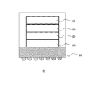
そのため、TSVを有し、低比誘電率膜が用いられた半導体装置の場合、低比誘電率膜にクラックが発生しやすく、発生後の進行も速いという問題がある。図12を参照して具体的に説明する。 Therefore, in the case of a semiconductor device having a TSV and using a low relative dielectric constant film, there is a problem that cracks are likely to occur in the low relative dielectric constant film and the progress after the occurrence is fast. This will be specifically described with reference to FIG.
図12は、他の半導体装置と接続するためのTSVを備え、低比誘電率膜が用いられた半導体装置の一例の断面図を示す。図12に示すように、該半導体装置10は、ウェハの裏面から表面までの順に、シリコン基板20、拡散層LD、コンタクト層LC、第1の銅配線層LCU1、第1のビア層LV1、第2の銅配線層LCU2、第2のビア層LV2、第3の銅配線層LCU3、第3のビア層LV3、第4の銅配線層LCU4、第4のビア層LV4、第5の銅配線層LCU5、アルミ電極30が設けられている。半導体素子の一例として、トランジスタとなる半導体素子40が示されている。
FIG. 12 is a cross-sectional view of an example of a semiconductor device including a TSV for connecting to another semiconductor device and using a low relative dielectric constant film. As shown in FIG. 12, the
ここで第1の銅配線層、第2の銅配線層および第3の銅配線層は、その上層配線と比べて配線ピッチが小さい。配線間の寄生容量を低減するため、第1の銅配線層LCU1と第2の銅配線層LCU2間の絶縁膜51、第2の銅配線層LCU2と第3の銅配線層LCU3間の絶縁膜52、第3の銅配線層LCU3と第4の銅配線層LCU4間の絶縁膜53は、低比誘電率膜が用いられている。なお、斜線で示される絶縁膜54は一般的な酸化珪素が用いられる。
Here, the first copper wiring layer, the second copper wiring layer, and the third copper wiring layer have a smaller wiring pitch than the upper layer wiring. In order to reduce the parasitic capacitance between the wirings, the
また、第1の銅配線層LCU1からシリコン基板20を貫通するTSV60が設けられている。TSV60は、TSV電極61とTSV電極パッド62を含み、TSV電極61が第1の銅配線層LCU1に接続され、TSV電極パッド62がウェハ裏面に設けられており、図示しない他の半導体装置のアルミ電極と接続される。
A TSV 60 penetrating the
半導体装置によって、TSVは、半導体装置の裏面から表面までを貫通する構造や、半導体装置の裏面から半導体装置の第1配線層下まで貫通する構造等、幾つかの構造が開発されている。図12に示す例の半導体装置10では、TSV60は、ウェハ裏面から第1の銅配線層LCU1に接続される部分までを貫通する構造を有する。また、図12の例では、TSV60のTSV電極61は、各層の銅配線及び各層のビアにより、アルミ電極30に接続され、半導体装置10には、他に分岐する銅配線が無い。
Depending on the semiconductor device, several structures have been developed for the TSV, such as a structure penetrating from the back surface to the front surface of the semiconductor device and a structure penetrating from the back surface of the semiconductor device to the first wiring layer of the semiconductor device. In the
熱サイクル試験等、高い温度負荷がかかった場合に、TSV60と、半導体装置10内の半導体素子の熱膨張率の相違に起因して、第1の銅配線層LCU1からアルミ電極30までの、TSV60と接続した部分が、上方に突き上げられたり、下方に引っ張られたりするなどのことが生じる。そのため、この部分の周辺の絶縁膜に熱応力がかかってしまい、クラックの発生が起こり得る。特に、絶縁膜51〜53は、機械的強度が弱い低比誘電率膜であるため、他の絶縁膜(図示せず)より、クラックの発生がしやすい。
When a high temperature load is applied, such as a thermal cycle test, the TSV 60 from the first copper wiring layer LCU1 to the
その他の課題と新規な特徴は、本明細書の記述および添付図面から明らかになるであろう。 Other problems and novel features will become apparent from the description of the specification and the accompanying drawings.
一実施の形態による半導体装置は、シリコン基板を貫通するTSVを備える。シリコン基板に最も近い低比誘電率膜から、シリコン基板から最も遠い低比誘電率膜までシールリングが設けられている。該シールリングは、シリコン基板を俯瞰する方向で見たときに、TSVを囲むように形成されている。 A semiconductor device according to an embodiment includes a TSV penetrating a silicon substrate. A seal ring is provided from the low relative dielectric constant film closest to the silicon substrate to the low relative dielectric constant film farthest from the silicon substrate. The seal ring is formed so as to surround the TSV when the silicon substrate is viewed in an overhead direction.
前記一実施の形態の半導体装置によれば、低比誘電率膜のクラックの発生、またはクラックの進行を抑制することができる。 According to the semiconductor device of the one embodiment, the occurrence of cracks in the low relative dielectric constant film or the progress of cracks can be suppressed.
説明の明確化のため、以下の記載及び図面は、適宜、省略、及び簡略化がなされている。また、各図面において、同一の要素には同一の符号が付されており、必要に応じて重複説明は省略されている。 For clarity of explanation, the following description and drawings are omitted and simplified as appropriate. Moreover, in each drawing, the same code | symbol is attached | subjected to the same element and duplication description is abbreviate | omitted as needed.
<第1の実施の形態>
図1は、第1の実施の形態にかかる3次元集積回路80を示す。3次元集積回路80は、パッケージ基板90の上に、4つの半導体装置100が積層されている。例として、パッケージ基板90の上に積層された半導体装置の数が4であるが、この数は、限定されることがなく、2以上の任意の値とすることができる。
<First Embodiment>
FIG. 1 shows a three-dimensional
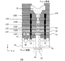
図2は、3次元集積回路80における各半導体装置100の断面図を示す。比較しやすいように、半導体装置100におけるTSVの構造を図12に示す従来の半導体装置10におけるTSVの構造と同様にしている。また、説明上の便宜のため、シリコン基板20からアルミ電極30まで伸びる方向、すなわち半導体装置100の下から上に伸びる方向をY方向とし、Y方向と垂直する方向をX方向とする。
FIG. 2 shows a cross-sectional view of each
図2において、黒く塗りつぶされた部分は、シールリング110を示す。図2から分かるように、該シールリング110は、Y方向に沿って、シリコン基板20に最も近い低比誘電率膜(以下「第1の低比誘電率膜」という)51から、シリコン基板20から最も遠い低比誘電率膜(以下「第2の低比誘電率膜」という)53まで、シールリング110が設けられている。
In FIG. 2, the blackened portion indicates the
図3は、アルミ電極30からシリコン基板20を俯瞰する方向で見たときの、シールリング110の形状と、シールリング110とTSV60の位置関係を示す図である。
FIG. 3 is a diagram illustrating the shape of the
限定されないが、本実施の形態において、シールリング110の形状は、シリコン基板20を俯瞰する方向で見たときに、四方形の4つの角を夫々45度にカットして得た八角形となっている。この形状の意義については、後述する。
Although not limited, in the present embodiment, the shape of the
図3に示すように、シールリング110は、シリコン基板20を俯瞰する方向で見たときに、TSV60(具体的にはTSV電極61)の外周から空隙をおいて、TSV電極61を囲むように、TSV60に近傍に形成されている。
As shown in FIG. 3, the
図4は、図2に示す半導体装置100に生じ得るクラック及びその進行方向の例を示す。半導体装置の各層において、TSVと接続された部分に近い領域ほどクラックが発生しやすい。この例では、丸により囲まれた部分内の低比誘電率膜52の領域にクラックが生じており、図中矢印が示すように、クラックの進行方向は、半導体装置100の外周に向かう方向である。
FIG. 4 shows an example of cracks that can occur in the
図5は、シリコン基板20を俯瞰する方向で見たときの、クラックの進行方向を示す。図5中心部の黒丸は、TSVの中心を示し、各矢印は、クラックの進行方向を示す。
FIG. 5 shows the progressing direction of the cracks when the
クラックは、TSVの中心から放射線状に、半導体装置の外周に向かって進行する。本実施の形態において、シールリング110により、クラックの進行を阻止するため、低比誘電率膜のダメージを小さく抑制することができる。
The cracks progress radially from the center of the TSV toward the outer periphery of the semiconductor device. In this embodiment, since the progress of cracks is prevented by the
また、シールリング110が膜を支持する効用もあるため、シールリング110を設けることにより、クラックの発生そのものも抑制することができる。
Further, since the
次いで、シールリング110の形状の意義を説明する。
例えば、クラックの1つの進行方向が方向1であるとする。方向1に向かって進行するクラックを阻止するためには、方向1と略垂直する形状を有する阻止物が効果的であると考えられる。
Next, the significance of the shape of the
For example, it is assumed that one traveling direction of the crack is the direction 1. In order to prevent cracks proceeding in the direction 1, a blocking object having a shape substantially perpendicular to the direction 1 is considered to be effective.
図5に示すように、クラックは、放射線状に進行する。阻止物となるシールリング110の形状を、四方形の4つの角を夫々45度にカットして得た八角形にすることにより、クラックの各進行方向のうちの、シールリング110と略垂直する方向を増やすことができ、ひいては、クラックの阻止効果を高めることができる。
As shown in FIG. 5, the cracks progress radially. By making the shape of the
<第2の実施の形態>
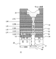
第2の実施の形態も、複数の半導体装置が積層されてなる3次元集積回路である。図6は、本第2の実施の形態にかかる3次元集積回路における半導体装置200を示す。
<Second Embodiment>
The second embodiment is also a three-dimensional integrated circuit in which a plurality of semiconductor devices are stacked. FIG. 6 shows a
半導体装置200は、シールリング110の代わりにシールリング210が設けられた点を除き、半導体装置100と同様である。なお、図6において、シールリング210も、黒く塗りつぶされた部分で示されている。
The
半導体装置100では、シールリング110は、第1の低比誘電率膜51から第2の低比誘電率膜53まで設けられている。対して、図6に示すように、半導体装置200において、シールリング210は、上には、トップの銅配線層(ここでは第5の銅配線層LCU5)まで伸びており、下には、コンタクト層LCまで伸びている。
In the
このように、第1の低比誘電率膜51より下の層から、第2の低比誘電率膜53より上の層までシールリングを設けることにより、低比誘電率膜のみならず、他の層におけるクラックの発生と進行の阻止効果をより高めることができる。
Thus, by providing a seal ring from a layer below the first low relative dielectric
勿論、シールリングは、そのカバー範囲内に、第1の低比誘電率膜51から第2の低比誘電率膜53が含まれていれば、上限については、トップの銅配線層に限らず、半導体装置200の配線状況に応じて、第2の低比誘電率膜53以上の任意の層としてもよい。同様に、下限についても、コンタクト層LCに限らず、半導体装置200の配線状況に応じて、第1の低比誘電率膜51以下の任意の層としてもよい。
Of course, if the first low relative dielectric
<第3の実施の形態>
第3の実施の形態も、複数の半導体装置が積層されてなる3次元集積回路である。図7は、本第3の実施の形態にかかる3次元集積回路における半導体装置300を示す。図7に対して、半導体装置200と異なる点についてのみ説明する。
<Third Embodiment>
The third embodiment is also a three-dimensional integrated circuit in which a plurality of semiconductor devices are stacked. FIG. 7 shows a
半導体装置300は、複数のTSV(図示の例では2つ)を有する。図示のように、TSV60に加え、TSV360が設けられている。TSV360は、TSV電極361とTSV電極パッド362を備え、TSV電極361からアルミ電極330までの接続態様は、TSV60のTSV電極61からアルミ電極30までの接続態様と同様である。
The
また、半導体装置300では、半導体装置200におけるシールリング210の代わりに、シールリング310が設けられている。なお、図7において、シールリング310も、黒く塗りつぶされた部分で示されている。
In the
シールリング310は、Y方向において、シールリング210と同様に、コンタクト層LCから第5の銅配線層LCU5まで設けられている。
Similar to the
図8は、ウェハ表面からシリコン基板20を俯瞰する方向で見たときの、TSV60、TSV360、シールリング310の位置関係を示す図である。
FIG. 8 is a diagram showing the positional relationship between
図示のように、シールリング310は、TSV60(具体的にはTSV電極61)とTSV360(具体的にはTSV電極361)の近傍に、TSV電極61とTSV電極361を囲むように、TSV60とTSV360の近傍に形成されている。その形状は、シールリング110及びシールリング210と同様に、八角形になっている。
As shown in the drawing, the
このように、シリコン基板を俯瞰する方向で見たときに、複数のTSVを囲むようにシールリングを形成することにより、絶縁膜のクラックの発生と進行を抑制することができると共に、TSV毎にシールリングを設けることより、シールリングの本数を減らし、半導体装置のレイアウト上の余裕を大きくすることができる。 As described above, when the silicon substrate is viewed in a bird's-eye view, by forming a seal ring so as to surround a plurality of TSVs, generation and progress of cracks in the insulating film can be suppressed, and for each TSV. By providing the seal ring, the number of seal rings can be reduced and the margin in the layout of the semiconductor device can be increased.
なお、図7は、半導体装置に含まれるTSVの数が2であり、該2つのTSVに対して1本のシールリングを設けた例である。例えば、TSVの数が3以上である場合に、TSV間の間隔や、半導体装置の配線状況などに応じて、これらのTSVを複数のグループに分け、グループ毎にシールリングを設けるようにしてもよい。 FIG. 7 shows an example in which the number of TSVs included in the semiconductor device is 2, and one seal ring is provided for the two TSVs. For example, when the number of TSVs is 3 or more, these TSVs may be divided into a plurality of groups according to the interval between TSVs or the wiring status of the semiconductor device, and a seal ring may be provided for each group. Good.
勿論、シールリング310についても、Y方向において、下限を第1の低比誘電率膜51以下の任意の層、上限を第2の低比誘電率膜53以上の任意の層としてもよい。
Of course, the lower limit of the
<第4の実施の形態>
上述した各実施の形態における半導体装置は、TSVがアルミ電極まで接続された例である。本技術は、TSVがアルミ電極に接続されない半導体装置にも適用可能である。本第4の実施の形態は、このような半導体装置について説明する。
<Fourth embodiment>
The semiconductor device in each embodiment described above is an example in which the TSV is connected to the aluminum electrode. The present technology can also be applied to a semiconductor device in which TSV is not connected to an aluminum electrode. In the fourth embodiment, such a semiconductor device will be described.
図9は、第4の実施の形態にかかる3次元集積回路における半導体装置400を示す。この半導体装置400は、例えば3次元集積回路の最上層の半導体装置である。
FIG. 9 shows a
図9に示すように、半導体装置400において、TSV60は、第5の銅配線層LCU5まで接続されている。また、第5の銅配線層LCU5は、第4のビア層LV4、第3の銅配線層LCU3、第3のビア層LV3、第2の銅配線層LCU2、第2のビア層LV2、第1の銅配線層LCU1、コンタクト層LCを介して、半導体素子40に接続されている。
As shown in FIG. 9, in the
黒く塗りつぶされた部分で示されるシールリング410は、コンタクト層LCから第5の銅配線層LCU5より1つ下の銅配線層(第4の銅配線層LCU4)まで設けられている。
A
こうすることにより、シールリング410は、第5の銅配線層LCU5から半導体素子40までの配線の妨げにはならずに、各低比誘電率膜のクラックの発生と進行を抑制することができる。
By doing so, the
なお、半導体装置400では、シールリング410は、下方向には、コンタクト層LCまで設けられているが、コンタクト層LCに設けずに、第1の低比誘電率膜51まで設けられるようにしてもよい。勿論、上方向においては、第4の銅配線層LCU4に設けずに、第2の低比誘電率膜53まで設けるようにしてもよい。
In the
<第5の実施の形態>
シリコン基板に最も近い低比誘電率膜(第1の低比誘電率膜)から、シリコン基板から最も遠い低比誘電率膜(第2の低比誘電率膜)までシールリングを設ければ、低比誘電率膜のクラックの発生と進行を抑制できることは、上記にて説明した。シールリングを第1の低比誘電率膜より下のコンタクト層まで、すなわち拡散層の表面まで設け、拡散層と接続することにより、シールリングを基板と同電位にすることができる。そのため、近傍の半導体素子への給電に利用することができる。図9を参照して1例を説明する。
<Fifth embodiment>
If a seal ring is provided from the low relative dielectric constant film (first low relative dielectric constant film) closest to the silicon substrate to the low relative dielectric constant film (second low dielectric constant film) farthest from the silicon substrate, As described above, the generation and progress of cracks in the low dielectric constant film can be suppressed. By providing the seal ring up to the contact layer below the first low relative dielectric constant film, that is, up to the surface of the diffusion layer, and connecting to the diffusion layer, the seal ring can have the same potential as the substrate. Therefore, it can be used for power feeding to nearby semiconductor elements. An example will be described with reference to FIG.
図10は、第5の実施の形態にかかる3次元集積回路における半導体装置500の断面図である。図10において、第2の銅配線層LCU2まで示し、第2の銅配線層LCU2より上の層については、図示を省略する。
FIG. 10 is a cross-sectional view of the
半導体装置500において、黒く塗りつぶされた部分で示されるシールリング510は、拡散層LDまで設けられている。
In the
半導体素子40は、例えば、N型のトランジスタであり、拡散層LDは、P+拡散層となる。半導体素子40のドレイン電極とソース電極(GND)は、第1の銅配線層LCU1に設けられており、コンタクト層LCを介して半導体素子40のドレイン端子とソース端子に夫々給電する。
The
この場合、第1の銅配線層LCU1において、接続配線によりシールリング510と半導体素子40のドレイン電極に接続することにより、半導体素子40のソース端子に給電可能である。
In this case, in the first copper wiring layer LCU1, power can be supplied to the source terminal of the
<第6の実施の形態>
図11に示す第6の実施の形態の半導体装置600も、拡散層までシールリングを設け、半導体素子の給電に使用する例である。半導体装置600においても、例として、半導体素子40は、N型のトランジスタであり、拡散層LDは、P+拡散層となる。
<Sixth Embodiment>
The
TSV60は、TSV電極パッド62を介して図示しない外部のGNDに接続されている。この場合、図示のように、第1の銅配線層LCU1において、シールリング610と、半導体素子40のドレイン電極と、TSV60のTSV電極61とを接続配線により接続することにより、半導体素子40のソース端子への給電が可能である。
The
以上、本発明者によってなされた発明を実施の形態に基づき具体的に説明したが、本発明は既に述べた実施の形態に限定されるものではなく、その要旨を逸脱しない範囲において種々の変更が可能であることはいうまでもない。 As mentioned above, the invention made by the present inventor has been specifically described based on the embodiments. However, the present invention is not limited to the embodiments already described, and various modifications can be made without departing from the scope of the invention. It goes without saying that it is possible.
10 半導体装置
20 シリコン基板
30 アルミ電極
40 半導体素子
51 第1の低比誘電率膜
52 低比誘電率膜
53 第2の低比誘電率膜
54 絶縁膜
60 TSV
61 TSV電極
62 TSV電極パッド
80 3次元集積回路
90 パッケージ基板
100 半導体装置
110 シールリング
200 半導体装置
210 シールリング
300 半導体装置
310 シールリング
330 アルミ電極
360 TSV
361 TSV電極
362 TSV電極パッド
400 半導体装置
410 シールリング
500 半導体装置
510 シールリング
600 半導体装置
610 シールリング
LC コンタクト層
LD 拡散層
LCU1 第1の銅配線層
LCU2 第2の銅配線層
LCU3 第3の銅配線層
LCU4 第4の銅配線層
LCU5 第5の銅配線層
LV1 第1のビア層
LV2 第2のビア層
LV3 第3のビア層
LV4 第4のビア層
DESCRIPTION OF
61
361
Claims (4)
前記シリコン基板を貫通するTSV(Through−Silicon Via)とを備える半導体装置であって、
前記シリコン基板に最も近い低比誘電率膜である第1の低比誘電率膜から、前記シリコン基板から最も遠い低比誘電率膜である第2の低比誘電率膜までシールリングが設けられており、
前記シールリングは、前記シリコン基板を俯瞰する方向で見たときに、前記TSVの近傍において前記TSVを囲むように形成されており、
前記シールリングは、前記第1の低比誘電率膜より下のコンタクト層まで設けられ、拡散層に接続されており、
前記シールリングは、半導体素子の電極にさらに接続されており、
前記拡散層から前記シールリングを介して前記半導体素子の電極に対して給電される、
半導体装置。 A silicon substrate;
A semiconductor device comprising a TSV (Through-Silicon Via) penetrating the silicon substrate,
A seal ring is provided from the first low relative dielectric constant film, which is the low relative dielectric constant film closest to the silicon substrate, to the second low relative dielectric constant film, which is the low relative dielectric constant film farthest from the silicon substrate. And
The seal ring is formed so as to surround the TSV in the vicinity of the TSV when viewed in a direction in which the silicon substrate is viewed from above .
The seal ring is provided up to a contact layer below the first low dielectric constant film, and is connected to a diffusion layer,
The seal ring is further connected to an electrode of the semiconductor element;
Power is supplied from the diffusion layer to the electrode of the semiconductor element through the seal ring.
Semiconductor device.
請求項1に記載の半導体装置。 The seal ring is provided up to a layer above the second low dielectric constant film,
The semiconductor device according to claim 1 .
前記シールリングは、前記シリコン基板を俯瞰する方向で見たときに、前記複数のTSVを囲むように形成されている、
請求項1又は2に記載の半導体装置。 A plurality of the TSVs;
The seal ring is formed so as to surround the plurality of TSVs when viewed in a direction of overlooking the silicon substrate.
The semiconductor device according to claim 1 or 2.
前記シリコン基板を俯瞰する方向で見たときに、四方形の4つの角を夫々45度にカットして得た八角形を成す、
請求項1から3のいずれか1項に記載の半導体装置。 The seal ring is
When the silicon substrate is viewed in a bird's-eye view, it forms an octagon obtained by cutting four corners of a quadrangle at 45 degrees,
The semiconductor device according to any one of claims 1 to 3.
Priority Applications (4)
| Application Number | Priority Date | Filing Date | Title |
|---|---|---|---|
| JP2012272137A JP6157100B2 (en) | 2012-12-13 | 2012-12-13 | Semiconductor device |
| US14/077,503 US9673153B2 (en) | 2012-12-13 | 2013-11-12 | Semiconductor device |
| CN201310685194.9A CN103872047B (en) | 2012-12-13 | 2013-12-13 | Semiconductor devices |
| US15/585,468 US10062655B2 (en) | 2012-12-13 | 2017-05-03 | Semiconductor device |
Applications Claiming Priority (1)
| Application Number | Priority Date | Filing Date | Title |
|---|---|---|---|
| JP2012272137A JP6157100B2 (en) | 2012-12-13 | 2012-12-13 | Semiconductor device |
Related Child Applications (1)
| Application Number | Title | Priority Date | Filing Date |
|---|---|---|---|
| JP2017111407A Division JP2017147475A (en) | 2017-06-06 | 2017-06-06 | Semiconductor device |
Publications (3)
| Publication Number | Publication Date |
|---|---|
| JP2014120504A JP2014120504A (en) | 2014-06-30 |
| JP2014120504A5 JP2014120504A5 (en) | 2015-10-08 |
| JP6157100B2 true JP6157100B2 (en) | 2017-07-05 |
Family
ID=50910421
Family Applications (1)
| Application Number | Title | Priority Date | Filing Date |
|---|---|---|---|
| JP2012272137A Active JP6157100B2 (en) | 2012-12-13 | 2012-12-13 | Semiconductor device |
Country Status (3)
| Country | Link |
|---|---|
| US (2) | US9673153B2 (en) |
| JP (1) | JP6157100B2 (en) |
| CN (1) | CN103872047B (en) |
Families Citing this family (6)
| Publication number | Priority date | Publication date | Assignee | Title |
|---|---|---|---|---|
| CN105336710B (en) * | 2014-07-10 | 2018-03-23 | 中芯国际集成电路制造(上海)有限公司 | A kind of sealing ring of chip |
| JP6519785B2 (en) * | 2015-05-11 | 2019-05-29 | 国立研究開発法人産業技術総合研究所 | Through electrode, method of manufacturing the same, semiconductor device, and method of manufacturing the same |
| JP6713481B2 (en) | 2015-10-28 | 2020-06-24 | オリンパス株式会社 | Semiconductor device |
| CN108155155B (en) * | 2016-12-02 | 2020-03-10 | 中芯国际集成电路制造(上海)有限公司 | Semiconductor structure and forming method thereof |
| CN109830464A (en) * | 2019-02-15 | 2019-05-31 | 德淮半导体有限公司 | Semiconductor structure and forming method thereof |
| US20230187289A1 (en) * | 2021-12-14 | 2023-06-15 | Micron Technology, Inc. | Semiconductor device and method of forming the same |
Family Cites Families (22)
| Publication number | Priority date | Publication date | Assignee | Title |
|---|---|---|---|---|
| JP4502173B2 (en) * | 2003-02-03 | 2010-07-14 | ルネサスエレクトロニクス株式会社 | Semiconductor device and manufacturing method thereof |
| US7049701B2 (en) * | 2003-10-15 | 2006-05-23 | Kabushiki Kaisha Toshiba | Semiconductor device using insulating film of low dielectric constant as interlayer insulating film |
| JP2005142553A (en) * | 2003-10-15 | 2005-06-02 | Toshiba Corp | Semiconductor device |
| JP4689244B2 (en) * | 2004-11-16 | 2011-05-25 | ルネサスエレクトロニクス株式会社 | Semiconductor device |
| US7224069B2 (en) * | 2005-07-25 | 2007-05-29 | Taiwan Semiconductor Manufacturing Company, Ltd. | Dummy structures extending from seal ring into active circuit area of integrated circuit chip |
| JP5021992B2 (en) * | 2005-09-29 | 2012-09-12 | ルネサスエレクトロニクス株式会社 | Semiconductor device and manufacturing method thereof |
| JP2007115988A (en) * | 2005-10-21 | 2007-05-10 | Renesas Technology Corp | Semiconductor device |
| JP5098647B2 (en) * | 2005-12-27 | 2012-12-12 | 富士通セミコンダクター株式会社 | Semiconductor device and manufacturing method thereof |
| JP5329068B2 (en) | 2007-10-22 | 2013-10-30 | ルネサスエレクトロニクス株式会社 | Semiconductor device |
| JP2009123734A (en) * | 2007-11-12 | 2009-06-04 | Renesas Technology Corp | Semiconductor device, and manufacturing method thereof |
| US8188578B2 (en) * | 2008-05-29 | 2012-05-29 | Mediatek Inc. | Seal ring structure for integrated circuits |
| US8053902B2 (en) | 2008-12-02 | 2011-11-08 | Taiwan Semiconductor Manufacturing Company, Ltd. | Isolation structure for protecting dielectric layers from degradation |
| US8749027B2 (en) * | 2009-01-07 | 2014-06-10 | Taiwan Semiconductor Manufacturing Company, Ltd. | Robust TSV structure |
| US8299583B2 (en) * | 2009-03-05 | 2012-10-30 | International Business Machines Corporation | Two-sided semiconductor structure |
| US20100224878A1 (en) | 2009-03-05 | 2010-09-09 | Semiconductor Energy Laboratory Co., Ltd. | Semiconductor device |
| US8169055B2 (en) | 2009-03-18 | 2012-05-01 | International Business Machines Corporation | Chip guard ring including a through-substrate via |
| JP2011129722A (en) | 2009-12-17 | 2011-06-30 | Panasonic Corp | Semiconductor device |
| JP2011176047A (en) * | 2010-02-23 | 2011-09-08 | On Semiconductor Trading Ltd | Semiconductor device and method of manufacturing the same |
| JP2011216753A (en) | 2010-04-01 | 2011-10-27 | Panasonic Corp | Semiconductor device, and method of manufacturing the same |
| JP5300814B2 (en) | 2010-10-14 | 2013-09-25 | ルネサスエレクトロニクス株式会社 | Semiconductor device |
| JP5685060B2 (en) * | 2010-11-18 | 2015-03-18 | ルネサスエレクトロニクス株式会社 | Semiconductor device |
| JP2012256787A (en) * | 2011-06-10 | 2012-12-27 | Renesas Electronics Corp | Semiconductor device and semiconductor device manufacturing method |
-
2012
- 2012-12-13 JP JP2012272137A patent/JP6157100B2/en active Active
-
2013
- 2013-11-12 US US14/077,503 patent/US9673153B2/en not_active Expired - Fee Related
- 2013-12-13 CN CN201310685194.9A patent/CN103872047B/en not_active Expired - Fee Related
-
2017
- 2017-05-03 US US15/585,468 patent/US10062655B2/en active Active
Also Published As
| Publication number | Publication date |
|---|---|
| JP2014120504A (en) | 2014-06-30 |
| US20140167286A1 (en) | 2014-06-19 |
| US9673153B2 (en) | 2017-06-06 |
| CN103872047A (en) | 2014-06-18 |
| US20170236789A1 (en) | 2017-08-17 |
| CN103872047B (en) | 2018-02-27 |
| US10062655B2 (en) | 2018-08-28 |
Similar Documents
| Publication | Publication Date | Title |
|---|---|---|
| JP6157100B2 (en) | Semiconductor device | |
| KR101227872B1 (en) | Esd protection structure for 3d ic | |
| CN103378034B (en) | There is the semiconductor packages of silicon through hole intraconnections | |
| US9087822B2 (en) | Semiconductor device | |
| JP2007184449A (en) | Semiconductor device and its manufacturing method | |
| US9947627B2 (en) | Guard ring structure and method for forming the same | |
| EP2733736A2 (en) | Method for electrically connecting wafers using butting contact struture and semiconductor device fabricated through the same | |
| TWI596737B (en) | Electrostatic discharge protection device | |
| CN103579208A (en) | Three-dimensional integrated circuits and fabrication thereof | |
| US20160172406A1 (en) | Semiconductor device and solid-state imaging device | |
| TW201801263A (en) | Fan-out wafer level package structure | |
| TWI520330B (en) | Semiconductor device | |
| JP5359072B2 (en) | Semiconductor device | |
| US11450633B2 (en) | Package structure of semiconductor device with improved bonding between the substrates | |
| TWI529872B (en) | Radio-frequency device package and method for fabricating the same | |
| JP2017147475A (en) | Semiconductor device | |
| US8350272B2 (en) | Semiconductor device | |
| JP5574639B2 (en) | Semiconductor device and manufacturing method thereof | |
| US9269645B1 (en) | Fan-out wafer level package | |
| JP2014022485A (en) | Semiconductor device and manufacturing method of the same | |
| JP2011066459A (en) | Semiconductor device | |
| JP5401056B2 (en) | Semiconductor device | |
| JP2014192295A (en) | Semiconductor device | |
| JP6211855B2 (en) | Semiconductor device | |
| JP5920239B2 (en) | Semiconductor device |
Legal Events
| Date | Code | Title | Description |
|---|---|---|---|
| A521 | Request for written amendment filed |
Free format text: JAPANESE INTERMEDIATE CODE: A523 Effective date: 20150820 |
|
| A621 | Written request for application examination |
Free format text: JAPANESE INTERMEDIATE CODE: A621 Effective date: 20150820 |
|
| A977 | Report on retrieval |
Free format text: JAPANESE INTERMEDIATE CODE: A971007 Effective date: 20160720 |
|
| A131 | Notification of reasons for refusal |
Free format text: JAPANESE INTERMEDIATE CODE: A131 Effective date: 20160906 |
|
| A521 | Request for written amendment filed |
Free format text: JAPANESE INTERMEDIATE CODE: A523 Effective date: 20161102 |
|
| TRDD | Decision of grant or rejection written | ||
| A01 | Written decision to grant a patent or to grant a registration (utility model) |
Free format text: JAPANESE INTERMEDIATE CODE: A01 Effective date: 20170509 |
|
| A61 | First payment of annual fees (during grant procedure) |
Free format text: JAPANESE INTERMEDIATE CODE: A61 Effective date: 20170606 |
|
| R150 | Certificate of patent or registration of utility model |
Ref document number: 6157100 Country of ref document: JP Free format text: JAPANESE INTERMEDIATE CODE: R150 |