JP6155733B2 - Liquid ejection device and capacitive load drive circuit - Google Patents
Liquid ejection device and capacitive load drive circuit Download PDFInfo
- Publication number
- JP6155733B2 JP6155733B2 JP2013059209A JP2013059209A JP6155733B2 JP 6155733 B2 JP6155733 B2 JP 6155733B2 JP 2013059209 A JP2013059209 A JP 2013059209A JP 2013059209 A JP2013059209 A JP 2013059209A JP 6155733 B2 JP6155733 B2 JP 6155733B2
- Authority
- JP
- Japan
- Prior art keywords
- voltage
- piezoelectric element
- signal path
- control signal
- state
- Prior art date
- Legal status (The legal status is an assumption and is not a legal conclusion. Google has not performed a legal analysis and makes no representation as to the accuracy of the status listed.)
- Expired - Fee Related
Links
Images


Landscapes
- Particle Formation And Scattering Control In Inkjet Printers (AREA)
Description
本発明は、液体吐出装置および容量性負荷回路に関する。 The present invention relates to a liquid ejection device and a capacitive load circuit.
インクを吐出して画像や文書を印刷するインクジェットプリンターには、圧電素子(例えばピエゾ素子)を用いたものが知られている。圧電素子は、印刷ヘッドにおける複数のノズルのそれぞれに対応して設けられる。詳細には、圧電素子は、ノズルに連通するとともに流路を介してインクが供給されるキャビティ(インク室)に設けられ、圧電素子に印加される制御信号の電圧変化によって、キャビティの容積を変位させる。ここで、制御信号の電圧が上昇すれば、キャビティの容積が拡大してインクが引き込まれる一方、制御信号の電圧が下降すれば、キャビティの容積が縮小してインクが吐出される構成となっている(例えば特許文献1参照)。 2. Related Art An ink jet printer that prints an image or a document by ejecting ink is known that uses a piezoelectric element (for example, a piezo element). The piezoelectric element is provided corresponding to each of the plurality of nozzles in the print head. Specifically, the piezoelectric element communicates with the nozzle and is provided in a cavity (ink chamber) to which ink is supplied via a flow path, and the volume of the cavity is displaced by a voltage change of a control signal applied to the piezoelectric element. Let Here, if the voltage of the control signal increases, the volume of the cavity expands and ink is drawn, while if the voltage of the control signal decreases, the volume of the cavity decreases and ink is ejected. (For example, refer to Patent Document 1).
圧電素子は、電気的にみればキャパシターのような容量性負荷であるので、各ノズルの圧電素子を動作させるためには十分な電流を供給する必要がある。このため、原信号を増幅回路で増幅し、増幅された制御信号を印刷ヘッドに供給して、圧電素子を駆動する構成が一般的であったが、装置の省電力化を図る必要性などの理由により、圧電素子に電圧を複数段階で切り替えて供給する方式(電圧切替方式、特許文献2参照)が提案されている。 Since the piezoelectric element is a capacitive load such as a capacitor when viewed electrically, it is necessary to supply a sufficient current to operate the piezoelectric element of each nozzle. For this reason, a configuration in which the original signal is amplified by an amplifier circuit, the amplified control signal is supplied to the print head, and the piezoelectric element is driven is generally used. For this reason, there has been proposed a method of switching and supplying a voltage to a piezoelectric element in a plurality of stages (voltage switching method, see Patent Document 2).
ところで、上記電圧切替方式では、圧電素子に印加する電圧を、ある値から別の値に変化させるときに、圧電素子に印加される電圧波形が階段状の段差を伴ってしまう箇所がある。
インクを吐出するために制御信号の電圧を直線的に低下させるときに、圧電素子に印加される電圧が階段状になってしまうと、キャビティからインクが段階的に突出されてしまう、端的にいえば、インクが予期せずに複数滴になって吐出されてしまうことがある。インクが複数滴になって吐出されると、ミスト(霧)となって装置内部の各所に付着し、汚れや故障の原因となるだけでなく、紙などの被記録材に着弾しないので、画質を劣化させる、という問題がある。
そこで、本発明のいくつかの態様の目的の一つは、省電力化を図るとともに、ある電圧から別の電圧に直線的に変化させる際に、圧電素子に印加される電圧が階段状にならないように制御して、インクが複数滴になってしまうことを防止した液体吐出装置および容量性負荷駆動回路を提供することにある。
By the way, in the voltage switching method, when the voltage applied to the piezoelectric element is changed from a certain value to another value, there is a portion where the voltage waveform applied to the piezoelectric element is accompanied by a stepped step.
When the voltage of the control signal is lowered linearly to eject ink, if the voltage applied to the piezoelectric element becomes stepped, the ink will protrude stepwise from the cavity. In this case, the ink may be ejected as a plurality of droplets unexpectedly. When ink is ejected in multiple droplets, it becomes mist (fog) and adheres to various places inside the device, causing not only dirt and failure but also landing on recording materials such as paper. There is a problem of degrading.
Accordingly, one of the objects of some aspects of the present invention is to save power and to make the voltage applied to the piezoelectric element not stepped when changing from one voltage to another linearly. It is an object of the present invention to provide a liquid ejection apparatus and a capacitive load drive circuit that are controlled in such a manner as to prevent ink from becoming a plurality of droplets.
上記目的の一つを達成するために、本発明の一態様に係る液体吐出装置は、液体を吐出するノズルと、前記ノズルに連通する圧力室と、前記圧力室毎に設けられる圧電素子と、を含む吐出部と、電荷を供給する一方で電荷を回収する補助電源と、前記第0電圧の第0信号経路と、前記第0電圧よりも高い第1電圧が前記補助電源によって印加された第1信号経路と、前記第1電圧よりも高い第2電圧の第2信号経路と、制御信号の電圧と前記圧電素子の保持電圧とに応じて、前記圧電素子と前記補助電源との間を、前記第0信号経路、第1信号経路および前記第2信号経路を用いて電気的に接続する接続経路選択部と、を具備し、前記接続経路選択部は、前記圧電素子の保持電圧が前記第1電圧を跨いで低下するとき、前記圧電素子と前記補助電源との間を、前記第1信号経路および前記第0信号経路を介して電気的に接続した状態の後、前記第1信号経路を電気的に非接続にするとともに前記第0信号経路を介して電気的に接続した状態に遷移させることを特徴とする。 In order to achieve one of the above objects, a liquid ejection apparatus according to an aspect of the present invention includes a nozzle that ejects liquid, a pressure chamber that communicates with the nozzle, and a piezoelectric element that is provided for each pressure chamber, An auxiliary power source that supplies charges while collecting charges, a zeroth signal path of the zeroth voltage, and a first voltage that is higher than the zeroth voltage is applied by the auxiliary power supply. 1 signal path, a second signal path of a second voltage higher than the first voltage, a voltage of a control signal and a holding voltage of the piezoelectric element, between the piezoelectric element and the auxiliary power source, A connection path selection unit electrically connected using the 0th signal path, the first signal path, and the second signal path, wherein the connection path selection unit has a holding voltage of the piezoelectric element as the first voltage path. When the voltage drops across one voltage, the piezoelectric element and the complement After the state of being electrically connected to the power source via the first signal path and the zeroth signal path, the first signal path is electrically disconnected and the zeroth signal path is used. And transition to an electrically connected state.
上記一態様に係る液体吐出装置によれば、圧電素子の充電および放電については、基本的には電圧の切り替えで進行するので、電源電圧間で一気に行う従来構成と比較して、エネルギー効率が高くなり、省電力化を図ることができる。くわえて、放電によって圧電素子の保持電圧が第1電圧を跨いで低下するときに、第0信号経路および第1信号経路の双方が接続された状態を経て、第0信号経路のみが接続された状態に遷移する。このため、上記一態様によれば、圧電素子の保持電圧が第1電圧を跨いで低下するときに、第1信号経路のみが接続された状態を経て、第0信号経路のみが接続された状態を経る構成と比較して第1電圧近傍での段差を抑えることができる。 According to the liquid ejection device according to the aspect described above, the charging and discharging of the piezoelectric element basically proceeds by switching the voltage, so that the energy efficiency is higher than that of the conventional configuration that is performed at a time between the power supply voltages. Thus, power saving can be achieved. In addition, when the holding voltage of the piezoelectric element decreases across the first voltage due to discharge, only the 0th signal path is connected through the state where both the 0th signal path and the 1st signal path are connected. Transition to the state. For this reason, according to the above aspect, when the holding voltage of the piezoelectric element decreases across the first voltage, only the first signal path is connected after the first signal path is connected. Compared to the configuration through the first step, the step near the first voltage can be suppressed.
上記態様に係る液体吐出装置において、前記圧電素子の保持電圧が、前記第1電圧よりも予め定められた値だけ高い第1低側閾値電圧未満であるか否か、または、前記第1電圧よりも予め定められた値だけ低い第1高側閾値電圧以上であるか否か、を検出する検出部を有する構成としても良い。この構成によれば、検出部によって圧電素子の保持電圧が、第1高側閾値電圧未満であるか否か、または、第1下側閾値電圧以上であるか否か、すなわち、第1電圧を跨ぐ蓋然性が高いか否かが検出される。なお、検出部としては、圧電素子の保持電圧が第1高側閾値電圧未満であるか否かを検出する部分と、第1下側閾値電圧以上であるか否かを検出する部分とを個別に分けても良いし、一体としても良い。 In the liquid ejection apparatus according to the above aspect, whether or not the holding voltage of the piezoelectric element is less than a first low-side threshold voltage that is higher than the first voltage by a predetermined value, or from the first voltage. Also, it may be configured to include a detection unit that detects whether or not the voltage is equal to or higher than a first high-side threshold voltage that is lower by a predetermined value. According to this configuration, the detection unit determines whether the holding voltage of the piezoelectric element is less than the first high-side threshold voltage, or whether it is greater than or equal to the first lower-side threshold voltage, that is, the first voltage is It is detected whether the probability of straddling is high. As the detection unit, a part for detecting whether or not the holding voltage of the piezoelectric element is less than the first high threshold voltage and a part for detecting whether or not it is equal to or higher than the first lower threshold voltage are individually provided. It may be divided into two types or may be integrated.
上記態様に係る液体吐出装置において、前記接続経路選択部は、前記圧電素子の保持電圧が前記第1低側閾値電圧以上であって前記第1高側閾値電圧未満であるときに、前記圧電素子から前記第0信号経路および前記第1信号経路に放電される電荷を、前記制御信号の電圧に応じて制御し、前記圧電素子の保持電圧が前記第1低側閾値電圧未満であるときに、前記圧電素子から前記第0信号経路に放電される電荷を、前記制御信号の電圧に応じて制御する構成としても良い。この構成によれば、制御信号の電圧にしたがって、圧電素子に放電される電荷が制御される。 In the liquid ejection apparatus according to the aspect, the connection path selection unit may be configured such that when the holding voltage of the piezoelectric element is equal to or higher than the first low-side threshold voltage and lower than the first high-side threshold voltage, the piezoelectric element The electric charge discharged from the first signal path to the first signal path is controlled according to the voltage of the control signal, and when the holding voltage of the piezoelectric element is less than the first low-side threshold voltage, It is good also as a structure which controls the electric charge discharged to the said 0th signal path | route from the said piezoelectric element according to the voltage of the said control signal. According to this configuration, the electric charge discharged to the piezoelectric element is controlled according to the voltage of the control signal.
上記態様に係る液体吐出装置において、前記接続経路選択部は、トランジスターAおよびトランジスターBを含み、前記圧電素子の保持電圧が前記第1低側閾値電圧以上であって前記第1高側閾値電圧未満であるときに、前記トランジスターAは、前記圧電素子から前記第0信号経路に放電される電荷を前記制御信号の電圧に応じて制御し、前記トランジスターBは、前記圧電素子から前記第1信号経路に放電される電荷を前記制御信号の電圧に応じて制御し、前記圧電素子の保持電圧が前記第1低側閾値電圧未満であるときに、前記トランジスターAは、前記圧電素子から前記第0信号経路に放電される電荷を前記制御信号の電圧に応じて制御する構成としても良い。
なお、上記態様において、所定値としては、トランジスターAおよびトランジスターB例えばバイポーラトランジスターであれば、バイアス電圧に相当する電圧とし、例えばMOSFET(Metal-Oxide-Semiconductor Field-Effect Transistor:電界効果トランジスター)であれば、しきい値電圧に相当する電圧とするのが好ましい。
In the liquid ejection apparatus according to the above aspect, the connection path selection unit includes a transistor A and a transistor B, and the holding voltage of the piezoelectric element is equal to or higher than the first low-side threshold voltage and lower than the first high-side threshold voltage. The transistor A controls the charge discharged from the piezoelectric element to the zeroth signal path according to the voltage of the control signal, and the transistor B controls the first signal path from the piezoelectric element. The transistor A is controlled by the piezoelectric element from the piezoelectric element when the holding voltage of the piezoelectric element is lower than the first low-side threshold voltage. It is good also as a structure which controls the electric charge discharged to a path | route according to the voltage of the said control signal.
In the above embodiment, the predetermined value may be a voltage corresponding to the bias voltage in the case of the transistor A and the transistor B, for example, a bipolar transistor, for example, a MOSFET (Metal-Oxide-Semiconductor Field-Effect Transistor). For example, a voltage corresponding to the threshold voltage is preferable.
上記目的の一つを達成するために、本発明の別態様に係る容量性負荷駆動回路は、容量性負荷に充電と放電とを繰り返させる容量性負荷駆動回路であって、電荷を供給する一方で電荷を回収する補助電源と、前記第0電圧の第0信号経路と、前記第0電圧よりも高い第1電圧が前記補助電源によって印加された第1信号経路と、前記第1電圧よりも高い第2電圧の第2信号経路と、制御信号の電圧と前記容量性負荷の保持電圧とに応じて、前記容量性負荷と前記補助電源との間を、前記第0信号経路、第1信号経路および前記第2信号経路を用いて電気的に接続する接続経路選択部と、を具備し、前記接続経路選択部は、前記容量性負荷の保持電圧が前記第1電圧を跨いで低下するとき、前記容量性負荷と前記補助電源との間を、前記第1信号経路および前記第0信号経路を介して電気的に接続した状態の後、前記第1信号経路を電気的に非接続にするとともに前記第0信号経路を介して電気的に接続した状態に遷移させることを特徴とする。
上記別態様に係る容量性負荷駆動回路によれば、容量性負荷の充電および放電については、基本的には電圧の切り替えで進行するので、電源電圧間で一気に行う従来構成と比較して、エネルギー効率が高くなり、省電力化を図ることができる。くわえて、放電によって圧電素子の保持電圧が第1電圧を跨いで低下するときに、第0信号経路および第1信号経路の双方が接続された状態を経て、第0信号経路のみが接続された状態に遷移する。
このため、上記別態様によれば、容量性負荷の保持電圧が第1電圧を跨いで低下するときに、第1信号経路のみが接続された状態を経て、第0信号経路のみが接続された状態を経る構成と比較して第1電圧近傍での段差を抑えることができる。
In order to achieve one of the above objects, a capacitive load driving circuit according to another aspect of the present invention is a capacitive load driving circuit that repeats charging and discharging of a capacitive load, while supplying electric charge. An auxiliary power source for recovering the electric charge, a zeroth signal path of the zeroth voltage, a first signal path to which a first voltage higher than the zeroth voltage is applied by the auxiliary power supply, and a higher voltage than the first voltage. Depending on the second signal path of the high second voltage, the voltage of the control signal and the holding voltage of the capacitive load, the 0th signal path, the first signal between the capacitive load and the auxiliary power supply And a connection path selection unit that is electrically connected using the second signal path, and the connection path selection unit is configured to reduce a holding voltage of the capacitive load across the first voltage. , The first signal between the capacitive load and the auxiliary power source. After the state of being electrically connected via the path and the 0th signal path, the first signal path is electrically disconnected and transitioned to the state of being electrically connected via the 0th signal path It is characterized by that.
According to the capacitive load driving circuit according to the other aspect, the charging and discharging of the capacitive load basically proceeds by switching the voltage. Efficiency increases and power saving can be achieved. In addition, when the holding voltage of the piezoelectric element decreases across the first voltage due to discharge, only the 0th signal path is connected through the state where both the 0th signal path and the 1st signal path are connected. Transition to the state.
For this reason, according to the other aspect, when the holding voltage of the capacitive load decreases across the first voltage, only the first signal path is connected through the state where only the first signal path is connected. A step near the first voltage can be suppressed as compared with the configuration through the state.
以下、図面を参照して本発明を実施するための形態について説明する。 Hereinafter, embodiments for carrying out the present invention will be described with reference to the drawings.
<印刷装置の全体構成>
本発明の実施形態に係る印刷装置は、ホストコンピューターから供給された画像データに応じてインクを吐出することによって紙などの被記録材にインクドット群を形成し、これにより、当該画像データに応じた画像(文字、図形等を含む)を印刷するインクジェットプリンター、すなわち液体吐出装置である。
<Overall configuration of printing apparatus>
A printing apparatus according to an embodiment of the present invention forms ink dot groups on a recording material such as paper by ejecting ink according to image data supplied from a host computer, and thereby according to the image data. Inkjet printers that print images (including characters, graphics, etc.), that is, liquid ejection devices.
図1は、印刷装置1の概略構成を示す図である。
この図に示されるように、印刷装置1は、ホストコンピューターから供給された画像データに基づいて画像の印刷のための演算処理を実行する制御ユニット10と、複数のノズルを有する印刷ヘッド20とを含んだ構成となっている。なお、制御ユニット10と印刷ヘッド20とは、フレキシブルケーブル190を介して電気的に接続される。また、印刷ヘッド20は、被記録材の送り方向(副走査方向)に対してほぼ直交する方向(主走査方向)に移動可能なキャリッジ(図示省略)に搭載される。
FIG. 1 is a diagram illustrating a schematic configuration of the
As shown in this figure, the
制御ユニット10は、主制御部120と、DAC(Digital to Analog Converter)160と、主電源回路180とを含む。
主制御部120は、ホストコンピューターから取得した画像データに基づいて、画像展開処理や、色変換処理、インク色分版処理、ハーフトーン処理などの印刷のための演算処理を実行して、印刷ヘッド20のノズルからインクを吐出させるための複数種類の信号を生成する。複数種類の信号には、DAC160に供給されるデジタルの制御データdCOMや、後述するヘッド制御部220に供給される各種信号が含まれる。
なお、主制御部120が実行する印刷のための各演算処理の内容は、印刷装置の技術分野において周知の事項であるため、説明を省略する。また、印刷装置1としては、印刷ヘッド20を搭載したキャリッジを主走査方向に移動させるキャリッジモーターや、被記録材を副走査方向に搬送するための搬送モーターなどを含み、また、制御ユニット10としては、これらのモーターに駆動信号を供給する構成を含むが、同様に周知の事項であるため、説明を省略する。
The
Based on the image data acquired from the host computer, the main control unit 120 executes arithmetic processing for printing such as image development processing, color conversion processing, ink color separation processing, and halftone processing, and the print head A plurality of types of signals for ejecting ink from the 20 nozzles are generated. The plural types of signals include digital control data dCOM supplied to the
Note that the contents of each arithmetic processing for printing executed by the main control unit 120 are well-known matters in the technical field of the printing apparatus, and thus description thereof is omitted. The
DAC160は、制御データdCOMをアナログの駆動信号COMに変換して印刷ヘッド20に供給する。
主電源回路180は、制御ユニット10の各部や印刷ヘッド20に電源電圧を供給し、特に印刷ヘッド20に対して電源電圧としてVH、Gを供給する。
なお、G(グランド)は接地電位であり、この説明において特に説明のない限り、電圧ゼロの基準としている。また、電圧VHは、実施形態においてグランドGに対し高位側としている。
The
The main
Note that G (ground) is a ground potential, and unless otherwise specified in this description, is a reference of zero voltage. In addition, the voltage V H is on the higher side with respect to the ground G in the embodiment.
印刷ヘッド20には、特に図示しないが、1色または複数色のインクがインク容器から流路を介して供給される。印刷ヘッド20は、補助電源回路50、ヘッド制御部220および選択部230のほか、ドライバー30と圧電素子(ピエゾ素子)40との複数組を含む。
ヘッド制御部220は、主制御部120から供給された各種信号にしたがって選択部230の選択を制御するものである。
Although not specifically shown, the
The
選択部230は、ドライバー30および圧電素子40の複数組のそれぞれに対応したスイッチ232を有し、各スイッチ232の一端は互いに接続されて、制御信号COMが共通に供給される一方、他端は、それぞれに対応するドライバー30の入力端に接続される。各スイッチ232は、ヘッド制御部220による制御にしたがってオン/オフするとともに、オンしたときに制御信号COMをドライバー30に供給する一方、オフしたときに制御信号COMを遮断する。このため、選択部230は、制御ユニット10から供給される制御信号COMをヘッド制御部220にしたがって選択してドライバー30に供給することになる。説明の便宜上、制御信号COMのうち、ヘッド制御部220にしたがって選択されてドライバー30に供給される制御信号をVinと表記する。
The
ドライバー30は、補助電源回路50から供給される複数の電圧と、電源電圧VH、Gとを用いて、選択部230から供給される制御信号Vinにしたがって圧電素子40を駆動する。
圧電素子40の一端は、対応するドライバー30の出力端に接続される一方、圧電素子40の他端はグランドGに共通接地されている。このため、圧電素子40に保持される電圧は、ドライバー30の出力電圧の意味を兼ねるので、電圧Voutと表記している。
補助電源回路50は、具体的な構成については後述するが、主電源回路180から供給される電源電圧VH、Gをチャージポンプ回路によって分圧・再配分することによって、電圧VH/6、2VH/6、3VH/6、4VH/6および5VH/6を生成して、複数のドライバー30にわたって共通に供給する。
The
One end of the
Although the specific configuration of the auxiliary
上述したように圧電素子40は、印刷ヘッド20における複数のノズルのそれぞれに対応して設けられて、その駆動によってインクを吐出させる。そこで次に、圧電素子40への駆動によってインクを吐出させるための構成について簡単に説明する。
As described above, the
図2は、印刷ヘッド20において、ノズル1個分に対応した吐出部400の概略構成を示す図である。
図に示されるように吐出部400は、圧電素子40と振動板421とキャビティ(圧力室)431とリザーバー441とノズル451とを含む。このうち、振動板421は、図において上面に設けられた圧電素子40によって変形して、インクが充填されるキャビティ431の内部容積を拡大/縮小させる。ノズル451は、キャビティ431に連通する開口部である。
FIG. 2 is a diagram illustrating a schematic configuration of the
As shown in the figure, the
この図で示される圧電素子40は、一般にユニモルフ(モノモルフ)型と呼ばれ、圧電体401を一対の電極411、412で挟んだ構造である。この構造の圧電体401にあっては、電極411、412の間に印加された電圧に応じて、電極411、412、振動板421とともに図において中央部分が両端部分に対して上下方向に撓む。ここで、上方向に撓めば、キャビティ431の内部容積が拡大するので、インクがリザーバー441から引き込まれる一方、下方向に撓めば、キャビティ431の内部容積が拡大するので、インクがノズル451から吐出される。
なお、圧電素子40は、ユニモルフ型に限らず、バイモルフ型や積層型など、圧電素子40を変形させてインクのような液体を吐出させることができる型であれば良い。
The
The
図3は、印刷ヘッド20に供給される制御信号COM等の一例を示す図である。
この図に示されるように、制御信号COMは、圧電素子40を駆動する信号の最小単位である駆動パルスPCOM1からPCOM4までが印刷周期Taにおいて時系列的に連続している。なお、制御信号COMは、実際には、当該印刷周期Taを1周期とした繰り返し波形である。
この印刷期間Taにおいて、最初の1番目の期間T1には駆動パルスPCOM1が位置し、次の2番目の期間T2には駆動パルスPCOM2が位置し、3番目の期間T3には駆動パルスPCOM3が位置し、4番目の期間T4には駆動パルスPCOM4が位置している。
FIG. 3 is a diagram illustrating an example of the control signal COM and the like supplied to the
As shown in this figure, in the control signal COM, drive pulses PCOM1 to PCOM4, which are the minimum units of signals for driving the
In the printing period Ta, the driving pulse PCOM1 is located in the first first period T1, the driving pulse PCOM2 is located in the next second period T2, and the driving pulse PCOM3 is located in the third period T3. In the fourth period T4, the drive pulse PCOM4 is located.
本実施形態において駆動パルスPCOM2、PCOM3とは、互いにほぼ同一の波形であり、仮にそれぞれが圧電素子40に供給されたとすれば、ノズルから所定量の、例えば中程度の量のインクがそれぞれ吐出させる波形である。また、駆動パルスPCOM4は、駆動パルスPCOM2(PCOM3)とは異なる波形となっており、仮に駆動パルスPCOM4が圧電素子40に供給されたとすれば、ノズルから上記所定量よりも少ない量のインクが吐出される波形である。なお、駆動パルスPCOM1は、ノズルの開口部付近のインクを微振動させてインクの粘度の増大を防止するための波形である。このため、仮に駆動パルスPCOM1が圧電素子40に供給されても、ノズルからインク滴が吐出されない。
In this embodiment, the drive pulses PCOM2 and PCOM3 have substantially the same waveform, and if each is supplied to the
一方、主制御部120から供給される各種信号には、ノズルから吐出させるインク量(階調)を画素毎に規定する2ビットの印字データや、印刷周期Taの開始タイミングを規定するパルス、期間T2、T3、T4の開始タイミングを規定するパルスなどが供給される。
ヘッド制御部220は、主制御部120から供給された各種信号にしたがって、制御信号COMをドライバー30ごとに次のように選択して制御信号Vinとして供給する。
On the other hand, various signals supplied from the main control unit 120 include 2-bit print data that defines the ink amount (gradation) to be ejected from the nozzle for each pixel, and pulses and periods that define the start timing of the printing cycle Ta. Pulses that define the start timing of T2, T3, and T4 are supplied.
The
図3は、2ビットの印字データに対して、制御信号COMが、ヘッド制御部220および選択部230によってどのように選択されて制御信号Vinとして供給されるかについても示している。
FIG. 3 also shows how the control signal COM is selected by the
詳細には、あるノズルに対応する印字データが例えば(11)のとき、ヘッド制御部220は、当該ノズルに対応するスイッチ232を、期間T2、T3においてオンさせる。このため、制御信号COMのうち、駆動パルスPCOM2、PCOM3が選択されて、制御信号Vinとなる。後述するようにドライバー30は、制御信号Vinの電圧に追従するように電圧Voutを出力して当該ノズルに対応する圧電素子40を駆動する。このため、当該ノズルからそれぞれに対応した中程度の量のインクが2回にわけて吐出される。したがって、被記録材上ではそれぞれのインクが着弾して合体する結果、大ドットが形成される。
また、あるノズルに対応する印字データが(01)のとき、ヘッド制御部220は、当該ノズルに対応するスイッチ232を、期間T3、T4においてオンさせる。このため、制御信号COMのうち、駆動パルスPCOM3、PCOM4が選択されて、制御信号Vinとなる。制御信号Vinに追従した電圧Voutによって圧電素子40が駆動されるので、当該ノズルからそれぞれに対応して中程度および小程度の量のインクが2回にわけて吐出される。したがって、被記録材上ではそれぞれのインクが着弾して合体する結果、中ドットが形成される。
Specifically, when the print data corresponding to a certain nozzle is, for example, (11), the
When the print data corresponding to a certain nozzle is (01), the
一方、あるノズルに対応する印字データが(10)のとき、ヘッド制御部220は、当該ノズルに対応するスイッチ232を、期間T4においてのみオンさせる。このため、制御信号COMのうち、駆動パルスPCOM4が選択されて、制御信号Vinとなる。制御信号Vinに追従した電圧Voutによって圧電素子40が駆動されるので、当該ノズルから小程度の量のインクが1回だけ吐出される。したがって、被記録材上では小ドットが形成される。
そして、あるノズルに対応する印字データが(00)であれば、ヘッド制御部220は、当該ノズルに対応するスイッチ232を期間T1においてのみオンさせる。このため、制御信号COMのうち、駆動パルスPCOM1が選択されて、制御信号Vinとなる。制御信号Vinに追従した電圧Voutによって圧電素子40が駆動されるが、期間T1においてノズルの開口部付近のインクが微振動するのみである。したがって、インクは吐出されないので、被記録材上ではドットが形成されない、すなわち非記録となる。
このような印字データに応じて制御信号COMを選択して制御信号Vinとして供給することによって、大ドット、中ドット、小ドットおよび非記録の4階調が表現される。
なお、このような選択動作は、ノズル毎に同時並行的において実行される。また、図3に示した波形等は、あくまでも一例である。
On the other hand, when the print data corresponding to a certain nozzle is (10), the
If the print data corresponding to a certain nozzle is (00), the
By selecting the control signal COM according to such print data and supplying it as the control signal Vin, four gradations of large dots, medium dots, small dots and non-recording are expressed.
Note that such a selection operation is executed in parallel for each nozzle. Further, the waveforms and the like shown in FIG. 3 are merely examples.
図4は、印刷装置1において1組のドライバー30および圧電素子40に着目したときの要部構成を示すブロック図である。
ドライバー30に供給される制御信号Vinは、DAC160によって変換された駆動信号COMを、当該ドライバー30に対応するスイッチ232のオンによって抜き出した信号である。このため、制御信号Vinは、ドライバー30の前段である主制御部120、DAC160、選択部230(スイッチ232)を1つのブロックとした制御信号生成部15から当該ドライバー30に供給される、ということができる。
FIG. 4 is a block diagram illustrating a configuration of a main part when paying attention to one set of
The control signal Vin supplied to the
一方、補助電源回路50(補助電源)は、電源電圧VH、Gから電圧VH/6、2VH/6、3VH/6、4VH/6および5VH/6を生成してドライバー30に供給し、ドライバー30は、電源電圧VH、Gと、電圧VH/6、2VH/6、3VH/6、4VH/6、5VH/6とを用いて、制御信号Vinの電圧に追従する電圧Voutを圧電素子40に供給する点については上述した通りである。また、電圧VH/6は、補助電源回路50からドライバー30に電源配線511を介して供給され、同様に、電圧2VH/6、3VH/6、4VH/6、5VH/6は、電源配線512、513、514、515を介して供給される。
なお、図4において括弧書で記載されているように、ドライバー30が接続経路選択部に相当する。また、電圧VH/6、2VH/6、…のそれぞれを第1電圧、第2電圧、…としたときに、電源配線511、512、…のそれぞれが第1信号経路、第2信号経路、…に相当する。このため、便宜的にグランドGの電圧ゼロが第0電圧となり、グランドGを第0信号経路となる。
On the other hand, the auxiliary power supply circuit 50 (auxiliary power), the power supply voltage V H, the
Note that, as described in parentheses in FIG. 4, the
<ドライバー>
圧電素子40は、印刷ヘッド20における複数のノイズルの各々に対応して設けられるとともに、各々が組となるドライバー30によって駆動される。
<Driver>
The
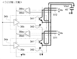
図5は、1個の圧電素子40を駆動するドライバー30の構成の一例を示す図である。
この図に示されるように、ドライバー30は、オペアンプ32と、単位回路34a〜34fと、コンパレーター38au、38ad、38bu、38bd、38cu、38cd、38du、38dd、38eu、38edとを含み、制御信号Vinにしたがって圧電素子40を駆動する構成となっている。
ドライバー30は、電圧ゼロを含めると、7種類の電圧、詳細には低い順に電圧ゼロ(グランドG)、VH/6、2VH/6、3VH/6、4VH/6、5VH/6、VHを用いる。
このうち、電圧ゼロおよび電圧VHを除いた5種類の電圧は、それぞれ電源配線511、512、513、514、515を介して補助電源回路50から供給される。
FIG. 5 is a diagram illustrating an example of the configuration of the
As shown in this figure, the
The
Of these, five types of voltages excluding the voltage zero and the voltage VH are supplied from the auxiliary
ドライバー30の入力端であるオペアンプ32の入力端(+)には、選択部230から出力される制御信号Vinが供給される。オペアンプ32の出力信号は、単位回路34a〜34fにそれぞれ供給されるとともに、抵抗Rfを介してオペアンプ32の入力端(−)に負帰還され、さらに抵抗Rinを介してグランドGに接地される。このため、オペアンプ32は、制御信号Vinを(1+Rf/Rin)倍に非反転増幅することになる。
オペアンプ32の電圧増幅率は、抵抗Rf、Rinによって設定することができるが、便宜上、以降においてはRfをゼロとし、Rinを無限大とする。すなわち、以降においては、オペアンプ32の電圧増幅率を「1」に設定して、制御信号Vinがそのまま単位回路34a〜34fに供給されるものとして説明する。なお、電圧増幅率が「1」以外であっても良い。
The control signal Vin output from the
The voltage amplification factor of the
単位回路34a〜34fは、上記7種類の電圧のうち、互いに隣り合う2つの電圧に対応して電圧の低い順に設けられる。詳細には、単位回路34aは電圧ゼロおよび電圧VH/6に対応し、単位回路34bは電圧VH/6および電圧2VH/6に対応し、単位回路34cは電圧2VH/6および電圧3VH/6に対応し、単位回路34dは電圧3VH/6および電圧4VH/6に対応し、単位回路34eは電圧4VH/6および電圧5VH/6に対応し、単位回路34fは電圧5VH/6および電圧VHに対応して設けられる。
The
単位回路34a〜34fの回路構成は互いに同じであり、レベルシフター36a〜36fのいずれか対応するもの1つと、バイポーラ型のNPN型のトランジスター341とPNP型のトランジスター342とを含む。
なお、単位回路34a〜34fについて、特定せずに一般的に説明するときには、単に符号を「34」として説明し、同様に、レベルシフター36a〜36fについて、特定せずに一般的に説明するときには、単に符号を「36」として説明する。
The
When the
レベルシフター36は、イネーブル(enable)状態とディセーブル(disable)状態とのいずれかの状態をとる。詳細には、レベルシフター36は、丸印が付された負制御端に供給される信号がLレベルであって、かつ、丸印が付されていない正制御端に供給される信号がHレベルであるときに、イネーブル状態になり、それ以外のときは、ディセーブル状態となる。 The level shifter 36 takes one of an enable state and a disable state. Specifically, in the level shifter 36, the signal supplied to the negative control end with a circle is L level, and the signal supplied to the positive control end with no circle is H level. Is in the enabled state, otherwise it is in the disabled state.
後述するように上記7種類の電圧のうち、電圧ゼロおよび電圧VHを除いた5種類の電圧のそれぞれには、コンパレーターのペアが関連している。詳細には、コンパレーターの符号38の直後の第1番目の符号a〜eは、それがaであれば電圧VH/6に、b〜eであれば、2VH/6、3VH/6、4VH/6、5VH/6に関連していることを示している。例えばコンパレーター38ad、38auのペアは電圧VH/6に関連し、また例えばコンパレーター38bd、38buのペアは電圧2VH/6に関連していることを示している。
さらに、コンパレーターのペアのそれぞれは、関連した電圧よりもαだけ低位の下側閾値電圧に対応しているものと、αだけ高位の高側閾値電圧に対応しているものとである。すなわち、コンパレーターの符号38の第2番目の符号d、uは、それがdであれば下側閾値電圧に対応していることを示し、uであれば高側閾値電圧に対応していることを示している。
したがって、例えばコンパレーター38auは、電圧VH/6よりもαだけ高位の高側閾値電圧に対応していることを示し、コンパレーター38bdは、電圧2VH/6よりもαだけ低位の低側閾値電圧に対応していることを示している。
なお、レベルシフターについて、特定せずに一般的に説明するときには、符号を省略して説明することにする。
Among the seven types of voltage as described later, each of the five voltages excluding the zero voltage and the voltage V H, the pair of the comparator is associated. Specifically, the first th code a~e immediately after the sign 38 of the comparator is that it the voltage V H / 6 if a, if b~e, 2V H / 6,3V H / to 6,4V H / 6,5V H / 6 indicates that it is relevant. For example, a pair of comparators 38ad, 38au is associated with voltage V H / 6, and a pair of comparators 38bd, 38bu is associated with voltage 2V H / 6, for example.
Further, each pair of comparators corresponds to a lower threshold voltage that is lower by α than the associated voltage and one that corresponds to a higher threshold voltage that is higher by α. That is, the second sign d, u of the sign 38 of the comparator indicates that if it is d, it corresponds to the lower threshold voltage, and if it is u, it corresponds to the higher threshold voltage. It is shown that.
Therefore, for example, the comparator 38au indicates that it corresponds to a higher threshold voltage that is higher by α than the voltage V H / 6, and the comparator 38bd has a lower side that is lower by α than the voltage 2V H / 6. It shows that it corresponds to the threshold voltage.
The level shifter will be described by omitting the reference numerals when it is generally described without being specified.
一方、ある単位回路34に着目したとき、当該単位回路34におけるレベルシフター36の負制御端には、当該単位回路34に対応した高位側電圧よりもαだけ高位の高側閾値電圧に対応したコンパレーターの出力信号が供給され、当該レベルシフター36の正制御端には、当該単位回路34に対応した低位側電圧よりもαだけ低位の低側閾値電圧に対応したコンパレーターの出力信号が供給される。例えば単位回路34bは、電圧VH/6および電圧2VH/6に対応している。このため、当該単位回路34bにおけるレベルシフター36bの負制御端には、高位側の電圧2VH/6の高側閾値電圧に対応したコンパレーター38buの出力信号が供給され、当該レベルシフター36bの正制御端には、低位側の電圧VH/6の下側閾値電圧に対応したコンパレーター38adの出力信号が供給される。
ただし、単位回路34fにおけるレベルシフター36fの負制御端はLレベルに相当する電圧ゼロのグランドGに接地される一方、単位回路34aにおけるレベルシフター36aの正制御端は、Hレベルに相当する電圧VHを供給する電源配線516に接続される。なお、単位回路34aにおけるレベルシフター36aの負制御端には、電圧VH/6の高側閾値電圧に対応しているコンパレーター38auの出力信号が供給されている。
On the other hand, when attention is paid to a certain unit circuit 34, a negative control terminal of the level shifter 36 in the unit circuit 34 has a comparator corresponding to a higher threshold voltage that is higher by α than the higher voltage corresponding to the unit circuit 34. The output signal of the comparator is supplied, and the output signal of the comparator corresponding to the lower threshold voltage lower by α than the lower voltage corresponding to the unit circuit 34 is supplied to the positive control terminal of the level shifter 36. The For example, the
However, the negative control terminal of the
レベルシフター36は、イネーブル状態では、入力された制御信号Vinの電圧をマイナス方向に所定値だけシフトさせてトランジスター341のベース端子に供給する一方、制御信号Vinの電圧をプラス方向に所定値だけシフトさせてトランジスター342のベース端子に供給する。レベルシフター36は、ディセーブル状態では、制御信号Vinにかかわらず、トランジスター341をオフさせる電圧、例えば電圧VHを当該トランジスター341のベース端子に供給するとともに、トランジスター342をオフさせる電圧、例えば電圧ゼロを当該トランジスター342のベース端子に供給する。
なお、本実施形態において所定値としては、エミッタ端子に電流が流れ始めるベース・エミッタ間の電圧(バイアス電圧、約0.6ボルト)としている。すなわち、レベルシフター36における所定値は、トランジスター341、342の特性に応じて定められる性質ものである。また、後述するように所定値としてはバイアス電圧以外に設定しても良い。
In the enabled state, the level shifter 36 shifts the voltage of the input control signal Vin in the minus direction by a predetermined value and supplies it to the base terminal of the
In the present embodiment, the predetermined value is a base-emitter voltage (bias voltage, approximately 0.6 volts) at which current starts to flow through the emitter terminal. That is, the predetermined value in the level shifter 36 has a property determined according to the characteristics of the
ある単位回路34におけるトランジスター341のコレクタ端子は、当該単位回路34に対応する2電圧のうち、高位側電圧を供給する電源配線に接続され、トランジスター342のコレクタ端子は、低位側電圧を供給する電源配線に接続される。例えば、電圧ゼロおよび電圧VH/6に対応する単位回路34aでは、トランジスター341のコレクタ端子が電圧VH/6を供給する電源配線511に接続され、トランジスター342のコレクタ端子が電圧ゼロのグランドGに接地される。また例えば、電圧VH/6および電圧2VH/6に対応する単位回路34bでは、トランジスター341のコレクタ端子が電圧2VH/6を供給する電源配線512に接続され、トランジスター342のコレクタ端子が電圧VH/6を供給する電源配線511に接続される。なお、電圧5VH/6および電圧VHに対応する単位回路34fでは、トランジスター341のコレクタ端子が電圧VHを供給する電源配線516に接続され、トランジスター342のコレクタ端子が電圧5VH/6を供給する電源配線515に接続される。
The collector terminal of the
一方、単位回路34a〜34fにおいてトランジスター341、342の各エミッタ端子は、圧電素子40の一端に共通接続される。このため、上述したようにトランジスター341、342の各エミッタ端子の共通接続点が、ドライバー30の出力端として圧電素子40の一端に接続されることになる。
On the other hand, the emitter terminals of the
コンパレーターのペアは、7種類の電圧のうち、電圧ゼロおよび電圧VHを除いた5種類の電圧のそれぞれに関連し、各ペアは、関連した電圧よりもαだけ低位の下側閾値電圧に対応したコンパレーターと、αだけ高位の高側閾値電圧に対応したコンパレーターとで構成される。
各コンパレーターは、2つの入力端を有し、このうち、一端には自身に対応付けられた閾値電圧が供給され、他端には、トランジスター341、342の各エミッタ端子および圧電素子40の一端の接続部分における電圧Voutが供給される。
各コンパレーターは、入力端における他端の電圧Voutが一端の閾値電圧以上であればHレベルとし、電圧Voutが一端の閾値電圧未満であればLレベルとした信号を出力する。具体的には例えばコンパレーター38adは、電圧Voutが閾値電圧(VH/6−α)以上であればHレベルとし、閾値電圧(VH/6−α)未満であればLレベルとした信号を出力する。また例えば、コンパレーター38buは、電圧Voutが電圧(2VH/6+α)以上であればHレベルとし、電圧(2VH/6+α)未満であればLレベルとした信号を出力する。なお、各コンパレーターの出力信号の供給先は、すでに説明した通りである。
また、図5においては、各コンパレーターの入力端の一端には、自身に対応付けられた電圧が供給されているかのように図示されているが、実際には、入力端の一端に供給された電圧を内部でαだけレベルシフトするとともに、レベルシフトした電圧を閾値電圧として電圧Voutと比較する構成となっている(後述する図20、図21においても同じ)。
A pair of comparators is associated with each of five of the seven voltages except voltage zero and voltage V H , and each pair has a lower threshold voltage that is α lower than the associated voltage. It is composed of a corresponding comparator and a comparator corresponding to a high threshold voltage that is higher by α.
Each comparator has two input terminals, one of which is supplied with a threshold voltage associated with itself, and the other terminal is connected to each emitter terminal of the
Each comparator outputs a signal that is at the H level if the voltage Vout at the other end at the input end is equal to or higher than the threshold voltage at one end, and is at the L level if the voltage Vout is less than the threshold voltage at one end. The comparator 38ad example Specifically, if the voltage Vout the threshold voltage (V H / 6-α) or more as the H level, and the threshold voltage (V H / 6-α) is less than L-level signal Is output. Further, for example, comparator 38bu, the voltage Vout is set to the H level if the voltage (2V H / 6 + α) or more, and outputs an L level signal is less than the voltage (2V H / 6 + α) . The supply destination of the output signal of each comparator is as described above.
In FIG. 5, one end of each comparator input terminal is shown as if a voltage associated with itself is supplied, but in reality, it is supplied to one end of the input terminal. The voltage is internally level-shifted by α and compared with the voltage Vout using the level-shifted voltage as a threshold voltage (the same applies to FIGS. 20 and 21 described later).
次に、ドライバー30の動作について説明する。
まず、圧電素子40で保持された電圧Voutに対して、レベルシフター36a〜36fがどのような状態になるのかについて検討する。
Next, the operation of the
First, the state of the
図6は、レベルシフター36a〜36fが電圧Voutに対してイネーブル状態となる電圧の範囲を示す図である。
電圧Voutが電圧ゼロ以上閾値電圧(VH/6−α)未満であるD1状態において、コンパレーターの出力信号はすべてLレベルとなる。このため、D1状態では、レベルシフター36aのみがイネーブル状態になり、他のレベルシフター36b〜36fはディセーブル状態になる。
電圧Voutが閾値電圧(VH/6−α)以上閾値電圧(VH/6+α)未満であるD2状態において、コンパレーター38adの出力信号だけがHレベルとなり、他のコンパレーターの出力信号はLレベルとなる。したがって、D2状態では、レベルシフター36a、36bがともにイネーブル状態になり、他のレベルシフター36c〜36fはディセーブル状態になる。
FIG. 6 is a diagram illustrating a voltage range in which the
In the D1 state where the voltage Vout is equal to or higher than the voltage zero and lower than the threshold voltage (V H / 6−α), all output signals of the comparators are L level. Therefore, in the D1 state, only the
In the D2 state where the voltage Vout is greater than or equal to the threshold voltage ( VH / 6-α) and less than the threshold voltage ( VH / 6 + α), only the output signal of the comparator 38ad becomes H level, and the output signals of the other comparators are L Become a level. Therefore, in the D2 state, the
電圧Voutが閾値電圧(VH/6+α)以上閾値電圧(2VH/6−α)未満であるD3状態において、コンパレーター38ad、38auの出力信号がともにHレベルとなり、他のコンパレーターの出力信号はLレベルとなる。したがって、D3状態では、レベルシフター36bだけがイネーブル状態になり、他のレベルシフター36a、36c〜36fはディセーブル状態になる。
電圧Voutが閾値電圧(2VH/6−α)以上閾値電圧(2VH/6+α)未満であるD4状態において、コンパレーター38ad、38au、38bdの出力信号がHレベルとなり、他のコンパレーターの出力信号はLレベルとなる。したがって、D4状態では、レベルシフター36b、36cがともにイネーブル状態になり、他のレベルシフター36a、36d〜36fはディセーブル状態になる。
In the D3 state is less than the voltage Vout the threshold voltage (V H / 6 + α) than the threshold voltage (2V H / 6-α) , comparator 38Ad, the output signal of 38au both attain an H level, the output signal of the other comparator Becomes L level. Accordingly, in the D3 state, only the
In D4 state is less than the voltage Vout the threshold voltage (2V H / 6-α) equal to or higher than the threshold voltage (2V H / 6 + α) , the comparator 38ad, 38au, the output signal of the 38bd becomes H level, the other comparator output The signal becomes L level. Accordingly, in the D4 state, the
以降詳細については省略するが、D5状態からD11状態まで、コンパレーターの出力信号は、閾値電圧が低いものの順にHレベルとなる。
このため、電圧Voutが閾値電圧(2VH/6+α)以上閾値電圧(3VH/6−α)未満のD5状態では、レベルシフター36cだけがイネーブル状態になり、他のレベルシフター36a、36b、36d〜36fはディセーブル状態になる。
電圧Voutが閾値電圧(3VH/6−α)以上閾値電圧(3VH/6+α)未満のD6状態では、レベルシフター36c、36dがともにイネーブル状態になり、他のレベルシフター36a、36b、36e、36fはディセーブル状態になる。
電圧Voutが閾値電圧(3VH/6+α)以上閾値電圧(4VH/6−α)未満のD7状態では、レベルシフター36dだけがイネーブル状態になり、他のレベルシフター36a〜36c、36e、36fはディセーブル状態になる。
電圧Voutが閾値電圧(4VH/6−α)以上閾値電圧(4VH/6+α)未満のD8状態では、レベルシフター36d、36eがともにイネーブル状態になり、他のレベルシフター36a〜36c、36fはディセーブル状態になる。
電圧Voutが閾値電圧(4VH/6+α)以上閾値電圧(5VH/6−α)未満のD9状態では、レベルシフター36eだけがイネーブル状態になり、他のレベルシフター36a〜36d、36fはディセーブル状態になる。
電圧Voutが閾値電圧(5VH/6−α)以上閾値電圧(5VH/6+α)未満のD10状態では、レベルシフター36e、36fがともにイネーブル状態になり、他のレベルシフター36a〜36dはディセーブル状態になる。
電圧Voutが閾値電圧(5VH/6+α)以上閾値電圧VH未満のD11状態では、レベルシフター36fだけがイネーブル状態になり、他のレベルシフター36a〜36eはディセーブル状態になる。
なお、D1状態からD11状態までについては電圧Voutで規定しているが、これは、圧電素子40に保持(蓄積)された電荷の状態と言い換えることができる。
Although not described in detail later, the output signal of the comparator becomes H level in the order of the lowest threshold voltage from the D5 state to the D11 state.
Therefore, in the D5 state in which the voltage Vout is equal to or higher than the threshold voltage (2V H / 6 + α) and lower than the threshold voltage (3V H / 6−α), only the
In the D6 state where the voltage Vout is greater than or equal to the threshold voltage (3V H / 6−α) and less than the threshold voltage (3V H / 6 + α), the
In the D7 state in which the voltage Vout is greater than or equal to the threshold voltage (3V H / 6 + α) and less than the threshold voltage (4V H / 6−α), only the
In the D8 state where the voltage Vout is greater than or equal to the threshold voltage (4V H / 6−α) and less than the threshold voltage (4V H / 6 + α), the
In the D9 state where the voltage Vout is equal to or higher than the threshold voltage (4V H / 6 + α) and lower than the threshold voltage (5V H / 6−α), only the
The D10 state of less than the voltage Vout the threshold voltage (5V H / 6-α) equal to or higher than the threshold voltage (5V H / 6 + α) , the
In the D11 state where the voltage Vout is equal to or higher than the threshold voltage (5V H / 6 + α) and lower than the threshold voltage V H , only the
The voltage from the D1 state to the D11 state is defined by the voltage Vout, which can be rephrased as the state of charges held (accumulated) in the
さて、例えば上記D1状態においてレベルシフター36aがイネーブル状態のとき、当該レベルシフター36aは、制御信号Vinをマイナス方向に所定値だけレベルシフトした電圧信号を単位回路34aにおけるトランジスター341のベース端子に供給し、制御信号Vinをプラス方向に所定値だけレベルシフトした電圧信号を当該単位回路34aにおけるトランジスター342のベース端子に供給する。
For example, when the
ここで、制御信号Vinの電圧が電圧Vout(エミッタ端子同士の接続点電圧)よりも高いとき、その差(ベース・エミッタ間の電圧、厳密にいえばベース・エミッタ間の電圧から所定値だけ減じた電圧)に応じた電流がトランジスター341のコレクタ端子からエミッタ端子に流れる。このため、電圧Voutが徐々に上昇して制御信号Vinの電圧に近づき、やがて電圧Voutが制御信号Vinの電圧に一致すると、その時点でトランジスター341に流れていた電流がゼロになる。
Here, when the voltage of the control signal Vin is higher than the voltage Vout (connection voltage between the emitter terminals), the difference (the voltage between the base and the emitter, strictly speaking, the voltage between the base and the emitter is reduced by a predetermined value. Current corresponding to the voltage) flows from the collector terminal of the
一方、D1状態において制御信号Vinの電圧が電圧Voutよりも低いとき、その差に応じた電流がトランジスター342のエミッタ端子からコレクタ端子に流れる。このため、電圧Voutが徐々に低下して制御信号Vinの電圧に近づき、やがて電圧Voutが制御信号Vinの電圧に一致すると、その時点でトランジスター342に流れる電流がゼロになる。
したがって、D1状態において、電圧Voutを制御信号Vinに一致させるような制御が実行されることになる。
On the other hand, when the voltage of the control signal Vin is lower than the voltage Vout in the D1 state, a current corresponding to the difference flows from the emitter terminal of the
Therefore, in the D1 state, control is performed so that the voltage Vout matches the control signal Vin.
D1状態において、単位回路34a以外の単位回路34b〜34fでは、レベルシフター36がディセーブル状態となるので、トランジスター341のベース端子には電圧VHが供給され、トランジスター342のベース端子には電圧ゼロが供給される。このため、D1状態において、単位回路34b〜34fでは、トランジスター341、342がオフするので、電圧Voutの制御には関与しないことになる。
ここでは、D1状態であるときについて説明しているが、D3状態、D5状態、D7状態、D9状態、D11状態についても同様な動作となる。詳細には、圧電素子40で保持された電圧Voutに応じて、単位回路34a〜34fのいずれか1つが有効になるとともに、有効になった単位回路のトランジスター341、342が電圧Voutを制御信号Vinに一致させるように制御する。
In the D1 state, in the
Here, the case of the D1 state has been described, but the same operation is performed for the D3 state, the D5 state, the D7 state, the D9 state, and the D11 state. Specifically, according to the voltage Vout held by the
次にD2状態について説明する。上記D2状態においてレベルシフター36a、36bがともにイネーブル状態のとき、レベルシフター36aは、制御信号Vinをマイナス方向に所定値だけレベルシフトした電圧信号を単位回路34aにおけるトランジスター341のベース端子に供給し、制御信号Vinをプラス方向に所定値だけレベルシフトした電圧信号を当該単位回路34aにおけるトランジスター342のベース端子に供給する。ここまでは、D1状態と同様であるが、D2状態ではさらに、レベルシフター36bが、制御信号Vinをマイナス方向に所定値だけレベルシフトした電圧信号を単位回路34bにおけるトランジスター341のベース端子に供給し、制御信号Vinをプラス方向に所定値だけレベルシフトした電圧信号を当該単位回路34bにおけるトランジスター342のベース端子に供給する。
Next, the D2 state will be described. When the
ここで、D2状態において制御信号Vinの電圧が電圧Voutよりも高いとき、その差に応じた電流が単位回路34aにおけるトランジスター341のコレクタ端子からエミッタ端子に流れるとともに、単位回路34bにおけるトランジスター341のコレクタ端子からエミッタ端子に流れる。すなわち、D2状態において制御信号Vinの電圧が電圧Voutよりも高いとき、2つのトランジスター341によって圧電素子40に向けて電流が流れる。このため、電圧Voutが徐々に上昇して制御信号Vinの電圧に近づき、やがて電圧Voutが制御信号Vinの電圧に一致すると、その時点で2つのトランジスター341に流れていた電流がゼロになる。
したがって、D2状態においても、電圧Voutを制御信号Vinに一致させるような制御が実行されることになる。
Here, when the voltage of the control signal Vin is higher than the voltage Vout in the D2 state, a current corresponding to the difference flows from the collector terminal of the
Therefore, even in the D2 state, control is performed so that the voltage Vout matches the control signal Vin.
D2状態においてレベルシフター36aによって制御信号Vinをマイナス方向にレベルシフトされた電圧は、すなわち単位回路34aにおけるトランジスター341のベース端子に供給される電圧は、当該トランジスター341のコレクタ端子の電圧VHに近い。D2状態において、制御信号Vinの上昇に対して電圧Voutを一致させる制御が実行される結果、制御信号Vinの電圧と電圧Voutとが近接したとき、単位回路34aにおけるトランジスター341のベース・エミッタ間の電圧は、非常に小さくなる。このため、単位回路34aにおけるトランジスター341の単体だけでみれば、電流がエミッタ端子から(圧電素子40に向けて)流れ出しにくい状況にある、ということができる。
ただし、本実施形態では、D2状態においてはレベルシフター36aだけでなくレベルシフター36bもイネーブル状態にある。D2状態においてレベルシフター36bによって制御信号Vinをマイナス方向にレベルシフトされた電圧は、すなわち単位回路34bにおけるトランジスター341のベース端子に供給される電圧は、当該トランジスター341のコレクタ端子の電圧2VH/6とは離れている上に、当該トランジスター341のベース・エミッタ間の電圧についても、単位回路34aのトランジスター341と比較して大きい。このため、単位回路34bにおけるトランジスター341では、単位回路34aにおけるトランジスター341と比較して、電流が流れ出しやすい状況にある、ということができる。
Voltage control signal Vin by the
However, in the present embodiment, not only the
一方、D2状態においてレベルシフター36bによって制御信号Vinをプラス方向にレベルシフトされた電圧は、すなわち単位回路34bにおけるトランジスター342のベース端子に供給される電圧は、当該トランジスター342のコレクタ端子の電圧VHに近い。D2状態において、制御信号Vinの下降に対して電圧Voutを一致させる制御が実行される結果、制御信号Vinの電圧と電圧Voutとが近接したとき、単位回路34bにおけるトランジスター342のベース・エミッタ間の電圧は、非常に小さくなる。このため、単位回路34bにおけるトランジスター342の単体だけでみれば、電流が(圧電素子40から)エミッタ端子に向けて電流が流れ込みにくい状況にある、ということができる。
ただし、本実施形態では、D2状態においてレベルシフター36aもイネーブル状態にあるので、レベルシフター36aによって制御信号Vinをプラス方向にレベルシフトされた電圧は、すなわち単位回路34aにおけるトランジスター342のベース端子に供給される電圧は、当該トランジスター342のコレクタ端子の電圧ゼロとは離れている上に、当該トランジスター342のベース・エミッタ間の電圧についても、単位回路34bのトランジスター341と比較して大きい。このため、単位回路34aにおけるトランジスター342では、単位回路34bにおけるトランジスター342と比較して、電流が流れ込みやすい状況にある、ということができる。
On the other hand, the voltage obtained by level shifting the control signal Vin in the positive direction by the
However, in this embodiment, since the
したがって、本実施形態において、電圧Voutが電圧VHに対して±αの範囲にあるD2状態では、圧電素子40が充電しにくくなることもなければ、圧電素子40を放電しにくくなるということもない。
なお、D2状態において、単位回路34a、34b以外の単位回路34c〜34fでは、トランジスター341、342がオフするので、電圧Voutの制御には関与しないことになる。
またここでは、D2状態であるときについて説明しているが、D4状態、D6状態、D8状態、D10状態についても同様な動作となる。詳細には、圧電素子40で保持された電圧Voutに応じて、単位回路34a〜34fのうち、隣り合う2つが有効になるとともに、有効になった単位回路34のトランジスター341、342が電圧Voutを制御信号Vinに一致させるように制御する。
Accordingly, in the present embodiment, the D2 state in the range of ± alpha voltage Vout relative to the voltage V H, if also the
In the D2 state, in the
Further, here, the case of the D2 state has been described, but the same operation is performed for the D4 state, the D6 state, the D8 state, and the D10 state. Specifically, according to the voltage Vout held by the
ドライバー30の全体としてみたときに、D1状態〜D11状態では、電圧Voutが、制御信号Vinの電圧に追従する動作となる。
したがって、図7の(a)に示されるように、制御信号Vinが例えば電圧ゼロから電圧VHまで上昇するとき、電圧Voutも制御信号Vinに追従して電圧ゼロから電圧VHまで変化する。また、同図の(b)に示されるように、制御信号Vinが電圧VHから電圧ゼロまで低下するとき、電圧Voutも制御信号Vinに追従して電圧VHから電圧ゼロまで変化する。
When the
Thus, as shown in (a) of FIG. 7, when the control signal Vin to increase, for example, from voltage zero to the voltage V H, is changed from zero voltage to the voltage V H to follow the voltage Vout to the control signals Vin. Further, as shown in FIG. 5B, when the control signal Vin decreases from the voltage VH to the voltage zero, the voltage Vout also changes from the voltage VH to the voltage zero following the control signal Vin.
図8および図9は、レベルシフターの動作を説明するための図である。
制御信号Vinの電圧が電圧ゼロから電圧VHまで上昇するとき、電圧Voutも制御信号Vinに追従して上昇する。この上昇の過程において、電圧Voutが閾値電圧(VH/6+α)未満であるとき、レベルシフター36aがイネーブル状態になる。このため、図8の(a)で示されるように、レベルシフター36aによってトランジスター341のベース端子に供給される電圧(図において「P型」と表記)は、制御信号Vinをマイナス方向に所定値だけシフトさせた電圧となり、トランジスター342のベース端子に供給される電圧(N型と表記)は、制御信号Vinをプラス方向に所定値だけシフトさせた電圧となる。
一方、電圧Voutが閾値電圧(VH/6+α)以上であるとき、レベルシフター36aがディセーブル状態になるので、トランジスター341のベース端子に供給される電圧はVHとなり、トランジスター342のベース端子に供給される電圧はゼロとなる。
電圧Voutの上昇過程において、同図の(b)はレベルシフター36bが出力する電圧波形を示し、同図の(c)はレベルシフター36fが出力する電圧波形を示す。
8 and 9 are diagrams for explaining the operation of the level shifter.
When the voltage of the control signal Vin is increased from zero voltage to the voltage V H, the voltage Vout rises to follow the control signal Vin. In the course of this increase, when the voltage Vout is less than the threshold voltage (V H / 6 + α), the
On the other hand, when the voltage Vout is equal to or higher than the threshold voltage (V H / 6 + α), the
In the process of increasing the voltage Vout, (b) in the figure shows the voltage waveform output from the
反対に、制御信号Vinの電圧が電圧VHから電圧ゼロまで低下するとき、電圧Voutも制御信号Vinに追従して低下する。この低下の過程において、図9の(a)はレベルシフター36aが出力する電圧波形を示し、同図の(b)はレベルシフター36bが出力する電圧波形を示し、同図の(c)はレベルシフター36fが出力する電圧波形を示す。
Conversely, when the voltage of the control signal Vin decreases from the voltage VH to the voltage zero, the voltage Vout also decreases following the control signal Vin. 9A shows a voltage waveform output from the
レベルシフター36bについては、電圧Voutが閾値電圧(VH/6−α)以上閾値電圧(2VH/6+α)未満であるときにイネーブル状態になり、レベルシフター36fについては、電圧Voutが閾値電圧(5VH/6−α)以上電圧VH未満であるときにイネーブル状態になる点に留意すれば、出力する電圧波形についての特段の説明は要しないであろう。
また、制御信号Vinの電圧(または電圧Vout)の変化に対するレベルシフター36c〜36eの動作についての説明についても省略する。
The
Further, the description of the operation of the
次に、単位回路34a〜34fにおける電流(電荷)の流れについて、単位回路34a、34bを例にとり、充電時と放電時とにわけてそれぞれに説明する。
Next, the flow of current (charge) in the
図10は、D1状態、すなわち電圧Voutが電圧ゼロ以上閾値電圧(VH/6−α)未満の状態であるときに、圧電素子40が充電されるときの動作を示す図である。
D1状態では、レベルシフター36aだけがイネーブル状態になり、他のレベルシフター36b〜36fはディセーブル状態になるので、単位回路34aのみに着目すれば良い。D1状態において制御信号Vinの電圧が電圧Voutよりも高いとき、単位回路34aのトランジスター341はベース・エミッタ間の電圧に応じた電流を流す。このときに、電流は、図において矢印で示されるように電源配線511→(単位回路34aの)トランジスター341→圧電素子40という経路で流れて、これにより、圧電素子40に電荷が充電される。この充電により電圧Voutが上昇する。
FIG. 10 is a diagram illustrating an operation when the
In the D1 state, only the
なお、電圧Voutが制御信号Vinの電圧に一致したとき、単位回路34aのトランジスター341がオフするので、圧電素子40への充電が停止する。一方で、制御信号Vinが閾値電圧(VH/6−α)以上に上昇するとき、電圧Voutも制御信号Vinに追従して閾値電圧(VH/6−α)以上になるので、D1状態からD2状態に移行する。
Note that when the voltage Vout matches the voltage of the control signal Vin, the
図11は、D2状態、すなわち電圧Voutが閾値電圧(VH/6−α)以上閾値電圧(VH/6+α)未満の状態であるときに、圧電素子40が充電されるときの動作を示す図である。
D2状態では、レベルシフター36a、36bがともにイネーブル状態になるので、単位回路34a、34bに着目する必要がある。
D2状態において制御信号Vinの電圧が電圧Voutよりも高いとき、単位回路34aにおけるトランジスター341はベース・エミッタ間の電圧に応じた電流を流し、同様に、単位回路34bにおけるトランジスター342もベース・エミッタ間の電圧に応じた電流を流す。このときに、電流は、図において矢印で示されるように電源配線511→(単位回路34aの)トランジスター341→圧電素子40という経路のほかに、電源配線512→(単位回路34bの)トランジスター341→圧電素子40という経路の2つによって流れて、これにより、圧電素子40に電荷が充電される。この充電により電圧Voutが上昇する。
このように、電圧Voutの上昇時においてD1状態からD2状態に移行すると、電流の供給元が電源配線511のみの1経路から、電源配線512を併用した2経路へと切り替わる。
FIG. 11 shows an operation when the
Since the
When the voltage of the control signal Vin is higher than the voltage Vout in the D2 state, the
As described above, when the voltage Vout is increased, when the state transitions from the D1 state to the D2 state, the current supply source is switched from one path having only the
なお、電圧Voutが制御信号Vinの電圧に一致したとき、単位回路34aにおけるトランジスター341と、単位回路34bにおけるトランジスター341とはともにオフするので、圧電素子40への充電が停止する。一方で、制御信号Vinが閾値電圧(VH/6+α)以上に上昇するとき、電圧Voutも制御信号Vinに追従して閾値電圧(VH/6+α)以上になるので、D2状態からD3状態に移行する。
When the voltage Vout matches the voltage of the control signal Vin, the
図12は、D3状態、すなわち電圧Voutが閾値電圧(VH/6+α)以上閾値電圧(2VH/6−α)の状態であるときに、圧電素子40が充電されるときの動作を示す図である。
D3状態では、レベルシフター36bだけがイネーブル状態になるので、単位回路34bのみに着目すれば良い。D3状態において制御信号Vinの電圧が電圧Voutよりも高いとき、単位回路34bのトランジスター341はベース・エミッタ間の電圧に応じた電流を流す。このときに、電流は、図において矢印で示されるように電源配線512→(単位回路34bの)トランジスター341→圧電素子40という経路で流れて、これにより、圧電素子40に電荷が充電される。この充電により電圧Voutが上昇する。
このように、電圧Voutの上昇時においてD2状態からD3状態に移行すると、電流の供給元が電源配線511、512を併用した2経路から、電源配線512のみの1経路へと切り替わる。
FIG. 12 is a diagram showing an operation when the
Since only the
As described above, when the voltage Vout is increased and the state is changed from the D2 state to the D3 state, the current supply source is switched from the two paths using the
電圧Voutが制御信号Vinに一致したとき、単位回路34bのトランジスター341がオフするので、圧電素子40への充電が停止する。一方で、制御信号Vinが閾値電圧(2VH/6−α)以上に上昇すれば、電圧Voutも制御信号Vinに追従して上昇する。
そして、電圧Voutが閾値電圧を超えるごとにD4状態からD11状態まで段階的に移行する。
When the voltage Vout matches the control signal Vin, the
Then, every time the voltage Vout exceeds the threshold voltage, a transition is made in stages from the D4 state to the D11 state.
図13は、D3状態のときに、圧電素子40が放電するときの動作を示す図である。
D3状態では、レベルシフター36bだけがイネーブル状態になる。この状態において、制御信号Vinが電圧Voutよりも低いとき、単位回路34bのトランジスター342はベース・エミッタ間の電圧に応じた電流を流す。このとき、電流は、図において矢印で示されるように、圧電素子40→(単位回路34bの)トランジスター342→電源配線511という経路で流れて、これにより、圧電素子40から電荷が放電される。このため、D3状態において圧電素子40から電荷が放電されるとき、圧電素子40の一端は、電源配線511に当該トランジスター342を介して電気的に接続されて、圧電素子40からの電流(電荷)が補助電源回路50に回収されることになる。なお、回収された電荷は、後述する補助電源回路50によって再分配、再利用される。
また、電圧Voutが制御信号Vinの電圧に一致したとき、単位回路34bのトランジスター342がオフするので、圧電素子40からの放電が停止する。
一方で、制御信号Vinが閾値電圧(VH/6+α)未満に低下するとき、電圧Voutも制御信号Vinに追従して閾値電圧(VH/6+α)未満になるので、D3状態からD2状態に移行する。
FIG. 13 is a diagram illustrating an operation when the
In the D3 state, only the
Further, when the voltage Vout matches the voltage of the control signal Vin, the
On the other hand, when the control signal Vin falls below the threshold voltage (V H / 6 + α), the voltage Vout also follows the control signal Vin and falls below the threshold voltage (V H / 6 + α), so that the D3 state is changed to the D2 state. Transition.
図14は、D2状態、すなわち電圧Voutが閾値電圧(VH/6−α)以上閾値電圧(VH/6+α)であるときに、圧電素子40が放電するときの動作を示す図である。
D2状態では、レベルシフター36a、36bがともにイネーブル状態になるので、単位回路34a、34bに着目する必要がある。 D2状態において制御信号Vinの電圧が電圧Voutよりも低いとき、単位回路34bにおけるトランジスター342はベース・エミッタ間の電圧に応じた電流を流し、同様に、単位回路34aにおけるトランジスター342もベース・エミッタ間の電圧に応じた電流を流す。このときに、電流は、図において矢印で示されるように圧電素子40→(単位回路34bの)トランジスター342→電源配線511という経路のほかに、圧電素子40→(単位回路34aの)トランジスター342→グランドGという経路の2つによって流れて、これにより、圧電素子40の電荷が放電される。このため、単位回路34aにおけるトランジスター342がトランジスターAとして機能し、単位回路34bにおけるトランジスター342がトランジスターBとして機能する。このようにD2状態において圧電素子40から電荷が放電されるとき、圧電素子40の一端は、2つのトランジスター342を介して電源配線511およびグランドGに電気的に接続されて、このうち、電源配線511を介して電荷が補助電源回路50に回収されることになる。なお、回収された電荷は、後述する補助電源回路50によって再分配、再利用される。
このように、電圧Voutの下降時においてD3状態からD2状態に移行すると、電荷の回収先が電源配線511のみの1経路から、グランドGを併用した2経路へと切り替わる。
FIG. 14 is a diagram illustrating an operation when the
Since the
As described above, when the voltage Vout is lowered and the state is changed from the D3 state to the D2 state, the charge collection destination is switched from one path having only the
電圧Voutが制御信号Vinの電圧に一致したとき、単位回路34bにおけるトランジスター342と、単位回路34aにおけるトランジスター342とはともにオフするので、圧電素子40からの放電が停止する。
一方で、制御信号Vinが閾値電圧(VH/6+α)未満に低下するとき、電圧Voutも制御信号Vinに追従して閾値電圧(VH/6+α)未満になるので、D2状態からD1状態に移行する。
When the voltage Vout matches the voltage of the control signal Vin, the
On the other hand, when the control signal Vin falls below the threshold voltage (V H / 6 + α), the voltage Vout also follows the control signal Vin and falls below the threshold voltage (V H / 6 + α). Transition.
図15は、D1状態のときに、圧電素子40が放電するときの動作を示す図である。
D1状態では、レベルシフター36aがイネーブル状態になる。この状態において、制御信号Vinが電圧Voutよりも低いとき、単位回路34aのトランジスター342はベース・エミッタ間の電圧に応じた電流を流す。このとき、電流は、図において矢印で示されるように、圧電素子40→(単位回路34aの)トランジスター342→グランドGという経路で流れて、これにより、圧電素子40から電荷が放電される。
FIG. 15 is a diagram illustrating an operation when the
In the D1 state, the
なおここでは、単位回路34a、34bを例にとって、D1状態、D2状態およびD3状態につき充電時と放電時とにわけて説明したが、D4状態〜D11状態にあるときの単位回路34c〜34fについての動作も、ほぼ同様となる。
Here, the
<ドライバーの利点>
一般に、圧電素子40のような容量性負荷の容量をCとし、電圧振幅をEとしたときに、容量性負荷に蓄えられるエネルギーPは、
P=(C・E2)/2
で表される。
圧電素子40は、このエネルギーPによって変形して仕事をするが、インクを吐出させる仕事量は、エネルギーPに対して1%以下である。したがって、圧電素子40は、単なる容量とみなすことができる。容量Cを一定の電源で充電すると、(C・E2)/2と同等のエネルギーが充電回路によって消費される。放電するときにも同等のエネルギーが放電回路によって消費される。
<Advantages of driver>
In general, when the capacity of a capacitive load such as the
P = (C · E 2 ) / 2
It is represented by
The
本実施形態において、圧電素子40を電圧ゼロから電圧VHまで充電するときに、電荷を供給する電源配線については、一部に2経路で重複する状態があるが、基本的には電源配線511、512、513、514、515、516という順番で切り替わる。このため、本実施形態において充電時の損失は、図16の(a)においてハッチングが付された領域の面積に相当する分で済む。詳細には、本実施形態において圧電素子40において充電時の損失は、電圧ゼロから電圧VHまで一気に充電するリニア増幅と比較して、6/36(=16.7%)で済む。
一方、本実施形態では、放電時においても段階的となるので、放電時の損失は、図16の(b)においてハッチングが付された領域の面積に相当する分で示されるように、電圧VHから電圧ゼロまで一気に放電するリニア方式と比較して、同様に6/36(=16.7%)で済む。
ただし、本実施形態では、放電時の損失として計上された電荷のうち、電圧VH/6から電圧ゼロまで放電する場合を除き、後述する補助電源回路50に回収されて再分配、再利用されるので、さらなる低消費電力化を図ることができる。
なお、図16は、ドライバー30よる圧電素子40の駆動動作を説明するための概念図に過ぎない。圧電素子40は、実際には、制御信号COMのうち、駆動パルスPCOM1からPCOM4までのうち選択されたもので駆動されるので、常に電圧ゼロから電圧VHまでの振幅で駆動されるわけではない。
In the present embodiment, when the
On the other hand, in this embodiment, since it becomes stepwise even at the time of discharge, the loss at the time of discharge is represented by the voltage V V as shown by the amount corresponding to the area of the hatched area in FIG. Compared with the linear system that discharges at a stroke from H to zero voltage, 6/36 (= 16.7%) is sufficient.
However, in the present embodiment, out of the charge counted as a loss at the time of discharge, except for the case of discharging from the voltage V H / 6 to the voltage zero, it is recovered by the auxiliary
FIG. 16 is only a conceptual diagram for explaining the driving operation of the
ところで、D級増幅では、リニア増幅として比較してエネルギー効率が高い。その理由は、出力段の能動素子が飽和状態で動作し、電力をほとんど消費しない点、ローパスフィルターを構成するインダクターLによる磁気エネルギーと容量Cによるエネルギーとの交換によって充電時にはリニア増幅のような損失が発生しない点、放電時の電流スイッチングで電流が電源に回生する点などのためである。
しかしながら、実際のD級増幅では、出力段の能動素子の抵抗は、飽和状態でもゼロではない、磁界が漏れる、インダクターLの抵抗成分によって損失が発生する、変調時にインダクターLが飽和する場合がある、などの問題がある。特に、印刷ヘッド20において共通の制御信号COMから選択部230で選択して複数の圧電素子40に供給する構成では、制御信号COMからみた負荷容量の総量が一定でないので、飽和しないインダクターLが増える。
D級増幅では、さらに波形品質が悪い、EMIの対策が必要である、という問題がある。波形品質については、ダミーの容量やフィルターを追加することによって改善することができるが、追加した分だけ消費電力の増加やコスト高を招く。EMIについては、D級増幅のスイッチングという根本的な問題による。すなわち、スイッチングしたときに、オン時に流れる電流がリニア増幅と比較して数倍から10数倍程度までになるだけでなく、これに伴って放射される磁界の量も多くなるからである。EMIの対策のために、フィルターを追加するなどが必要となり、コスト高を招く。
By the way, in class D amplification, energy efficiency is higher than linear amplification. The reason is that the active element in the output stage operates in a saturated state and consumes almost no power, and a loss such as linear amplification at the time of charging by exchanging magnetic energy by the inductor L constituting the low-pass filter and energy by the capacitor C. This is because no current is generated, and current is regenerated to the power supply by current switching during discharge.
However, in actual class D amplification, the resistance of the active element in the output stage is not zero even in a saturated state, the magnetic field leaks, loss occurs due to the resistance component of the inductor L, and the inductor L may be saturated during modulation. , Etc. In particular, in the configuration in which the
In class D amplification, there are problems that the waveform quality is further poor and EMI countermeasures are required. The waveform quality can be improved by adding a dummy capacity or a filter, but this increases the power consumption and costs. EMI is due to the fundamental problem of class D amplification switching. That is, when the switching is performed, not only does the current flowing at the time of on-state increase from several times to about several tens of times compared to the linear amplification, but the amount of the magnetic field radiated increases accordingly. For measures against EMI, it is necessary to add a filter or the like, resulting in high costs.
本実施形態に係る印刷装置1のドライバー30では、出力段に相当するトランジスター341、342は、D級増幅のようなスイッチングをしないので、また、インダクターLが用いられていないので、波形品質が悪い、EMIの対策が必要である、という問題が発生しない。
また、本実施形態では、電圧Voutについて、単なる電圧VH/6、2VH/6、3VH/6、4VH/6、5VH/6への切り替えではなく、制御信号Vinの電圧に追従させるので、圧電素子40を精細に制御することができる。
In the
Further, in the present embodiment, the voltage Vout, instead of switching to a mere voltage V H / 6,2V H / 6,3V H / 6,4V H / 6,5V H / 6, following the voltage of the control signal Vin Therefore, the
本実施形態に係る印刷装置1のドライバー30では、低消費電力を図った上で圧電素子40を精細に制御することができるという効果に加え、圧電素子40に印加される電圧波形に段差が生じにくくなる、という効果を奏する。そこでこの点について説明するが、その前に、比較例に係るドライバーについて説明する。
In the
図22は、比較例に係るドライバーの構成を示す図である。図22に示される構成が図5に示される構成とは、コンパレーターにおける閾値判別にある。
詳細には、図22に示される構成において、コンパレーター38a〜38eのそれぞれは、7種類の電圧のうち、電圧ゼロおよび電圧VHを除いた5種類の電圧に、一対一に対応して設けられ、2つの入力端に供給された電圧同士の高低を比較して、その比較結果を示す信号を出力する。
ここで、コンパレーター38a〜38eにおける2つの入力端のうち、一端は、自身に対応する電圧を供給する電源配線に接続され、他端は、トランジスター341、342の各エミッタ端子とともに圧電素子40の一端に共通接続される。例えば電圧VH/6に対応するコンパレーター38aにおいて、2つの入力端のうち、一端は、自身に対応する電圧VH/6を供給する電源配線511に接続され、また、例えば電圧2VH/6に対応するコンパレーター38bにおいて、2つの入力端のうち、一端は、自身に対応する電圧2VH/6を供給する電源配線512に接続される。
また、5種類の電圧のうち、1つの電圧に着目したとき、当該着目した電圧に対応するコンパレーターの出力信号は、当該電圧を高位側電圧とする単位回路のレベルシフター36の負入力端と、当該電圧を低位側電圧とする単位回路のレベルシフター36の正入力端とにそれぞれ供給される。例えば、電圧VH/6に対応するコンパレーター38aの出力信号は、当該電圧VH/6を高位側電圧として対応付けられた単位回路34aのレベルシフター36aの負入力端と、当該電圧VH/6を低位側電圧として対応付けられた単位回路34bのレベルシフター36bの正入力端とにそれぞれ供給される。また例えば、電圧2VH/6に対応するコンパレーター38bの出力信号は、当該電圧2VH/6を高位側電圧として対応付けられた単位回路34bのレベルシフター36bの負入力端と、当該電圧2VH/6を低位側電圧として対応付けられた単位回路34cのレベルシフター36cの正入力端とにそれぞれ供給される。
図22におけるレベルシフター36a〜36fは、図5に示した構成と同一である。ただし、コンパレーター38a〜38eによって閾値判別が異なる点については上述した通りである。そこで次に、比較例において、コンパレーター38a〜38eによってレベルシフター36a〜36fが電圧Voutに対し、どのような状態となるかについて検討する。
FIG. 22 is a diagram illustrating a configuration of a driver according to a comparative example. The configuration shown in FIG. 22 is different from the configuration shown in FIG. 5 in threshold determination in the comparator.
Specifically, in the configuration shown in FIG. 22, each of the
Here, of the two input ends of the
When attention is paid to one voltage among the five types of voltages, the output signal of the comparator corresponding to the noticed voltage is connected to the negative input terminal of the level shifter 36 of the unit circuit using the voltage as the higher voltage. The voltage is supplied to the positive input terminal of the level shifter 36 of the unit circuit that uses the voltage as the lower voltage. For example, the output signal of the
The
図23は、電圧Voutに対してレベルシフター36a〜36fがイネーブル状態となる電圧の範囲を示す図である。
電圧Voutが電圧ゼロ以上電圧VH/6未満の状態にあれば、コンパレーター38a〜38eの出力信号はすべてLレベルとなるので、この電圧状態では、レベルシフター36aのみがイネーブル状態になり、他のレベルシフター36b〜36fはディセーブル状態になる。
電圧Voutが電圧VH/6以上電圧2VH/6未満の状態にあれば、コンパレーター38aの出力信号だけがHレベルとなり、他のコンパレーター38b〜38eの出力信号はLレベルとなる。したがって、この電圧状態では、レベルシフター36bのみがイネーブル状態になり、他のレベルシフター36a、36c〜36fはディセーブル状態になる。
同様にして、電圧Voutが電圧2VH/6以上電圧3VH/6未満の状態にあれば、レベルシフター36cのみがイネーブル状態になり、電圧3VH/6以上電圧4VH/6未満の状態にあれば、レベルシフター36dのみがイネーブル状態になり、電圧4VH/6以上電圧5VH/6未満の状態にあれば、レベルシフター36eのみがイネーブル状態になり、電圧5VH/6以上の状態にあれば、レベルシフター36fのみがイネーブル状態になる。
このように、比較例においてレベルシフター36a〜36fは、図5に示した構成と比較して、電圧Voutに応じていずれか1つのみがイネーブル状態になる。
FIG. 23 is a diagram illustrating a voltage range in which the
If the voltage Vout is not lower than the voltage VH / 6 but lower than the voltage VH / 6, the output signals of the
If the voltage Vout to a state of less than the voltage V H / 6 or more voltage 2V H / 6, only the output signal of the
Similarly, if the voltage Vout is in the state of the voltage 2V H / 6 or more and less than the voltage 3V H / 6, only the
Thus, in the comparative example, only one of the
図24は、比較例におけるレベルシフターの出力信号の一例を示す図である。
電圧Voutが制御信号Vinに追従して上昇する際に、電圧VH/6未満であれば、レベルシフター36aがイネーブル状態になる。このため、同図の(a)で示されるように、レベルシフター36aによってトランジスター341のベース端子に供給される電圧は、制御信号Vinをマイナス方向に所定値だけシフトさせた電圧(P型と表記)となり、トランジスター342のベース端子に供給される電圧(N型と表記)は、制御信号Vinをプラス方向に所定値だけシフトさせた電圧となる。一方、電圧Voutが電圧VH/6以上であれば、レベルシフター36aがディセーブル状態になるので、トランジスター341のベース端子に供給される電圧はVHとなり、トランジスター342のベース端子に供給される電圧はゼロとなる。
電圧Voutの上昇過程において、同図の(b)はレベルシフター36bが出力する電圧波形を示し、同図の(c)はレベルシフター36fが出力する電圧波形を示す。レベルシフター36bは、電圧Voutが電圧2VH/6以上電圧2VH/6未満であればイネーブル状態になり、レベルシフター36fは、電圧Voutが電圧5VH/6以上電圧VH未満でればイネーブル状態になる点について留意すれば、特段の説明は要しないであろう。
また、制御信号Vinの電圧(または電圧Vout)の上昇過程におけるレベルシフター36c〜36eの動作についての説明や、制御信号Vinの電圧(または電圧Vout)の下降過程におけるレベルシフター36a〜36fの動作の説明についても省略する。
FIG. 24 is a diagram illustrating an example of an output signal of the level shifter in the comparative example.
When the voltage Vout rises following the control signal Vin, if the voltage Vout is less than the voltage V H / 6, the
In the process of increasing the voltage Vout, (b) in the figure shows the voltage waveform output from the
Also, the operation of the
このような比較例に係るドライバーでは、電圧Voutが制御信号Vinに追従して電源配線511〜515の電圧のいずれかに接近するときに、次のような波形乱れが発生しやすい。ここでは、電圧Voutが電源配線511の電圧VH/6を跨ぐときを例に挙げて説明する。
電圧Voutが電圧VH/6未満であればレベルシフター36aのみがイネーブル状態である。制御信号Vinの電圧が電圧Voutよりも高いとき、単位回路34aにおけるトランジスター341は、ベース・エミッタ間の電圧に応じた電流をエミッタ端子に供給する。このときに、制御信号Vin(ベース端子に供給される信号)の電圧が上昇する結果、コレクタ端子の電圧VH/6に近づくと、当該トランジスターの駆動能力が低下して、電流が流れにくくなる状態が発生する。
一方、電圧Voutが電圧VH/6以上電圧2VH/6未満であればレベルシフター36bのみがイネーブル状態である。制御信号Vinの電圧が電圧Voutよりも低いとき、単位回路34bにおけるトランジスター342は、ベース・エミッタ間の電圧に応じた電流をエミッタ端子の圧電素子40から流すが、電圧Voutが低下して電圧VH/6に近づくと、同様に電流が流れにくくなる状態が発生する。
このように、上昇する場合にしても下降する場合にしても、電圧Voutが電圧VH/6に接近するときに圧電素子40または電源配線511の一方から他方に電流が流れにくくなる。このように電流が流れにくなる現象は、電圧Voutが電圧VH/6だけでなく、電圧2VH/6、3VH/6、4VH/6、5VH/6に接近するときにも同様に発生する。
In the driver according to the comparative example, when the voltage Vout follows the control signal Vin and approaches one of the voltages of the power supply wirings 511 to 515, the following waveform disturbance is likely to occur. Here, a case where the voltage Vout crosses the voltage V H / 6 of the
If the voltage Vout is less than the voltage VH / 6, only the
On the other hand, only the
As described above, whether the voltage Vout increases or decreases, current hardly flows from one of the
図25は、比較例に係るドライバーによって出力される電圧Voutの波形の一例を示す図である。
電圧Voutの波形は、同図において破線で示される制御信号Vinの電圧波形に一致するのが理想的である。しかしながら、電圧Voutが電圧VH/6、2VH/6、3VH/6、4VH/6、5VH/6を跨ぐ際に、上述したように電流が流れにくく状態が発生する。このため、制御信号Vinの電圧が直線的に変化する場合であっても、実際の電圧Voutでは、同図において実線で示されるように跨ぐ際に、電流が流れにくくなることに起因して段差が発生する。
また、制御信号Vinが、電圧変化から上記5種類の電圧近辺で一定に転じるときにも電流が流れにくくなるので、電圧Voutが、その一定となる電圧になかなか到達しない。
このように比較例に係るドライバーから出力される電圧Voutには、制御信号Vinの電圧波形と比較して局所的に乱れる箇所がある。
このような波形の乱れにおいて印刷装置において特に問題となるのが、図において符号Sが付された段差、すなわち電圧Voutが急峻に立ち下がるときに生じる段差であり、上述したように、インクが複数滴になって吐出される原因となる。
FIG. 25 is a diagram illustrating an example of a waveform of the voltage Vout output by the driver according to the comparative example.
The waveform of the voltage Vout ideally matches the voltage waveform of the control signal Vin indicated by a broken line in FIG. However, the voltage Vout when crossing the voltage V H / 6,2V H / 6,3V H / 6,4V H / 6,5V H / 6, current is difficult to flow conditions occur, as described above. For this reason, even when the voltage of the control signal Vin changes linearly, the actual voltage Vout is stepped due to the fact that current does not flow easily when straddling as shown by the solid line in FIG. Occurs.
Further, since the current hardly flows even when the control signal Vin changes from a voltage change to around the above five types of voltages, the voltage Vout does not readily reach the constant voltage.
Thus, the voltage Vout output from the driver according to the comparative example has a locally disturbed portion as compared with the voltage waveform of the control signal Vin.
Such a waveform disturbance causes a particular problem in the printing apparatus, which is a step marked with a symbol S in the drawing, that is, a step generated when the voltage Vout falls steeply. It becomes a cause of being discharged as a droplet.
これに対して、本実施形態では、電圧Voutが例えば電圧VH/6に対して±αとなったD2状態では、レベルシフター36a、36bをともにイネーブル状態とさせているので、電圧上昇の際には、単位回路34bのトランジスター341によって電流が流れにくくなるのを抑えることがき、電圧下降の際には、単位回路34aのトランジスター342によって電流が流れにくくなるのを抑えることがきる。
同様に、D4状態、D6状態、D8状態、D10状態では、隣り合う2つのレベルシフター36をイネーブル状態とさせているので、電圧を跨ぐ際であってもに電流が流れにくくなるのを抑えることができる。
このため、比較例に係るドライバーでは、制御信号Vinの電圧波形(入力)に対する電圧Vout(出力)の波形乱れが抑えられるので、インクが予期せずに複数滴になって吐出されることが防止される。このため、本実施形態によれば、装置内部の汚れや故障の発生を抑えるとともに、インクの未着弾による画質の劣化を防止することができるのである。
On the other hand, in the present embodiment, in the D2 state where the voltage Vout becomes ± α with respect to the voltage V H / 6, for example, the
Similarly, in the D4 state, the D6 state, the D8 state, and the D10 state, the two adjacent level shifters 36 are in the enabled state, so that it is possible to suppress the current from becoming difficult to flow even when straddling the voltage. Can do.
For this reason, in the driver according to the comparative example, since the waveform disturbance of the voltage Vout (output) with respect to the voltage waveform (input) of the control signal Vin can be suppressed, it is possible to prevent the ink from being ejected as a plurality of droplets unexpectedly. Is done. For this reason, according to the present embodiment, it is possible to suppress the occurrence of dirt and failure inside the apparatus and to prevent image quality deterioration due to ink not landing.
なお、本実施形態においては、制御信号Vinが電圧Voutよりも低ければ、当該電圧Voutに応じて1または2つのトランジスター341がオンして、圧電素子40に電流を流し出す一方、制御信号Vinが電圧Voutよりも高ければ、当該電圧Voutに応じて1または2つのトランジスター342がオンして、圧電素子40からの電流を流し込む構成、すなわち、ほぼ理想型を想定して説明したが、本発明は、これに限られない。
In the present embodiment, if the control signal Vin is lower than the voltage Vout, one or two
図17は、特に単位回路34a、34bのトランジスター341、342で代表させて、当該トランジスターの入出力特性の設定例を示す図である。この図においてHは、ドライバー30の入力信号である制御信号Vinの電圧と出力である電圧Voutとが一致する部分である。
図において(a)は、トランジスター341がオンする領域について、制御信号Vinが電圧(Vout−β)より低くなる領域に設定するとともに、トランジスター342がオンする領域について、制御信号Vinが電圧(Vout+β)よりも高くなる領域に設定した場合の例である。この例では、電圧Voutを制御信号Vinに追従させる制御によって、制御信号Vinの電圧と電圧Voutとの差がβ以内になれば、トランジスター341、342がともにオフする。このため、電源配線間に貫通電流が流れる状態が避けられるので、消費電力の観点からいえば有利である。
一方で、トランジスター341、342のオフによって電流制御できない領域(不感帯)が発生するので、制御信号Vinに対する電圧Voutの追従性が低下する。ただし、電源配線511〜515の電圧を跨ぐときに2つのトランジスターがオンするので、電圧Voutにおける段差の発生は抑えられる。
なお、同図の(a)において、電圧Voutが閾値電圧(VH/6−α)以上閾値電圧(VH/6+α)未満のD2状態であって、かつ、制御信号Vinが電圧(Vout−β)よりも低ければ、単位回路34aのトランジスター341と単位回路34bのトランジスター341とが重複してオンし、制御信号Vinが電圧(Vout+β)よりも低ければ、単位回路34aのトランジスター342と単位回路34bのトランジスター342とが重複してオンすることなる。
FIG. 17 is a diagram showing an example of setting the input / output characteristics of the transistors represented by the
In the figure, (a) shows that the region where the
On the other hand, since a region (dead zone) where current control cannot be performed occurs when the
In FIG. 9A, the voltage Vout is in the D2 state where the voltage Vout is not less than the threshold voltage (V H / 6−α) and less than the threshold voltage (V H / 6 + α), and the control signal Vin is the voltage (Vout− If it is lower than β), the
また、(b)は、トランジスター341がオンする領域について、制御信号Vinが電圧(Vout+β)よりも低くなる領域に設定するとともに、トランジスター342がオンする領域について、制御信号Vinが電圧(Vout−β)よりも高くなる領域に設定した場合の例である。この例では、電圧Voutを制御信号Vinに追従させる制御によって、制御信号Vinの電圧と電圧Voutとの差がβ以内になったときに、トランジスター341、342がともにオンする。このため、1つのトランジスターのオンのみに起因して電流が流れにくくなる状況に至らないので、電圧の切り替えがスムーズになり、電圧Voutにおける段差の発生は抑えられる。一方で、トランジスター341、342のオンによって電源配線間に貫通電流が流れる状態が避けられないので、消費電力の観点からいえば不利である。
なお、同図の(b)において、電圧Voutが閾値電圧(VH/6−α)以上閾値電圧(VH/6+α)未満のD2状態であって、かつ、制御信号Vinの電圧と電圧Voutとの差がβ以内の状態では、単位回路34aのトランジスター341、342と単位回路34bのトランジスター341、342との計4つが重複してオンすることなる。
(B) sets a region where the control signal Vin is lower than the voltage (Vout + β) in the region where the
In FIG. 6B, the voltage Vout is in the D2 state where the voltage Vout is greater than or equal to the threshold voltage (V H / 6−α) and less than the threshold voltage (V H / 6 + α), and the voltage of the control signal Vin and the voltage Vout In other words, the total of four
図17の(a)、(b)のいずれに設定するかについては、消費電力や、電圧Voutの追従性、スムーズな切り替えなどを総合的に勘案して選択するのが好ましいといえる。 It can be said that it is preferable to select either (a) or (b) in FIG. 17 in consideration of power consumption, follow-up performance of the voltage Vout, smooth switching, and the like.
<補助電源回路>
図18は、補助電源回路50の構成の一例を示す図である。
この図に示されるように、補助電源回路50は、スイッチSw1d、Sw1u、Sw2d、Sw2u、Sw3d、Sw3u、Sw4d、Sw4u、Sw5d、Sw5uと、容量素子C12、C23、C34、C45、C56、C1、C2、C3、C4、C5、C6とを含んだ構成となっている。
これらのうち、スイッチは、いずれも単極双投であり、共通端子を制御信号A/Bにしたがって端子a、bのいずれかに接続する。制御信号A/Bは、簡略化して説明すれば、例えばデューティ比が約50%のパルス信号であり、その周波数は、制御信号COMの周波数に対して例えば20倍程度に設定される。このような制御信号A/Bは、補助電源回路50における内部発振器(図示省略)により生成しても良いし、フレキブルケーブル190を介して制御ユニット10から供給しても良い。
一方、容量素子C12、C23、C34、C45、C56は電荷移動用であり、容量素子C1、C2、C3、C4、C5はバックアップ用である。なお、容量素子C6は、電源電圧VHの供給用である。
上記スイッチは、実際には半導体集積回路においてトランジスターを組み合わせて構成され、容量素子は、当該半導体集積回路に対して外付けで実装される。なお、上記半導体集積回路には、上述した複数個のドライバー30についても形成される構成が望ましい。
<Auxiliary power circuit>
FIG. 18 is a diagram illustrating an example of the configuration of the auxiliary
As shown in this figure, the auxiliary
Among these, all the switches are single pole double throw, and the common terminal is connected to one of the terminals a and b according to the control signal A / B. For example, the control signal A / B is a pulse signal having a duty ratio of about 50%, and its frequency is set to, for example, about 20 times the frequency of the control signal COM. Such a control signal A / B may be generated by an internal oscillator (not shown) in the auxiliary
On the other hand, the capacitive elements C12, C23, C34, C45, and C56 are for charge transfer, and the capacitive elements C1, C2, C3, C4, and C5 are for backup. Note that the capacitor C6 is for the supply of the power supply voltage V H.
The switch is actually configured by combining transistors in a semiconductor integrated circuit, and the capacitor is externally mounted on the semiconductor integrated circuit. The semiconductor integrated circuit preferably has a configuration in which the plurality of
さて、補助電源回路50において電圧VHを供給する電源配線516は、容量素子C6の一端とスイッチSw5uの端子aとに接続される。スイッチSw5uの共通端子は容量素子C56の一端に接続され、容量素子C56の他端はスイッチSw5dの共通端子に接続される。スイッチSw5dの端子aは、容量素子C5の一端とスイッチSw4uの端子aとに接続される。スイッチSw4uの共通端子は容量素子C45の一端に接続され、容量素子C45の他端はスイッチSw4dの共通端子に接続される。スイッチSw4dの端子aは、容量素子C4の一端とスイッチSw3uの端子aとに接続される。スイッチSw3uの共通端子は容量素子C34の一端に接続され、容量素子C34の他端はスイッチSw3dの共通端子に接続される。スイッチSw3dの端子aは、容量素子C3の一端とスイッチSw2uの端子aとに接続される。スイッチSw2uの共通端子は容量素子C23の一端に接続され、容量素子C23の他端はスイッチSw2dの共通端子に接続される。スイッチSw2dの端子aは、容量素子C2の一端とスイッチSw1uの端子aとに接続される。スイッチSw1uの共通端子は容量素子C12の一端に接続され、容量素子C12の他端はスイッチSw1dの共通端子に接続される。スイッチSw1dの端子aは、容量素子C1の一端に接続される。
Now, the
容量素子C5の一端は、電源配線515に接続される。同様に、容量素子C4、C3、C2、C1の一端は、それぞれ電源配線514、513、512、511に接続される。
なお、スイッチSw5u、Sw4u、Sw3u、Sw2u、Sw1uの各端子bは、スイッチSw1dの端子aとともに、容量素子C1の一端に接続される。また、容量素子C6、C5、C4、C3、C2、C1の各他端と、スイッチSw5d、Sw4d、Sw3d、Sw2d、Sw1dの各端子bとは、グランドGに共通接地される。
One end of the capacitive element C5 is connected to the
Each terminal b of the switches Sw5u, Sw4u, Sw3u, Sw2u, and Sw1u is connected to one end of the capacitive element C1 together with the terminal a of the switch Sw1d. The other ends of the capacitive elements C6, C5, C4, C3, C2, and C1 and the terminals b of the switches Sw5d, Sw4d, Sw3d, Sw2d, and Sw1d are commonly grounded to the ground G.
図19は、補助電源回路50におけるスイッチの接続状態を示す図である。
各スイッチは、制御信号A/Bによって共通端子が端子aに接続される状態(状態A)と、共通端子が端子bに接続される状態(状態B)との2状態をとる。同図の(a)は、補助電源回路50における状態Aの接続を、(b)は、状態Bの接続を、それぞれ等価回路で簡易的に示したものである。
状態Aでは、容量素子C56、C45、C34、C23、C12、C1が電圧VHからグランドGまでの間で直列に接続される。状態Bでは、容量素子C56、C45、C34、C23、C12、C1の一端同士が接続されるので、これらの容量素子は並列に接続されて、保持電圧が均等化される。
FIG. 19 is a diagram illustrating a connection state of switches in the auxiliary
Each switch takes two states, a state where the common terminal is connected to the terminal a (state A) and a state where the common terminal is connected to the terminal b (state B) by the control signal A / B. (A) of the same figure shows the connection of the state A in the auxiliary
In the state A, the capacitive elements C56, C45, C34, C23, C12, and C1 are connected in series between the voltage VH and the ground G. In the state B, since one ends of the capacitive elements C56, C45, C34, C23, C12, and C1 are connected to each other, these capacitive elements are connected in parallel to equalize the holding voltage.
したがって、状態A、Bが交互に繰り返されると、状態Bのときに均等化された電圧VH/6が、状態Aの直列接続によって1〜5倍されて、それぞれ容量素子C1〜C5に保持されるとともに、このときの保持電圧が、電源配線511〜515を介してドライバー30に供給される。
Therefore, when the states A and B are alternately repeated, the voltage V H / 6 that is equalized in the state B is multiplied by 1 to 5 by the series connection of the state A and held in the capacitive elements C1 to C5, respectively. In addition, the holding voltage at this time is supplied to the
ここで、ドライバー30によって圧電素子40が充電されると、容量素子C1〜C5のうち保持電圧が低下するものが現れる。保持電圧が低下した容量素子には、状態Aの直列接続によって電源から電荷が補給されるとともに、状態Bの並列接続による再配分で均等化されるので、補助電源回路50の全体でみれば、電圧VH/6、2VH/6、3VH/6、4VH/6、5VH/6に保つようにバランスする。
一方、ドライバー30によって圧電素子40が放電されると、容量素子C1〜C5のうち保持電圧が上昇するものが現れるが、状態Aの直列接続で電荷が吐き出されるとともに、状態Bの並列接続による再配分で均等化されるので、補助電源回路50の全体でみれば、電圧VH/6、2VH/6、3VH/6、4VH/6、5VH/6に保つようにバランスする。なお、吐き出される電荷が容量素子C56、C45、C34、C23、C12、C1で吸収できずに余ったとき、余った電荷は、容量素子C6に吸収される、すなわち電源系へに回生される。このため、圧電素子40以外の他の負荷があれば、その負荷の駆動に用いられる。他の負荷がなければ、容量素子C6を含む他の容量素子に吸収されるので、電源電圧VHが上昇する、すなわちリップルが発生することになるが、容量素子C6を含めてカップリングコンデンサの容量を大きくすることによって実用的には回避できる。
Here, when the
On the other hand, when the
この補助電源回路50では、ドライバー30によって圧電素子40が放電されると、当該放電に用いられた電源配線に対応した容量素子C1〜C6のいずれかの保持電圧が一時的に上昇するが、状態A、Bの繰り返しによって電圧VH/6の1〜6倍の逓倍電圧を保つようにバランスする。一方、圧電素子40が充電されると、当該充電に用いられた電源配線に対応した容量素子C1〜C6のいずれかの保持電圧が一時的に低下するが、状態A、Bの繰り返しによって電圧VH/6の1〜6倍の逓倍電圧を保つようにバランスする。
図3に示した制御信号COM(Vin)の電圧波形を見ても判るように、インクを引き込むための電圧上昇と、インクを吐出させるための電圧下降とがセットであり、印刷動作では、当該セットが繰り返される。このため、補助電源回路50では、圧電素子40の放電によって回収された電荷が、次回以降における充電に際して利用される。
したがって、本実施形態では、印刷装置1の全体でみたときに、圧電素子40から放電された電荷の回収・再利用と、ドライバー30における段階的な充電・放電(図16参照)とによって、消費される電力を低く抑えることができるのである。
In the auxiliary
As can be seen from the voltage waveform of the control signal COM (Vin) shown in FIG. 3, the voltage increase for drawing ink and the voltage decrease for discharging ink are a set. The set is repeated. For this reason, in the auxiliary
Therefore, in the present embodiment, when the
なお、補助電源回路50において、各スイッチの共通端子が端子a、bの一方から他方への接続に切り替わるときに、複数(図18では10個)のスイッチに特性ばらつきがあると、一斉に切り替わらない状態が発生して、容量素子の両端が短絡してしまうことがあり得る。例えば切替時にスイッチSw1u、Sw1d、Sw2dで端子aが共通端子に接続されているときに、スイッチSw2uで端子bが共通端子に接続される状態が発生すると、容量素子C12、C23の直列接続の両端同士が短絡してしまう。
このため、スイッチの切り替え時には、一旦、端子a、bのいずれにも接続しない中立状態を経て、上記短絡の発生を抑える構成が好ましい。
In the auxiliary
For this reason, at the time of switching the switch, a configuration in which the occurrence of the short circuit is suppressed through a neutral state in which the switch is not connected to either of the terminals a and b is preferable.
<応用・変形例>
本発明は、上述した実施形態に限定されるものではなく、例えば次に述べるような各種の応用・変形が可能である。なお、次に述べる応用・変形の態様は、任意に選択された一または複数を適宜に組み合わせることもできる。
<Application and modification>
The present invention is not limited to the above-described embodiments, and various applications and modifications as described below are possible, for example. Note that one or a plurality of arbitrarily selected aspects of application / deformation described below can be appropriately combined.
<負帰還制御>
図20は、実施形態の応用例(その1)に係るドライバー30の構成の一例を示す図である。この図に示されるように、この応用例では、圧電素子40の一端の電圧Voutがオペアンプ32の入力端(−)に負帰還される構成となっている。この構成では、制御信号Voutの電圧と電圧Voutとに相違しているときに、その相違をなくす方向にトランジスター341、342が制御される。このため、レベルシフター36a〜36fやトランジスター341、342の応答特性が悪い場合でも、制御信号Vinに電圧Voutを比較的迅速に、高精度に追従させることができる。
なお、負帰還量については、レベルシフター36a〜36fやトランジスター341、342の特性に合わせて適切に設定可能な構成が好ましい。例えば、図の例では、オペアンプ32は、制御信号Vinの電圧から電圧Voutを差し引いた電圧を出力する構成であるが、この差し引いた電圧に適切な係数を乗算してレベルシフター36a〜36fに供給する構成としても良い。
<Negative feedback control>
FIG. 20 is a diagram illustrating an example of the configuration of the
The negative feedback amount is preferably configured to be appropriately set according to the characteristics of the
図21は、実施形態の別の応用例(その2)に係るドライバー30の構成の一例を示す図である。図5で説明したドライバー30においては、単位回路34a〜34fのトランジスター341、342をバイポーラ型としたが、図21に示した応用例(その2)では、このトランジスター341、342のそれぞれをP、Nチャンネル型のMOSFET(Metal-Oxide-Semiconductor Field-Effect Transistor)351、352としたものである。
MOSFET351、352を用いる場合、各ドレイン端子と圧電素子40の一端との間に、それぞれ逆流防止用のダイオードを設ければ良い。また、MOSFET351、352を用いる場合、レベルシフター36a〜36fについては、イネーブル状態にあれば、制御信号Vinの電圧をマイナス方向に所定値として閾値電圧に相当する分だけシフトさせてPチャネル型のMOSFET351のゲート端子に供給する一方、制御信号Vinの電圧をプラス方向に閾値電圧に相当する分だけシフトさせてNチャネル型のMOSFET352のゲート端子に供給する構成となる。
また、MOSFET351、352を用いる場合に、図20に示したような、電圧Voutを負帰還する構成を適用しても良い。
FIG. 21 is a diagram illustrating an example of the configuration of the
When the
Further, when the
<駆動対象>
実施形態では、ドライバー30の駆動対象としてインクを吐出する圧電素子40を例にとって説明した。本発明では、駆動対象として圧電素子40に限られず、例えば超音波モーターや、タッチパネル、平面スピーカー、液晶などのディスプレイなどの容量性成分を有する負荷のすべてに適用可能である。
<Drive target>
In the embodiment, the
<単位回路の段数>
実施形態において、7種類の電圧のうち、互いに隣り合う2つの電圧に対応するように電圧の低い順に単位回路34a〜34fの6段を設けた構成であったが、本発明では、単位回路の段数は、これに限られず、2段以上であれば良い。また、電圧については、必ずしも等間隔である必要はない。
<Number of unit circuit stages>
In the embodiment, the six stages of
<コンパレーター>
実施形態では、D1状態からD11状態までを10個のコンパレーター38によって検出する構成であった。詳細には、すべてのコンパレーター38の判別結果が偽(出力信号がLレベル)であれば、D1状態であると検出し、以下、閾値電圧が低いものに対応したコンパレーター38の判別結果が順に真(出力信号がHレベル)となるごとに、D2状態からD11状態であると検出する構成であった。換言すれば、D1状態からD11状態までを検出する構成は、それぞれ別体ではなく、10個のコンパレーター38の全体で検出する構成であった。これに限られず、各状態を個別に検出する構成であっても良い。
<Comparator>
In the embodiment, the ten comparators 38 detect the D1 state to the D11 state. Specifically, if the determination results of all the comparators 38 are false (the output signal is L level), it is detected that the state is the D1 state. Hereinafter, the determination results of the comparators 38 corresponding to the low threshold voltages are detected. Each time the output signal becomes true (the output signal is at the H level), the D2 state to the D11 state are detected. In other words, the configuration for detecting the state from the D1 state to the D11 state is not a separate body, but a configuration for detecting the whole of the ten comparators 38. The configuration is not limited to this, and each state may be detected individually.
<ディセーブル状態のレベルシフター>
実施形態において、ディセーブル状態のレベルシフター36a〜36fは、トランジスター341(351)のベース(ゲート)端子に電圧ゼロを供給し、トランジスター342(352)のベース(ゲート)端子に電圧VHを供給する構成としたが、トランジスター341、342をオフさせることができれば、これに限定されない。例えば、レベルシフター36a〜36fは、ディセーブル状態のときに、制御信号Vinの電圧をプラス方向にシフトさせたオフ信号を、トランジスター341(351)のベース(ゲート)端子に供給し、制御信号Vinの電圧をマイナス方向にシフトさせたオフ信号を、トランジスター342(351)のベース(ゲート)端子に供給する構成としても良い。
この構成によれば、トランジスター341(351)、342(352)の耐圧が低くて済むので、半導体基板に形成するときのトランジスターサイズを小さくすることができる。
<Disabled level shifter>
In the embodiment, the
According to this configuration, since the transistors 341 (351) and 342 (352) have low withstand voltage, the transistor size when formed on the semiconductor substrate can be reduced.
1…印刷装置(液体吐出装置)、10…制御ユニット、15…制御信号生成部、20…印刷ヘッド、30…ドライバー(接続経路選択部)、32…オペアンプ、34…単位回路、36…レベルシフター、38…コンパレーター、40…圧電素子(容量性負荷)、50…補助電源回路(補助電源)、341、342…トランジスター、400…吐出部。
DESCRIPTION OF
Claims (5)
電荷を供給する一方で電荷を回収する補助電源と、
第0電圧の第0信号経路と、
前記第0電圧よりも高い第1電圧が前記補助電源によって印加された第1信号経路と、
前記第1電圧よりも高い第2電圧の第2信号経路と、
制御信号の電圧と前記圧電素子の保持電圧とに応じて、前記圧電素子と前記補助電源との間を、前記第0信号経路、第1信号経路および前記第2信号経路を用いて電気的に接続する接続経路選択部と、
を具備し、
前記接続経路選択部は、
前記圧電素子の保持電圧が前記第1電圧を跨いで低下するとき、
前記圧電素子と前記補助電源との間を、
前記第1信号経路および前記第0信号経路を介して電気的に接続した状態の後、
前記第1信号経路を電気的に非接続にするとともに前記第0信号経路を介して電気的に接続した状態に遷移させる
ことを特徴とする液体吐出装置。 A discharge section including a nozzle for discharging a liquid, a pressure chamber communicating with the nozzle, and a piezoelectric element provided for each pressure chamber;
An auxiliary power supply that collects charges while supplying charges;
A 0th signal path of a 0th voltage;
A first signal path in which a first voltage higher than the zeroth voltage is applied by the auxiliary power source;
A second signal path of a second voltage higher than the first voltage;
Depending on the voltage of the control signal and the holding voltage of the piezoelectric element, the piezoelectric element and the auxiliary power supply are electrically connected using the zeroth signal path, the first signal path, and the second signal path. A connection route selection unit to be connected;
Comprising
The connection path selection unit
When the holding voltage of the piezoelectric element decreases across the first voltage,
Between the piezoelectric element and the auxiliary power source,
After being electrically connected through the first signal path and the zeroth signal path,
The liquid ejecting apparatus according to claim 1, wherein the first signal path is electrically disconnected and transitioned to a state of being electrically connected via the zeroth signal path.
前記圧電素子の保持電圧が、
前記第1電圧よりも予め定められた値だけ高い第1高側閾値電圧未満であるか否か、または、前記第1電圧よりも予め定められた値だけ低い第1低側閾値電圧以上であるか否か、を検出する検出部
を有することを特徴する液体吐出装置。 The liquid ejection apparatus according to claim 1, wherein
The holding voltage of the piezoelectric element is
It is less than a first high-side threshold voltage that is higher by a predetermined value than the first voltage, or is equal to or higher than a first low-side threshold voltage that is lower by a predetermined value than the first voltage. A liquid ejection apparatus comprising: a detection unit that detects whether or not.
前記接続経路選択部は、
前記圧電素子の保持電圧が前記第1低側閾値電圧以上であって前記第1高側閾値電圧未満であるときに、前記圧電素子から前記第0信号経路および前記第1信号経路に放電される電荷を、前記制御信号の電圧に応じて制御し、
前記圧電素子の保持電圧が前記第1低側閾値電圧未満であるときに、前記圧電素子から前記第0信号経路に放電される電荷を、前記制御信号の電圧に応じて制御する
ことを特徴する液体吐出装置。 The liquid ejection apparatus according to claim 2 , wherein
The connection path selection unit
When the holding voltage of the piezoelectric element is not less than the first low-side threshold voltage and less than the first high-side threshold voltage, the piezoelectric element is discharged to the zeroth signal path and the first signal path. Controlling the charge according to the voltage of the control signal;
When the holding voltage of the piezoelectric element is less than the first low-side threshold voltage, the electric charge discharged from the piezoelectric element to the zeroth signal path is controlled according to the voltage of the control signal. Liquid ejection device.
前記接続経路選択部は、
トランジスターAおよびトランジスターBを含み、
前記圧電素子の保持電圧が前記第1低側閾値電圧以上であって前記第1高側閾値電圧未満であるときに、
前記トランジスターAは、前記圧電素子から前記第0信号経路に放電される電荷を前記制御信号の電圧に応じて制御し、
前記トランジスターBは、前記圧電素子から前記第1信号経路に放電される電荷を前記制御信号の電圧に応じて制御し、
前記圧電素子の保持電圧が前記第1低側閾値電圧未満であるときに、
前記トランジスターAは、前記圧電素子から前記第0信号経路に放電される電荷を前記制御信号の電圧に応じて制御する
ことを特徴する液体吐出装置。 The liquid ejection device according to claim 2 or 3 ,
The connection path selection unit
Including transistor A and transistor B;
When the holding voltage of the piezoelectric element is not less than the first low-side threshold voltage and less than the first high-side threshold voltage,
The transistor A controls the electric charge discharged from the piezoelectric element to the 0th signal path according to the voltage of the control signal,
The transistor B controls the charge discharged from the piezoelectric element to the first signal path according to the voltage of the control signal,
When the holding voltage of the piezoelectric element is less than the first low-side threshold voltage,
The transistor A controls the electric charge discharged from the piezoelectric element to the zeroth signal path in accordance with the voltage of the control signal.
電荷を供給する一方で電荷を回収する補助電源と、
第0電圧の第0信号経路と、
前記第0電圧よりも高い第1電圧が前記補助電源によって印加された第1信号経路と、
前記第1電圧よりも高い第2電圧の第2信号経路と、
制御信号の電圧と前記容量性負荷の保持電圧とに応じて、前記容量性負荷と前記補助電源との間を、前記第0信号経路、第1信号経路および前記第2信号経路を用いて電気的に接続する接続経路選択部と、
を具備し、
前記接続経路選択部は、
前記容量性負荷の保持電圧が前記第1電圧を跨いで低下するとき、
前記容量性負荷と前記補助電源との間を、
前記第1信号経路および前記第0信号経路を介して電気的に接続した状態の後、
前記第1信号経路を電気的に非接続にするとともに前記第0信号経路を介して電気的に接続した状態に遷移させる
ことを特徴とする容量性負荷駆動回路。 A capacitive load driving circuit that causes a capacitive load to repeat charging and discharging,
An auxiliary power supply that collects charges while supplying charges;
A 0th signal path of a 0th voltage;
A first signal path in which a first voltage higher than the zeroth voltage is applied by the auxiliary power source;
A second signal path of a second voltage higher than the first voltage;
In accordance with the voltage of the control signal and the holding voltage of the capacitive load, electrical connection between the capacitive load and the auxiliary power supply is performed using the zeroth signal path, the first signal path, and the second signal path. A connection path selection unit to connect automatically,
Comprising
The connection path selection unit
When the holding voltage of the capacitive load decreases across the first voltage,
Between the capacitive load and the auxiliary power source,
After being electrically connected through the first signal path and the zeroth signal path,
The capacitive load driving circuit, wherein the first signal path is electrically disconnected and is transitioned to a state of being electrically connected via the 0th signal path.
Priority Applications (1)
| Application Number | Priority Date | Filing Date | Title |
|---|---|---|---|
| JP2013059209A JP6155733B2 (en) | 2013-03-22 | 2013-03-22 | Liquid ejection device and capacitive load drive circuit |
Applications Claiming Priority (1)
| Application Number | Priority Date | Filing Date | Title |
|---|---|---|---|
| JP2013059209A JP6155733B2 (en) | 2013-03-22 | 2013-03-22 | Liquid ejection device and capacitive load drive circuit |
Publications (2)
| Publication Number | Publication Date |
|---|---|
| JP2014184573A JP2014184573A (en) | 2014-10-02 |
| JP6155733B2 true JP6155733B2 (en) | 2017-07-05 |
Family
ID=51832625
Family Applications (1)
| Application Number | Title | Priority Date | Filing Date |
|---|---|---|---|
| JP2013059209A Expired - Fee Related JP6155733B2 (en) | 2013-03-22 | 2013-03-22 | Liquid ejection device and capacitive load drive circuit |
Country Status (1)
| Country | Link |
|---|---|
| JP (1) | JP6155733B2 (en) |
Family Cites Families (17)
| Publication number | Priority date | Publication date | Assignee | Title |
|---|---|---|---|---|
| JP2001113695A (en) * | 1999-10-21 | 2001-04-24 | Seiko Epson Corp | Driving apparatus for ink-jet recording head and printing apparatus |
| JP2002103603A (en) * | 2000-09-28 | 2002-04-09 | Canon Inc | Driving circuit of ink jet recording head, recorder having that circuit, and driving method of ink jet recording head |
| CN100433546C (en) * | 2001-03-26 | 2008-11-12 | 哈曼国际工业有限公司 | Digital signal processor enhanced pulse width modulation amplifier |
| KR20050000423A (en) * | 2002-05-16 | 2005-01-03 | 코닌클리즈케 필립스 일렉트로닉스 엔.브이. | Power amplifier end stage |
| JP2004056463A (en) * | 2002-07-19 | 2004-02-19 | Sharp Corp | D/a converter circuit, portable terminal equipment having the same, and audio device |
| JP2004088430A (en) * | 2002-08-27 | 2004-03-18 | Mitsubishi Electric Corp | Class d amplifier |
| JP2004153411A (en) * | 2002-10-29 | 2004-05-27 | Sharp Corp | Multi- valued output semiconductor device and ink-jet recording device |
| JP2004306395A (en) * | 2003-04-04 | 2004-11-04 | Sharp Corp | Driving circuit of ink jet head and ink jet printer comprising it |
| JP4770361B2 (en) * | 2005-09-26 | 2011-09-14 | 富士ゼロックス株式会社 | Capacitive load drive circuit and droplet discharge device |
| EP1980401B1 (en) * | 2006-01-20 | 2011-07-06 | Seiko Epson Corporation | Inkjet printer head driving apparatus and inkjet printer |
| TWI294355B (en) * | 2006-06-27 | 2008-03-11 | Ind Tech Res Inst | Piezoelectric fluid injection devices and calibration and driving methods thereof |
| JP2008132657A (en) * | 2006-11-28 | 2008-06-12 | Fuji Xerox Co Ltd | Method for driving piezoelectric element, driving circuit for piezoelectric element, apparatus for driving liquid droplet delivering head, and liquid droplet delivering apparatus |
| JP4924137B2 (en) * | 2007-03-27 | 2012-04-25 | セイコーエプソン株式会社 | Digital-analog converter with redundant bits, analog-digital converter using the same, and image sensor using the same |
| JP4640491B2 (en) * | 2008-10-27 | 2011-03-02 | セイコーエプソン株式会社 | Ejection head drive circuit, ejection apparatus, and printing apparatus |
| KR20120049301A (en) * | 2009-08-31 | 2012-05-16 | 가부시키가이샤 미마키 엔지니어링 | Inkjet printer and method for printing |
| JP5845598B2 (en) * | 2011-03-10 | 2016-01-20 | セイコーエプソン株式会社 | Load drive circuit and fluid ejection device |
| JP6221286B2 (en) * | 2013-03-22 | 2017-11-01 | セイコーエプソン株式会社 | Liquid ejection device and capacitive load drive circuit |
-
2013
- 2013-03-22 JP JP2013059209A patent/JP6155733B2/en not_active Expired - Fee Related
Also Published As
| Publication number | Publication date |
|---|---|
| JP2014184573A (en) | 2014-10-02 |
Similar Documents
| Publication | Publication Date | Title |
|---|---|---|
| JP6221286B2 (en) | Liquid ejection device and capacitive load drive circuit | |
| JP5884758B2 (en) | Liquid ejection device | |
| JP5900394B2 (en) | Liquid ejection device | |
| JP6384122B2 (en) | Liquid ejection device | |
| US9522531B2 (en) | Liquid discharge apparatus and control method of liquid discharge apparatus | |
| US9855741B2 (en) | Liquid discharging apparatus | |
| US9673810B2 (en) | Driving circuit for driving a capacitive load, and control method of a driving circuit for driving a capacitive load | |
| JP6217734B2 (en) | Liquid ejection device | |
| JP6132044B2 (en) | Capacitive load drive circuit | |
| JP6155733B2 (en) | Liquid ejection device and capacitive load drive circuit | |
| JP6155734B2 (en) | Liquid ejection device | |
| JP2015134416A (en) | Liquid discharge device, head unit and liquid discharge method |
Legal Events
| Date | Code | Title | Description |
|---|---|---|---|
| RD04 | Notification of resignation of power of attorney |
Free format text: JAPANESE INTERMEDIATE CODE: A7424 Effective date: 20150403 |
|
| A621 | Written request for application examination |
Free format text: JAPANESE INTERMEDIATE CODE: A621 Effective date: 20160217 |
|
| A977 | Report on retrieval |
Free format text: JAPANESE INTERMEDIATE CODE: A971007 Effective date: 20161111 |
|
| A131 | Notification of reasons for refusal |
Free format text: JAPANESE INTERMEDIATE CODE: A131 Effective date: 20161129 |
|
| A521 | Written amendment |
Free format text: JAPANESE INTERMEDIATE CODE: A523 Effective date: 20170126 |
|
| TRDD | Decision of grant or rejection written | ||
| A01 | Written decision to grant a patent or to grant a registration (utility model) |
Free format text: JAPANESE INTERMEDIATE CODE: A01 Effective date: 20170509 |
|
| A61 | First payment of annual fees (during grant procedure) |
Free format text: JAPANESE INTERMEDIATE CODE: A61 Effective date: 20170522 |
|
| R150 | Certificate of patent or registration of utility model |
Ref document number: 6155733 Country of ref document: JP Free format text: JAPANESE INTERMEDIATE CODE: R150 |
|
| LAPS | Cancellation because of no payment of annual fees |