JP6154926B2 - Method for manufacturing SOI substrate - Google Patents
Method for manufacturing SOI substrate Download PDFInfo
- Publication number
- JP6154926B2 JP6154926B2 JP2016024294A JP2016024294A JP6154926B2 JP 6154926 B2 JP6154926 B2 JP 6154926B2 JP 2016024294 A JP2016024294 A JP 2016024294A JP 2016024294 A JP2016024294 A JP 2016024294A JP 6154926 B2 JP6154926 B2 JP 6154926B2
- Authority
- JP
- Japan
- Prior art keywords
- single crystal
- semiconductor substrate
- oxide film
- crystal semiconductor
- substrate
- Prior art date
- Legal status (The legal status is an assumption and is not a legal conclusion. Google has not performed a legal analysis and makes no representation as to the accuracy of the status listed.)
- Expired - Fee Related
Links
Images


Classifications
-
- H—ELECTRICITY
- H01—ELECTRIC ELEMENTS
- H01L—SEMICONDUCTOR DEVICES NOT COVERED BY CLASS H10
- H01L21/00—Processes or apparatus adapted for the manufacture or treatment of semiconductor or solid state devices or of parts thereof
- H01L21/70—Manufacture or treatment of devices consisting of a plurality of solid state components formed in or on a common substrate or of parts thereof; Manufacture of integrated circuit devices or of parts thereof
- H01L21/71—Manufacture of specific parts of devices defined in group H01L21/70
- H01L21/76—Making of isolation regions between components
- H01L21/762—Dielectric regions, e.g. EPIC dielectric isolation, LOCOS; Trench refilling techniques, SOI technology, use of channel stoppers
- H01L21/7624—Dielectric regions, e.g. EPIC dielectric isolation, LOCOS; Trench refilling techniques, SOI technology, use of channel stoppers using semiconductor on insulator [SOI] technology
- H01L21/76251—Dielectric regions, e.g. EPIC dielectric isolation, LOCOS; Trench refilling techniques, SOI technology, use of channel stoppers using semiconductor on insulator [SOI] technology using bonding techniques
- H01L21/76254—Dielectric regions, e.g. EPIC dielectric isolation, LOCOS; Trench refilling techniques, SOI technology, use of channel stoppers using semiconductor on insulator [SOI] technology using bonding techniques with separation/delamination along an ion implanted layer, e.g. Smart-cut, Unibond
Description
本発明は、絶縁膜上に形成された半導体層を有するSOI基板の作製方法及び半導体装置
の作製方法に関する。
The present invention relates to a method for manufacturing an SOI substrate having a semiconductor layer formed over an insulating film and a method for manufacturing a semiconductor device.
近年、バルク状のシリコンウエハに代わり、SOI(Silicon On Insul
ator)基板を使った集積回路が開発されている。絶縁膜上に形成された薄いシリコン
ウエハの特長を生かすことで、集積回路のトランジスタの半導体層を完全に分離して形成
することができ、またトランジスタを完全空乏型とすることができるため、高集積、高速
駆動、低消費電力など付加価値の高い半導体集積回路が実現できる。
In recent years, instead of bulk silicon wafers, SOI (Silicon On Insul)
integrated circuit using an attor) substrate has been developed. By taking advantage of the thin silicon wafer formed on the insulating film, the semiconductor layer of the transistor of the integrated circuit can be formed completely separated, and the transistor can be made fully depleted. High-value-added semiconductor integrated circuits such as integration, high-speed driving, and low power consumption can be realized.
SOI基板として、SIMOX基板、貼り合わせ基板が知られている。例えば、SIMO
X基板は、シリコンウエハに酸素イオンを注入し、1300℃以上で熱処理して埋め込み
酸化膜(BOX層)を形成することにより、基板表面にシリコンウエハを形成してSOI
構造を得ている。
A SIMOX substrate and a bonded substrate are known as SOI substrates. For example, SIMO
The X substrate is formed by implanting oxygen ions into a silicon wafer and heat-treating it at 1300 ° C. or higher to form a buried oxide film (BOX layer).
The structure is gained.
貼り合わせ基板は、酸化膜を介して2枚のシリコンウエハ(ベース基板及びボンド基板)
を貼り合わせ、一方のシリコンウエハ(ボンド基板)を裏面(貼り合わせた面ではない面
)から薄膜化することにより、シリコンウエハを形成してSOI構造を得ている。研削や
研磨では均一なシリコンウエハを形成することが難しいため、スマートカット(登録商標
)と呼ばれる水素イオン注入を利用する技術が提案されている(例えば、特許文献1)。
The bonded substrate is composed of two silicon wafers (base substrate and bond substrate) via an oxide film.
Are bonded together, and one silicon wafer (bond substrate) is thinned from the back surface (the surface that is not the bonded surface) to form a silicon wafer to obtain an SOI structure. Since it is difficult to form a uniform silicon wafer by grinding or polishing, a technique using hydrogen ion implantation called Smart Cut (registered trademark) has been proposed (for example, Patent Document 1).
このSOI基板の作製方法の概要を説明すると、イオンインプランテーション法によりシ
リコンウエハに水素イオンを注入することによって、シリコンウエハ表面から所定の深さ
に脆化領域を形成する。次に、ベース基板となる別のシリコンウエハを酸化して酸化シリ
コン膜を形成する。その後、水素イオンを注入したシリコンウエハとベース基板となるシ
リコンウエハの酸化シリコン膜とを接合させて、2枚の単結晶シリコン基板を貼り合わせ
る。そして、加熱処理によって、イオン注入層を劈開面としてシリコンウエハを劈開させ
ることで、ベース基板となるシリコンウエハに薄い単結晶シリコン層が貼りつけられた基
板が形成される。
An outline of a method for manufacturing this SOI substrate will be described. By embedding hydrogen ions into a silicon wafer by an ion implantation method, an embrittled region is formed at a predetermined depth from the surface of the silicon wafer. Next, another silicon wafer serving as a base substrate is oxidized to form a silicon oxide film. Thereafter, the silicon wafer into which hydrogen ions have been implanted and the silicon oxide film of the silicon wafer to be the base substrate are bonded together, and the two single crystal silicon substrates are bonded to each other. Then, the silicon wafer is cleaved with the ion implantation layer as a cleavage plane by heat treatment, whereby a substrate in which a thin single crystal silicon layer is attached to a silicon wafer to be a base substrate is formed.
イオンインプランテーション法は、真空中で試料に注入したい粒子をイオン化し、電界に
より加速して、試料に注入する方法である。イオン注入法を用いたイオン注入装置は、イ
オン源、質量分離部、加速部、ビーム操作部(静電スキャン)、注入室(エンドステーシ
ョン)、及び真空排気装置から構成される。また、イオンビームの断面は不均一であるた
め、試料面上での均一性を得るために、イオンビームを電気的に走査する。また、注入し
た粒子は深さ方向にガウス分布を示す。
The ion implantation method is a method in which particles to be injected into a sample are ionized in a vacuum, accelerated by an electric field, and injected into the sample. An ion implantation apparatus using an ion implantation method includes an ion source, a mass separation unit, an acceleration unit, a beam operation unit (electrostatic scan), an implantation chamber (end station), and a vacuum exhaust device. Further, since the ion beam has a non-uniform cross section, the ion beam is electrically scanned in order to obtain uniformity on the sample surface. The injected particles show a Gaussian distribution in the depth direction.
また、SOI基板を用いた半導体装置の一例として、スマートカットを利用して耐熱性の
高い基板を支持基板とし用いる半導体装置の作製方法を開示されている(特許文献2参照
)。
In addition, as an example of a semiconductor device using an SOI substrate, a manufacturing method of a semiconductor device using a substrate having high heat resistance as a support substrate using smart cut is disclosed (see Patent Document 2).
一般に上記のようなSOI基板の作製には、チョクラルスキー法(CZ法)により製造さ
れたシリコンウエハが用いられる。このCZ法によって作製されたシリコンウエハには、
結晶成長時に導入された結晶欠陥が存在している。このような結晶欠陥は、ウエハの加工
時、SOI基板の製造時及び半導体装置製造の過程で様々な結晶欠陥を発生させる原因と
なっている。
In general, a silicon wafer manufactured by the Czochralski method (CZ method) is used for manufacturing the SOI substrate as described above. For silicon wafers produced by this CZ method,
There are crystal defects introduced during crystal growth. Such crystal defects cause various crystal defects during wafer processing, SOI substrate manufacturing, and semiconductor device manufacturing processes.
したがって、このような結晶欠陥を有するシリコンウエハを用いてSOI基板を作製する
と、結晶性の高いSOI基板を得ることが難しいという問題がある。また、SOI基板に
結晶欠陥が存在すると、半導体装置の特性に大きな影響を与えることになる。
Therefore, when an SOI substrate is manufactured using a silicon wafer having such crystal defects, there is a problem that it is difficult to obtain an SOI substrate with high crystallinity. In addition, the presence of crystal defects in the SOI substrate greatly affects the characteristics of the semiconductor device.
また、単結晶シリコン層が分離された後のシリコンウエハを再利用する場合に、シリコン
ウエハ中や表面は、結晶欠陥や分離によるダメージが残存しており、結晶性が損なわれて
いるため、結晶性の高いSOI基板を得ることが難しくなる。
Also, when reusing a silicon wafer after the single crystal silicon layer has been separated, crystal defects are not observed in the silicon wafer or on the surface because damage due to separation remains and the crystallinity is impaired. It becomes difficult to obtain a highly reliable SOI substrate.
そこで、本発明の一態様は、単結晶半導体層の結晶欠陥が低減されたSOI基板の作製方
法を提供することを目的の一とする。また、このようなSOI基板を用いた優れた電気特
性を有する半導体装置の作製方法を提供することを目的の一とする。
An object of one embodiment of the present invention is to provide a method for manufacturing an SOI substrate in which crystal defects in the single crystal semiconductor layer are reduced. Another object is to provide a method for manufacturing a semiconductor device having excellent electrical characteristics using such an SOI substrate.
本発明の一態様に係るSOI基板の作製方法は、単結晶半導体基板に熱酸化処理を行うこ
とにより酸化膜を形成し、該酸化膜を除去し、該酸化膜を除去した後にレーザ光を照射し
、さらに単結晶半導体基板に熱酸化処理を行うことにより酸化膜を形成することを特徴と
している。以下に、本発明の一態様の具体的な構成について説明する。
In a method for manufacturing an SOI substrate according to one embodiment of the present invention, a single crystal semiconductor substrate is subjected to thermal oxidation treatment to form an oxide film, the oxide film is removed, and the oxide film is removed and then irradiated with laser light. Further, an oxide film is formed by performing thermal oxidation treatment on the single crystal semiconductor substrate. The specific structure of one embodiment of the present invention is described below.
本発明の一態様に係るSOI基板の作製方法の一は、単結晶半導体基板に第1の熱酸化処
理を行うことにより第1の酸化膜を形成し、単結晶半導体基板に形成された第1の酸化膜
を除去し、第1の酸化膜が除去された単結晶半導体基板の表面に対してレーザ光を照射し
、単結晶半導体基板に第2の熱酸化処理を行うことに第2の酸化膜を形成し、第2の酸化
膜を介して単結晶半導体基板にイオンを照射することにより、単結晶半導体基板中に脆化
領域を形成し、第2の酸化膜と半導体基板の一方の面とが向かい合うように接着させ、熱
処理を行うことにより、脆化領域において単結晶半導体基板を分割して、単結晶半導体層
が接着された半導体基板と単結晶半導体基板とに分離し、半導体基板に接着された単結晶
半導体層に対してレーザ光を照射して、単結晶半導体層を溶融することで、単結晶半導体
層を再単結晶化させることを特徴としている。
In one method for manufacturing an SOI substrate according to one embodiment of the present invention, a first oxide film is formed on a single crystal semiconductor substrate by performing a first thermal oxidation treatment on the single crystal semiconductor substrate. The oxide film is removed, the surface of the single crystal semiconductor substrate from which the first oxide film has been removed is irradiated with laser light, and the second thermal oxidation treatment is performed on the single crystal semiconductor substrate. An embrittled region is formed in the single crystal semiconductor substrate by forming a film and irradiating the single crystal semiconductor substrate with ions through the second oxide film, and one surface of the second oxide film and the semiconductor substrate The single crystal semiconductor substrate is divided in the embrittled region and separated into the semiconductor substrate to which the single crystal semiconductor layer is bonded and the single crystal semiconductor substrate by performing heat treatment. Laser light is applied to the bonded single crystal semiconductor layer. It shines and, by melting the single crystal semiconductor layer, is characterized in that to re-single-crystallization of the single crystal semiconductor layer.
本明細書において、「単結晶」とは、結晶面、又は結晶軸が揃っている結晶であり、それ
を構成している原子又は分子が空間的に規則正しい配列になっているものをいう。もっと
も、単結晶は原子が規則正しく配列することによって構成されるものであるが、一部にこ
の配列の乱れがある格子欠陥を含むもの、意図的又は意図しないに格子歪みを有するもの
も含まれる。
In this specification, “single crystal” refers to a crystal in which crystal planes or crystal axes are aligned, and atoms or molecules constituting the crystal are spatially ordered. However, the single crystal is formed by regularly arranging atoms, but includes one including a lattice defect having a disorder of this arrangement in part, and one having a lattice distortion intentionally or unintentionally.
なお、本明細書中において半導体装置とは、半導体特性を利用することで機能しうる装置
全般を指し、電気光学装置、半導体回路及び電子機器は全て半導体装置である。
Note that in this specification, a semiconductor device refers to all devices that can function by utilizing semiconductor characteristics, and an electro-optical device, a semiconductor circuit, and an electronic device are all semiconductor devices.
また、本明細書において表示装置とは、液晶表示装置や発光表示装置を含む。液晶表示装
置は液晶素子を含み、発光装置は、発光素子を含む。発光素子は、電流又は電圧によって
輝度が抑制される素子をその範疇に含んでおり、具体的には無機EL(Electro
Luminecence)、有機EL等が含まれる。
In this specification, a display device includes a liquid crystal display device and a light-emitting display device. The liquid crystal display device includes a liquid crystal element, and the light emitting device includes a light emitting element. A light-emitting element includes an element whose luminance is suppressed by current or voltage in its category. Specifically, an inorganic EL (Electro Electrode) is used.
Luminescence), organic EL, and the like.
本発明の一態様は、SOI基板の製造時や半導体装置の製造時において、単結晶半導体層
に発生する結晶欠陥が低減されたSOI基板を製造することができる。このようなSOI
基板を用いて、優れた電気特性を有する半導体装置を製造することができる。
According to one embodiment of the present invention, an SOI substrate in which crystal defects generated in a single crystal semiconductor layer are reduced at the time of manufacturing an SOI substrate or a semiconductor device can be manufactured. Such SOI
A semiconductor device having excellent electrical characteristics can be manufactured using the substrate.
以下に、本発明の実施の形態を図面に基づいて説明する。但し、本発明は多くの異なる態
様で実施することが可能であり、本発明の趣旨及びその範囲から逸脱することなくその形
態及び詳細を変更し得ることは当業者であれば容易に理解される。従って、本実施の形態
の記載内容に限定して解釈されるものではない。なお、実施の形態を説明するための全図
において、同一部分又は同様な機能を有する部分には同一の符号を付し、その繰り返しの
説明は省略する。
Embodiments of the present invention will be described below with reference to the drawings. However, it will be readily understood by those skilled in the art that the present invention can be implemented in many different modes, and that the modes and details can be changed without departing from the spirit and scope of the present invention. . Therefore, the present invention is not construed as being limited to the description of this embodiment mode. Note that in all the drawings for describing the embodiments, the same portions or portions having similar functions are denoted by the same reference numerals, and repetitive description thereof is omitted.
(実施の形態1)
本実施の形態では、SOI基板の作製方法の一例に関して図面を参照して説明する。具体
的には、単結晶半導体基板に熱酸化処理を行うことにより単結晶半導体基板上に酸化膜を
形成し、該酸化膜を除去した後にレーザを照射する方法について説明する。
(Embodiment 1)
In this embodiment, an example of a method for manufacturing an SOI substrate will be described with reference to drawings. Specifically, a method is described in which an oxide film is formed over a single crystal semiconductor substrate by performing thermal oxidation treatment on the single crystal semiconductor substrate, and laser irradiation is performed after the oxide film is removed.
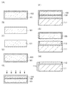
まず、単結晶半導体基板101を準備し、該単結晶半導体基板101を硫酸過酸化水素水
混合溶液(SPM)、アンモニア過酸化水素水混合溶液(APM)、塩酸過酸化水素水混
合溶液(HPM)、希フッ酸(DHF)、オゾン水などを適宜使って洗浄する。単結晶半
導体基板101は、市販の単結晶半導体基板を用いることができ、例えば、単結晶のシリ
コン基板やゲルマニウム基板、ガリウムヒ素やインジウムリン等の化合物半導体基板が挙
げられる。市販のシリコン基板としては、直径5インチ(125mm)、直径6インチ(
150mm)、直径8インチ(200mm)、直径12インチ(300mm)、直径18
インチ(450mm)サイズの円形のものが代表的である。なお、形状は円形に限られず
矩形状等に加工したシリコン基板を用いることも可能である。以下の説明では、単結晶半
導体基板101として、単結晶シリコン基板を用いる場合について説明する。
First, a single
150 mm), diameter 8 inches (200 mm), diameter 12 inches (300 mm),
A circular shape having an inch (450 mm) size is typical. The shape is not limited to a circular shape, and a silicon substrate processed into a rectangular shape or the like can also be used. In the following description, a case where a single crystal silicon substrate is used as the single
次いで、単結晶半導体基板101に熱酸化処理(第1の熱酸化処理とも記す)を行うこと
により酸化膜102(第1の酸化膜とも記す)を形成する(図1(A))。単結晶半導体
基板の製造時や加工の過程で、金属などの不純物が単結晶半導体基板に含まれてしまう場
合がある。そして、当該金属などの不純物は、最終的に形成されるSOI基板に含まれて
しまうおそれがある。そこで、本実施の形態において熱酸化処理は、酸化性雰囲気中にハ
ロゲンを添加した酸化を行うことが好ましい。酸化性雰囲気中にハロゲンを添加するため
のガスとして、HCl、HF、NF3、HBr、Cl2、DCE(dichloroet
hylene)、ClF3、BCl3、F2、Br2などから選ばれた一種又は複数種を
用いることができる。本実施の形態では、酸素に対しHClを0.5〜10体積%(好ま
しくは3体積%)の割合で含む雰囲気中で、900℃〜1150℃の温度(代表的には1
000℃)で熱酸化処理を行うと良い。処理時間は0.1〜6時間、好ましくは0.5〜
1時間とすればよい。形成される酸化膜の膜厚としては、10nm〜1000nm(好ま
しくは50nm〜300nm)、例えば200nmの厚さとする。また、ジクロロエチレ
ンとしてトランス−1,2−ジクロロエチレンを用いる場合は、トランス1,2ジクロロ
エチレンは熱分解する温度が低いため、熱酸化処理の温度を低温で行いたい場合に有効と
なる。なお、トランス−1,2−ジクロロエチレンにかえて、シス−1,2−ジクロロエ
チレン、1,1−ジクロロエチレンや、これらの中から二種類以上のガスの混合ガスを用
いてもよい。
Next, thermal oxidation treatment (also referred to as first thermal oxidation treatment) is performed on the single
hyrene), ClF 3 , BCl 3 , F 2 , Br 2, or the like can be used. In this embodiment mode, a temperature of 900 ° C. to 1150 ° C. (typically 1%) in an atmosphere containing HCl at 0.5 to 10% by volume (preferably 3% by volume) with respect to oxygen.
(000 ° C.). Treatment time is 0.1 to 6 hours, preferably 0.5 to
One hour is sufficient. The thickness of the oxide film to be formed is 10 nm to 1000 nm (preferably 50 nm to 300 nm), for example, 200 nm. In addition, when trans-1,2-dichloroethylene is used as dichloroethylene,
このようにして単結晶半導体基板101の表面に形成された酸化膜102は、酸化性雰囲
気に含まれるハロゲン(例えば、塩素)の作用により、酸化膜102中に金属などの不純
物がゲッタリングされ、単結晶半導体基板101中の金属などの不純物の濃度が低下する
か又は除去される。すなわち、ハロゲンの作用により、金属などの不純物が揮発性のハロ
ゲン化物(例えば、塩化物)となって気相中へ離脱され、単結晶半導体基板101から除
去される。これは、単結晶半導体基板101の表面を化学的機械研磨処理したものに対し
て有効である。さらに、熱酸化処理による酸化膜102の形成を、900℃〜1150℃
の温度範囲で行うため、単結晶半導体基板101の結晶性の改善が行われる。なお、化学
機械研磨(Chemical Mechanical Polishing、略称:CM
P)とは、アルカリ性溶液と研磨砥粒を混合させたスラリーを用いて化学的、かつ、機械
的に研磨して表面を平坦化する処理である。
In this manner, the
Therefore, the crystallinity of the single
P) is a process of flattening the surface by chemical and mechanical polishing using a slurry in which an alkaline solution and abrasive grains are mixed.
次いで、当該金属などの不純物をゲッタリングした酸化膜102を除去する(図1(B)
)。酸化膜102を除去する手法としては、酸化膜102を除去できる手法であれば特に
限定はないが、例えば、バッファーフッ酸、その他フッ酸系のエッチャントを用いて行う
ことができる。当該金属などの不純物をゲッタリングした酸化膜102を除去することに
より、金属などの不純物が低減又は除去された単結晶半導体基板101を得ることができ
る。
Next, the
). The method for removing the
酸化膜102を除去した後、単結晶半導体基板101にレーザ光を照射する(図1(C)
)。単結晶半導体基板101にレーザ光を照射することにより、単結晶半導体基板101
を溶融させることができる。レーザ光の照射による単結晶半導体基板101の溶融は、部
分溶融であることが好ましい。部分溶融状態とは、単結晶半導体基板101の上部が溶融
して液体となるが、下部は溶融せずに固体のままの状態であることをいう。部分溶融状態
とした後に、融液を融点以下の温度にすると、単結晶半導体基板101の溶融されていな
い固相部分(種結晶)と、溶融された液相部分(融液)との界面において、融液側の原子
が種結晶に付着することにより結晶が成長していく。このようにして、結晶成長を進行さ
せることで、単結晶半導体基板101中の結晶欠陥の低減とともに表面凹凸を低減させる
ことができる。
After the
). By irradiating the single
Can be melted. The melting of the single
レーザ光を発振するレーザは、連続発振レーザ、繰り返し周波数が10MHz以上のパル
スレーザ(疑似連続発振レーザ)及びパルス発振レーザのいずれを用いることもできる。
単結晶半導体基板101を部分溶融状態とするには、連続発振レーザまたは疑似発振レー
ザを用いることが好ましい。単結晶半導体基板101の厚さ方向全体へ長時間加熱するこ
とが可能となり、表面にリッジと呼ばれる突起が形成されるのを防止することができる。
例えば、KrFレーザなどのエキシマレーザ、Arレーザ、Krレーザ、CO2レーザ等
の気体レーザがある。その他、固体レーザとして、YAGレーザ、YVO4レーザ、YL
Fレーザ、YAlO3レーザ、GdVO4レーザ、KGWレーザ、KYWレーザ、アレキ
サンドライトレーザ、Ti:サファイアレーザ、Y2O3レーザ等がある。なお、エキシ
マレーザはパルス発振レーザであるが、YAGレーザなどの固体レーザには、連続発振レ
ーザにも、疑似連続発振レーザにも、パルス発振レーザにもなるものがある。
As a laser that oscillates laser light, any of a continuous wave laser, a pulse laser (pseudo continuous wave laser) having a repetition frequency of 10 MHz or more, and a pulsed laser can be used.
In order to bring the single
For example, there is an excimer laser such as a KrF laser, a gas laser such as an Ar laser, a Kr laser, or a CO 2 laser. Other solid-state lasers include YAG laser, YVO 4 laser, YL
There are F laser, YAlO 3 laser, GdVO 4 laser, KGW laser, KYW laser, alexandrite laser, Ti: sapphire laser, Y 2 O 3 laser, and the like. An excimer laser is a pulsed laser, but some solid-state lasers such as a YAG laser can be a continuous wave laser, a pseudo continuous wave laser, or a pulsed laser.
単結晶半導体基板101の結晶欠陥を低減するためのレーザ光の照射強度は、単結晶半導
体基板を部分溶融状態とすることができる程度の強度であることが好ましい。
The irradiation intensity of laser light for reducing crystal defects in the single
レーザ光の照射雰囲気は、希ガス又は窒素雰囲気のような不活性雰囲気、又は真空状態で
行うことが好ましい。窒素などの不活性雰囲気や真空状態の方が、大気雰囲気よりもクラ
ックやリッジの発生を抑える効果が高くなるため、レーザ光の使用可能なエネルギー範囲
を広くすることができる。
The irradiation atmosphere of the laser beam is preferably performed in an inert atmosphere such as a rare gas or a nitrogen atmosphere, or in a vacuum state. An inert atmosphere such as nitrogen or a vacuum state has a higher effect of suppressing the generation of cracks and ridges than the air atmosphere, so that the usable energy range of the laser beam can be widened.
例えば、熱酸化処理を行わずに結晶成長時導入欠陥を低減するためにレーザ光を照射した
場合、単結晶半導体基板101の表面及び内部に存在する金属などの不純物が単結晶半導
体基板101中に拡散するおそれがある。上述したように、金属などの不純物が除去され
た単結晶半導体基板101にレーザ光を照射することにより、単結晶半導体基板101の
結晶欠陥を効率よく低減することができる。また、単結晶半導体基板101に存在してい
る結晶欠陥をあらかじめ低減しておくことによって、後にこの結晶欠陥に起因して発生す
る結晶欠陥を低減することができる。
For example, when laser light is irradiated to reduce defects introduced during crystal growth without performing thermal oxidation treatment, impurities such as metals existing on the surface and inside of the single
ここで、レーザ光の照射により、単結晶半導体基板の表面凹凸及びナノスケールの結晶欠
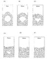
陥が回復する様子を古典分子動力学計算により説明する。具体的には、表面凹凸及びナノ
スケールの結晶欠陥を有する単結晶シリコン基板の上部を加熱して、当該単結晶シリコン
基板を部分溶融させ、下部に残存した固相を種結晶としてシリコン原子が再配列する様子
を示す。なお、本計算においては、単結晶半導体基板101を単結晶シリコン基板とする
。
Here, how the surface irregularities and nanoscale crystal defects of the single crystal semiconductor substrate are recovered by laser light irradiation will be described by classical molecular dynamics calculation. Specifically, the upper part of a single crystal silicon substrate having surface irregularities and nanoscale crystal defects is heated to partially melt the single crystal silicon substrate, and silicon atoms are regenerated using the solid phase remaining in the lower part as a seed crystal. The state of arrangement is shown. Note that in this calculation, the single
古典分子動力学法では、現実の原子の動きに合致する関数(原子間ポテンシャル)を作成
し、当該関数を用いて各原子に働く力を評価し、ニュートンの運動方程式を解くことで、
各原子の運動(時間発展)を追跡することができる。実際の計算手順では、以下のような
サイクルを繰り返すことになる。
(1)計算系の原子に対して、初期座標、初期速度(温度)などの初期条件を与える。
(2)原子間ポテンシャルより原子間力を求める。
(3)時間刻みΔt後の原子の位置、速度を求める。
(4)(2)に戻る。
In classical molecular dynamics, we create a function (interatomic potential) that matches the actual movement of atoms, evaluate the force acting on each atom using the function, and solve Newton's equation of motion.
The movement (time evolution) of each atom can be tracked. In the actual calculation procedure, the following cycle is repeated.
(1) Give initial conditions such as initial coordinates and initial velocity (temperature) to the atoms in the calculation system.
(2) Find the interatomic force from the interatomic potential.
(3) Find the position and velocity of the atom after time step Δt.
(4) Return to (2).
上記手順により、各原子の時間軌跡を求めることができる。なお、上記計算を行うための
古典分子動力学計算ソフトウェアとして、富士通株式会社製のMaterials Ex
plorer5.0を用いた。
The time trajectory of each atom can be obtained by the above procedure. In addition, as a classical molecular dynamics calculation software for performing the above calculation, Materials Ex manufactured by Fujitsu Limited.
plorer 5.0 was used.
シリコンの原子間ポテンシャルとしては、様々なモデルが提唱されているが、本実施例で
は、現状、実験から求まる物性値を最も良く再現できるTersoffポテンシャルを用
いた。なお、Tersoffモデルにおける温度と、現実の温度との間には一定のずれが
存在するが、これは計算上の問題に過ぎないため、融点を基準に現実の温度に換算するこ
とが可能である。シリコンの融点の実験値は約1414℃であり、これは、Tersof
fモデルでは約2327℃にあたる。以下において、現実のシリコンの融点を基準に換算
した温度を、便宜上、換算温度と呼ぶことにする。
Various models have been proposed as the interatomic potential of silicon, but in this example, the Tersoff potential that can best reproduce the physical property values obtained from experiments is used. Note that there is a certain difference between the temperature in the Tersoff model and the actual temperature, but this is only a calculation problem, and can be converted to the actual temperature based on the melting point. . The experimental melting point of silicon is about 1414 ° C., which is
In the f model, it is about 2327 ° C. Hereinafter, the temperature converted based on the actual melting point of silicon will be referred to as a converted temperature for convenience.
次に、単結晶シリコン基板((100)面)の平坦化及び再単結晶化の計算モデルと、そ
の計算条件について説明する。計算に係る単位胞(計算単位胞)のサイズは、x軸方向に
3.26nm、y軸方向に3.26nm、z軸方向に6.52nmとした。ここで、x軸
及びy軸は、単結晶シリコン基板に平行な方向であり、z軸は単結晶シリコン基板の板厚
方向である。なお、計算に当たって、周期境界条件を適用することで、x軸方向及びy軸
方向に十分広い膜を想定することとした。
Next, a calculation model of flattening and re-single crystallization of a single crystal silicon substrate ((100) plane) and calculation conditions thereof will be described. The size of the unit cell for calculation (calculation unit cell) was 3.26 nm in the x-axis direction, 3.26 nm in the y-axis direction, and 6.52 nm in the z-axis direction. Here, the x-axis and the y-axis are directions parallel to the single crystal silicon substrate, and the z-axis is the thickness direction of the single crystal silicon substrate. In the calculation, a sufficiently wide film is assumed in the x-axis direction and the y-axis direction by applying the periodic boundary condition.
計算モデルとしては、表面に凹凸があり、内部にナノスケールの結晶欠陥が存在する単結
晶シリコン基板として、以下の条件のものを採用した。
・単結晶シリコン基板の表面にはピラミッド型の凸部分が存在する。
・凸部分の高さ(単結晶シリコン基板表面の高低差)は1.36nmである。
・座標(1.63、1.63、2.17)を中心として、半径1nm以内の領域に存在す
るシリコン原子(合計191原子)を取り除き、直径約2nmの球状の結晶欠陥を形成す
る。なお、上記の座標の各パラメータは、原点からの距離(nm)に対応している。
・計算単位胞内のシリコン原子の数は、1706個である。
・単結晶シリコン基板の下側7層(合計504原子)は、種結晶とするため、原子の位置
を固定する(固相状態を想定)。
As a calculation model, a single crystal silicon substrate having irregularities on the surface and having nanoscale crystal defects inside was used under the following conditions.
-A pyramidal convex portion exists on the surface of the single crystal silicon substrate.
The height of the convex portion (the difference in height of the single crystal silicon substrate surface) is 1.36 nm.
Centering on coordinates (1.63, 1.63, 2.17), silicon atoms (total 191 atoms) existing in a region within a radius of 1 nm are removed, and spherical crystal defects having a diameter of about 2 nm are formed. In addition, each parameter of said coordinate respond | corresponds to the distance (nm) from an origin.
The number of silicon atoms in the calculation unit cell is 1706.
-Since the lower seven layers (total 504 atoms) of the single crystal silicon substrate are used as seed crystals, the positions of the atoms are fixed (assuming a solid phase state).
yz平面に垂直な方向から見た上記計算モデルの様子を図2(A)に示す。また、上記計
算モデルにおいて、球状の結晶欠陥の中心部を通り、且つ、yz平面に平行な平面におけ
る断面図を図2(B)に示す。なお、図2(B)は、x軸方向に0.65nmの厚みを持
たせて上記計算モデルを示したものであり、厳密には、球状の結晶欠陥の中心部を通る断
面のみを示しているわけではない。
FIG. 2A shows the state of the calculation model viewed from the direction perpendicular to the yz plane. FIG. 2B shows a cross-sectional view in a plane parallel to the yz plane and passing through the center of the spherical crystal defect in the calculation model. FIG. 2B shows the above calculation model with a thickness of 0.65 nm in the x-axis direction. Strictly speaking, only a cross section passing through the center of a spherical crystal defect is shown. I don't mean.
上記の計算モデルを用い、温度の初期条件を換算温度1458℃(融点以上)として、古
典分子動力学計算を行った。なお、本実施の形態においては、初期状態(0sec)から
700psecまでは、温度条件を一定(換算温度1458℃)として計算を行っている
。
Using the above calculation model, classical molecular dynamics calculation was performed with an initial temperature condition of 1458 ° C. (melting point or higher). In this embodiment, the calculation is performed with the temperature condition being constant (converted temperature 1458 ° C.) from the initial state (0 sec) to 700 psec.
単結晶シリコン基板の経時的な構造変化の様子を図3(A)から図3(F)に示す。図3
(A)から図3(F)は、初期状態(0sec)から50psec後までの単結晶シリコ
ン基板の構造変化の様子を、10psec間隔で示している。図3により、50psec
程度で表面の凸部分が融解し、結晶欠陥が消滅し、単結晶シリコン基板が平坦化すること
がわかる。
FIGS. 3A to 3F show the structural changes over time of the single crystal silicon substrate. FIG.
FIGS. 3A to 3F show the structural change of the single crystal silicon substrate from the initial state (0 sec) to 50 psec later at intervals of 10 psec. According to FIG. 3, 50 psec
It can be seen that the convex portion of the surface is melted at a degree, the crystal defects disappear, and the single crystal silicon substrate is flattened.
本計算では、700psec以降、融点以下である換算温度1276℃に引き下げて古典
分子動力学計算を行った。ここでも、700psecから1400psecまでは、温度
条件を一定(1276℃)としている。図4には、700psec以降の単結晶シリコン
基板の経時的な構造変化の様子を示す。図4(A)から図4(C)は、700psecか
ら1400psecまでの単結晶シリコン基板の構造変化の様子を、350psec間隔
で示すものである。
In this calculation, classical molecular dynamics calculation was performed after 700 psec with a reduced temperature of 1276 ° C., which is lower than the melting point. Again, the temperature condition is constant (1276 ° C.) from 700 psec to 1400 psec. FIG. 4 shows a state of structural change over time of a single crystal silicon substrate after 700 psec. 4A to 4C show the state of structural change of a single crystal silicon substrate from 700 psec to 1400 psec at intervals of 350 psec.
図4に示すように、時間経過とともに固液界面が単結晶シリコン基板の表面方向へと上昇
しており、固相部分を種結晶として溶融シリコンが結晶シリコンへと変化することがわか
る。1400psec後には表面付近まで再単結晶化された。
As shown in FIG. 4, the solid-liquid interface rises toward the surface of the single crystal silicon substrate with time, and it can be seen that the molten silicon changes into crystalline silicon using the solid phase portion as a seed crystal. After 1400 psec, it was re-single-crystallized to near the surface.
本計算により、表面凹凸及びナノスケールの結晶欠陥を有する単結晶シリコン基板の上部
を加熱し、溶融させることで、結晶欠陥の消滅と共に表面凹凸が低減する様子が確認され
た。また、下部に残存した固相を種結晶としてシリコン原子が再配列して、結晶成長が進
行する様子が確認された。
This calculation confirmed that the top surface of the single crystal silicon substrate having surface irregularities and nanoscale crystal defects was heated and melted to reduce the surface irregularities as the crystal defects disappeared. In addition, it was confirmed that the silicon atoms rearranged using the solid phase remaining in the lower part as a seed crystal and the crystal growth proceeded.
上記古典分子動力学計算の結果より、直径2nm程度の結晶欠陥及び高低差1.5nm程
度の表面凹凸であれば、溶融時間が50psec程度でも十分に可能であることが分かる
。また、少なくとも700psec程度の溶融時間があれば、下部に残存した固相を種結
晶としてシリコン原子の再配列(再単結晶化)が可能であることが分かる。よって、連続
発振レーザ又は疑似連続発振レーザを用いることにより、十分に欠陥を修復させることが
でき、平坦化処理を行うことができる。また、一般に、パルスレーザ光を用いた場合の半
導体膜の溶融時間は、レーザ光のパルス幅と同程度であるから、パルス幅が50psec
以上であれば、2nm程度の結晶欠陥及び高低差1.5nm程度の表面凹凸を回復させる
ことができると言える。同様に、パルス幅が700psec以上であれば、シリコン原子
の再配列(再単結晶化)が可能であると言える。すなわち、上記の結晶欠陥の低減、表面
凹凸の低減、及びシリコン原子の再配列(再単結晶化)を実現するためには、700ps
ec以上(例えば、25nsec)のパルス幅を有するパルスレーザ光を用いるとよい。
From the results of the classical molecular dynamics calculation, it can be seen that a crystal defect having a diameter of about 2 nm and a surface irregularity having a height difference of about 1.5 nm can be sufficiently achieved even with a melting time of about 50 psec. It can also be seen that if the melting time is at least about 700 psec, the silicon atoms can be rearranged (re-single crystallization) using the solid phase remaining in the lower part as a seed crystal. Therefore, by using a continuous wave laser or a pseudo continuous wave laser, defects can be sufficiently repaired and a planarization process can be performed. In general, when the pulse laser beam is used, the melting time of the semiconductor film is approximately the same as the pulse width of the laser beam, so that the pulse width is 50 psec.
If it is above, it can be said that the crystal | crystallization defect of about 2 nm and the surface unevenness | corrugation of the height difference of about 1.5 nm can be recovered. Similarly, if the pulse width is 700 psec or more, it can be said that rearrangement of silicon atoms (re-single crystallization) is possible. That is, in order to realize the above-described reduction of crystal defects, reduction of surface irregularities, and rearrangement of silicon atoms (re-single crystallization), 700 ps
A pulsed laser beam having a pulse width of ec or more (for example, 25 nsec) may be used.
また、単結晶半導体基板101の表面に所望の平坦性が得られていない場合には、その表
面を平坦化するため、化学的機械研磨(CMP)を行うことが好ましい。単結晶半導体基
板101の平坦性を向上させることにより、後に形成する酸化膜103を平坦に形成する
ことができる。なお、レーザ光の照射により、所望の平坦性が得られるようであれば、平
坦化工程は省略してもかまわない。
In addition, when desired flatness is not obtained on the surface of the single
次いで、単結晶半導体基板101に熱酸化処理(第2の熱酸化処理とも記す)を行うこと
により酸化膜103(第2の酸化膜とも記す)を形成する(図1(D))。第2の熱酸化
処理は、第1の熱酸化処理と同様に行うことができる。形成される酸化膜103の膜厚と
しては、10nm〜1000nm(好ましくは50nm〜300nm)の厚さとする。熱
酸化処理により得られる酸化膜103は、平滑性を有し親水性表面を形成することができ
る。
Next, thermal oxidation treatment (also referred to as second thermal oxidation treatment) is performed on the single
また、ハロゲンを添加して熱酸化処理を行うことにより形成される酸化膜103中にはハ
ロゲンが含まれている。ハロゲンの濃度が、1×10¹⁶/cm3〜5×1021/cm
3の範囲で含まれることにより、金属などの不純物を捕獲して単結晶半導体基板101の
汚染を防止するブロッキング層としての機能を発現させることができる。また、熱酸化処
理に含まれるハロゲンにより単結晶半導体基板101の表面の未結合手が終端されるため
、酸化膜103と単結晶半導体基板101との界面の局在準位密度を低減させることがで
きる。
Further, halogen is contained in the
By being included in the range of 3 , the function as a blocking layer that captures impurities such as metal and prevents contamination of the single
なお、本実施の形態では、塩素原子を含有する酸化膜102及び酸化膜103の形成方法
として、塩化水素やジクロロエチレンを含有させた酸化性雰囲気中で熱酸化処理を行う場
合を示したが、これに限られない。例えば、単結晶半導体基板101に酸化性雰囲気で熱
酸化処理を行い、単結晶半導体基板101表面に酸化膜102(例えば、SiOx)を形
成した後(図1(A)参照)、イオンドーピング装置又はイオン注入装置を用いて、電界
で加速された塩素イオンを添加することにより、酸化膜102中に塩素原子を含有させて
もよい。他にも、表面を塩化水素(HCl)溶液で処理した後に酸化性雰囲気中で熱酸化
処理を行ってもよい。
Note that in this embodiment mode, as a method for forming the
次いで、酸化膜103を介して、単結晶半導体基板101にイオンを照射することにより
、イオンを単結晶半導体基板101に導入し、単結晶半導体基板101の一方の面から所
定の深さの領域に脆化領域104を形成する(図1(E))。
Next, by irradiating the single
脆化領域104が形成される深さは、イオン種、イオンの運動エネルギー、イオンの入射
角によって調節することができる。運動エネルギーは加速電圧などにより調節できる。イ
オンの平均侵入深さとほぼ同じ深さの領域に脆化領域104が形成される。イオンを導入
する深さで、後の工程において単結晶半導体基板101から分離される単結晶半導体層の
厚さが決定される。脆化領域104が形成される深さは10nm以上500nm以下であ
り、好ましい深さの範囲は、50nm以上200nm以下である。
The depth at which the embrittled
イオンを単結晶半導体基板101に導入するには、イオンドーピング装置を用いることが
できる。イオンドーピング装置は、ソースガスを励起しプラズマを生成し、プラズマ中か
らイオンを引き出し、イオンを質量分離せずに被処理物に導入する。イオンドーピング装
置を用いることにより、単結晶半導体基板101に対して均一なドーピングを行うことが
できる。なお、質量分離装置を備えているイオンドーピング装置では、質量分離を伴うイ
オン注入を行うことができる。
In order to introduce ions into the single
イオンドーピング法を用いる場合、イオンの導入の際に用いるソースガスとしては、水素
ガス、希ガス等があるが、本実施の形態では水素ガスを用いることが好ましい。ソースガ
スとして水素ガスを用いた場合、生成されるイオンは、H+、H2 +及びH3 +であるが
、H3 +が最も多く導入されることが好ましい。H3 +は、H+、H2 +よりも導入効率
が良く、導入時間の短縮を図ることができる。また、後の工程において脆化領域104に
亀裂が生じやすくなる。
In the case of using an ion doping method, a source gas used for introduction of ions includes a hydrogen gas, a rare gas, and the like. In this embodiment mode, it is preferable to use a hydrogen gas. When hydrogen gas is used as the source gas, the generated ions are H + , H 2 + and H 3 + , but it is preferable that H 3 + is introduced most often. H 3 + has higher introduction efficiency than H + and H 2 + and can shorten the introduction time. In addition, a crack is easily generated in the embrittled
このようにして、単結晶半導体基板101にイオンを導入することにより、単結晶半導体
基板101には大量の結晶欠陥が形成される。単結晶半導体基板101に結晶成長時に導
入された結晶欠陥や、ウエハの加工時に形成された結晶欠陥が残存していると、これらの
結晶欠陥を起因にして、単結晶半導体基板101に発生する結晶欠陥が増大する。後に、
単結晶半導体層が形成される領域に、これらの結晶欠陥が大量に残存していると、良質な
SOI基板が得られなくなる。本実施の形態に示す方法により、結晶成長時に導入された
結晶欠陥や、ウエハの加工時に形成された結晶欠陥をあらかじめ低減することによって、
イオンの導入の際に形成される結晶欠陥を低減することができる。
In this way, by introducing ions into the single
If a large amount of these crystal defects remain in the region where the single crystal semiconductor layer is formed, a high-quality SOI substrate cannot be obtained. By reducing in advance crystal defects introduced during crystal growth and crystal defects formed during wafer processing by the method shown in this embodiment,
Crystal defects formed during the introduction of ions can be reduced.
また、イオンドーピング法を用いる場合、イオンドーピング装置は質量分離を行わずイオ
ンを導入するため、水素イオンの他に金属イオンも同時に単結晶半導体基板101へ導入
される場合がある。金属イオンは質量数が大きいので、イオンが導入される側の最表面に
多く分布する。本実施の形態では単結晶半導体基板101の表面に酸化膜103が形成さ
れている。この酸化膜103の膜厚を金属イオンの導入される深さよりも厚く形成するこ
とで、当該金属の分布を酸化膜103中に止めておくことができる。酸化膜103にハロ
ゲンを含ませることにより、重金属など単結晶半導体基板101に悪影響を与える不純物
をゲッタリングする作用がある。それにより酸化膜103中に捕集した当該不純物を固定
して単結晶半導体基板101の汚染を防ぐことができる。
In the case of using the ion doping method, the ion doping apparatus introduces ions without performing mass separation, and thus metal ions in addition to hydrogen ions may be introduced into the single
次いで、単結晶半導体基板101と貼り合わせるための半導体基板111を準備する。半
導体基板111は、単結晶半導体基板101として用いる基板と同様の基板を用いること
ができる。さらには、多結晶半導体基板、太陽電池の製造に用いられる太陽電池級シリコ
ン基板(SOG−Si:Solar grade Silicon、例えばSi純度が9
9.9999%のもの)等も用いることができる。本明細書に示す多結晶半導体基板とは
、多結晶シリコン基板に加え、多結晶化合物半導体基板も含み、さらには微量にゲルマニ
ウムを含む多結晶シリコン基板、微量にボロンを含む多結晶シリコン基板を指すものとす
る。
Next, a
9.9999%) can also be used. The polycrystalline semiconductor substrate shown in this specification includes a polycrystalline compound semiconductor substrate in addition to a polycrystalline silicon substrate, a polycrystalline silicon substrate containing a small amount of germanium, and a polycrystalline silicon substrate containing a small amount of boron. Shall.
また、半導体基板111と酸化膜103との接着を良好に行うために、接合面を活性化し
ておいてもよい。例えば、接着する面の一方又は双方に原子ビーム若しくはイオンビーム
を照射する。原子ビーム若しくはイオンビームを利用する場合には、アルゴン等の不活性
ガス中性原子ビーム若しくは不活性ガスイオンビームを用いることができる。その他に、
プラズマ照射若しくはラジカル処理を行うことで接合面を活性化することもできる。この
よう活性化処理により、400℃以下の温度であっても単結晶半導体基板と半導体基板と
の接合をすることが容易となる。
Further, the bonding surface may be activated in order to satisfactorily bond the
The bonding surface can also be activated by performing plasma irradiation or radical treatment. Such activation treatment makes it easy to bond the single crystal semiconductor substrate and the semiconductor substrate even at a temperature of 400 ° C. or lower.
次いで、酸化膜103と半導体基板111の一方の面とが向かい合うようにボンディング
(接着)する(図1(F))。酸化膜103と半導体基板111とを密着させることによ
り、ファン・デル・ワールス力で基板同士が引き合う。そして、基板の表面にできたSi
−OH同士が水素結合で接着する。低温(例えば、150℃〜200℃)の熱処理により
脱水縮合反応が起こり、水分子が離脱してシリコン原子間に酸素原子を介した結合(Si
−O−Si)ができる。さらに高温で熱処理(例えば600℃)を行うことにより、酸素
が拡散し界面はSi同士が結合し、単結晶半導体基板101と半導体基板111との接着
がより強固なものとなる。本実施の形態において、単結晶半導体基板101と半導体基板
111とを接着させるための絶縁膜として、熱酸化処理により得られる酸化膜103を用
いている。熱酸化処理により得られる酸化膜103は平滑性を有しているため、単結晶半
導体基板101と半導体基板111との接着を良好に行うことができる。
Next, bonding is performed so that the
-OH bonds with each other through hydrogen bonds. A dehydration condensation reaction occurs by heat treatment at a low temperature (for example, 150 ° C. to 200 ° C.), water molecules are detached, and bonds between silicon atoms via oxygen atoms (Si
-O-Si). Further, by performing heat treatment at a high temperature (for example, 600 ° C.), oxygen diffuses and Si is bonded to each other at the interface, whereby adhesion between the single
なお、単結晶半導体基板101と半導体基板111を接着させる前に、単結晶半導体基板
101上に形成された酸化膜103及び半導体基板111の表面処理を行うことが好まし
い。表面処理としては、オゾン処理(例えば、オゾン水洗浄)、又はメガソニック洗浄及
びオゾン水洗浄を行うことができる。また、オゾン水洗浄とフッ酸による洗浄を複数回繰
り返し行ってもよい。このような表面処理を行うことにより、酸化膜103及び半導体基
板111の表面の有機物等のゴミを除去し、酸化膜103の表面を親水性にすることがで
きる。
Note that before the single
単結晶半導体基板101と半導体基板111とを貼り合わせた後は、加熱処理を加圧処理
の一方又は両方を行うことが好ましい。加熱処理や加圧処理を行うことにより単結晶半導
体基板101と半導体基板111との接着強度を向上させることが可能である。加熱処理
は、脆化領域104に導入した原子又は分子が析出しない温度とし、その加熱温度は35
0℃以下が好ましい。言い換えれば、この加熱温度は脆化領域104からガスが抜けない
温度である。加圧処理は、接着面に対して垂直な方向に圧力が加わるように行い、単結晶
半導体基板101及び半導体基板111の耐圧性を考慮して行う。
After the single
0 ° C. or lower is preferable. In other words, this heating temperature is a temperature at which gas does not escape from the embrittled
単結晶半導体基板101に熱処理を行うことにより、前記脆化領域104において前記単
結晶半導体基板101を分割して、単結晶半導体層112が接着された半導体基板111
と単結晶半導体基板105とに分離する(図1(G))。ここでの加熱処理には、RTA
(Rapid Thermal Anneal)装置、ハロゲンランプ若しくは赤外線ラ
ンプで加熱するRTA(LRTA;Lamp Rapid Thermal Annea
l)装置を用いることができる。この加熱処理で、単結晶半導体層112が接着された半
導体基板111の温度が、550℃以上650℃以下の範囲となるように上昇させること
が好ましい。
By performing heat treatment on the single
And the single crystal semiconductor substrate 105 (FIG. 1G). For the heat treatment here, RTA
(Rapid Thermal Anneal) RTA (LRTA; Lamp Rapid Thermal Annea) heated with a device, halogen lamp or infrared lamp
l) An apparatus can be used. Through this heat treatment, the temperature of the
本実施の形態では、抵抗加熱を有する縦型炉を用いた加熱処理を行う。単結晶半導体基板
101が貼りつけられた半導体基板111を縦型炉のボートに載置する。ボートを縦型炉
のチャンバーに搬入する。単結晶半導体基板101の酸化を抑制するため、まずチャンバ
ー内を排気して真空状態とする。真空度は、5×10⁻³Pa程度とする。真空状態にし
た後、窒素をチャンバー内に供給して、チャンバー内を窒素雰囲気にする。この間、温度
を200℃に上昇させる。
In this embodiment mode, heat treatment using a vertical furnace having resistance heating is performed. The
チャンバー内を窒素雰囲気にした後、温度200℃で2時間加熱する。その後、1時間か
けて400℃に温度上昇させる。加熱温度400℃の状態が安定したら、1時間かけて6
00℃に温度上昇させる。加熱温度600℃の状態が安定したら、600℃で2時間加熱
処理する。その後、1時間かけて400℃まで下げ、10分〜30分間後に、チャンバー
内からボートを搬出する。大気雰囲気中で、ボート上の単結晶半導体基板101、及び単
結晶半導体基板101が接着された半導体基板111を冷却する。
After making the inside of a chamber into nitrogen atmosphere, it heats at the temperature of 200 degreeC for 2 hours. Thereafter, the temperature is raised to 400 ° C. over 1 hour. When the heating temperature is stable at 400 ° C, 6
Increase the temperature to 00 ° C. When the state of the heating temperature of 600 ° C. is stabilized, heat treatment is performed at 600 ° C. for 2 hours. Thereafter, the temperature is lowered to 400 ° C. over 1 hour, and after 10 to 30 minutes, the boat is carried out of the chamber. In an air atmosphere, the single
上記の抵抗加熱炉を用いた加熱処理は、単結晶半導体基板101と半導体基板111との
結合力を強化するための加熱処理と、脆化領域104に分離を生じさせる加熱処理が連続
して行われる。この2つの加熱処理を異なる装置で行う場合は、例えば、抵抗加熱炉にお
いて、処理温度200℃、処理時間2時間の加熱処理を行った後、貼り合わされた半導体
基板111と単結晶半導体基板101を炉から搬出する。次いで、RTA装置で、処理温
度600℃以上700℃以下、処理時間1分以上30分以下の加熱処理を行い、単結晶半
導体基板101を脆化領域104で分割させる。
In the heat treatment using the resistance heating furnace, the heat treatment for strengthening the bonding force between the single
このように、熱処理を行い脆化領域104において分割(劈開)することにより、半導体
基板111上に、酸化膜103を介して単結晶半導体層112を設けることができる(図
1(G))。
In this manner, the single
半導体基板111に接着された単結晶半導体層112中及び表面には、脆化領域104の
形成及び脆化領域104による分離によるダメージが残存しており、結晶性や平坦性が損
なわれている。そこで、得られた単結晶半導体層112に対して平坦化処理を行うことが
好ましい(図1(H))。平坦化処理を行うことにより、単結晶半導体層112中及び表
面の結晶欠陥を低減し、結晶性を回復させ、単結晶半導体層112の表面を平坦化させる
ことができる。また、平坦化処理を行うことにより、単結晶半導体層112を薄膜化させ
ることができる。
Damage due to formation of the embrittled
平坦化処理としては、CMP、エッチング処理、レーザ光の照射のいずれか一方又は複数
の方法を組み合わせて行うことができる。例えば、ドライエッチング又はウェットエッチ
ングの一方、又は双方を組み合わせたエッチング処理(エッチバック処理)を行った後に
レーザ光を照射するとよい。
As the planarization treatment, any one of CMP, etching treatment, laser light irradiation, or a combination of a plurality of methods can be performed. For example, laser light may be irradiated after an etching process (etchback process) in which one of dry etching or wet etching or a combination of both is performed.
ドライエッチング処理では、エッチングガスとして、塩化硼素、塩化珪素または四塩化炭
素などの塩化物ガス、塩素ガス、弗化硫黄、弗化窒素などの弗化物ガス、酸素ガスなどを
用いることができる。ウェットエッチング処理では、エッチング液として、例えば、水酸
化テトラメチルアンモニウム(tetramethylammonium hydrox
ide、略称;TMAH)溶液等を用いることができる。エッチング処理を行うことによ
り、単結晶半導体層112の表面に存在する分離によるダメージを除去することができる
。また、レーザ光を照射する前に、単結晶半導体層112の表面に存在するダメージを除
去しておくことにより、レーザ光を照射して単結晶半導体層112が溶融した際に、ダメ
ージを単結晶半導体層中に取り込むことを防止することができる。
In the dry etching process, as an etching gas, a chloride gas such as boron chloride, silicon chloride, or carbon tetrachloride, a fluoride gas such as chlorine gas, sulfur fluoride, or nitrogen fluoride, or an oxygen gas can be used. In the wet etching process, for example, tetramethylammonium hydroxide (tetramethylammonium hydroxide) is used as an etchant.
ide, abbreviation: TMAH) solution or the like can be used. By performing the etching treatment, damage due to separation existing on the surface of the single
レーザ光を単結晶半導体層112の上面側から照射することで、単結晶半導体層112の
上面を溶融させることができる。溶融した後、単結晶半導体層112が冷却、固化するこ
とによって、上面の平坦性が向上した単結晶半導体層112が得られる。レーザ光を用い
ることにより、半導体基板111が直接加熱されないため、該半導体基板111の温度上
昇を抑えることができる。
By irradiation with laser light from the upper surface side of the single
なお、単結晶半導体層の欠陥を低減するためのパルスレーザの照射強度は、パルスレーザ
の照射による単結晶半導体層の溶融状態が、部分溶融状態、又は部分溶融状態と完全溶融
状態の境界付近の状態(以下、「初期の完全溶融状態」と呼ぶ。)となるようにすること
が好ましい。「初期の完全溶融状態」以外の完全溶融状態とする場合には、液体となった
後の無秩序な核発生により微結晶化し、結晶性が低下する可能性が高いためである。ここ
で、部分溶融状態とは、この場合、単結晶半導体層の上部は溶融して液体となるが、下部
は溶融せずに固体のままであることをいう。他方、完全溶融状態とは、単結晶半導体層が
下部絶縁層との界面まで溶融され、液体状態になることをいう。
Note that the irradiation intensity of the pulse laser for reducing defects in the single crystal semiconductor layer is such that the melting state of the single crystal semiconductor layer by the pulse laser irradiation is in the partially molten state or in the vicinity of the boundary between the partially molten state and the completely molten state. It is preferable to be in a state (hereinafter referred to as “initial complete melting state”). This is because in the case of a completely melted state other than the “initial fully melted state”, there is a high possibility that the crystallinity is lowered due to disordered nucleation after becoming a liquid and crystallinity is lowered. Here, the partially molten state means that in this case, the upper part of the single crystal semiconductor layer is melted to become a liquid, but the lower part is not melted and remains solid. On the other hand, the completely melted state means that the single crystal semiconductor layer is melted to the interface with the lower insulating layer to be in a liquid state.
一方で、部分溶融状態とする場合には、溶融されていない固体の領域から結晶成長が進行
するため、結晶性を保ったまま欠陥を低減することができる。また、「初期の完全溶融状
態」とする場合には、下方への熱の拡散により、単結晶半導体層と下部絶縁層との界面付
近から固化し、これを種結晶として、再度の単結晶化を進行させることができる。「初期
の完全溶融状態」においては、原子の配列が完全にランダムになっているわけではなく、
特に、温度上昇が小さい下部絶縁層との界面付近においては、原子配列は固体状態の単結
晶半導体層のものと相違がない。このため、下部絶縁層との界面付近からの固化により、
結晶性を低下させることなく欠陥を低減することができるものと考えられる。または、下
部絶縁層との界面付近において、溶融していない固体が僅かに残存しており、これを種結
晶として結晶成長が進行している可能性もある。
On the other hand, in the case of a partially melted state, crystal growth proceeds from an unmelted solid region, so that defects can be reduced while maintaining crystallinity. In addition, in the case of an “initial complete melting state”, by the diffusion of heat downward, it is solidified from the vicinity of the interface between the single crystal semiconductor layer and the lower insulating layer, and this is used as a seed crystal for re-single crystallisation. Can be advanced. In the "initial fully molten state", the arrangement of atoms is not completely random,
In particular, in the vicinity of the interface with the lower insulating layer where the temperature rise is small, the atomic arrangement is no different from that of the solid single crystal semiconductor layer. For this reason, by solidification from the vicinity of the interface with the lower insulating layer,
It is considered that defects can be reduced without reducing crystallinity. Alternatively, there is a possibility that a little unmelted solid remains in the vicinity of the interface with the lower insulating layer, and crystal growth is progressing using this as a seed crystal.
上記レーザ光の照射には、パルス発振レーザを用いることが好ましい。これは瞬間的に高
エネルギーのパルスレーザ光を発振することができ、溶融状態を作り出すことが容易とな
るためである。発振周波数は、1Hz以上10MHz以下程度とすることが好ましい。
A pulsed laser is preferably used for the laser light irradiation. This is because high-energy pulsed laser light can be instantaneously oscillated, and it becomes easy to create a molten state. The oscillation frequency is preferably about 1 Hz to 10 MHz.
このようにして、平坦化処理を行うことにより、単結晶半導体層中の結晶欠陥を低減し、
結晶性を回復させ、単結晶半導体層の表面を平坦化させることができる。なお、本実施の
形態において、単結晶半導体層表面のダメージを除去する際に、エッチング処理を用いた
場合について説明したが、本発明の一態様はこれに限られず、CMPを用いることもでき
る。
In this way, by performing planarization treatment, crystal defects in the single crystal semiconductor layer are reduced,
Crystallinity can be recovered and the surface of the single crystal semiconductor layer can be planarized. Note that although the case where etching treatment is used to remove damage on the surface of the single crystal semiconductor layer is described in this embodiment, one embodiment of the present invention is not limited to this, and CMP can also be used.
なお、平坦化処理を行った後に、単結晶半導体層112の膜厚を小さくする薄膜化工程を
行ってもよい。単結晶半導体層112の薄膜化処理には、ドライエッチング又はウェット
エッチングの一方、又は双方を組み合わせたエッチング処理(エッチバック処理)を適用
すればよい。例えば、単結晶半導体層112がシリコン材料からなる層である場合、ドラ
イエッチングとしてSF6とO2をプロセスガスに用いて、単結晶半導体層112を薄く
することができ、所望の単結晶半導体層112の膜厚を得ることができる。このとき得ら
れる単結晶半導体層112の膜厚は、例えば、10nm〜150nm、好ましくは10n
m〜50nmとする。なお、平坦化処理を行った後に所望の単結晶半導体層112の膜厚
が得られるようであれば、薄膜化処理を行わなくてもかまわない。
Note that after the planarization treatment, a thinning process for reducing the thickness of the single
m to 50 nm. Note that as long as a desired film thickness of the single
以上の工程により、半導体基板111上に酸化膜103を介して単結晶半導体層112が
設けられたSOI基板113を作製することができる。本実施の形態で示した作製方法を
用いることによって、単結晶半導体基板101に含まれる金属などの不純物を除去した後
に、単結晶半導体基板101にレーザ光を照射することにより、単結晶半導体基板101
に存在する結晶成長時に導入された結晶欠陥やウエハ加工時に形成された結晶欠陥を効率
良く低減することができる。また、単結晶半導体基板101に存在している結晶欠陥をあ
らかじめ低減しておくことによって、その後の工程において発生する結晶欠陥を低減する
ことができる。さらに、単結晶半導体基板101の分割後に、単結晶半導体層112中及
び表面に対して平坦化処理を行うことにより、単結晶半導体層112中及び表面の結晶欠
陥を低減し、結晶性を回復させ、表面を平坦化することができる。その結果、単結晶半導
体層112の結晶欠陥が低減され、結晶性に優れたSOI基板を作製することができる。
Through the above steps, an
It is possible to efficiently reduce crystal defects introduced during crystal growth and crystal defects formed during wafer processing. In addition, by reducing crystal defects existing in the single
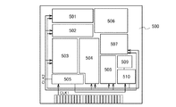
また本実施の形態は図1に示した構成に限られず、例えば、図5乃至図7に示す構成とし
てもよい。図5に、半導体基板111上に絶縁膜106と酸化膜103を介して単結晶半
導体層112を設けた構成を示す。絶縁膜106は、半導体基板111上に、酸化珪素、
酸化窒化珪素、窒化珪素、窒化酸化珪素等の酸化性を有する材料を用いて形成する。絶縁
膜106は、上記の材料を用いた単数の膜を用いたものであっても、複数の膜を積層して
用いたものであってもよい。
Further, the present embodiment is not limited to the configuration shown in FIG. 1, and for example, the configuration shown in FIGS. FIG. 5 illustrates a structure in which the single
It is formed using an oxidizing material such as silicon oxynitride, silicon nitride, or silicon nitride oxide. The insulating
例えば、酸化珪素を絶縁膜106として用いる場合、絶縁膜106はシランと酸素、TE
OS(テトラエトキシシラン)と酸素等の混合ガスを用い、熱CVD、プラズマCVD、
常圧CVD、バイアスECRCVD等の気相成長法によって形成することができる。絶縁
膜106の膜厚は、10nm〜1000nm(好ましくは50nm〜300nm)の厚さ
とすることができる。この場合、絶縁膜106の表面を酸素プラズマ処理で緻密化しても
よい。また、窒化珪素を絶縁膜106として用いる場合、シランとアンモニアの混合ガス
を用い、プラズマCVD法等の気相成長法によって形成することができる。また、窒化酸
化珪素膜を絶縁膜106として用いる場合、シランとアンモニアの混合ガス、又はシラン
と酸化窒素の混合ガスを用いてプラズマCVD等の気相成長法によって形成することがで
きる。
For example, when silicon oxide is used as the insulating
Using a mixed gas such as OS (tetraethoxysilane) and oxygen, thermal CVD, plasma CVD,
It can be formed by vapor phase growth methods such as atmospheric pressure CVD and bias ECRCVD. The thickness of the insulating
また絶縁膜106として、有機シランガスを用いて化学気相成長法により作製される酸化
珪素を用いていても良い。有機シランガスとしては、珪酸エチル(TEOS:化学式Si
(OC2H5)4)、テトラメチルシラン(TMS:化学式Si(CH3)4)、テトラ
メチルシクロテトラシロキサン(TMCTS)、オクタメチルシクロテトラシロキサン(
OMCTS)、ヘキサメチルジシラザン(HMDS)、トリエトキシシラン(SiH(O
C2H5)3)、トリスジメチルアミノシラン(SiH(N(CH3)2)3)等のシリ
コン含有化合物を用いることができる。
As the insulating
(OC 2 H 5 ) 4 ), tetramethylsilane (TMS: chemical formula Si (CH 3 ) 4 ), tetramethylcyclotetrasiloxane (TMCTS), octamethylcyclotetrasiloxane (
OMCTS), hexamethyldisilazane (HMDS), triethoxysilane (SiH (O
Silicon-containing compounds such as C 2 H 5 ) 3 ) and trisdimethylaminosilane (SiH (N (CH 3 ) 2 ) 3 ) can be used.
なお、本明細書において、酸化窒化物とは、その組成として、窒素原子よりも酸素原子の
数が多い物質とし、また、窒化酸化物とは、その組成として、酸素原子より窒素原子の数
が多い物質とする。なお、酸化窒化シリコン膜とは、その組成として、窒素よりも酸素の
含有量が多いものであって、ラザフォード後方散乱法(RBS:Rutherford
Backscattering Spectrometry)及び水素前方散乱法(HF
S:Hydrogen Forward Scattering)を用いて測定した場合
に、濃度範囲として酸素が50〜70原子%、窒素が0.5〜15原子%、Siが25〜
35原子%、水素が0.1〜10原子%の範囲で含まれるものをいう。また、窒化酸化シ
リコン膜とは、その組成として、酸素よりも窒素の含有量が多いものであって、RBS及
びHFSを用いて測定した場合に、濃度範囲として酸素が5〜30原子%、窒素が20〜
55原子%、Siが25〜35原子%、水素が10〜30原子%の範囲で含まれるものを
いう。但し、酸化窒化シリコンまたは窒化酸化シリコンを構成する原子の合計を100原
子%としたとき、窒素、酸素、Si及び水素の含有比率が上記の範囲内に含まれるものと
する。
Note that in this specification, oxynitride is a substance having a larger number of oxygen atoms than nitrogen atoms, and nitride oxide is a composition having a number of nitrogen atoms greater than oxygen atoms. Use many substances. Note that the silicon oxynitride film has a composition that contains more oxygen than nitrogen, and has a Rutherford backscattering method (RBS: Rutherford).
Backscattering Spectrometry) and hydrogen forward scattering (HF)
When measured using S (Hydrogen Forward Scattering), the concentration ranges from 50 to 70 atomic% for oxygen, 0.5 to 15 atomic% for nitrogen, and 25 to 25 for Si.
35 atomic% and hydrogen are contained in the range of 0.1 to 10 atomic%. In addition, the silicon nitride oxide film has a composition containing more nitrogen than oxygen. When measured using RBS and HFS, the concentration range of oxygen is 5 to 30 atomic%, nitrogen. 20 ~
55 atomic%, Si is 25 to 35 atomic%, and hydrogen is included in the range of 10 to 30 atomic%. However, when the total number of atoms constituting silicon oxynitride or silicon nitride oxide is 100 atomic%, the content ratio of nitrogen, oxygen, Si, and hydrogen is included in the above range.
半導体基板111上に絶縁膜106を形成した後に、表面に酸化膜103が形成され、表
面から所定の深さの領域に脆化領域104が形成された単結晶半導体基板101(図1(
A)乃至(E)参照)と半導体基板111とを絶縁膜106を介して接着する。次に、熱
処理を行い脆化領域104において分割することにより、半導体基板111上に絶縁膜1
06及び酸化膜103を介して単結晶半導体層112を形成することができる。なお、該
単結晶半導体層112に対して平坦化処理を行ってもよい。これらの方法は、図1(F)
乃至(H)において示した方法を用いればよいため、詳しい説明を省略する。
After the insulating
A) to (E)) and the
A single
Since the method shown in (H) to (H) may be used, detailed description is omitted.
以上により、図5に示すSOI基板を作製することができる。なお、絶縁膜106を半導
体基板111側に設ける例を示したが、本発明の一態様はこれに限定されず、単結晶半導
体基板101側に設けることもできる。その場合は、単結晶半導体基板101の表面に形
成されている酸化膜103上に形成することができる。
Through the above steps, the SOI substrate illustrated in FIG. 5 can be manufactured. Note that although the example in which the insulating
熱酸化処理により得られる酸化膜は平滑性を有しているため、該酸化膜上に絶縁膜106
を形成した場合は、絶縁膜106の平滑性も向上させることができる。よって、単結晶半
導体基板と半導体基板との接着を良好に行うことができる。また、半導体基板111側に
絶縁膜106を形成した場合は、半導体基板111の表面に凹凸があったとしても、平坦
化する膜として機能させることができる。よって、単結晶半導体基板と半導体基板との接
着を良好に行うことができる。
Since the oxide film obtained by the thermal oxidation treatment has smoothness, the insulating
In the case where is formed, the smoothness of the insulating
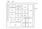
図6に、半導体基板111上に酸化膜114と酸化膜103を介して単結晶半導体層11
2を設けた構成を示す。酸化膜114は、酸化膜103と同様にして、半導体基板111
に熱酸化処理を行うことにより形成することができる。熱酸化処理はドライ酸化で行って
も良いが、酸化性雰囲気中にハロゲンを添加した酸化を行うことが好ましい。酸化性雰囲
気中にハロゲンを添加するためのガスとして、HCl、HF、NF3、HBr、Cl2、
DCE(Dichloroethylene)、ClF3、BCl3、F2、Br2など
から選ばれた一種又は複数種を用いることができる。形成される酸化膜114の膜厚とし
ては、10nm〜1000nm(好ましくは50nm〜300nm)とする。
In FIG. 6, the single crystal semiconductor layer 11 is formed over the
The structure which provided 2 is shown. The
It can be formed by performing a thermal oxidation treatment. The thermal oxidation treatment may be performed by dry oxidation, but it is preferable to perform oxidation with halogen added in an oxidizing atmosphere. As gases for adding halogen to the oxidizing atmosphere, HCl, HF, NF 3 , HBr, Cl 2 ,
One or a plurality of types selected from DCE (Dichloroethylene), ClF 3 , BCl 3 , F 2 , Br 2 and the like can be used. The thickness of the
このようにして半導体基板111の表面に形成された酸化膜114は、酸化性雰囲気に含
まれるハロゲンの作用により、酸化膜114中に金属などの不純物がゲッタリングされ、
半導体基板111中の金属などの不純物の濃度が低下するか又は除去される。すなわち、
ハロゲンの作用により、金属などの不純物が揮発性の塩化物となって気相中へ離脱され、
単結晶半導体基板101から除去される。これは、単結晶半導体基板101の表面をCM
Pしたものに対して有効である。さらに、熱酸化処理による酸化膜114の形成を900
℃〜1150℃の温度範囲で行うため、単結晶半導体基板101の結晶性の改善を行うこ
とができる。
Thus, the
The concentration of impurities such as metal in the
Due to the action of halogens, impurities such as metals become volatile chlorides and are released into the gas phase,
The single
Effective for P Further, the formation of the
Since it is performed in a temperature range of from 1 to 150 ° C., the crystallinity of the single
半導体基板111の表面に酸化膜114を形成した後に、表面に酸化膜103が形成され
、表面から所定の深さの領域に脆化領域104が形成された単結晶半導体基板101(図
1(A)乃至(E)参照)と半導体基板111とを酸化膜114及び酸化膜103を介し
て接着する。次に、熱処理を行い脆化領域104において分割することにより、半導体基
板111上に酸化膜114及び酸化膜103を介して単結晶半導体層112を形成するこ
とができる。なお、該単結晶半導体層112に対して平坦化処理を行ってもよい。これら
の方法は、図1(F)乃至(H)において示した方法を用いればよいため、詳しい説明を
省略する。以上により、図6に示すSOI基板を作製することができる。
After the
単結晶半導体基板101及び半導体基板111の表面に熱酸化処理による酸化膜を形成す
ることによって、半導体基板111から単結晶半導体層112へ不純物が拡散し、単結晶
半導体層112が汚染することを防ぐブロッキング層として機能する。また、熱酸化処理
により得られる酸化膜は平滑性を有しているため、単結晶半導体基板と半導体基板との接
着を良好に行うことができる。
By forming an oxide film by thermal oxidation treatment on the surfaces of the single
図7に、半導体基板111上に酸化膜114、絶縁膜106及び酸化膜103を介して単
結晶半導体層112を設けた構成を示す。酸化膜114及び絶縁膜106は、上記に示し
た方法で形成することができる。なお、絶縁膜106は、単結晶半導体基板101及び半
導体基板111のどちらか一方又は両方に設けることができる。
FIG. 7 illustrates a structure in which the single
半導体基板111に酸化膜114を形成し、該酸化膜114上に絶縁膜106を形成した
後に、図1(D)と同様にして酸化膜103が形成されて、脆化領域104が形成された
単結晶半導体基板101と貼り合わせる。図1(G)、(H)と同様の工程を行うことに
より、図7に示すSOI基板を作製することができる。
After the
単結晶半導体基板101及び半導体基板111の表面に熱酸化処理による酸化膜を形成し
、さらに絶縁膜106を形成することによって、半導体基板111から単結晶半導体層1
12へ不純物が拡散し、単結晶半導体層112が汚染することを防ぐブロッキング層とし
て機能する。また、熱酸化処理により得られる酸化膜は平滑性を有しているため、該酸化
膜上に絶縁膜106を形成することによって、絶縁膜106の平滑性も向上させることが
できる。よって、単結晶半導体基板と半導体基板との接着を良好に行うことができる。
By forming an oxide film by thermal oxidation treatment on the surfaces of the single
12 functions as a blocking layer that prevents impurities from diffusing into the single
本実施の形態では、塩素原子を含有する酸化膜114の形成方法として、塩化水素やジク
ロロエチレンを含有させた酸化性雰囲気中で熱酸化処理を行う場合を示したが、これに限
られない。例えば、半導体基板111に酸化性雰囲気で熱酸化処理を行い、半導体基板1
11表面に酸化膜114(例えば、SiOx)を形成した後、イオンドーピング装置又は
イオン注入装置を用いて、電界で加速された塩素イオンを添加することにより酸化膜11
4中に塩素原子を含有させてもよい。他にも、表面を塩化水素(HCl)溶液で処理した
後に酸化性雰囲気中で熱酸化処理を行ってもよい。
In this embodiment, the case where the thermal oxidation treatment is performed in an oxidizing atmosphere containing hydrogen chloride or dichloroethylene is shown as a method for forming the
After an oxide film 114 (for example, SiOx) is formed on the surface of the oxide film 11, an oxide film 11 is added by adding chlorine ions accelerated by an electric field using an ion doping apparatus or an ion implantation apparatus.
4 may contain a chlorine atom. In addition, after the surface is treated with a hydrogen chloride (HCl) solution, thermal oxidation treatment may be performed in an oxidizing atmosphere.
本実施の形態は、他の実施の形態と自由に組み合わせて行うことができる。 This embodiment can be freely combined with any of the other embodiments.
以下において、本発明の特徴の一であるイオンの照射方法について考察する。 Hereinafter, an ion irradiation method which is one of the features of the present invention will be considered.
本発明の一態様では、水素(H)に由来するイオン(以下「水素イオン種」と呼ぶ)を単
結晶半導体基板に対して照射している。より具体的には、水素ガス又は水素を組成に含む
ガスを原材料として用い、水素プラズマを発生させ、該水素プラズマ中の水素イオン種を
単結晶半導体基板に対して照射している。
In one embodiment of the present invention, a single crystal semiconductor substrate is irradiated with ions derived from hydrogen (H) (hereinafter referred to as “hydrogen ion species”). More specifically, hydrogen plasma or a gas containing hydrogen in its composition is used as a raw material, hydrogen plasma is generated, and a single crystal semiconductor substrate is irradiated with hydrogen ion species in the hydrogen plasma.
(水素プラズマ中のイオン)
上記のような水素プラズマ中には、H+、H2 +、H3 +といった水素イオン種が存在す
る。ここで、各水素イオン種の反応過程(生成過程、消滅過程)について、以下に反応式
を列挙する。
e+H→e+H++e ・・・・・(1)
e+H2→e+H2 ++e ・・・・・(2)
e+H2→e+(H2)*→e+H+H ・・・・・(3)
e+H2 +→e+(H2 +)*→e+H++H ・・・・・(4)
H2 ++H2→H3 ++H ・・・・・(5)
H2 ++H2→H++H+H2 ・・・・・(6)
e+H3 +→e+H++H+H ・・・・・(7)
e+H3 +→H2+H ・・・・・(8)
e+H3 +→H+H+H ・・・・・(9)
(Ions in hydrogen plasma)
Hydrogen ion species such as H + , H 2 + , and H 3 + exist in the hydrogen plasma as described above. Here, the reaction formulas are listed below for the reaction process (generation process, annihilation process) of each hydrogen ion species.
e + H → e + H + + e (1)
e + H 2 → e + H 2 + + e (2)
e + H 2 → e + (H 2 ) * → e + H + H (3)
e + H 2 + → e + (H 2 + ) * → e + H + + H (4)
H 2 + + H 2 → H 3 + + H (5)
H 2 + + H 2 → H + + H + H 2 (6)
e + H 3 + → e + H + + H + H (7)
e + H 3 + → H 2 + H (8)
e + H 3 + → H + H + H (9)
図8に、上記の反応の一部を模式的に表したエネルギーダイアグラムを示す。なお、図8
に示すエネルギーダイアグラムは模式図に過ぎず、反応に係るエネルギーの関係を厳密に
規定するものではない点に留意されたい。なお、以下の反応式は、実験的に観測されてい
ないため、図8では、バツ印で示している。
H2+H+→H3 + ・・・・・ (10)
H2 ++H→H3 + ・・・・・ (11)
FIG. 8 shows an energy diagram schematically showing a part of the above reaction. Note that FIG.
It should be noted that the energy diagram shown in Fig. 1 is only a schematic diagram and does not strictly define the energy relationship related to the reaction. In addition, since the following reaction formula is not observed experimentally, in FIG. 8, it is shown by the cross mark.
H 2 + H + → H 3 + (10)
H 2 + + H → H 3 + (11)
(H3 +の生成過程)
上記のように、H3 +は、主として反応式(5)により表される反応過程により生成され
る。一方で、反応式(5)と競合する反応として、反応式(6)により表される反応過程
が存在する。H3 +が増加するためには、少なくとも、反応式(5)の反応が、反応式(
6)の反応より多く起こる必要がある(なお、H3 +が減少する反応としては他にも(7
)、(8)、(9)が存在するため、(5)の反応が(6)の反応より多いからといって
、必ずしもH3 +が増加するとは限らない。)。反対に、反応式(5)の反応が、反応式
(6)の反応より少ない場合には、プラズマ中におけるH3 +の割合は減少する。
(H 3 + generation process)
As described above, H 3 + is produced mainly by the reaction process represented by the reaction formula (5). On the other hand, as a reaction competing with the reaction formula (5), there is a reaction process represented by the reaction formula (6). In order to increase H 3 + , at least the reaction of the reaction formula (5)
It is necessary to occur more than the reaction of (6) (in addition, there are other reactions that reduce H 3 + (7
), (8), and (9) exist, and just because the reaction of (5) is more than the reaction of (6), H 3 + does not necessarily increase. ). On the other hand, when the reaction of the reaction formula (5) is less than the reaction of the reaction formula (6), the ratio of H 3 + in the plasma decreases.
上記反応式における右辺(最右辺)の生成物の増加量は、反応式の左辺(最左辺)で示す
原料の密度や、その反応に係る速度係数などに依存している。ここで、H2 +の運動エネ
ルギーが約11eVより小さい場合には(5)の反応が主要となり(すなわち、反応式(
5)に係る速度係数が、反応式(6)に係る速度係数と比較して十分に大きくなり)、H
2 +の運動エネルギーが約11eVより大きい場合には(6)の反応が主要となることが
実験的に確認されている。
The increase amount of the product on the right side (rightmost side) in the above reaction formula depends on the density of the raw material indicated on the left side (leftmost side) of the reaction formula, the rate coefficient related to the reaction, and the like. Here, when the kinetic energy of H 2 + is smaller than about 11 eV, the reaction of (5) becomes the main (that is, the reaction formula (
The rate coefficient according to 5) is sufficiently larger than the rate coefficient according to reaction equation (6)), H
If 2 + kinetic energy is greater than about 11eV to be a major reaction of (6) has been confirmed experimentally.
荷電粒子は電場から力を受けて運動エネルギーを得る。該運動エネルギーは、電場による
ポテンシャルエネルギーの減少量に対応している。例えば、ある荷電粒子が他の粒子と衝
突するまでの間に得る運動エネルギーは、その間に通過した電位差分のポテンシャルエネ
ルギーに等しい。つまり、電場中において、他の粒子と衝突することなく長い距離を移動
できる状況では、そうではない状況と比較して、荷電粒子の運動エネルギー(の平均)は
大きくなる傾向にある。このような、荷電粒子に係る運動エネルギーの増大傾向は、粒子
の平均自由行程が大きい状況、すなわち、圧力が低い状況で生じ得る。
A charged particle receives a force from an electric field and obtains kinetic energy. The kinetic energy corresponds to a decrease in potential energy due to an electric field. For example, the kinetic energy obtained until a certain charged particle collides with another particle is equal to the potential energy of the potential difference that has passed during that time. That is, in a situation where a long distance can be moved without colliding with other particles in an electric field, the kinetic energy (average) of charged particles tends to be larger than in situations where this is not the case. Such a tendency of increasing the kinetic energy related to the charged particles may occur in a situation where the mean free path of the particles is large, that is, a situation where the pressure is low.
また、平均自由行程が小さくとも、その間に大きな運動エネルギーを得ることができる状
況であれば、荷電粒子の運動エネルギーは大きくなる。すなわち、平均自由行程が小さく
とも、電位差が大きい状況であれば、荷電粒子の持つ運動エネルギーは大きくなると言え
る。
In addition, even if the mean free path is small, the kinetic energy of the charged particles is large if a large kinetic energy can be obtained during that time. That is, even if the mean free path is small, it can be said that the kinetic energy of the charged particles increases if the potential difference is large.
これをH2 +に適用してみる。プラズマの生成に係るチャンバー内のように電場の存在を
前提とすれば、該チャンバー内の圧力が低い状況ではH2 +の運動エネルギーは大きくな
り、該チャンバー内の圧力が高い状況ではH2 +の運動エネルギーは小さくなる。つまり
、チャンバー内の圧力が低い状況では(6)の反応が主要となるため、H3 +は減少する
傾向となり、チャンバー内の圧力が高い状況では(5)の反応が主要となるため、H3 +
は増加する傾向となる。また、プラズマ生成領域における電場(又は電界)が強い状況、
すなわち、ある二点間の電位差が大きい状況ではH2 +の運動エネルギーは大きくなり、
反対の状況では、H2 +の運動エネルギーは小さくなる。つまり、電場が強い状況では(
6)の反応が主要となるためH3 +は減少する傾向となり、電場が弱い状況では(5)の
反応が主要となるため、H3 +は増加する傾向となる。
Let's apply this to H 2 + . Assuming the presence of an electric field as in the chamber related to plasma generation, the kinetic energy of H 2 + increases in a situation where the pressure in the chamber is low, and H 2 + in a situation where the pressure in the chamber is high. The kinetic energy of becomes smaller. That is, since the reaction (6) is dominant in the situation where the pressure in the chamber is low, H 3 + tends to decrease, and in the situation where the pressure in the chamber is high, the reaction (5) is dominant. 3 +
Tends to increase. In addition, the situation where the electric field (or electric field) is strong in the plasma generation region,
That is, in a situation where the potential difference between two points is large, the kinetic energy of H 2 + becomes large,
In the opposite situation, the kinetic energy of H 2 + is small. In other words, in a situation where the electric field is strong (
Since the reaction of 6) is the main, H 3 + tends to decrease, and in the situation where the electric field is weak, the reaction of (5) is the main, so H 3 + tends to increase.
(イオン源による差異)
ここで、イオン種の割合(特にH3 +の割合)が異なる例を示す。図9は、100%水素
ガス(イオン源の圧力:4.7×10⁻²Pa)から生成されるイオンの質量分析結果を
示すグラフである。なお、上記質量分析は、イオン源から引き出されたイオンを測定する
ことにより行った。横軸はイオンの質量である。スペクトル中、質量1、2、3のピーク
は、それぞれ、H+、H2 +、H3 +に対応する。縦軸は、スペクトルの強度であり、イ
オンの数に対応する。図9では、質量が異なるイオンの数量を、質量3のイオンを100
とした場合の相対比で表している。図9から、上記イオン源により生成されるイオンの割
合は、H+:H2 +:H3 +=1:1:8程度となることが分かる。なお、このような割
合のイオンは、プラズマを生成するプラズマソース部(イオン源)と、当該プラズマから
イオンビームを引き出すための引出電極などから構成されるイオンドーピング装置によっ
ても得ることが出来る。
(Difference due to ion source)
Here, an example in which the ratio of ionic species (particularly, the ratio of H 3 + ) is different will be described. FIG. 9 is a graph showing the results of mass spectrometry of ions generated from 100% hydrogen gas (ion source pressure: 4.7 × 10 −2 Pa). In addition, the said mass spectrometry was performed by measuring the ion withdraw | derived from the ion source. The horizontal axis is the mass of ions. In the spectrum, peaks with
This is expressed as a relative ratio. FIG. 9 shows that the ratio of ions generated by the ion source is about H + : H 2 + : H 3 + = 1: 1: 8. Such a ratio of ions can also be obtained by an ion doping apparatus including a plasma source unit (ion source) that generates plasma and an extraction electrode for extracting an ion beam from the plasma.
図10は、図9とは異なるイオン源を用いた場合であって、イオン源の圧力がおおよそ3
×10−3Paの時に、PH3から生成したイオンの質量分析結果を示すグラフである。
上記質量分析結果は、水素イオン種に着目したものである。また、質量分析は、イオン源
から引き出されたイオンを測定することにより行った。図10は、図9と同様、横軸はイ
オンの質量を示し、質量1、2、3のピークは、それぞれH+、H2 +、H3 +に対応す
る。縦軸はイオンの数量に対応するスペクトルの強度である。図10から、プラズマ中の
イオンの割合はH+:H2 +:H3 +=37:56:7程度であることが分かる。なお、
図10はソースガスがPH3の場合のデータであるが、ソースガスとして100%水素ガ
スを用いたときも、水素イオン種の割合は同程度になる。
FIG. 10 shows a case where an ion source different from that shown in FIG.
× When the 10 -3 Pa, which is a graph showing the results of mass spectrometry of ions generated from PH 3.
The mass spectrometry results are focused on hydrogen ion species. Further, mass spectrometry was performed by measuring ions extracted from the ion source. In FIG. 10, as in FIG. 9, the horizontal axis indicates the mass of ions, and the peaks of
FIG. 10 shows data when the source gas is PH 3 , but when 100% hydrogen gas is used as the source gas, the ratio of the hydrogen ion species is about the same.
図10のデータを得たイオン源の場合には、H+、H2 +及びH3 +のうち、H3 +が7
%程度しか生成されていない。他方、図9のデータを得たイオン源の場合には、H3 +の
割合を50%以上(上記の条件では80%程度)とすることが可能である。これは、上記
考察において明らかになったチャンバー内の圧力及び電場に起因するものと考えられる。
In the case of the ion source from which the data of FIG. 10 is obtained, H 3 + is 7 among H + , H 2 + and H 3 +.
Only about% is generated. On the other hand, in the case of the ion source that has obtained the data of FIG. 9, the ratio of H 3 + can be set to 50% or more (about 80% under the above conditions). This is considered to be caused by the pressure and electric field in the chamber, which has been clarified in the above consideration.
(H3 +の照射メカニズム)
図9のような複数のイオン種を含むプラズマを生成し、生成されたイオン種を質量分離し
ないで単結晶半導体基板に照射する場合、単結晶半導体基板の表面には、H+、H2 +、
H3 +の各イオンが照射される。イオンの照射からイオン導入領域形成にかけてのメカニ
ズムを再現するために、以下の5種類のモデルを考える。
1.照射されるイオン種がH+で、照射後もH+(H)である場合。
2.照射されるイオン種がH2 +で、照射後もH2 +(H2)のままである場合。
3.照射されるイオン種がH2 +で、照射後に2個のH(H+)に分裂する場合。
4.照射されるイオン種がH3 +で、照射後もH3 +(H3)のままである場合。
5.照射されるイオン種がH3 +で、照射後に3個のH(H+)に分裂する場合。
(H 3 + irradiation mechanism)
In the case of generating plasma including a plurality of ion species as shown in FIG. 9 and irradiating the single crystal semiconductor substrate without mass separation of the generated ion species, the surface of the single crystal semiconductor substrate has H + , H 2 + ,
Each ion of H 3 + is irradiated. In order to reproduce the mechanism from ion irradiation to ion introduction region formation, the following five types of models are considered.
1. The ion species to be irradiated is H + and is H + (H) after irradiation.
2. The ion species to be irradiated is H 2 + and remains H 2 + (H 2 ) after irradiation.
3. When the ion species to be irradiated is H 2 + and splits into two H (H + ) after irradiation.
4). When the ion species to be irradiated is H 3 + and remains H 3 + (H 3 ) after irradiation.
5. When the ion species to be irradiated is H 3 + and splits into three H (H + ) after irradiation.
(シミュレーション結果と実測値との比較)
上記のモデルを基にして、水素イオン種をSi基板に照射する場合のシミュレーションを
行った。シミュレーション用のソフトウェアとしては、SRIM(the Stoppi
ng and Range of Ions in Matter:モンテカルロ法によ
るイオン導入過程のシミュレーションソフトウェア、TRIM(the Transpo
rt of Ions in Matter)の改良版)を用いている。なお、計算の関
係上、モデル2ではH2 +を質量2倍のH+に置き換えて計算した。また、モデル4では
H3 +を質量3倍のH+に置き換えて計算した。さらに、モデル3ではH2 +を運動エネ
ルギー1/2のH+に置き換え、モデル5ではH3 +を運動エネルギー1/3のH+に置
き換えて計算を行った。
(Comparison between simulation results and measured values)
Based on the above model, a simulation was performed when the Si substrate was irradiated with hydrogen ion species. As simulation software, SRIM (the Stoppi)
ng and Range of Ions in Matter: Monte Carlo simulation software for ion introduction process, TRIM (the Transpo)
rt of Ions in Matter)). Note that, for the calculation, was calculated by replacing the
なお、SRIMは非晶質構造を対象とするソフトウェアではあるが、高エネルギー、高ド
ーズの条件で水素イオン種を照射する場合には、SRIMを適用可能である。水素イオン
種とSi原子の衝突により、Si基板の結晶構造が非単結晶構造に変化するためである。
Note that SRIM is software for an amorphous structure, but SRIM can be applied when irradiating the hydrogen ion species with high energy and high dose. This is because the crystal structure of the Si substrate changes to a non-single crystal structure due to collision between the hydrogen ion species and Si atoms.
図11に、モデル1乃至モデル5を用いて水素イオン種をSi基板に照射した場合(H換
算で10万個照射時)のSi基板中の水素原子数の計算結果を示す。また、図9の水素イ
オン種を照射したSi基板中の水素濃度(SIMS(Secondary Ion Ma
ss Spectroscopy)のデータ)をあわせて示す。モデル1乃至モデル5を
用いて行った計算の結果については、縦軸を水素原子の数で表しており(右軸)、SIM
Sデータについては、縦軸を水素原子の密度で表している(左軸)。横軸はSi基板表面
からの深さである。実測値であるSIMSデータと、計算結果とを比較した場合、モデル
2及びモデル4は明らかにSIMSデータのピークから外れており、また、SIMSデー
タ中にはモデル3に対応するピークも見られない。このことから、モデル2乃至モデル4
の寄与は、相対的に小さいことが分かる。イオンの運動エネルギーが数keV程度である
のに対して、H−Hの結合エネルギーは数eV程度に過ぎないことを考えれば、モデル2
及びモデル4の寄与が小さいのは、Si原子との衝突により、大部分のH2 +やH3 +が
、H+やHに分離しているためと思われる。
FIG. 11 shows the calculation results of the number of hydrogen atoms in the Si substrate when
ss Spectroscopy data) is also shown. About the result of the calculation performed using the
For S data, the vertical axis represents the density of hydrogen atoms (left axis). The horizontal axis is the depth from the surface of the Si substrate. When the SIMS data that is the actual measurement value and the calculation result are compared, the
It can be seen that the contribution of is relatively small. Considering that the kinetic energy of ions is about several keV, whereas the bond energy of HH is only about several eV,
The reason why the contribution of
以上より、モデル2乃至モデル4については、以下では考慮しない。図12乃至図14に
、モデル1及びモデル5を用いて水素イオン種を照射した場合(H換算で10万個照射時
)の計算結果を示す。また、図9の水素イオン種を照射したSi基板中の水素濃度(SI
MSデータ)及び、上記シミュレーション結果をSIMSデータにフィッティングさせた
もの(以下フィッティング関数と呼ぶ)を合わせて示す。ここで、図12は加速電圧を8
0kVとした場合を示し、図13は加速電圧を60kVとした場合を示し、図14は加速
電圧を40kVとした場合を示している。なお、モデル1及びモデル5を用いて行った計
算の結果については、縦軸を水素原子の数で表しており(右軸)、SIMSデータ及びフ
ィッティング関数については、縦軸を水素原子の密度で表している(左軸)。横軸はSi
基板表面からの深さである。
From the above,
MS data) and the result of fitting the simulation result to SIMS data (hereinafter referred to as a fitting function) are also shown. Here, FIG. 12 shows an acceleration voltage of 8
FIG. 13 shows the case where the acceleration voltage is 60 kV, and FIG. 14 shows the case where the acceleration voltage is 40 kV. In addition, about the result of the calculation performed using the
It is the depth from the substrate surface.
フィッティング関数はモデル1及びモデル5を考慮して以下の計算式により求めることと
した。なお、計算式中、X、Yはフィッティングに係るパラメータであり、Vは体積であ
る。
[フィッティング関数]
=X/V×[モデル1のデータ]+Y/V×[モデル5のデータ]
The fitting function is determined by the following calculation formula in consideration of
[Fitting function]
= X / V × [
現実に照射されるイオン種の割合(H+:H2 +:H3 +=1:1:8程度)を考えれば
H2 +の寄与(すなわち、モデル3)についても考慮すべきであるが、以下に示す理由に
より、ここでは除外して考えた。
・モデル3に示される照射過程により導入される水素は、モデル5の照射過程と比較して
僅かであるため、除外して考えても大きな影響はない(SIMSデータにおいても、ピー
クが現れていない)。
・モデル5とピーク位置の近いモデル3は、モデル5において生じるチャネリング(結晶
の格子構造に起因する原子の移動)により隠れてしまう可能性が高い。
すなわち、モデル3のフィッティングパラメータを見積もるのは困難である。これは、本
シミュレーションが非晶質Siを前提としており、結晶性に起因する影響を考慮していな
いことによるものである。
Considering the ratio of ion species actually irradiated (H + : H 2 + : H 3 + = 1: 1: 8 or so), the contribution of H 2 + (that is, model 3) should be considered. For the reasons shown below, it was excluded here.
・ Hydrogen introduced by the irradiation process shown in
The
That is, it is difficult to estimate the fitting parameter of
図15に、上記のフィッティングパラメータをまとめる。いずれの加速電圧においても、
導入されるHの数の比は、[モデル1]:[モデル5]=1:42〜1:45程度(モデ
ル1におけるHの数を1とした場合、モデル5におけるHの数は42以上45以下程度)
であり、照射されるイオン種の数の比は、[H+(モデル1)]:[H3 +(モデル5)
]=1:14〜1:15程度(モデル1におけるH+の数を1とした場合、モデル5にお
けるH3 +の数は14以上15以下程度)である。モデル3を考慮していないことや非晶
質Siと仮定して計算していることなどを考えれば、実際の照射に係るイオン種の比(H
+:H2 +:H3 +=1:1:8程度)に近い値が得られていると言える。
FIG. 15 summarizes the above fitting parameters. At any acceleration voltage
The ratio of the number of H to be introduced is about [Model 1]: [Model 5] = 1: 42 to 1:45 (when the number of H in
The ratio of the number of ion species to be irradiated is [H + (model 1)]: [H 3 + (model 5).
] = 1: 14 to 1:15 (when the number of H + in
It can be said that a value close to + : H 2 + : H 3 + = 1: 1: 8 is obtained.
(H3 +を用いる効果)
図9に示すようなH3 +の割合を高めた水素イオン種を基板に照射することで、H3 +に
起因する複数のメリットを享受することができる。例えば、H3 +はH+やHなどに分離
して基板内に導入されるため、主にH+やH2 +を照射する場合と比較して、イオンの導
入効率を向上させることができる。これにより、半導体基板の生産性向上を図ることがで
きる。また、同様に、H3 +が分離した後のH+やHの運動エネルギーは小さくなる傾向
にあるから、薄い半導体層の製造に向いている。
(Effect of using H 3 + )
By irradiating the substrate with a hydrogen ion species with an increased H 3 + ratio as shown in FIG. 9, a plurality of merits resulting from H 3 + can be obtained. For example, since H 3 + is separated into H + and H and introduced into the substrate, ion introduction efficiency can be improved as compared with the case of mainly irradiating H + and H 2 +. . Thereby, productivity improvement of a semiconductor substrate can be aimed at. Similarly, since the kinetic energy of H + and H after the separation of H 3 + tends to be small, it is suitable for manufacturing a thin semiconductor layer.
なお、本明細書では、H3 +を効率的に照射するために、図9に示すような水素イオン種
を照射可能なイオンドーピング装置を用いる方法について説明している。イオンドーピン
グ装置は廉価で、大面積処理に優れているため、このようなイオンドーピング装置を用い
てH3 +を照射することで、半導体特性の向上、大面積化、低コスト化、生産性向上など
の顕著な効果を得ることができる。一方で、H3 +の照射を第一に考えるのであれば、イ
オンドーピング装置を用いることに限定して解釈する必要はない。
Note that in this specification, a method is described in which an ion doping apparatus that can irradiate hydrogen ion species as illustrated in FIG. 9 is used in order to efficiently perform irradiation with H 3 + . Since the ion doping apparatus is inexpensive and excellent in large area processing, irradiation with H 3 + using such an ion doping apparatus improves the semiconductor characteristics, increases the area, reduces the cost, and improves the productivity. A remarkable effect such as can be obtained. On the other hand, if the irradiation with H 3 + is considered first, there is no need to interpret it limited to using an ion doping apparatus.
(実施の形態2)
本実施の形態では、上記実施の形態と異なるSOI基板の作製方法に関して図面を参照し
て説明する。具体的には、角(端部)に丸みを帯びている(エッジロールオフ(ERO)
を有する)単結晶半導体基板を用いる場合について説明する。また、単結晶半導体基板を
繰り返し利用する(再利用)する場合に関して図面を参照して説明する。なお、本実施の
形態において、上記実施の形態と同様の部分には同じ符号を付し、詳しい説明を省略する
。
(Embodiment 2)
In this embodiment, a method for manufacturing an SOI substrate, which is different from that in the above embodiment, will be described with reference to drawings. Specifically, the corners (edges) are rounded (edge roll-off (ERO)
A case of using a single crystal semiconductor substrate having the above will be described. A case where a single crystal semiconductor substrate is repeatedly used (reused) is described with reference to drawings. Note that in this embodiment, the same parts as those in the above embodiment are denoted by the same reference numerals, and detailed description thereof is omitted.
まず、表面に酸化膜103が設けられ、表面から所定の深さの領域に脆化領域104が形
成された単結晶半導体基板101(ここでは、単結晶シリコン基板)を準備する(図16
(A)参照)。図16(A)については、上述した図1(A)乃至(E)において示した
方法を用いればよいため、詳しい説明を省略する。
First, a single crystal semiconductor substrate 101 (here, a single crystal silicon substrate) in which an
(See (A)). As for FIG. 16A, since the method shown in FIGS. 1A to 1E described above may be used, detailed description is omitted.
本実施の形態では、図16(A)に示すように、単結晶半導体基板101の角(端部)は
丸みを帯びているため、当該端部の表面に酸化膜103が形成される。
In this embodiment mode, as illustrated in FIG. 16A, since the corner (end portion) of the single
次いで、半導体基板111を準備し(図16(B))、酸化膜103と半導体基板111
の一方の面とが向かい合うようにボンディング(接着)する(図16(C))。
Next, the
Bonding (adhesion) is performed so that one of the two surfaces faces each other (FIG. 16C).
次いで、加熱処理を行い脆化領域104にて分離することにより、半導体基板111上に
酸化膜103を介して単結晶半導体層112を形成する(図16(D))。
Next, heat treatment is performed and separation at the embrittled
以上の工程により、半導体基板111上に酸化膜103を介して単結晶半導体層112を
形成することができる(図16(E))。なお、単結晶半導体層112の表面に凹凸があ
る場合には、当該SOI基板を用いてデバイスを形成する前に表面の平坦化処理を行うこ
とが好ましい。平坦化処理は、上記図1(H)で示したようにCMP、エッチング処理、
レーザ光の照射のいずれか一又は複数の方法を組み合わせて行うことができる。平坦化処
理を行うことにより、単結晶半導体層112中及び表面の結晶欠陥を低減し、単結晶半導
体層の結晶性を回復させることができる。
Through the above steps, the single
Any one or a plurality of methods of laser light irradiation can be performed in combination. By performing the planarization treatment, crystal defects in and on the single
図16(A)乃至図16(E)については、上述した実施の形態1において示した方法を
用いれば良いため、詳しい説明を省略する。
A detailed description of FIGS. 16A to 16E is omitted because the method described in
次いで、分離された単結晶半導体基板105を繰り返し利用する工程(半導体基板再生処
理)について説明する。
Next, a process of repeatedly using the separated single crystal semiconductor substrate 105 (semiconductor substrate recycling process) will be described.
単結晶半導体基板101は、エッジロールオフの影響により、単結晶半導体基板101の
端部において半導体基板111との貼り合わせが十分に行われない場合がある。その結果
、端部において単結晶半導体基板105は脆化領域104にて分離されず、酸化膜103
等が残存する場合がある(図16(F))。
In some cases, the single
Etc. may remain (FIG. 16F).
そこで、単結晶半導体基板105の端部における残渣部107を除去する(図16(G)
)。残渣部107は、ウェットエッチング処理を行うことにより除去することができる。
具体的には、フッ化水素酸とフッ化アンモニウムと界面活性剤を含む混合溶液(例えば、
ステラケミファ社製、商品名:LAL500)をエッチャントとして用いてウェットエッ
チングを行う。
Therefore, the
). The
Specifically, a mixed solution containing hydrofluoric acid, ammonium fluoride, and a surfactant (for example,
Wet etching is performed using Stella Chemifa Co., Ltd. (trade name: LAL500) as an etchant.
また、水素イオンが導入された脆化領域104は、TMAH(Tetra Methyl
Ammonium Hydroxide、テトラメチルアンモニウムヒドロキシド)に
代表される有機アルカリ性水溶液を用いてウェットエッチングすることにより、除去する
ことができる。このような処理を行うことにより、単結晶半導体基板105の端部におけ
る残渣物による段差が緩和される。
Further, the
It can be removed by wet etching using an organic alkaline aqueous solution represented by (Ammonium Hydroxide, tetramethylammonium hydroxide). By performing such treatment, a step due to a residue at the end portion of the single
次いで、単結晶半導体基板105をハロゲン雰囲気中で酸化することにより、酸化膜10
8を形成し(図16(H))、その後当該酸化膜108を除去する。ハロゲンとしてはH
Clを用いることができる。このように熱酸化処理により酸化膜108を形成した後、当
該酸化膜108の除去を行うことによって、ハロゲン元素によるゲッタリング効果を得る
ことができる。ゲッタリング効果としては、SOI基板作製時に導入された金属などの不
純物を除去する効果が得られる。すなわち、塩素の作用により、金属などの不純物が揮発
性の塩化物となって気相中へ離脱して除去される。
Next, by oxidizing the single
8 is formed (FIG. 16H), and then the
Cl can be used. Thus, after forming the
次いで、単結晶半導体基板に平坦化処理を行う。平坦化処理としては、CMP、ドライエ
ッチング処理、またはウェットエッチング処理、レーザ光の照射、のいずれか一、又は複
数の方法を組み合わせて行うことができる。本実施の形態では、単結晶半導体基板105
にレーザ光の照射を行う(図16(I))。単結晶半導体基板105にレーザ光を照射す
ることにより、単結晶半導体基板105を溶融させることができる。単結晶半導体基板1
05は、レーザ光によって溶融された部分が冷却し、固化するため、平坦性が向上される
。また、レーザの照射により平坦性の向上とともに、単結晶半導体基板105の結晶欠陥
が減少し、単結晶半導体基板105の結晶性を向上させることができる(図16(J))
。
Next, planarization treatment is performed on the single crystal semiconductor substrate. As the planarization treatment, any one of CMP, dry etching treatment, wet etching treatment, laser light irradiation, or a combination of a plurality of methods can be performed. In this embodiment, the single
Is irradiated with laser light (FIG. 16I). By irradiating the single
In 05, since the portion melted by the laser beam is cooled and solidified, the flatness is improved. Further, flatness is improved by laser irradiation, crystal defects in the single
.
単結晶半導体基板105にレーザ光を照射する具体的な方法は、図1(C)と同様にして
行うことができるため説明を省略する。但し、単結晶半導体基板105に、単結晶半導体
層の分離と再生処理を繰り返し行うことにより、単結晶半導体基板105の厚みは徐々に
薄くなっていく。そこで、図16(I)に示すレーザ光照射工程において、単結晶半導体
基板の厚みに最適な波長、つまり単結晶半導体基板への光の侵入長が単結晶半導体基板の
板厚と同程度の波長を有するCWレーザ光に適宜変更する。波長可変のレーザを用いると
、単結晶半導体基板の膜厚が徐々に薄くなっていっても、一台のレーザで単結晶半導体基
板の板厚に対応できるため効率が良い。このように、単結晶半導体基板の板厚に適宜使用
するCWレーザ光の波長を変更し、レーザ光の照射を行うことで、単結晶半導体基板を最
大限再利用することができる。
A specific method for irradiating the single
単結晶半導体基板105にレーザ光を照射しても、単結晶半導体基板105の端部におい
て、単結晶半導体層112の分離による段差が残っている場合がある。その場合には、レ
ーザ光を照射した後に、CMPにより平坦化することが好ましい。その結果、単結晶半導
体基板105の端部における段差を除去し、単結晶半導体基板105の表面を平坦にする
ことができる。なお、レーザ光の照射により、所望の平坦性が得られるようであれば、平
坦化工程は省略してもかまわない。
Even when the single
以上の工程により、結晶欠陥が低減され、結晶性の高い単結晶半導体基板105を得るこ
とができる。再生処理が行われた単結晶半導体基板105を用いてSOI基板を作製する
際には、図1(D)の工程から作製することができる。
Through the above steps, crystal defects are reduced and the single
このような再生処理を行うことにより、単結晶半導体基板105を用いてSOI基板を作
製した場合であっても、結晶欠陥が低減されたSOI基板を作製することができる。また
、単結晶半導体基板の再生処理工程により単結晶半導体基板を繰り返し利用することによ
って、低コスト化を図ることができる。また、本実施の形態で示した単結晶半導体基板の
再生面を十分に平坦化することができるため、単結晶半導体基板と半導体基板との密着性
を向上させ、貼り合わせ不良を低減することができる。
By performing such regeneration treatment, an SOI substrate with reduced crystal defects can be manufactured even when an SOI substrate is manufactured using the single
本実施の形態は、他の実施の形態と自由に組み合わせて行うことができる。 This embodiment can be freely combined with any of the other embodiments.
(実施の形態3)
本実施の形態では、実施の形態1又は実施の形態2で作製したSOI基板を用いた半導体
装置の作製方法について説明する。ここでは、半導体装置としてCMOS構造を作製する
一例を、図17を用いて説明する。なお、本実施の形態において、上記実施の形態と同様
の部分には同じ符号を付し、詳しい説明を省略する。
(Embodiment 3)
In this embodiment, a method for manufacturing a semiconductor device using the SOI substrate manufactured in
実施の形態1によれば、SOI基板の単結晶半導体層112の厚さを100nm又はそれ
以下とすることができる。単結晶半導体層112の厚さを100nm又はそれ以下とする
と、トランジスタのチャネル形成領域の空乏層の最大深さより薄くなり、顕著なトランジ
スタの電気特性をもたらす。トランジスタのチャネル領域の十分な空乏層化により良好な
S値、しきい値電圧などを得ることができる。さらに、CMOS構造を作製した場合、早
いスイッチング速度を得ることができる。
According to
まず、実施の形態1に従ってSOI基板を得た後、単結晶半導体層112上に素子分離絶
縁層を形成するためのマスクとなる保護層206を形成する。この段階の工程断面図が図
17(A)に相当する。保護層206は酸化シリコン膜や窒化シリコン膜などを用いる。
First, after an SOI substrate is obtained according to
なお、しきい値電圧を制御するために、硼素、アルミニウム、ガリウムなどのp型不純物
を単結晶半導体層112に添加しておくことが好ましい。例えば、p型不純物として硼素
を5×1017cm−3以上1×1018cm−3以下の濃度で添加されていてもよい。
Note that a p-type impurity such as boron, aluminum, or gallium is preferably added to the single
次いで、保護層206をマスクとしてエッチングを行い、露呈している単結晶半導体層1
12及びその下方の酸化膜103の一部を除去する。次いで、TEOSを用いて酸化シリ
コン膜を化学気相成長法で堆積する。この酸化シリコン膜は、単結晶半導体層112が埋
め込まれるように厚く堆積する。次いで、単結晶半導体層112に重なる酸化シリコン膜
を研磨により除去した後、保護層206を除去して、素子分離絶縁層207を残存させる
。この段階の工程断面図が図17(B)に相当する。
Next, etching is performed using the
12 and a portion of the
次いで、第1の絶縁膜を形成し、第1の絶縁膜上に導電材料を含むポリシリコン膜を有す
るゲート電極209を形成し、ゲート電極209をマスクとして第1の絶縁膜をエッチン
グしてゲート絶縁層208を形成する。ゲート絶縁層208は、PECVD法又はスパッ
タリング法等を用いて得られる酸化珪素、窒化酸化珪素、窒化珪素、酸化ハフニウム、酸
化アルミニウム又は酸化タンタルを含む膜の単層、又はこれらの積層である。ゲート絶縁
層208は、PECVD法を行うことにより単結晶半導体層112の表面を覆って薄い膜
厚、例えば20nmの膜厚で形成することができる。また、高密度プラズマ処理により単
結晶半導体層112の表面を酸化又は窒化することで形成してもよい。高密度プラズマ処
理は、例えばHe、Ar、Kr、Xeなどの希ガス、酸素、酸化窒素、アンモニア、窒素
、水素などの混合ガスとを用いて行う。この場合プラズマの励起をマイクロ波により行う
ことで、低電子温度で高密度のプラズマを生成することができる。このような高密度のプ
ラズマで生成された酸素ラジカル(OHラジカルを含む場合もある)や窒素ラジカル(N
Hラジカルを含む場合もある)によって、単結晶半導体層112の表面を酸化又は窒化す
ることにより、1〜50nm、望ましくは5〜30nmの絶縁膜が単結晶半導体層112
に接するように形成される。実施の形態1に示すように、平坦化処理を行うことにより、
単結晶半導体層の表面が十分に平坦化されるため、厚さ20nmの絶縁膜をゲート絶縁層
208として用いても、十分なゲート耐圧を得ることができる。この段階の工程断面図が
図17(C)に相当する。
Next, a first insulating film is formed, a
In some cases, the surface of the single
It is formed so as to be in contact with. As shown in
Since the surface of the single crystal semiconductor layer is sufficiently planarized, a sufficient gate breakdown voltage can be obtained even when an insulating film with a thickness of 20 nm is used as the
次いで、ゲート電極209を覆う第2の絶縁膜210を形成し、nFETとなる領域にA
sなどをドーピングして浅い接合深さの第1不純物領域211を形成し、pFETとなる
領域にBなどをドーピングして浅い接合深さの第2の不純物領域212を形成する。さら
に、サイドウォール絶縁層213、214を形成する。pFETとなる領域のサイドウォ
ール絶縁層214は、nFETとなる領域のサイドウォール絶縁層213よりも幅を広く
する。この段階の工程断面図が図17(C)に相当する。
Next, a second
A
次いで、第2の絶縁膜210を部分的にエッチングしてゲート電極209の上面と、第1
不純物領域211及び第2不純物領域212とを露出させる。次いで、nFETとなる領
域にAsなどをドーピングして深い接合深さの第3不純物領域215を形成し、pFET
なる領域にBなどをドーピングして深い接合深さの第4不純物領域216を形成する。次
いで、活性化のための熱処理(800℃〜1100℃)を行う。次いで、シリサイドを形
成するための金属膜としてコバルト膜を成膜する。次いで、RTAなどの熱処理(500
℃、1分)を行い、コバルト膜に接する部分のシリコンをシリサイド化させる。その後、
コバルト膜を選択的に除去することにより、シリサイド217、218、219を形成す
る。次いで、シリサイド化の熱処理よりも高い温度で熱処理を行い、シリサイド部分の低
抵抗化を図る。この段階の工程断面図が図17(D)に相当する。
Next, the second
The
A
(1 ° C., 1 minute) to silicide the silicon in contact with the cobalt film. after that,
次いで、層間絶縁膜220を形成し、深い接合深さの第3不純物領域215や深い接合深
さの第4不純物領域216に達するコンタクトプラグ221を形成する。こうして半導体
基板111に接合された単結晶半導体層112を用いてnFET222とpFET223
とが作製できる。この段階の工程断面図が図17(E)に相当する。
Next, an
Can be produced. A process cross-sectional view at this stage corresponds to FIG.
これらのnFET222とpFET223を相補的に組み合わせることによってCMOS
構造を構成することができる。
By complementary combination of these
A structure can be constructed.
このようにして、本発明の一態様に係るSOI基板を用いてトランジスタを作製すること
ができる。本発明の一態様に係るSOI基板の単結晶半導体層は、結晶欠陥がほとんどな
く、その表面が平坦化され、さらにその厚さを50nm以下と薄膜化されている。このこ
とにより、SOI基板に低い駆動電圧、高い電界効果移動度、小さいサブスレッショルド
値など、すぐれた特性を備えたトランジスタを作製することができる。さらに、同一基板
上に特性のばらつきの少ない、高性能なトランジスタを複数基板上に形成することが可能
である。すなわち、本発明の一態様に係るSOI基板を用いることによって、しきい値電
圧や移動度などトランジスタ特性として重要な特性値の不均一性が抑制され、また高性能
化が可能になる。なお、本実施の形態においては、半導体基板111上に、酸化膜103
、及び単結晶半導体層112が順に設けられた構造のSOI基板を用いて説明しているが
、本発明はこれに限定して解釈されるものではない。
In this manner, a transistor can be manufactured using the SOI substrate according to one embodiment of the present invention. The single crystal semiconductor layer of the SOI substrate according to one embodiment of the present invention has almost no crystal defects, the surface thereof is planarized, and the thickness thereof is reduced to 50 nm or less. Thus, a transistor having excellent characteristics such as a low driving voltage, high field-effect mobility, and a small subthreshold value can be manufactured over an SOI substrate. Further, a high-performance transistor with little variation in characteristics can be formed over a plurality of substrates over the same substrate. That is, by using the SOI substrate according to one embodiment of the present invention, non-uniformity in characteristic values that are important as transistor characteristics such as threshold voltage and mobility can be suppressed, and high performance can be achieved. Note that in this embodiment, the
Although an SOI substrate having a structure in which the single crystal semiconductor layers 112 are sequentially provided is described, the present invention is not construed as being limited thereto.
(実施の形態4)
本実施の形態では、実施の形態3と異なる高性能及び高信頼性な半導体素子を有する半導
体装置を、歩留まりよく作製することを目的とした半導体装置の作製方法の一例について
説明する。なお、本実施の形態に示す半導体装置の作製方法では、半導体層と配線との接
続に係る開口が自己整合的に形成されることを特徴としている。なお、本実施の形態にお
いて、上記実施の形態と同様の部分には同じ符号を付し、詳しい説明を省略する。
(Embodiment 4)
In this embodiment, an example of a method for manufacturing a semiconductor device, which is intended to manufacture a semiconductor device including a high-performance and highly reliable semiconductor element which is different from that in
はじめに、実施の形態1などに示した方法を用いて作製したSOI基板を用意する。本実
施の形態においては、半導体基板111上に、酸化膜114、酸化膜103、及び単結晶
半導体層112が順に設けられた構造のSOI基板を用いて説明する。そして、該半導体
基板における半導体層を島状にパターニングして島状半導体層606を形成した後、ゲー
ト絶縁層として機能する絶縁層608、及びゲート電極(又は配線)として機能する導電
層を順に形成する。本実施の形態では、ゲート電極として機能する導電層を二層構造で形
成するが、本発明はこれに限定されるものではない。ここで、絶縁層608は、酸化珪素
、酸化窒化珪素、窒化酸化珪素、窒化珪素などの材料を用いて、CVD法やスパッタリン
グ法などにより形成することができる。絶縁層608の厚さは5nm以上100nm以下
程度とすれば良い。また、導電層は、タンタル(Ta)、タングステン(W)、チタン(
Ti)、モリブデン(Mo)、アルミニウム(Al)、銅(Cu)、クロム(Cr)、ニ
オブ(Nb)等の材料を用いて、CVD法やスパッタリング法などにより形成することが
できる。導電層の厚さは、100nm以上500nm以下程度となるようにすれば良い。
なお、本実施の形態では、絶縁層608を酸化珪素(厚さ20nm)にて形成し、導電層
(下層)を窒化タンタル(厚さ50nm)にて形成し、導電層(上層)をタングステン(
厚さ200nm)にて形成する場合について説明する。
First, an SOI substrate manufactured using the method described in
It can be formed by a CVD method, a sputtering method, or the like using a material such as Ti), molybdenum (Mo), aluminum (Al), copper (Cu), chromium (Cr), or niobium (Nb). The thickness of the conductive layer may be about 100 nm to 500 nm.
Note that in this embodiment mode, the insulating
The case of forming with a thickness of 200 nm will be described.
なお、上記の半導体層には、トランジスタの閾値電圧を制御するために、硼素、アルミニ
ウム、ガリウムなどのp型を付与する不純物や、リン、砒素などのn型を付与する不純物
を添加しても良い。例えば、p型を付与する不純物として硼素を添加する場合、5×10
16cm−3以上1×1017cm−3以下の濃度で添加すれば良い。また、半導体層に
対して水素化処理を行っても良い。水素化処理は、例えば、水素雰囲気中において350
℃、2時間程度行う。
Note that an impurity imparting p-type conductivity such as boron, aluminum, or gallium or an impurity imparting n-type conductivity such as phosphorus or arsenic may be added to the semiconductor layer in order to control the threshold voltage of the transistor. good. For example, when boron is added as an impurity imparting p-type, 5 × 10 5
What is necessary is just to add with the density | concentration of 16 cm < -3 > or more and 1 * 10 < 17 > cm < -3 > or less. Further, hydrogenation treatment may be performed on the semiconductor layer. For example, the hydrogenation treatment is performed in a hydrogen atmosphere at 350.
C., about 2 hours.
次に、上記のゲート電極として機能する導電層をパターニングする。なお、本実施の形態
における薄膜トランジスタの製造方法では、上記の導電層に対して少なくとも二度のパタ
ーニングを行うが、ここでは、そのうちの一度目のパターニングを行う。これにより、最
終的に形成されるゲート電極より一回り大きい導電層610、及び導電層612が形成さ
れる。ここで、「一回り大きい」とは、二度目のパターニング工程において用いられるゲ
ート電極形成用のレジストマスクを、導電層610、及び導電層612の位置に合わせて
形成できる程度の大きさをいうものとする。なお、上記二度のパターニングは、導電層の
島状半導体層606と重なる領域に対して行えば良いものであり、導電層全面に対して二
度のパターニングを行う必要はない。
Next, the conductive layer functioning as the gate electrode is patterned. Note that in the method for manufacturing a thin film transistor in this embodiment, patterning is performed at least twice on the conductive layer, but here, the first patterning is performed. Thus, a
その後、上記の絶縁層608、導電層610、及び導電層612を覆うように、絶縁層6
14を形成する(図18(A)、図20(A)参照)。ここで、絶縁層614は、酸化珪
素、酸化窒化珪素、窒化酸化珪素、窒化珪素、酸化ハフニウム、酸化アルミニウムなどの
材料を用いて、CVD法やスパッタリング法などにより形成することができる。絶縁層6
14の厚さは0.5μm以上2μm以下程度とすることが好ましい。本実施の形態では、
一例として、絶縁層614を酸化珪素(厚さ1μm)にて形成する場合について説明する
。
After that, the insulating
14 is formed (see FIGS. 18A and 20A). Here, the insulating
The thickness of 14 is preferably about 0.5 μm or more and 2 μm or less. In this embodiment,
As an example, the case where the insulating
なお、図18(A)は、平面図である図20(A)のP−Qにおける断面に対応する図で
ある。同様に、図18(B)と図20(B)が対応し、図18(D)と図20(C)が対
応し、図19(C)と図20(D)が対応する。図20に示す平面図では、簡単のため、
対応する断面図における一部の構成要素を省略している。
Note that FIG. 18A corresponds to a cross section taken along line PQ in FIG. 20A, which is a plan view. Similarly, FIG. 18B corresponds to FIG. 20B, FIG. 18D corresponds to FIG. 20C, and FIG. 19C corresponds to FIG. 20D. In the plan view shown in FIG. 20, for simplicity,
Some components in the corresponding sectional views are omitted.
次に、上記の絶縁層614上に、パターニング工程において用いるゲート電極形成用のレ
ジストマスク616を形成する。該パターニング工程は、上記導電層に対する二度のパタ
ーニングのうち、二度目のパターニング工程に当たるものである。レジストマスク616
は、感光性物質であるレジスト材料を塗布した後、パターンを露光することで形成できる
。レジストマスク616の形成後には、該レジストマスク616を用いて、導電層610
、導電層612、及び絶縁層614をパターニングする。具体的には絶縁層614を選択
的にエッチングして絶縁層622を形成した後、導電層610、及び導電層612を選択
的にエッチングしてゲート電極として機能する導電層618、導電層620を形成する(
図18(B)、図20(B)参照)。ここで、絶縁層614を選択的にエッチングする際
には、ゲート絶縁層として機能する絶縁層608の一部も同時にエッチングされる。
Next, a resist
Can be formed by applying a resist material, which is a photosensitive substance, and then exposing the pattern. After the formation of the resist
The
FIG. 18B and FIG. 20B). Here, when the insulating
次に、レジストマスク616を除去した後、島状半導体層606、絶縁層608、導電層
618、導電層620、絶縁層622などを覆うように、絶縁層624を形成する。絶縁
層624は後のサイドウォール形成時のバリア層として機能する。絶縁層624は、酸化
珪素、酸化窒化珪素、窒化酸化珪素、窒化珪素、酸化ハフニウム、酸化アルミニウム、酸
化タンタルなどの材料を用いて形成することができるが、バリア層として機能させるため
には、後のサイドウォールに用いられる材料とエッチング時の選択比が取れる材料を用い
て形成することが好ましいと言える。絶縁層624の厚さは10nm以上200nm以下
程度とすれば良い。本実施の形態では、絶縁層624を、窒化珪素(厚さ50nm)を用
いて形成することとする。
Next, after the resist
絶縁層624の形成後には、導電層618、導電層620、絶縁層622等をマスクとし
て、一導電型を付与する不純物元素を島状半導体層606に添加する。本実施の形態では
、島状半導体層606にn型を付与する不純物元素(例えばリンや砒素)を添加する。該
不純物の添加により、島状半導体層606に不純物領域626が形成される(図18(C
)参照)。なお、本実施の形態においては、絶縁層624を形成した後に、n型を付与す
る不純物元素を添加する構成としたが、本発明はこれに限られない。例えば、レジストマ
スクを除去した後、又は除去する前に上記の不純物元素を添加し、その後、絶縁層624
を形成する構成としてもよい。また、添加する不純物元素を、p型を付与する不純物元素
とすることもできる。
After the insulating
)reference). Note that although an impurity element imparting n-type conductivity is added after the insulating
It is good also as a structure which forms. Further, the impurity element to be added can be an impurity element imparting p-type conductivity.
次に、サイドウォール628を形成する(図18(D)、図20(C)参照)。サイドウ
ォール628は、絶縁層624を覆うように絶縁層を形成し、該絶縁層に対して垂直方向
を主体とした異方性エッチングを適用することで形成することができる。上記異方性エッ
チングにより、絶縁層が選択的にエッチングされることになるためである。絶縁層は、酸
化珪素、酸化窒化珪素、窒化酸化珪素、窒化珪素、酸化ハフニウム、酸化アルミニウム、
酸化タンタルなどの材料を用いて、CVD法やスパッタリング法などにより形成すること
ができる。また、有機材料を含む膜を、スピンコートなどにより形成しても良い。本実施
の形態においては、絶縁層の材料として酸化珪素を用いることとする。すなわち、サイド
ウォール628は酸化珪素により形成される。また、上記エッチングガスとしては、例え
ば、CHF3とヘリウムの混合ガスを用いることができる。なお、サイドウォール628
を形成する工程はこれらに限定されない。
Next, sidewalls 628 are formed (see FIGS. 18D and 20C). The
It can be formed by a CVD method, a sputtering method, or the like using a material such as tantalum oxide. Further, a film containing an organic material may be formed by spin coating or the like. In this embodiment mode, silicon oxide is used as a material for the insulating layer. That is, the
The process of forming is not limited to these.
次に、絶縁層622、サイドウォール628などをマスクとして、島状半導体層606に
一導電型を付与する不純物元素を添加する。なお、島状半導体層606には、先の工程で
添加した不純物元素と同じ導電型の不純物元素をより高い濃度で添加する。つまり、本実
施の形態においては、n型を付与する不純物元素を添加することになる。
Next, an impurity element imparting one conductivity type is added to the island-shaped
上記不純物元素の添加により、島状半導体層606に、チャネル形成領域630と、低濃
度不純物領域632と、高濃度不純物領域634が形成される。低濃度不純物領域632
はLDD(Lightly Doped Drain)領域として機能し、高濃度不純物
領域634はソース又はドレインとして機能する。
By the addition of the impurity element, a
Functions as an LDD (Lightly Doped Drain) region, and the high
次に、絶縁層624をエッチングして、高濃度不純物領域に達する開口(コンタクトホー
ル)を形成する(図19(A)参照)。本実施の形態においては、酸化珪素を用いて絶縁
層622、及びサイドウォール628を形成し、窒化珪素を用いて絶縁層624を形成し
ているため、絶縁層624を選択的にエッチングして開口を形成することができる。
Next, the insulating
上記高濃度不純物領域に達する開口を形成した後、絶縁層614を選択的にエッチングす
ることにより、開口636を形成する(図19(B)参照)。開口636は、高濃度不純
物領域に達する開口と比較して大きく形成されることになる。これは、開口636は、プ
ロセスルールやデザインルールに従ってその最小線幅が決まるのに対して、高濃度不純物
領域に達する開口は、自己整合的に形成されることでより微細化されるためである。
After the opening reaching the high concentration impurity region is formed, the insulating
その後、上記高濃度不純物領域に達する開口及び開口636を介して、島状半導体層60
6の高濃度不純物領域634及び導電層620に接する導電層を形成する。該導電層は、
CVD法やスパッタリング法等により形成することができる。材料としては、アルミニウ
ム(Al)、タングステン(W)、チタン(Ti)、タンタル(Ta)、モリブデン(M
o)、ニッケル(Ni)、白金(Pt)、銅(Cu)、金(Au)、銀(Ag)、マンガ
ン(Mn)、ネオジム(Nd)、炭素(C)、珪素(Si)等を用いることができる。ま
た、上記金属を主成分とする合金を用いても良いし、上記金属を含む化合物を用いても良
い。また、上記導電層は、単層構造としても良いし、積層構造としても良い。本実施の形
態においては、チタンとアルミニウムとチタンとの三層構造とする場合を示す。
Thereafter, the island-shaped
The conductive layer in contact with the high
It can be formed by CVD or sputtering. Materials include aluminum (Al), tungsten (W), titanium (Ti), tantalum (Ta), molybdenum (M
o), nickel (Ni), platinum (Pt), copper (Cu), gold (Au), silver (Ag), manganese (Mn), neodymium (Nd), carbon (C), silicon (Si), etc. are used. be able to. Alternatively, an alloy containing the above metal as a main component or a compound containing the above metal may be used. The conductive layer may have a single-layer structure or a stacked structure. In this embodiment mode, a case where a three-layer structure of titanium, aluminum, and titanium is used is shown.
上記導電層を選択的にエッチングすることにより、ソース電極又はドレイン電極(ソース
配線又はドレイン配線)として機能する導電層638、導電層640及び導電層642、
導電層620と接続されて配線として機能する導電層644、導電層646及び導電層6
48を形成する(図19(C)、図20(D)参照)。以上の工程により、島状半導体層
606と、ソース電極又はドレイン電極として機能する導電層との接続を自己整合的に形
成したトランジスタが完成する。
By selectively etching the conductive layer, a
A
48 is formed (see FIGS. 19C and 20D). Through the above steps, a transistor in which the connection between the island-shaped
このようにして、本発明の一態様に係るSOI基板を用いてトランジスタを作製すること
ができる。本発明の一態様に係るSOI基板の単結晶半導体層は、結晶欠陥がほとんどな
く、ゲート電極層との界面準位密度が低減された単結晶半導体層であり、その表面が平坦
化され、さらにその厚さを50nm以下と薄膜化されている。このことにより、SOI基
板に、低い駆動電圧、高い電界効果移動度、小さいサブスレッショルド値など、優れた特
性を備えたトランジスタを作製することができる。さらに、同一基板上に特性のばらつき
の少ない、高性能なトランジスタを複数基板上に形成することが可能である。すなわち、
本発明の一態様に係るSOI基板を用いることによって、しきい値電圧や移動度などトラ
ンジスタ特性として重要な特性値の不均一性が抑制され、また高性能化が可能になる。な
お、本実施の形態においては、半導体基板111上に、酸化膜114、酸化膜103、及
び単結晶半導体層112が順に設けられた構造のSOI基板を用いて説明しているが、本
発明はこれに限定して解釈されるものではない。
In this manner, a transistor can be manufactured using the SOI substrate according to one embodiment of the present invention. The single crystal semiconductor layer of the SOI substrate according to one embodiment of the present invention is a single crystal semiconductor layer having almost no crystal defects and reduced interface state density with the gate electrode layer, and has a planarized surface. The thickness is reduced to 50 nm or less. Thus, a transistor having excellent characteristics such as a low driving voltage, high field-effect mobility, and a small subthreshold value can be manufactured over an SOI substrate. Further, a high-performance transistor with little variation in characteristics can be formed over a plurality of substrates over the same substrate. That is,
By using the SOI substrate according to one embodiment of the present invention, non-uniformity in characteristic values that are important as transistor characteristics such as threshold voltage and mobility can be suppressed, and high performance can be achieved. Note that in this embodiment, an SOI substrate having a structure in which the
また、本実施の形態において示した方法により、ソース電極又はドレイン電極の接続関係
を自己整合的に形成することができるため、トランジスタの構造を微細化することができ
る。つまり、半導体素子の集積度を向上することができるようになる。また、チャネル長
や低濃度不純物領域の長さを自己整合的に規定することができるため、微細化において問
題となるチャネルの抵抗のばらつきを抑制することができる。すなわち、特性の優れたト
ランジスタを提供することができる。
In addition, since the connection relation between the source electrode and the drain electrode can be formed in a self-aligned manner by the method described in this embodiment, the structure of the transistor can be miniaturized. That is, the degree of integration of the semiconductor elements can be improved. In addition, since the channel length and the length of the low-concentration impurity region can be defined in a self-aligned manner, variation in channel resistance, which is a problem in miniaturization, can be suppressed. That is, a transistor with excellent characteristics can be provided.
従って、本発明の一態様に係るSOI基板を用いてトランジスタなど各種の半導体素子を
形成することで、高付加価値の半導体装置を作製することができる。
Therefore, a high-value-added semiconductor device can be manufactured by forming various semiconductor elements such as transistors using an SOI substrate according to one embodiment of the present invention.
(実施の形態5)
実施の形態3及び実施の形態4を参照してトランジスタの作製方法を説明したが、トラン
ジスタの他、容量、抵抗などトランジスタと共に各種の半導体素子を形成することで、高
付加価値の半導体装置を作製することができる。以下、図面を参照しながら半導体装置の
具体的な態様を説明する。なお、本実施の形態において、上記実施の形態と同様の部分に
は同じ符号を付し、詳しい説明を省略する。
(Embodiment 5)
Although the method for manufacturing a transistor has been described with reference to
まず、半導体装置の一例として、マイクロプロセッサについて説明する。図21はマイク
ロプロセッサ500の構成例を示すブロック図である。
First, a microprocessor will be described as an example of a semiconductor device. FIG. 21 is a block diagram illustrating a configuration example of the
マイクロプロセッサ500は、演算回路501(Arithmetic logic u
nit。ALUともいう。)、演算回路制御部502(ALU Controller)
、命令解析部503(Instruction Decoder)、割り込み制御部50
4(Interrupt Controller)、タイミング制御部505(Timi
ng Controller)、レジスタ506(Register)、レジスタ制御部
507(Register Controller)、バスインターフェース508(B
us I/F)、読み出し専用メモリ509、およびメモリインターフェース510を有
している。
The
nit. Also called ALU. ), Arithmetic circuit controller 502 (ALU Controller)
, Instruction analysis unit 503 (Instruction Decoder), interrupt
4 (Interrupt Controller), timing control unit 505 (Timi
ng Controller), register 506 (Register), register control unit 507 (Register Controller), bus interface 508 (B
us I / F), a read-
バスインターフェース508を介してマイクロプロセッサ500に入力された命令は、命
令解析部503に入力され、デコードされた後、演算回路制御部502、割り込み制御部
504、レジスタ制御部507、タイミング制御部505に入力される。演算回路制御部
502、割り込み制御部504、レジスタ制御部507、タイミング制御部505は、デ
コードされた命令に基づき様々な制御を行う。
An instruction input to the
演算回路制御部502は、演算回路501の動作を制御するための信号を生成する。また
、割り込み制御部504は、マイクロプロセッサ500のプログラム実行中に、外部の入
出力装置や周辺回路からの割り込み要求を処理する回路であり、割り込み制御部504は
、割り込み要求の優先度やマスク状態を判断して、割り込み要求を処理する。レジスタ制
御部507は、レジスタ506のアドレスを生成し、マイクロプロセッサ500の状態に
応じてレジスタ506の読み出しや書き込みを行う。
The arithmetic
例えば、タイミング制御部505は、演算回路501、演算回路制御部502、命令解析
部503、割り込み制御部504、およびレジスタ制御部507の動作のタイミングを制
御する信号を生成する。例えば、タイミング制御部505は、基準クロック信号CLK1
を元に、内部クロック信号CLK2を生成する内部クロック生成部を備えている。図21
に示すように、内部クロック信号CLK2は他の回路に入力される。
For example, the
Is provided with an internal clock generator for generating an internal clock signal CLK2. FIG.
As shown, the internal clock signal CLK2 is input to another circuit.
このようなマイクロプロセッサ500は、結晶欠陥が低減され、結晶方位が一定の単結晶
半導体層112によって集積回路が形成されているので、処理速度の高速化のみならず、
低消費電力化を図ることができる。
In such a
Low power consumption can be achieved.
次に、非接触でデータの送受信を行う機能、および演算機能を備えた半導体装置の一例を
説明する。図22は、このような半導体装置の構成例を示すブロック図である。図22に
示す半導体装置は、無線通信により外部装置と信号の送受信を行って動作するコンピュー
タ(以下、「RFCPU」という)と呼ぶことができる。
Next, an example of a semiconductor device having a function of performing transmission / reception of data without contact and an arithmetic function will be described. FIG. 22 is a block diagram illustrating a configuration example of such a semiconductor device. The semiconductor device illustrated in FIG. 22 can be referred to as a computer (hereinafter referred to as “RFCPU”) that operates by transmitting and receiving signals to and from an external device through wireless communication.
図22に示すように、RFCPU511は、アナログ回路部512とデジタル回路部51
3を有している。アナログ回路部512として、共振容量を有する共振回路514、整流
回路515、定電圧回路516、リセット回路517、発振回路518、復調回路519
と、変調回路520を有している。デジタル回路部513は、RFインターフェース52
1、制御レジスタ522、クロックコントローラ523、CPUインターフェース524
、中央処理ユニット525、ランダムアクセスメモリ526、読み出し専用メモリ527
を有している。
As shown in FIG. 22, the
3. As the
And a
1,
,
have.
RFCPU511の動作の概要は以下の通りである。アンテナ528が受信した信号は共
振回路514により誘導起電力を生じる。誘導起電力は、整流回路515を経て容量部5
29に充電される。この容量部529はセラミックコンデンサーや電気二重層コンデンサ
ーなどのキャパシタで形成されていることが好ましい。容量部529は、RFCPU51
1を構成する基板に集積されている必要はなく、他の部品としてRFCPU511に組み
込むこともできる。
The outline of the operation of the
29 is charged.
It is not necessary to be integrated on the substrate constituting 1 and can be incorporated into the
リセット回路517は、デジタル回路部513をリセットし初期化する信号を生成する。
例えば、電源電圧の上昇に遅延して立ち上がる信号をリセット信号として生成する。発振
回路518は、定電圧回路516により生成される制御信号に応じて、クロック信号の周
波数とデューティー比を変更する。復調回路519は、受信信号を復調する回路であり、
変調回路520は、送信するデータを変調する回路である。
The
For example, a signal that rises after a rise in the power supply voltage is generated as a reset signal. The
The
例えば、復調回路519はローパスフィルタで形成され、振幅変調(ASK)方式の受信
信号を、その振幅の変動をもとに、二値化する。また、送信データを振幅変調(ASK)
方式の送信信号の振幅を変動させて送信するため、変調回路520は、共振回路514の
共振点を変化させることで通信信号の振幅を変化させている。
For example, the
The
クロックコントローラ523は、電源電圧または中央処理ユニット525における消費電
流に応じてクロック信号の周波数とデューティー比を変更するための制御信号を生成して
いる。電源電圧の監視は電源管理回路530が行っている。
The
アンテナ528からRFCPU511に入力された信号は復調回路519で復調された後
、RFインターフェース521で制御コマンドやデータなどに分解される。制御コマンド
は制御レジスタ522に格納される。制御コマンドには、読み出し専用メモリ527に記
憶されているデータの読み出し、ランダムアクセスメモリ526へのデータの書き込み、
中央処理ユニット525への演算命令などが含まれている。
A signal input from the
Calculation instructions to the
中央処理ユニット525は、インターフェース524を介して読み出し専用メモリ527
、ランダムアクセスメモリ526、制御レジスタ522にアクセスする。インターフェー
ス524は、中央処理ユニット525が要求するアドレスより、読み出し専用メモリ52
7、ランダムアクセスメモリ526、制御レジスタ522のいずれかに対するアクセス信
号を生成する機能を有している。
The
The
7. It has a function of generating an access signal for either the
中央処理ユニット525の演算方式は、読み出し専用メモリ527にOS(オペレーティ
ングシステム)を記憶させておき、起動とともにプログラムを読み出し実行する方式を採
用することができる。また、専用回路で演算回路を構成して、演算処理をハードウェア的
に処理する方式を採用することもできる。ハードウェアとソフトウェアを併用する方式で
は、専用の演算回路で一部の演算処理を行い、プログラムを使って、残りの演算を中央処
理ユニット525が処理する方式を適用できる。
As a calculation method of the
このようなRFCPUは、結晶欠陥が低減され、結晶方位が一定の単結晶半導体層112
によって集積回路が形成されているので、処理速度の高速化のみならず低消費電力化を図
ることができる。それにより、電力を供給する容量部529を小型化しても長時間の動作
が保証される。
Such an RFCPU has a single
Thus, the integrated circuit is formed, so that not only the processing speed but also the power consumption can be reduced. Accordingly, long-time operation is ensured even when the
(実施の形態6)
本実施の形態では、本発明の一態様に係るSOI基板を用いたエレクトロルミネセンス表
示装置(以下、EL表示装置という。)について図23を参照して説明する。図23(A
)はEL表示装置の画素の平面図であり、図23(B)は、J−K切断線による図23(
A)の断面図である。図23では、上面射出型(トップエミッション型)の構成とした場
合を示し、図中に示す矢印の方向に光を放出する構成としている。
(Embodiment 6)
In this embodiment, an electroluminescent display device (hereinafter referred to as an EL display device) using an SOI substrate according to one embodiment of the present invention will be described with reference to FIGS. FIG.
) Is a plan view of a pixel of an EL display device, and FIG. 23B is a diagram of FIG.
It is sectional drawing of A). FIG. 23 shows a case of a top emission type (top emission type) configuration, in which light is emitted in the direction of the arrow shown in the figure.
図23(A)に示すように、画素は、トランジスタでなる選択用トランジスタ401、表
示制御用トランジスタ402、走査線405、信号線406、及び電流供給線407、画
素電極408を含む。エレクトロルミネセンス材料を含んで形成される層(EL層)が一
対の電極間に挟んだ構造の発光素子が各画素に設けられている。発光素子の一方の電極が
画素電極408である。
As shown in FIG. 23A, the pixel includes a
選択用トランジスタ401が有する単結晶半導体層403、表示制御用トランジスタ40
2が有する単結晶半導体層404は、本発明の一態様に係る半導体基板111に接着され
た単結晶半導体層112から形成された層であり、金属などの不純物が除去され、結晶欠
陥の低減がなされたものである。
Single
2 is a layer formed from the single
また、単結晶半導体層403は、選択用トランジスタ401のチャネル形成領域、ソース
領域およびドレイン領域が形成されている。単結晶半導体層404は、表示制御用トラン
ジスタ402のチャネル形成領域、ソース領域およびドレイン領域が形成されている。
In the single
選択用トランジスタ401において、ゲート電極は走査線405に含まれ、ソース電極ま
たはドレイン電極の一方は信号線406に含まれ、他方は電極411として形成されてい
る。表示制御用トランジスタ402は、ゲート電極412が電極411と電気的に接続さ
れ、ソース電極またはドレイン電極の一方は、画素電極408に電気的に接続される電極
413として形成され、他方は、電流供給線407に含まれている。
In the
表示制御用トランジスタ402はpチャネル型のFETである。図23(B)に示すよう
に、単結晶半導体層404には、チャネル形成領域451、およびp型の不純物領域45
2が形成されている。なお、SOI基板は、実施の形態1及び実施の形態2で作製したS
OI基板が用いられている。
The
2 is formed. Note that the SOI substrate was manufactured using the S manufactured in
An OI substrate is used.
表示制御用トランジスタ402のゲート電極412を覆って、層間絶縁膜427が形成さ
れている。層間絶縁膜427上に、信号線406、電流供給線407、電極413などが
形成されている。また、層間絶縁膜427上には、電極413に電気的に接続されている
画素電極408が形成されている。画素電極408は周辺部が絶縁性の隔壁層428で囲
まれている。画素電極408上にはEL層429が形成され、EL層429上には対向電
極430が形成されている。補強板として対向基板431が設けられており、対向基板4
24は樹脂層425により半導体基板111に固定されている。
An interlayer insulating
24 is fixed to the
EL表示装置の階調の制御は、発光素子の輝度を電流で制御する電流駆動方式と、電圧で
その輝度を制御する電圧駆動方式とがあるが、電流駆動方式は、画素ごとでトランジスタ
の特性値の差が大きい場合、採用することは困難であり、そのためには特性のばらつきを
補正する補正回路が必要になる。しかし、本発明の一態様に係るSOI基板の作製方法に
より作製されたSOI基板は結晶欠陥がほとんどないため、同一基板上に特性のばらつき
の少ない、高性能なトランジスタを複数基板上に形成することが可能である。従って、本
発明の一態様に係るSOI基板を用いてEL表示装置を作製することで、選択用トランジ
スタ401および表示制御用トランジスタ402は画素ごとに特性のばらつきが低減され
るため、電流駆動方式を採用することができる。
There are two methods for controlling the gradation of an EL display device: a current driving method in which the luminance of a light-emitting element is controlled by current, and a voltage driving method in which the luminance is controlled by voltage. When the difference in values is large, it is difficult to adopt, and for this purpose, a correction circuit for correcting variation in characteristics is required. However, since an SOI substrate manufactured by the method for manufacturing an SOI substrate according to one embodiment of the present invention has almost no crystal defects, a high-performance transistor with little variation in characteristics is formed over a plurality of substrates over the same substrate. Is possible. Therefore, when an EL display device is manufactured using the SOI substrate according to one embodiment of the present invention, variation in characteristics of the
(実施の形態7)
本発明の一態様に係るSOI基板を用いてトランジスタ等の半導体装置を作製し、この半
導体装置を用いてさまざまな電子機器を完成することができる。本発明の一態様に係るS
OI基板に設けられた単結晶半導体層は不純物濃度が低減されているため、活性層として
用いることで、リーク電流が低減し、電気的特性が向上した半導体素子を製造することが
できる。また、当該単結晶半導体層は結晶欠陥が低減されているため、ゲート絶縁層との
界面において、局在準位密度を低減させることが可能となる。さらに、単結晶半導体層が
高い平坦性を有するため、単結晶半導体層上に、薄く、且つ高い絶縁耐圧を有するゲート
絶縁層を形成することができ、作製される半導体素子の移動度の向上、S値の向上または
短チャネル効果抑制を実現することができる。すなわち、本発明の一態様に係るSOI基
板を用いることで、電流駆動能力が高く、かつ信頼性の高い半導体素子を作製することが
可能になる。その結果、最終製品としての電子機器をスループット良く、良好な品質で作
製することができる。この半導体素子を用いて、さまざまな半導体装置を作製することが
できる。本実施の形態では、図面を用いて具体的な例を説明する。なお、本実施の形態に
おいて、上記実施の形態と同様の部分には同じ符号を付し、詳しい説明を省略する。
(Embodiment 7)
A semiconductor device such as a transistor can be manufactured using the SOI substrate according to one embodiment of the present invention, and various electronic devices can be completed using the semiconductor device. S according to one embodiment of the present invention
Since the single crystal semiconductor layer provided in the OI substrate has a reduced impurity concentration, by using it as an active layer, a semiconductor element with reduced leakage current and improved electrical characteristics can be manufactured. In addition, since the single crystal semiconductor layer has reduced crystal defects, the density of localized states can be reduced at the interface with the gate insulating layer. Further, since the single crystal semiconductor layer has high flatness, a thin gate insulating layer having high withstand voltage can be formed over the single crystal semiconductor layer, and thus the mobility of a manufactured semiconductor element can be improved. Improvement of the S value or suppression of the short channel effect can be realized. That is, by using the SOI substrate according to one embodiment of the present invention, a semiconductor element with high current driving capability and high reliability can be manufactured. As a result, an electronic device as a final product can be manufactured with good throughput and good quality. Various semiconductor devices can be manufactured using this semiconductor element. In this embodiment, a specific example will be described with reference to the drawings. Note that in this embodiment, the same parts as those in the above embodiment are denoted by the same reference numerals, and detailed description thereof is omitted.
図24(A)は表示装置であり、筐体901、支持台902、表示部903、スピーカ部
904、ビデオ入力端子905などを含む。この表示装置は、他の実施の形態で示した作
製方法により形成したトランジスタを駆動ICや表示部903などに用いることにより作
製される。なお、表示装置には液晶表示装置、発光表示装置などがあり、用途別にはコン
ピュータ用、テレビ受信用、広告表示用などの全ての情報表示用表示装置が含まれる。具
体的には、ディスプレイ、ヘッドマウントディスプレイ、反射型プロジェクターなどを挙
げることができる。
FIG. 24A illustrates a display device, which includes a
図24(B)はコンピュータであり、筐体911、表示部912、キーボード913、外
部接続ポート914、ポインティングデバイス915などを含む。本発明の一態様を用い
て作製されたトランジスタは、表示部912の画素部だけではなく、表示用の駆動IC、
本体内部のCPU、メモリなどの半導体装置にも適用が可能である。
FIG. 24B illustrates a computer, which includes a
The present invention can also be applied to a semiconductor device such as a CPU and a memory inside the main body.
また、図24(C)は携帯電話であり、携帯用の情報処理端末の1つの代表例である。こ
の携帯電話は筐体921、表示部922、操作キー923などを含む。本発明の一態様を
用いて作製されたトランジスタは表示部922の画素部やセンサ部924だけではなく、
表示用の駆動IC、メモリ、音声処理回路などに用いることができる。センサ部924は
光センサ素子を有しており、センサ部924で得られる照度に合わせて表示部922の輝
度コントロールを行うことや、センサ部924で得られる照度に合わせて操作キー923
の照明を抑えることによって、携帯電話の消費電力を抑えることができる。
FIG. 24C illustrates a mobile phone, which is a typical example of a portable information processing terminal. This mobile phone includes a
It can be used for a display driver IC, a memory, an audio processing circuit, and the like. The
By suppressing the illumination, power consumption of the mobile phone can be suppressed.
上記の携帯電話を初めとして、PDA(Personal Digital Assis
tants、情報携帯端末)、デジタルカメラ、小型ゲーム機、携帯型の音響再生装置な
どの電子機器に、本発明の一態様を用いて形成した半導体装置を用いることもできる。例
えば、CPU、メモリ、センサなどの機能回路を形成することや、これらの電子機器の画
素部や、表示用の駆動ICにも適用することが可能である。
Starting with the above mobile phones, PDA (Personal Digital Assistance)
The semiconductor device formed using one embodiment of the present invention can be used for an electronic device such as a digital camera, a small game machine, or a portable sound reproducing device. For example, it is possible to form functional circuits such as a CPU, a memory, and a sensor, and to apply to a pixel portion of these electronic devices and a display driver IC.
また、図24(D)、(E)はデジタルカメラである。なお、図24(E)は、図24(
D)の裏側を示す図である。このデジタルカメラは、筐体931、表示部932、レンズ
933、操作キー934、シャッターボタン935などを有する。本発明の一態様を用い
て作製されたトランジスタは、表示部932の画素部、表示部932を駆動する駆動IC
、メモリなどに用いることができる。
24D and 24E are digital cameras. Note that FIG. 24E is illustrated in FIG.
It is a figure which shows the back side of D). This digital camera includes a
It can be used for a memory or the like.
図24(F)はデジタルビデオカメラである。このデジタルビデオカメラは、本体941
、表示部942、筐体943、外部接続ポート944、リモコン受信部945、受像部9
46、バッテリー947、音声入力部948、操作キー949、接眼部950などを有す
る。本発明の一態様を用いて作製されたトランジスタは、表示部942の画素部、表示部
942を制御する駆動IC、メモリ、デジタル入力処理装置などに用いることができる。
FIG. 24F illustrates a digital video camera. This digital video camera has a
,
46, a
この他にも、ナビゲーションシステム、音響再生装置、記録媒体を備えた画像再生装置な
どに用いることが可能である。これらの表示部の画素部や、表示部を制御する駆動IC、
メモリ、デジタル入力処理装置、センサ部などの用途に、本発明の一態様を用いて作製さ
れたトランジスタを用いることができる。
In addition, the present invention can be used for a navigation system, an audio reproducing device, an image reproducing device provided with a recording medium, and the like. The pixel portion of these display portions, the driving IC that controls the display portion,
A transistor manufactured using one embodiment of the present invention can be used for a memory, a digital input processing device, a sensor portion, or the like.
また、図25は、本発明の一態様を適用した携帯電話の別の一例であり、図25(A)が
正面図、図25(B)が背面図、図25(C)が2つの筐体をスライドさせたときの正面
図である。携帯電話700は、携帯電話と携帯情報端末の双方の機能を備えており、コン
ピュータを内蔵し、音声通話以外にも様々なデータ処理が可能な所謂スマートフォンであ
る。
FIG. 25 illustrates another example of a mobile phone to which one embodiment of the present invention is applied. FIG. 25A is a front view, FIG. 25B is a rear view, and FIG. It is a front view when a body is slid. The
携帯電話700は、筐体701及び筐体702で構成されている。筐体701においては
、表示部703、スピーカ704、マイクロフォン705、操作キー706、ポインティ
ングデバイス707、カメラ用レンズ708、外部接続端子709及びイヤホン端子71
0等を備え、筐体702においては、キーボード711、外部メモリスロット712、裏
面カメラ713、ライト714等により構成されている。また、アンテナは筐体701に
内蔵されている。本発明の一態様を用いて作製された半導体素子は、表示部703の画素
部、表示部703を駆動する駆動IC、メモリ、音声処理回路などに用いることができる
。また、表示部703に、図23で説明したEL表示装置を適用することで、表示むらが
少なく画質の優れた表示部とすることができる。
A
The
また、携帯電話700には、上記の構成に加えて、非接触型ICチップ、小型記録装置等
を内蔵していてもよい。
In addition to the above structure, the
重なり合った筐体701と筐体702(図25(A)に示す。)は、スライドさせること
が可能であり、スライドさせることで図25(C)のように展開する。表示部703とカ
メラ用レンズ708を同一の面に備えているため、テレビ電話としての使用が可能である
。また、表示部703をファインダーとして用いることで、裏面カメラ713及びライト
714で静止画及び動画の撮影が可能である。
The
スピーカ704及びマイクロフォン705を用いることで、携帯電話700は、音声記録
装置(録音装置)又は音声再生装置として使用することができる。また、操作キー706
により、電話の発着信操作、電子メール等の簡単な情報入力操作、表示部に表示する画面
のスクロール操作、表示部に表示する情報の選択等を行うカーソルの移動操作等が可能で
ある。
By using the
Thus, it is possible to perform operations such as making and receiving calls, inputting simple information such as e-mails, scrolling the screen displayed on the display unit, and moving the cursor for selecting information to be displayed on the display unit.
また、書類の作成、携帯情報端末としての使用等、取り扱う情報が多い場合は、キーボー
ド711を用いると便利である。更に、重なり合った筐体701と筐体702(図25(
A))をスライドさせることで、図25(C)のように展開させることができる。携帯情
報端末として使用する場合には、キーボード711及びポインティングデバイス707を
用いて、円滑な操作が可能である。外部接続端子709はACアダプタ及びUSBケーブ
ル等の各種ケーブルと接続可能であり、充電及びパーソナルコンピュータ等とのデータ通
信が可能である。また、外部メモリスロット712に記録媒体を挿入し、より大量のデー
タ保存及び移動が可能になる。
In addition, it is convenient to use the
By sliding A)), it can be developed as shown in FIG. When used as a portable information terminal, smooth operation can be performed using the
筐体702の裏面(図25(B))には、裏面カメラ713及びライト714を備え、表
示部703をファインダーとして静止画及び動画の撮影が可能である。
The rear surface of the housing 702 (FIG. 25B) is provided with a
また、上記の機能構成に加えて、赤外線通信機能、USBポート、テレビワンセグ受信機
能、非接触ICチップ又はイヤホンジャック等を備えたものであってもよい。
Further, in addition to the above functional configuration, an infrared communication function, a USB port, a TV one-segment reception function, a non-contact IC chip, an earphone jack, or the like may be provided.
以上のように、本発明の一態様により作製された半導体装置の適用範囲は極めて広く、本
発明の一態様に係るSOI基板を材料として、あらゆる分野の電子機器に用いることがで
きる。
As described above, the applicable range of the semiconductor device manufactured according to one embodiment of the present invention is so wide that the SOI substrate according to one embodiment of the present invention can be used as a material for electronic devices in various fields.
101 単結晶半導体基板
102 酸化膜
103 酸化膜
104 脆化領域
105 単結晶半導体基板
106 絶縁膜
107 残渣部
108 酸化膜
111 半導体基板
112 単結晶半導体層
113 SOI基板
114 酸化膜
206 保護層
207 素子分離絶縁層
208 ゲート絶縁層
209 ゲート電極
210 絶縁膜
211 不純物領域
212 不純物領域
213 サイドウォール絶縁層
214 サイドウォール絶縁層
215 不純物領域
216 不純物領域
217 シリサイド
218 シリサイド
219 シリサイド
220 層間絶縁膜
221 コンタクトプラグ
222 nFET
223 pFET
401 選択用トランジスタ
402 表示制御用トランジスタ
403 単結晶半導体層
404 単結晶半導体層
405 走査線
406 信号線
407 電流供給線
408 画素電極
410 電極
411 電極
412 ゲート電極
413 電極
424 対向基板
425 樹脂層
427 層間絶縁膜
428 隔壁層
429 EL層
430 対向電極
431 対向基板
432 樹脂層
451 チャネル形成領域
452 高濃度不純物領域
500 マイクロプロセッサ
501 演算回路
502 演算回路制御部
503 命令解析部
504 制御部
505 タイミング制御部
506 レジスタ
507 レジスタ制御部
508 バスインターフェース
509 専用メモリ
510 メモリインターフェース
511 RFCPU
512 アナログ回路部
513 デジタル回路部
514 共振回路
515 整流回路
516 定電圧回路
517 リセット回路
518 発振回路
519 復調回路
520 変調回路
521 RFインターフェース
522 制御レジスタ
523 クロックコントローラ
524 インターフェース
525 中央処理ユニット
526 ランダムアクセスメモリ
527 専用メモリ
528 アンテナ
529 容量部
530 電源管理回路
606 島状半導体層
608 絶縁層
610 導電層
612 導電層
614 絶縁層
616 レジストマスク
618 導電層
620 導電層
622 絶縁層
624 絶縁層
626 不純物領域
628 サイドウォール
630 チャネル形成領域
632 低濃度不純物領域
634 高濃度不純物領域
636 開口
638 導電層
640 導電層
642 導電層
644 導電層
646 導電層
648 導電層
700 携帯電話
701 筐体
702 筐体
703 表示部
704 スピーカ
705 マイクロフォン
706 操作キー
707 ポインティングデバイス
708 カメラ用レンズ
709 外部接続端子
710 イヤホン端子
711 キーボード
712 外部メモリスロット
713 裏面カメラ
714 ライト
901 筐体
902 支持台
903 表示部
904 スピーカ部
905 ビデオ入力端子
911 筐体
912 表示部
913 キーボード
914 外部接続ポート
915 ポインティングデバイス
921 筐体
922 表示部
923 操作キー
924 センサ部
931 筐体
932 表示部
933 レンズ
934 操作キー
935 シャッターボタン
941 本体
942 表示部
943 筐体
944 外部接続ポート
945 リモコン受信部
946 受像部
947 バッテリー
948 音声入力部
949 操作キー
950 接眼部
101 single
223 pFET
401
512 Analog circuit unit 513 Digital circuit unit 514 Resonant circuit 515 Rectifier circuit 516 Constant voltage circuit 517 Reset circuit 518 Oscillator circuit 519 Demodulator circuit 520 Modulator circuit 521 RF interface 522 Control register 523 Clock controller 524 Interface 525 Central processing unit 526 Random access memory 527 Dedicated memory 528 Antenna 529 Capacitor 530 Power management circuit 606 Island-like semiconductor layer 608 Insulating layer 610 Conductive layer 612 Conductive layer 614 Insulating layer 616 Resist mask 618 Conductive layer 620 Conductive layer 622 Insulating layer 624 Insulating layer 626 Impurity region 628 Side wall 630 Channel formation region 632 Low concentration impurity region 634 High concentration impurity region 636 Opening 638 Conductive layer 640 Conductive layer 642 Conductive layer 644 Conductive layer 46 Conductive layer 648 Conductive layer 700 Cellular phone 701 Case 702 Case 703 Display unit 704 Speaker 705 Microphone 706 Operation key 707 Pointing device 708 Camera lens 709 External connection terminal 710 Earphone terminal 711 Keyboard 712 External memory slot 713 Rear camera 714 Light 901 Case 902 Support base 903 Display unit 904 Speaker unit 905 Video input terminal 911 Case 912 Display unit 913 Keyboard 914 External connection port 915 Pointing device 921 Case 922 Display unit 923 Operation key 924 Sensor unit 931 Case 932 Display unit 933 Lens 934 Operation key 935 Shutter button 941 Main body 942 Display unit 943 Case 944 External connection port 945 Remote control receiving unit 946 Image receiving unit 947 Terry 948 an audio input portion 949 operation key 950 eyepiece
Claims (2)
前記第1の酸化シリコン膜を除去し、Removing the first silicon oxide film;
前記第1の酸化シリコン膜が除去された前記単結晶シリコン半導体基板表面に、不活性雰囲気又は真空状態でレーザ光を照射することにより、前記単結晶シリコン半導体基板中の結晶欠陥を低減するとともに前記単結晶シリコン半導体基板表面の凹凸を低減させ、The surface of the single crystal silicon semiconductor substrate from which the first silicon oxide film has been removed is irradiated with laser light in an inert atmosphere or in a vacuum state, thereby reducing crystal defects in the single crystal silicon semiconductor substrate and Reducing irregularities on the surface of the single crystal silicon semiconductor substrate,
前記レーザ光が照射された前記単結晶シリコン半導体基板に第2の熱酸化処理を行うことにより第2の酸化シリコン膜を形成し、Forming a second silicon oxide film by performing a second thermal oxidation treatment on the single crystal silicon semiconductor substrate irradiated with the laser beam;
前記第2の酸化シリコン膜を介して前記単結晶シリコン半導体基板にイオンを照射することにより、前記単結晶シリコン半導体基板中に脆化領域を形成し、By irradiating the single crystal silicon semiconductor substrate with ions through the second silicon oxide film, an embrittled region is formed in the single crystal silicon semiconductor substrate,
前記第2の酸化シリコン膜上に、テトラエトキシシランを用いて第3の酸化シリコン膜を形成し、Forming a third silicon oxide film on the second silicon oxide film using tetraethoxysilane;
前記第3の酸化シリコン膜を介して前記脆化領域が形成された前記単結晶シリコン半導体基板と半導体基板とを接着し、Bonding the single crystal silicon semiconductor substrate and the semiconductor substrate in which the embrittled region is formed via the third silicon oxide film;
窒素雰囲気で加熱し、前記窒素雰囲気で冷却した後、大気雰囲気でさらに冷却することにより、前記脆化領域において前記単結晶シリコン半導体基板を分割して、前記半導体基板上に単結晶シリコン半導体層を設けることを特徴とするSOI基板の作製方法。After heating in a nitrogen atmosphere, cooling in the nitrogen atmosphere, and further cooling in an air atmosphere, the single crystal silicon semiconductor substrate is divided in the embrittled region, and a single crystal silicon semiconductor layer is formed on the semiconductor substrate. A method for manufacturing an SOI substrate, which is provided.
前記第1の酸化シリコン膜を除去し、Removing the first silicon oxide film;
前記第1の酸化シリコン膜が除去された前記単結晶シリコン半導体基板表面に、不活性雰囲気又は真空状態でレーザ光を照射することにより、前記単結晶シリコン半導体基板中の結晶欠陥を低減するとともに前記単結晶シリコン半導体基板表面の凹凸を低減させ、The surface of the single crystal silicon semiconductor substrate from which the first silicon oxide film has been removed is irradiated with laser light in an inert atmosphere or in a vacuum state, thereby reducing crystal defects in the single crystal silicon semiconductor substrate and Reducing irregularities on the surface of the single crystal silicon semiconductor substrate,
前記レーザ光が照射された前記単結晶シリコン半導体基板に第2の熱酸化処理を行うことにより第2の酸化シリコン膜を形成し、Forming a second silicon oxide film by performing a second thermal oxidation treatment on the single crystal silicon semiconductor substrate irradiated with the laser beam;
前記第2の酸化シリコン膜を介して前記単結晶シリコン半導体基板にイオンを照射することにより、前記単結晶シリコン半導体基板中に脆化領域を形成し、By irradiating the single crystal silicon semiconductor substrate with ions through the second silicon oxide film, an embrittled region is formed in the single crystal silicon semiconductor substrate,
前記第2の酸化シリコン膜上に、テトラエトキシシランを用いて第3の酸化シリコン膜を形成し、Forming a third silicon oxide film on the second silicon oxide film using tetraethoxysilane;
前記第3の酸化シリコン膜の表面をプラズマ処理で活性化し、Activating the surface of the third silicon oxide film by plasma treatment;
前記第3の酸化シリコン膜を介して前記脆化領域が形成された前記単結晶シリコン半導体基板と半導体基板とを接着し、Bonding the single crystal silicon semiconductor substrate and the semiconductor substrate in which the embrittled region is formed via the third silicon oxide film;
窒素雰囲気で加熱し、前記窒素雰囲気で冷却した後、大気雰囲気でさらに冷却することにより、前記脆化領域において前記単結晶シリコン半導体基板を分割して、前記半導体基板上に単結晶シリコン半導体層を設けることを特徴とするSOI基板の作製方法。After heating in a nitrogen atmosphere, cooling in the nitrogen atmosphere, and further cooling in an air atmosphere, the single crystal silicon semiconductor substrate is divided in the embrittled region, and a single crystal silicon semiconductor layer is formed on the semiconductor substrate. A method for manufacturing an SOI substrate, which is provided.
Applications Claiming Priority (2)
| Application Number | Priority Date | Filing Date | Title |
|---|---|---|---|
| JP2008079509 | 2008-03-26 | ||
| JP2008079509 | 2008-03-26 |
Related Parent Applications (1)
| Application Number | Title | Priority Date | Filing Date |
|---|---|---|---|
| JP2014099380A Division JP2014179643A (en) | 2008-03-26 | 2014-05-13 | Semiconductor device manufacturing method |
Publications (2)
| Publication Number | Publication Date |
|---|---|
| JP2016119490A JP2016119490A (en) | 2016-06-30 |
| JP6154926B2 true JP6154926B2 (en) | 2017-06-28 |
Family
ID=41117876
Family Applications (3)
| Application Number | Title | Priority Date | Filing Date |
|---|---|---|---|
| JP2009069508A Withdrawn JP2009260313A (en) | 2008-03-26 | 2009-03-23 | Method for manufacturing soi substrate, and method for manufacturing semiconductor device |
| JP2014099380A Withdrawn JP2014179643A (en) | 2008-03-26 | 2014-05-13 | Semiconductor device manufacturing method |
| JP2016024294A Expired - Fee Related JP6154926B2 (en) | 2008-03-26 | 2016-02-12 | Method for manufacturing SOI substrate |
Family Applications Before (2)
| Application Number | Title | Priority Date | Filing Date |
|---|---|---|---|
| JP2009069508A Withdrawn JP2009260313A (en) | 2008-03-26 | 2009-03-23 | Method for manufacturing soi substrate, and method for manufacturing semiconductor device |
| JP2014099380A Withdrawn JP2014179643A (en) | 2008-03-26 | 2014-05-13 | Semiconductor device manufacturing method |
Country Status (2)
| Country | Link |
|---|---|
| US (1) | US9633892B2 (en) |
| JP (3) | JP2009260313A (en) |
Families Citing this family (8)
| Publication number | Priority date | Publication date | Assignee | Title |
|---|---|---|---|---|
| JP2009260315A (en) * | 2008-03-26 | 2009-11-05 | Semiconductor Energy Lab Co Ltd | Method for manufacturing soi substrate, and method for manufacturing semiconductor device |
| JP5654206B2 (en) * | 2008-03-26 | 2015-01-14 | 株式会社半導体エネルギー研究所 | Method for manufacturing SOI substrate and semiconductor device using the SOI substrate |
| JP5796316B2 (en) * | 2011-03-22 | 2015-10-21 | 株式会社村田製作所 | Method for manufacturing piezoelectric device |
| US9190294B2 (en) * | 2012-08-23 | 2015-11-17 | Michael Xiaoxuan Yang | Methods and apparatus for separating a substrate |
| CN106409650B (en) * | 2015-08-03 | 2019-01-29 | 沈阳硅基科技有限公司 | A kind of silicon chip directive bonding method |
| DE102016112139B3 (en) * | 2016-07-01 | 2018-01-04 | Infineon Technologies Ag | A method of reducing an impurity concentration in a semiconductor body |
| US11232976B2 (en) | 2017-07-20 | 2022-01-25 | National Research Council Of Canada | Treating a silicon on insulator wafer in preparation for manufacturing an atomistic electronic device interfaced with a CMOS electronic device |
| US11232974B2 (en) * | 2018-11-30 | 2022-01-25 | Taiwan Semiconductor Manufacturing Company, Ltd. | Fabrication method of metal-free SOI wafer |
Family Cites Families (42)
| Publication number | Priority date | Publication date | Assignee | Title |
|---|---|---|---|---|
| US3929529A (en) * | 1974-12-09 | 1975-12-30 | Ibm | Method for gettering contaminants in monocrystalline silicon |
| JPS5638828A (en) * | 1979-09-07 | 1981-04-14 | Sony Corp | Manufacture of semiconductor device |
| JPS56103425A (en) * | 1980-01-21 | 1981-08-18 | Nippon Telegr & Teleph Corp <Ntt> | Improving method for semiconductor substrate |
| US4405864A (en) * | 1981-09-08 | 1983-09-20 | Rca Corporation | Ion implanter end processing station |
| JPH0254532A (en) * | 1988-08-17 | 1990-02-23 | Sony Corp | Manufacture of soi substrate |
| JPH0456223A (en) * | 1990-06-25 | 1992-02-24 | Matsushita Electron Corp | Formation of silicon oxide film and thin film formation device |
| FR2681472B1 (en) | 1991-09-18 | 1993-10-29 | Commissariat Energie Atomique | PROCESS FOR PRODUCING THIN FILMS OF SEMICONDUCTOR MATERIAL. |
| JPH05326897A (en) | 1992-05-19 | 1993-12-10 | Rohm Co Ltd | Manufacture of soi substrate |
| TW299897U (en) * | 1993-11-05 | 1997-03-01 | Semiconductor Energy Lab | A semiconductor integrated circuit |
| JP3528880B2 (en) | 1995-05-24 | 2004-05-24 | 三菱住友シリコン株式会社 | Method for manufacturing SOI substrate |
| JPH09186306A (en) | 1996-01-08 | 1997-07-15 | Mitsubishi Materials Corp | Manufacture of soi substrate |
| US6534380B1 (en) | 1997-07-18 | 2003-03-18 | Denso Corporation | Semiconductor substrate and method of manufacturing the same |
| JPH11191617A (en) * | 1997-12-26 | 1999-07-13 | Mitsubishi Materials Silicon Corp | Manufacture of soi substrate |
| FR2777115B1 (en) * | 1998-04-07 | 2001-07-13 | Commissariat Energie Atomique | PROCESS FOR TREATING SEMICONDUCTOR SUBSTRATES AND STRUCTURES OBTAINED BY THIS PROCESS |
| JPH11307747A (en) * | 1998-04-17 | 1999-11-05 | Nec Corp | Soi substrate and production thereof |
| JP3697106B2 (en) | 1998-05-15 | 2005-09-21 | キヤノン株式会社 | Method for manufacturing semiconductor substrate and method for manufacturing semiconductor thin film |
| JP2000012864A (en) | 1998-06-22 | 2000-01-14 | Semiconductor Energy Lab Co Ltd | Manufacture of semiconductor device |
| US6271101B1 (en) | 1998-07-29 | 2001-08-07 | Semiconductor Energy Laboratory Co., Ltd. | Process for production of SOI substrate and process for production of semiconductor device |
| JP2000077287A (en) * | 1998-08-26 | 2000-03-14 | Nissin Electric Co Ltd | Manufacture of crystal thin-film substrate |
| JP4476390B2 (en) | 1998-09-04 | 2010-06-09 | 株式会社半導体エネルギー研究所 | Method for manufacturing semiconductor device |
| JP2000124092A (en) | 1998-10-16 | 2000-04-28 | Shin Etsu Handotai Co Ltd | Manufacture of soi wafer by hydrogen-ion implantation stripping method and soi wafer manufactured thereby |
| US6468923B1 (en) * | 1999-03-26 | 2002-10-22 | Canon Kabushiki Kaisha | Method of producing semiconductor member |
| JP4379943B2 (en) | 1999-04-07 | 2009-12-09 | 株式会社デンソー | Semiconductor substrate manufacturing method and semiconductor substrate manufacturing apparatus |
| US7183177B2 (en) * | 2000-08-11 | 2007-02-27 | Applied Materials, Inc. | Silicon-on-insulator wafer transfer method using surface activation plasma immersion ion implantation for wafer-to-wafer adhesion enhancement |
| JP4794810B2 (en) * | 2003-03-20 | 2011-10-19 | シャープ株式会社 | Manufacturing method of semiconductor device |
| US7625808B2 (en) | 2003-09-01 | 2009-12-01 | Sumco Corporation | Method for manufacturing bonded wafer |
| JP5110772B2 (en) | 2004-02-03 | 2012-12-26 | 株式会社半導体エネルギー研究所 | Manufacturing method of substrate having semiconductor thin film layer |
| US7560361B2 (en) * | 2004-08-12 | 2009-07-14 | International Business Machines Corporation | Method of forming gate stack for semiconductor electronic device |
| EP1789999B1 (en) | 2004-09-16 | 2017-06-07 | Soitec | Method of manufacturing a silicon dioxide layer |
| JP2006303201A (en) * | 2005-04-21 | 2006-11-02 | Sumco Corp | Process for producing soi substrate |
| EP1760798B1 (en) | 2005-08-31 | 2012-01-11 | Semiconductor Energy Laboratory Co., Ltd. | Semiconductor device and manufacturing method thereof |
| JP5177976B2 (en) | 2005-08-31 | 2013-04-10 | 株式会社半導体エネルギー研究所 | Method for manufacturing semiconductor device |
| JP5063066B2 (en) | 2005-09-30 | 2012-10-31 | 株式会社半導体エネルギー研究所 | Method for manufacturing semiconductor device |
| CN101916763B (en) | 2005-09-30 | 2012-11-14 | 株式会社半导体能源研究所 | Manufacturing method of semiconductor device |
| US20070281440A1 (en) | 2006-05-31 | 2007-12-06 | Jeffrey Scott Cites | Producing SOI structure using ion shower |
| CN101281912B (en) * | 2007-04-03 | 2013-01-23 | 株式会社半导体能源研究所 | Soi substrate and manufacturing method thereof, and semiconductor device |
| KR101440930B1 (en) | 2007-04-20 | 2014-09-15 | 가부시키가이샤 한도오따이 에네루기 켄큐쇼 | Method of manufacturing soi substrate |
| KR101447048B1 (en) | 2007-04-20 | 2014-10-06 | 가부시키가이샤 한도오따이 에네루기 켄큐쇼 | Method for manufacturing soi substrate and semiconductor device |
| WO2008136225A1 (en) | 2007-04-27 | 2008-11-13 | Semiconductor Energy Laboratory Co., Ltd. | Soi substrate and manufacturing method of the same, and semiconductor device |
| EP1993127B1 (en) | 2007-05-18 | 2013-04-24 | Semiconductor Energy Laboratory Co., Ltd. | Manufacturing method of SOI substrate |
| US7772054B2 (en) | 2007-06-15 | 2010-08-10 | Semiconductor Energy Laboratory Co., Ltd. | Method for manufacturing semiconductor device |
| JP5277571B2 (en) * | 2007-06-18 | 2013-08-28 | セイコーエプソン株式会社 | Nozzle substrate manufacturing method and droplet discharge head manufacturing method |
-
2009
- 2009-03-23 JP JP2009069508A patent/JP2009260313A/en not_active Withdrawn
- 2009-03-25 US US12/410,643 patent/US9633892B2/en not_active Expired - Fee Related
-
2014
- 2014-05-13 JP JP2014099380A patent/JP2014179643A/en not_active Withdrawn
-
2016
- 2016-02-12 JP JP2016024294A patent/JP6154926B2/en not_active Expired - Fee Related
Also Published As
| Publication number | Publication date |
|---|---|
| JP2014179643A (en) | 2014-09-25 |
| US20090246936A1 (en) | 2009-10-01 |
| US9633892B2 (en) | 2017-04-25 |
| JP2016119490A (en) | 2016-06-30 |
| JP2009260313A (en) | 2009-11-05 |
Similar Documents
| Publication | Publication Date | Title |
|---|---|---|
| JP6154926B2 (en) | Method for manufacturing SOI substrate | |
| JP5654206B2 (en) | Method for manufacturing SOI substrate and semiconductor device using the SOI substrate | |
| JP5917595B2 (en) | Method for manufacturing SOI substrate | |
| US8021958B2 (en) | Method for manufacturing SOI substrate and method for manufacturing semiconductor device | |
| JP5490393B2 (en) | Manufacturing method of semiconductor substrate | |
| JP5568260B2 (en) | Method for manufacturing SOI substrate | |
| JP5548395B2 (en) | Method for manufacturing SOI substrate | |
| JP5500833B2 (en) | Method for manufacturing SOI substrate | |
| JP5478166B2 (en) | Method for manufacturing semiconductor device | |
| JP2009212503A (en) | Method of manufacturing soi substrate | |
| JP2010109353A (en) | Method for manufacturing soi substrate | |
| JP5666794B2 (en) | Method for manufacturing SOI substrate | |
| JP2010114431A (en) | Method of manufacturing soi substrate | |
| JP5667767B2 (en) | Method for manufacturing SOI substrate | |
| JP2010103513A (en) | Method for manufacturing semiconductor device | |
| US20100173472A1 (en) | Method for manufacturing soi substrate and method for manufacturing semiconductor device | |
| JP5580010B2 (en) | Method for manufacturing semiconductor device | |
| JP2010153811A (en) | Method for manufacturing semiconductor device | |
| JP2010147313A (en) | Method of manufacturing soi substrate |
Legal Events
| Date | Code | Title | Description |
|---|---|---|---|
| A977 | Report on retrieval |
Free format text: JAPANESE INTERMEDIATE CODE: A971007 Effective date: 20161025 |
|
| A131 | Notification of reasons for refusal |
Free format text: JAPANESE INTERMEDIATE CODE: A131 Effective date: 20161101 |
|
| A521 | Written amendment |
Free format text: JAPANESE INTERMEDIATE CODE: A523 Effective date: 20161202 |
|
| TRDD | Decision of grant or rejection written | ||
| A01 | Written decision to grant a patent or to grant a registration (utility model) |
Free format text: JAPANESE INTERMEDIATE CODE: A01 Effective date: 20170516 |
|
| A61 | First payment of annual fees (during grant procedure) |
Free format text: JAPANESE INTERMEDIATE CODE: A61 Effective date: 20170602 |
|
| R150 | Certificate of patent or registration of utility model |
Ref document number: 6154926 Country of ref document: JP Free format text: JAPANESE INTERMEDIATE CODE: R150 |
|
| LAPS | Cancellation because of no payment of annual fees |