JP5500833B2 - Method for manufacturing SOI substrate - Google Patents
Method for manufacturing SOI substrate Download PDFInfo
- Publication number
- JP5500833B2 JP5500833B2 JP2009022151A JP2009022151A JP5500833B2 JP 5500833 B2 JP5500833 B2 JP 5500833B2 JP 2009022151 A JP2009022151 A JP 2009022151A JP 2009022151 A JP2009022151 A JP 2009022151A JP 5500833 B2 JP5500833 B2 JP 5500833B2
- Authority
- JP
- Japan
- Prior art keywords
- oxide film
- substrate
- film
- single crystal
- base substrate
- Prior art date
- Legal status (The legal status is an assumption and is not a legal conclusion. Google has not performed a legal analysis and makes no representation as to the accuracy of the status listed.)
- Expired - Fee Related
Links
- 239000000758 substrate Substances 0.000 title claims description 296
- 238000000034 method Methods 0.000 title claims description 66
- 238000004519 manufacturing process Methods 0.000 title claims description 33
- 239000004065 semiconductor Substances 0.000 claims description 199
- 150000002500 ions Chemical class 0.000 claims description 71
- 239000013078 crystal Substances 0.000 claims description 66
- 238000010438 heat treatment Methods 0.000 claims description 53
- 238000007254 oxidation reaction Methods 0.000 claims description 30
- 230000003647 oxidation Effects 0.000 claims description 29
- 125000001309 chloro group Chemical group Cl* 0.000 claims description 28
- 230000001590 oxidative effect Effects 0.000 claims description 26
- 239000011521 glass Substances 0.000 claims description 24
- 238000009832 plasma treatment Methods 0.000 claims description 23
- VEXZGXHMUGYJMC-UHFFFAOYSA-N Hydrochloric acid Chemical compound Cl VEXZGXHMUGYJMC-UHFFFAOYSA-N 0.000 claims description 21
- IXCSERBJSXMMFS-UHFFFAOYSA-N hydrogen chloride Substances Cl.Cl IXCSERBJSXMMFS-UHFFFAOYSA-N 0.000 claims description 14
- 229910000041 hydrogen chloride Inorganic materials 0.000 claims description 13
- 230000001678 irradiating effect Effects 0.000 claims description 10
- 239000012212 insulator Substances 0.000 claims description 8
- KFUSEUYYWQURPO-OWOJBTEDSA-N trans-1,2-dichloroethene Chemical group Cl\C=C\Cl KFUSEUYYWQURPO-OWOJBTEDSA-N 0.000 claims description 6
- MYMOFIZGZYHOMD-UHFFFAOYSA-N Dioxygen Chemical compound O=O MYMOFIZGZYHOMD-UHFFFAOYSA-N 0.000 claims description 4
- 229910001882 dioxygen Inorganic materials 0.000 claims description 4
- 239000010408 film Substances 0.000 description 277
- 239000012535 impurity Substances 0.000 description 38
- 239000007789 gas Substances 0.000 description 26
- 239000010410 layer Substances 0.000 description 22
- 239000001301 oxygen Substances 0.000 description 19
- 229910052760 oxygen Inorganic materials 0.000 description 19
- 239000000460 chlorine Substances 0.000 description 18
- 229910052801 chlorine Inorganic materials 0.000 description 18
- 229910021421 monocrystalline silicon Inorganic materials 0.000 description 18
- 230000008569 process Effects 0.000 description 18
- 238000012545 processing Methods 0.000 description 18
- 238000000926 separation method Methods 0.000 description 17
- 229910052739 hydrogen Inorganic materials 0.000 description 16
- XUIMIQQOPSSXEZ-UHFFFAOYSA-N Silicon Chemical compound [Si] XUIMIQQOPSSXEZ-UHFFFAOYSA-N 0.000 description 15
- 239000001257 hydrogen Substances 0.000 description 15
- -1 hydrogen ions Chemical class 0.000 description 15
- 229910052710 silicon Inorganic materials 0.000 description 15
- 239000010703 silicon Substances 0.000 description 15
- ZAMOUSCENKQFHK-UHFFFAOYSA-N Chlorine atom Chemical compound [Cl] ZAMOUSCENKQFHK-UHFFFAOYSA-N 0.000 description 14
- MHAJPDPJQMAIIY-UHFFFAOYSA-N Hydrogen peroxide Chemical compound OO MHAJPDPJQMAIIY-UHFFFAOYSA-N 0.000 description 14
- 230000015572 biosynthetic process Effects 0.000 description 14
- 238000005468 ion implantation Methods 0.000 description 14
- QVGXLLKOCUKJST-UHFFFAOYSA-N atomic oxygen Chemical compound [O] QVGXLLKOCUKJST-UHFFFAOYSA-N 0.000 description 13
- 238000006482 condensation reaction Methods 0.000 description 12
- 230000018044 dehydration Effects 0.000 description 12
- 238000006297 dehydration reaction Methods 0.000 description 12
- 239000011229 interlayer Substances 0.000 description 12
- 238000005401 electroluminescence Methods 0.000 description 11
- 230000006870 function Effects 0.000 description 11
- UFHFLCQGNIYNRP-UHFFFAOYSA-N Hydrogen Chemical compound [H][H] UFHFLCQGNIYNRP-UHFFFAOYSA-N 0.000 description 10
- 230000001133 acceleration Effects 0.000 description 10
- VYPSYNLAJGMNEJ-UHFFFAOYSA-N Silicium dioxide Chemical compound O=[Si]=O VYPSYNLAJGMNEJ-UHFFFAOYSA-N 0.000 description 8
- 238000005530 etching Methods 0.000 description 8
- 239000004973 liquid crystal related substance Substances 0.000 description 8
- 229910052814 silicon oxide Inorganic materials 0.000 description 7
- WSLDOOZREJYCGB-UHFFFAOYSA-N 1,2-Dichloroethane Chemical compound ClCCCl WSLDOOZREJYCGB-UHFFFAOYSA-N 0.000 description 6
- XKRFYHLGVUSROY-UHFFFAOYSA-N Argon Chemical compound [Ar] XKRFYHLGVUSROY-UHFFFAOYSA-N 0.000 description 6
- KRHYYFGTRYWZRS-UHFFFAOYSA-N Fluorane Chemical compound F KRHYYFGTRYWZRS-UHFFFAOYSA-N 0.000 description 6
- 229910004298 SiO 2 Inorganic materials 0.000 description 6
- 239000003990 capacitor Substances 0.000 description 6
- 238000002844 melting Methods 0.000 description 6
- 230000008018 melting Effects 0.000 description 6
- 229910052751 metal Inorganic materials 0.000 description 6
- 239000002184 metal Substances 0.000 description 6
- 125000006850 spacer group Chemical group 0.000 description 6
- 238000004458 analytical method Methods 0.000 description 5
- 238000004140 cleaning Methods 0.000 description 5
- 238000004151 rapid thermal annealing Methods 0.000 description 5
- QGZKDVFQNNGYKY-UHFFFAOYSA-N Ammonia Chemical compound N QGZKDVFQNNGYKY-UHFFFAOYSA-N 0.000 description 4
- PXGOKWXKJXAPGV-UHFFFAOYSA-N Fluorine Chemical compound FF PXGOKWXKJXAPGV-UHFFFAOYSA-N 0.000 description 4
- QAOWNCQODCNURD-UHFFFAOYSA-N Sulfuric acid Chemical compound OS(O)(=O)=O QAOWNCQODCNURD-UHFFFAOYSA-N 0.000 description 4
- 238000004891 communication Methods 0.000 description 4
- 230000007547 defect Effects 0.000 description 4
- 238000001312 dry etching Methods 0.000 description 4
- 229910052731 fluorine Inorganic materials 0.000 description 4
- 239000011737 fluorine Substances 0.000 description 4
- 230000007246 mechanism Effects 0.000 description 4
- 238000001020 plasma etching Methods 0.000 description 4
- 239000010409 thin film Substances 0.000 description 4
- XLYOFNOQVPJJNP-UHFFFAOYSA-N water Substances O XLYOFNOQVPJJNP-UHFFFAOYSA-N 0.000 description 4
- IJGRMHOSHXDMSA-UHFFFAOYSA-N Atomic nitrogen Chemical compound N#N IJGRMHOSHXDMSA-UHFFFAOYSA-N 0.000 description 3
- CBENFWSGALASAD-UHFFFAOYSA-N Ozone Chemical compound [O-][O+]=O CBENFWSGALASAD-UHFFFAOYSA-N 0.000 description 3
- 229910018557 Si O Inorganic materials 0.000 description 3
- 229910052581 Si3N4 Inorganic materials 0.000 description 3
- 230000009471 action Effects 0.000 description 3
- 229910052786 argon Inorganic materials 0.000 description 3
- 230000005540 biological transmission Effects 0.000 description 3
- 230000001413 cellular effect Effects 0.000 description 3
- 238000010586 diagram Methods 0.000 description 3
- 238000009792 diffusion process Methods 0.000 description 3
- 239000000428 dust Substances 0.000 description 3
- 230000005684 electric field Effects 0.000 description 3
- 229910052736 halogen Inorganic materials 0.000 description 3
- 150000002367 halogens Chemical class 0.000 description 3
- 229910001385 heavy metal Inorganic materials 0.000 description 3
- GPRLSGONYQIRFK-UHFFFAOYSA-N hydron Chemical compound [H+] GPRLSGONYQIRFK-UHFFFAOYSA-N 0.000 description 3
- 230000010355 oscillation Effects 0.000 description 3
- 238000005268 plasma chemical vapour deposition Methods 0.000 description 3
- 239000011347 resin Substances 0.000 description 3
- 229920005989 resin Polymers 0.000 description 3
- LIVNPJMFVYWSIS-UHFFFAOYSA-N silicon monoxide Inorganic materials [Si-]#[O+] LIVNPJMFVYWSIS-UHFFFAOYSA-N 0.000 description 3
- HQVNEWCFYHHQES-UHFFFAOYSA-N silicon nitride Chemical compound N12[Si]34N5[Si]62N3[Si]51N64 HQVNEWCFYHHQES-UHFFFAOYSA-N 0.000 description 3
- 238000004544 sputter deposition Methods 0.000 description 3
- 238000004381 surface treatment Methods 0.000 description 3
- ZOXJGFHDIHLPTG-UHFFFAOYSA-N Boron Chemical compound [B] ZOXJGFHDIHLPTG-UHFFFAOYSA-N 0.000 description 2
- 102100040844 Dual specificity protein kinase CLK2 Human genes 0.000 description 2
- 101000749291 Homo sapiens Dual specificity protein kinase CLK2 Proteins 0.000 description 2
- OAICVXFJPJFONN-UHFFFAOYSA-N Phosphorus Chemical compound [P] OAICVXFJPJFONN-UHFFFAOYSA-N 0.000 description 2
- 230000004913 activation Effects 0.000 description 2
- 229910052782 aluminium Inorganic materials 0.000 description 2
- XAGFODPZIPBFFR-UHFFFAOYSA-N aluminium Chemical compound [Al] XAGFODPZIPBFFR-UHFFFAOYSA-N 0.000 description 2
- 229910021529 ammonia Inorganic materials 0.000 description 2
- 229910052785 arsenic Inorganic materials 0.000 description 2
- RQNWIZPPADIBDY-UHFFFAOYSA-N arsenic atom Chemical compound [As] RQNWIZPPADIBDY-UHFFFAOYSA-N 0.000 description 2
- 125000004429 atom Chemical group 0.000 description 2
- 230000004888 barrier function Effects 0.000 description 2
- 229910052796 boron Inorganic materials 0.000 description 2
- 238000005229 chemical vapour deposition Methods 0.000 description 2
- 229910052804 chromium Inorganic materials 0.000 description 2
- 239000011651 chromium Substances 0.000 description 2
- 238000005247 gettering Methods 0.000 description 2
- 125000004435 hydrogen atom Chemical group [H]* 0.000 description 2
- 239000011261 inert gas Substances 0.000 description 2
- 239000007791 liquid phase Substances 0.000 description 2
- 229910052750 molybdenum Inorganic materials 0.000 description 2
- 238000005192 partition Methods 0.000 description 2
- 230000002093 peripheral effect Effects 0.000 description 2
- 229910052698 phosphorus Inorganic materials 0.000 description 2
- 239000011574 phosphorus Substances 0.000 description 2
- 238000001004 secondary ion mass spectrometry Methods 0.000 description 2
- 239000002356 single layer Substances 0.000 description 2
- 239000007790 solid phase Substances 0.000 description 2
- 239000000126 substance Substances 0.000 description 2
- 239000002344 surface layer Substances 0.000 description 2
- 238000005979 thermal decomposition reaction Methods 0.000 description 2
- 238000005011 time of flight secondary ion mass spectroscopy Methods 0.000 description 2
- 238000002042 time-of-flight secondary ion mass spectrometry Methods 0.000 description 2
- 238000001039 wet etching Methods 0.000 description 2
- LGXVIGDEPROXKC-UHFFFAOYSA-N 1,1-dichloroethene Chemical group ClC(Cl)=C LGXVIGDEPROXKC-UHFFFAOYSA-N 0.000 description 1
- 229910000838 Al alloy Inorganic materials 0.000 description 1
- JBRZTFJDHDCESZ-UHFFFAOYSA-N AsGa Chemical compound [As]#[Ga] JBRZTFJDHDCESZ-UHFFFAOYSA-N 0.000 description 1
- VYZAMTAEIAYCRO-UHFFFAOYSA-N Chromium Chemical compound [Cr] VYZAMTAEIAYCRO-UHFFFAOYSA-N 0.000 description 1
- 102100040862 Dual specificity protein kinase CLK1 Human genes 0.000 description 1
- GYHNNYVSQQEPJS-UHFFFAOYSA-N Gallium Chemical compound [Ga] GYHNNYVSQQEPJS-UHFFFAOYSA-N 0.000 description 1
- 229910001218 Gallium arsenide Inorganic materials 0.000 description 1
- 101000749294 Homo sapiens Dual specificity protein kinase CLK1 Proteins 0.000 description 1
- YZCKVEUIGOORGS-UHFFFAOYSA-N Hydrogen atom Chemical compound [H] YZCKVEUIGOORGS-UHFFFAOYSA-N 0.000 description 1
- GPXJNWSHGFTCBW-UHFFFAOYSA-N Indium phosphide Chemical compound [In]#P GPXJNWSHGFTCBW-UHFFFAOYSA-N 0.000 description 1
- ZOKXTWBITQBERF-UHFFFAOYSA-N Molybdenum Chemical compound [Mo] ZOKXTWBITQBERF-UHFFFAOYSA-N 0.000 description 1
- 239000004642 Polyimide Substances 0.000 description 1
- RTAQQCXQSZGOHL-UHFFFAOYSA-N Titanium Chemical compound [Ti] RTAQQCXQSZGOHL-UHFFFAOYSA-N 0.000 description 1
- 238000005411 Van der Waals force Methods 0.000 description 1
- MXSJNBRAMXILSE-UHFFFAOYSA-N [Si].[P].[B] Chemical compound [Si].[P].[B] MXSJNBRAMXILSE-UHFFFAOYSA-N 0.000 description 1
- 238000010521 absorption reaction Methods 0.000 description 1
- NIXOWILDQLNWCW-UHFFFAOYSA-N acrylic acid group Chemical group C(C=C)(=O)O NIXOWILDQLNWCW-UHFFFAOYSA-N 0.000 description 1
- 230000003213 activating effect Effects 0.000 description 1
- 230000002411 adverse Effects 0.000 description 1
- 239000005407 aluminoborosilicate glass Substances 0.000 description 1
- 239000005354 aluminosilicate glass Substances 0.000 description 1
- 229910021417 amorphous silicon Inorganic materials 0.000 description 1
- 239000007864 aqueous solution Substances 0.000 description 1
- 229910052788 barium Inorganic materials 0.000 description 1
- DSAJWYNOEDNPEQ-UHFFFAOYSA-N barium atom Chemical compound [Ba] DSAJWYNOEDNPEQ-UHFFFAOYSA-N 0.000 description 1
- 230000000903 blocking effect Effects 0.000 description 1
- 239000005388 borosilicate glass Substances 0.000 description 1
- 238000004364 calculation method Methods 0.000 description 1
- 239000000919 ceramic Substances 0.000 description 1
- 239000003985 ceramic capacitor Substances 0.000 description 1
- 230000008859 change Effects 0.000 description 1
- KFUSEUYYWQURPO-UPHRSURJSA-N cis-1,2-dichloroethene Chemical group Cl\C=C/Cl KFUSEUYYWQURPO-UPHRSURJSA-N 0.000 description 1
- 238000003776 cleavage reaction Methods 0.000 description 1
- 150000001875 compounds Chemical class 0.000 description 1
- 238000011109 contamination Methods 0.000 description 1
- 230000008602 contraction Effects 0.000 description 1
- 238000012937 correction Methods 0.000 description 1
- 229910021419 crystalline silicon Inorganic materials 0.000 description 1
- 238000005520 cutting process Methods 0.000 description 1
- 238000000151 deposition Methods 0.000 description 1
- 229910001873 dinitrogen Inorganic materials 0.000 description 1
- KMHJKRGRIJONSV-UHFFFAOYSA-N dioxygen(.1+) Chemical compound [O+]=O KMHJKRGRIJONSV-UHFFFAOYSA-N 0.000 description 1
- 230000000694 effects Effects 0.000 description 1
- 230000008030 elimination Effects 0.000 description 1
- 238000003379 elimination reaction Methods 0.000 description 1
- 230000005284 excitation Effects 0.000 description 1
- 238000000605 extraction Methods 0.000 description 1
- 125000001153 fluoro group Chemical group F* 0.000 description 1
- 229910052733 gallium Inorganic materials 0.000 description 1
- 229910052732 germanium Inorganic materials 0.000 description 1
- GNPVGFCGXDBREM-UHFFFAOYSA-N germanium atom Chemical compound [Ge] GNPVGFCGXDBREM-UHFFFAOYSA-N 0.000 description 1
- 125000005843 halogen group Chemical group 0.000 description 1
- 229910010272 inorganic material Inorganic materials 0.000 description 1
- 239000011147 inorganic material Substances 0.000 description 1
- 238000010884 ion-beam technique Methods 0.000 description 1
- 229910052742 iron Inorganic materials 0.000 description 1
- 238000002955 isolation Methods 0.000 description 1
- 238000005304 joining Methods 0.000 description 1
- 239000007788 liquid Substances 0.000 description 1
- 238000004518 low pressure chemical vapour deposition Methods 0.000 description 1
- 239000000463 material Substances 0.000 description 1
- 238000005259 measurement Methods 0.000 description 1
- 239000011733 molybdenum Substances 0.000 description 1
- 229910052759 nickel Inorganic materials 0.000 description 1
- 229910017464 nitrogen compound Inorganic materials 0.000 description 1
- 150000002830 nitrogen compounds Chemical class 0.000 description 1
- 230000006911 nucleation Effects 0.000 description 1
- 238000010899 nucleation Methods 0.000 description 1
- 230000003071 parasitic effect Effects 0.000 description 1
- 239000002245 particle Substances 0.000 description 1
- 230000035515 penetration Effects 0.000 description 1
- 238000005498 polishing Methods 0.000 description 1
- 229910021420 polycrystalline silicon Inorganic materials 0.000 description 1
- 229920001721 polyimide Polymers 0.000 description 1
- 238000003825 pressing Methods 0.000 description 1
- 230000001737 promoting effect Effects 0.000 description 1
- 238000004451 qualitative analysis Methods 0.000 description 1
- 239000010453 quartz Substances 0.000 description 1
- 230000003014 reinforcing effect Effects 0.000 description 1
- 230000003252 repetitive effect Effects 0.000 description 1
- 229910052594 sapphire Inorganic materials 0.000 description 1
- 239000010980 sapphire Substances 0.000 description 1
- 230000007017 scission Effects 0.000 description 1
- 239000002210 silicon-based material Substances 0.000 description 1
- 239000000243 solution Substances 0.000 description 1
- 238000005728 strengthening Methods 0.000 description 1
- 229910052719 titanium Inorganic materials 0.000 description 1
- 239000010936 titanium Substances 0.000 description 1
- 238000004506 ultrasonic cleaning Methods 0.000 description 1
Images


Classifications
-
- H—ELECTRICITY
- H01—ELECTRIC ELEMENTS
- H01L—SEMICONDUCTOR DEVICES NOT COVERED BY CLASS H10
- H01L27/00—Devices consisting of a plurality of semiconductor or other solid-state components formed in or on a common substrate
- H01L27/02—Devices consisting of a plurality of semiconductor or other solid-state components formed in or on a common substrate including semiconductor components specially adapted for rectifying, oscillating, amplifying or switching and having at least one potential-jump barrier or surface barrier; including integrated passive circuit elements with at least one potential-jump barrier or surface barrier
- H01L27/12—Devices consisting of a plurality of semiconductor or other solid-state components formed in or on a common substrate including semiconductor components specially adapted for rectifying, oscillating, amplifying or switching and having at least one potential-jump barrier or surface barrier; including integrated passive circuit elements with at least one potential-jump barrier or surface barrier the substrate being other than a semiconductor body, e.g. an insulating body
- H01L27/1214—Devices consisting of a plurality of semiconductor or other solid-state components formed in or on a common substrate including semiconductor components specially adapted for rectifying, oscillating, amplifying or switching and having at least one potential-jump barrier or surface barrier; including integrated passive circuit elements with at least one potential-jump barrier or surface barrier the substrate being other than a semiconductor body, e.g. an insulating body comprising a plurality of TFTs formed on a non-semiconducting substrate, e.g. driving circuits for AMLCDs
- H01L27/1259—Multistep manufacturing methods
- H01L27/1262—Multistep manufacturing methods with a particular formation, treatment or coating of the substrate
- H01L27/1266—Multistep manufacturing methods with a particular formation, treatment or coating of the substrate the substrate on which the devices are formed not being the final device substrate, e.g. using a temporary substrate
-
- H—ELECTRICITY
- H01—ELECTRIC ELEMENTS
- H01L—SEMICONDUCTOR DEVICES NOT COVERED BY CLASS H10
- H01L21/00—Processes or apparatus adapted for the manufacture or treatment of semiconductor or solid state devices or of parts thereof
- H01L21/70—Manufacture or treatment of devices consisting of a plurality of solid state components formed in or on a common substrate or of parts thereof; Manufacture of integrated circuit devices or of parts thereof
- H01L21/71—Manufacture of specific parts of devices defined in group H01L21/70
- H01L21/76—Making of isolation regions between components
- H01L21/762—Dielectric regions, e.g. EPIC dielectric isolation, LOCOS; Trench refilling techniques, SOI technology, use of channel stoppers
- H01L21/7624—Dielectric regions, e.g. EPIC dielectric isolation, LOCOS; Trench refilling techniques, SOI technology, use of channel stoppers using semiconductor on insulator [SOI] technology
- H01L21/76251—Dielectric regions, e.g. EPIC dielectric isolation, LOCOS; Trench refilling techniques, SOI technology, use of channel stoppers using semiconductor on insulator [SOI] technology using bonding techniques
- H01L21/76254—Dielectric regions, e.g. EPIC dielectric isolation, LOCOS; Trench refilling techniques, SOI technology, use of channel stoppers using semiconductor on insulator [SOI] technology using bonding techniques with separation/delamination along an ion implanted layer, e.g. Smart-cut, Unibond
-
- H—ELECTRICITY
- H01—ELECTRIC ELEMENTS
- H01L—SEMICONDUCTOR DEVICES NOT COVERED BY CLASS H10
- H01L27/00—Devices consisting of a plurality of semiconductor or other solid-state components formed in or on a common substrate
- H01L27/02—Devices consisting of a plurality of semiconductor or other solid-state components formed in or on a common substrate including semiconductor components specially adapted for rectifying, oscillating, amplifying or switching and having at least one potential-jump barrier or surface barrier; including integrated passive circuit elements with at least one potential-jump barrier or surface barrier
- H01L27/12—Devices consisting of a plurality of semiconductor or other solid-state components formed in or on a common substrate including semiconductor components specially adapted for rectifying, oscillating, amplifying or switching and having at least one potential-jump barrier or surface barrier; including integrated passive circuit elements with at least one potential-jump barrier or surface barrier the substrate being other than a semiconductor body, e.g. an insulating body
- H01L27/1214—Devices consisting of a plurality of semiconductor or other solid-state components formed in or on a common substrate including semiconductor components specially adapted for rectifying, oscillating, amplifying or switching and having at least one potential-jump barrier or surface barrier; including integrated passive circuit elements with at least one potential-jump barrier or surface barrier the substrate being other than a semiconductor body, e.g. an insulating body comprising a plurality of TFTs formed on a non-semiconducting substrate, e.g. driving circuits for AMLCDs
-
- H—ELECTRICITY
- H01—ELECTRIC ELEMENTS
- H01L—SEMICONDUCTOR DEVICES NOT COVERED BY CLASS H10
- H01L29/00—Semiconductor devices adapted for rectifying, amplifying, oscillating or switching, or capacitors or resistors with at least one potential-jump barrier or surface barrier, e.g. PN junction depletion layer or carrier concentration layer; Details of semiconductor bodies or of electrodes thereof ; Multistep manufacturing processes therefor
- H01L29/66—Types of semiconductor device ; Multistep manufacturing processes therefor
- H01L29/66007—Multistep manufacturing processes
- H01L29/66075—Multistep manufacturing processes of devices having semiconductor bodies comprising group 14 or group 13/15 materials
- H01L29/66227—Multistep manufacturing processes of devices having semiconductor bodies comprising group 14 or group 13/15 materials the devices being controllable only by the electric current supplied or the electric potential applied, to an electrode which does not carry the current to be rectified, amplified or switched, e.g. three-terminal devices
- H01L29/66409—Unipolar field-effect transistors
- H01L29/66477—Unipolar field-effect transistors with an insulated gate, i.e. MISFET
- H01L29/66742—Thin film unipolar transistors
- H01L29/66772—Monocristalline silicon transistors on insulating substrates, e.g. quartz substrates
Description
SOI(Silicon on Insulator)基板の作製方法及び半導体装置の作製方法に関する。 The present invention relates to a method for manufacturing an SOI (Silicon on Insulator) substrate and a method for manufacturing a semiconductor device.
近年、バルク状のシリコンウエハに代わり、絶縁表面に薄い単結晶半導体膜が存在するSOI(Silicon on Insulator)基板を使った集積回路が開発されている。SOI基板を使うことで、トランジスタのドレインと基板間における寄生容量が低減されるため、SOI基板は半導体集積回路の性能を向上させるものとして注目されている。 In recent years, integrated circuits using an SOI (Silicon on Insulator) substrate in which a thin single crystal semiconductor film is present on an insulating surface instead of a bulk silicon wafer have been developed. Since the parasitic capacitance between the drain of the transistor and the substrate is reduced by using the SOI substrate, the SOI substrate is attracting attention as improving the performance of the semiconductor integrated circuit.
SOI基板を製造する方法の1つに、水素イオン注入剥離法が知られている(例えば、特許文献1参照)。水素イオン注入剥離法によるSOI基板の作製方法の概要を以下に説明する。まず、シリコンウエハにイオン注入法を用いて水素イオンを注入することによって表面から所定の深さに微小気泡層を形成する。次に、酸化シリコン膜を介して、水素イオンを注入したシリコンウエハを別のシリコンウエハに接合させる。その後、熱処理を行うことにより、微小気泡層が劈開面となり、水素イオンが注入されたシリコンウエハの一部が微小気泡層を境に薄膜状に分離し、接合させた別のシリコンウエハ上に単結晶シリコン膜を形成することができる。 As one of methods for manufacturing an SOI substrate, a hydrogen ion implantation separation method is known (see, for example, Patent Document 1). An outline of a method for manufacturing an SOI substrate by a hydrogen ion implantation separation method will be described below. First, a microbubble layer is formed at a predetermined depth from the surface by implanting hydrogen ions into a silicon wafer using an ion implantation method. Next, the silicon wafer implanted with hydrogen ions is bonded to another silicon wafer through the silicon oxide film. After that, by performing heat treatment, the microbubble layer becomes a cleavage plane, and a part of the silicon wafer into which hydrogen ions are implanted is separated into a thin film with the microbubble layer as a boundary, and is simply put on another bonded silicon wafer. A crystalline silicon film can be formed.
また、このような水素イオン注入剥離法を用いて単結晶シリコン層をガラスからなるベース基板上に形成する方法が提案されている(例えば、許文献2参照)。ガラス基板はシリコンウエハよりも大面積化が可能であり且つ安価な基板であるため、ガラス基板をベース基板として用いることにより、大面積で安価なSOI基板を作製することが可能となる。 In addition, a method of forming a single crystal silicon layer on a base substrate made of glass by using such a hydrogen ion implantation separation method has been proposed (for example, see Permissible Document 2). Since the glass substrate can have a larger area than a silicon wafer and is inexpensive, it is possible to manufacture a large-area and inexpensive SOI substrate by using the glass substrate as a base substrate.
半導体基板とベース基板との貼り合わせを行う場合、接合を強固にするためには高温で熱処理を行うことにより、共有結合を多く形成する必要がある。しかし、ベース基板としてガラス基板等の耐熱性が低い基板を用いる場合には、ベース基板としてシリコン基板を用いる場合と比較して熱処理の温度が制限される(低温プロセスで行う必要がある)ため、半導体基板とベース基板の接合強度が不十分となるおそれがある。接合強度が十分でない場合にはベース基板上に設けられた半導体膜が剥離するおそれがある。 In the case of bonding a semiconductor substrate and a base substrate, in order to strengthen the bonding, it is necessary to form many covalent bonds by performing heat treatment at a high temperature. However, when a substrate having low heat resistance such as a glass substrate is used as the base substrate, the temperature of the heat treatment is limited as compared with the case of using a silicon substrate as the base substrate (need to be performed in a low temperature process). There is a possibility that the bonding strength between the semiconductor substrate and the base substrate may be insufficient. If the bonding strength is not sufficient, the semiconductor film provided on the base substrate may be peeled off.
上述した問題に鑑み、半導体基板とベース基板の貼り合わせを低温で行う場合であっても、半導体基板とベース基板との接合強度を十分に向上させることを目的の一とする。 In view of the above problems, an object is to sufficiently improve the bonding strength between a semiconductor substrate and a base substrate even when the semiconductor substrate and the base substrate are bonded at a low temperature.
半導体基板と絶縁体からなるベース基板を、塩素原子を含有する酸化膜を介して貼り合わせる。この場合、貼り合わせを低温で行う場合であっても、半導体基板とベース基板との接合強度を向上することができる。 A semiconductor substrate and a base substrate made of an insulator are bonded together with an oxide film containing chlorine atoms. In this case, even when bonding is performed at a low temperature, the bonding strength between the semiconductor substrate and the base substrate can be improved.
また、開示する発明の一例は、単結晶半導体基板上に塩素原子を含有する酸化膜を形成し、酸化膜を介して単結晶半導体基板に加速されたイオンを照射することにより、単結晶半導体基板の表面から所定の深さの領域に脆化領域を形成し、バイアス電圧を印加して、単結晶半導体基板上の酸化膜に対してプラズマ処理を行い、単結晶半導体基板と絶縁体でなるベース基板とを対向させ、酸化膜の表面とベース基板の表面とを接合させ、酸化膜の表面とベース基板の表面とを接合させた後に熱処理を行い、脆化領域において分離することにより、ベース基板上に酸化膜を介して単結晶半導体膜を形成することを特徴としている。 An example of the disclosed invention is that a single crystal semiconductor substrate is formed by forming an oxide film containing chlorine atoms on a single crystal semiconductor substrate and irradiating the single crystal semiconductor substrate with accelerated ions through the oxide film. An embrittled region is formed in a region at a predetermined depth from the surface of the substrate, a bias voltage is applied, a plasma treatment is performed on the oxide film on the single crystal semiconductor substrate, and a base composed of the single crystal semiconductor substrate and the insulator The base substrate is formed by facing the substrate, bonding the surface of the oxide film and the surface of the base substrate, performing a heat treatment after bonding the surface of the oxide film and the surface of the base substrate, and separating in the embrittled region. A single crystal semiconductor film is formed over the oxide film over the oxide film.
また、開示する発明の一例は、単結晶半導体基板上に塩素原子を含有する第1の酸化膜を形成し、絶縁体からなるベース基板上に塩素原子を含有する第2の酸化膜を形成し、第1の酸化膜を介して単結晶半導体基板に加速されたイオンを照射することにより、単結晶半導体基板の表面から所定の深さの領域に脆化領域を形成し、バイアス電圧を印加して、単結晶半導体基板上の第1の酸化膜に対してプラズマ処理を行い、単結晶半導体基板とベース基板とを対向させ、第1の酸化膜の表面と第2の酸化膜の表面とを接合させ、第1の酸化膜の表面と第2の酸化膜の表面とを接合させた後に熱処理を行い、脆化領域において分離することにより、ベース基板上に第2の酸化膜及び第1の酸化膜を介して単結晶半導体膜を形成することを特徴としている。 In another example of the disclosed invention, a first oxide film containing chlorine atoms is formed over a single crystal semiconductor substrate, and a second oxide film containing chlorine atoms is formed over a base substrate made of an insulator. By irradiating the single crystal semiconductor substrate with accelerated ions through the first oxide film, an embrittled region is formed in a predetermined depth region from the surface of the single crystal semiconductor substrate, and a bias voltage is applied. Then, plasma treatment is performed on the first oxide film over the single crystal semiconductor substrate so that the single crystal semiconductor substrate and the base substrate face each other, and the surface of the first oxide film and the surface of the second oxide film are After bonding, the surface of the first oxide film and the surface of the second oxide film are bonded to each other, and heat treatment is performed to separate in the embrittled region, whereby the second oxide film and the first oxide film are formed on the base substrate. A single crystal semiconductor film is formed through an oxide film. There.
本明細書において「単結晶」とは、結晶面、結晶軸が揃っている結晶であり、それを構成している原子又は分子が空間的に規則正しい配列になっているものをいう。もっとも、単結晶は原子が規則正しく配列することによって構成されるものであるが、一部にこの配列の乱れがある格子欠陥を含むもの、意図的又は非意図的に格子歪みを有するものも含まれる。 In this specification, “single crystal” refers to a crystal in which crystal planes and crystal axes are aligned, and atoms or molecules constituting the crystal are arranged in a spatially regular arrangement. However, single crystals are composed of regularly arranged atoms, but some include lattice defects that have some disorder in this alignment, and some that have lattice strain intentionally or unintentionally. .
また、本明細書中において半導体装置とは、半導体特性を利用することで機能しうる装置全般を指し、電気光学装置、半導体回路及び電子機器は全て半導体装置に含まれる。 In this specification, a semiconductor device refers to all devices that can function by utilizing semiconductor characteristics, and an electro-optical device, a semiconductor circuit, and an electronic device are all included in the semiconductor device.
また、本明細書中において表示装置とは、発光装置や液晶表示装置を含む。発光装置は発光素子を含み、液晶表示装置は液晶素子を含む。発光素子は、電流または電圧によって輝度が制御される素子をその範疇に含んでおり、具体的には無機EL(Electro Luminescence)素子、有機EL素子等が含まれる。 In this specification, a display device includes a light-emitting device and a liquid crystal display device. The light emitting device includes a light emitting element, and the liquid crystal display device includes a liquid crystal element. The light emitting element includes, in its category, an element whose luminance is controlled by current or voltage, and specifically includes an inorganic EL (Electro Luminescence) element, an organic EL element, and the like.
半導体基板と絶縁体からなるベース基板を、塩素原子を含有する酸化膜を介して貼り合わせることにより、半導体基板とベース基板の貼り合わせを低温で行う場合であっても、半導体基板とベース基板との接合強度を十分に向上させることができる。 Even when bonding the semiconductor substrate and the base substrate at a low temperature by bonding the semiconductor substrate and the base substrate made of an insulator through an oxide film containing chlorine atoms, the semiconductor substrate and the base substrate It is possible to sufficiently improve the bonding strength.
実施の形態について、図面を用いて詳細に説明する。但し、本発明は以下に示す実施の形態の記載内容に限定されず、発明の趣旨から逸脱することなく形態及び詳細を様々に変更し得ることは当業者にとって自明である。また、異なる実施の形態に係る構成は、適宜組み合わせて実施することができる。なお、以下に説明する発明の構成において、同一部分又は同様な機能を有する部分には同一の符号を用い、その繰り返しの説明は省略する。 Embodiments will be described in detail with reference to the drawings. However, the present invention is not limited to the description of the embodiments described below, and it is obvious to those skilled in the art that modes and details can be variously changed without departing from the spirit of the invention. In addition, configurations according to different embodiments can be implemented in appropriate combination. Note that in the structures of the invention described below, the same portions or portions having similar functions are denoted by the same reference numerals, and repetitive description thereof is omitted.
(実施の形態1)
本実施の形態では、半導体基板とベース基板を貼り合わせてSOI基板を作製する方法に関して図面を参照して説明する。
(Embodiment 1)
In this embodiment, a method for manufacturing an SOI substrate by bonding a semiconductor substrate and a base substrate will be described with reference to drawings.
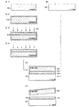
まず、半導体基板100を準備する(図1(A−1)参照)。
First, the
半導体基板100は、単結晶半導体基板や多結晶半導体基板を用いることができ、例えば、単結晶又は多結晶のシリコン基板や、ゲルマニウム基板、ガリウムヒ素やインジウムリン等の化合物半導体基板が挙げられる。市販のシリコン基板としては、直径5インチ(125mm)、直径6インチ(150mm)、直径8インチ(200mm)、直径12インチ(300mm)、直径16インチ(400mm)サイズの円形のものが代表的である。なお、形状は円形に限られず矩形状等に加工したシリコン基板を用いることも可能である。以下の説明では、半導体基板100として、単結晶シリコン基板を用いる場合について示す。
As the
なお、半導体基板100の表面をあらかじめ硫酸過水(SPM)、アンモニア過水(APM)、塩酸過水(HPM)、希フッ酸(DHF)などを用いて適宜洗浄することが好ましい。
Note that the surface of the
次に、半導体基板100に熱酸化処理を行うことにより酸化膜102(ここでは、酸化シリコン(SiOx)膜)を形成する(図1(A−2)参照)。また、熱酸化処理は、酸化性雰囲気中にハロゲンを添加して行う。 Next, an oxide film 102 (here, a silicon oxide (SiOx) film) is formed by performing thermal oxidation treatment on the semiconductor substrate 100 (see FIG. 1A-2). The thermal oxidation treatment is performed by adding halogen in an oxidizing atmosphere.
本実施の形態では、塩素(Cl)ガスが導入された酸化雰囲気中で半導体基板100に熱酸化処理を行うことにより塩素酸化された酸化膜102を形成する。従って、酸化膜102は、塩素原子を含有した膜となる。
In this embodiment, the
酸化膜102中に含有された塩素原子は、歪みを形成してSi−O結合を切り、膜中に微小な空孔を形成することにより、酸化膜102を低密度化させている。その結果、酸化膜102の水分に対する吸収割合が向上し、拡散速度が増大する。つまり、酸化膜102表面に水分が存在する場合に、当該酸化膜102の表面に存在する水分を酸化膜102の膜中に素早く吸収し、拡散させることができる。
Chlorine atoms contained in the
また、酸化膜102に含有させるハロゲン原子としては塩素原子を含有させることが好ましい。これは、塩素原子を含有させることによって、界面準位を低減し、酸化膜の品質を向上することができるためである。また、酸化膜102に塩素原子に加えてフッ素原子を含有させてもよい。半導体基板100表面をフッ素酸化するには、半導体基板100表面にHF溶液に浸漬した後に酸化性雰囲気中で熱酸化処理を行うことや、HFを酸化性雰囲気に添加して熱酸化処理を行えばよい。
Further, it is preferable that a chlorine atom is contained as a halogen atom contained in the
熱酸化処理の一例としては、酸素に対し塩化水素(HCl)を0.5〜10体積%(好ましくは2体積%)の割合で含む酸化性雰囲気中で、900℃〜1150℃の温度(代表的には1000℃)で熱酸化(HCl酸化)を行うと良い。処理時間は0.1〜6時間、好ましくは0.5〜1時間とすればよい。形成される酸化膜の膜厚としては、10nm〜1000nm(好ましくは50nm〜300nm)、例えば100nmの厚さとする。このように、900℃〜1150℃の温度で熱酸化処理をおこなうことにより、酸化膜102との界面近傍における半導体基板100に含まれる酸素等の不純物を低減することができる。
As an example of the thermal oxidation treatment, a temperature of 900 ° C. to 1150 ° C. (typical) in an oxidizing atmosphere containing hydrogen chloride (HCl) at a ratio of 0.5 to 10% by volume (preferably 2% by volume) with respect to oxygen. Specifically, thermal oxidation (HCl oxidation) is preferably performed at 1000 ° C.). The treatment time may be 0.1 to 6 hours, preferably 0.5 to 1 hour. The thickness of the oxide film to be formed is 10 nm to 1000 nm (preferably 50 nm to 300 nm), for example, 100 nm. As described above, by performing the thermal oxidation treatment at a temperature of 900 ° C. to 1150 ° C., impurities such as oxygen contained in the
熱酸化処理の他の一例としては、酸素に対し、トランス−1,2−ジクロロエチレン(DCE)を0.25〜5体積%(好ましくは3体積%)の割合で含む酸化性雰囲気中で、700℃〜1150℃の温度(代表的には950℃)で熱酸化を行うとよい。処理時間は0.1〜6時間、好ましくは0.5〜1時間とすればよい。形成される酸化膜の膜厚としては、10nm〜1000nm(好ましくは50nm〜300nm)、例えば100nmの厚さとする。トランス1,2ジクロロエチレンは熱分解する温度が低いため、熱酸化処理の温度を低温で行いたい場合に有効となる。なお、トランス−1,2−ジクロロエチレンにかえて、シス−1,2−ジクロロエチレン、1,1−ジクロロエチレンや、これらの中から二種類以上のガスの混合ガスを用いてもよい。
Another example of the thermal oxidation treatment is 700 in an oxidizing atmosphere containing trans-1,2-dichloroethylene (DCE) at a ratio of 0.25 to 5% by volume (preferably 3% by volume) with respect to oxygen. Thermal oxidation may be performed at a temperature of 1 ° C. to 1150 ° C. (typically 950 ° C.). The treatment time may be 0.1 to 6 hours, preferably 0.5 to 1 hour. The thickness of the oxide film to be formed is 10 nm to 1000 nm (preferably 50 nm to 300 nm), for example, 100 nm. Since
本実施の形態では、酸化膜102に含まれる塩素原子の濃度を1×10¹⁷/cm3〜1×1021/cm3となるように制御する。また、半導体基板100との界面に塩素原子が多く含まれるように(半導体基板100との界面付近に濃度のピークがくるように)する。このように界面付近に塩素原子を多く含ませることによって、界面準位を低減できる。
In this embodiment, the concentration of chlorine atoms contained in the
また、酸化膜102に塩素原子を含有させることによって、外因性不純物である重金属を捕集して半導体基板が汚染されることを防止する効果を奏する。このような重金属として、Fe、Cr、Ni、Mo等があり、これらは半導体基板に対し、質量分離されないイオンをドーピングして脆化領域を形成する場合に導入される。すなわち、HCl酸化などによって膜中にハロゲンを含有させた酸化膜102は、重金属など半導体基板に悪影響を与える不純物をゲッタリングする作用がある。酸化膜102を形成した後に行われる熱処理により、半導体基板に含まれる不純物としての金属は酸化膜102に析出し、ハロゲン(例えば塩素)と反応して捕獲されることとなる。それにより酸化膜102中に捕集した当該不純物を固定して半導体基板100の汚染を防ぐことができる。また、酸化膜102はガラス基板と貼り合わせた場合に、ガラスに含まれるNa等の不純物に対するブロッキング膜としても機能しうる。
In addition, the inclusion of chlorine atoms in the
また、熱酸化処理のガスに水素を含有させることにより、半導体基板100と酸化膜102の界面の欠陥を補償して界面の局在準位密度を低減する作用を奏する。そのため、酸化膜102中に水素原子が1×10¹⁸/cm3以上含まれるようにすることが好ましい。
In addition, by containing hydrogen in the gas for thermal oxidation treatment, defects at the interface between the
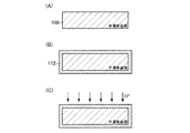
本実施の形態では、塩素原子を含有する酸化膜102の形成方法として、塩化水素やジクロロエチレンを含有させた酸化性雰囲気中で熱酸化処理を行う場合を示したが、これに限られない。例えば、半導体基板100に酸化性雰囲気で熱酸化処理を行い、半導体基板100表面に酸化膜112(例えば、SiOx)を形成した後(図2(A)、(B)参照)、イオンドーピング装置又はイオン注入装置を用いて、電界で加速された塩素イオンを添加することにより酸化膜112中に塩素原子を含有させてもよい(図2(C)参照)。他にも、表面を塩化水素の水溶液(塩酸)で処理した後に酸化性雰囲気中で熱酸化処理を行ってもよい。
In this embodiment mode, the case where the thermal oxidation treatment is performed in an oxidizing atmosphere containing hydrogen chloride or dichloroethylene is shown as a method for forming the
次に、運動エネルギーを有するイオンを半導体基板100に照射することで、半導体基板100の所定の深さに結晶構造が損傷された脆化領域104を形成する(図1(A−3)参照)。図1(A−3)に示すように、酸化膜102を介して、加速されたイオン103を半導体基板100に照射することで、半導体基板100の表面から所定の深さの領域にイオン103が導入され、脆化領域104を形成することができる。イオン103は、ソースガスを励起して、ソースガスのプラズマを生成し、このプラズマに含まれるイオンを、電界の作用によりプラズマから引き出して、加速したイオンである。
Next, the
脆化領域104が形成される領域の深さは、イオン103の運動エネルギー、質量、イオン103の入射角によって調節することができる。運動エネルギーは加速電圧、ドーズ量などにより調節できる。イオン103の平均侵入深さとほぼ同じ深さの領域に脆化領域104が形成される。そのため、イオン103を添加する深さで、半導体基板100から分離される半導体層の厚さが決定される。この半導体層の厚さが110nm以上500nm以下、好ましくは50nm以上200nm以下になるように、脆化領域104が形成される深さを調節する。
The depth of the region where the embrittled
脆化領域104の形成は、イオンドーピング処理で行うことができる。イオンドーピング処理には、イオンドーピング装置を用いて行うことができる。イオンドーピング装置の代表的な装置は、プロセスガスをプラズマ励起して生成された全てのイオン種をチャンバー内に配置された被処理体に照射する非質量分離型の装置である。非質量分離型の装置であるのは、プラズマ中のイオン種を質量分離しないで、全てのイオン種を被処理体に照射しているからである。これに対して、イオン注入装置は質量分離型の装置である。イオン注入装置は、プラズマ中のイオン種を質量分離し、ある特定の質量のイオン種を被処理体に照射する装置である。
The
イオンドーピング装置の主要な構成は、被処理物を配置するチャンバー、所望のイオンを発生させるイオン源、およびイオンを加速し、照射するための加速機構である。イオン源は、所望のイオン種を生成するためのソースガスを供給するガス供給装置、ソースガスを励起して、プラズマを生成させるための電極などで構成される。プラズマを形成するための電極として、フィラメント型の電極や容量結合高周波放電用の電極などが用いられる。加速機構は、引出電極、加速電極、減速電極、接地電極等の電極など、およびこれらの電極に電力を供給するための電源などで構成される。加速機構を構成する電極には複数の開口やスリットが設けられており、イオン源で生成されたイオンは電極に設けられた開口やスリットを通過して加速される。なお、イオンドーピング装置の構成は上述したものに限定されず、必要に応じた機構が設けられる。 The main components of the ion doping apparatus are a chamber in which an object to be processed is arranged, an ion source for generating desired ions, and an acceleration mechanism for accelerating and irradiating ions. The ion source includes a gas supply device that supplies a source gas for generating a desired ion species, an electrode for generating a plasma by exciting the source gas, and the like. As an electrode for forming plasma, a filament-type electrode, an electrode for capacitively coupled high-frequency discharge, or the like is used. The acceleration mechanism includes an electrode such as an extraction electrode, an acceleration electrode, a deceleration electrode, and a ground electrode, and a power source for supplying power to these electrodes. The electrode constituting the acceleration mechanism is provided with a plurality of openings and slits, and ions generated by the ion source are accelerated through the openings and slits provided in the electrodes. Note that the configuration of the ion doping apparatus is not limited to that described above, and a mechanism according to need is provided.
本実施形態では、イオンドーピング装置で、水素を半導体基板100に添加する。プラズマソースガスとして水素を含むガスを供給する。例えば、H2を供給する。水素ガスを励起してプラズマを生成し、質量分離せずに、プラズマ中に含まれるイオンを加速し、加速されたイオンを半導体基板100に照射する。
In this embodiment, hydrogen is added to the
イオンドーピング装置において、水素ガスから生成されるイオン種(H+、H2 +、H3 +)の総量に対してH3 +の割合が50%以上とする。より好ましくは、そのH3 +の割合を80%以上とする。イオンドーピング装置は質量分離を行わないため、プラズマ中に生成される複数のイオン種のうち、1つを50%以上とすることが好ましく、80%以上とすることが好ましい。同じ質量のイオンを照射することで、半導体基板100の同じ深さに集中させてイオンを添加することができる。
In the ion doping apparatus, the ratio of H 3 + to the total amount of ion species (H + , H 2 + , H 3 + ) generated from hydrogen gas is 50% or more. More preferably, the ratio of H 3 + is 80% or more. Since the ion doping apparatus does not perform mass separation, one of the plurality of ion species generated in the plasma is preferably 50% or more, and more preferably 80% or more. By irradiating ions with the same mass, ions can be added while being concentrated at the same depth of the
脆化領域104を浅い領域に形成するためには、イオン103の加速電圧を低くする必要があるが、プラズマ中のH3 +イオンの割合を高くすることで、原子状水素(H)を効率よく、半導体基板100に添加できる。H3 +イオンはH+イオンの3倍の質量を持つことから、同じ深さに水素原子を1つ添加する場合、H3 +イオンの加速電圧は、H+イオンの加速電圧の3倍にすることが可能となる。イオンの加速電圧を大きくできれば、イオンの照射工程のタクトタイムを短縮することが可能となり、生産性やスループットの向上を図ることができる。
In order to form the embrittled
また、加速されたイオン103を半導体基板100に照射する工程は、イオン注入装置で行うこともできる。イオン注入装置は、チャンバー内に配置された被処理体に、ソースガスをプラズマ励起して生成された複数のイオン種を質量分離し、特定のイオン種を照射する質量分離型の装置である。したがって、イオン注入装置を用いる場合は、水素ガスを励起して生成されたH+イオンおよびH2 +イオンを質量分離して、H+イオンまたはH2 +イオンの一方のイオンを加速して、半導体基板100に照射する。
The step of irradiating the
次に、半導体基板100上に形成された酸化膜102の表面にプラズマ処理を行うことが好ましい(図1(A−4)参照)。
Next, plasma treatment is preferably performed on the surface of the
プラズマ処理は、真空状態のチャンバーに不活性ガス(例えば、アルゴン(Ar)ガス)及び/又は反応性ガス(例えば、酸素(O2)ガス、窒素(N2)ガス)を導入し、基板が設けられた電極と対向電極間に高周波電圧を印加して(バイアス電圧が加わった状態として)、被処理面にプラズマ処理を行う。 In the plasma treatment, an inert gas (eg, argon (Ar) gas) and / or a reactive gas (eg, oxygen (O 2 ) gas, nitrogen (N 2 ) gas) is introduced into a vacuum chamber, and the substrate is A high-frequency voltage is applied between the provided electrode and the counter electrode (assuming a bias voltage is applied), and plasma processing is performed on the surface to be processed.
例えば、酸素プラズマ処理を行う場合、真空状態のチャンバーに酸素ガスを導入し、半導体基板100が設けられた電極と対向電極間に高周波電圧を印加して(バイアス電圧が加わった状態として)、酸化膜102にプラズマ処理を行う。プラズマ中には酸素の陽イオンが存在し、陰極方向(半導体基板100側)に酸素の陽イオンが加速される。加速された酸素の陽イオンが半導体基板100上の酸化膜102表面に衝突することによって、酸化膜102表層のSi−O結合を切り低密度化すると共に、ダングリングボンドを生成して表面を活性化することができる。
For example, when oxygen plasma treatment is performed, oxygen gas is introduced into a vacuum chamber, a high-frequency voltage is applied between the electrode provided with the
本実施の形態では、酸素ガスを用いて、容量結合プラズマの一種でRIE(リアクティブイオンエッチング)モードと呼ばれる方式のプラズマ処理で行う。半導体基板100を、コンデンサを介して高周波電圧が印加される陰極電極上のステージに設置し、高周波電圧を印加してプラズマを生成する。その結果、自己バイアスが発生し(バイアスが印加された状態となり)、プラズマ中の陽イオンが加速されて半導体基板100に衝突する。なお、ここでは、原料ガスが酸素であり、半導体基板100上に形成された酸化膜102が酸化シリコンであるため、エッチング作用は少ない。
In this embodiment mode, oxygen gas is used, which is a kind of capacitively coupled plasma, which is performed by a plasma treatment of a method called an RIE (reactive ion etching) mode. The
なお、酸素プラズマの具体的な条件としては、処理電力0.1〜1.5W/cm2、圧力30〜130Pa、ガス(O2)流量10〜200sccmで行えばよい。また、プラズマ処理において、窒素ガスやアルゴンガスを用いる場合にも同様の条件で行うことができる。 Note that specific conditions of the oxygen plasma may be performed at a processing power of 0.1 to 1.5 W / cm 2 , a pressure of 30 to 130 Pa, and a gas (O 2 ) flow rate of 10 to 200 sccm. In addition, the plasma treatment can be performed under the same conditions when nitrogen gas or argon gas is used.
また、酸素プラズマ処理を行うことにより、酸化膜102の表面の平均粗さ(Ra)を好ましくは0.7nm以下、より好ましくは0.3nm以下とする。
Further, by performing oxygen plasma treatment, the average roughness (Ra) of the surface of the
次に、ベース基板120を準備する(図1(B)参照)。
Next, the
ベース基板120は、絶縁体でなる基板を用いる。具体的には、アルミノシリケートガラス、アルミノホウケイ酸ガラス、バリウムホウケイ酸ガラスのような電子工業用に使われる各種ガラス基板、石英基板、セラミック基板、サファイア基板が挙げられる。本実施の形態では、ガラス基板を用いる場合について説明する。ベース基板120として大面積化が可能で安価なガラス基板を用いることにより、シリコンウエハを用いる場合と比較して低コスト化を図ることができる。
As the
また、ベース基板120を用いるに際し、ベース基板120の表面をあらかじめ洗浄することが好ましい。具体的には、ベース基板120を、塩酸過水(HPM)、硫酸過水(SPM)、アンモニア過水(APM)、希フッ酸(DHF)等を用いて超音波洗浄を行う。例えば、ベース基板120の表面に塩酸過水を用いて超音波洗浄を行うことが好ましい。このような洗浄処理を行うことによって、ベース基板120表面の平坦化や残存する研磨粒子を除去することができる。
In using the
次に、半導体基板100とベース基板120とを対向させ、酸化膜102表面とベース基板120表面とを接合させる(図1(C)参照)。
Next, the
ここでは、半導体基板100とベース基板120を密着させた後、半導体基板100の端の一箇所に1〜500N/cm2、好ましくは1〜20N/cm2程度の圧力を加える。圧力を加えた部分から酸化膜102とベース基板120とが接合しはじめ、自発的に接合が形成され全面におよぶ。この接合工程は、ファンデルワールス力や水素結合が作用しており、加熱処理を伴わず、常温で行うことができるため、ベース基板120に、ガラス基板のように耐熱温度が低い基板を用いることができる。
Here, after close contact with the
なお、半導体基板100とベース基板120を接合させる前に、半導体基板100上に形成された酸化膜102と、ベース基板120の表面処理を行うことが好ましい。表面処理としては、オゾン処理(例えば、オゾン水洗浄)やメガソニック洗浄、又はこれらを組み合わせて行うことができる。また、オゾン水洗浄とフッ酸による洗浄を複数回繰り返し行ってもよい。このような表面処理を行うことにより、酸化膜102、ベース基板120表面の有機物等のゴミを除去し、表面を親水化することができる。
Note that before the
ベース基板120に半導体基板100を接合させた後、ベース基板120と酸化膜102との接合強度を増加させるための熱処理を行うことが好ましい。この熱処理の温度は、脆化領域104に亀裂を発生させない温度とし、室温以上400℃未満の温度範囲で処理することができる。また、この温度範囲で加熱しながら、ベース基板120に半導体基板100を貼り合わせることで、ベース基板120と酸化膜102との接合界面での接合強度を強固にすることができる。熱処理には、拡散炉、抵抗加熱炉などの加熱炉、RTA(瞬間熱アニール、Rapid Thermal Anneal)装置、マイクロ波加熱装置などを用いることができる。
After the
通常、このような温度で熱処理を行った場合には、接合強度をある程度は増加させることは可能であるが、十分な接合強度を得ることは難しい。これは、半導体基板とベース基板を接合させた後に熱処理を行うと、接合界面において脱水縮合反応が生じ共有結合が形成されることにより接合が強化されるが、脱水縮合反応を促進させるためには、脱水縮合反応により接合界面に生じる水分を高温で熱処理を行うことにより除去する必要があるためである。つまり、接合後の熱処理温度を高くすることにより、脱水縮合反応で接合界面に生じた水分を除去し接合強度を向上させることができるが、熱処理温度が低い場合には、脱水縮合反応で接合界面に生じた水分を効果的に除去できないため、脱水縮合反応が進まず接合強度を十分に向上させることができない。 Usually, when heat treatment is performed at such a temperature, it is possible to increase the bonding strength to some extent, but it is difficult to obtain a sufficient bonding strength. This is because when a heat treatment is performed after bonding the semiconductor substrate and the base substrate, a dehydration condensation reaction occurs at the bonding interface and a covalent bond is formed, thereby strengthening the bonding. To promote the dehydration condensation reaction, This is because it is necessary to remove the water generated at the bonding interface by the dehydration condensation reaction by performing a heat treatment at a high temperature. In other words, by increasing the heat treatment temperature after bonding, moisture generated at the bonding interface by the dehydration condensation reaction can be removed and the bonding strength can be improved. However, if the heat treatment temperature is low, the bonding interface can be removed by the dehydration condensation reaction. Since the moisture generated in the film cannot be removed effectively, the dehydration condensation reaction does not proceed and the bonding strength cannot be sufficiently improved.
しかし、本実施の形態では、上述したように酸化膜102に塩素原子を含有させることによって、当該酸化膜102が水分を吸収し効果的に拡散させることができるため、熱処理の温度が低い場合であっても、脱水縮合反応で接合界面に生じた水分を酸化膜102へ吸収、拡散させ脱水縮合反応を効率良く促進させることができる。従って、接合後の熱処理を低温で行った場合であっても、半導体基板100上の酸化膜102とベース基板120の接合強度を十分に向上させることが可能となる。
However, in this embodiment, when the
また、酸化膜102の表面は、脆化領域104を形成する際のイオンの照射や酸化膜102表面に対するプラズマ処理によりダングリングボンドが形成され、表面が活性な状態となっているため、低温であってもベース基板120と強固な接合を形成することができる。
Further, the surface of the
次に、熱処理を行い脆化領域104にて分離することにより、ベース基板120上に、酸化膜102を介して半導体膜(ここでは、単結晶半導体膜124)を設ける(図1(D)参照)。
Next, heat treatment is performed and separation is performed in the embrittled
加熱処理を行うことで、温度上昇によって脆化領域104に形成されている微小な孔には、イオンドーピングで添加した元素が析出し、内部の圧力が上昇する。圧力の上昇により、脆化領域104に亀裂が生じるので、脆化領域104に沿って半導体基板100が分離する。酸化膜102はベース基板120に接合しているので、ベース基板120上には半導体基板100から分離された単結晶半導体膜124が形成される。また、ここでの熱処理の温度は、ベース基板120の歪み点を越えない温度とする。
By performing the heat treatment, the element added by ion doping is precipitated in the minute holes formed in the embrittled
この加熱処理には、拡散炉、抵抗加熱炉などの加熱炉、RTA(瞬間熱アニール、Rapid Thermal Anneal)装置、マイクロ波加熱装置などを用いることができる。例えば、RTA装置を用いる、加熱温度550℃以上700℃以下、処理時間0.5分以上60分以内で行うことができる。 For this heat treatment, a heating furnace such as a diffusion furnace or a resistance heating furnace, a rapid thermal annealing (RTA) apparatus, a microwave heating apparatus, or the like can be used. For example, the heating can be performed using an RTA apparatus at a heating temperature of 550 ° C. to 700 ° C. and a processing time of 0.5 minutes to 60 minutes.
このように、半導体基板100上の酸化膜102とベース基板120とを接合させた後に、複数回に渡って熱処理をおこなうことよって、接合強度を増加させることができる。なお、上述したベース基板120と酸化膜102との接合強度を増加させるための熱処理を行わず、図1(D)の熱処理を行うことにより、ベース基板120と酸化膜102との接合強度の増加の熱処理工程と、脆化領域104における分離の熱処理工程を同時に行ってもよい。同時に行った場合であっても、酸化膜102に塩素原子を含有させることによって、熱処理時において脱水縮合反応で接合界面に生じた水分を酸化膜102へ吸収、拡散させ脱水縮合反応を効率良く促進させることができる。その結果、半導体基板100上の酸化膜102とベース基板120の接合強度を十分に向上させることが可能となる。
As described above, the bonding strength can be increased by performing heat treatment a plurality of times after the
以上の工程により、ベース基板120上に酸化膜102を介して単結晶半導体膜124が設けられたSOI基板を作製することができる。本実施の形態で示した作製方法を用いることによって、膜の形成にCVD法やスパッタリング法による成膜工程が不要となるため、CVD法やスパッタリング法を用いた成膜により生じるゴミの発生を防止することができる。その結果、ゴミの影響による半導体基板とベース基板の貼り合わせ不良を抑制することができる。
Through the above steps, an SOI substrate in which the single
また、半導体基板に対するHCl熱酸化は、当該半導体基板に形成された積層欠陥の収縮・消滅に有効となる。したがって、SOI基板の製造プロセスにおいて、半導体基板を繰り返し(再生して)用いる場合には、半導体基板の積層欠陥が問題となるが、SOI基板の製造プロセスにおいてHCl酸化を行うことによりこのような問題を解決することができる。 Further, the thermal oxidation of HCl on a semiconductor substrate is effective for contraction / elimination of stacking faults formed on the semiconductor substrate. Therefore, when a semiconductor substrate is used repeatedly (regenerated) in the manufacturing process of an SOI substrate, stacking faults of the semiconductor substrate become a problem, but such a problem is caused by performing HCl oxidation in the manufacturing process of the SOI substrate. Can be solved.
なお、上記工程において、得られたSOI基板の表面に平坦化処理を行ってもよい。平坦化処理を行うことにより、分離後にベース基板120上に設けられた単結晶半導体膜124の表面に凹凸が生じた場合でもSOI基板の表面を平坦化することができる。
Note that in the above steps, planarization treatment may be performed on the surface of the obtained SOI substrate. By performing the planarization treatment, the surface of the SOI substrate can be planarized even when unevenness is generated on the surface of the single
平坦化処理としては、CMP(Chemical Mechanical Polishing)、エッチング処理、レーザー光の照射等により行うことができる。ここでは、ドライエッチングまたはウエットエッチングの一方、または双方を組み合わせたエッチング処理(エッチバック処理)を行った後にレーザー光を照射することによって、単結晶半導体膜124の再結晶化と表面の平坦化を行う。
The planarization treatment can be performed by CMP (Chemical Mechanical Polishing), etching treatment, laser light irradiation, or the like. Here, the single
レーザー光を単結晶半導体膜の上面側から照射することで、単結晶半導体膜の上面を溶融させることができる。溶融した後、単結晶半導体膜が冷却、固化することで、その上面の平坦性が向上した単結晶半導体膜が得られる。レーザー光を用いることにより、ベース基板120が直接加熱されないため、当該ベース基板120の温度上昇を抑えることができる。このため、ガラス基板のような耐熱性の低い基板をベース基板120に用いることが可能である。
By irradiating laser light from the upper surface side of the single crystal semiconductor film, the upper surface of the single crystal semiconductor film can be melted. After melting, the single crystal semiconductor film is cooled and solidified, whereby a single crystal semiconductor film with improved flatness on the upper surface is obtained. By using laser light, the
なお、レーザー光の照射による単結晶半導体膜124の溶融は、部分溶融とすることが好ましい。完全溶融させた場合には、液相となった後の無秩序な核発生により微結晶化し、結晶性が低下する可能性が高いためである。一方で、部分溶融させることにより、溶融されていない固相部分から結晶成長が進行する。これにより、半導体膜中の欠陥を減少させることができる。ここで、完全溶融とは、単結晶半導体膜が下部界面付近まで溶融されて、液体状態になることをいう。他方、部分溶融とは、この場合、単結晶半導体膜の上部は溶融して液相となるが、下部は溶融せずに固相のままであることをいう。
Note that melting of the single
上記レーザー光の照射には、パルス発振レーザーを用いることが好ましい。これは、瞬間的に高エネルギーのパルスレーザー光を発振することができ、溶融状態を作り出すことが容易となるためである。発振周波数は、1Hz以上10MHz以下程度とすることが好ましい。 A pulsed laser is preferably used for the laser light irradiation. This is because high-energy pulsed laser light can be instantaneously oscillated, and it becomes easy to create a molten state. The oscillation frequency is preferably about 1 Hz to 10 MHz.
上述のようにレーザー光を照射した後には、単結晶半導体膜124の膜厚を小さくする薄膜化工程を行っても良い。単結晶半導体膜124の薄膜化には、ドライエッチングまたはウエットエッチングの一方、または双方を組み合わせたエッチング処理(エッチバック処理)を適用すればよい。例えば、単結晶半導体膜124がシリコン材料からなる層である場合、ドライエッチングとしてSF6とO2をプロセスガスに用いて、単結晶半導体膜124を薄くすることができる。
After the laser light irradiation as described above, a thinning process for reducing the thickness of the single
なお、平坦化処理はSOI基板に限らず分離後の半導体基板100に対して行ってもよい。分離後の半導体基板100の表面を平坦にすることによって、当該半導体基板100をSOI基板の作製工程において再利用することが可能となる。
Note that the planarization process may be performed not only on the SOI substrate but also on the
なお、本実施の形態で示したSOI基板の作製方法は、本明細書の他の実施の形態で示す作製方法と適宜組み合わせて行うことができる。 Note that the method for manufacturing an SOI substrate described in this embodiment can be combined with manufacturing methods described in other embodiments in this specification as appropriate.
(実施の形態2)
本実施の形態では、上記実施の形態と異なるSOI基板の作製方法に関して図面を参照して説明する。具体的には、ベース基板の表面に絶縁膜を形成する場合について説明する。
(Embodiment 2)
In this embodiment, a method for manufacturing an SOI substrate, which is different from that in the above embodiment, will be described with reference to drawings. Specifically, a case where an insulating film is formed on the surface of the base substrate will be described.
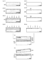
まず、半導体基板100上に酸化膜102を形成し、イオンビームを照射することにより脆化領域104を形成した後、酸化膜102の表面に酸素プラズマ処理を行う(図3(A−1)〜(A−4)参照)。なお、図3(A−1)〜(A−4)の具体的な作製工程については、上記図1(A−1)〜(A−4)において示した方法を適用すればよいため、詳しい説明を省略する。
First, an
次に、ベース基板120を準備する(図3(B−1)参照)。そして、ベース基板120に、半導体膜121を形成した後(図3(B−2)参照)、ジクロロエチレンを含有させた酸化性雰囲気で熱酸化処理を行うことにより、表面に塩素原子を含有する酸化膜122を形成する(図3(B−3)参照)。
Next, the
例えば、ベース基板120として歪点が730℃のガラス基板を用い、当該ガラス基板上に半導体膜を形成する。その後、酸素に対しトランス−1,2−ジクロロエチレン(DCE)を1〜5体積%(好ましくは2体積%)の割合で含む酸化性雰囲気中で、700℃〜730℃の温度(代表的には720℃)で熱酸化処理を行うことによって、ベース基板120表面の塩素酸化を行う。その結果、ベース基板120上に塩素原子を含有する酸化膜122が形成される。形成される酸化膜の膜厚としては、10nm〜1000nm(好ましくは50nm〜300nm)、例えば100nmの厚さとする。トランス1,2ジクロロエチレンは熱分解する温度が低いため、耐熱温度が低い基板(例えば、ガラス基板)に熱酸化処理を行う場合に用いることができる。
For example, a glass substrate having a strain point of 730 ° C. is used as the
半導体膜121は、スパッタ法、LPCVD法、プラズマCVD法等により、25〜200nm(好ましくは30〜150nm)の厚さで形成する。例えば、非晶質シリコン膜を形成すればよい。
The
つまり、本実施の形態では、ベース基板120として、表面に塩素酸化及び/又はフッ素酸化された酸化膜が形成された基板を用いる。
In other words, in this embodiment, a substrate having a surface on which an oxide film that has been oxidized with chlorine and / or fluorine is formed is used as the
他にも、ベース基板120上に半導体膜121(例えば、シリコン膜)を形成した後、塩素(Cl)及び/又はフッ素が添加された酸化雰囲気中で熱酸化処理を行うことにより、半導体膜121を塩素酸化及び/又はフッ素酸化することにより酸化膜122を形成してもよい。
In addition, after the semiconductor film 121 (eg, a silicon film) is formed over the
なお、ベース基板120上に酸化膜122を形成した後、当該酸化膜122表面にプラズマ処理を行うことが好ましい(図3(B−3)参照)。
Note that after the
プラズマ処理は、真空状態のチャンバーに不活性ガス(例えば、アルゴン(Ar)ガス)及び/又は反応性ガス(例えば、酸素(O2)ガス、窒素(N2)ガス)を導入し、基板が設けられた電極と対向電極間に高周波電圧を印加して(バイアス電圧が加わった状態として)、被処理面にプラズマ処理を行う。例えば、酸素プラズマ処理を行う場合、真空状態のチャンバーに酸素ガスを導入し、ベース基板120が設けられた電極と対向電極間に高周波電圧を印加して(バイアス電圧が加わった状態として)、酸化膜122にプラズマ処理を行う。プラズマ中には酸素の陽イオンが存在し、陰極方向(ベース基板120側)に酸素の陽イオンが加速される。加速された酸素の陽イオンがベース基板120表面に衝突することによって、酸化膜122表層のSi−O結合を切り低密度化すると共に、ダングリングボンドを生成して表面を活性化することができる。
In the plasma treatment, an inert gas (eg, argon (Ar) gas) and / or a reactive gas (eg, oxygen (O 2 ) gas, nitrogen (N 2 ) gas) is introduced into a vacuum chamber, and the substrate is A high-frequency voltage is applied between the provided electrode and the counter electrode (assuming a bias voltage is applied), and plasma processing is performed on the surface to be processed. For example, when oxygen plasma treatment is performed, oxygen gas is introduced into a vacuum chamber, a high-frequency voltage is applied between the electrode provided with the
次に、半導体基板100とベース基板120とを対向させ、酸化膜102表面と酸化膜122表面とを接合させる(図3(C)参照)。その後、熱処理を行い脆化領域104にて分離することにより、ベース基板120上に、酸化膜122及び酸化膜102を介して単結晶半導体膜124を設ける(図3(D)参照)。
Next, the
本実施の形態では、接合面となる酸化膜102及び酸化膜122が塩素原子を含有する酸化膜となっているため、接合後の熱処理において脱水縮合反応で接合界面に生じた水分子を酸化膜102及び酸化膜122へ拡散させ脱水縮合反応を促進させることができる。さらに、酸化膜102の表面は、脆化領域104を形成する際のイオンの照射や酸化膜102表面に対するプラズマ処理によりダングリングボンドが形成され、表面が活性な状態となっている。従って、接合後の熱処理をガラス基板の歪点以下の温度で行った場合であっても、接合強度を十分に向上させることが可能となる。
In this embodiment, since the
なお、本実施の形態では、半導体基板100に形成する酸化膜102として塩素原子を含有する酸化膜としたが、これに限られない。例えば、半導体基板100に酸化性雰囲気で熱酸化処理して得られた酸化膜を酸化膜102として適用することができる。
In the present embodiment, the
また、本実施の形態では、塩素原子を含有する酸化膜122の形成方法として、ベース基板120上に半導体膜121を形成した後、ジクロロエチレンを含有させた酸化性雰囲気中で熱酸化処理を行う場合を示したが、これに限られない。例えば、ベース基板120に、イオンドーピング装置又はイオン注入装置を用いて、電界で加速された塩素イオンを添加することにより、ベース基板120表面近傍に塩素原子を導入してもよい。他にも、ジクロロエチレンを含有させた酸化性雰囲気中でベース基板120表面に熱酸化処理を行ってもよい。
In this embodiment, as a method for forming the
なお、本実施の形態で示したSOI基板の作製方法は、本明細書の他の実施の形態で示す作製方法と適宜組み合わせて行うことができる。 Note that the method for manufacturing an SOI substrate described in this embodiment can be combined with manufacturing methods described in other embodiments in this specification as appropriate.
(実施の形態3)
本実施の形態では、上記実施の形態で作製したSOI基板を用いて、半導体装置を作製する方法を説明する。
(Embodiment 3)
In this embodiment, a method for manufacturing a semiconductor device using the SOI substrate manufactured in the above embodiment will be described.
まず、図4および図5を参照して、nチャネル型薄膜トランジスタ、およびpチャネル型薄膜トランジスタを作製する方法を説明する。複数の薄膜トランジスタ(TFT)を組み合わせることで、各種の半導体装置を形成することができる。 First, a method for manufacturing an n-channel thin film transistor and a p-channel thin film transistor is described with reference to FIGS. Various semiconductor devices can be formed by combining a plurality of thin film transistors (TFTs).
SOI基板として、上記実施の形態1の方法で作製したSOI基板を用いる場合について説明する。もちろん、上記実施の形態2の方法で作製したSOI基板を用いることも可能である。
The case where an SOI substrate manufactured by the method of
図4(A)は、図1を用いて説明した方法で作製されたSOI基板の断面図である。 FIG. 4A is a cross-sectional view of an SOI substrate manufactured by the method described with reference to FIG.
エッチングにより、単結晶半導体膜124を素子分離して、図4(B)に示すように半導体膜251、252を形成する。半導体膜251はnチャネル型のTFTを構成し、半導体膜252はpチャネル型のTFTを構成する。
The single
図4(C)に示すように、半導体膜251、252上に絶縁膜254を形成する。次に、絶縁膜254を介して半導体膜251上にゲート電極255を形成し、半導体膜252上にゲート電極256を形成する。
As shown in FIG. 4C, an insulating
なお、単結晶半導体膜124のエッチングを行う前に、TFTのしきい値電圧を制御するために、ホウ素、アルミニウム、ガリウムなどの不純物元素、またはリン、ヒ素などの不純物元素を単結晶半導体膜124に添加することが好ましい。例えば、nチャネル型TFTが形成される領域に不純物元素を添加し、pチャネル型TFTが形成される領域に不純物元素を添加する。
Note that before the single
次に、図4(D)に示すように半導体膜251にn型の低濃度不純物領域257を形成し、半導体膜252にp型の高濃度不純物領域259を形成する。具体的には、まず、半導体膜251にn型の低濃度不純物領域257を形成する。このため、pチャネル型TFTとなる半導体膜252をレジストでマスクし、不純物元素を半導体膜251に添加する。不純物元素としてリンまたはヒ素を添加すればよい。イオンドーピング法またはイオン注入法により不純物元素を添加することにより、ゲート電極255がマスクとなり、半導体膜251に自己整合的にn型の低濃度不純物領域257が形成される。半導体膜251のゲート電極255と重なる領域はチャネル形成領域258となる。
Next, as illustrated in FIG. 4D, an n-type low
次に、半導体膜252を覆うマスクを除去した後、nチャネル型TFTとなる半導体膜251をレジストマスクで覆う。次に、イオンドーピング法またはイオン注入法により不純物元素を半導体膜252に添加する。不純物元素として、ボロンを添加することができる。不純物元素の添加工程では、ゲート電極256がマスクとして機能して、半導体膜252にp型の高濃度不純物領域259が自己整合的に形成される。高濃度不純物領域259はソース領域またはドレイン領域として機能する。半導体膜252のゲート電極256と重なる領域はチャネル形成領域260となる。ここでは、n型の低濃度不純物領域257を形成した後、p型の高濃度不純物領域259を形成する方法を説明したが、先にp型の高濃度不純物領域259を形成することもできる。
Next, after removing the mask covering the
次に、半導体膜251を覆うレジストを除去した後、プラズマCVD法等によって窒化シリコン等の窒素化合物や酸化シリコン等の酸化物からなる単層構造または積層構造の絶縁膜を形成する。この絶縁膜を垂直方向の異方性エッチングすることで、図5(A)に示すように、ゲート電極255、256の側面に接するサイドウォール絶縁膜261、262を形成する。この異方性エッチングにより、絶縁膜254もエッチングされる。
Next, after removing the resist covering the
次に、図5(B)に示すように、半導体膜252をレジスト265で覆う。半導体膜251にソース領域またはドレイン領域として機能する高濃度不純物領域を形成するため、イオン注入法またはイオンドーピング法により、半導体膜251に高ドーズ量で不純物元素を添加する。ゲート電極255およびサイドウォール絶縁膜261がマスクとなり、n型の高濃度不純物領域267が形成される。次に、不純物元素の活性化のための加熱処理を行う。
Next, as illustrated in FIG. 5B, the
活性化の加熱処理の後、図5(C)に示すように、水素を含んだ絶縁膜268を形成する。絶縁膜268を形成後、350℃以上450℃以下の温度による加熱処理を行い、絶縁膜268中に含まれる水素を半導体膜251、252中に拡散させる。絶縁膜268は、プロセス温度が350℃以下のプラズマCVD法により窒化シリコンまたは窒化酸化シリコンを堆積することで形成できる。半導体膜251、252に水素を供給することで、半導体膜251、252中および絶縁膜254との界面での捕獲中心となるような欠陥を効果的に補償することができる。
After the heat treatment for activation, an insulating
その後、層間絶縁膜269を形成する。層間絶縁膜269は、酸化シリコン膜、BPSG(Boron Phosphorus Silicon Glass)膜などの無機材料でなる絶縁膜、または、ポリイミド、アクリルなどの有機樹脂膜から選ばれた単層構造の膜、積層構造の膜で形成することができる。層間絶縁膜269にコンタクトホールを形成した後、図5(C)に示すように配線270を形成する。配線270の形成には、例えば、アルミニウム膜またはアルミニウム合金膜などの低抵抗金属膜をバリアメタル膜で挟んだ3層構造の導電膜で形成することができる。バリアメタル膜は、モリブデン、クロム、チタンなどの金属膜で形成することができる。
Thereafter, an
以上の工程により、nチャネル型TFTとpチャネル型TFTを有する半導体装置を作製することができる。SOI基板の作製過程で、チャネル形成領域を構成する半導体膜の金属元素の濃度を低減させているので、オフ電流が小さく、しきい値電圧の変動が抑制されたTFTを作製することができる。 Through the above steps, a semiconductor device having an n-channel TFT and a p-channel TFT can be manufactured. In the process of manufacturing the SOI substrate, the concentration of the metal element in the semiconductor film forming the channel formation region is reduced, so that a TFT with a small off-state current and a suppressed threshold voltage can be manufactured.
図4及び図5を参照してTFTの作製方法を説明したが、TFTの他、容量、抵抗などTFTと共に各種の半導体素子を形成することで、高付加価値の半導体装置を作製することができる。以下、図面を参照しながら半導体装置の具体的な態様を説明する。 Although the method for manufacturing a TFT has been described with reference to FIGS. 4 and 5, a semiconductor device with high added value can be manufactured by forming various semiconductor elements such as a capacitor and a resistor in addition to the TFT. . Hereinafter, specific embodiments of the semiconductor device will be described with reference to the drawings.
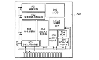
まず、半導体装置の一例として、マイクロプロセッサについて説明する。図6はマイクロプロセッサ500の構成例を示すブロック図である。
First, a microprocessor will be described as an example of a semiconductor device. FIG. 6 is a block diagram illustrating a configuration example of the
マイクロプロセッサ500は、演算回路501(Arithmetic logic unit。ALUともいう。)、演算回路制御部502(ALU Controller)、命令解析部503(Instruction Decoder)、割り込み制御部504(Interrupt Controller)、タイミング制御部505(Timing Controller)、レジスタ506(Register)、レジスタ制御部507(Register Controller)、バスインターフェース508(Bus I/F)、読み出し専用メモリ509、およびメモリインターフェース510を有している。
The
バスインターフェース508を介してマイクロプロセッサ500に入力された命令は、命令解析部503に入力され、デコードされた後、演算回路制御部502、割り込み制御部504、レジスタ制御部507、タイミング制御部505に入力される。演算回路制御部502、割り込み制御部504、レジスタ制御部507、タイミング制御部505は、デコードされた命令に基づき様々な制御を行う。
An instruction input to the
演算回路制御部502は、演算回路501の動作を制御するための信号を生成する。また、割り込み制御部504は、マイクロプロセッサ500のプログラム実行中に、外部の入出力装置や周辺回路からの割り込み要求を処理する回路であり、割り込み制御部504は、割り込み要求の優先度やマスク状態を判断して、割り込み要求を処理する。レジスタ制御部507は、レジスタ506のアドレスを生成し、マイクロプロセッサ500の状態に応じてレジスタ506の読み出しや書き込みを行う。タイミング制御部505は、演算回路501、演算回路制御部502、命令解析部503、割り込み制御部504、およびレジスタ制御部507の動作のタイミングを制御する信号を生成する。例えば、タイミング制御部505は、基準クロック信号CLK1を元に、内部クロック信号CLK2を生成する内部クロック生成部を備えている。図6に示すように、内部クロック信号CLK2は他の回路に入力される。
The arithmetic
次に、非接触でデータの送受信を行う機能、および演算機能を備えた半導体装置の一例を説明する。図7は、このような半導体装置の構成例を示すブロック図である。図7に示す半導体装置は、無線通信により外部装置と信号の送受信を行って動作するコンピュータ(以下、「RFCPU」という)と呼ぶことができる。 Next, an example of a semiconductor device having a function of performing transmission / reception of data without contact and an arithmetic function will be described. FIG. 7 is a block diagram illustrating a configuration example of such a semiconductor device. The semiconductor device illustrated in FIG. 7 can be referred to as a computer that operates by transmitting and receiving signals to and from an external device by wireless communication (hereinafter referred to as “RFCPU”).
図7に示すように、RFCPU511は、アナログ回路部512とデジタル回路部513を有している。アナログ回路部512として、共振容量を有する共振回路514、整流回路515、定電圧回路516、リセット回路517、発振回路518、復調回路519と、変調回路520と、電源管理回路530とを有している。デジタル回路部513は、RFインターフェース521、制御レジスタ522、クロックコントローラ523、CPUインターフェース524、中央処理ユニット525、ランダムアクセスメモリ526、読み出し専用メモリ527を有している。
As illustrated in FIG. 7, the
RFCPU511の動作の概要は以下の通りである。アンテナ528が受信した信号は共振回路514により誘導起電力を生じる。誘導起電力は、整流回路515を経て容量部529に充電される。この容量部529はセラミックコンデンサーや電気二重層コンデンサーなどのキャパシタで形成されていることが好ましい。容量部529は、RFCPU511を構成する基板に集積されている必要はなく、他の部品としてRFCPU511に組み込むこともできる。
The outline of the operation of the
リセット回路517は、デジタル回路部513をリセットし初期化する信号を生成する。例えば、電源電圧の上昇に遅延して立ち上がる信号をリセット信号として生成する。発振回路518は、定電圧回路516により生成される制御信号に応じて、クロック信号の周波数とデューティー比を変更する。復調回路519は、受信信号を復調する回路であり、変調回路520は、送信するデータを変調する回路である。
The
例えば、復調回路519はローパスフィルタで形成され、振幅変調(ASK)方式の受信信号を、その振幅の変動をもとに、二値化する。また、送信データを振幅変調(ASK)方式の送信信号の振幅を変動させて送信するため、変調回路520は、共振回路514の共振点を変化させることで通信信号の振幅を変化させている。
For example, the
クロックコントローラ523は、電源電圧または中央処理ユニット525における消費電流に応じてクロック信号の周波数とデューティー比を変更するための制御信号を生成している。電源電圧の監視は電源管理回路530が行っている。
The
アンテナ528からRFCPU511に入力された信号は復調回路519で復調された後、RFインターフェース521で制御コマンドやデータなどに分解される。制御コマンドは制御レジスタ522に格納される。制御コマンドには、読み出し専用メモリ527に記憶されているデータの読み出し、ランダムアクセスメモリ526へのデータの書き込み、中央処理ユニット525への演算命令などが含まれている。
A signal input from the
中央処理ユニット525は、CPUインターフェース524を介して読み出し専用メモリ527、ランダムアクセスメモリ526、制御レジスタ522にアクセスする。CPUインターフェース524は、中央処理ユニット525が要求するアドレスより、読み出し専用メモリ527、ランダムアクセスメモリ526、制御レジスタ522のいずれかに対するアクセス信号を生成する機能を有している。
The
中央処理ユニット525の演算方式は、読み出し専用メモリ527にOS(オペレーティングシステム)を記憶させておき、起動とともにプログラムを読み出し実行する方式を採用することができる。また、専用回路で演算回路を構成して、演算処理をハードウェア的に処理する方式を採用することもできる。ハードウェアとソフトウェアを併用する方式では、専用の演算回路で一部の演算処理を行い、プログラムを使って、残りの演算を中央処理ユニット525が処理する方式を適用できる。
As a calculation method of the
次に、図8、図9を用いて、表示装置について説明する。 Next, the display device will be described with reference to FIGS.
図8は液晶表示装置を説明するための図面である。図8(A)は液晶表示装置の画素の平面図であり、図8(B)は、J−K切断線による図8(A)の断面図である。 FIG. 8 is a diagram for explaining a liquid crystal display device. 8A is a plan view of a pixel of the liquid crystal display device, and FIG. 8B is a cross-sectional view of FIG. 8A taken along the line JK.
図8(A)に示すように、画素は、単結晶半導体膜320、単結晶半導体膜320と交差している走査線322、走査線322と交差している信号線323、画素電極324、画素電極324と単結晶半導体膜320を電気的に接続する電極328を有する。単結晶半導体膜320は、ベース基板120上に設けられた単結晶半導体膜から形成された層であり、画素のTFT325を構成する。
As shown in FIG. 8A, the pixel includes a single
SOI基板には上記実施の形態で示したSOI基板が用いられている。図8(B)に示すように、ベース基板120上に、酸化膜102を介して単結晶半導体膜320が積層されている。ベース基板120としては、ガラス基板を用いることができる。TFT325の単結晶半導体膜320は、SOI基板の単結晶半導体膜をエッチングにより素子分離して形成された膜である。単結晶半導体膜320には、チャネル形成領域340、不純物元素が添加されたn型の高濃度不純物領域341が形成されている。TFT325のゲート電極は走査線322に含まれ、ソース電極およびドレイン電極の一方は信号線323に含まれている。
As the SOI substrate, the SOI substrate described in the above embodiment is used. As shown in FIG. 8B, a single
層間絶縁膜327上には、信号線323、画素電極324および電極328が設けられている。層間絶縁膜327上には、柱状スペーサ329が形成されている。信号線323、画素電極324、電極328および柱状スペーサ329を覆って配向膜330が形成されている。対向基板332には、対向電極333、対向電極を覆う配向膜334が形成されている。柱状スペーサ329は、ベース基板120と対向基板332の隙間を維持するために形成される。柱状スペーサ329によって形成される隙間に液晶層335が形成されている。信号線323および電極328と高濃度不純物領域341との接続部は、コンタクトホールの形成によって層間絶縁膜327に段差が生じるので、この接続部では液晶層335の液晶の配向が乱れやすい。そのため、この段差部に柱状スペーサ329を形成して、液晶の配向の乱れを防ぐ。
A
次に、エレクトロルミネセンス表示装置(以下、EL表示装置という。)について図9を参照して説明する。図9(A)はEL表示装置の画素の平面図であり、図9(B)は、J−K切断線による図9(A)の断面図である。 Next, an electroluminescent display device (hereinafter referred to as an EL display device) will be described with reference to FIG. FIG. 9A is a plan view of a pixel of the EL display device, and FIG. 9B is a cross-sectional view of FIG. 9A taken along the line JK.
図9(A)に示すように、画素は、TFTでなる選択用トランジスタ401、表示制御用トランジスタ402、走査線405、信号線406、および電流供給線407、画素電極408を含む。エレクトロルミネセンス材料を含んで形成される層(EL層)が一対の電極間に挟んだ構造の発光素子が各画素に設けられている。発光素子の一方の電極が画素電極408である。また、半導体膜403は、選択用トランジスタ401のチャネル形成領域、ソース領域およびドレイン領域が形成されている。半導体膜404は、表示制御用トランジスタ402のチャネル形成領域、ソース領域およびドレイン領域が形成されている。半導体膜403、404は、ベース基板上に設けられた単結晶半導体膜から形成された層である。
As shown in FIG. 9A, the pixel includes a
選択用トランジスタ401において、ゲート電極は走査線405に含まれ、ソース電極またはドレイン電極の一方は信号線406に含まれ、他方は電極410として形成されている。表示制御用トランジスタ402は、ゲート電極412が電極411と電気的に接続され、ソース電極またはドレイン電極の一方は、画素電極408に電気的に接続される電極413として形成され、他方は、電流供給線407に含まれている。
In the
表示制御用トランジスタ402はpチャネル型のTFTである。図9(B)に示すように、半導体膜404には、チャネル形成領域451、およびp型の高濃度不純物領域452が形成されている。なお、SOI基板は、実施の形態で作製したSOI基板が用いられている。
The
表示制御用トランジスタ402のゲート電極412を覆って、層間絶縁膜427が形成されている。層間絶縁膜427上に、信号線406、電流供給線407、電極411、413などが形成されている。また、層間絶縁膜427上には、電極413に電気的に接続されている画素電極408が形成されている。画素電極408は周辺部が絶縁性の隔壁層428で囲まれている。画素電極408上にはEL層429が形成され、EL層429上には対向電極430が形成されている。補強板として対向基板431が設けられており、対向基板431は樹脂層432によりベース基板120に固定されている。
An interlayer insulating
EL表示装置の階調の制御は、発光素子の輝度を電流で制御する電流駆動方式と、電圧でその輝度を制御する電圧駆動方式とがあるが、電流駆動方式は、画素ごとでトランジスタの特性値の差が大きい場合、採用することは困難であり、そのためには特性のばらつきを補正する補正回路が必要になる。SOI基板の作製工程、およびゲッタリング工程を含む製造方法でEL表示装置を作製することで、選択用トランジスタ401および表示制御用トランジスタ402は画素ごとに特性のばらつきがなくなるため、電流駆動方式を採用することができる。
There are two methods for controlling the gradation of an EL display device: a current driving method in which the luminance of a light-emitting element is controlled by current, and a voltage driving method in which the luminance is controlled by voltage. When the difference in values is large, it is difficult to adopt, and for this purpose, a correction circuit for correcting variation in characteristics is required. Since an EL display device is manufactured by a manufacturing method including an SOI substrate manufacturing process and a gettering process, characteristics of the
つまり、SOI基板を用いることで、様々な電気機器を作製することができる。電気機器としては、ビデオカメラ、デジタルカメラ、ナビゲーションシステム、音響再生装置(カーオーディオ、オーディオコンポなど)、コンピュータ、ゲーム機器、携帯情報端末(モバイルコンピュータ、携帯電話、携帯型ゲーム機または電子書籍など)、記録媒体を備えた画像再生装置(具体的にはDVD(digital versatile disc)などの記録媒体に記憶された音声データを再生し、かつ記憶された画像データを表示しうる表示装置を備えた装置などが含まれる。それらの一例を図10に示す。 That is, various electrical devices can be manufactured by using an SOI substrate. Electrical equipment includes video cameras, digital cameras, navigation systems, sound playback devices (car audio, audio components, etc.), computers, game machines, personal digital assistants (mobile computers, mobile phones, portable game machines, electronic books, etc.) An image reproduction apparatus provided with a recording medium (specifically, an apparatus provided with a display device capable of reproducing audio data stored in a recording medium such as a DVD (digital versatile disc) and displaying the stored image data) An example of these is shown in FIG.
図10は、上記表示装置を適用した携帯電話の一例であり、図10(A)が正面図、図10(B)が背面図、図10(C)が2つの筐体をスライドさせたときの正面図である。図10に示す携帯電話は、筐体701及び筐体702二つの筐体で構成されている。携帯電話は、携帯電話と携帯情報端末の双方の機能を備えており、コンピュータを内蔵し、音声通話以外にも様々なデータ処理が可能な所謂スマートフォンである。
FIG. 10 illustrates an example of a mobile phone to which the display device is applied. FIG. 10A is a front view, FIG. 10B is a rear view, and FIG. 10C is a slide of two housings. FIG. The mobile phone illustrated in FIG. 10 includes a
図10に示す携帯電話は、筐体701及び筐体702で構成されている。筐体701においては、表示部703、スピーカ704、マイクロフォン705、操作キー706、ポインティングデバイス707、表面カメラ用レンズ708、外部接続端子ジャック709及びイヤホン端子710等を備え、筐体702においては、キーボード711、外部メモリスロット712、裏面カメラ713、ライト714等により構成されている。また、アンテナは筐体701に内蔵されている。
A cellular phone illustrated in FIG. 10 includes a
また、図10に示す携帯電話には、上記の構成に加えて、非接触型ICチップ、小型記録装置等を内蔵していてもよい。 In addition to the above structure, the cellular phone illustrated in FIG. 10 may include a non-contact IC chip, a small recording device, and the like.
重なり合った筐体701と筐体702(図10(A)に示す。)は、スライドさせることが可能であり、スライドさせることで図10(C)のように展開する。表示部703には、実施の形態3で説明した表示装置の作製方法を適用した表示パネル又は表示装置を組み込むことが可能である。表示部703と表面カメラ用レンズ708を同一の面に備えているため、テレビ電話としての使用が可能である。また、表示部703をファインダーとして用いることで、裏面カメラ713及びライト714で静止画及び動画の撮影が可能である。
The
スピーカ704及びマイクロフォン705を用いることで、図10に示す携帯電話は、音声記録装置(録音装置)又は音声再生装置として使用することができる。また、操作キー706により、電話の発着信操作、電子メール等の簡単な情報入力操作、表示部に表示する画面のスクロール操作、表示部に表示する情報の選択等を行うカーソルの移動操作等が可能である。
By using the
また、書類の作成、携帯情報端末としての使用等、取り扱う情報が多い場合は、キーボード711を用いると便利である。更に、重なり合った筐体701と筐体702(図10(A))をスライドさせることで、図10(C)のように展開させることができる。携帯情報端末として使用する場合には、キーボード711及びポインティングデバイス707を用いて、円滑な操作でカーソルの操作が可能である。外部接続端子ジャック709はACアダプタ及びUSBケーブル等の各種ケーブルと接続可能であり、充電及びパーソナルコンピュータ等とのデータ通信が可能である。また、外部メモリスロット712に記録媒体を挿入し、より大量のデータ保存及び移動が可能になる。
In addition, it is convenient to use the
筐体702の裏面(図10(B))には、裏面カメラ713及びライト714を備え、表示部703をファインダーとして静止画及び動画の撮影が可能である。
The rear surface of the housing 702 (FIG. 10B) is provided with a
また、上記の機能構成に加えて、赤外線通信機能、USBポート、テレビワンセグ受信機能、非接触ICチップ又はイヤホンジャック等を備えたものであってもよい。 Further, in addition to the above functional configuration, an infrared communication function, a USB port, a TV one-segment reception function, a non-contact IC chip, an earphone jack, or the like may be provided.
図10において説明した電子機器は、上述したトランジスタ及び表示装置の作製方法を適用して作製することができる。 The electronic device described with reference to FIGS. 10A and 10B can be manufactured using the above-described method for manufacturing a transistor and a display device.
本実施例では、上記実施の形態で示した塩素を含有する酸化膜について説明する。 In this example, the chlorine-containing oxide film described in the above embodiment mode is described.
まず、半導体基板として単結晶シリコン基板を準備し、当該単結晶シリコン基板に塩化水素が添加された酸化性雰囲気中で熱処理を行うことにより、当該単結晶シリコン基板上に酸化膜(HCl熱酸化SiO2)を形成した。次に、単結晶シリコン基板に酸化膜を介してイオンドーピング法を用いて水素イオンを照射することにより、単結晶シリコン基板の表面から所定の深さに脆化領域を形成した。次に、ベース基板としてガラス基板を準備し、酸化膜とガラス基板を接合させて、熱処理を行った後、脆化領域を境として分離することによって、ガラス基板上に酸化膜を介して単結晶シリコン膜が設けられたSOI基板を作製した。
First, a single crystal silicon substrate is prepared as a semiconductor substrate, and heat treatment is performed in an oxidizing atmosphere in which hydrogen chloride is added to the single crystal silicon substrate, whereby an oxide film (HCl thermally oxidized
熱酸化処理は、酸素に対し塩化水素(HCl)を3体積%の割合で含む酸化性雰囲気中、950℃の温度、処理時間は210分として行った。その結果、100nmの厚さの酸化膜が形成された。また、接合後の熱処理は、熱処理炉を用いて、加熱温度200℃で2時間行った後、加熱温度600℃で2時間行った。また、分離後の単結晶シリコン膜の厚さは130nmであった。 The thermal oxidation treatment was performed in an oxidizing atmosphere containing 3% by volume of hydrogen chloride (HCl) with respect to oxygen at a temperature of 950 ° C. and a treatment time of 210 minutes. As a result, an oxide film having a thickness of 100 nm was formed. In addition, the heat treatment after joining was performed at a heating temperature of 200 ° C. for 2 hours using a heat treatment furnace, and then at a heating temperature of 600 ° C. for 2 hours. The thickness of the single crystal silicon film after separation was 130 nm.
その後、酸化膜に含まれる塩素について、二次イオン質量分析法(SIMS:Secondary Ion Mass Spectroscopy)を用いて測定を行った。 Then, about the chlorine contained in an oxide film, it measured using the secondary ion mass spectrometry (SIMS: Secondary Ion Mass Spectroscopy).
図11に、ガラス基板上に形成された酸化膜中におけるSIMS分析による塩素の濃度深さ方向プロファイルを示す。なお、図11において、塩素濃度の値は酸化膜(HCl熱酸化SiO2)内のみ有効である。 FIG. 11 shows a chlorine concentration depth profile by SIMS analysis in an oxide film formed on a glass substrate. In FIG. 11, the value of the chlorine concentration is effective only in the oxide film (HCl thermally oxidized SiO 2 ).
図11より、酸化膜とガラス基板の界面側における塩素濃度が低くなり、酸化膜と単結晶シリコン膜の界面側において塩素の濃度が高くなることが確認できた。つまり、単結晶シリコン基板に塩化水素を含有させて酸化性雰囲気中で熱酸化処理を行い、ガラス基板と貼り合わせてSOI基板を作製することによって、単結晶シリコン膜と絶縁膜との界面側に塩素が多く含まれる酸化膜を形成することができる。 From FIG. 11, it was confirmed that the chlorine concentration at the interface side between the oxide film and the glass substrate was low, and the chlorine concentration was high at the interface side between the oxide film and the single crystal silicon film. In other words, by adding hydrogen chloride to a single crystal silicon substrate and performing a thermal oxidation treatment in an oxidizing atmosphere and bonding the glass substrate to produce an SOI substrate, the single crystal silicon film is bonded to the interface between the single crystal silicon film and the insulating film. An oxide film containing a large amount of chlorine can be formed.
本実施例では、単結晶半導体基板上に形成された酸化膜にプラズマ処理を行った場合の表面特性の変化に関して説明する。 In this embodiment, a change in surface characteristics when a plasma treatment is performed on an oxide film formed over a single crystal semiconductor substrate will be described.
本実施例で評価した試料について説明する。まず、試料Aは、単結晶半導体基板として単結晶シリコン基板を用い、単結晶シリコン基板の表面に塩化水素が添加された酸化性雰囲気中で熱処理を行うことにより、単結晶シリコン基板に100nmの酸化膜を形成した。 The samples evaluated in this example will be described. First, sample A uses a single crystal silicon substrate as a single crystal semiconductor substrate, and is subjected to heat treatment in an oxidizing atmosphere in which hydrogen chloride is added to the surface of the single crystal silicon substrate. A film was formed.
次に、試料Bも、試料Aと同様にして、単結晶シリコン基板を用い、単結晶シリコン基板の表面に塩化水素が添加された酸化性雰囲気中で熱処理を行うことにより、単結晶シリコン基板に100nmの酸化膜を形成した。その後、酸化膜に対して水素イオンを照射した。水素イオンの照射条件は、RF放電型イオンドーピング装置を用いて、水素ガス流量30sccm、電源出力100W、加速電圧40kV、ドーズ量2.0×10¹⁶ions/cm2の条件で行った。 Next, in the same manner as Sample A, Sample B was also subjected to a heat treatment in an oxidizing atmosphere in which hydrogen chloride was added to the surface of the single crystal silicon substrate. A 100 nm oxide film was formed. Thereafter, the oxide film was irradiated with hydrogen ions. The irradiation conditions of hydrogen ions were performed using an RF discharge ion doping apparatus under the conditions of a hydrogen gas flow rate of 30 sccm, a power output of 100 W, an acceleration voltage of 40 kV, and a dose of 2.0 × 10 16 ions / cm 2 .
次に、試料Cも、試料Aと同様にして、単結晶シリコン基板を用い、単結晶シリコン基板の表面に塩化水素が添加された酸化性雰囲気中で熱処理を行うことにより、単結晶シリコン基板に100nmの酸化膜を形成した。その後、酸化膜に対して水素イオンを照射した。水素イオンの照射条件は、試料Bと同様である。その後、酸化膜の表面にプラズマ処理を行った。プラズマ処理の条件は、Tegal社製の装置(プラズマドライエッチング装置モデル981)を用い、RIE(リアクティブイオンエッチング)モードと呼ばれる方式で、処理電力200W、圧力66.7Pa、ガス(O2)流量100sccm、処理時間30secの条件で行った。 Next, Sample C is also subjected to heat treatment in an oxidizing atmosphere in which hydrogen chloride is added to the surface of the single crystal silicon substrate in the same manner as Sample A, using the single crystal silicon substrate. A 100 nm oxide film was formed. Thereafter, the oxide film was irradiated with hydrogen ions. The irradiation conditions of hydrogen ions are the same as those for sample B. Thereafter, plasma treatment was performed on the surface of the oxide film. The plasma treatment is performed using a Tegal apparatus (plasma dry etching apparatus model 981) in a method called RIE (reactive ion etching) mode, with a processing power of 200 W, a pressure of 66.7 Pa, and a gas (O 2 ) flow rate. The measurement was performed under the conditions of 100 sccm and a processing time of 30 sec.
次に、試料A、試料B、試料Cの酸化膜の表面の状態について、ToF−SIMS(Time of Flight−Secondary Ion Mass Spectrometry)による定性分析を行った。図12に、試料A、試料B、試料Cにおける酸化膜表面の分析結果を示す。横軸は、試料A、試料B、試料Cを示しており、縦軸は、(SiO2)n−OH系負イオン強度を示している。 Next, the surface states of the oxide films of Sample A, Sample B, and Sample C were subjected to qualitative analysis by ToF-SIMS (Time of Flight-Secondary Ion Mass Spectrometry). FIG. 12 shows the analysis results of the oxide film surfaces of Sample A, Sample B, and Sample C. The horizontal axis represents Sample A, Sample B, and Sample C, and the vertical axis represents (SiO 2 ) n—OH-based negative ion intensity.
プラズマ処理を行った試料Cにおける酸化膜は、その他のプラズマ処理を行っていない試料A、試料Bと比較して、(SiO2)n−OHイオン強度が高いことが確認できた。つまり、加速された酸素の陽イオンが酸化膜の表面に衝突することによって、酸化膜表面のSi−H、Si−H2、SiO2を減少させ、(SiO2)n−OHを増加させることが確認できた。 It was confirmed that the oxide film in the sample C subjected to the plasma treatment had higher (SiO 2 ) n-OH ion intensity than the other samples A and B which were not subjected to the plasma treatment. That is, the accelerated oxygen cation collides with the surface of the oxide film, thereby reducing Si—H, Si—H 2 and SiO 2 on the oxide film surface and increasing (SiO 2 ) n—OH. Was confirmed.
100 半導体基板
102 酸化膜
103 イオン
104 脆化領域
112 酸化膜
120 ベース基板
121 半導体膜
122 酸化膜
124 単結晶半導体膜
251 半導体膜
252 半導体膜
254 絶縁膜
255 ゲート電極
256 ゲート電極
257 低濃度不純物領域
258 チャネル形成領域
259 高濃度不純物領域
260 チャネル形成領域
261 サイドウォール絶縁膜
265 レジスト
267 高濃度不純物領域
268 絶縁膜
269 層間絶縁膜
270 配線
302 単結晶半導体膜
320 単結晶半導体膜
322 走査線
323 信号線
324 画素電極
325 TFT
327 層間絶縁膜
328 電極
329 柱状スペーサ
330 配向膜
332 対向基板
333 対向電極
334 配向膜
335 液晶層
340 チャネル形成領域
341 高濃度不純物領域
401 選択用トランジスタ
402 表示制御用トランジスタ
403 半導体膜
404 半導体膜
405 走査線
406 信号線
407 電流供給線
408 画素電極
410 電極
411 電極
412 ゲート電極
413 電極
427 層間絶縁膜
428 隔壁層
429 EL層
430 対向電極
431 対向基板
432 樹脂層
451 チャネル形成領域
452 高濃度不純物領域
500 マイクロプロセッサ
501 演算回路
502 演算回路制御部
503 命令解析部
504 制御部
505 タイミング制御部
506 レジスタ
507 レジスタ制御部
508 バスインターフェース
509 専用メモリ
510 メモリインターフェース
511 RFCPU
512 アナログ回路部
513 デジタル回路部
514 共振回路
515 整流回路
516 定電圧回路
517 リセット回路
518 発振回路
519 復調回路
520 変調回路
521 RFインターフェース
522 制御レジスタ
523 クロックコントローラ
524 インターフェース
525 中央処理ユニット
526 ランダムアクセスメモリ
527 専用メモリ
528 アンテナ
529 容量部
530 電源管理回路
550 加熱温度
700 携帯電話
701 筐体
702 筐体
703 表示部
704 スピーカ
705 マイクロフォン
706 操作キー
707 ポインティングデバイス
708 表面カメラ用レンズ
709 外部接続端子ジャック
710 イヤホン端子
711 キーボード
712 外部メモリスロット
713 裏面カメラ
714 ライト
100
327
512
Claims (5)
絶縁体からなるベース基板上に半導体膜を形成し、
トランス−1,2−ジクロロエチレンを含有させた酸化性雰囲気で熱酸化処理を行い、前記半導体膜を酸化させ、塩素原子を含有する第3の酸化膜を形成し、
前記第1の酸化膜を介して前記単結晶半導体基板に加速されたイオンを照射することにより、前記単結晶半導体基板の表面から所定の深さの領域に脆化領域を形成し、
バイアス電圧を印加して、前記単結晶半導体基板上の前記第1の酸化膜に対して酸素ガスを用いたプラズマ処理を行って、第2の酸化膜とし、
前記単結晶半導体基板と前記ベース基板とを対向させ、前記第2の酸化膜の表面と前記第3の酸化膜の表面とを接合させ、
前記第2の酸化膜の表面と前記第3の酸化膜の表面とを接合させた後に熱処理を行い、前記脆化領域において分離することにより、前記ベース基板上に前記第3の酸化膜及び前記第2の酸化膜を介して単結晶半導体膜を形成することを特徴とするSOI基板の作製方法。 Performing a thermal oxidation treatment on the single crystal semiconductor substrate in an oxidizing atmosphere containing hydrogen chloride, and forming a first oxide film containing chlorine atoms on the single crystal semiconductor substrate;
A semiconductor film is formed on a base substrate made of an insulator ,
Performing a thermal oxidation treatment in an oxidizing atmosphere containing trans-1,2-dichloroethylene, oxidizing the semiconductor film, and forming a third oxide film containing chlorine atoms;
By irradiating the single crystal semiconductor substrate with accelerated ions through the first oxide film, an embrittled region is formed in a region at a predetermined depth from the surface of the single crystal semiconductor substrate,
A bias voltage is applied, and plasma treatment using oxygen gas is performed on the first oxide film on the single crystal semiconductor substrate to form a second oxide film,
The single crystal semiconductor substrate and the base substrate are opposed to each other, and the surface of the second oxide film and the surface of the third oxide film are bonded together,
After the surface of the second oxide film and the surface of the third oxide film are bonded together, a heat treatment is performed and separated in the embrittled region, whereby the third oxide film and the A method for manufacturing an SOI substrate, wherein a single crystal semiconductor film is formed through a second oxide film.
前記第2の酸化膜の表面と前記第3の酸化膜の表面とを接合させる前に、バイアス電圧を印加して、前記ベース基板上の前記第3の酸化膜に対してプラズマ処理を行うことを特徴とするSOI基板の作製方法。 In claim 1 ,
Before the surface of the second oxide film and the surface of the third oxide film are bonded, a bias voltage is applied to perform plasma treatment on the third oxide film on the base substrate. And a method for manufacturing an SOI substrate.
前記第2の酸化膜は、前記第2の酸化膜と前記単結晶半導体膜の界面側における前記塩素原子の濃度が高く、前記第2の酸化膜と前記ベース基板の界面側における前記塩素原子の濃度が低いことを特徴とするSOI基板の作製方法。 In claim 1 or claim 2,
The second oxide film, the second oxide film and the single crystal semiconductor film high concentration of the chlorine atoms in the interface side, of the chlorine atoms in the interface side of said base substrate and the second oxide film A method for manufacturing an SOI substrate, wherein the concentration is low.
前記熱処理は、ベース基板の歪点以下の温度で行うことを特徴とするSOI基板の作製方法。 In any one of Claims 1 thru | or 3 ,
The method for manufacturing an SOI substrate, wherein the heat treatment is performed at a temperature lower than a strain point of the base substrate.
前記ベース基板として、ガラス基板を用いることを特徴とするSOI基板の作製方法。 In any one of Claims 1 thru | or 4 ,
A method for manufacturing an SOI substrate, wherein a glass substrate is used as the base substrate.
Priority Applications (1)
| Application Number | Priority Date | Filing Date | Title |
|---|---|---|---|
| JP2009022151A JP5500833B2 (en) | 2008-02-04 | 2009-02-03 | Method for manufacturing SOI substrate |
Applications Claiming Priority (3)
| Application Number | Priority Date | Filing Date | Title |
|---|---|---|---|
| JP2008024520 | 2008-02-04 | ||
| JP2008024520 | 2008-02-04 | ||
| JP2009022151A JP5500833B2 (en) | 2008-02-04 | 2009-02-03 | Method for manufacturing SOI substrate |
Publications (3)
| Publication Number | Publication Date |
|---|---|
| JP2009212502A JP2009212502A (en) | 2009-09-17 |
| JP2009212502A5 JP2009212502A5 (en) | 2012-02-02 |
| JP5500833B2 true JP5500833B2 (en) | 2014-05-21 |
Family
ID=40939235
Family Applications (1)
| Application Number | Title | Priority Date | Filing Date |
|---|---|---|---|
| JP2009022151A Expired - Fee Related JP5500833B2 (en) | 2008-02-04 | 2009-02-03 | Method for manufacturing SOI substrate |
Country Status (4)
| Country | Link |
|---|---|
| US (1) | US8119490B2 (en) |
| JP (1) | JP5500833B2 (en) |
| CN (1) | CN101510524B (en) |
| TW (1) | TWI494974B (en) |
Families Citing this family (11)
| Publication number | Priority date | Publication date | Assignee | Title |
|---|---|---|---|---|
| JP5663150B2 (en) * | 2008-07-22 | 2015-02-04 | 株式会社半導体エネルギー研究所 | Method for manufacturing SOI substrate |
| JP4333820B1 (en) * | 2009-01-19 | 2009-09-16 | 住友電気工業株式会社 | Compound semiconductor substrate |
| WO2011070892A1 (en) * | 2009-12-08 | 2011-06-16 | Semiconductor Energy Laboratory Co., Ltd. | Semiconductor device and manufacturing method thereof |
| US9299852B2 (en) * | 2011-06-16 | 2016-03-29 | Semiconductor Energy Laboratory Co., Ltd. | Semiconductor device and method for manufacturing the same |
| CN102569501B (en) * | 2011-12-15 | 2014-06-18 | 苏州阿特斯阳光电力科技有限公司 | Phosphorous diffusion method for polycrystalline silicon solar battery |
| CN104040686B (en) * | 2012-01-12 | 2017-05-24 | 信越化学工业株式会社 | Thermally oxidized heterogeneous composite substrate and method for manufacturing same |
| KR102091687B1 (en) | 2012-07-05 | 2020-03-20 | 가부시키가이샤 한도오따이 에네루기 켄큐쇼 | Light-emitting device and method for fabricating the same |
| KR102173801B1 (en) | 2012-07-12 | 2020-11-04 | 가부시키가이샤 한도오따이 에네루기 켄큐쇼 | Display device and method for manufacturing display device |
| CN105448657A (en) * | 2014-09-02 | 2016-03-30 | 无锡华润上华半导体有限公司 | Method for improving threshold voltage uniformity of high-voltage device |
| CN104952791A (en) * | 2015-06-26 | 2015-09-30 | 深圳市华星光电技术有限公司 | Method for manufacturing AMOLED (active matrix organic light emitting diode) display device and structure of AMOLED display device |
| US11289330B2 (en) * | 2019-09-30 | 2022-03-29 | Taiwan Semiconductor Manufacturing Company, Ltd. | Semiconductor-on-insulator (SOI) substrate and method for forming |
Family Cites Families (18)
| Publication number | Priority date | Publication date | Assignee | Title |
|---|---|---|---|---|
| JPH0254532A (en) | 1988-08-17 | 1990-02-23 | Sony Corp | Manufacture of soi substrate |
| US5362667A (en) * | 1992-07-28 | 1994-11-08 | Harris Corporation | Bonded wafer processing |
| KR970052022A (en) * | 1995-12-30 | 1997-07-29 | 김주용 | SOH eye substrate manufacturing method |
| JPH10284431A (en) * | 1997-04-11 | 1998-10-23 | Sharp Corp | Manufacture of soi substrate |
| US6534380B1 (en) * | 1997-07-18 | 2003-03-18 | Denso Corporation | Semiconductor substrate and method of manufacturing the same |
| JPH11163363A (en) * | 1997-11-22 | 1999-06-18 | Semiconductor Energy Lab Co Ltd | Semiconductor device and its forming method |
| JP2000124092A (en) | 1998-10-16 | 2000-04-28 | Shin Etsu Handotai Co Ltd | Manufacture of soi wafer by hydrogen-ion implantation stripping method and soi wafer manufactured thereby |
| CN1118087C (en) * | 1999-09-27 | 2003-08-13 | 中国科学院半导体研究所 | Technology for preparing semiconductor substrate |
| US6737337B1 (en) * | 2001-04-27 | 2004-05-18 | Advanced Micro Devices, Inc. | Method of preventing dopant depletion in surface semiconductor layer of semiconductor-on-insulator (SOI) device |
| US20030134486A1 (en) * | 2002-01-16 | 2003-07-17 | Zhongze Wang | Semiconductor-on-insulator comprising integrated circuitry |
| US7119365B2 (en) | 2002-03-26 | 2006-10-10 | Sharp Kabushiki Kaisha | Semiconductor device and manufacturing method thereof, SOI substrate and display device using the same, and manufacturing method of the SOI substrate |
| JP4772258B2 (en) | 2002-08-23 | 2011-09-14 | シャープ株式会社 | Manufacturing method of SOI substrate |
| US7109092B2 (en) | 2003-05-19 | 2006-09-19 | Ziptronix, Inc. | Method of room temperature covalent bonding |
| WO2005055293A1 (en) * | 2003-12-02 | 2005-06-16 | Bondtech Inc. | Bonding method, device formed by such method, surface activating unit and bonding apparatus comprising such unit |
| FR2868599B1 (en) * | 2004-03-30 | 2006-07-07 | Soitec Silicon On Insulator | OPTIMIZED SC1 CHEMICAL TREATMENT FOR CLEANING PLATELETS OF SEMICONDUCTOR MATERIAL |
| US7148124B1 (en) * | 2004-11-18 | 2006-12-12 | Alexander Yuri Usenko | Method for forming a fragile layer inside of a single crystalline substrate preferably for making silicon-on-insulator wafers |
| FR2884966B1 (en) * | 2005-04-22 | 2007-08-17 | Soitec Silicon On Insulator | METHOD OF BONDING TWO SLICES REALIZED IN MATERIALS SELECTED AMONG SEMICONDUCTOR MATERIALS |
| FR2888663B1 (en) * | 2005-07-13 | 2008-04-18 | Soitec Silicon On Insulator | METHOD OF REDUCING THE ROUGHNESS OF A THICK LAYER OF INSULATION |
-
2009
- 2009-01-12 US US12/352,176 patent/US8119490B2/en not_active Expired - Fee Related
- 2009-02-02 TW TW098103240A patent/TWI494974B/en not_active IP Right Cessation
- 2009-02-03 JP JP2009022151A patent/JP5500833B2/en not_active Expired - Fee Related
- 2009-02-04 CN CN2009100057935A patent/CN101510524B/en not_active Expired - Fee Related
Also Published As
| Publication number | Publication date |
|---|---|
| CN101510524B (en) | 2013-07-24 |
| TWI494974B (en) | 2015-08-01 |
| US20090203191A1 (en) | 2009-08-13 |
| US8119490B2 (en) | 2012-02-21 |
| TW200943387A (en) | 2009-10-16 |
| JP2009212502A (en) | 2009-09-17 |
| CN101510524A (en) | 2009-08-19 |
Similar Documents
| Publication | Publication Date | Title |
|---|---|---|
| JP5548395B2 (en) | Method for manufacturing SOI substrate | |
| JP5500833B2 (en) | Method for manufacturing SOI substrate | |
| JP5568260B2 (en) | Method for manufacturing SOI substrate | |
| US8658508B2 (en) | Method for manufacturing SOI substrate | |
| JP5663150B2 (en) | Method for manufacturing SOI substrate | |
| JP5478166B2 (en) | Method for manufacturing semiconductor device | |
| JP2009212503A (en) | Method of manufacturing soi substrate | |
| JP2010114431A (en) | Method of manufacturing soi substrate | |
| JP5666794B2 (en) | Method for manufacturing SOI substrate | |
| JP5667767B2 (en) | Method for manufacturing SOI substrate | |
| JP5386193B2 (en) | Method for manufacturing SOI substrate | |
| US20100173472A1 (en) | Method for manufacturing soi substrate and method for manufacturing semiconductor device | |
| JP5618521B2 (en) | Method for manufacturing semiconductor device | |
| JP5580010B2 (en) | Method for manufacturing semiconductor device | |
| JP5841725B2 (en) | Method for manufacturing SOI substrate | |
| JP2010147313A (en) | Method of manufacturing soi substrate |
Legal Events
| Date | Code | Title | Description |
|---|---|---|---|
| A521 | Request for written amendment filed |
Free format text: JAPANESE INTERMEDIATE CODE: A821 Effective date: 20111129 |
|
| RD02 | Notification of acceptance of power of attorney |
Free format text: JAPANESE INTERMEDIATE CODE: A7422 Effective date: 20111129 |
|
| A521 | Request for written amendment filed |
Free format text: JAPANESE INTERMEDIATE CODE: A523 Effective date: 20111207 |
|
| A621 | Written request for application examination |
Free format text: JAPANESE INTERMEDIATE CODE: A621 Effective date: 20111207 |
|
| A977 | Report on retrieval |
Free format text: JAPANESE INTERMEDIATE CODE: A971007 Effective date: 20130926 |
|
| A131 | Notification of reasons for refusal |
Free format text: JAPANESE INTERMEDIATE CODE: A131 Effective date: 20131001 |
|
| TRDD | Decision of grant or rejection written | ||
| A01 | Written decision to grant a patent or to grant a registration (utility model) |
Free format text: JAPANESE INTERMEDIATE CODE: A01 Effective date: 20140225 |
|
| A61 | First payment of annual fees (during grant procedure) |
Free format text: JAPANESE INTERMEDIATE CODE: A61 Effective date: 20140311 |
|
| R150 | Certificate of patent or registration of utility model |
Ref document number: 5500833 Country of ref document: JP Free format text: JAPANESE INTERMEDIATE CODE: R150 |
|
| R250 | Receipt of annual fees |
Free format text: JAPANESE INTERMEDIATE CODE: R250 |
|
| LAPS | Cancellation because of no payment of annual fees |