JP6141065B2 - Solid-state imaging device and imaging system - Google Patents
Solid-state imaging device and imaging system Download PDFInfo
- Publication number
- JP6141065B2 JP6141065B2 JP2013059060A JP2013059060A JP6141065B2 JP 6141065 B2 JP6141065 B2 JP 6141065B2 JP 2013059060 A JP2013059060 A JP 2013059060A JP 2013059060 A JP2013059060 A JP 2013059060A JP 6141065 B2 JP6141065 B2 JP 6141065B2
- Authority
- JP
- Japan
- Prior art keywords
- pixel
- region
- light
- solid
- imaging device
- Prior art date
- Legal status (The legal status is an assumption and is not a legal conclusion. Google has not performed a legal analysis and makes no representation as to the accuracy of the status listed.)
- Expired - Fee Related
Links
- 238000003384 imaging method Methods 0.000 title claims description 66
- 238000002955 isolation Methods 0.000 claims description 64
- 239000000758 substrate Substances 0.000 claims description 31
- 238000006243 chemical reaction Methods 0.000 claims description 30
- 239000012535 impurity Substances 0.000 claims description 11
- 230000004888 barrier function Effects 0.000 claims description 8
- 239000012212 insulator Substances 0.000 claims description 2
- 239000010410 layer Substances 0.000 description 29
- 238000000034 method Methods 0.000 description 23
- 238000001514 detection method Methods 0.000 description 17
- 239000011229 interlayer Substances 0.000 description 12
- 238000002513 implantation Methods 0.000 description 5
- 238000009792 diffusion process Methods 0.000 description 4
- 238000004519 manufacturing process Methods 0.000 description 4
- 238000002161 passivation Methods 0.000 description 4
- 229920002120 photoresistant polymer Polymers 0.000 description 4
- 238000010586 diagram Methods 0.000 description 3
- 239000002184 metal Substances 0.000 description 3
- 229910052751 metal Inorganic materials 0.000 description 3
- 239000004065 semiconductor Substances 0.000 description 3
- VYPSYNLAJGMNEJ-UHFFFAOYSA-N Silicium dioxide Chemical compound O=[Si]=O VYPSYNLAJGMNEJ-UHFFFAOYSA-N 0.000 description 2
- ATJFFYVFTNAWJD-UHFFFAOYSA-N Tin Chemical compound [Sn] ATJFFYVFTNAWJD-UHFFFAOYSA-N 0.000 description 2
- 230000015572 biosynthetic process Effects 0.000 description 2
- 238000009713 electroplating Methods 0.000 description 2
- 229910052750 molybdenum Inorganic materials 0.000 description 2
- 229910052814 silicon oxide Inorganic materials 0.000 description 2
- 238000004544 sputter deposition Methods 0.000 description 2
- 238000002834 transmittance Methods 0.000 description 2
- 229910052721 tungsten Inorganic materials 0.000 description 2
- 238000000576 coating method Methods 0.000 description 1
- 230000003247 decreasing effect Effects 0.000 description 1
- 230000000694 effects Effects 0.000 description 1
- 238000005530 etching Methods 0.000 description 1
- 229910010272 inorganic material Inorganic materials 0.000 description 1
- 239000011147 inorganic material Substances 0.000 description 1
- 239000011810 insulating material Substances 0.000 description 1
- 238000005468 ion implantation Methods 0.000 description 1
- 238000001459 lithography Methods 0.000 description 1
- 239000011368 organic material Substances 0.000 description 1
- 238000000059 patterning Methods 0.000 description 1
- 230000000149 penetrating effect Effects 0.000 description 1
- 239000012071 phase Substances 0.000 description 1
- 238000005498 polishing Methods 0.000 description 1
- 238000005036 potential barrier Methods 0.000 description 1
- 210000001747 pupil Anatomy 0.000 description 1
- 229910052710 silicon Inorganic materials 0.000 description 1
- 239000010703 silicon Substances 0.000 description 1
- 239000000126 substance Substances 0.000 description 1
- 238000001947 vapour-phase growth Methods 0.000 description 1
Images


Classifications
-
- G—PHYSICS
- G02—OPTICS
- G02B—OPTICAL ELEMENTS, SYSTEMS OR APPARATUS
- G02B27/00—Optical systems or apparatus not provided for by any of the groups G02B1/00 - G02B26/00, G02B30/00
- G02B27/40—Optical focusing aids
-
- H—ELECTRICITY
- H01—ELECTRIC ELEMENTS
- H01L—SEMICONDUCTOR DEVICES NOT COVERED BY CLASS H10
- H01L27/00—Devices consisting of a plurality of semiconductor or other solid-state components formed in or on a common substrate
- H01L27/14—Devices consisting of a plurality of semiconductor or other solid-state components formed in or on a common substrate including semiconductor components sensitive to infrared radiation, light, electromagnetic radiation of shorter wavelength or corpuscular radiation and specially adapted either for the conversion of the energy of such radiation into electrical energy or for the control of electrical energy by such radiation
- H01L27/144—Devices controlled by radiation
- H01L27/146—Imager structures
- H01L27/14601—Structural or functional details thereof
- H01L27/1462—Coatings
- H01L27/14621—Colour filter arrangements
-
- G—PHYSICS
- G02—OPTICS
- G02B—OPTICAL ELEMENTS, SYSTEMS OR APPARATUS
- G02B21/00—Microscopes
- G02B21/34—Microscope slides, e.g. mounting specimens on microscope slides
-
- G—PHYSICS
- G02—OPTICS
- G02B—OPTICAL ELEMENTS, SYSTEMS OR APPARATUS
- G02B5/00—Optical elements other than lenses
- G02B5/20—Filters
- G02B5/201—Filters in the form of arrays
-
- H—ELECTRICITY
- H01—ELECTRIC ELEMENTS
- H01L—SEMICONDUCTOR DEVICES NOT COVERED BY CLASS H10
- H01L27/00—Devices consisting of a plurality of semiconductor or other solid-state components formed in or on a common substrate
- H01L27/14—Devices consisting of a plurality of semiconductor or other solid-state components formed in or on a common substrate including semiconductor components sensitive to infrared radiation, light, electromagnetic radiation of shorter wavelength or corpuscular radiation and specially adapted either for the conversion of the energy of such radiation into electrical energy or for the control of electrical energy by such radiation
- H01L27/144—Devices controlled by radiation
- H01L27/146—Imager structures
- H01L27/14601—Structural or functional details thereof
- H01L27/1462—Coatings
- H01L27/14623—Optical shielding
Description
本発明は、固体撮像装置及び撮像システムに関する。 The present invention relates to a solid-state imaging device and an imaging system.
デジタルカメラ等の撮像システムには、当該撮像システムの小型化のため、各々が光電変換部を有する撮像用の画素と焦点検出用の画素とが1つの基板に配列された固体撮像装置が用いられうる。撮像用の画素には、例えば赤色、緑色及び青色のいずれかのカラーフィルタが光電変換部の上に設けられた画素(赤色画素、緑色画素及び青色画素のいずれか)が用いられうる。撮像用の画素のそれぞれは、例えばベイヤ配列にしたがって配列され、そのうち、例えば青色画素が配されるべき位置の一部には焦点検出用の画素が配されうる。通常、焦点検出用の画素にはカラーフィルタが設けられないことが多い。 An imaging system such as a digital camera uses a solid-state imaging device in which imaging pixels each having a photoelectric conversion unit and focus detection pixels are arranged on one substrate in order to reduce the size of the imaging system. sell. For the imaging pixel, for example, a pixel (any one of a red pixel, a green pixel, and a blue pixel) in which any one of red, green, and blue color filters is provided on the photoelectric conversion unit can be used. Each of the imaging pixels is arranged according to, for example, a Bayer array, and among them, for example, a focus detection pixel may be arranged at a part of a position where a blue pixel is to be arranged. Usually, a color filter is often not provided in a focus detection pixel.
基板には、各画素で生じた信号電荷が隣接画素間で移動することにより生じるクロストークを防ぐように、各画素の間に素子分離領域が設けられうる。しかしながら、多画素化(画素の小サイズ化)に伴って、光電変換部における光電変換効率の向上が求められる一方で素子分離領域の面積を抑える必要があり、このクロストークを抑制することが困難になっている。 In the substrate, an element isolation region can be provided between each pixel so as to prevent crosstalk caused by signal charges generated in each pixel moving between adjacent pixels. However, along with the increase in the number of pixels (reduction in pixel size), it is necessary to improve the photoelectric conversion efficiency in the photoelectric conversion unit, but it is necessary to reduce the area of the element isolation region, and it is difficult to suppress this crosstalk. It has become.
上述の画素配列の構造では、例えば、青色画素と緑色画素との間と、焦点検出用の画素と緑色画素との間とでクロストークの量の大きさが異なる。これは、画素に入射した光が基板の表面から侵入する深さがその光の波長によって異なり、焦点検出用の画素の光電変換部に入射した光が青色光よりも基板の表面から深い位置まで入射して光電変換が為され、当該深い位置で電荷が発生することに起因する。よって、例えば、焦点検出用の画素から隣接する緑色画素へ移動する電荷の量は、青色画素から隣接する緑色画素へ移動する電荷の量よりも多くなってしまう。このように、撮像用の画素と焦点検出用の画素とが1つの基板に配列された構成によると、焦点検出用の画素が配された領域と、それ以外の領域とでクロストークの量が異なってしまい、取得される画像の品質が低下しうる。 In the above-described pixel array structure, for example, the amount of crosstalk differs between a blue pixel and a green pixel and between a focus detection pixel and a green pixel. This is because the depth at which the light incident on the pixel enters from the surface of the substrate varies depending on the wavelength of the light, and the light incident on the photoelectric conversion unit of the focus detection pixel extends from the surface of the substrate deeper than the blue light. This is due to the fact that photoelectric conversion is performed upon incidence, and charge is generated at the deep position. Therefore, for example, the amount of charge moving from the focus detection pixel to the adjacent green pixel is larger than the amount of charge moving from the blue pixel to the adjacent green pixel. As described above, according to the configuration in which the imaging pixels and the focus detection pixels are arranged on one substrate, the amount of crosstalk between the area where the focus detection pixels are arranged and the other areas is small. The quality of the acquired image may be reduced.
本発明の目的は、固体撮像装置により得られる画像の高品質化に有利な技術を提供することにある。 An object of the present invention is to provide a technique advantageous for improving the quality of an image obtained by a solid-state imaging device.
本発明の一つの側面は固体撮像装置にかかり、前記固体撮像装置は、それぞれが基板に配列された光電変換部を有する複数の画素を備える固体撮像装置であって、前記基板において、前記複数の画素のそれぞれの間に形成された素子分離領域を備え、前記複数の画素は、第1波長の光を通過させるための第1カラーフィルタが設けられた第1画素と、前記第1波長より短い第2波長の光を通過させるための第2カラーフィルタが設けられた第2画素と、前記第1波長より長い第3波長の光を通過させるための第3カラーフィルタが設けられた第3画素と、前記光電変換部に対して偏心する開口が設けられた第1の遮光パターンを有する画素であって、前記第2波長より長い光が該開口を介して前記光電変換部に入射するように構成された第1の遮光パターンを有する画素と、前記光電変換部に対して偏心する開口が設けられた第2の遮光パターンを有する画素であって、前記第2波長より長い光が該開口を介して前記光電変換部に入射するように構成された第2の遮光パターンを有する画素と、を含んでおり、前記第1画素はベイヤ配列における緑色画素に対応する位置に配され、前記第1の遮光パターンを有する画素又は前記第2画素は前記ベイヤ配列における青色画素に対応する位置に配され、前記第2の遮光パターンを有する画素又は前記第3画素は前記ベイヤ配列における赤色画素に対応する位置に配されており、前記素子分離領域のうち、前記第1の遮光パターンを有する画素と前記第1画素との間の第1領域は、前記第1画素と前記第2画素との間の第2領域よりも、信号電荷に対して高い障壁を有し、前記素子分離領域のうち、前記第2の遮光パターンを有する画素と前記第1画素との間の第3領域は、前記第2領域よりも、信号電荷に対して低い障壁を有する。
One aspect of the present invention relates to a solid-state image pickup device, and the solid-state image pickup device includes a plurality of pixels each having a photoelectric conversion unit arranged on a substrate. An element isolation region formed between each of the pixels, wherein the plurality of pixels are shorter than the first pixel provided with a first color filter for passing light of a first wavelength; A second pixel provided with a second color filter for passing light of the second wavelength, and a third pixel provided with a third color filter for passing light of the third wavelength longer than the first wavelength When, a pixel having a first light-shielding pattern having an opening eccentrically with respect to the photoelectric conversion portion is provided, so that the longer the light from the second wavelength is incident on the photoelectric conversion portion via the opening the configured 1 And a pixel having a light-shielding pattern, said a pixel having a second light-shielding pattern having an opening eccentrically with respect to the photoelectric conversion unit is provided, the photoelectric conversion portion and the longer the light from the second wavelength through the opening A pixel having a second light-shielding pattern configured to be incident on the first pixel , the first pixel being arranged at a position corresponding to a green pixel in a Bayer array, and the pixel having the first light-shielding pattern Alternatively, the second pixel is disposed at a position corresponding to the blue pixel in the Bayer array, and the pixel having the second light shielding pattern or the third pixel is disposed at a position corresponding to the red pixel in the Bayer array. , of the isolation region, the first region between the first pixel and the first pixel having a light-shielding pattern, rather than a second region between the first pixel and the second pixel, It has a high barrier to No. charge, part of the device isolation region, a third region between the pixel and the first pixel with the second light-shielding pattern, rather than the second region, the signal charges to have a low barrier to.
本発明によれば、固体撮像装置により得られる画像を高品質化することができる。 According to the present invention, it is possible to improve the quality of an image obtained by a solid-state imaging device.
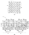
本発明の各実施形態を述べるに先立って、図1を参照しながら、固体撮像装置IDを参考例として説明する。固体撮像装置IDは、1つの基板101(半導体基板)に配列された撮像用の画素10(赤色画素10R、緑色画素10G及び青色画素10Bを含む)と、焦点検出用の画素(AF用の画素)11AFとを有する。図1(a)に例示されるように、赤色画素10R、緑色画素10G及び青色画素10Bのそれぞれは、ベイヤ配列にしたがって配列されており、また、AF用の画素11AFが、青色画素10Bが配されるべき位置の一部に配されている。固体撮像装置IDにおいて、領域R1は青色画素10Bと緑色画素10Gとが隣接する領域であり、領域R2はAF用の画素11AFと緑色画素10Gとが隣接する領域である。
Prior to describing each embodiment of the present invention, a solid-state imaging device ID will be described as a reference example with reference to FIG. The solid-state imaging device ID includes imaging pixels 10 (including
図1(b)は、固体撮像装置IDのうち、領域R1及び領域R2のそれぞれの断面構造を模式的に示している。撮像用の画素10及びAF用の画素11AFのそれぞれには、基板101の上に、層間絶縁層110等、コンタクトプラグ111等、配線パターン112等、パッシベーション膜130、マイクロレンズ135が設けられている。また、撮像用の画素10には、対応する色のカラーフィルタ134(134R、134G又は134B)が、光電変換部102とマイクロレンズ135との間のフィルタ層132に配されうる。例えば、緑色画素10G(第1画素)には、緑色光(第1波長の光)を通過させるカラーフィルタ134G(第1カラーフィルタ)が配される。例えば、青色画素10B(第2画素)では、青色光(第2波長の光)を通過させるカラーフィルタ134B(第2カラーフィルタ)が配される。例えば、赤色画素10R(第3画素)では、赤色光(第3波長の光)を通過させるカラーフィルタ134R(第3カラーフィルタ)が配される。なお、配線パターン112等は、配線層M1〜M3を構成する。
FIG. 1B schematically shows a cross-sectional structure of each of the regions R1 and R2 in the solid-state imaging device ID . Each of the
AF用の画素11AFでは焦点検出を行うのに十分な信号が得られればよく、AF用の画素11AFにはカラーフィルタ134が設けられなくてもよい。ここでは、AF用の画素11AFには光透過性を有する無色の部材133が設けられた構造を例示したが、この構造に限定されない。例えば、AF用の画素11AFは、カラーフィルタ134や部材133が配されない構造を採ってもよい。
The
撮像用の画素10及びAF用の画素11AFのそれぞれは公知の回路構成を採ればよく、光電変換部102の他、光電変換部102から電気信号を読み出すための複数のトランジスタ、例えば転送トランジスタ及びソースフォロワトランジスタを含みうる。転送トランジスタのゲートに与えられる制御信号が活性化されると、光電変換部102において発生し蓄積された信号電荷(以下、電荷)が、転送トランジスタによってソースフォロワトランジスタのゲートに転送されうる。これにより、当該ゲートの電位が変化し、当該電位の変化に応じてソースフォロワトランジスタに流れる電流量が変化しうる。なお、図1(b)では、転送トランジスタのゲート電極104と、転送トランジスタの一方の拡散領域であるフローティングディフュージョン105(FD105)とを代表して図示している。FD105は、上述のソースフォロワトランジスタのゲートに電気的に接続される。
Each of the
また、各撮像用の画素10(又はAF用の画素11AF)は、複数のトランジスタとして、例えば選択トランジスタをさらに含みうる。選択トランジスタのゲートに与えられる制御信号が活性化されると、選択トランジスタは、ソースフォロワトランジスタの電流量に応じた信号を出力しうる。その他、各撮像用の画素10(又はAF用の画素11AF)は、複数のトランジスタとして、例えばリセットトランジスタをさらに含みうる。リセットトランジスタのゲートに与えられる制御信号が活性化されると、リセットトランジスタはソースフォロワトランジスタのゲートの電位をリセットしうる。なお、図1(b)に示すように、各画素は同一の回路構成を有しうる。 Each imaging pixel 10 (or AF pixel 11 AF ) may further include, for example, a selection transistor as a plurality of transistors. When the control signal applied to the gate of the selection transistor is activated, the selection transistor can output a signal corresponding to the amount of current of the source follower transistor. In addition, each imaging pixel 10 (or AF pixel 11 AF ) may further include, for example, a reset transistor as a plurality of transistors. When the control signal applied to the gate of the reset transistor is activated, the reset transistor can reset the potential of the gate of the source follower transistor. As shown in FIG. 1B, each pixel can have the same circuit configuration.
以上のような構成により、各撮像用の画素10(又はAF用の画素11AF)から信号がそれぞれ読み出されうる。各撮像用の画素10から読み出された信号は、例えば画像処理等の信号処理を行う処理部(不図示)に入力され、画像データが形成されうる。また、焦点検出は、例えば位相差検出方式によって為され、AF用の画素11AFは、瞳分割を行うように、例えば配線層M1〜M3のいずれか(ここでは配線層M1)に、開口OPAFを有する遮光パターン113が設けられた構造を採りうる。開口OPAFは、光電変換部102の中心から偏心されるように設けられ、遮光パターン113は光電変換部102に入射する光を制限する。この構成によって各AF用の画素11AFから読み出された信号が、例えば焦点検出を行う焦点検出部(不図示)に入力され、焦点検出の結果に応じてレンズ位置が調整されうる。
With the configuration as described above, signals can be read out from the respective imaging pixels 10 (or AF pixels 11 AF ). A signal read from each
ここで、基板101上には、各画素の光電変換部の間に、絶縁体からなる素子分離部103が設けられる。また、基板101には、各画素の光電変換部で生じた電荷の隣接画素間での移動により生じるクロストークを防ぐように各画素の間に素子分離領域106が設けられうる。この画素の間の素子分離部103および画素の間の素子分離領域106とは、光電変換部とその隣の光電変換部との間の素子分離部103と素子分離領域106と言える。更に、素子分離領域106は、各画素の光電変換部102の外周を取り囲むように配されうる。しかし、高画素化(画素の小サイズ化)に伴って、素子分離部103、素子分離領域106、あるいはそれら両方も小さくなるため、クロストークを抑制することが困難になる。クロストークとは、隣接画素に信号電荷が混入することであり、クロストークの量とは、隣接画素に混入する信号電荷量を意味する。本構成において、このクロストーク量は、青色画素10Bと緑色画素10Gとの間と、AF用の画素11AFと緑色画素10Gとの間とで大きさが異なりうる。これは、光が基板101の表面から侵入する長さが当該光の波長によって異なり、例えば、AF用の画素11AFの光電変換部102に入射した光が、青色光よりも基板101の表面から深い位置で光電変換が為されて電荷が生じることに起因する。よって、図1(b)の矢印で例示されるように、AF用の画素11AFに隣接する緑色画素10Gへ移動する電荷の量は、青色画素10Bに隣接する緑色画素10Gへ移動する電荷の量よりも多くなる。その結果、領域R1と領域R2とではクロストークの量が異なるため、固体撮像装置IDにより得られる画像の品質が低下しうる。なお、本説明では、信号電荷が電子の場合を例に説明を行っている。
Here, an
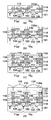
(第1実施形態)
図2及び図3を参照しながら、第1実施形態の固体撮像装置I1を説明する。図2は、固体撮像装置I1の断面構造を図1(b)と同様にして示している。固体撮像装置I1では、AF用の画素11AF/緑色画素10G間において、青色画素10B/緑色画素10G間の素子分離領域106(第2領域)よりも深さが深い素子分離領域107(第1領域)が基板101に形成されている。素子分離領域107は、素子分離領域106より深さが深いため、電荷の移動(例えば拡散による移動)を妨げる能力が素子分離領域106よりも高い。
(First embodiment)
With reference to FIGS. 2 and 3, illustrating a solid-state imaging device I 1 of the first embodiment. FIG. 2 shows the cross-sectional structure of the solid-state imaging device I 1 in the same manner as FIG. In the solid-state imaging device I 1, between pixels 11 AF /
当該構造によると、AF用の画素11AF/緑色画素10G間の素子分離領域107が、青色画素10B/緑色画素10G間の素子分離領域106よりも深く形成されており、AF用の画素11AFに隣接する緑色画素10Gに流入する電荷量が抑制される。その結果、AF用の画素11AF/緑色画素10G間のクロストークの量と、青色画素10B/緑色画素10G間のクロストークの量との差を小さくすることできる。即ち、AF用の画素11AFに隣接する緑色画素10Gへ移動する電荷の量と、青色画素10Bに隣接する緑色画素10Gへ移動する電荷の量との差が均一化されうる。
According to this structure, the
よって、固体撮像装置I1によると、撮像用の画素10とAF用の画素11AFとが1つの基板101に配列された構成において、AF用の画素11AFが配された領域と、それ以外の領域とでクロストークの量の差が小さくなるよう均一化される。これにより、取得される画像の品質が向上しうる。また、このことは、AF用の画素11AFが配線層M1〜M3のうちの配線層M1に遮光パターン113が設けられた構造を採ることによってAF用の画素11AFへの入射光量が大きくなる場合にも有利である。
Therefore, according to the solid-state imaging device I 1 , in the configuration in which the
本実施形態では、素子分離領域107による電荷の移動を妨げる能力が素子分離領域106よりも高い構造の例として、素子分離領域107が素子分離領域106より深さが深いものを例示した。しかし、素子分離領域107が、素子分離領域106よりも電荷の移動を妨げる能力が高くなるように形成されればよく、本発明は上述の構造に限定されない。例えば、素子分離領域107が素子分離領域106よりも幅(分離される画素間方向の幅)が広い構造でもよいし、素子分離領域107が素子分離領域106よりも不純物濃度が高い構造でもよい。また、それらを組み合わせた構造でもよい。
In this embodiment, as an example of the structure in which the ability to prevent the movement of electric charges by the
なお、電荷の移動を妨げる能力が高いとは、信号電荷に対する障壁が高いということである。ここで、障壁とは、例えば、ポテンシャル障壁である。また、素子分離領域106〜107による障壁のみならず、素子分離部103の構造(深さ、幅)を変えて(深さを深くして、又は幅を広くして)、高い障壁を形成してもよい。
Note that the high ability to prevent the movement of charges means that the barrier against signal charges is high. Here, the barrier is, for example, a potential barrier. Further, not only the barrier by the
以下では、図3を参照しながら、固体撮像素子I1の製造方法を述べる。ここでは領域R2について図示している。まず、図3(a)に示されるように、例えばP型シリコン等の半導体領域を有する基板101が用意され、基板101の表面には例えばLOCOS法等によって素子分離部103が形成されうる。
Hereinafter, with reference to FIG. 3, it described a method for manufacturing the solid-state imaging device I 1. Here, the region R2 is illustrated. First, as shown in FIG. 3A, a
次に、基板101の上にフォトレジストパターンを形成した後に、例えばイオン注入法によって素子分離部103の下にP型の不純物を注入し、素子分離領域106及び素子分離領域107が形成されうる。ここで、互いに深さが異なる素子分離領域106及び107の形成は、例えば、互いに残膜の膜厚が異なる2種類の開口を有するフォトレジストパターンを形成した後に不純物注入を行うことによって為されてもよい。また、素子分離領域106の形成と素子分離領域107の形成とは、それぞれに対応するフォトレジストパターンと不純物注入とを個別に順に行うことによって、それぞれ為されてもよい。また、素子分離領域106と素子分離領域107となる部分に、素子分離領域106を形成するための不純物注入を行った後に、素子分離領域107となる部分に、追加の不純物注入を行ってもよい。また、前述の素子分離領域107の幅が広い構造を形成する場合は、例えばフォトレジストパターンの開口の幅を調節すればよいし、素子分離領域107の不純物濃度が高い構造を形成する場合は、例えば不純物注入量を調節すればよい。
Next, after a photoresist pattern is formed on the
その後、各種トランジスタ(転送トランジスタ、ソースフォロワトランジスタ等)のゲート電極(ここではゲート電極104)やN型の拡散領域(ここでは光電変換部102及びFD105)が、公知の半導体プロセスを用いて形成されうる。図3(a)には図示していないが、基板101の表面には、各トランジスタのゲート絶縁膜や自然酸化膜が形成されうる。
Thereafter, gate electrodes (here, the gate electrode 104) and N-type diffusion regions (here, the
次に、例えばCVD(気相成長)法等によって、酸化シリコン又はこれを主成分とする絶縁性の材料で構成された第1の層間絶縁膜110が、ゲート電極104等を覆うように基板101の上に形成される。その後、例えばCMP(化学的機械的研磨)法等によって層間絶縁膜110の上面が平坦化される。次に、第1配線層M1に形成されるべき配線パターン112と、基板101やゲート電極等とを接続するコンタクトプラグ111が形成される。次に、例えばAl、Mo、W、Ta、Ti、TiN若しくはCu、若しくはこれらを主成分とする金属膜、又はこれらの積層膜が、スパッタリング、CVD法又は電解メッキ法等によって層間絶縁膜110の上に形成される。その後、リソグラフィ工程及びエッチング工程を経て、配線パターン112及び遮光パターン113が第1配線層M1に形成されうる。次に、層間絶縁膜110と同様の手順で、第2の層間絶縁膜114が、配線パターン112及び遮光パターン113を覆うように第1配線層M1の上に形成される。第2の層間絶縁膜114の上面はCMP法等によって平坦化されうる。その後、第1配線層M1の配線パターン112と、後に形成される第2配線層M2に含まれる配線パターン116とを接続するコンタクトプラグ115のための開口115aが形成されうる。
Next, the
次に、図3(b)に示されるように、例えばAl、Mo、W、Ta、Ti、TiN若しくはCu、若しくはこれらを主成分とする金属部材が、スパッタリング、CVD法又は電解メッキ法等によって開口115aに形成される。さらに、この金属部材はCMP法やエッチバック法等によって平坦化され、コンタクトプラグ115が形成される。次に、配線パターン112及び遮光パターン113と同様の手順で、配線パターン116が第2配線層M2に形成される。さらに、層間絶縁膜114と同様の手順で、第3の層間絶縁層117が、配線パターン116を覆うように第2配線層M2の上に形成され、その上面がCMP法等によって平坦化される。その後、コンタクトプラグ115と同様の手順で、第3配線層M3に形成されるべき配線パターン119と第2配線層M2の配線パターン116とを接続するコンタクトプラグ118のための開口118aが形成される。
Next, as shown in FIG. 3B, for example, Al, Mo, W, Ta, Ti, TiN or Cu, or a metal member mainly composed of these is formed by sputtering, CVD, electrolytic plating, or the like. An
次に、図3(c)に示されるように、開口115aないしコンタクトプラグ115と同様の手順で、層間絶縁層117に開口118aが形成され、その後、コンタクトプラグ118が形成される。さらに、配線パターン116と同様の手順で、配線パターン119が第3配線層M3に形成されうる。その後、配線パターン119を覆うように、無機材料からなるパッシベーション膜130が層間絶縁膜117の上に形成される。
Next, as shown in FIG. 3C, an
次に、図3(d)に示されるように、例えば塗布法によって、有機材料からなる平坦化層131が、パッシベーション膜130の上に形成されうる。その後、フィルタ層132が平坦化層131の上に形成され、各撮像用の画素10又はAF用の画素11AFに対応してカラーフィルタ134又は光透過性を有する無色の部材133が設けられる。最後に、フィルタ層132の上に形成される平坦化層(不図示)の上に、所定のパターニング及びリフロー処理を経て、マイクロレンズ135が各撮像用の画素10又はAF用の画素11AFに対応して形成されうる。ここで、無色の部材133は、フィルタ層132の上に形成される平坦化層と一体の部材であってもよい。
Next, as shown in FIG. 3D, a
以上の製造方法により、撮像用の画素10とAF用の画素11AFとが1つの基板101に配列された構成から得られる画像の高品質化に有利な固体撮像装置I1が得られる。
With the above manufacturing method, the solid-state imaging device I 1 that is advantageous for improving the quality of an image obtained from a configuration in which the
(第2実施形態)
図4及び図5を参照しながら、第2実施形態の固体撮像装置I2を説明する。本実施形態は、AF用の画素11AFの他、第2の焦点検出用の画素12AFが、赤色画素10Rが配されるべき位置の一部にさらに配されている点で第1実施形態と異なる。図4は、固体撮像装置I2の断面構造を模式的に示している。
(Second Embodiment)
The solid-state imaging device I 2 of the second embodiment will be described with reference to FIGS. 4 and 5. In the present embodiment, in addition to the AF
AF用の画素12AFは、AF用の画素11AFと同様に、例えば配線層M1に開口OPAFを有する遮光パターン113が配された構造であるため、AF用の画素12AFへの入射光量が少なくなりうる。よって、AF用の画素12AFにおいて発生する電荷の量は、赤色画素10Rにおいて発生する電荷の量よりも少なくなる。隣接画素へ移動する電荷の量は、発生した電荷量に依存するため、AF用の画素12AFに隣接する緑色画素10Gへ移動する電荷の量は、赤色画素10Rに隣接する緑色画素10Gへ移動する電荷の量よりも少なくなる。即ち、撮像用の画素10とAF用の画素12AFとが1つの基板101に配列された構成において、AF用の画素12AFが配された領域と、それ以外の領域とでクロストークの量が大きく異なってしまう。
Like the AF
そこで、固体撮像装置I2では、AF用の画素12AFとその隣接画素10との間に形成されるべき素子分離領域108(第3領域)は、第1実施形態で述べた素子分離領域106よりも電荷の移動を妨げる能力が小さくなるように設けられる。素子分離領域108は、例えば、図5(図3(a)に対応)に示されるように、素子分離領域106より深さが浅くなるように形成されうる。すなわち、素子分離領域106〜108のそれぞれは、素子分離領域107、素子分離領域106、素子分離領域108の順に、基板101の表面からの深さが深くなるように、それぞれ形成されうる。
Therefore, in the solid-state imaging device I 2, the
また、素子分離領域108の他の構成としては、例えば、素子分離領域108は、素子分離領域106よりも幅(分離される画素間方向の幅)が狭い構造を採ってもよいし、素子分離領域108が素子分離領域106よりも不純物濃度が低い構造を採ってもよい。また、それらを組み合わせた構造でもよい。
In addition, as another configuration of the
その後、第1実施形態と同様の手順で、層間絶縁層110等、コンタクトプラグ111等、遮光パターン113、配線パターン112等、パッシベーション膜130、フィルタ層132、マイクロレンズ135が、適宜、順に形成されうる。
Thereafter, the
当該構造によると、第1実施形態で述べた効果に加え、AF用の画素12AF/緑色画素10G間のクロストークの量と、赤色画素10R/緑色画素10G間のクロストークの量の差が小さくなる。即ち、AF用の画素12AFに隣接する緑色画素10Gへ移動する電荷の量と、赤色画素10Rに隣接する緑色画素10Gへ移動する電荷の量との差が小さくなる。
According to this structure, in addition to the effects described in the first embodiment, the amount of crosstalk between the AF
よって、固体撮像装置I2によると、第2のAF用の画素12AFがさらに基板101に配列された構成において、AF用の画素12AFが配された領域と、それ以外の領域とでクロストークの量の差が小さくなり、取得される画像の品質が向上する。なお、AF用の画素は、AF用の画素11AFを含まず、第2のAF用の画素12AFで構成されていてもよい。この場合にも、クロストークの量の差を低減することが可能である。
Therefore, according to the solid-state imaging device I 2 , in the configuration in which the
以上の2つの実施形態を述べたが、本願発明はこれらに限られるものではなく、目的、状態、用途及び機能その他の仕様に応じて、適宜、変更が可能であり、他の実施形態によっても為されうる。例えば、上述の各実施形態では、複数の画素がベイヤ配列にしたがって配列された構成を例示したが、本願発明は当該構成に限られるものではなく、複数の画素は、例えばハニカム配列等の他の構成を採ってもよい。 Although the above two embodiments have been described, the present invention is not limited to these embodiments, and can be appropriately changed according to the purpose, state, application, function, and other specifications. Can be done. For example, in each of the above-described embodiments, the configuration in which a plurality of pixels are arranged according to the Bayer array is illustrated. However, the present invention is not limited to this configuration, and the plurality of pixels may be other types such as a honeycomb array. A configuration may be adopted.
(撮像システム)
また、以上の実施形態は、カメラ等に代表される撮像システムに含まれる固体撮像装置について述べた。撮像システムの概念には、撮影を主目的とする装置のみならず、撮影機能を補助的に備える装置(例えば、パーソナルコンピュータ、携帯端末)も含まれる。撮像システムは、上記の実施形態として例示された本発明に係る固体撮像装置と、当該固体撮像装置から出力される信号を処理する処理部とを含みうる。焦点検出のための信号処理は当該処理部によって為されてもよい。また、当該処理部は、例えば、A/D変換器及び当該A/D変換器から出力されるデジタルデータを処理するプロセッサを含みうる。
(Imaging system)
Moreover, the above embodiment described the solid-state imaging device contained in the imaging system represented by the camera etc. The concept of the imaging system includes not only a device mainly for photographing, but also a device (for example, a personal computer or a portable terminal) that is supplementarily provided with a photographing function. The imaging system may include the solid-state imaging device according to the present invention exemplified as the above-described embodiment, and a processing unit that processes a signal output from the solid-state imaging device. Signal processing for focus detection may be performed by the processing unit. The processing unit may include, for example, an A / D converter and a processor that processes digital data output from the A / D converter.
Claims (8)
前記基板において、前記複数の画素のそれぞれの間に形成された素子分離領域を備え、
前記複数の画素は、
第1波長の光を通過させるための第1カラーフィルタが設けられた第1画素と、
前記第1波長より短い第2波長の光を通過させるための第2カラーフィルタが設けられた第2画素と、
前記第1波長より長い第3波長の光を通過させるための第3カラーフィルタが設けられた第3画素と、
前記光電変換部に対して偏心する開口が設けられた第1の遮光パターンを有する画素であって、前記第2波長より長い光が該開口を介して前記光電変換部に入射するように構成された第1の遮光パターンを有する画素と、
前記光電変換部に対して偏心する開口が設けられた第2の遮光パターンを有する画素であって、前記第2波長より長い光が該開口を介して前記光電変換部に入射するように構成された第2の遮光パターンを有する画素と、
を含んでおり、
前記第1画素はベイヤ配列における緑色画素に対応する位置に配され、前記第1の遮光パターンを有する画素又は前記第2画素は前記ベイヤ配列における青色画素に対応する位置に配され、前記第2の遮光パターンを有する画素又は前記第3画素は前記ベイヤ配列における赤色画素に対応する位置に配されており、
前記素子分離領域のうち、前記第1の遮光パターンを有する画素と前記第1画素との間の第1領域は、前記第1画素と前記第2画素との間の第2領域よりも、信号電荷に対して高い障壁を有し、
前記素子分離領域のうち、前記第2の遮光パターンを有する画素と前記第1画素との間の第3領域は、前記第2領域よりも、信号電荷に対して低い障壁を有する、
ことを特徴とする固体撮像装置。 A solid-state imaging device including a plurality of pixels each having a photoelectric conversion unit arranged on a substrate,
In the substrate, comprising an element isolation region formed between each of the plurality of pixels,
The plurality of pixels are:
A first pixel provided with a first color filter for passing light of a first wavelength;
A second pixel provided with a second color filter for passing light having a second wavelength shorter than the first wavelength;
A third pixel provided with a third color filter for passing light having a third wavelength longer than the first wavelength;
A pixel having a first light-shielding pattern having an opening eccentrically with respect to the photoelectric conversion unit is provided, the longer the light from the second wavelength is configured to be incident on the photoelectric conversion portion via the opening A pixel having a first light-shielding pattern;
A pixel having a second light-shielding pattern provided with an opening that is eccentric with respect to the photoelectric conversion unit, and is configured such that light having a wavelength longer than the second wavelength is incident on the photoelectric conversion unit through the opening. A pixel having a second light-shielding pattern;
Contains
The first pixel is disposed at a position corresponding to a green pixel in the Bayer array, the pixel having the first light shielding pattern or the second pixel is disposed at a position corresponding to a blue pixel in the Bayer array, and the second pixel The pixel having the light shielding pattern or the third pixel is disposed at a position corresponding to the red pixel in the Bayer array,
In the element isolation region, the first region between the pixel having the first light-shielding pattern and the first pixel is more signal than the second region between the first pixel and the second pixel. have a high barrier to the charge,
Part of the device isolation region, a third region between the pixel and the first pixel with the second light-shielding pattern, the than the second region, to have a low barrier to the signal charges,
A solid-state imaging device.
前記第1領域は、前記第2領域よりも前記基板からの深さが深い、
前記第1領域は、前記第2領域よりも不純物濃度が高い、ことの少なくともいずれか1つをみたす、
ことを特徴とする請求項1に記載の固体撮像装置。 The first region is wider in the inter-pixel direction than the second region.
The first region is deeper from the substrate than the second region;
The first region satisfies at least one of the fact that the impurity concentration is higher than that of the second region.
The solid-state imaging device according to claim 1.
前記第1画素はベイヤ配列における緑色画素に対応する位置に配され、前記第1の遮光パターンを有する画素又は前記第2画素は前記ベイヤ配列における青色画素に対応する位置に配され、前記第3画素は前記ベイヤ配列における赤色画素に対応する位置に配されている、
ことを特徴とする請求項1又は2に記載の固体撮像装置。 The plurality of pixels further include a third pixel provided with a third color filter for passing light having a third wavelength longer than the first wavelength.
The first pixel is disposed at a position corresponding to a green pixel in the Bayer array, the pixel having the first light shielding pattern or the second pixel is disposed at a position corresponding to a blue pixel in the Bayer array, and the third pixel Pixels are arranged at positions corresponding to red pixels in the Bayer array,
The solid-state imaging device according to claim 1 or 2.
前記第1の遮光パターンは、前記複数の配線層のうち前記基板に最も近い側の配線層に配されている、
ことを特徴とする請求項1乃至3のいずれか1項に記載の固体撮像装置。 The plurality of pixels further includes a plurality of wiring layers,
The first light shielding pattern is disposed on a wiring layer closest to the substrate among the plurality of wiring layers.
The solid-state imaging device according to any one of claims 1 to 3.
前記第3領域は、前記第2領域よりも前記基板からの深さが浅い、
前記第3領域は、前記第2領域よりも不純物濃度が低い、ことの少なくともいずれか1つをみたす、
ことを特徴とする請求項1乃至4のいずれか1項に記載の固体撮像装置。 The third region is narrower in the inter-pixel direction than the second region,
The third region is shallower from the substrate than the second region,
The third region satisfies at least one of the following: the impurity concentration is lower than that of the second region;
The solid-state imaging device according to claim 1 , wherein the solid-state imaging device is provided.
前記第1の遮光パターンは、前記複数の配線層のうち前記基板に最も近い側の配線層に配されている、
ことを特徴とする請求項1乃至5のいずれか1項に記載の固体撮像装置。 The plurality of pixels further includes a plurality of wiring layers,
The first light shielding pattern is disposed on a wiring layer closest to the substrate among the plurality of wiring layers.
The solid-state imaging device according to claim 1 , wherein the solid-state imaging device is provided.
ことを特徴とする請求項1乃至6のいずれか1項に記載の固体撮像装置。 On the element isolation region, the solid-state imaging device according to any one of claims 1 to 6, characterized in that the element isolation portion made of an insulator is provided.
前記固体撮像装置から出力される信号を処理する処理部と、
を備えることを特徴とする撮像システム。
A solid-state imaging device according to any one of claims 1 to 7 ,
A processing unit for processing a signal output from the solid-state imaging device;
An imaging system comprising:
Priority Applications (2)
| Application Number | Priority Date | Filing Date | Title |
|---|---|---|---|
| JP2013059060A JP6141065B2 (en) | 2013-03-21 | 2013-03-21 | Solid-state imaging device and imaging system |
| US14/205,801 US9086577B2 (en) | 2013-03-21 | 2014-03-12 | Solid-state imaging apparatus and imaging system |
Applications Claiming Priority (1)
| Application Number | Priority Date | Filing Date | Title |
|---|---|---|---|
| JP2013059060A JP6141065B2 (en) | 2013-03-21 | 2013-03-21 | Solid-state imaging device and imaging system |
Publications (3)
| Publication Number | Publication Date |
|---|---|
| JP2014187067A JP2014187067A (en) | 2014-10-02 |
| JP2014187067A5 JP2014187067A5 (en) | 2016-05-12 |
| JP6141065B2 true JP6141065B2 (en) | 2017-06-07 |
Family
ID=51568891
Family Applications (1)
| Application Number | Title | Priority Date | Filing Date |
|---|---|---|---|
| JP2013059060A Expired - Fee Related JP6141065B2 (en) | 2013-03-21 | 2013-03-21 | Solid-state imaging device and imaging system |
Country Status (2)
| Country | Link |
|---|---|
| US (1) | US9086577B2 (en) |
| JP (1) | JP6141065B2 (en) |
Families Citing this family (4)
| Publication number | Priority date | Publication date | Assignee | Title |
|---|---|---|---|---|
| JP6087681B2 (en) * | 2013-03-21 | 2017-03-01 | キヤノン株式会社 | Solid-state imaging device and imaging system |
| JP6104049B2 (en) * | 2013-05-21 | 2017-03-29 | オリンパス株式会社 | Image processing apparatus, image processing method, and image processing program |
| CN105810697B (en) * | 2014-12-31 | 2018-06-29 | 格科微电子(上海)有限公司 | Imaging sensor and its color recognition method |
| JP6941011B2 (en) | 2017-09-04 | 2021-09-29 | キヤノン株式会社 | Imaging device and its control method, program, storage medium |
Family Cites Families (10)
| Publication number | Priority date | Publication date | Assignee | Title |
|---|---|---|---|---|
| JP5023480B2 (en) | 2005-12-02 | 2012-09-12 | 株式会社ニコン | Electronic camera |
| JP4839990B2 (en) | 2006-07-06 | 2011-12-21 | 株式会社ニコン | Solid-state imaging device and imaging apparatus using the same |
| JP5045012B2 (en) | 2006-07-20 | 2012-10-10 | 株式会社ニコン | Solid-state imaging device and imaging apparatus using the same |
| JP2008270298A (en) * | 2007-04-16 | 2008-11-06 | Nikon Corp | Solid-state image sensor and imaging apparatus employing the same |
| JP5364995B2 (en) | 2007-10-01 | 2013-12-11 | 株式会社ニコン | Solid-state imaging device and electronic camera using the same |
| JP5558857B2 (en) * | 2009-03-09 | 2014-07-23 | キヤノン株式会社 | Photoelectric conversion device and imaging system using the same |
| JP5414358B2 (en) * | 2009-05-20 | 2014-02-12 | キヤノン株式会社 | Imaging device |
| JP2012004264A (en) | 2010-06-16 | 2012-01-05 | Fujifilm Corp | Solid-state imaging element and imaging device |
| JP5693082B2 (en) | 2010-08-09 | 2015-04-01 | キヤノン株式会社 | Imaging device |
| JP5814626B2 (en) * | 2011-05-27 | 2015-11-17 | キヤノン株式会社 | Photoelectric conversion device and method of manufacturing photoelectric conversion device |
-
2013
- 2013-03-21 JP JP2013059060A patent/JP6141065B2/en not_active Expired - Fee Related
-
2014
- 2014-03-12 US US14/205,801 patent/US9086577B2/en not_active Expired - Fee Related
Also Published As
| Publication number | Publication date |
|---|---|
| JP2014187067A (en) | 2014-10-02 |
| US20140285701A1 (en) | 2014-09-25 |
| US9086577B2 (en) | 2015-07-21 |
Similar Documents
| Publication | Publication Date | Title |
|---|---|---|
| US11843015B2 (en) | Image sensors | |
| KR102214822B1 (en) | Solid-state imaging device, method of manufacturing the same, and electronic apparatus | |
| US7537951B2 (en) | Image sensor including spatially different active and dark pixel interconnect patterns | |
| US20170170230A1 (en) | Image capturing apparatus, manufacturing method thereof, and camera | |
| JP5468133B2 (en) | Solid-state imaging device | |
| JP5814626B2 (en) | Photoelectric conversion device and method of manufacturing photoelectric conversion device | |
| JP2009021415A (en) | Solid-state imaging apparatus and manufacturing method thereof | |
| JP6148530B2 (en) | Solid-state imaging device and camera | |
| JP6021439B2 (en) | Solid-state imaging device | |
| US11177309B2 (en) | Image sensor with pad structure | |
| JP6141065B2 (en) | Solid-state imaging device and imaging system | |
| JP5037922B2 (en) | Solid-state imaging device | |
| JP6087681B2 (en) | Solid-state imaging device and imaging system | |
| JP2014086514A (en) | Solid state imaging device, method for manufacturing the same, and camera | |
| JP4535766B2 (en) | Solid-state imaging device, manufacturing method thereof, and electronic information device | |
| JP2006344914A (en) | Solid-state imaging apparatus, its manufacturing method, and camera | |
| JP2005277404A (en) | Solid-state imaging device and method of manufacturing solid-state imaging device | |
| JP2014086515A (en) | Solid state imaging device, method for manufacturing the same, and camera | |
| WO2011155182A1 (en) | Solid-state imaging element | |
| JP5035452B2 (en) | Solid-state imaging device | |
| KR20110068679A (en) | Image sensor and method for manufacturing thereof | |
| TW201030959A (en) | Solid-state imaging device, imaging apparatus, and manufacturing method of solid-state imaging device | |
| JP2007208139A (en) | Solid-state imaging element and manufacturing method therefor |
Legal Events
| Date | Code | Title | Description |
|---|---|---|---|
| A521 | Request for written amendment filed |
Free format text: JAPANESE INTERMEDIATE CODE: A523 Effective date: 20160317 |
|
| A621 | Written request for application examination |
Free format text: JAPANESE INTERMEDIATE CODE: A621 Effective date: 20160317 |
|
| A131 | Notification of reasons for refusal |
Free format text: JAPANESE INTERMEDIATE CODE: A131 Effective date: 20161222 |
|
| A977 | Report on retrieval |
Free format text: JAPANESE INTERMEDIATE CODE: A971007 Effective date: 20161222 |
|
| A521 | Request for written amendment filed |
Free format text: JAPANESE INTERMEDIATE CODE: A523 Effective date: 20170215 |
|
| TRDD | Decision of grant or rejection written | ||
| A01 | Written decision to grant a patent or to grant a registration (utility model) |
Free format text: JAPANESE INTERMEDIATE CODE: A01 Effective date: 20170407 |
|
| A61 | First payment of annual fees (during grant procedure) |
Free format text: JAPANESE INTERMEDIATE CODE: A61 Effective date: 20170502 |
|
| R151 | Written notification of patent or utility model registration |
Ref document number: 6141065 Country of ref document: JP Free format text: JAPANESE INTERMEDIATE CODE: R151 |
|
| LAPS | Cancellation because of no payment of annual fees |