JP6132425B2 - Method for equalizing electrode height of wiring board and method for manufacturing wiring board using the same - Google Patents
Method for equalizing electrode height of wiring board and method for manufacturing wiring board using the same Download PDFInfo
- Publication number
- JP6132425B2 JP6132425B2 JP2013038487A JP2013038487A JP6132425B2 JP 6132425 B2 JP6132425 B2 JP 6132425B2 JP 2013038487 A JP2013038487 A JP 2013038487A JP 2013038487 A JP2013038487 A JP 2013038487A JP 6132425 B2 JP6132425 B2 JP 6132425B2
- Authority
- JP
- Japan
- Prior art keywords
- wiring board
- wiring
- electrode
- height
- substrate
- Prior art date
- Legal status (The legal status is an assumption and is not a legal conclusion. Google has not performed a legal analysis and makes no representation as to the accuracy of the status listed.)
- Expired - Fee Related
Links
- 238000000034 method Methods 0.000 title claims description 45
- 238000004519 manufacturing process Methods 0.000 title claims description 7
- 239000000758 substrate Substances 0.000 claims description 68
- 239000002184 metal Substances 0.000 claims description 51
- 229910052751 metal Inorganic materials 0.000 claims description 51
- 230000003014 reinforcing effect Effects 0.000 claims description 45
- 239000012790 adhesive layer Substances 0.000 claims description 38
- 239000010410 layer Substances 0.000 claims description 38
- 238000005498 polishing Methods 0.000 claims description 34
- 238000011049 filling Methods 0.000 claims description 12
- 230000002093 peripheral effect Effects 0.000 claims description 6
- 239000000523 sample Substances 0.000 claims description 5
- 230000002787 reinforcement Effects 0.000 claims description 4
- 239000004840 adhesive resin Substances 0.000 claims description 2
- 229920006223 adhesive resin Polymers 0.000 claims description 2
- 239000000470 constituent Substances 0.000 claims 1
- 238000009499 grossing Methods 0.000 claims 1
- 239000000463 material Substances 0.000 description 9
- 239000000126 substance Substances 0.000 description 6
- PXHVJJICTQNCMI-UHFFFAOYSA-N Nickel Chemical compound [Ni] PXHVJJICTQNCMI-UHFFFAOYSA-N 0.000 description 4
- 238000007747 plating Methods 0.000 description 4
- 239000004065 semiconductor Substances 0.000 description 4
- 238000000227 grinding Methods 0.000 description 3
- RYGMFSIKBFXOCR-UHFFFAOYSA-N Copper Chemical compound [Cu] RYGMFSIKBFXOCR-UHFFFAOYSA-N 0.000 description 2
- 229910000881 Cu alloy Inorganic materials 0.000 description 2
- XEEYBQQBJWHFJM-UHFFFAOYSA-N Iron Chemical compound [Fe] XEEYBQQBJWHFJM-UHFFFAOYSA-N 0.000 description 2
- 229910000990 Ni alloy Inorganic materials 0.000 description 2
- 239000003795 chemical substances by application Substances 0.000 description 2
- 229910052802 copper Inorganic materials 0.000 description 2
- 239000010949 copper Substances 0.000 description 2
- 238000005260 corrosion Methods 0.000 description 2
- 230000007797 corrosion Effects 0.000 description 2
- 238000007689 inspection Methods 0.000 description 2
- 229910052759 nickel Inorganic materials 0.000 description 2
- 229920001225 polyester resin Polymers 0.000 description 2
- 239000004645 polyester resin Substances 0.000 description 2
- 239000011347 resin Substances 0.000 description 2
- 229920005989 resin Polymers 0.000 description 2
- ATJFFYVFTNAWJD-UHFFFAOYSA-N Tin Chemical compound [Sn] ATJFFYVFTNAWJD-UHFFFAOYSA-N 0.000 description 1
- 239000000853 adhesive Substances 0.000 description 1
- 230000001070 adhesive effect Effects 0.000 description 1
- 230000002411 adverse Effects 0.000 description 1
- 238000005452 bending Methods 0.000 description 1
- 230000015572 biosynthetic process Effects 0.000 description 1
- 239000000919 ceramic Substances 0.000 description 1
- 239000004020 conductor Substances 0.000 description 1
- 238000001723 curing Methods 0.000 description 1
- 238000005520 cutting process Methods 0.000 description 1
- 238000000151 deposition Methods 0.000 description 1
- 230000018109 developmental process Effects 0.000 description 1
- 238000001035 drying Methods 0.000 description 1
- 230000000694 effects Effects 0.000 description 1
- 238000005530 etching Methods 0.000 description 1
- 239000000835 fiber Substances 0.000 description 1
- 239000011521 glass Substances 0.000 description 1
- PCHJSUWPFVWCPO-UHFFFAOYSA-N gold Chemical compound [Au] PCHJSUWPFVWCPO-UHFFFAOYSA-N 0.000 description 1
- 239000010931 gold Substances 0.000 description 1
- 229910052737 gold Inorganic materials 0.000 description 1
- 239000011810 insulating material Substances 0.000 description 1
- 238000009413 insulation Methods 0.000 description 1
- 229910052742 iron Inorganic materials 0.000 description 1
- 239000004973 liquid crystal related substance Substances 0.000 description 1
- 229910001092 metal group alloy Inorganic materials 0.000 description 1
- 238000000206 photolithography Methods 0.000 description 1
- 239000004033 plastic Substances 0.000 description 1
- 229920001721 polyimide Polymers 0.000 description 1
- 239000009719 polyimide resin Substances 0.000 description 1
- 229920006254 polymer film Polymers 0.000 description 1
- 230000001681 protective effect Effects 0.000 description 1
- 230000007261 regionalization Effects 0.000 description 1
- 239000010935 stainless steel Substances 0.000 description 1
- 229910001220 stainless steel Inorganic materials 0.000 description 1
- 239000011135 tin Substances 0.000 description 1
Images


Landscapes
- Finish Polishing, Edge Sharpening, And Grinding By Specific Grinding Devices (AREA)
- Manufacturing Of Printed Wiring (AREA)
Description
本発明は、配線基板における外部接続用の電極に係り、特に電極高さの均一化が要求される配線基板の電極高さ均一化方法およびこれを用いた配線基板の製造方法に関する。 The present invention relates to an electrode for external connection on a wiring board, and more particularly to a method for uniformizing the electrode height of a wiring board that requires uniform electrode height and a method for manufacturing a wiring board using the same.
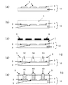
絶縁基板上に配線および電極パッドが形成された配線基板に、外部接続用電極として、突起形状を有するバンプを形成したバンプ付き配線基板は、COF方式の実装パッケージ用基板や、半導体検査用のフィルムプローブとして利用されている。このバンプ付き配線基板の一例を図6に示す。図6において、図6(a)はバンプ付き配線基板11を上面から見た図であり、図6(b)は、図6(a)のA−A断面図であり、絶縁基板1の上に配線2および電極パッド3が形成されており、この電極パッド3上にバンプ4が形成されている。
A wiring board with bumps in which bumps having protrusions are formed as external connection electrodes on a wiring board in which wirings and electrode pads are formed on an insulating substrate are used for COF mounting package substrates and semiconductor inspection films. It is used as a probe. An example of this bumped wiring board is shown in FIG. 6A is a view of the
ここで用いられるバンプ4の形成方法として、図7(a)に示すように、配線基板10の上をレジスト膜5で覆いつつも電極パッド3上にレジスト膜5のない開口部50を有するレジストパターン形成基板12を得た後、図7(b)のようにレジスト膜5の開口部50を埋めるように、金属を含有する導電性ペーストを充填したり、金属めっきを行った後に、図7(c)のようにレジスト膜5を除去して所定高さのバンプ5を得る方法が知られている。
As a method of forming the
ところが、図8(a)〜図8(c)に示すように、導電性ペーストの充填においては、開口部毎の充填量のバラツキ、金属めっきにおいてはめっき液内における電流密度のバラツキにより、最終的なバンプ高さにバラツキが生じる。 However, as shown in FIGS. 8A to 8C, when filling the conductive paste, the final filling amount varies depending on the filling amount for each opening, and in metal plating, the current density varies in the plating solution. The bump height varies.
特に、電子機器の高集積化が進む昨今においてバンプ高さのバラツキ、すなわち電極高さのバラツキは、COF方式の実装および、半導体検査用のフィルムプローブ用途のいずれにおいても接触不良トラブルの原因となる。 In particular, as electronic devices become more highly integrated, bump height variations, that is, electrode height variations, cause contact failure troubles in both COF mounting and film probe applications for semiconductor inspection. .
一方、電極として突起形状を有するバンプを用いず、配線2を電極に用いる用途があるが、このような場合においても配線厚みが一定せず、すなわち電極高さが一定せず、接触不良トラブルの原因となることがある。
On the other hand, there is a use in which the
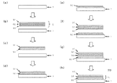
そこで、電極高さを揃える方法として種々のものが提案されており、中でも特許文献1ではバンプ高さの均一化に関し、図9(a)〜図9(d)で図示するように所望のバンプ高さ(H0)以上の厚みのレジスト膜5を形成し、レジスト膜5の開口部50に、所望のバンプ高さ以上のバンプ用金属を着設し、次いでバンプ用金属をレジスト膜5とともに高さがH0になるように所定量削り、その後、残ったレジスト膜5を取り除くことで所定高さのバンプを形成する方法が記されている。
Therefore, various methods for aligning the electrode height have been proposed, and in particular,
ところが、特許文献1で対象としている基板は平坦でかつ変形しにくい半導体材料からなるものであり、特許文献1の内容そのままを、COFやフィルムプローブに使用するフレキシブルな材料を絶縁基板とする配線基板に適用すると、配線2が形成されていない面の吸着ステージへの固定に際して、吸着穴による凹みが部分的に生じ、レジスト膜の開口部にバンプ用金属を充填したレジストパターン形成基板12の表面が湾曲や傾斜した状態で固定される(図10(a))。この状態で、バンプ用金属をレジスト膜5とともに削った場合、研磨面と絶縁基板表面との距離が一定しないため(図10(b))、結果としてバンプ高さにバラツキが生じてしまう。
However, the substrate targeted in
本発明は上記のような背景を考慮してなされたものであり、フレキシブルな材料を基板とする配線基板の電極高さを均一化方法およびこれを用いた配線基板の製造方法を提供しようとするものである。
The present invention has been made in view of the above-described background, and intends to provide a method for uniformizing the electrode height of a wiring board using a flexible material as a board and a method for manufacturing a wiring board using the same. Is.
上記の課題を解決するための請求項1に記載の発明は、絶縁基板及び絶縁基板の表面にパターン形成された配線を最小構成単位とする配線基板において、他の部品と接続または接触する電極部分の表面高さを均一化する配線基板の電極高さ均一化方法であって、
配線基板の配線が形成されていない側の面を平坦な補強板に貼り合わせた状態で、配線基板の配線が形成されている側の面に、研磨板の研磨作用面を対向配置して面方向に相対運動をさせることで摩擦力を生じさせて、前記電極部分の表面高さが均一になるように表面研磨を行った後、配線基板を前記補強板から外す配線基板の電極高さ均一化方法で、
前記配線基板の配線が形成されていない側の面を平坦な補強板と貼り合わせるのに際して、接着性を有する樹脂からなる接着層で、前記接着層に対して離型性を有する表面を備えた離型層を挟み込んだ、3層構造の積層体を用いることを特徴としている。
The invention according to
In a state where the surface of the wiring board on which the wiring is not formed is bonded to a flat reinforcing plate, the surface of the wiring board on which the wiring is formed is opposed to the surface on which the polishing plate is disposed. by causing frictional forces by causing relative movement in a direction, after the surface height of the electrode portion is subjected to surface polishing to be uniform, the electrode height of the wiring substrate to the external wiring substrate from the reinforcing plate In a uniform way ,
When the surface of the wiring board on which the wiring is not formed is bonded to a flat reinforcing plate, the adhesive layer is made of an adhesive resin, and has a surface having releasability with respect to the adhesive layer. A laminate having a three-layer structure sandwiching a release layer is used .
この発明によれば、配線基板は平坦な補強板で固定されるので、フレキシブルな絶縁基板を用いた配線基板であっても平坦な状態にして表面研磨が行えるので、研磨後の電極高さを均一にすることが出来る。また、この発明によれば、表面研磨時には、配線基板を補強板に固定支持しつつも、表面研磨終了後は両者を容易に引き離すことが出来る。 According to the present invention, since the wiring board is fixed with a flat reinforcing plate, even a wiring board using a flexible insulating substrate can be subjected to surface polishing in a flat state. It can be made uniform. In addition, according to the present invention, at the time of surface polishing, the wiring board can be fixedly supported on the reinforcing plate, but both can be easily separated after the surface polishing is completed.
請求項2に記載の発明は、請求項1に記載の配線基板の電極高さ均一化方法であって、配線基板上の電極が、配線が形成されている面に開口部を有するレジスト膜を形成した後に前記開口部に金属を充填してからレジスト膜を除去して得られる突起形状を有するバンプであって、レジスト膜の開口部にバンプ用金属が充填された状態で、配線基板の配線が形成されていない側の面を平坦な補強板に貼り合わせた状態で、前記バンプ用金属を前記レジスト膜とともに表面研磨した後、前記補強板から外すとともに、レジスト膜を除去することを特徴としている。
The invention according to
この発明によれば、突起電極であるバンプの高さを均一化することが出来、レジスト膜がある状態で表面研磨を行うことから、表面研磨時にバンプに加わる応力を緩和することが出来る。 According to the present invention, the height of the bumps that are the protruding electrodes can be made uniform, and the surface polishing is performed in a state where the resist film is present, so that the stress applied to the bumps during the surface polishing can be relieved.
請求項3に記載の発明は、請求項1または請求項2に記載の配線基板の電極高さ均一化方法であって、前記絶縁基板がフレキシブル性を有するものである。
The invention according to
請求項4に記載の発明は、請求項1〜3のいずれかに記載の配線基板の電極高さ均一化方法であって、前記配線基板の配線が形成されていない側の面と平坦な補強板を貼り合わせる前記積層体の、周辺部の離型層を除去して接着層同士を密着させたことを特徴としている。
The invention according to
請求項5に記載の発明は、請求項1〜4いずれかに記載の配線基板の電極高さ均一化方法であって、前記補強板の厚みが0.5mm以上であることを特徴としている。 A fifth aspect of the present invention is the wiring board electrode height equalizing method according to any one of the first to fourth aspects, wherein the thickness of the reinforcing plate is 0.5 mm or more.
請求項6に記載の発明は、請求項1〜5のいずれかに記載の配線基板の電極高さ均一化方法であって、前記補強板が金属板であることを特徴としている。 A sixth aspect of the invention is the wiring board electrode height equalizing method according to any one of the first to fifth aspects, wherein the reinforcing plate is a metal plate.
請求項7に記載の発明は、請求項1〜6のいずれかに記載の配線基板の電極高さ均一化方法であって、前記補強板の、前記配線基板の配線が形成されていない側の面と貼り合わせる面を、貼り合わせを行う前に研磨して平滑化することを特徴としている。
The invention according to
請求項8に記載の発明は、請求項1〜7のいずれかに記載の配線基板の電極高さ均一化方法であって、前記電極の用途がコンタクトプローブ用電極であることを特徴としている。
The invention described in claim 8 is the method for equalizing the electrode height of the wiring board according to any one of
請求項9に記載の発明は、絶縁基板及び絶縁基板の表面にパターン形成された配線を最小構成単位とする配線基板の製造方法であって、他の部品と接続または接触する電極部分の表面高さを、請求項1〜8のいずれかに記載の配線基板の電極高さ均一化方法により、均一化することを特徴としている。
The invention according to
フレキシブルな絶縁基板上の電極高さが均一化され、他の部品との接続等の用途において接触不良を低減できる。また、電極高さの均一化の工程で配線基板自体に機械的なストレスを強いることもない。 The height of the electrode on the flexible insulating substrate is made uniform, and contact failure can be reduced in applications such as connection with other components. Further, no mechanical stress is imposed on the wiring board itself in the step of equalizing the electrode height.
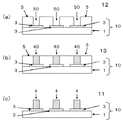
以下、本発明の実施の形態について、図面を参照して説明する。まず、図1は、配線基板10の状態から、レジストパターン形成基板12のレジスト膜5の開口部50にバンプ用金属を充填するまでの工程を表したものである。
Embodiments of the present invention will be described below with reference to the drawings. First, FIG. 1 shows a process from the state of the
図1(a)は絶縁基板1の上に、図示しない配線2と電極パッド3が形成された配線基板10の断面図である。
FIG. 1A is a cross-sectional view of a
絶縁基板1の材質としては、繊維強化ポリエステル樹脂、ポリイミド樹脂または液晶ポリエステル樹脂が好適に用いられるが、それに限定されず用途に応じ、耐熱性、フレキシブル性等の特性を活かした絶縁材料が選ばれる。
As the material of the insulating
配線2および電極パッド3の材質は、導電性と耐食性を兼ね備えた金属および金属合金
が用いられ、一般的に、ニッケル、ニッケル合金、銅、銅合金が用いられるが、それに限定されず他の導電材料であってもよく、耐食性を高めるために、金、スズ等を、その表面に積層してもよい。また、配線2および電極パッド3のパターンは、絶縁基板1上の一面を覆うように積層された前記導電材料を、パターンエッチングすることにより形成している。
As the material of the
図1(b)は配線基板10の、配線2および電極パッド3が形成された側の全面にレジスト膜5を形成した状態である。レジスト膜5は、感光性レジストの塗布または感光性ドライフィルムの貼り合わせにより、配線基板10上に積層される。レジスト膜5の膜厚は所望するバンプ高さより2〜15μm分厚くする。所望するバンプ高さに対する厚みの超過分が小さいと、後にレジスト膜5の開口部50にバンプ金属40を充填する際の高さバラツキの影響で一部の開口部50上に多量のバンプ金属40が溢れることになり、超過分が大きいとレジスト材料の使用量が増し、研磨にも時間を要するので好ましくない。
FIG. 1B shows a state in which a resist
図1(c)は、フォトリソグラフィー法で、レジスト膜5に開口部50を形成するために、レジスト膜上に露光マスク6を配置している状態を示す。この後、露光・現像によりレジスト膜5が取り除かれた部分が開口部50となる。なお、本実施の形態でレジスト膜5はポジ型の感光性のものになっているが、ネガ型であっても何ら問題なく、図1(d)のように、所望の開口部50が得られれば良く、この後、開口部50にバンプ金属40を充填する。
FIG. 1C shows a state in which the
バンプ金属40の充填としては、バンプ用金属を主成分とする導電性ペーストを印刷法を用いて充填し乾燥・硬化させる方法やめっき処理によりバンプ金属40を析出する方法を用いる。バンプ用金属としては、一般的に、ニッケル、ニッケル合金、銅、銅合金が用いられる。バンプ金属40の充填量としては、レジスト膜5の上面をわずかに突出する状態を目安とするが、図1(e)のようにバラツキが生じる。
As the filling of the
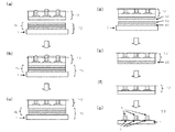
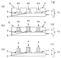
以上が、レジストパターン形成基板12のレジスト膜5の開口部50にバンプ金属40を充填したバンプ金属充填基板13を得るまでの工程であるが、次に、このバンプ金属充填基板13を固定して配線2の形成された面を研磨する際に、配線2が形成されていない面と貼り合わせるための基板固定用補強板について図2を用いて説明する。
The above is the process until the bump metal-filled
図2(a)は、バンプ金属充填基板13を平坦な状態に固定するための基礎となる補強板7である。補強板7としては、凹凸のない平坦な表面が得られれば、金属、ガラス、セラミックス、プラスチック等、素材を問わないが、取扱い易さや再使用のし易さから金属が好適であり、中でもコストを考慮すれば鉄やステンレスが優れる。また、湾曲や変形のし難さから厚みは0.5mm以上あることが望ましい。また、補強板7の表面を研磨することで、平坦度を改善しておくことも好ましく、特に、再使用する場合に有効である。
FIG. 2A shows a reinforcing
図2(b)〜図2(h)は補強板7とバンプ金属充填基板13を貼り合わせるための積層体ALを補強板7の表面上に形成する工程を表したものである。ここで、積層体ALは補強板7よりも小さく、バンプ金属充填基板13と同等以上の大きさで、バンプ金属充填基板13の全面を平坦に固定するためのものである。
FIG. 2B to FIG. 2H show a process of forming a laminated body AL for bonding the reinforcing
図2(b)〜図2(e)は補強板7に積層体ALを構成する接着層82を貼り付ける工程であるが、接着層82の両面を離型層81および離型層83で挟んだ積層フィルム8を用意する。ここで、積層フィルム8の離型層81および離型層83は、接着層82に対する離型性を有する離型剤を表面に塗布した、厚みが10〜50μmの高分子フィルムまたは紙である。この厚みが薄過ぎても厚過ぎても取扱い難くなり作業性が低下する。また、接着層82は補強板7に対して接着性を有する樹脂からなり、厚みが20〜50μmであれば取扱に好適である。なお、この積層フィルム8として、以上の3層構成からなるドライフィルム型レジストのような市販品を利用することが可能であり、ドライフィルム型レジストを用いた場合、レジスト層が接着層82に該当し、保護フィルムおよびベースフィルムが離型層81または離型層83の何れかに相当する。
FIG. 2B to FIG. 2E are steps for attaching the
図2(b)において、積層フィルム8は、補強板7に対向する離型層83を剥離(図2(c))した後に、補強板7の上部に位置合わせされ、補強板7に貼り付けられ(図2(d))、次に離型層81も剥離され、補強板7上に接着層82のみが貼られた状態となる。
In FIG. 2 (b), the laminated film 8 is aligned with the upper portion of the reinforcing
次に、積層フィルム9が用意される。積層フィルム9は、積層フィルム8と同じ構成であり、離型層91および離型層93は、接着層92に対して離型性を有する離型剤を表面に塗布した、厚みが10〜50μmの高分子フィルムまたは紙であり、接着層92は厚みが20〜50μmの絶縁基板1に対して接着性を有する樹脂からなる。また、積層フィルム8と同様、積層フィルム9として、ドライフィルム型レジストのような市販品を使用することが可能である。なお、積層フィルム8と積層フィルム9は同じ形状、大きさである。
Next, the
積層フィルム9は、補強板7の上部に貼られた接着層82と位置合わせを行い(図2(f))、接着層82の上に積層し(図2(g))、次に両面接着フィルム9の離型層91を剥離する。
The
以上の工程により、補強板7の面上に接着層82と離型層93と接着層92の3層からなる積層体ALが形成された基板固定用補強板70が出来上がる(図2(h))。
Through the above-described steps, the substrate
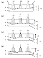
そこで、この基板固定用補強板70にバンプ金属充填基板13を固定して、表面研磨する工程を次に説明する。
Therefore, a process of fixing the bump metal-filled
まず、図3(a)のように、基板固定用補強板70の積層体ALに対してバンプ金属充填基板13の位置合わせを行ってから、バンプ金属充填基板13を基板固定用補強板70に貼り合わせる。こうすることで、バンプ金属充填基板13の配線2が形成されていない側の面が積層体ALの接着層92を介して基板固定用補強板70に固定される(図3(b))。
First, as shown in FIG. 3A, the bump metal-filled
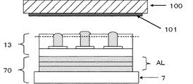
次に、バンプ金属充填基板13のレジスト膜5の高さが所望のバンプ高さになるまでバンプ金属充填基板13の配線2が形成されている側の表面研磨を行う。
Next, surface polishing of the bump metal-filled
表面研磨では、図4に示すような研磨板100を用いてバンプ金属40およびレジスト膜5の研磨を行う。研磨板100は所定の平坦度および補強板7と平行に配置され、一定の加重で研磨作業が行える。特に高精度な研磨を行う場合には、半導体ウェハなどの研磨に用いられるラッピング装置やポリッシング装置を用いることも可能である。配線2が形成されている側の面をラッピング装置またはポリッシング装置の研磨作用面(研磨板100の表面に相当)とを対向配置し、バンプ金属40とレジスト膜5の双方を研磨可能な研磨剤101をその間に塗布し、基板固定用補強板70のバンプ金属充填基板13のない側の面から加重をかけるとともに、面方向に沿って、基板固定用補強板70と研磨作用面で相対運動させることで摩擦力を生じさせて研磨が出来る。
In the surface polishing, the
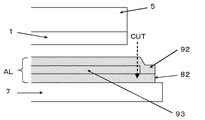
なお、面方向に沿った摩擦力が生じる際も、積層体ALの離型層93と接着層82および離型層93と接着層92の間で面方向にスベリが生じることはない。ただし、積層体ALの周辺部で接着力が低下して剥がれが生じることがある。そこで、図5に示すように積層体ALの周辺部の離型層93を除去して接着層82と接着層92を密着させておけば、表面研磨時も、積層体ALの周辺部で剥がれを生じることはなくなる。積層体ALの周辺部の離型層93の除去は、図2(f)に示す、積層フィルム9を接着層82に積層する前の段階で行っておくのが良い。
Even when a frictional force is generated along the surface direction, no slip occurs in the surface direction between the
図3(c)のようにレジスト膜5が所定の高さになるまで、バンプ金属40およびレジスト膜5を研磨すると、バンプ金属充填基板13と基板固定用補強板70に固定する必要がなくなる。そこで、バンプ金属充填基板13を基板固定用補強板70から離そうとすれば、接着層92と離型層93の界面または接着層82と離型層93の界面で簡単に剥離し、仮に接着層82と離型層93の界面で剥離した場合でも、接着層92から離型層93を簡単に剥がすことが出来、バンプ金属充填基板13の配線2が形成されていない面には接着層93のみが残る。ここで、図5のように、積層体ALの周辺部の離型層を除去しておいた場合においては、研磨後に図5のCUTと示している位置に切れ込みを入れておく必要がある。
When the
次に、バンプ金属充填基板13の、配線2が形成されていない側の面に残った接着層92を薬液で溶かして除去し(図3(f))、更にレジスト膜5を薬液で溶かして除去すれば、所望高さのバンプ4が形成されたバンプ付き配線基板11が得られる。なお、図3(f)において、接着層92を除去しているが、接着層92の材料を選べばレジスト膜5を同時に除去することも可能である。また、接着粗92に先だってレジスト膜5を除去しても良い。
Next, the
なお、バンプ4を形成しない場合の電極高さ均一化は、図1(a)の状態の配線基板10を図2(h)の基板固定用補強板70に貼り付けた状態で、配線2が形成されている側の面を研磨し、その後は図3(d)〜図3(e)と同じ処理を行えば良い。当然のことながら、配線基板全面の配線高さも均一化される。
When the
以上のように、積層体ALが離型層93を接着層82および接着層92で挟み込んだ3層構造であるため、研磨後にバンプ金属充填基板13(または配線基板10)を補強板7から離すことが容易であり、その後に残った接着層の除去も薬液により、容易に行えることが出来る。これが、3層構造ではなく接着層のみ1層であったら、引き剥がそうとすると、補強板7は平坦さを保つための厚さであるため、バンプ金属充填基板13に、引っ張りや屈曲による応力が加わり、寸法変化等の弊害が加わる。また、接着層を薬液で溶かそうとすると、接着面全面に薬液を接することが出来ないため、長時間薬液に浸透させる必要が生じて好ましくない。
As described above, since the laminate AL has a three-layer structure in which the
本発明は、配線基板における外部接続用電極の高さ均一化に係り、特に他部品等との電気的接続の信頼性が要求される配線基板の製造に好適なものである。 The present invention relates to uniform height of external connection electrodes on a wiring board, and is particularly suitable for manufacturing a wiring board that requires reliability of electrical connection with other components.
1 絶縁基板
2 配線
3 電極パッド
4 バンプ
5 レジスト膜
6 露光マスク
7 補強板
8 積層フィルム
9 積層フィルム
10 配線基板
11 バンプ付き配線基板
12 レジストパターン形成基板
13 バンプ金属充填基板
70 基板固定用補強板
81 離型層
82 接着層
83 離型層
91 離型層
92 接着層
93 離型層
AL 積層体
H0 所望するバンプ高さ
DESCRIPTION OF
Claims (9)
配線基板の配線が形成されていない側の面を平坦な補強板に貼り合わせた状態で、配線基板の配線が形成されている側の面に、研磨板の研磨作用面を対向配置して面方向に相対運動をさせることで摩擦力を生じさせて、前記電極部分の表面高さが均一になるように表面研磨を行った後、配線基板を前記補強板から外す配線基板の電極高さ均一化方法で、
前記配線基板の配線が形成されていない側の面を平坦な補強板と貼り合わせるのに際して、接着性を有する樹脂からなる接着層で、前記接着層に対して離型性を有する表面を備えた離型層を挟み込んだ、3層構造の積層体を用いることを特徴とする配線基板の電極高さ均一化方法。 Method for uniformizing electrode height of wiring board for uniformizing surface height of electrode portion connected to or contacting other components in wiring board having minimum constituent unit of wiring formed on surface of insulating substrate and insulating substrate Because
In a state where the surface of the wiring board on which the wiring is not formed is bonded to a flat reinforcing plate, the surface of the wiring board on which the wiring is formed is opposed to the surface on which the polishing plate is disposed. by causing frictional forces by causing relative movement in a direction, after the surface height of the electrode portion is subjected to surface polishing to be uniform, the electrode height of the wiring substrate to the external wiring substrate from the reinforcing plate In a uniform way ,
When the surface of the wiring board on which the wiring is not formed is bonded to a flat reinforcing plate, the adhesive layer is made of an adhesive resin, and has a surface having releasability with respect to the adhesive layer. A method for equalizing the electrode height of a wiring board, comprising using a laminate having a three-layer structure with a release layer interposed therebetween .
レジスト膜の開口部にバンプ用金属が充填された状態で、配線基板の配線が形成されていない側の面を平坦な補強板に貼り合わせた状態で、前記バンプ用金属を前記レジスト膜とともに表面研磨した後、前記補強板から外すとともに、レジスト膜を除去することを特徴とする配線基板の電極高さ均一化方法。 2. The method for equalizing electrode height of a wiring board according to claim 1, wherein an electrode on the wiring board is formed by forming a resist film having an opening on a surface on which the wiring is formed, and then applying a metal to the opening. When it is a bump having a protrusion shape obtained by removing the resist film after filling,
With the bump metal filled in the opening of the resist film, the surface of the wiring board on which the wiring is not formed is bonded to a flat reinforcing plate, and the bump metal is surfaced together with the resist film. A method of uniformizing the electrode height of a wiring board, comprising removing the resist film and removing the resist film after polishing.
Priority Applications (1)
| Application Number | Priority Date | Filing Date | Title |
|---|---|---|---|
| JP2013038487A JP6132425B2 (en) | 2013-02-28 | 2013-02-28 | Method for equalizing electrode height of wiring board and method for manufacturing wiring board using the same |
Applications Claiming Priority (1)
| Application Number | Priority Date | Filing Date | Title |
|---|---|---|---|
| JP2013038487A JP6132425B2 (en) | 2013-02-28 | 2013-02-28 | Method for equalizing electrode height of wiring board and method for manufacturing wiring board using the same |
Publications (2)
| Publication Number | Publication Date |
|---|---|
| JP2014166653A JP2014166653A (en) | 2014-09-11 |
| JP6132425B2 true JP6132425B2 (en) | 2017-05-24 |
Family
ID=51616652
Family Applications (1)
| Application Number | Title | Priority Date | Filing Date |
|---|---|---|---|
| JP2013038487A Expired - Fee Related JP6132425B2 (en) | 2013-02-28 | 2013-02-28 | Method for equalizing electrode height of wiring board and method for manufacturing wiring board using the same |
Country Status (1)
| Country | Link |
|---|---|
| JP (1) | JP6132425B2 (en) |
Families Citing this family (2)
| Publication number | Priority date | Publication date | Assignee | Title |
|---|---|---|---|---|
| CN105142332B (en) * | 2015-09-18 | 2018-03-13 | 刘炜 | A kind of FPC and its processing technology with conductive reinforced structure |
| JP6691816B2 (en) * | 2016-05-18 | 2020-05-13 | 東京応化工業株式会社 | Method for manufacturing sealed body |
Family Cites Families (6)
| Publication number | Priority date | Publication date | Assignee | Title |
|---|---|---|---|---|
| JPH07297196A (en) * | 1994-04-25 | 1995-11-10 | Sony Corp | Method of forming bump electrode |
| JP2002100651A (en) * | 2000-09-21 | 2002-04-05 | Toppan Printing Co Ltd | Semiconductor device and manufacturing method thereof |
| JP3875886B2 (en) * | 2001-12-26 | 2007-01-31 | ソニーケミカル&インフォメーションデバイス株式会社 | Manufacturing method of flexible wiring board |
| JP2007243097A (en) * | 2006-03-13 | 2007-09-20 | Matsushita Electric Ind Co Ltd | Method of forming conductive pattern |
| JP5152601B2 (en) * | 2010-06-01 | 2013-02-27 | 日立化成工業株式会社 | Method for manufacturing connection board using thin plate-like article and method for manufacturing multilayer wiring board |
| JP5650945B2 (en) * | 2010-07-27 | 2015-01-07 | 三菱製紙株式会社 | Photosensitive film for sandblasting |
-
2013
- 2013-02-28 JP JP2013038487A patent/JP6132425B2/en not_active Expired - Fee Related
Also Published As
| Publication number | Publication date |
|---|---|
| JP2014166653A (en) | 2014-09-11 |
Similar Documents
| Publication | Publication Date | Title |
|---|---|---|
| TWI250636B (en) | A semiconductor device and its fabrication method | |
| JP4543089B2 (en) | Semiconductor device | |
| KR101084924B1 (en) | Semiconductor device and manufacturing method thereof | |
| JP5147677B2 (en) | Manufacturing method of resin-sealed package | |
| JP4835124B2 (en) | Semiconductor IC-embedded substrate and manufacturing method thereof | |
| JP6041731B2 (en) | Interposer and electronic component package | |
| JP5998792B2 (en) | Semiconductor IC-embedded substrate and manufacturing method thereof | |
| JP2013214713A (en) | Metal foil with carrier | |
| CN101282637A (en) | Flexible Circuit Board Surface Mount Carrier | |
| TW201626864A (en) | Cover film with high dimensional stability and manufacturing method of flexible printed circuit board | |
| JP6132425B2 (en) | Method for equalizing electrode height of wiring board and method for manufacturing wiring board using the same | |
| TWI590726B (en) | Electronic package, package carrier and manufacturing method of the same | |
| TWI362908B (en) | ||
| JP2009182202A (en) | Manufacturing method of semiconductor device | |
| JP5258838B2 (en) | Semiconductor device | |
| JP5456113B2 (en) | Resin sealed package | |
| CN115915595A (en) | Buried resistance circuit board and processing method | |
| JP5477372B2 (en) | Functional element-embedded substrate, manufacturing method thereof, and electronic apparatus | |
| JP2009081367A (en) | Semiconductor device and manufacturing method thereof | |
| JP3444787B2 (en) | Film carrier tape for mounting electronic components and method of manufacturing film carrier tape for mounting electronic components | |
| KR101044133B1 (en) | Carrier for manufacturing printed circuit board, manufacturing method thereof and manufacturing method of printed circuit board using same | |
| JP4158659B2 (en) | Manufacturing method of electronic component mounting circuit board | |
| JP5288898B2 (en) | Adhesive sheet sticking device and sticking method, and electronic component mounting device and mounting method | |
| KR101897609B1 (en) | Method for filling resin on circuit board | |
| JP4345464B2 (en) | Method for manufacturing circuit board member to which electronic component is bonded |
Legal Events
| Date | Code | Title | Description |
|---|---|---|---|
| A621 | Written request for application examination |
Free format text: JAPANESE INTERMEDIATE CODE: A621 Effective date: 20151225 |
|
| A977 | Report on retrieval |
Free format text: JAPANESE INTERMEDIATE CODE: A971007 Effective date: 20161026 |
|
| A131 | Notification of reasons for refusal |
Free format text: JAPANESE INTERMEDIATE CODE: A131 Effective date: 20161129 |
|
| A521 | Written amendment |
Free format text: JAPANESE INTERMEDIATE CODE: A523 Effective date: 20170120 |
|
| TRDD | Decision of grant or rejection written | ||
| A01 | Written decision to grant a patent or to grant a registration (utility model) |
Free format text: JAPANESE INTERMEDIATE CODE: A01 Effective date: 20170412 |
|
| A621 | Written request for application examination |
Free format text: JAPANESE INTERMEDIATE CODE: A621 Effective date: 20170417 |
|
| A61 | First payment of annual fees (during grant procedure) |
Free format text: JAPANESE INTERMEDIATE CODE: A61 Effective date: 20170417 |
|
| R150 | Certificate of patent or registration of utility model |
Ref document number: 6132425 Country of ref document: JP Free format text: JAPANESE INTERMEDIATE CODE: R150 |
|
| R250 | Receipt of annual fees |
Free format text: JAPANESE INTERMEDIATE CODE: R250 |
|
| LAPS | Cancellation because of no payment of annual fees |