JP6126600B2 - Circuit apparatus and method for transmitting signals - Google Patents
Circuit apparatus and method for transmitting signals Download PDFInfo
- Publication number
- JP6126600B2 JP6126600B2 JP2014525315A JP2014525315A JP6126600B2 JP 6126600 B2 JP6126600 B2 JP 6126600B2 JP 2014525315 A JP2014525315 A JP 2014525315A JP 2014525315 A JP2014525315 A JP 2014525315A JP 6126600 B2 JP6126600 B2 JP 6126600B2
- Authority
- JP
- Japan
- Prior art keywords
- data
- signal
- clock
- differential
- downstream
- Prior art date
- Legal status (The legal status is an assumption and is not a legal conclusion. Google has not performed a legal analysis and makes no representation as to the accuracy of the status listed.)
- Expired - Fee Related
Links
Images


Classifications
-
- H—ELECTRICITY
- H04—ELECTRIC COMMUNICATION TECHNIQUE
- H04L—TRANSMISSION OF DIGITAL INFORMATION, e.g. TELEGRAPHIC COMMUNICATION
- H04L7/00—Arrangements for synchronising receiver with transmitter
- H04L7/0008—Synchronisation information channels, e.g. clock distribution lines
-
- H—ELECTRICITY
- H04—ELECTRIC COMMUNICATION TECHNIQUE
- H04L—TRANSMISSION OF DIGITAL INFORMATION, e.g. TELEGRAPHIC COMMUNICATION
- H04L7/00—Arrangements for synchronising receiver with transmitter
- H04L7/04—Speed or phase control by synchronisation signals
- H04L7/10—Arrangements for initial synchronisation
-
- G—PHYSICS
- G06—COMPUTING; CALCULATING OR COUNTING
- G06F—ELECTRIC DIGITAL DATA PROCESSING
- G06F13/00—Interconnection of, or transfer of information or other signals between, memories, input/output devices or central processing units
- G06F13/38—Information transfer, e.g. on bus
- G06F13/40—Bus structure
-
- H—ELECTRICITY
- H04—ELECTRIC COMMUNICATION TECHNIQUE
- H04B—TRANSMISSION
- H04B1/00—Details of transmission systems, not covered by a single one of groups H04B3/00 - H04B13/00; Details of transmission systems not characterised by the medium used for transmission
- H04B1/02—Transmitters
- H04B1/04—Circuits
Description
本発明は、請求項1のプリアンブルに記載の回路装置、ならびに請求項15のプリアンブルに記載の対応する方法に関する。
The invention relates to a circuit arrangement according to the preamble of
ビット伝送層または物理層(physical layer:PHY)は、OSI(Open Systems Interconnection)参照モデルとも呼ばれるOSI階層モデルの最下位層であり、コンピュータネットワークにおける通信プロトコルの設計基準としても役に立つ、国際標準化機構(International Standards Organisation:ISO)の階層モデルを示す。 The bit transmission layer (physical layer: PHY) is the lowest layer of the OSI hierarchical model, also called the OSI (Open Systems Interconnection) reference model, and is also an international standardization mechanism (useful as a design standard for communication protocols in computer networks). The hierarchical model of International Standards Organization (ISO) is shown.
物理層(PHY)は、結合、順方向誤り訂正(Forward Error Correction:FEC)、電力制御、拡散(符号分割多元接続)(Code Division Multiple Access:CDMA)等に関与し、およびデータもアプリケーションも識別せず、0と1のみを識別する。PHYは、その上のセキュリティ層(データリンク層)(Data Link Layer:DLL)が、特に、媒体アクセス制御(Media Access Control:MAC)層と呼ばれる部分層を利用可能な論理チャネル(UMTS(Universal Mobile Telecommunications System)用のトランスポートチャネル)を形成する。 The physical layer (PHY) is involved in combining, forward error correction (FEC), power control, spreading (Code Division Multiple Access (CDMA)), etc., and also identifies data and applications Only 0 and 1 are identified. The PHY is a logical channel (UMTS (Universal Mobile) that can use a partial layer called a media access control (MAC) layer, in particular, a security layer (data link layer) (DLL) above the PHY. A transport channel for Telecommunications System).
原理的に、D−PHYは、モバイル装置内のコンポーネント間の通信リンクのためのフレキシブルで、低コストで、高速のシリアルインタフェースを実現できる。 In principle, D-PHY can implement a flexible, low cost, high speed serial interface for communication links between components in mobile devices.
図4Aに示すように、最新の携帯電話において、データソース、例えば、アプリケーションプロセッサは、関連するデータシンク上、例えば、関連するディスプレイ上での表示のために、イメージデータをD−PHY信号として、MIPI−DSI(Mobile Industry Processor Interface−Display Serial Interface)に供給する。また、アプリケーションプロセッサ等のデータシンクは、関連するデータソースから、例えば、関連するカメラから、MIPI−CSI(Camera Serial Interface)を介して、D−PHYフォーマットでイメージデータを受信することができる。 As shown in FIG. 4A, in a modern mobile phone, a data source, eg, an application processor, uses image data as a D-PHY signal for display on an associated data sink, eg, an associated display. Supplied to MIPI-DSI (Mobile Industry Processor Interface-Display Serial Interface). In addition, a data sink such as an application processor can receive image data in a D-PHY format from an associated data source, for example, an associated camera via MIPI-CSI (Camera Serial Interface).
D−PHYプロトコルに基づくDSIまたはDSI−2またはCSIまたはCSI−2またはCSI−3は、4つ以下の差動データラインと、差動クロックラインとを備え、これらは、銅ケーブルを用いて、該アプリケーションプロセッサを該ディスプレイおよび/または該カメラに接続する。差動データライン当たりのデータ転送速度は、最高で1.5Gbps(ギガビット/秒)である。 DSI or DSI-2 or CSI or CSI-2 or CSI-3 based on the D-PHY protocol comprises no more than 4 differential data lines and differential clock lines, which use copper cables, The application processor is connected to the display and / or the camera. The maximum data transfer rate per differential data line is 1.5 Gbps (gigabit / second).
1〜4つの差動データ信号および差動クロックラインを介した、この従来のD−PHY−DSI信号またはD−PHY−CSI信号の送信および受信は、マスター側のモジュール(データソース、例えば、カメラおよび/またはアプリケーションプロセッサ)と、スレーブ側のモジュール(データシンク、例えば、アプリケーションプロセッサおよび/またはディスプレイユニット)との間の(データレーンCH0+,CH0−およびCH1+,CH1−と呼ばれる)2つのデータチャネルおよび(クロックレーンCLK+,CLK−と呼ばれる)クロックラインを手段として、図4BのD−PHYインタフェース構造に例として図示されている。 The transmission and reception of this conventional D-PHY-DSI signal or D-PHY-CSI signal via one to four differential data signals and a differential clock line is performed by a module on the master side (data source, eg, camera And / or application processor) and two data channels (referred to as data lanes CH0 +, CH0− and CH1 +, CH1−) between the slave side module (data sink, eg application processor and / or display unit) and This is illustrated by way of example in the D-PHY interface structure of FIG. 4B using clock lines (referred to as clock lanes CLK +, CLK−) as a means.
この状況において、図4Aを見て分かるように、各関連するディプレイのための、または、各関連するカメラのためのデータ伝送には、最高10の銅線(例えば、2つのデータラインの4倍と、2つのクロックラインの1倍)を要する。 In this situation, as can be seen in FIG. 4A, for data transmission for each associated display or for each associated camera, up to 10 copper wires (eg, 4 of 2 data lines). Twice as much as two clock lines).
ラインの数の望ましい低減を考えると、シリアル化された信号伝送を考慮すべきである。しかし、そのようなシリアル化は、エラーを起こしやすく、不安定なことが多い。 Given the desirable reduction in the number of lines, serialized signal transmission should be considered. However, such serialization is error-prone and often unstable.
上述した欠点および不十分な点を発端として、ならびに概略が説明された従来技術を考慮して、本発明の目的は、効率的なシリアル化信号伝送を、エラーのない安定した方法で、常に実行できるように、上述したタイプの回路装置および上述したタイプの方法をさらに発展させることである。 Starting from the disadvantages and deficiencies mentioned above, and in view of the prior art outlined, the object of the present invention is to always carry out efficient serialized signal transmission in an error-free and stable manner. In order to be able to do so, it is to further develop a circuit arrangement of the type described above and a method of the type described above.
この目的は、請求項1の特徴を有する回路装置と、請求項12の特徴を有する方法によって達成される。本発明の有利な実施形態および適切なさらなる発展は、それぞれの従属項において特徴付けられている。
This object is achieved by a circuit arrangement having the features of
したがって、回路装置および方法が提案され、それを用いて、
論理レベルに基づく信号に対応するシングルエンド高速(High Speed:HS)データと、
特に、コモンモード信号に基づく信号に対応する差動低電力(Low Power:LP)データと、
がシリアル化されて、共通信号ストリームを形成する。
Therefore, a circuit device and method is proposed, using it,
Single-ended high-speed (HS) data corresponding to signals based on logic levels;
In particular, differential low power (LP) data corresponding to signals based on common mode signals;
Are serialized to form a common signal stream.
シリアル化された共通信号ストリームを伴うこの種の伝送路を用いて、HS/LPデータは、少なくとも1つのマルチプレクサを本質的に備える少なくとも1つの送信ビルディングブロック(=送信装置)によって一括化されて、シリアル化された共通データストリームとして、受信ビルディングブロック(=受信装置)へ送信される。 With this kind of transmission line with a serialized common signal stream, the HS / LP data is bundled by at least one transmission building block (= transmitter) essentially comprising at least one multiplexer, It is transmitted to the receiving building block (= receiving device) as a serialized common data stream.
少なくとも1つのデマルチプレクサを本質的に備えるこの受信装置は、該シリアルデータを細分化して、それを元の形態でHS/LPデータとして再び出力する。該送信装置に印加されたクロック(Clock:CLK)は、該マルチプレクサのクロック基準として機能し、および該共通シリアル信号ストリームに埋め込まれる。該受信装置は、このクロックを再生して、それをCLKとして再出力する。 This receiving device, which essentially comprises at least one demultiplexer, subdivides the serial data and outputs it again as HS / LP data in its original form. A clock (Clock: CLK) applied to the transmitter functions as a clock reference for the multiplexer and is embedded in the common serial signal stream. The receiver reproduces this clock and re-outputs it as CLK.
全てのデータ入力部がHSデータを処理する状況に基づく、データビルディングのための通常のアプローチは、該データが多重化されて、シリアルデータストリームとして送出されることである。 The usual approach for data building, based on the situation where all data inputs process HS data, is that the data is multiplexed and sent out as a serial data stream.
しかし、MIPI−D−PHY規格においては、いわゆるLP送信モードへのリターンは、HSデータのシグナリングに用いられる電圧レベルの範囲外の電圧振幅によって伝えられることが既に合意されている。 However, in the MIPI-D-PHY standard, it has already been agreed that the return to the so-called LP transmission mode is conveyed by a voltage amplitude outside the range of voltage levels used for HS data signaling.
これらのLP信号レベルは、既に説明したように、単純に一括化されたシリアルデータストリームのデータスペースで符号化することができない追加的な情報を示す。 These LP signal levels represent additional information that cannot be encoded in the data space of a serialized serial data stream, as already described.
本発明によれば、特に、LPデータだけを含み、HSレーンと並列に該マルチプレクサに入力される少なくとも1つの追加的な、特に仮想レーンを挿入することが提案されている。これは、このために設けられた該マルチプレクサの入力部のHSデータのための符号化スペースを拡大することなく、LP状態を伝えることを可能にする。 According to the present invention, it is proposed to insert at least one additional, in particular virtual lane, in particular containing only LP data and input to the multiplexer in parallel with the HS lane. This makes it possible to convey the LP state without expanding the coding space for HS data at the input of the multiplexer provided for this purpose.
このレーン、具体的には、テレグラムレーンと呼ぶこともできる仮想レーンは、他のシステム関連情報を運ぶのにも用いることができ、例えば、該レーンは、該シリアルデータリンクが間もなく切断されるという情報を送信するのに用いることができるであろう。 This lane, specifically a virtual lane, which can also be called a telegram lane, can also be used to carry other system related information, for example, the lane is said that the serial data link will soon be disconnected Could be used to send information.
本発明は、典型的には、シングルエンド論理レベルベースのデータ信号およびクロック信号と、特に、コモンモードベースの差動データ信号およびクロック信号の両方の、具体的には、D−PHYデータ信号またはD−PHYクロック信号、例えば、1〜4ビット幅のMIPI−D−PHYデータ信号およびMIPI−D−PHYクロック信号の、少なくとも1つのデータソース、具体的には、例えば、少なくとも高解像度カメラおよび/または画像ソースとして機能するカメラおよび/または少なくとも1つのアプリケーションプロセッサと、少なくとも1つのデータシンク、具体的には、少なくとも1つのアプリケーションプロセッサおよび/または少なくとも1つの高解像度ディスプレイユニットまたは例えば、画像シンクとして機能するディスプレイユニット、例えば、少なくとも1つのディスプレイまたは少なくとも1つのモニタとの間での、少なくとも1つのシリアルおよび/または一括の、具体的には、CSIプロトコルベースのおよび/またはCSI−2プロトコルベースのおよび/またはCSI−3プロトコルベースのおよび/またはDSIプロトコルベースのおよび/またはDSI−2プロトコルベースの送信中に適用することができる。 The present invention typically includes both single-ended logic level based data signals and clock signals, and in particular, common mode based differential data signals and clock signals, specifically D-PHY data signals or At least one data source of a D-PHY clock signal, eg, a 1-4 bit wide MIPI-D-PHY data signal and MIPI-D-PHY clock signal, specifically, for example, at least a high resolution camera and / or Or a camera and / or at least one application processor functioning as an image source and at least one data sink, in particular functioning as at least one application processor and / or at least one high-resolution display unit or eg an image sink Display units, eg, at least one serial and / or batch, in particular CSI protocol based and / or CSI-2 protocol based and at least one display or at least one monitor It can be applied during CSI-3 protocol based and / or DSI protocol based and / or DSI-2 protocol based transmission.
前述したように、本発明に関する教示を有利な方法で具体化し、さらに発展させる様々な可能性がある。このため、一方において、請求項1に従属する請求項について、および請求項12について説明し、他方においては、本発明の追加的な実施形態、特徴および効果が、以下でより詳細に、とりわけ、図1A〜図3によって図示されている例示的な実施形態によって説明されている。 As previously mentioned, there are various possibilities for implementing and further developing the teachings of the present invention in an advantageous manner. Thus, on the one hand, the claims subordinate to claim 1 and claim 12 will be described, while on the other hand, additional embodiments, features and advantages of the invention will be described in more detail below, inter alia, This is illustrated by the exemplary embodiment illustrated by FIGS.
図1A〜図4Bにおいて、類似のまたは同様の実施形態、要素または機能には、同一の参照数字が付けられている。
(発明を具体化するための最良の方法)
In FIGS. 1A-4B, similar or similar embodiments, elements or functions are labeled with the same reference numerals.
(Best method for embodying the invention)
原理的には、
本発明による送信装置Sに関する図1Aに示す実施形態によって、および
本発明による受信装置Eに関する図2Aに示す実施形態によって、
ケーブルベースのリンクを実現するおよび作動させるための、本発明による回路装置A(図1A、図2Aを参照)が得られ(本発明に関しては、互いに無関係に、送信装置Sと受信装置Eを実現すること、作動させることが可能である)、
そのリンクは、光学的に、具体的には、少なくとも1つの光学媒体に基づいて、例えば、光導波路OM(図1A、図2Aの詳細図を参照)に基づいて、例えば、少なくとも1つのガラス繊維に基づいて、および/または少なくとも1つのプラスチック繊維に基づいて多重化され、およびシリアル化され、および/または
そのリンクは、電気的にまたはガルバニックに、具体的には、少なくとも1つの電気的またはガルバニックなリンクに基づいて、例えば、少なくとも1つの銅線に基づいて、および/または例えば、少なくともプリント回路基板上に配列された少なくとも1つの電気的ラインに基づいて多重化されていない
ことが可能である。
In principle,
According to the embodiment shown in FIG. 1A for the transmitting device S according to the invention and by the embodiment shown in FIG.
A circuit arrangement A according to the invention (see FIGS. 1A and 2A) for realizing and operating a cable-based link is obtained (in the context of the invention, a transmitter S and a receiver E are realized independently of each other) Can be actuated)
The link is optically, in particular based on at least one optical medium, for example on the basis of an optical waveguide OM (see detailed views in FIGS. 1A, 2A), for example at least one glass fiber. And / or multiplexed and serialized based on at least one plastic fiber and / or the link is electrically or galvanically, in particular at least one electrical or galvanic Can be non-multiplexed, for example based on at least one copper wire, and / or, for example, based on at least one electrical line arranged on a printed circuit board, for example .
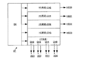
図1Aは、DSIデータ伝送インタフェースISまたはCSIデータ伝送インタフェースISへの接続のための送信装置Sの原理的構造の実施形態を示す。 FIG. 1A shows an embodiment of the principle structure of a transmitting device S for connection to a DSI data transmission interface IS or a CSI data transmission interface IS.
アプリケーションプロセッサAP内で、または、カメラKA内で生成された画像データは、D−PHY補正クロック信号CLK+,CLK−とともに、最高で4ビット幅のデータ伝送インタフェースISにおいて、4つ他のデータラインまたはデータチャネルCH0+,CH0−,CH1+,CH1−,CH2+,CH2−,CH3+,CH3−上でD−PHY信号として利用可能になっている。 The image data generated in the application processor AP or in the camera KA, together with the D-PHY correction clock signals CLK + and CLK−, is transferred to four other data lines or in the data transmission interface IS having a maximum width of 4 bits. It is made available as a D-PHY signal on the data channels CH0 +, CH0-, CH1 +, CH1-, CH2 +, CH2-, CH3 +, CH3-.
送信装置Sは、これらの信号を集積インタフェースロジックLSにおいて受け取り、そのブロックは、それらの信号が、D−PHY信号の正しい解釈のための、および高周波データストリーム(いわゆるHSデータ)と低周波データストリーム(いわゆる低速(Low Speed:LS)データ)を区別するための少なくとも1つの状態機械を有することを証明できる。 The transmitting device S receives these signals in the integrated interface logic LS and its block is used for correct interpretation of the D-PHY signals and for high frequency data streams (so-called HS data) and low frequency data streams. It can be proved that it has at least one state machine for distinguishing (so-called Low Speed (LS) data).
送信装置Sにおける次のフレーマFR(図1Bの詳細図も参照)は、入力信号の直流(Direct Current:DC)平衡を確保し、および受信側(図2Aを参照)で認識可能なフレームを生成し、そのことは、受信装置E(図2Aを参照)が、補正出力データラインまたは出力チャネルCH0+,CH0−,CH1+,CH1−,CH2+,CH2−,CH3+,CH3−に、受信したデータを再割当てすることを可能にする。 The next framer FR in the transmitting device S (see also the detailed diagram in FIG. 1B) ensures direct current (DC) balance of the input signal and generates a frame that can be recognized on the receiving side (see FIG. 2A). This means that the receiving device E (see FIG. 2A) retransmits the received data to the corrected output data line or the output channels CH0 +, CH0-, CH1 +, CH1-, CH2 +, CH2-, CH3 +, CH3-. Allows assignment.
詳細には、論理レベルベースのシングルエンドデータ信号HSD0,HSD1,HSD2,HSD3と、差動データ信号DD0+,DD0−,DD1+,DD1−,DD2+,DD2−,DD3+,DD3−の両方を、図1BによるフレーマFRに印加することができる。5b/6b符号化ブロックとして構成されたその符号器KOを用いて、図1Bによる該フレーマは、それらの差動データ信号DD0+,DD0−,DD1+,DD1−,DD2+,DD2−,DD3+,DD3−を、シングルエンド論理レベルベースのデータ信号HSD0,HSD1,HSD2,HSD3から成るストリームに埋め込む。 Specifically, both of the logic level based single-ended data signals HSD0, HSD1, HSD2, and HSD3 and the differential data signals DD0 +, DD0−, DD1 +, DD1-, DD2 +, DD2-, DD3 +, DD3- are shown in FIG. Can be applied to the framer FR. With its encoder KO configured as a 5b / 6b coding block, the framer according to FIG. 1B is able to generate the differential data signals DD0 +, DD0-, DD1 +, DD1-, DD2 +, DD2-, DD3 +, DD3- Are embedded in a stream composed of data signals HSD0, HSD1, HSD2 and HSD3 based on single-ended logic levels.
フレーマFRに隣接するマルチプレクサMU、具体的には、HS Muxは、位相ロックループとして、具体的には、CMUとして構成されたクロック発振器PSを用いて、高周波シリアルまたは一括送信信号を生成し、その信号は、出力ドライバATを用いて、送信装置Sの出力ASにおいて利用可能になっている。フレーマFRとマルチプレクサMUは、一緒にシリアライザSEを構成している。 The multiplexer MU adjacent to the framer FR, specifically, the HS Mux, generates a high-frequency serial or batch transmission signal using a clock oscillator PS configured as a phase-locked loop, specifically, CMU, The signal is made available at the output AS of the transmitting device S using the output driver AT. The framer FR and the multiplexer MU together form a serializer SE.
クロック発振器PSを用いて、クロックポートCLK+,CLK−を介して、およびインタフェースロジックLSのクロックモジュールCSを介して供給されたD−PHYクロック信号は、シリアライザSEのための、具体的には、そのマルチプレクサMUのための(クロック)基準として用いられ、および該シリアルデータストリームに、すなわち、シリアル化された出力信号に埋め込まれる。これにより、受信装置E(図2Aを参照)に伝達される共通信号ストリームSIが生成される。 The D-PHY clock signal supplied by means of the clock oscillator PS, via the clock ports CLK +, CLK− and via the clock module CS of the interface logic LS is used for the serializer SE, in particular Used as a (clock) reference for the multiplexer MU and embedded in the serial data stream, ie in the serialized output signal. Thereby, the common signal stream SI transmitted to the receiving device E (see FIG. 2A) is generated.
さらに図1Aを見て分かるように、出力ドライバATは、少なくとも1つの直接接続されたレーザLAを駆動するための、具体的には、少なくとも1つの面発光レーザ(Vertical Cavity Surface Emitting Laserdiode:VCSEL)を駆動するための一体型レーザドライバとして実装されている。 As can be further seen from FIG. 1A, the output driver AT specifically drives at least one directly connected laser LA, specifically, at least one surface emitting laser (VCSEL). It is mounted as an integrated laser driver for driving.
図2Aは、DSIデータ伝送インタフェースIEまたはCSIデータ伝送インタフェースIEへの接続のための受信装置Eの原理的構造の実施形態を示す。 FIG. 2A shows an embodiment of the principle structure of a receiving device E for connection to a DSI data transmission interface IE or a CSI data transmission interface IE.
送信装置S(図1Aを参照)によって送出されたシリアルまたは一括データは、受信装置Eの入力増幅器EVを介して受け取られ、集積クロックまたはデータリカバリCDへ供給される。 Serial or batch data sent by the transmitting device S (see FIG. 1A) is received via the input amplifier EV of the receiving device E and supplied to the integrated clock or data recovery CD.
この集積クロックまたはデータリカバリCDは、共通信号ストリームSIから元のD−PHYクロックを再生し、その後、該クロックは、インタフェースロジックLEのクロックモジュールCEを介して、再び、DSIまたはCSIが直接、利用できるようにされる。残りのシリアルデータストリームは、デマルチプレクサDMによって細分化および並列化されて、原理的には、図1BによるフレーマFRの鏡像であるデフレーマDF(図2Bも参照)へ引き渡される。デマルチプレクサDMとデフレーマDFは、一緒にデシリアライザDSを構成する。 This integrated clock or data recovery CD regenerates the original D-PHY clock from the common signal stream SI, which is then again used directly by the DSI or CSI via the clock module CE of the interface logic LE. Be made possible. The remaining serial data stream is subdivided and parallelized by the demultiplexer DM and delivered in principle to a deframer DF (see also FIG. 2B) which is a mirror image of the framer FR according to FIG. 1B. The demultiplexer DM and the deframer DF together form a deserializer DS.
詳細には、図2BのデフレーマFRは、6b/5b復号器ブロックとして構成されたその復号器DKを用いて、差動データ信号は、DD0+,DD0−,DD1+,DD1−,DD2+,DD2−,DD3+,DD3−と、シングルエンド論理レベルベースのデータ信号HSD0,HSD1,HSD2,HSD3を分けて、再並列化されたデータ信号を、それぞれの適用可能なデータラインCH0+,CH0−,CH1+,CH1−,CH2+,CH2−,CH3+,CH3−に再割り当てすることができる。 Specifically, the deframer FR of FIG. 2B uses its decoder DK configured as a 6b / 5b decoder block, and the differential data signals are DD0 +, DD0−, DD1 +, DD1-, DD2 +, DD2-, The DD3 + and DD3- and the single-end logic level-based data signals HSD0, HSD1, HSD2, and HSD3 are separated, and the re-parallelized data signals are converted into respective applicable data lines CH0 +, CH0-, CH1 +, CH1-. , CH2 +, CH2-, CH3 +, CH3-.
受信装置E内に図示されているインタフェースロジックブロックLEは、それぞれ、D−PHY論理信号の正しい解釈のための、および高周波データストリームと低周波データストリームを区別するための少なくとも1つの状態機械を備えていてもよい。 Each of the interface logic blocks LE shown in the receiving device E comprises at least one state machine for the correct interpretation of the D-PHY logic signal and for distinguishing between the high frequency data stream and the low frequency data stream. It may be.
図2Aの説明図を見ても分かるように、入力増幅器EVは、集積トランスインピーダンス増幅器として実装され、該増幅器は、フォトダイオードFDを受信装置Eに直接接続することを可能にしている。 As can be seen from the illustration of FIG. 2A, the input amplifier EV is implemented as an integrated transimpedance amplifier, which allows the photodiode FD to be directly connected to the receiver E.
このようにして、本発明によれば、回路装置S,E(図1A、図2Aを参照)に関しては、送信装置S(図1Aを参照)と受信装置E(図2Aを参照)との間で、ケーブルベースの多重化リンクを光学的に、すなわち、例えば、ガラス繊維の形態でおよび/またはプラスチック繊維の形態で構成された光導波路OMを用いて実現し、および作動させることが可能である。 Thus, according to the present invention, with respect to the circuit devices S and E (see FIGS. 1A and 2A), between the transmitting device S (see FIG. 1A) and the receiving device E (see FIG. 2A). It is thus possible to realize and operate a cable-based multiplexed link optically, i.e. with an optical waveguide OM configured, for example, in the form of glass fibers and / or in the form of plastic fibers, for example. .
全てのデータ入力部ESが、シングルエンド論理レベルベースの信号に対応するHSデータを処理する状況に基づいて、データ一括化のための通常のアプローチは、図1AによるマルチプレクサMUによって該データを多重化して、それをシリアル信号ストリームSIとして送出することである。 Based on the situation where all data inputs ES process HS data corresponding to single-ended logic level based signals, the usual approach for data bundling is to multiplex the data with the multiplexer MU according to FIG. 1A. And sending it out as a serial signal stream SI.
しかし、MIPI−D−PHY規格においては、特に、コモンモードベースの差動信号に対応するLP送信モードへのリターンは、図3に示すように、HSデータのシグナリングに用いられる電圧レベルの範囲外の電圧振幅によって伝えられることが既に合意されている。 However, in the MIPI-D-PHY standard, in particular, the return to the LP transmission mode corresponding to the common mode base differential signal is outside the range of the voltage level used for HS data signaling as shown in FIG. It has already been agreed to be conveyed by the voltage amplitude of.
これらのLP信号レベルは、既に説明したように、単純に一括化されたシリアル信号ストリームSIのデータスペースで符号化することができない追加的な情報を示す。 These LP signal levels represent additional information that cannot be encoded in the data space of the serialized serial signal stream SI as already described.
このため、特に、LPデータだけを含み、HSレーンと並列に該マルチプレクサMUに入力される、図1Cによる追加的な仮想レーンが導入されている。 For this reason, in particular, an additional virtual lane according to FIG. 1C is introduced, which contains only LP data and is input to the multiplexer MU in parallel with the HS lane.
このために、少なくとも1つのフィルタFIが、マルチプレクサMUのHS/LPデータ入力部に設けられ、該フィルタは、該データに固有の電圧レベルにより、LPデータとHSデータを識別することができる。このフィルタFIは、このようにして得られたLPデータを、追加的な入力、いわば、仮想HSデータレーンとして、さらなるまたは追加的なマルチプレクサMUZへ供給する。 For this purpose, at least one filter FI is provided at the HS / LP data input of the multiplexer MU, which can discriminate between LP data and HS data according to a voltage level specific to the data. This filter FI supplies the LP data thus obtained to an additional or additional multiplexer MUZ as an additional input, so-called virtual HS data lane.
このレーンは、テレグラムレーンと呼ぶことができる。該仮想テレグラムレーンの例示的な構造は、以下のようになると思われる。 This lane can be referred to as a telegram lane. An exemplary structure of the virtual telegram lane would appear as follows:

該仮想テレグラムレーンの16のビットは、
受信側Eで同期を実施するのに用いられる、最初の4ビット長の同期/スタートシーケンスと、
その後の、LPデータごとの3ビットと、
に分けられている。
The 16 bits of the virtual telegram lane are
An initial 4-bit long synchronization / start sequence used to perform synchronization at receiver E;
After that, 3 bits for each LP data,
It is divided into.
したがって、図示の実施形態においては、4つのレーン入力CH0+,CH0−,CH1+,CH1−,CH2+,CH2−,CH3+,CH3−が処理される。 Thus, in the illustrated embodiment, the four lane inputs CH0 +, CH0-, CH1 +, CH1-, CH2 +, CH2-, CH3 +, CH3- are processed.
さらなるまたは追加的なマルチプレクサMUZの上流でのLPデータのシリアライゼーションにより、これらのLPデータは、並列に送信されるHSデータと同じデータ転送速度では送信されない。実施例として、ここで処理されるこのMIPI−D−PHYシステムにおいては、いずれにしても、LPデータのデータ転送速度は、HSデータのデータ転送速度よりもかなり遅い。 Due to the serialization of the LP data upstream or further of the multiplexer MUZ, these LP data are not transmitted at the same data rate as the HS data transmitted in parallel. As an example, in the MIPI-D-PHY system processed here, in any case, the data transfer rate of LP data is considerably slower than the data transfer rate of HS data.
図2AによるデマルチプレクサDMは、図1CによるマルチプレクサMUの鏡像として構成することができる。 The demultiplexer DM according to FIG. 2A can be configured as a mirror image of the multiplexer MU according to FIG. 1C.
E 受信装置
S 送信装置
AE 受信装置Eの出力部
AP アプリケーションプロセッサ
AS 送信装置Sの出力部
AT 出力ドライバ、具体的には、レーザドライバ
CD クロックおよびデータリカバリユニット
CE 受信インタフェースロジックLEのクロックモジュール
CH0± 第1のデータラインまたは第1のチャネル
CH1± 第2のデータラインまたは第2のチャネル
CH2± 第3のデータラインまたは第3のチャネル
CH3± 第4のデータラインまたは第4のチャネル
CLK± クロックラインまたはクロックチャネル
CS 送信インタフェースロジックLSのクロックモジュール
DD0± 第1のデータラインまたは第1のチャネルCH0±上の差動信号、具体的には、コモンモードベースのデータ信号
DD1± 第2のデータラインまたは第2のチャネルCH1±上の差動信号、具体的には、コモンモードベースのデータ信号
DD2± 第3のデータラインまたは第3のチャネルCH2±上の差動信号、具体的には、コモンモードベースのデータ信号
DD3± 第4のデータラインまたは第4のチャネルCH3±上の差動信号、具体的には、コモンモードベースのデータ信号
DF デフレーマ
DK デフレーマDFの復号器、具体的には、6b/5b復号器ブロック
DM デマルチプレクサ
DS デシリアライゼーション要素またはデシリアライザ
DU ディスプレイユニット
EE 受信装置Eの入力部
ES 送信装置Sの入力部
EV 入力増幅器、具体的には、トランスインピーダンス増幅器
FD フォトダイオード
FI フィルタ、具体的には、データフィルタ、例えば、LPデータフィルタ
FR フレーマ
HS 高速
HSD0 第1のデータラインまたは第1のチャネルCH0±上のシングルエンド論理レベルベースのデータ信号
HSD1 第2のデータラインまたは第2のチャネルCH1±上のシングルエンド論理レベルベースのデータ信号
HSD2 第3のデータラインまたは第3のチャネルCH2±上のシングルエンド論理レベルベースのデータ信号
HSD3 第4のデータラインまたは第4のチャネルCH3±上のシングルエンド論理レベルベースのデータ信号
IE データシンク関連のCSIおよび/またはCSI−2および/またはCSI−3および/またはDSIおよび/またはDSI−2インタフェース
IS データソース関連のCSIおよび/またはCSI−2および/またはCSI−3および/またはDSIおよび/またはDSI−2インタフェース
KA カメラ
KO フレーマFRの符号器、具体的には、5b/6b符号器ブロック
LA レーザ
LE 受信インタフェースロジック
LP 低電力
LS 送信インタフェースロジック
MU マルチプレクサ
MUZ マルチプレクサMUにおけるさらなるまたは追加的なマルチプレクサ
OM 光学媒体、具体的には、光導波路、例えば、ガラス繊維および/またはプラスチック繊維
PS クロック発振器、具体的には、位相ロックループ、例えば、クロックマルチプライヤユニット
SE シリアライゼーション要素またはシリアライザ
SI 共通信号ストリーム
TL クロックライン
E receiving device S transmitting device AE output unit AP of receiving device E application processor AS output unit AT of transmitting device S output driver, specifically laser driver CD clock and data recovery unit CE clock module CH0 ± of receiving interface logic LE First data line or first channel CH1 ± Second data line or second channel CH2 ± Third data line or third channel CH3 ± Fourth data line or fourth channel CLK ± Clock line Or the clock module DD0 ± first data line or differential signal on the first channel CH0 ± of the clock channel CS transmission interface logic LS, specifically the common mode based data signal DD1 ± second data line or Second Differential signal on channel CH1 ±, specifically, common mode based data signal DD2 ± differential signal on third data line or third channel CH2 ±, specifically, common mode based data Signal DD3 ± differential signal on fourth data line or fourth channel CH3 ±, specifically common mode based data signal DF Deframer DK Deframer DF decoder, specifically 6b / 5b decoding Block DM demultiplexer DS deserialization element or deserializer DU display unit EE input unit ES of receiving device E input unit EV of transmitting device S input amplifier, specifically transimpedance amplifier FD photodiode FI filter, specifically , Data filter, eg LP data filter FR HS High-speed HSD0 Single-ended logic level-based data signal HSD2 on the first data line or first channel CH0 ± Single-ended logic level-based data signal HSD2 on the second data line or second channel CH1 ± Single-ended logic level-based data signal HSD3 on third data line or third channel CH2 ± Single-ended logic level-based data signal IE on fourth data line or fourth channel CH3 ± CSI and / or CSI-2 and / or CSI-3 and / or DSI and / or DSI-2 interface IS Data source related CSI and / or CSI-2 and / or CSI-3 and / or DSI and / or DSI − Interface KA Camera KO Framer FR encoder, specifically 5b / 6b encoder block LA Laser LE Receive interface logic LP Low power LS Transmit interface logic MU Multiplexer MUZ Multiplexer OM in multiplexer MU Optical medium, Specifically, an optical waveguide, such as a glass fiber and / or plastic fiber PS clock oscillator, specifically a phase-locked loop, such as a clock multiplier unit SE serialization element or serializer SI common signal stream TL clock line
Claims (17)
差動データ信号および差動クロック信号(LP)との両方を、
少なくとも1つのシリアル化された共通信号ストリーム(SI)の形態で、少なくとも1つのデータソースに割り当て可能な少なくとも1つの送信装置(S)と、少なくとも1つのデータシンクに割り当て可能な少なくとも1つの受信装置(E)との間で伝送するための回路装置(S,E)であって、前記差動データ信号および差動クロック信号(LP)のデータ転送速度は、前記シングルエンド論理レベルベースのデータ信号およびクロック信号(HS)のデータ転送速度よりも遅いことを特徴とする回路装置。 A single-ended logic level based data signal and clock signal (HS);
Both differential data signals and differential clock signals (LP)
At least one transmitter device (S) that can be assigned to at least one data source and at least one receiver device that can be assigned to at least one data sink in the form of at least one serialized common signal stream (SI). Circuit device (S, E) for transmission to and from (E), wherein the data transfer rate of the differential data signal and the differential clock signal (LP) is the data signal based on the single-ended logic level And a circuit device characterized by being slower than the data transfer rate of the clock signal (HS).
前記データ信号およびクロック信号(HS;LP)のための少なくとも1つの入力部(ES)と、
入力部(ES)の下流の、前記データ信号およびクロック信号(HS;LP)を受け取るための少なくとも1つの送信インタフェースロジック(LS)と、
送信インタフェースロジック(LS)の下流の、前記共通信号ストリーム(SI)を生成するための少なくとも1つのシリアライザ(SE)と、
シリアライザ(SE)の上流で、送信インタフェースロジック(LS)の少なくとも1つのクロックモジュール(CS)の下流に設けられた、少なくとも1つの基準クロックを生成するための少なくとも1つのクロック発振器(PS)と、
シリアライザ(SE)の下流の少なくとも1つの出力ドライバ(AT)と、
出力ドライバ(AT)の下流の、前記共通信号ストリーム(SI)を前記受信装置(E)へ送信するための少なくとも1つの出力部(AS)と、
を備えることを特徴とする請求項1または2に記載の回路装置。 The transmitting device (S)
At least one input (ES) for the data signal and the clock signal (HS; LP);
At least one transmission interface logic (LS) for receiving the data signal and the clock signal (HS; LP) downstream of the input (ES);
At least one serializer (SE) for generating the common signal stream (SI) downstream of the transmit interface logic (LS);
At least one clock oscillator (PS) for generating at least one reference clock provided upstream of the serializer (SE) and downstream of at least one clock module (CS) of the transmit interface logic (LS);
At least one output driver (AT) downstream of the serializer (SE);
At least one output (AS) for transmitting the common signal stream (SI) downstream of an output driver (AT) to the receiver (E);
The circuit device according to claim 1, further comprising:
前記送信インタフェースロジック(LS)の下流の、前記共通信号ストリーム(SI)のための、前記受信装置(E)で認識可能な少なくとも1つのフレームを生成するための少なくとも1つのフレーマ(FR)と、
前記フレーマ(FR)の下流の、前記共通信号ストリーム(SI)を生成するための少なくとも1つのマルチプレクサ(MU)と、
を備えることを特徴とする請求項3〜5のいずれか一項に記載の回路装置。 The serializer (SE)
At least one framer (FR) for generating at least one frame recognizable by the receiver (E) for the common signal stream (SI) downstream of the transmit interface logic (LS);
At least one multiplexer (MU) for generating the common signal stream (SI) downstream of the framer (FR);
Circuit device according to any one of claims 3-5, characterized in that it comprises a.
前記差動データ信号および/または差動クロック信号(LP)と、前記シングルエンド論理レベルベースのデータ信号および/またはクロック信号(HS)を識別するための少なくとも1つのフィルタ(FI)と、
前記フィルタ(FI)から来る前記差動データ信号および/または差動クロック信号(LP)を追加的に印加することのできる少なくとも1つの追加的なマルチプレクサ(MUZ)と、
を備えることを特徴とする請求項6〜8のいずれか一項に記載の回路装置。 The multiplexer (MU) is
At least one filter (FI) for identifying the differential data signal and / or differential clock signal (LP) and the single-ended logic level based data signal and / or clock signal (HS);
At least one additional multiplexer (MUZ) to which the differential data signal and / or differential clock signal (LP) coming from the filter (FI) can additionally be applied;
Circuit device according to any one of claims 6-8, characterized in that it comprises a.
前記送信装置(S)によって送信された前記共通信号ストリーム(SI)のための少なくとも1つの入力部(EE)と、
前記共通信号ストリーム(SI)を受け取るための少なくとも1つの入力増幅器(EV)と、
前記データ信号およびクロック信号(HS,LP)を前記共通信号ストリーム(SI)から復元するための少なくとも1つのクロックおよびデータリカバリユニット(CD)と、
前記クロックおよびデータリカバリユニット(CD)の下流の、少なくとも1つの受信インタフェースロジック(LE)の少なくとも1つのクロックモジュール(CE)と、
前記クロックおよびデータリカバリユニット(CD)の下流の、前記データおよび/またはクロック信号(HS,LP)を再並列化するための、および再並列化された前記データおよび/またはクロック信号(HS,LP)を受信インタフェースロジック(LE)に割り当てるための少なくとも1つのデシリアライザ(DS)と、
前記受信インタフェースロジック(LE)の下流の、前記データ信号およびクロック信号(HS,LP)のための少なくとも1つの出力部(AE)と、
を備えることを特徴とする請求項1〜9のいずれか一項に記載の回路装置。 The receiving device (E)
At least one input (EE) for the common signal stream (SI) transmitted by the transmitter (S);
At least one input amplifier (EV) for receiving the common signal stream (SI);
At least one clock and data recovery unit (CD) for recovering the data signal and clock signal (HS, LP) from the common signal stream (SI);
At least one clock module (CE) of at least one receive interface logic (LE) downstream of the clock and data recovery unit (CD);
The data and / or clock signal (HS, LP) for re-parallelizing and re-paralleling the data and / or clock signal (HS, LP) downstream of the clock and data recovery unit (CD) ) At least one deserializer (DS) for assigning to the receiving interface logic (LE);
At least one output (AE) for the data and clock signals (HS, LP) downstream of the receive interface logic (LE);
Circuit device according to any one of claims 1-9, characterized in that it comprises a.
前記クロックおよびデータリカバリユニット(CD)の下流の、前記データおよび/またはクロック信号(HS,LP)を再並列化するための少なくとも1つのデマルチプレクサ(DM)と、
前記デマルチプレクサ(DM)の下流の、再並列化された前記データおよび/またはクロック信号(HS,LP)を、前記受信インタフェースロジック(LE)に割り当てるための少なくとも1つのデフレーマ(DF)と、
を備えることを特徴とする請求項10に記載の回路装置。 The deserializer (DS) is
At least one demultiplexer (DM) for re-parallelizing the data and / or clock signals (HS, LP) downstream of the clock and data recovery unit (CD);
At least one deframer (DF) for assigning the re-parallelized data and / or clock signal (HS, LP) downstream of the demultiplexer (DM) to the receive interface logic (LE);
The circuit device according to claim 10, comprising:
少なくとも1つの光学媒体(OM)を介して、および/または
少なくとも1つの電気的またはガルバニックのリンク(GA)を介して、前記送信装置(S)と前記受信装置(E)との間で転送可能であることを特徴とする請求項1〜13のいずれか一項に記載の回路装置。 The common signal stream (SI) is
Transferable between the transmitting device (S) and the receiving device (E) via at least one optical medium (OM) and / or via at least one electrical or galvanic link (GA) circuit device according to any one of claims 1 to 13, characterized in that it.
差動データ信号および差動クロック信号(LP)との両方を、
少なくとも1つのシリアル化された共通信号ストリーム(SI)の形態で、少なくとも1つのデータソースに割り当て可能な少なくとも1つの送信装置(S)と、少なくとも1つのデータシンクに割り当て可能な少なくとも1つの受信装置(E)との間で伝送するための方法であって、前記差動データ信号および差動クロック信号(LP)のデータ転送速度が、前記シングルエンド論理レベルベースのデータ信号およびクロック信号(HS)のデータ転送速度よりも遅いことを特徴とする方法。 A single-ended logic level based data signal and clock signal (HS);
Both differential data signals and differential clock signals (LP)
At least one transmitter device (S) that can be assigned to at least one data source and at least one receiver device that can be assigned to at least one data sink in the form of at least one serialized common signal stream (SI). (E), wherein the data transfer rate of the differential data signal and the differential clock signal (LP) is the same as the data signal and clock signal (HS) based on the single-ended logic level. A method characterized by being slower than the data transfer rate.
少なくとも1つの光学媒体(OM)を介して、および/または
少なくとも1つの電気的またはガルバニックのリンク(GA)を介して転送されることを特徴とする請求項15または16に記載の方法。 The common signal stream (SI) between the transmitting device (S) and the receiving device (E) is:
17. Method according to claim 15 or 16, characterized in that it is transferred via at least one optical medium (OM) and / or via at least one electrical or galvanic link (GA).
Applications Claiming Priority (3)
| Application Number | Priority Date | Filing Date | Title |
|---|---|---|---|
| DE102011052760 | 2011-08-16 | ||
| DE102011052760.5 | 2011-08-16 | ||
| PCT/DE2012/200051 WO2013023653A2 (en) | 2011-08-16 | 2012-08-16 | Circuit arrangement and method for transmitting signals |
Publications (3)
| Publication Number | Publication Date |
|---|---|
| JP2014522204A JP2014522204A (en) | 2014-08-28 |
| JP2014522204A5 JP2014522204A5 (en) | 2015-10-08 |
| JP6126600B2 true JP6126600B2 (en) | 2017-05-10 |
Family
ID=47556995
Family Applications (1)
| Application Number | Title | Priority Date | Filing Date |
|---|---|---|---|
| JP2014525315A Expired - Fee Related JP6126600B2 (en) | 2011-08-16 | 2012-08-16 | Circuit apparatus and method for transmitting signals |
Country Status (5)
| Country | Link |
|---|---|
| US (1) | US9219598B2 (en) |
| EP (1) | EP2745459B1 (en) |
| JP (1) | JP6126600B2 (en) |
| DE (1) | DE112012003372A5 (en) |
| WO (1) | WO2013023653A2 (en) |
Families Citing this family (7)
| Publication number | Priority date | Publication date | Assignee | Title |
|---|---|---|---|---|
| TWI705666B (en) | 2015-06-15 | 2020-09-21 | 日商新力股份有限公司 | Transmission device, receiving device, communication system |
| US10739812B2 (en) | 2015-12-11 | 2020-08-11 | Sony Corporation | Communication system and communication method |
| JP6790435B2 (en) | 2016-04-20 | 2020-11-25 | ソニー株式会社 | Receivers, transmitters, and communication systems, as well as signal receiving, signaling, and communication methods. |
| JP2018164121A (en) | 2017-03-24 | 2018-10-18 | ソニーセミコンダクタソリューションズ株式会社 | Communication apparatus and communication system |
| US11108988B2 (en) | 2017-07-03 | 2021-08-31 | Sony Semiconductor Solutions Corporation | Transmitter and transmission method and receiver and reception method |
| TWI817057B (en) | 2019-11-15 | 2023-10-01 | 合聖科技股份有限公司 | Image transmission system and image transmission method |
| US11927799B2 (en) | 2020-12-31 | 2024-03-12 | AuthenX Inc. | Data transmission system and data transmission method |
Family Cites Families (11)
| Publication number | Priority date | Publication date | Assignee | Title |
|---|---|---|---|---|
| US5968179A (en) | 1997-04-08 | 1999-10-19 | International Business Machines Corporation | Method for initializing a self-timed link |
| JP2001103028A (en) * | 1999-10-01 | 2001-04-13 | Nippon Telegr & Teleph Corp <Ntt> | Method for multiplexing signals |
| US7496780B2 (en) * | 2003-02-11 | 2009-02-24 | Agere Systems Inc. | Reduction of data skew in parallel processing circuits |
| US7587537B1 (en) * | 2007-11-30 | 2009-09-08 | Altera Corporation | Serializer-deserializer circuits formed from input-output circuit registers |
| JP4633547B2 (en) * | 2004-06-18 | 2011-02-16 | パナソニック株式会社 | Portable information terminal device and intercommunication method in the device |
| JP5223183B2 (en) * | 2006-10-31 | 2013-06-26 | 日立電線株式会社 | Opto-electric composite wiring component and electronic device using the same |
| JP2008160370A (en) * | 2006-12-22 | 2008-07-10 | Kddi Corp | Data transmission system and method, data transmission device, and data reception device |
| JP4894917B2 (en) * | 2007-04-05 | 2012-03-14 | オムロン株式会社 | Optical transmission module |
| PL2186242T3 (en) * | 2007-09-10 | 2017-11-30 | Nokia Technologies Oy | Changing hardware settings based on data preamble |
| JP4609552B2 (en) * | 2008-08-22 | 2011-01-12 | オムロン株式会社 | Parallel / serial converter for optical transmission, optical transmission system, and electronic device |
| JP5187277B2 (en) * | 2009-06-16 | 2013-04-24 | ソニー株式会社 | Information processing apparatus and mode switching method |
-
2012
- 2012-08-16 WO PCT/DE2012/200051 patent/WO2013023653A2/en active Application Filing
- 2012-08-16 DE DE112012003372.8T patent/DE112012003372A5/en not_active Withdrawn
- 2012-08-16 EP EP12813747.8A patent/EP2745459B1/en active Active
- 2012-08-16 JP JP2014525315A patent/JP6126600B2/en not_active Expired - Fee Related
-
2014
- 2014-02-14 US US14/181,414 patent/US9219598B2/en active Active
Also Published As
| Publication number | Publication date |
|---|---|
| EP2745459A2 (en) | 2014-06-25 |
| US9219598B2 (en) | 2015-12-22 |
| WO2013023653A3 (en) | 2013-05-30 |
| JP2014522204A (en) | 2014-08-28 |
| DE112012003372A5 (en) | 2014-06-26 |
| US20150043690A1 (en) | 2015-02-12 |
| EP2745459B1 (en) | 2021-01-13 |
| WO2013023653A2 (en) | 2013-02-21 |
Similar Documents
| Publication | Publication Date | Title |
|---|---|---|
| JP6126600B2 (en) | Circuit apparatus and method for transmitting signals | |
| CA2450825C (en) | Protocol independent transmission using a 10 gigabit attachment unit interface | |
| US8873591B2 (en) | System and method for bit-multiplexed data streams over multirate gigabit Ethernet | |
| JP6126598B2 (en) | Circuit apparatus and method for transmitting signals | |
| EP2207315B1 (en) | Transmission of parallel data flows on a parallel bus | |
| US20110123196A1 (en) | Method, device and system for sending and receiving client signals | |
| JP6126602B2 (en) | Circuit apparatus and method for transmitting signals | |
| JP6126601B2 (en) | Circuit apparatus and method for transmitting signals | |
| US20030086644A1 (en) | Field reconfigurable line cards for an optical transport system | |
| US20030219042A1 (en) | Time divison multiplexing and transport method, apparatus and system | |
| JP6126599B2 (en) | Circuit apparatus and method for transmitting signals | |
| JP2014524699A5 (en) | ||
| JP6126604B2 (en) | Transmitting apparatus and method for transmitting signals | |
| JP6126603B2 (en) | Circuit apparatus and method for transmitting signals | |
| KR20030061936A (en) | Multimedia Multiplexing Transmition System | |
| CN101707592B (en) | Method for processing SPI4 interface data packet | |
| CN117749970A (en) | Data transmitting and receiving device, method and chip | |
| KR20030035325A (en) | Apparatus for Conversing Interface of Board about Bus Structure In Router System | |
| US20080225767A1 (en) | Device for Implementing a RNC Using LVDS | |
| WO2005011193A1 (en) | Device for implementing a rnc using lvds | |
| JP2014529932A5 (en) |
Legal Events
| Date | Code | Title | Description |
|---|---|---|---|
| A521 | Request for written amendment filed |
Free format text: JAPANESE INTERMEDIATE CODE: A523 Effective date: 20150817 |
|
| A621 | Written request for application examination |
Free format text: JAPANESE INTERMEDIATE CODE: A621 Effective date: 20150817 |
|
| A977 | Report on retrieval |
Free format text: JAPANESE INTERMEDIATE CODE: A971007 Effective date: 20160408 |
|
| A131 | Notification of reasons for refusal |
Free format text: JAPANESE INTERMEDIATE CODE: A131 Effective date: 20160426 |
|
| A601 | Written request for extension of time |
Free format text: JAPANESE INTERMEDIATE CODE: A601 Effective date: 20160726 |
|
| A601 | Written request for extension of time |
Free format text: JAPANESE INTERMEDIATE CODE: A601 Effective date: 20160926 |
|
| A521 | Request for written amendment filed |
Free format text: JAPANESE INTERMEDIATE CODE: A523 Effective date: 20161026 |
|
| A131 | Notification of reasons for refusal |
Free format text: JAPANESE INTERMEDIATE CODE: A131 Effective date: 20161206 |
|
| A521 | Request for written amendment filed |
Free format text: JAPANESE INTERMEDIATE CODE: A523 Effective date: 20170228 |
|
| TRDD | Decision of grant or rejection written | ||
| A01 | Written decision to grant a patent or to grant a registration (utility model) |
Free format text: JAPANESE INTERMEDIATE CODE: A01 Effective date: 20170314 |
|
| A61 | First payment of annual fees (during grant procedure) |
Free format text: JAPANESE INTERMEDIATE CODE: A61 Effective date: 20170407 |
|
| R150 | Certificate of patent or registration of utility model |
Ref document number: 6126600 Country of ref document: JP Free format text: JAPANESE INTERMEDIATE CODE: R150 |
|
| LAPS | Cancellation because of no payment of annual fees |