JP6101376B2 - Method for manufacturing photoelectric conversion device - Google Patents
Method for manufacturing photoelectric conversion device Download PDFInfo
- Publication number
- JP6101376B2 JP6101376B2 JP2016021809A JP2016021809A JP6101376B2 JP 6101376 B2 JP6101376 B2 JP 6101376B2 JP 2016021809 A JP2016021809 A JP 2016021809A JP 2016021809 A JP2016021809 A JP 2016021809A JP 6101376 B2 JP6101376 B2 JP 6101376B2
- Authority
- JP
- Japan
- Prior art keywords
- groove
- semiconductor layer
- silicon semiconductor
- conductive resin
- forming
- Prior art date
- Legal status (The legal status is an assumption and is not a legal conclusion. Google has not performed a legal analysis and makes no representation as to the accuracy of the status listed.)
- Expired - Fee Related
Links
- 238000006243 chemical reaction Methods 0.000 title claims description 42
- 238000000034 method Methods 0.000 title claims description 38
- 238000004519 manufacturing process Methods 0.000 title claims description 16
- 239000004065 semiconductor Substances 0.000 claims description 121
- XUIMIQQOPSSXEZ-UHFFFAOYSA-N Silicon Chemical compound [Si] XUIMIQQOPSSXEZ-UHFFFAOYSA-N 0.000 claims description 111
- 229910052710 silicon Inorganic materials 0.000 claims description 111
- 239000010703 silicon Substances 0.000 claims description 111
- 239000011347 resin Substances 0.000 claims description 68
- 229920005989 resin Polymers 0.000 claims description 68
- 239000000758 substrate Substances 0.000 claims description 55
- 229910021419 crystalline silicon Inorganic materials 0.000 claims description 46
- BQCADISMDOOEFD-UHFFFAOYSA-N Silver Chemical compound [Ag] BQCADISMDOOEFD-UHFFFAOYSA-N 0.000 claims description 6
- 229910052709 silver Inorganic materials 0.000 claims description 6
- 239000004332 silver Substances 0.000 claims description 6
- RYGMFSIKBFXOCR-UHFFFAOYSA-N Copper Chemical compound [Cu] RYGMFSIKBFXOCR-UHFFFAOYSA-N 0.000 claims description 5
- 229910052802 copper Inorganic materials 0.000 claims description 5
- 239000010949 copper Substances 0.000 claims description 5
- 239000000945 filler Substances 0.000 claims description 5
- 238000010304 firing Methods 0.000 claims description 2
- PCHJSUWPFVWCPO-UHFFFAOYSA-N gold Chemical compound [Au] PCHJSUWPFVWCPO-UHFFFAOYSA-N 0.000 claims description 2
- 229910052737 gold Inorganic materials 0.000 claims description 2
- 239000010931 gold Substances 0.000 claims description 2
- SWELZOZIOHGSPA-UHFFFAOYSA-N palladium silver Chemical compound [Pd].[Ag] SWELZOZIOHGSPA-UHFFFAOYSA-N 0.000 claims description 2
- 238000005245 sintering Methods 0.000 claims 1
- 239000010410 layer Substances 0.000 description 103
- 238000002347 injection Methods 0.000 description 11
- 239000007924 injection Substances 0.000 description 11
- 229910052751 metal Inorganic materials 0.000 description 10
- 239000002184 metal Substances 0.000 description 10
- XLOMVQKBTHCTTD-UHFFFAOYSA-N Zinc monoxide Chemical compound [Zn]=O XLOMVQKBTHCTTD-UHFFFAOYSA-N 0.000 description 8
- 230000015572 biosynthetic process Effects 0.000 description 7
- 238000005530 etching Methods 0.000 description 7
- 229910021417 amorphous silicon Inorganic materials 0.000 description 6
- 238000007639 printing Methods 0.000 description 6
- 229910052739 hydrogen Inorganic materials 0.000 description 5
- 239000001257 hydrogen Substances 0.000 description 5
- 229910021421 monocrystalline silicon Inorganic materials 0.000 description 5
- UFHFLCQGNIYNRP-UHFFFAOYSA-N Hydrogen Chemical compound [H][H] UFHFLCQGNIYNRP-UHFFFAOYSA-N 0.000 description 4
- 230000000694 effects Effects 0.000 description 4
- 239000007789 gas Substances 0.000 description 4
- AMGQUBHHOARCQH-UHFFFAOYSA-N indium;oxotin Chemical compound [In].[Sn]=O AMGQUBHHOARCQH-UHFFFAOYSA-N 0.000 description 4
- 229910021424 microcrystalline silicon Inorganic materials 0.000 description 4
- 238000007650 screen-printing Methods 0.000 description 4
- 239000000243 solution Substances 0.000 description 4
- XOLBLPGZBRYERU-UHFFFAOYSA-N tin dioxide Chemical compound O=[Sn]=O XOLBLPGZBRYERU-UHFFFAOYSA-N 0.000 description 4
- 229910001887 tin oxide Inorganic materials 0.000 description 4
- 239000011787 zinc oxide Substances 0.000 description 4
- QTBSBXVTEAMEQO-UHFFFAOYSA-N Acetic acid Chemical compound CC(O)=O QTBSBXVTEAMEQO-UHFFFAOYSA-N 0.000 description 3
- BLRPTPMANUNPDV-UHFFFAOYSA-N Silane Chemical compound [SiH4] BLRPTPMANUNPDV-UHFFFAOYSA-N 0.000 description 3
- 229910052782 aluminium Inorganic materials 0.000 description 3
- XAGFODPZIPBFFR-UHFFFAOYSA-N aluminium Chemical compound [Al] XAGFODPZIPBFFR-UHFFFAOYSA-N 0.000 description 3
- 238000007772 electroless plating Methods 0.000 description 3
- 238000005268 plasma chemical vapour deposition Methods 0.000 description 3
- 239000002904 solvent Substances 0.000 description 3
- CURLTUGMZLYLDI-UHFFFAOYSA-N Carbon dioxide Chemical compound O=C=O CURLTUGMZLYLDI-UHFFFAOYSA-N 0.000 description 2
- KRHYYFGTRYWZRS-UHFFFAOYSA-N Fluorane Chemical compound F KRHYYFGTRYWZRS-UHFFFAOYSA-N 0.000 description 2
- PXGOKWXKJXAPGV-UHFFFAOYSA-N Fluorine Chemical compound FF PXGOKWXKJXAPGV-UHFFFAOYSA-N 0.000 description 2
- XYFCBTPGUUZFHI-UHFFFAOYSA-N Phosphine Chemical compound P XYFCBTPGUUZFHI-UHFFFAOYSA-N 0.000 description 2
- 239000003125 aqueous solvent Substances 0.000 description 2
- 239000000969 carrier Substances 0.000 description 2
- 230000007547 defect Effects 0.000 description 2
- 229910052731 fluorine Inorganic materials 0.000 description 2
- 239000011737 fluorine Substances 0.000 description 2
- 239000012535 impurity Substances 0.000 description 2
- 229910021420 polycrystalline silicon Inorganic materials 0.000 description 2
- 238000010248 power generation Methods 0.000 description 2
- 239000004215 Carbon black (E152) Substances 0.000 description 1
- GYHNNYVSQQEPJS-UHFFFAOYSA-N Gallium Chemical compound [Ga] GYHNNYVSQQEPJS-UHFFFAOYSA-N 0.000 description 1
- GRYLNZFGIOXLOG-UHFFFAOYSA-N Nitric acid Chemical compound O[N+]([O-])=O GRYLNZFGIOXLOG-UHFFFAOYSA-N 0.000 description 1
- FOIXSVOLVBLSDH-UHFFFAOYSA-N Silver ion Chemical compound [Ag+] FOIXSVOLVBLSDH-UHFFFAOYSA-N 0.000 description 1
- HCHKCACWOHOZIP-UHFFFAOYSA-N Zinc Chemical compound [Zn] HCHKCACWOHOZIP-UHFFFAOYSA-N 0.000 description 1
- 239000002253 acid Substances 0.000 description 1
- 230000002411 adverse Effects 0.000 description 1
- 229910052787 antimony Inorganic materials 0.000 description 1
- WATWJIUSRGPENY-UHFFFAOYSA-N antimony atom Chemical compound [Sb] WATWJIUSRGPENY-UHFFFAOYSA-N 0.000 description 1
- 125000004429 atom Chemical group 0.000 description 1
- 239000001569 carbon dioxide Substances 0.000 description 1
- 229910002092 carbon dioxide Inorganic materials 0.000 description 1
- 238000011109 contamination Methods 0.000 description 1
- 238000000151 deposition Methods 0.000 description 1
- 230000008021 deposition Effects 0.000 description 1
- 238000010586 diagram Methods 0.000 description 1
- 230000005684 electric field Effects 0.000 description 1
- 229910052733 gallium Inorganic materials 0.000 description 1
- 229930195733 hydrocarbon Natural products 0.000 description 1
- 150000002430 hydrocarbons Chemical class 0.000 description 1
- 150000002431 hydrogen Chemical class 0.000 description 1
- 238000002513 implantation Methods 0.000 description 1
- 229910003437 indium oxide Inorganic materials 0.000 description 1
- PJXISJQVUVHSOJ-UHFFFAOYSA-N indium(iii) oxide Chemical compound [O-2].[O-2].[O-2].[In+3].[In+3] PJXISJQVUVHSOJ-UHFFFAOYSA-N 0.000 description 1
- 150000002576 ketones Chemical class 0.000 description 1
- 239000007791 liquid phase Substances 0.000 description 1
- 239000000463 material Substances 0.000 description 1
- 239000007769 metal material Substances 0.000 description 1
- 239000002105 nanoparticle Substances 0.000 description 1
- 229910017604 nitric acid Inorganic materials 0.000 description 1
- 239000002245 particle Substances 0.000 description 1
- 239000012071 phase Substances 0.000 description 1
- 229910000073 phosphorus hydride Inorganic materials 0.000 description 1
- 238000007747 plating Methods 0.000 description 1
- 238000005215 recombination Methods 0.000 description 1
- 230000006798 recombination Effects 0.000 description 1
- 230000003252 repetitive effect Effects 0.000 description 1
- 239000002356 single layer Substances 0.000 description 1
- 239000007787 solid Substances 0.000 description 1
- 238000004544 sputter deposition Methods 0.000 description 1
- 239000002344 surface layer Substances 0.000 description 1
- 229920001187 thermosetting polymer Polymers 0.000 description 1
- 238000001771 vacuum deposition Methods 0.000 description 1
- 238000010792 warming Methods 0.000 description 1
- 229910052725 zinc Inorganic materials 0.000 description 1
- 239000011701 zinc Substances 0.000 description 1
Images


Classifications
-
- H—ELECTRICITY
- H01—ELECTRIC ELEMENTS
- H01L—SEMICONDUCTOR DEVICES NOT COVERED BY CLASS H10
- H01L31/00—Semiconductor devices sensitive to infrared radiation, light, electromagnetic radiation of shorter wavelength or corpuscular radiation and specially adapted either for the conversion of the energy of such radiation into electrical energy or for the control of electrical energy by such radiation; Processes or apparatus specially adapted for the manufacture or treatment thereof or of parts thereof; Details thereof
- H01L31/02—Details
- H01L31/0224—Electrodes
- H01L31/022408—Electrodes for devices characterised by at least one potential jump barrier or surface barrier
- H01L31/022425—Electrodes for devices characterised by at least one potential jump barrier or surface barrier for solar cells
- H01L31/022433—Particular geometry of the grid contacts
-
- H—ELECTRICITY
- H01—ELECTRIC ELEMENTS
- H01L—SEMICONDUCTOR DEVICES NOT COVERED BY CLASS H10
- H01L31/00—Semiconductor devices sensitive to infrared radiation, light, electromagnetic radiation of shorter wavelength or corpuscular radiation and specially adapted either for the conversion of the energy of such radiation into electrical energy or for the control of electrical energy by such radiation; Processes or apparatus specially adapted for the manufacture or treatment thereof or of parts thereof; Details thereof
- H01L31/04—Semiconductor devices sensitive to infrared radiation, light, electromagnetic radiation of shorter wavelength or corpuscular radiation and specially adapted either for the conversion of the energy of such radiation into electrical energy or for the control of electrical energy by such radiation; Processes or apparatus specially adapted for the manufacture or treatment thereof or of parts thereof; Details thereof adapted as photovoltaic [PV] conversion devices
- H01L31/06—Semiconductor devices sensitive to infrared radiation, light, electromagnetic radiation of shorter wavelength or corpuscular radiation and specially adapted either for the conversion of the energy of such radiation into electrical energy or for the control of electrical energy by such radiation; Processes or apparatus specially adapted for the manufacture or treatment thereof or of parts thereof; Details thereof adapted as photovoltaic [PV] conversion devices characterised by at least one potential-jump barrier or surface barrier
- H01L31/072—Semiconductor devices sensitive to infrared radiation, light, electromagnetic radiation of shorter wavelength or corpuscular radiation and specially adapted either for the conversion of the energy of such radiation into electrical energy or for the control of electrical energy by such radiation; Processes or apparatus specially adapted for the manufacture or treatment thereof or of parts thereof; Details thereof adapted as photovoltaic [PV] conversion devices characterised by at least one potential-jump barrier or surface barrier the potential barriers being only of the PN heterojunction type
- H01L31/0745—Semiconductor devices sensitive to infrared radiation, light, electromagnetic radiation of shorter wavelength or corpuscular radiation and specially adapted either for the conversion of the energy of such radiation into electrical energy or for the control of electrical energy by such radiation; Processes or apparatus specially adapted for the manufacture or treatment thereof or of parts thereof; Details thereof adapted as photovoltaic [PV] conversion devices characterised by at least one potential-jump barrier or surface barrier the potential barriers being only of the PN heterojunction type comprising a AIVBIV heterojunction, e.g. Si/Ge, SiGe/Si or Si/SiC solar cells
- H01L31/0747—Semiconductor devices sensitive to infrared radiation, light, electromagnetic radiation of shorter wavelength or corpuscular radiation and specially adapted either for the conversion of the energy of such radiation into electrical energy or for the control of electrical energy by such radiation; Processes or apparatus specially adapted for the manufacture or treatment thereof or of parts thereof; Details thereof adapted as photovoltaic [PV] conversion devices characterised by at least one potential-jump barrier or surface barrier the potential barriers being only of the PN heterojunction type comprising a AIVBIV heterojunction, e.g. Si/Ge, SiGe/Si or Si/SiC solar cells comprising a heterojunction of crystalline and amorphous materials, e.g. heterojunction with intrinsic thin layer or HIT® solar cells; solar cells
-
- H—ELECTRICITY
- H01—ELECTRIC ELEMENTS
- H01L—SEMICONDUCTOR DEVICES NOT COVERED BY CLASS H10
- H01L31/00—Semiconductor devices sensitive to infrared radiation, light, electromagnetic radiation of shorter wavelength or corpuscular radiation and specially adapted either for the conversion of the energy of such radiation into electrical energy or for the control of electrical energy by such radiation; Processes or apparatus specially adapted for the manufacture or treatment thereof or of parts thereof; Details thereof
- H01L31/18—Processes or apparatus specially adapted for the manufacture or treatment of these devices or of parts thereof
- H01L31/1804—Processes or apparatus specially adapted for the manufacture or treatment of these devices or of parts thereof comprising only elements of Group IV of the Periodic System
-
- Y—GENERAL TAGGING OF NEW TECHNOLOGICAL DEVELOPMENTS; GENERAL TAGGING OF CROSS-SECTIONAL TECHNOLOGIES SPANNING OVER SEVERAL SECTIONS OF THE IPC; TECHNICAL SUBJECTS COVERED BY FORMER USPC CROSS-REFERENCE ART COLLECTIONS [XRACs] AND DIGESTS
- Y02—TECHNOLOGIES OR APPLICATIONS FOR MITIGATION OR ADAPTATION AGAINST CLIMATE CHANGE
- Y02E—REDUCTION OF GREENHOUSE GAS [GHG] EMISSIONS, RELATED TO ENERGY GENERATION, TRANSMISSION OR DISTRIBUTION
- Y02E10/00—Energy generation through renewable energy sources
- Y02E10/50—Photovoltaic [PV] energy
- Y02E10/547—Monocrystalline silicon PV cells
-
- Y—GENERAL TAGGING OF NEW TECHNOLOGICAL DEVELOPMENTS; GENERAL TAGGING OF CROSS-SECTIONAL TECHNOLOGIES SPANNING OVER SEVERAL SECTIONS OF THE IPC; TECHNICAL SUBJECTS COVERED BY FORMER USPC CROSS-REFERENCE ART COLLECTIONS [XRACs] AND DIGESTS
- Y02—TECHNOLOGIES OR APPLICATIONS FOR MITIGATION OR ADAPTATION AGAINST CLIMATE CHANGE
- Y02P—CLIMATE CHANGE MITIGATION TECHNOLOGIES IN THE PRODUCTION OR PROCESSING OF GOODS
- Y02P70/00—Climate change mitigation technologies in the production process for final industrial or consumer products
- Y02P70/50—Manufacturing or production processes characterised by the final manufactured product
Description
本発明は、結晶性シリコン基板を用いた光電変換装置、及びその作製方法に関する。 The present invention relates to a photoelectric conversion device using a crystalline silicon substrate and a manufacturing method thereof.
近年、地球温暖化対策として、発電時に二酸化炭素の排出の無い光電変換装置が注目され
ている。その代表例としては、単結晶シリコンや多結晶シリコンなどの結晶性シリコン基
板を用いた太陽電池が知られている。
In recent years, photoelectric conversion devices that do not emit carbon dioxide during power generation have attracted attention as a measure against global warming. As a typical example, a solar cell using a crystalline silicon substrate such as single crystal silicon or polycrystalline silicon is known.
一般的に該太陽電池の受光面側には、電流を収集する電極として、金属膜や導電性樹脂膜
などで形成されたグリッド電極が設けられている。グリッド電極には、直列抵抗による電
力の損失を防ぐ効果があるが、グリッド電極の陰となる領域は発電には寄与しない領域と
なるため、グリッド電極の幅を狭くし、面積を小さくすることが望まれている。
In general, a grid electrode formed of a metal film, a conductive resin film, or the like is provided on the light receiving surface side of the solar cell as an electrode for collecting current. Although the grid electrode has an effect of preventing power loss due to series resistance, the area behind the grid electrode does not contribute to power generation, so the width of the grid electrode can be reduced and the area can be reduced. It is desired.
グリッド電極の幅を狭くする場合には、抵抗を増加させないためにグリッド電極の短軸方
向の断面が高アスペクト比となるように形成することが好ましい。このようなグリッド電
極を形成する手段の一つとして、埋め込み電極の形成が試みられている。(特許文献1、
非特許文献1参照)。
When the width of the grid electrode is narrowed, it is preferable to form the grid electrode so that the cross section in the minor axis direction has a high aspect ratio in order not to increase the resistance. As one of means for forming such a grid electrode, formation of a buried electrode has been attempted. (Patent Document 1,
Non-patent document 1).
特許文献1は、結晶性シリコン基板にダイシング加工を施して溝部を形成し、該溝部に減
圧下で導電性樹脂をスクリーン印刷法で充填する方法である。また、非特許文献1は、結
晶性シリコン基板にレーザ加工を施して溝部を形成し、該溝部に無電解メッキ法で導電層
を充填する方法である。
Patent Document 1 is a method of forming a groove by dicing a crystalline silicon substrate and filling the groove with a conductive resin under reduced pressure by a screen printing method. Non-Patent Document 1 discloses a method in which a crystalline silicon substrate is subjected to laser processing to form a groove, and the groove is filled with a conductive layer by an electroless plating method.
減圧下でのスクリーン印刷は、装置構成やプロセスが複雑になるばかりでなく、印刷版に
付着した導電性樹脂の乾燥が早いため、目詰まりを起こしやすいなどの問題があり、生産
性が乏しい。また、無電解メッキ法は、前処理の不均一性や、メッキ液などからの半導体
基板の汚染が懸念される。
Screen printing under reduced pressure not only complicates the apparatus configuration and process, but also causes problems such as easy clogging because the conductive resin adhering to the printing plate dries quickly, resulting in poor productivity. Further, in the electroless plating method, there is a concern about non-uniformity of pretreatment and contamination of the semiconductor substrate from a plating solution.
また、埋め込み電極を形成するための溝部は、幅がより狭く、深さがより深い形状、すな
わち高アスペクト比の形状で形成されることが望まれることに対して、上記方法は適切と
は言えない。例えば、スクリーン印刷では、該溝部の幅よりも線幅の狭いパターンが形成
された印刷版を用いなければならず、高い合わせ精度が必要となる。また、印刷版に充填
された導電性樹脂は、被印刷面に接触しなければ印刷版から抜き出すことができず、溝部
の空間に直接落とし込むことはできない。従って、該溝部の周辺に印刷樹脂を接触させる
必要があり、実質的に該溝部の幅よりも線幅の広いグリッド電極が形成されてしまう。ま
た、無電解メッキ法は液相プロセスのため、該溝部に残存する気泡の影響を受けやすく、
断線などの工程不良となりやすい。いずれの方法においても、該溝部の短軸方向の断面形
状のアスペクト比が高いほど、工程の難易度が上がってしまう。
In addition, it is desirable that the groove for forming the buried electrode be formed in a shape having a narrower width and a deeper depth, that is, a shape having a high aspect ratio. Absent. For example, in screen printing, a printing plate having a pattern with a line width narrower than the width of the groove must be used, and high alignment accuracy is required. In addition, the conductive resin filled in the printing plate cannot be extracted from the printing plate unless it contacts the printing surface, and cannot be directly dropped into the groove space. Therefore, it is necessary to bring the printing resin into contact with the periphery of the groove, and a grid electrode having a line width substantially larger than the width of the groove is formed. In addition, since the electroless plating method is a liquid phase process, it is easily affected by bubbles remaining in the groove,
Prone to process failure such as disconnection. In any method, the higher the aspect ratio of the cross-sectional shape in the minor axis direction of the groove portion, the higher the difficulty of the process.
従って、本発明の一態様は、光電変換装置の作製方法において、短軸方向の断面形状が高
アスペクト比を有する溝部に適した埋め込み電極の形成方法を提供することを目的の一つ
とする。また、該埋め込み電極を有した光電変換装置を提供することを目的の一つとする
。
Therefore, an object of one embodiment of the present invention is to provide a method for forming a buried electrode which is suitable for a groove in which a cross-sectional shape in the minor axis direction has a high aspect ratio in a method for manufacturing a photoelectric conversion device. Another object is to provide a photoelectric conversion device including the embedded electrode.
本明細書で開示する本発明の一態様は、結晶性シリコン基板に溝部を形成し、毛細管現象
を用いて該溝部に導電性樹脂を注入して埋め込み型のグリッド電極を形成する光電変換装
置の作製方法、及び該埋め込み型のグリッド電極を有する光電変換装置に関する。
One embodiment of the present invention disclosed in this specification is a photoelectric conversion device in which a groove is formed in a crystalline silicon substrate and a conductive resin is injected into the groove using a capillary phenomenon to form a buried grid electrode. The present invention relates to a manufacturing method and a photoelectric conversion device including the embedded grid electrode.
本明細書に開示する本発明の一態様は、結晶性シリコン基板の一方の面に第1の溝部と、
第1の溝部と交わる第2の溝部を形成し、第1の溝部及び第2の溝部、並びに結晶性シリ
コン基板の一方の面に第1のシリコン半導体層を形成し、第1のシリコン半導体層上に一
導電型を有する第2のシリコン半導体層を形成し、結晶性シリコン基板の他方の面に第3
のシリコン半導体層を形成し、第3のシリコン半導体層上に一導電型とは逆の導電型を有
する第4のシリコン半導体層を形成し、第2のシリコン半導体層上に透光性導電膜を形成
し、第4のシリコン半導体層上に裏面電極を形成し、第1のシリコン半導体層、第2のシ
リコン半導体層、及び透光性導電膜が積層された第1の溝部及び第2の溝部に導電性樹脂
を注入して焼成し、埋め込み型のグリッド電極を形成する工程において、第2の溝部への
導電性樹脂の注入は、第1の溝部に導電性樹脂を注入し、毛細管現象を利用して第1の溝
部から第2の溝部に注入することを特徴とする光電変換装置の作製方法である。
One embodiment of the present invention disclosed in this specification includes a first groove portion on one surface of a crystalline silicon substrate;
Forming a second groove portion intersecting with the first groove portion, forming a first silicon semiconductor layer on one surface of the first groove portion, the second groove portion, and the crystalline silicon substrate; A second silicon semiconductor layer having one conductivity type is formed thereon, and a third silicon semiconductor layer is formed on the other surface of the crystalline silicon substrate.
A silicon semiconductor layer is formed, a fourth silicon semiconductor layer having a conductivity type opposite to the one conductivity type is formed on the third silicon semiconductor layer, and a light-transmitting conductive film is formed on the second silicon semiconductor layer. And forming a back electrode on the fourth silicon semiconductor layer, a first groove portion in which the first silicon semiconductor layer, the second silicon semiconductor layer, and the light-transmitting conductive film are stacked, and a second In the step of injecting conductive resin into the groove portion and baking it to form the embedded grid electrode, the conductive resin is injected into the second groove portion by injecting the conductive resin into the first groove portion, and the capillary phenomenon. The method for manufacturing a photoelectric conversion device is characterized in that the first groove portion is used for injection into the second groove portion.
なお、本明細書等における「第1」、「第2」などの序数詞は、構成要素の混同を避ける
ために付すものであり、順序や数を限定するものではないことを付記する。
It should be noted that ordinal numbers such as “first” and “second” in this specification and the like are added to avoid confusion between components, and do not limit the order or number.
結晶性シリコン基板の一方の面に第1の溝部と、第1の溝部と交わる第2の溝部を形成し
、第1の溝部及び第2の溝部、並びに結晶性シリコン基板の一方の面に第1のシリコン半
導体層を形成し、第1のシリコン半導体層上に一導電型を有する第2のシリコン半導体層
を形成し、結晶性シリコン基板の他方の面に第3のシリコン半導体層を形成し、第3のシ
リコン半導体層上に一導電型とは逆の導電型を有する第4のシリコン半導体層を形成し、
第4のシリコン半導体層上に裏面電極を形成し、第1のシリコン半導体層、及び第2のシ
リコン半導体層が積層された第1の溝部及び第2の溝部に導電性樹脂を注入し、焼成して
埋め込み型のグリッド電極を形成し、第2のシリコン半導体層及びグリッド電極上に透光
性導電膜を形成する工程において、第2の溝部への導電性樹脂の注入は、第1の溝部に導
電性樹脂を注入し、毛細管現象を利用して第1の溝部から第2の溝部に注入することを特
徴とする光電変換装置の作製方法である。
A first groove portion and a second groove portion intersecting with the first groove portion are formed on one surface of the crystalline silicon substrate, and the first groove portion and the second groove portion are formed on one surface of the crystalline silicon substrate. 1 silicon semiconductor layer is formed, a second silicon semiconductor layer having one conductivity type is formed on the first silicon semiconductor layer, and a third silicon semiconductor layer is formed on the other surface of the crystalline silicon substrate. Forming a fourth silicon semiconductor layer having a conductivity type opposite to the one conductivity type on the third silicon semiconductor layer;
A back electrode is formed on the fourth silicon semiconductor layer, a conductive resin is injected into the first groove portion and the second groove portion in which the first silicon semiconductor layer and the second silicon semiconductor layer are stacked, and fired. Then, in the step of forming the embedded grid electrode and forming the light-transmitting conductive film on the second silicon semiconductor layer and the grid electrode, the conductive groove is injected into the second groove portion by the first groove portion. A method for manufacturing a photoelectric conversion device is characterized in that a conductive resin is injected into the first groove portion and injected into the second groove portion from the first groove portion by utilizing capillary action.
上記第2の溝部は、上記第1の溝部よりも幅を狭く形成することが好ましく、第1の溝部
に注入した導電性樹脂が毛細管現象によって第2の溝部に注入されやすい構成とする。
The second groove is preferably formed to be narrower than the first groove, and the conductive resin injected into the first groove is easily injected into the second groove by capillary action.
上記導電性樹脂の粘度は、100mPa・s以下であることが好ましい。粘度が低いほど
溝部への導電性樹脂の注入を容易に行うことができる。
The viscosity of the conductive resin is preferably 100 mPa · s or less. The lower the viscosity, the easier the injection of the conductive resin into the groove.
また、第1の溝部及び第2の溝部への導電性樹脂の注入及び焼成は、複数回行ってもよい
。
In addition, the injection and baking of the conductive resin into the first groove portion and the second groove portion may be performed a plurality of times.
本明細書に開示する本発明の他の一態様は、結晶性シリコン基板の一方の面に設けられた
第1の溝部と、第1の溝部と交わる第2の溝部と、第1の溝部及び第2の溝部、並びに結
晶性シリコン基板の一方の面に設けられた第1のシリコン半導体層と、第1のシリコン半
導体層上に設けられた一導電型を有する第2のシリコン半導体層と、結晶性シリコン基板
の他方の面に設けられた第3のシリコン半導体層と、第3のシリコン半導体層上に設けら
れた一導電型とは逆の導電型を有する第4のシリコン半導体層と、第2のシリコン半導体
層上に設けられた透光性導電膜と、第4のシリコン半導体層上に設けられた裏面電極と、
透光性導電膜と接し、第1の溝部及び第2の溝部に形成された導電性樹脂からなる埋め込
み型のグリッド電極を有することを特徴とする光電変換装置である。
Another embodiment of the present invention disclosed in this specification includes a first groove provided on one surface of a crystalline silicon substrate, a second groove that intersects the first groove, a first groove, and A first silicon semiconductor layer provided on one surface of the second groove and the crystalline silicon substrate; a second silicon semiconductor layer having one conductivity type provided on the first silicon semiconductor layer; A third silicon semiconductor layer provided on the other surface of the crystalline silicon substrate; a fourth silicon semiconductor layer having a conductivity type opposite to the one conductivity type provided on the third silicon semiconductor layer; A translucent conductive film provided on the second silicon semiconductor layer, a back electrode provided on the fourth silicon semiconductor layer,
A photoelectric conversion device having a buried grid electrode made of a conductive resin formed in a first groove and a second groove in contact with a light-transmitting conductive film.
また、本明細書に開示する本発明の他の一態様は、結晶性シリコン基板の一方の面に設け
られた第1の溝部と、第1の溝部と交わる第2の溝部と、第1の溝部及び第2の溝部、並
びに結晶性シリコン基板の一方の面に設けられた第1のシリコン半導体層と、第1のシリ
コン半導体層上に設けられた一導電型を有する第2のシリコン半導体層と、結晶性シリコ
ン基板の他方の面に設けられた第3のシリコン半導体層と、第3のシリコン半導体層上に
設けられた一導電型とは逆の導電型を有する第4のシリコン半導体層と、第4のシリコン
半導体層上に設けられた裏面電極と、第2のシリコン半導体層と接し、第1の溝部及び第
2の溝部に形成された導電性樹脂からなる埋め込み型のグリッド電極と、第2のシリコン
半導体層及びグリッド電極上に設けられた透光性導電膜を有することを特徴とする光電変
換装置である。
Another embodiment of the present invention disclosed in this specification includes a first groove provided on one surface of a crystalline silicon substrate, a second groove that intersects the first groove, and a first groove The first silicon semiconductor layer provided on one surface of the groove portion, the second groove portion, and the crystalline silicon substrate, and the second silicon semiconductor layer having one conductivity type provided on the first silicon semiconductor layer A third silicon semiconductor layer provided on the other surface of the crystalline silicon substrate, and a fourth silicon semiconductor layer having a conductivity type opposite to the one conductivity type provided on the third silicon semiconductor layer A back electrode provided on the fourth silicon semiconductor layer, a buried grid electrode made of a conductive resin in contact with the second silicon semiconductor layer and formed in the first groove and the second groove, On the second silicon semiconductor layer and the grid electrode A photoelectric conversion device characterized by having provided the translucent conductive film.
上記第2の溝部は第1の溝部よりも幅が狭い構成とする。第1の溝部に形成されるグリッ
ド電極はバスバー電極として用いられ、第2の溝部に形成されるグリッド電極はフィンガ
ー電極として用いられる。
The second groove is configured to be narrower than the first groove. The grid electrode formed in the first groove is used as a bus bar electrode, and the grid electrode formed in the second groove is used as a finger electrode.
また、第1の溝部及び第2の溝部、または該溝部のどちらか一方に金属ワイヤーが埋め込
まれていても良い。金属ワイヤーが埋め込まれることで、グリッド電極を更に低抵抗化す
ることができる。
Further, a metal wire may be embedded in either the first groove portion, the second groove portion, or the groove portion. The resistance of the grid electrode can be further reduced by embedding the metal wire.
本発明の一態様を用いることにより、短軸方向の断面においてアスペクト比の高い埋め込
み電極を形成することができ、電気特性が向上した光電変換装置を提供することができる
。
By using one embodiment of the present invention, a buried electrode having a high aspect ratio in a cross section in the minor axis direction can be formed, and a photoelectric conversion device with improved electrical characteristics can be provided.
以下では、本発明の実施の形態について図面を用いて詳細に説明する。ただし、本発明は
以下の説明に限定されず、その形態および詳細を様々に変更し得ることは、当業者であれ
ば容易に理解される。また、本発明は以下に示す実施の形態の記載内容に限定して解釈さ
れるものではない。なお、実施の形態を説明するための全図において、同一部分又は同様
な機能を有する部分には同一の符号を付し、その繰り返しの説明は省略することがある。
Hereinafter, embodiments of the present invention will be described in detail with reference to the drawings. However, the present invention is not limited to the following description, and it will be easily understood by those skilled in the art that modes and details can be variously changed. In addition, the present invention is not construed as being limited to the description of the embodiments below. Note that the same portions or portions having similar functions are denoted by the same reference symbols throughout the drawings for describing the embodiments, and the repetitive description thereof may be omitted.
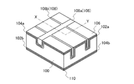
本発明の一態様における光電変換装置の斜視図の一例を図1に示す。なお、図1は断面の
構成をわかりやすく説明するために、光電変換装置の一部を切り出した図となっている。
FIG. 1 illustrates an example of a perspective view of a photoelectric conversion device according to one embodiment of the present invention. Note that FIG. 1 is a diagram in which a part of the photoelectric conversion device is cut out in order to easily understand the cross-sectional configuration.
図1に示す光電変換装置は、結晶性シリコン基板100に接する第1のシリコン半導体層
102a及び第3のシリコン半導体層102b、第1のシリコン半導体層102a及び第
3のシリコン半導体層102bと接する第2のシリコン半導体層104a及び第4のシリ
コン半導体層104b、第2のシリコン半導体層104aと接する透光性導電膜106、
該透光性導電膜106と接するグリッド電極108、並びに第4のシリコン半導体層10
4bと接する裏面電極110を含んで構成される。なお、グリッド電極108が形成され
た面側が受光面となる。
The photoelectric conversion device illustrated in FIG. 1 includes a first
It is configured to include a
第1のシリコン半導体層102a及び第3のシリコン半導体層102bは、水素を含み、
欠陥が少ない高品質なi型半導体層であり、結晶性シリコン基板100の表面欠陥を終端
することができ、光電変換層における少数キャリアの再結合を低減し、少数キャリアのラ
イフタイムを長くすることができる。
The first
A high-quality i-type semiconductor layer with few defects, capable of terminating surface defects of the
なお、本明細書において、i型の半導体とは、フェルミ準位がバンドギャップの中央に位
置する所謂真性半導体の他、半導体に含まれるp型若しくはn型を付与する不純物が1×
1020atoms/cm3以下の濃度であり、暗伝導度に対して光伝導度が高い半導体
を指す。例えば、第1のシリコン半導体層102a及び第3のシリコン半導体層102b
には、プラズマCVD法等で形成される非晶質シリコン半導体を用いることができる。
Note that in this specification, an i-type semiconductor means a so-called intrinsic semiconductor in which the Fermi level is located in the center of the band gap, and an impurity imparting p-type or n-type contained in the semiconductor is 1 ×.
A semiconductor having a concentration of 10 20 atoms / cm 3 or less and high photoconductivity with respect to dark conductivity. For example, the first
For this, an amorphous silicon semiconductor formed by a plasma CVD method or the like can be used.
なお、本明細書において光電変換層とは、光電変換に大きく寄与する半導体領域を意味す
るものである。本実施の形態においては、結晶性シリコン基板100及び該結晶性シリコ
ンに接する第1のシリコン半導体層102a及び第3のシリコン半導体層102bが該当
する。
In the present specification, the photoelectric conversion layer means a semiconductor region that greatly contributes to photoelectric conversion. In this embodiment mode, the
第2のシリコン半導体層104a及び第4のシリコン半導体層104bは、内部電界形成
層であり、一方がp型半導体層、他方がn型半導体層で形成される。該半導体層は、例え
ば、導電型を付与する不純物を含む非晶質シリコン層や微結晶シリコン層で形成すること
ができる。
The second
結晶性シリコン基板100には交差するように溝部が形成されており、該溝部には第1の
シリコン半導体層102a、第2のシリコン半導体層104a、透光性導電膜106、及
びグリッド電極108が埋め込まれている。なお、グリッド電極108の線幅の広い領域
がバスバー電極108a、線幅の狭い領域がフィンガー電極108bである。
A groove portion is formed in the
グリッド電極108を埋め込み型とすることで、高アスペクト比の電極を形成することが
でき、グリッド電極108の微細化にともなう抵抗の増加を抑制することができる。すな
わち、グリッド電極108の微細化による弊害(抵抗増)をともなわず、受光面積を増加
することができ、光電変換装置の変換効率を向上させることができる。
By making the
なお、本発明の一態様における光電変換装置は、図1の構成に限らず、図2に示す構成で
あってもよい。図2の光電変換装置は、図1の構成とはグリッド電極108と透光性導電
膜106の積層順序が異なるものであり、受光面側の表面全体に透光性導電膜106を有
している。このような構成は、図1の構成において、溝部の壁面に対する透光性導電膜の
被覆性が十分でないときに有効であり、グリッド電極108と透光性導電膜106との接
触状態を良好にすることができる。
Note that the photoelectric conversion device according to one embodiment of the present invention is not limited to the configuration in FIG. 1 and may have a configuration illustrated in FIG. The photoelectric conversion device in FIG. 2 is different from the structure in FIG. 1 in the order of stacking the
以下に図1に示した光電変換装置の作製方法について図3を用いて説明する。なお、図3
は、図1に示すX−Yの線分下の断面に相当する断面図である。
A method for manufacturing the photoelectric conversion device illustrated in FIG. 1 is described below with reference to FIGS. Note that FIG.
FIG. 2 is a cross-sectional view corresponding to a cross section under the line XY shown in FIG. 1.
本発明の一態様に用いることのできる結晶性シリコン基板には、単結晶シリコン基板や多
結晶シリコン基板を用いることができる。これらの結晶性シリコン基板の導電型や製造方
法は、特に限定されない。本実施の形態においては、MCZ(Magnetic Czo
chralski)法で製造されたn型の単結晶シリコン基板を用いる。
As the crystalline silicon substrate that can be used in one embodiment of the present invention, a single crystal silicon substrate or a polycrystalline silicon substrate can be used. The conductivity type and manufacturing method of these crystalline silicon substrates are not particularly limited. In the present embodiment, MCZ (Magnetic Czo
The n-type single crystal silicon substrate manufactured by the chalski method is used.
まず、結晶性シリコン基板100に第1の溝部210、第2の溝部220を形成する(図
3(A)参照)。該溝部は、ダイシング加工、またはレーザ加工で形成することができる
。図3(A)における溝部は、ダイシング加工を用いた場合の形状(矩形型)を示してい
るが、V字型であってもよい。レーザ加工を行った場合には、V字型となりやすい。また
、周囲がV字型に加工されたダイシングブレードを用いれば、ダイシング加工でも溝部の
底部をV字型とすることができる。
First, the
なお、レーザ加工を行う場合は、YAGレーザの基本波(波長1064nm)、第2高調
波(波長532nm)、第3高調波(波長355nm)、第4高調波(波長266nm)
などを用い、ビーム径、出力及び走査速度を調整して所望の形状の溝部を形成することが
できる。例えば、YAGレーザの第3高調波で、ビーム径φ20μm、パワー密度160
kW/cm2、走査速度0.1cm/secで単結晶シリコン基板の加工を行うと、幅3
0乃至40μm、深さ40乃至70μmの溝部を形成することができる。
When laser processing is performed, the fundamental wave (wavelength 1064 nm), second harmonic (wavelength 532 nm), third harmonic (wavelength 355 nm), and fourth harmonic (wavelength 266 nm) of the YAG laser.
Etc. can be used to adjust the beam diameter, output and scanning speed to form a groove of a desired shape. For example, the third harmonic of a YAG laser, a beam diameter of 20 μm, and a power density of 160
When a single crystal silicon substrate is processed at kW / cm 2 and a scanning speed of 0.1 cm / sec, a width of 3
Grooves having a depth of 0 to 40 μm and a depth of 40 to 70 μm can be formed.
第1の溝部210は、バスバー電極を埋め込むための溝であり、0.1mm以上2.0m
m以下、好ましくは0.25mm以上1.5mm以下、更に好ましくは0.5mm以上1
.0mm以下の幅とする。該溝部の幅は、バスバー電極として必要な抵抗を考慮するだけ
でなく、後述する導電性樹脂の注入工程を困難にさせることのない幅で形成する。
The
m or less, preferably 0.25 mm or more and 1.5 mm or less, more preferably 0.5 mm or more and 1
. The width is 0 mm or less. The width of the groove portion is not limited in consideration of the resistance necessary for the bus bar electrode, but is formed so as not to make the conductive resin injection process described later difficult.
第2の溝部220は、フィンガー電極を埋め込むための溝であり、0.01mm以上0.
1mm以下、好ましくは0.01mm以上0.08mm以下、更に好ましくは0.01m
m以上0.06mm以下の幅とする。該溝部の幅は、フィンガー電極として必要な抵抗を
考慮するだけでなく、後述する導電性樹脂の注入に必要な毛細管現象が十分に発現する幅
で形成する。
The
1 mm or less, preferably 0.01 mm or more and 0.08 mm or less, more preferably 0.01 m
The width is from m to 0.06 mm. The width of the groove is not limited in consideration of the resistance necessary for the finger electrode, but is formed with a width that sufficiently exhibits the capillary phenomenon necessary for injecting the conductive resin described later.
なお、図3(A)では第1の溝部210を浅く、第2の溝部220を深く形成する構造を
図示しているが、これに限らず第1の溝部210の方を深く形成する構造や、両者を同一
の深さで形成する構造であっても良い。ただし、基板の強度を考慮すると、溝部の深さは
基板厚の2/3、好ましくは1/2を上限とすることが好ましい。溝部が深すぎると、基
板の強度が保てなくなり、工程途中での破損が起きる場合や、製品の強度を低下させ、信
頼性を悪化させる場合がある。例えば、基板厚が0.5mmの場合、溝部の深さは、約0
.25mmから約0.35mmを上限とすることが好ましい。
Note that FIG. 3A illustrates a structure in which the
. The upper limit is preferably from 25 mm to about 0.35 mm.
次いで、第1の溝部210及び第2の溝部220の表層に発生したダメージ層をエッチン
グ工程にて取り除く。エッチングには、例えば、酢酸、弗酸、硝酸を含むエッチング液を
用いることができる。該エッチング液は、それぞれの酸の比率を調整することでダメージ
層を優先的にエッチングすることができる。また、アルカリ性のエッチング液を使用して
、結晶性シリコン基板100表面をエッチングすると同時にテクスチャを形成しても良い
。テクスチャを形成することによって、反射防止または光閉じ込め効果を光電変換装置に
付与することができる。なお、このエッチング工程は省くこともできる。
Next, the damaged layer generated on the surface layer of the
次いで、結晶性シリコン基板100の溝部を形成した面にプラズマCVD法を用いて第1
のシリコン半導体層102aを形成する。第1のシリコン半導体層102aの厚さは、3
nm以上50nm以下とすることが好ましい。本実施の形態において、第1のシリコン半
導体層102aはi型の非晶質シリコンであり、膜厚は5nmとする。
Next, a first surface is formed on the surface of the
The
It is preferable to set it to 50 nm or more. In this embodiment, the first
例えば、第1のシリコン半導体層102aの成膜条件は、反応室に流量5sccm以上2
00sccm以下のモノシランガスを導入し、反応室内の圧力を10Pa以上100Pa
以下、電極間隔を15mm以上40mm以下、電力密度を8mW/cm2以上50mW/
cm2以下とすればよい。
For example, the film formation condition of the first
A monosilane gas of 00 sccm or less is introduced, and the pressure in the reaction chamber is set to 10 Pa or more and 100 Pa.
Hereinafter, the electrode interval is 15 mm to 40 mm, and the power density is 8 mW / cm 2 to 50 mW /
What is necessary is just to set it as cm < 2 > or less.
次いで、第1のシリコン半導体層102a上に第2のシリコン半導体層104aを形成す
る。第2のシリコン半導体層104aの厚さは3nm以上50nm以下とすることが好ま
しい。本実施の形態において、第2のシリコン半導体層104aはp型の微結晶シリコン
であり、膜厚は10nmとする。なお、第2のシリコン半導体層104aに、p型の非晶
質シリコンを用いてもよい。
Next, a second
例えば、第2のシリコン半導体層104aの成膜条件は、反応室に流量1sccm以上1
0sccm以下のモノシランガス、流量100sccm以上5000sccm以下の水素
、流量5sccm以上50sccm以下の水素ベースのジボラン(0.1%)を導入し、
反応室内の圧力を450Pa以上100000Pa以下、好ましくは2000Pa以上5
0000Pa以下とし、電極間隔を8mm以上30mm以下とし、電力密度を200mW
/cm2以上1500mW/cm2以下とすればよい。
For example, the film formation condition of the second
Introducing monosilane gas of 0 sccm or less, hydrogen of
The pressure in the reaction chamber is 450 Pa to 100000 Pa, preferably 2000 Pa to 5
0000 Pa or less, electrode spacing is 8 mm or more and 30 mm or less, and power density is 200 mW.
/ Cm 2 or more and 1500 mW / cm 2 or less.
次いで、結晶性シリコン基板100の他方の面にプラズマCVD法を用いて第3のシリコ
ン半導体層102bを形成する。第3のシリコン半導体層102bの厚さは、3nm以上
50nm以下とすることが好ましく、本実施の形態において、第3のシリコン半導体層1
02bはi型であり、膜厚は5nmとする。なお、第3のシリコン半導体層102bは、
第1のシリコン半導体層102aと同様の成膜条件にて形成することができる。
Next, a third
02b is i-type and the film thickness is 5 nm. Note that the third
It can be formed under the same film formation conditions as the first
次いで、第3のシリコン半導体層102b上に第4のシリコン半導体層104bを形成す
る。第4のシリコン半導体層104bの厚さは3nm以上50nm以下とすることが好ま
しい。本実施の形態において、第4のシリコン半導体層104bはn型の微結晶シリコン
であり、膜厚は10nmとする。なお、第4のシリコン半導体層104bに、n型の非晶
質シリコンを用いてもよい。
Next, a fourth
例えば、第4のシリコン半導体層104bの成膜条件は、反応室に流量1sccm以上1
0sccm以下のモノシランガス、流量100sccm以上5000sccm以下の水素
、流量5sccm以上50sccm以下の水素ベースのホスフィン(0.5%)を導入し
、反応室内の圧力を450Pa以上100000Pa以下、好ましくは2000Pa以上
50000Pa以下とし、電極間隔を8mm以上30mm以下とし、電力密度を200m
W/cm2以上1500mW/cm2以下とすればよい。
For example, the deposition condition of the fourth
Monosilane gas of 0 sccm or less, hydrogen with a flow rate of 100 sccm or more and 5000 sccm or less, hydrogen-based phosphine (0.5%) with a flow rate of 5 sccm or more and 50 sccm or less are introduced, and the pressure in the reaction chamber is set to 450 Pa to 100000 Pa, preferably 2000 Pa to 50000 Pa. The electrode spacing is 8 mm or more and 30 mm or less, and the power density is 200 m.
W / cm 2 or more and 1500 mW / cm 2 or less may be used.
なお、本実施の形態において、上記非晶質シリコン層及び微結晶シリコン層の成膜に用い
る電源には周波数13.56MHzのRF電源を用いるが、27.12MHz、60MH
z、または100MHzのRF電源を用いても良い。また、連続放電だけでなく、パルス
放電にて成膜を行っても良い。パルス放電を行うことで、膜質の向上や気相中で発生する
パーティクルを低減することができる。
Note that in this embodiment mode, an RF power source having a frequency of 13.56 MHz is used as a power source for forming the amorphous silicon layer and the microcrystalline silicon layer, but 27.12 MHz and 60 MH are used.
An RF power source of z or 100 MHz may be used. Further, film formation may be performed not only by continuous discharge but also by pulse discharge. By performing pulse discharge, film quality can be improved and particles generated in the gas phase can be reduced.
次いで、第2のシリコン半導体層104a上に透光性導電膜106を形成する。透光性導
電膜106には、例えば、インジウム錫酸化物、珪素を含むインジウム錫酸化物、亜鉛を
含む酸化インジウム、酸化亜鉛、ガリウムを含む酸化亜鉛、アルミニウムを含む酸化亜鉛
、酸化錫、フッ素を含む酸化錫、またはアンチモンを含む酸化錫等を用いることができる
。また、透光性導電膜106は単層に限らず、異なる膜の積層でも良い。例えば、インジ
ウム錫酸化物とアルミニウムを含む酸化亜鉛の積層や、インジウム錫酸化物とフッ素を含
む酸化錫の積層などを用いることができる。膜厚は総厚で10nm以上1000nm以下
とする。また、透光性導電膜106の表面をテクスチャ構造としても良い。
Next, a light-transmitting
次いで、第4のシリコン半導体層104b上に裏面電極110を形成する(図3(B)参
照)。裏面電極110には、銀、アルミニウム、銅などの低抵抗金属を用いることができ
、スパッタ法や真空蒸着法などで形成することができる。または、スクリーン印刷法を用
いて、銀ペーストや、銅ペーストなどの導電性樹脂で形成しても良い。
Next, the
なお、結晶性シリコン基板100の表裏に設ける膜の形成は、上記に示した順序に限らず
、図3(B)に示した構造が形成できればよい。例えば、第1のシリコン半導体層102
aの形成し、その次に第3のシリコン半導体層102bを形成しても良い。
Note that the formation of the films provided on the front and back surfaces of the
a may be formed, and then the third
次いで、第1の溝部210及び第2の溝部220において、透光性導電膜106と接する
ように導電性樹脂を注入し、グリッド電極108を形成する(図3(C)参照)。このグ
リッド電極108の形成方法について、図4を用いて詳細を説明する。
Next, conductive resin is injected into the
図4は、導電性樹脂をバスバー電極となる第1の溝部210、及びフィンガー電極となる
第2の溝部220に注入する様子を示すものである。まず、導電性樹脂を第1の溝部21
0に適当量を注入する(図中の実線矢印)。該導電性樹脂の注入にはディスペンス法を用
いる。また、インクジェット法を用いても良い。
FIG. 4 shows a state in which conductive resin is injected into the
An appropriate amount is injected into 0 (solid arrow in the figure). A dispensing method is used for injecting the conductive resin. Further, an ink jet method may be used.
第1の溝部210と第2の溝部220は、交差してつながっているため、第1の溝部21
0に注入した導電性樹脂は、図中の点線矢印で示す方向に入り込み、第2の溝部220に
注入される。このとき、第2の溝部は、0.01mm以上0.1mm以下の幅で形成され
ているため、毛細管現象が発現し、第2の溝部に容易に導電性樹脂を注入することができ
る。
Since the
The conductive resin injected into 0 enters the direction indicated by the dotted arrow in the figure and is injected into the
この方法による該溝部への導電性樹脂の注入は、溝部の一方の端部から水平方向に溝部を
充填するように行われるため、溝部の内部に気泡が残ることがなく、溝部に導電性樹脂を
密に充填することができる。なお、導電性樹脂は焼成後に体積変化することがあるため、
導電性樹脂の溝部への注入及び焼成を複数回繰り返しても良い。また、結晶性シリコン基
板100に超音波振動を加え、導電性樹脂の溝部への注入を促進させても良い。
The injection of the conductive resin into the groove portion by this method is performed so as to fill the groove portion in the horizontal direction from one end portion of the groove portion, so that no bubbles remain in the groove portion, and the conductive resin is left in the groove portion. Can be packed tightly. In addition, since the conductive resin may change in volume after firing,
The injection and baking of the conductive resin into the groove may be repeated a plurality of times. In addition, ultrasonic vibration may be applied to the
導電性樹脂には、銀、金、銀−パラジウム、銅などをフィラーとして含むものを用いるこ
とができ、抵抗が低く、比較的低コストの銀をフィラーとして含むものが好ましい。また
、フィラーには、フィラーサイズが5nm乃至100nmの所謂ナノ粒子と呼ばれるもの
を用いることが特に好ましい。導電性樹脂の溶媒には水系溶媒、炭化水素系溶媒、ケトン
系溶媒などを用いることができる。また、導電性樹脂の粘度は、100mPa・s以下、
好ましくは10mPa・s、更に好ましくは1mPa・sとする。粘度の低いものほど溝
部への注入を容易に行うことができる。また、第1のシリコン半導体層102a及び第3
のシリコン半導体層102bの膜質を変質させないように、導電性樹脂は低温で焼成でき
る熱硬化型であることが好ましい。例えば、300℃以下、好ましくは250℃以下で焼
成できるものを用いる。
As the conductive resin, a resin containing silver, gold, silver-palladium, copper, or the like as a filler can be used, and a resin having low resistance and relatively low cost silver as a filler is preferable. Further, as the filler, it is particularly preferable to use what is called nanoparticles having a filler size of 5 nm to 100 nm. As the solvent for the conductive resin, an aqueous solvent, a hydrocarbon solvent, a ketone solvent, or the like can be used. The viscosity of the conductive resin is 100 mPa · s or less,
It is preferably 10 mPa · s, more preferably 1 mPa · s. The lower the viscosity, the easier the injection into the groove. The first
The conductive resin is preferably of a thermosetting type that can be fired at a low temperature so as not to change the film quality of the
なお、毛細管現象により溝部に導電性樹脂が注入される水平方向の距離は、第2の溝部2
20の幅によって異なり、幅を狭くするほど該距離を延ばすことができる。また、第2の
溝部の深さも深いほど該距離を延ばすことができる。図5は、単結晶シリコン基板に幅0
.1mmで、0.03mm乃至0.2mmの深さの溝部を形成し、溝部の端部に銀のナノ
粒子を含む導電性樹脂(水系溶媒、粘度15mPa・s)を滴下し、その水平方向の注入
距離を調べたものである。溝部の深さが深いほど注入距離は長くなり、溝部の深さが0.
2mmの場合は、約30mmの注入距離が得られる。これは、10cm角以上のセルであ
っても2本のバスバー電極を設ければ十分に対応できることを示している。
The horizontal distance at which the conductive resin is injected into the groove by capillary action is the second groove 2.
The distance can be increased as the width is reduced. Further, the distance can be extended as the depth of the second groove portion is increased. FIG. 5 shows a single crystal silicon substrate with a width of 0.
. 1 mm, a groove part having a depth of 0.03 mm to 0.2 mm is formed, and a conductive resin (aqueous solvent,
In the case of 2 mm, an injection distance of about 30 mm is obtained. This indicates that even a cell of 10 cm square or more can be sufficiently handled by providing two bus bar electrodes.
なお、第1の溝部210及び第2の溝部220をレーザ加工によって形成する場合は、結
晶性シリコン基板100の端部より内側の領域を選択的に加工して溝部を形成することが
できるが、ダイシング加工では、結晶性シリコン基板100の端部まで溝部が形成されて
しまう。従って、ダイシング加工で第1の溝部210及び第2の溝部220を形成した場
合は、導電性樹脂を注入する際に、第1の溝部210の端部、または第2の溝部220の
端部から導電性樹脂が漏出しない構造とすることが好ましい。
Note that in the case where the
例えば、図6に示すように結晶性シリコン基板100の端部近傍に壁部300を設けるこ
とが好ましい。図6(A)は、第1の溝部210及び第2の溝部220を形成後に壁部3
00を形成した状態の平面図である。壁部300は、結晶性シリコン基板100の端部近
傍の溝部を絶縁樹脂または導電性樹脂で充填するようにディスペンス法等で形成する。な
お、図6(A)では、溝部でない領域にも壁部300を形成するように図示してあるが、
溝部のみを選択的に充填するように形成してもよい。ここで、壁部300の形成に用いる
絶縁樹脂または導電性樹脂には、第2の溝部220において、毛細管現象によって水平方
向に注入されないように粘度の高い樹脂を用いることが好ましい。
For example, it is preferable to provide a
It is a top view in the state where 00 was formed. The
You may form so that only a groove part may be filled up selectively. Here, as the insulating resin or conductive resin used for forming the
壁部300を形成した後に、上述した方法によって導電性樹脂を注入し、図6(B)に示
すような壁部300より内側にグリッド電極108が形成された構造を得ることができる
。なお、壁部300の下側にフィンガー電極108bよりも深い溝を設けても良い。該溝
を設けることでキャリアライフタイムの短い結晶性シリコン基板100の端部を分離する
ことができ、光電変換層の特性を向上させることができる。
After the
また、図7に示すように、第1の溝部210及び第2の溝部220、またはどちらか一方
に金属ワイヤー400を埋め込んだ構成としてもよい。導電性樹脂は金属よりも抵抗が高
いため、金属ワイヤー400と導電性樹脂の両方で埋め込み電極を形成することで、更に
低抵抗のグリッド電極108を形成することができる。また、溝部に金属ワイヤーを入れ
ることで毛細管現象を更に起こしやすくする効果を得ることもできる。なお、金属ワイヤ
ー400には銀や銅などの低抵抗金属材料で形成されたものが適しており、単線であって
も撚り線であってもよい。
Moreover, as shown in FIG. 7, it is good also as a structure which embedded the
以上により、短軸方向の断面においてアスペクト比の高い埋め込み電極を形成することが
でき、電気特性が向上した光電変換装置を提供することができる。なお、図2の光電変換
装置は、上記の作製方法において、透光性導電膜とグリッド電極となる導電性樹脂の形成
順序を逆にすることで形成することができる。
As described above, a buried electrode with a high aspect ratio can be formed in the cross section in the minor axis direction, and a photoelectric conversion device with improved electrical characteristics can be provided. Note that the photoelectric conversion device in FIG. 2 can be formed by reversing the formation order of the light-transmitting conductive film and the conductive resin to be the grid electrode in the above manufacturing method.
100 結晶性シリコン基板
102a 第1のシリコン半導体層
102b 第3のシリコン半導体層
104a 第2のシリコン半導体層
104b 第4のシリコン半導体層
106 透光性導電膜
108 グリッド電極
108a バスバー電極
108b フィンガー電極
110 裏面電極
210 第1の溝部
220 第2の溝部
300 壁部
400 金属ワイヤー
100
Claims (4)
前記第1の溝部上、前記第2の溝部上、及び前記結晶性シリコン基板の前記一方の面上に、第1のシリコン半導体層を形成し、
前記第1のシリコン半導体層上に、一導電型を有する第2のシリコン半導体層を形成し、
前記結晶性シリコン基板の他方の面上に、第3のシリコン半導体層を形成し、
前記第3のシリコン半導体層上に、前記一導電型とは逆の導電型を有する第4のシリコン半導体層を形成し、
前記第2のシリコン半導体層上に透光性導電膜を形成し、
前記第4のシリコン半導体層上に裏面電極を形成し、
前記第1のシリコン半導体層、前記第2のシリコン半導体層、及び前記透光性導電膜が積層された前記第1の溝部の一方の端部から、水平方向にもう一方の端部に向かって、前記第1の溝部を充填するように導電性樹脂を注入し、
毛細管現象を利用して、前記第1の溝部から前記第2の溝部に前記導電性樹脂を注入し、
前記導電性樹脂を焼成して、埋め込み型のグリッド電極を形成し、
前記第2の溝部は、前記第1の溝部よりも幅が狭く、且つ深さが深く形成され、
前記第2の溝部の幅は、0.01mm以上0.1mm以下であり、
前記第1の溝部に前記導電性樹脂を注入する工程、及び、前記第2の溝部に前記導電性樹脂を注入する工程において、前記結晶性シリコン基板に超音波振動を加えることを特徴とする光電変換装置の作製方法。 On one surface of the crystalline silicon substrate, forming a first groove and a second groove having a region intersecting with the first groove,
The first on the groove, the second on the groove, and the on one surface of the crystalline silicon substrate, forming a first silicon semiconductor layer,
The first silicon semiconductor layer, forming a second silicon semiconductor layer having one conductivity type,
On the other surface of the crystalline silicon substrate, forming a third silicon semiconductor layer,
The third silicon semiconductor layer, forming a fourth silicon semiconductor layer having a conductivity type opposite to said one conductivity type,
Forming a translucent conductive film on the second silicon semiconductor layer;
The back surface electrode is formed on the fourth silicon semiconductor layer,
From one end of the first groove where the first silicon semiconductor layer, the second silicon semiconductor layer, and the translucent conductive film are stacked , toward the other end in the horizontal direction. , Injecting a conductive resin so as to fill the first groove,
Utilizing capillary action, the conductive resin is injected from the first groove portion to the second groove portion ,
And sintering the conductive resin to form an embedded grid electrode,
The second groove is narrower and deeper than the first groove,
The width of the second groove is 0.01 mm or more and 0.1 mm or less,
In the step of injecting the conductive resin into the first groove and the step of injecting the conductive resin into the second groove, an ultrasonic vibration is applied to the crystalline silicon substrate. A method for manufacturing a conversion device.
前記結晶性シリコン基板の一方の面上に、前記結晶性シリコン基板の端部に沿うように、少なくとも一以上の第3の溝部を形成し、Forming at least one or more third grooves on one surface of the crystalline silicon substrate along the edge of the crystalline silicon substrate;
前記第3の溝部に、絶縁性樹脂又は導電性樹脂を注入し、Insulating resin or conductive resin into the third groove,
前記第1の溝部上、前記第2の溝部上、及び前記結晶性シリコン基板の前記一方の面上に、第1のシリコン半導体層を形成し、Forming a first silicon semiconductor layer on the first groove, on the second groove, and on the one surface of the crystalline silicon substrate;
前記第1のシリコン半導体層上に、一導電型を有する第2のシリコン半導体層を形成し、Forming a second silicon semiconductor layer having one conductivity type on the first silicon semiconductor layer;
前記結晶性シリコン基板の他方の面上に、第3のシリコン半導体層を形成し、Forming a third silicon semiconductor layer on the other surface of the crystalline silicon substrate;
前記第3のシリコン半導体層上に、前記一導電型とは逆の導電型を有する第4のシリコン半導体層を形成し、Forming a fourth silicon semiconductor layer having a conductivity type opposite to the one conductivity type on the third silicon semiconductor layer;
前記第2のシリコン半導体層上に透光性導電膜を形成し、Forming a translucent conductive film on the second silicon semiconductor layer;
前記第4のシリコン半導体層上に裏面電極を形成し、Forming a back electrode on the fourth silicon semiconductor layer;
前記第1のシリコン半導体層、前記第2のシリコン半導体層、及び前記透光性導電膜が積層された前記第1の溝部の一方の端部から、水平方向にもう一方の端部に向かって、前記第1の溝部を充填するように導電性樹脂を注入し、From one end of the first groove where the first silicon semiconductor layer, the second silicon semiconductor layer, and the translucent conductive film are stacked, toward the other end in the horizontal direction. , Injecting a conductive resin so as to fill the first groove,
毛細管現象を利用して、前記第1の溝部から前記第2の溝部に前記導電性樹脂を注入し、Utilizing capillary action, the conductive resin is injected from the first groove portion to the second groove portion,
前記導電性樹脂を焼成して、埋め込み型のグリッド電極を形成し、Firing the conductive resin to form an embedded grid electrode,
前記第2の溝部は、前記第1の溝部よりも幅が狭く、且つ深さが深く形成され、The second groove is narrower and deeper than the first groove,
前記第2の溝部の幅は、0.01mm以上0.1mm以下であり、The width of the second groove is 0.01 mm or more and 0.1 mm or less,
前記第1の溝部に前記導電性樹脂を注入する工程、及び、前記第2の溝部に前記導電性樹脂を注入する工程において、前記結晶性シリコン基板に超音波振動を加え、In the step of injecting the conductive resin into the first groove portion and the step of injecting the conductive resin into the second groove portion, ultrasonic vibration is applied to the crystalline silicon substrate,
前記第3の溝部に注入される絶縁性樹脂の粘度又は前記第3の溝部に注入される導電性樹脂の粘度は、前記第1の溝部に注入される前記導電性樹脂の粘度よりも高いことを特徴とする光電変換装置の作製方法。The viscosity of the insulating resin injected into the third groove or the viscosity of the conductive resin injected into the third groove is higher than the viscosity of the conductive resin injected into the first groove. And a method for manufacturing a photoelectric conversion device.
前記第1のシリコン半導体層の導電型はi型であり、
前記第2のシリコン半導体層の導電型はp型又はn型であることを特徴とする光電変換装置の作製方法。 In claim 1 or 2 ,
The conductivity type of the first silicon semiconductor layer is i-type,
A method for manufacturing a photoelectric conversion device , wherein the conductivity type of the second silicon semiconductor layer is p-type or n-type.
前記第1の溝部に注入される導電性樹脂は、銀、金、銀−パラジウム、又は銅をフィラーとして含むことを特徴とする光電変換装置の作製方法。The method for manufacturing a photoelectric conversion device, wherein the conductive resin injected into the first groove includes silver, gold, silver-palladium, or copper as a filler.
Applications Claiming Priority (2)
| Application Number | Priority Date | Filing Date | Title |
|---|---|---|---|
| JP2010263337 | 2010-11-26 | ||
| JP2010263337 | 2010-11-26 |
Related Parent Applications (1)
| Application Number | Title | Priority Date | Filing Date |
|---|---|---|---|
| JP2011256925A Division JP2012129518A (en) | 2010-11-26 | 2011-11-25 | Photoelectric conversion device, and method for manufacturing the same |
Publications (2)
| Publication Number | Publication Date |
|---|---|
| JP2016122851A JP2016122851A (en) | 2016-07-07 |
| JP6101376B2 true JP6101376B2 (en) | 2017-03-22 |
Family
ID=46125824
Family Applications (2)
| Application Number | Title | Priority Date | Filing Date |
|---|---|---|---|
| JP2011256925A Withdrawn JP2012129518A (en) | 2010-11-26 | 2011-11-25 | Photoelectric conversion device, and method for manufacturing the same |
| JP2016021809A Expired - Fee Related JP6101376B2 (en) | 2010-11-26 | 2016-02-08 | Method for manufacturing photoelectric conversion device |
Family Applications Before (1)
| Application Number | Title | Priority Date | Filing Date |
|---|---|---|---|
| JP2011256925A Withdrawn JP2012129518A (en) | 2010-11-26 | 2011-11-25 | Photoelectric conversion device, and method for manufacturing the same |
Country Status (2)
| Country | Link |
|---|---|
| US (1) | US9337361B2 (en) |
| JP (2) | JP2012129518A (en) |
Families Citing this family (8)
| Publication number | Priority date | Publication date | Assignee | Title |
|---|---|---|---|---|
| JP6004946B2 (en) * | 2013-01-08 | 2016-10-12 | 三菱電機株式会社 | Solar cell and solar cell module |
| KR101400206B1 (en) * | 2013-11-20 | 2014-05-28 | 주식회사 이건창호 | Method for manufacturing solar cell structure for thermal insulation |
| CN104091858B (en) * | 2014-07-28 | 2017-11-07 | 六安市大宇高分子材料有限公司 | A kind of manufacture method of selective emitter solar battery |
| KR101875741B1 (en) * | 2017-01-06 | 2018-07-06 | 엘지전자 주식회사 | Solar cell and method for manufacturing the same |
| CN112736148B (en) * | 2020-12-03 | 2023-07-14 | 圣晖莱南京能源科技有限公司 | Flexible CIGS thin film battery with high photoelectric conversion efficiency |
| CN112993062B (en) * | 2020-12-03 | 2023-07-25 | 圣晖莱南京能源科技有限公司 | Flexible CIGS thin film battery with embedded grid line electrode |
| CN114759101B (en) * | 2020-12-29 | 2023-08-01 | 隆基绿能科技股份有限公司 | Hot carrier solar cell and photovoltaic module |
| CN116918079A (en) * | 2022-01-27 | 2023-10-20 | 凯盛科技集团有限公司 | Method for forming cross wires of thin film solar cell module |
Family Cites Families (22)
| Publication number | Priority date | Publication date | Assignee | Title |
|---|---|---|---|---|
| JP2992464B2 (en) * | 1994-11-04 | 1999-12-20 | キヤノン株式会社 | Covering wire for current collecting electrode, photovoltaic element using the covering wire for current collecting electrode, and method of manufacturing the same |
| JP2000188414A (en) | 1998-12-24 | 2000-07-04 | Sanyo Electric Co Ltd | Solar battery element and its manufacture |
| JP5008216B2 (en) | 2000-10-13 | 2012-08-22 | 株式会社アルバック | Inkjet ink manufacturing method |
| JP2003031831A (en) | 2001-07-13 | 2003-01-31 | Sanyo Electric Co Ltd | Photovoltaic element and its manufacturing method |
| JP2004281813A (en) | 2003-03-17 | 2004-10-07 | Ebara Corp | Manufacturing method for solar cell |
| US20050189013A1 (en) * | 2003-12-23 | 2005-09-01 | Oliver Hartley | Process for manufacturing photovoltaic cells |
| ES2365904T3 (en) * | 2004-01-13 | 2011-10-13 | Sanyo Electric Co., Ltd. | PHOTOVOLTAIC DEVICE. |
| JP4526902B2 (en) | 2004-08-13 | 2010-08-18 | 信越半導体株式会社 | Manufacturing method of solar cell |
| JP4222992B2 (en) * | 2004-09-29 | 2009-02-12 | 三洋電機株式会社 | Photovoltaic device |
| US7554031B2 (en) * | 2005-03-03 | 2009-06-30 | Sunpower Corporation | Preventing harmful polarization of solar cells |
| JP4993870B2 (en) | 2005-03-31 | 2012-08-08 | 三洋電機株式会社 | Photovoltaic element and manufacturing method thereof |
| US8344238B2 (en) * | 2005-07-19 | 2013-01-01 | Solyndra Llc | Self-cleaning protective coatings for use with photovoltaic cells |
| JP2007173507A (en) * | 2005-12-22 | 2007-07-05 | Sanyo Electric Co Ltd | Method and unit for fabricating a photovoltaic device |
| JP4337001B2 (en) | 2007-07-11 | 2009-09-30 | 智雄 松下 | Conductive pattern forming method, conductive pattern forming apparatus, and substrate for solar cell |
| JP5380810B2 (en) * | 2007-09-28 | 2014-01-08 | 三洋電機株式会社 | Solar cell module |
| JP5172480B2 (en) | 2008-06-04 | 2013-03-27 | シャープ株式会社 | Photoelectric conversion device and manufacturing method thereof |
| JP5368022B2 (en) | 2008-07-17 | 2013-12-18 | 信越化学工業株式会社 | Solar cell |
| KR20100013649A (en) * | 2008-07-31 | 2010-02-10 | 삼성전자주식회사 | Photovoltaic device and method of manufacturing the same |
| US20100154874A1 (en) | 2008-09-29 | 2010-06-24 | Takashi Hirose | Photoelectric conversion device and manufacturing method thereof |
| JP5178489B2 (en) | 2008-12-17 | 2013-04-10 | 三洋電機株式会社 | Solar cell module and manufacturing method thereof |
| WO2011001842A1 (en) | 2009-07-03 | 2011-01-06 | Semiconductor Energy Laboratory Co., Ltd. | Photoelectric conversion device and manufacturing method thereof |
| US20120305072A1 (en) * | 2009-12-18 | 2012-12-06 | Toray Industries, Inc. | Method for manufacturing semiconductor device and back-contact solar cell |
-
2011
- 2011-11-18 US US13/299,768 patent/US9337361B2/en active Active
- 2011-11-25 JP JP2011256925A patent/JP2012129518A/en not_active Withdrawn
-
2016
- 2016-02-08 JP JP2016021809A patent/JP6101376B2/en not_active Expired - Fee Related
Also Published As
| Publication number | Publication date |
|---|---|
| JP2016122851A (en) | 2016-07-07 |
| US20120132271A1 (en) | 2012-05-31 |
| US9337361B2 (en) | 2016-05-10 |
| JP2012129518A (en) | 2012-07-05 |
Similar Documents
| Publication | Publication Date | Title |
|---|---|---|
| JP6101376B2 (en) | Method for manufacturing photoelectric conversion device | |
| US9871161B2 (en) | Method for making crystalline silicon-based solar cell, and method for making solar cell module | |
| WO2012163517A2 (en) | Solar cell and method for producing same | |
| US9761749B2 (en) | Photoelectric conversion device | |
| WO2016052046A1 (en) | Solar cell, method for manufacturing same, solar cell module, and method for manufacturing same | |
| US9997647B2 (en) | Solar cells and manufacturing method thereof | |
| JP2015191962A (en) | Solar cell and manufacturing method therefor | |
| JP6021392B2 (en) | Method for manufacturing photoelectric conversion device | |
| US9437768B2 (en) | Photoelectric conversion device | |
| JP5745653B2 (en) | Photovoltaic device, manufacturing method thereof, and photovoltaic module | |
| JP3201880U (en) | Solar cell structure with locally deactivated heterojunction | |
| JP2017005270A (en) | Method of manufacturing photoelectric conversion device | |
| JP5917129B2 (en) | Electrode manufacturing method and photoelectric conversion device manufacturing method | |
| KR102049604B1 (en) | Solar cell and Method of manufacturing the same | |
| KR101024322B1 (en) | Method of manufacturing wafer for solar cell, a wafer for solar cell manufactured by the method and method of manufacturing solar cell using the wafer | |
| AU2022205182B1 (en) | Solar cell and production method thereof, photovoltaic module | |
| JP5927028B2 (en) | Photoelectric conversion device | |
| Mai et al. | The development of the advanced semiconductor finger solar cell | |
| JP4215608B2 (en) | Photovoltaic device | |
| JP2009043822A (en) | Method for manufacturing photovoltaic device | |
| JP2005108884A (en) | Process for producing solar cell element |
Legal Events
| Date | Code | Title | Description |
|---|---|---|---|
| A131 | Notification of reasons for refusal |
Free format text: JAPANESE INTERMEDIATE CODE: A131 Effective date: 20161004 |
|
| A521 | Request for written amendment filed |
Free format text: JAPANESE INTERMEDIATE CODE: A523 Effective date: 20161202 |
|
| TRDD | Decision of grant or rejection written | ||
| A01 | Written decision to grant a patent or to grant a registration (utility model) |
Free format text: JAPANESE INTERMEDIATE CODE: A01 Effective date: 20170207 |
|
| A61 | First payment of annual fees (during grant procedure) |
Free format text: JAPANESE INTERMEDIATE CODE: A61 Effective date: 20170224 |
|
| R150 | Certificate of patent or registration of utility model |
Ref document number: 6101376 Country of ref document: JP Free format text: JAPANESE INTERMEDIATE CODE: R150 |
|
| R250 | Receipt of annual fees |
Free format text: JAPANESE INTERMEDIATE CODE: R250 |
|
| R250 | Receipt of annual fees |
Free format text: JAPANESE INTERMEDIATE CODE: R250 |
|
| R250 | Receipt of annual fees |
Free format text: JAPANESE INTERMEDIATE CODE: R250 |
|
| LAPS | Cancellation because of no payment of annual fees |