JP2017005270A - Method of manufacturing photoelectric conversion device - Google Patents
Method of manufacturing photoelectric conversion device Download PDFInfo
- Publication number
- JP2017005270A JP2017005270A JP2016180242A JP2016180242A JP2017005270A JP 2017005270 A JP2017005270 A JP 2017005270A JP 2016180242 A JP2016180242 A JP 2016180242A JP 2016180242 A JP2016180242 A JP 2016180242A JP 2017005270 A JP2017005270 A JP 2017005270A
- Authority
- JP
- Japan
- Prior art keywords
- semiconductor layer
- silicon semiconductor
- single crystal
- silicon substrate
- silicon
- Prior art date
- Legal status (The legal status is an assumption and is not a legal conclusion. Google has not performed a legal analysis and makes no representation as to the accuracy of the status listed.)
- Withdrawn
Links
- 238000006243 chemical reaction Methods 0.000 title claims abstract description 39
- 238000004519 manufacturing process Methods 0.000 title claims description 9
- XUIMIQQOPSSXEZ-UHFFFAOYSA-N Silicon Chemical compound [Si] XUIMIQQOPSSXEZ-UHFFFAOYSA-N 0.000 claims abstract description 163
- 229910052710 silicon Inorganic materials 0.000 claims abstract description 163
- 239000010703 silicon Substances 0.000 claims abstract description 163
- 239000004065 semiconductor Substances 0.000 claims abstract description 149
- 239000000758 substrate Substances 0.000 claims abstract description 123
- 229910021421 monocrystalline silicon Inorganic materials 0.000 claims abstract description 97
- 229910052731 fluorine Inorganic materials 0.000 claims abstract description 34
- YCKRFDGAMUMZLT-UHFFFAOYSA-N Fluorine atom Chemical compound [F] YCKRFDGAMUMZLT-UHFFFAOYSA-N 0.000 claims abstract description 33
- 239000011737 fluorine Substances 0.000 claims abstract description 33
- QVGXLLKOCUKJST-UHFFFAOYSA-N atomic oxygen Chemical compound [O] QVGXLLKOCUKJST-UHFFFAOYSA-N 0.000 claims description 24
- 239000001301 oxygen Substances 0.000 claims description 24
- 229910052760 oxygen Inorganic materials 0.000 claims description 24
- IJGRMHOSHXDMSA-UHFFFAOYSA-N Atomic nitrogen Chemical compound N#N IJGRMHOSHXDMSA-UHFFFAOYSA-N 0.000 claims description 22
- 238000000034 method Methods 0.000 claims description 22
- 229910052757 nitrogen Inorganic materials 0.000 claims description 11
- 238000005268 plasma chemical vapour deposition Methods 0.000 claims description 8
- 230000007547 defect Effects 0.000 abstract description 17
- 238000002161 passivation Methods 0.000 abstract description 6
- 239000010410 layer Substances 0.000 description 109
- 229910021417 amorphous silicon Inorganic materials 0.000 description 22
- 229910021419 crystalline silicon Inorganic materials 0.000 description 18
- 239000012535 impurity Substances 0.000 description 18
- 238000005530 etching Methods 0.000 description 16
- QTBSBXVTEAMEQO-UHFFFAOYSA-N Acetic acid Chemical compound CC(O)=O QTBSBXVTEAMEQO-UHFFFAOYSA-N 0.000 description 15
- KRHYYFGTRYWZRS-UHFFFAOYSA-N Fluorane Chemical compound F KRHYYFGTRYWZRS-UHFFFAOYSA-N 0.000 description 14
- 239000002253 acid Substances 0.000 description 10
- XLOMVQKBTHCTTD-UHFFFAOYSA-N Zinc monoxide Chemical compound [Zn]=O XLOMVQKBTHCTTD-UHFFFAOYSA-N 0.000 description 8
- 238000004140 cleaning Methods 0.000 description 7
- 230000000694 effects Effects 0.000 description 7
- HEMHJVSKTPXQMS-UHFFFAOYSA-M Sodium hydroxide Chemical compound [OH-].[Na+] HEMHJVSKTPXQMS-UHFFFAOYSA-M 0.000 description 6
- 239000000969 carrier Substances 0.000 description 6
- 239000007789 gas Substances 0.000 description 6
- 239000000243 solution Substances 0.000 description 6
- UFHFLCQGNIYNRP-UHFFFAOYSA-N Hydrogen Chemical compound [H][H] UFHFLCQGNIYNRP-UHFFFAOYSA-N 0.000 description 5
- GRYLNZFGIOXLOG-UHFFFAOYSA-N Nitric acid Chemical compound O[N+]([O-])=O GRYLNZFGIOXLOG-UHFFFAOYSA-N 0.000 description 5
- 239000001257 hydrogen Substances 0.000 description 5
- 229910052739 hydrogen Inorganic materials 0.000 description 5
- 229910017604 nitric acid Inorganic materials 0.000 description 5
- RYGMFSIKBFXOCR-UHFFFAOYSA-N Copper Chemical compound [Cu] RYGMFSIKBFXOCR-UHFFFAOYSA-N 0.000 description 4
- KWYUFKZDYYNOTN-UHFFFAOYSA-M Potassium hydroxide Chemical compound [OH-].[K+] KWYUFKZDYYNOTN-UHFFFAOYSA-M 0.000 description 4
- BQCADISMDOOEFD-UHFFFAOYSA-N Silver Chemical compound [Ag] BQCADISMDOOEFD-UHFFFAOYSA-N 0.000 description 4
- 239000012670 alkaline solution Substances 0.000 description 4
- 229910052802 copper Inorganic materials 0.000 description 4
- 239000010949 copper Substances 0.000 description 4
- 239000013078 crystal Substances 0.000 description 4
- 238000009792 diffusion process Methods 0.000 description 4
- AMGQUBHHOARCQH-UHFFFAOYSA-N indium;oxotin Chemical compound [In].[Sn]=O AMGQUBHHOARCQH-UHFFFAOYSA-N 0.000 description 4
- 238000005259 measurement Methods 0.000 description 4
- 230000003287 optical effect Effects 0.000 description 4
- 238000012545 processing Methods 0.000 description 4
- 229910052709 silver Inorganic materials 0.000 description 4
- 239000004332 silver Substances 0.000 description 4
- XOLBLPGZBRYERU-UHFFFAOYSA-N tin dioxide Chemical compound O=[Sn]=O XOLBLPGZBRYERU-UHFFFAOYSA-N 0.000 description 4
- 229910001887 tin oxide Inorganic materials 0.000 description 4
- 239000011787 zinc oxide Substances 0.000 description 4
- ZOXJGFHDIHLPTG-UHFFFAOYSA-N Boron Chemical compound [B] ZOXJGFHDIHLPTG-UHFFFAOYSA-N 0.000 description 3
- KFZMGEQAYNKOFK-UHFFFAOYSA-N Isopropanol Chemical compound CC(C)O KFZMGEQAYNKOFK-UHFFFAOYSA-N 0.000 description 3
- BLRPTPMANUNPDV-UHFFFAOYSA-N Silane Chemical compound [SiH4] BLRPTPMANUNPDV-UHFFFAOYSA-N 0.000 description 3
- 150000001242 acetic acid derivatives Chemical class 0.000 description 3
- 229910052782 aluminium Inorganic materials 0.000 description 3
- XAGFODPZIPBFFR-UHFFFAOYSA-N aluminium Chemical compound [Al] XAGFODPZIPBFFR-UHFFFAOYSA-N 0.000 description 3
- 229910052796 boron Inorganic materials 0.000 description 3
- 238000002156 mixing Methods 0.000 description 3
- 230000006798 recombination Effects 0.000 description 3
- 238000005215 recombination Methods 0.000 description 3
- 239000011347 resin Substances 0.000 description 3
- 229920005989 resin Polymers 0.000 description 3
- CURLTUGMZLYLDI-UHFFFAOYSA-N Carbon dioxide Chemical compound O=C=O CURLTUGMZLYLDI-UHFFFAOYSA-N 0.000 description 2
- GYHNNYVSQQEPJS-UHFFFAOYSA-N Gallium Chemical compound [Ga] GYHNNYVSQQEPJS-UHFFFAOYSA-N 0.000 description 2
- PXHVJJICTQNCMI-UHFFFAOYSA-N Nickel Chemical compound [Ni] PXHVJJICTQNCMI-UHFFFAOYSA-N 0.000 description 2
- XYFCBTPGUUZFHI-UHFFFAOYSA-N Phosphine Chemical compound P XYFCBTPGUUZFHI-UHFFFAOYSA-N 0.000 description 2
- 239000007864 aqueous solution Substances 0.000 description 2
- 230000015572 biosynthetic process Effects 0.000 description 2
- 238000011109 contamination Methods 0.000 description 2
- 238000000354 decomposition reaction Methods 0.000 description 2
- 230000005264 electron capture Effects 0.000 description 2
- 229910052733 gallium Inorganic materials 0.000 description 2
- 229910052751 metal Inorganic materials 0.000 description 2
- 239000002184 metal Substances 0.000 description 2
- 238000001782 photodegradation Methods 0.000 description 2
- 238000007650 screen-printing Methods 0.000 description 2
- 238000004544 sputter deposition Methods 0.000 description 2
- OKTJSMMVPCPJKN-UHFFFAOYSA-N Carbon Chemical compound [C] OKTJSMMVPCPJKN-UHFFFAOYSA-N 0.000 description 1
- 238000005033 Fourier transform infrared spectroscopy Methods 0.000 description 1
- ZOKXTWBITQBERF-UHFFFAOYSA-N Molybdenum Chemical compound [Mo] ZOKXTWBITQBERF-UHFFFAOYSA-N 0.000 description 1
- HCHKCACWOHOZIP-UHFFFAOYSA-N Zinc Chemical compound [Zn] HCHKCACWOHOZIP-UHFFFAOYSA-N 0.000 description 1
- 230000002411 adverse Effects 0.000 description 1
- 229910052783 alkali metal Inorganic materials 0.000 description 1
- 150000001340 alkali metals Chemical class 0.000 description 1
- 229910052787 antimony Inorganic materials 0.000 description 1
- WATWJIUSRGPENY-UHFFFAOYSA-N antimony atom Chemical compound [Sb] WATWJIUSRGPENY-UHFFFAOYSA-N 0.000 description 1
- 229910052799 carbon Inorganic materials 0.000 description 1
- 239000001569 carbon dioxide Substances 0.000 description 1
- 229910002092 carbon dioxide Inorganic materials 0.000 description 1
- 238000000151 deposition Methods 0.000 description 1
- 230000008021 deposition Effects 0.000 description 1
- 238000011161 development Methods 0.000 description 1
- 238000002474 experimental method Methods 0.000 description 1
- 230000002349 favourable effect Effects 0.000 description 1
- 229910021389 graphene Inorganic materials 0.000 description 1
- QOSATHPSBFQAML-UHFFFAOYSA-N hydrogen peroxide;hydrate Chemical compound O.OO QOSATHPSBFQAML-UHFFFAOYSA-N 0.000 description 1
- 229910003437 indium oxide Inorganic materials 0.000 description 1
- PJXISJQVUVHSOJ-UHFFFAOYSA-N indium(iii) oxide Chemical compound [O-2].[O-2].[O-2].[In+3].[In+3] PJXISJQVUVHSOJ-UHFFFAOYSA-N 0.000 description 1
- 150000002500 ions Chemical class 0.000 description 1
- 239000000463 material Substances 0.000 description 1
- 229910021424 microcrystalline silicon Inorganic materials 0.000 description 1
- 239000011259 mixed solution Substances 0.000 description 1
- 229910052750 molybdenum Inorganic materials 0.000 description 1
- 239000011733 molybdenum Substances 0.000 description 1
- 229910052759 nickel Inorganic materials 0.000 description 1
- 230000001590 oxidative effect Effects 0.000 description 1
- 239000002245 particle Substances 0.000 description 1
- 229910000073 phosphorus hydride Inorganic materials 0.000 description 1
- 229910021420 polycrystalline silicon Inorganic materials 0.000 description 1
- 230000003252 repetitive effect Effects 0.000 description 1
- 238000012827 research and development Methods 0.000 description 1
- 239000002356 single layer Substances 0.000 description 1
- 238000009751 slip forming Methods 0.000 description 1
- 229910001415 sodium ion Inorganic materials 0.000 description 1
- 230000000087 stabilizing effect Effects 0.000 description 1
- 239000002344 surface layer Substances 0.000 description 1
- 238000001771 vacuum deposition Methods 0.000 description 1
- 238000001039 wet etching Methods 0.000 description 1
- 239000011701 zinc Substances 0.000 description 1
- 229910052725 zinc Inorganic materials 0.000 description 1
Images


Classifications
-
- H—ELECTRICITY
- H01—ELECTRIC ELEMENTS
- H01L—SEMICONDUCTOR DEVICES NOT COVERED BY CLASS H10
- H01L31/00—Semiconductor devices sensitive to infrared radiation, light, electromagnetic radiation of shorter wavelength or corpuscular radiation and specially adapted either for the conversion of the energy of such radiation into electrical energy or for the control of electrical energy by such radiation; Processes or apparatus specially adapted for the manufacture or treatment thereof or of parts thereof; Details thereof
- H01L31/02—Details
- H01L31/0224—Electrodes
- H01L31/022408—Electrodes for devices characterised by at least one potential jump barrier or surface barrier
- H01L31/022425—Electrodes for devices characterised by at least one potential jump barrier or surface barrier for solar cells
-
- H—ELECTRICITY
- H01—ELECTRIC ELEMENTS
- H01L—SEMICONDUCTOR DEVICES NOT COVERED BY CLASS H10
- H01L31/00—Semiconductor devices sensitive to infrared radiation, light, electromagnetic radiation of shorter wavelength or corpuscular radiation and specially adapted either for the conversion of the energy of such radiation into electrical energy or for the control of electrical energy by such radiation; Processes or apparatus specially adapted for the manufacture or treatment thereof or of parts thereof; Details thereof
- H01L31/02—Details
- H01L31/0236—Special surface textures
- H01L31/02363—Special surface textures of the semiconductor body itself, e.g. textured active layers
-
- H—ELECTRICITY
- H01—ELECTRIC ELEMENTS
- H01L—SEMICONDUCTOR DEVICES NOT COVERED BY CLASS H10
- H01L31/00—Semiconductor devices sensitive to infrared radiation, light, electromagnetic radiation of shorter wavelength or corpuscular radiation and specially adapted either for the conversion of the energy of such radiation into electrical energy or for the control of electrical energy by such radiation; Processes or apparatus specially adapted for the manufacture or treatment thereof or of parts thereof; Details thereof
- H01L31/0248—Semiconductor devices sensitive to infrared radiation, light, electromagnetic radiation of shorter wavelength or corpuscular radiation and specially adapted either for the conversion of the energy of such radiation into electrical energy or for the control of electrical energy by such radiation; Processes or apparatus specially adapted for the manufacture or treatment thereof or of parts thereof; Details thereof characterised by their semiconductor bodies
- H01L31/0256—Semiconductor devices sensitive to infrared radiation, light, electromagnetic radiation of shorter wavelength or corpuscular radiation and specially adapted either for the conversion of the energy of such radiation into electrical energy or for the control of electrical energy by such radiation; Processes or apparatus specially adapted for the manufacture or treatment thereof or of parts thereof; Details thereof characterised by their semiconductor bodies characterised by the material
- H01L31/0264—Inorganic materials
- H01L31/028—Inorganic materials including, apart from doping material or other impurities, only elements of Group IV of the Periodic System
- H01L31/0288—Inorganic materials including, apart from doping material or other impurities, only elements of Group IV of the Periodic System characterised by the doping material
-
- H—ELECTRICITY
- H01—ELECTRIC ELEMENTS
- H01L—SEMICONDUCTOR DEVICES NOT COVERED BY CLASS H10
- H01L31/00—Semiconductor devices sensitive to infrared radiation, light, electromagnetic radiation of shorter wavelength or corpuscular radiation and specially adapted either for the conversion of the energy of such radiation into electrical energy or for the control of electrical energy by such radiation; Processes or apparatus specially adapted for the manufacture or treatment thereof or of parts thereof; Details thereof
- H01L31/04—Semiconductor devices sensitive to infrared radiation, light, electromagnetic radiation of shorter wavelength or corpuscular radiation and specially adapted either for the conversion of the energy of such radiation into electrical energy or for the control of electrical energy by such radiation; Processes or apparatus specially adapted for the manufacture or treatment thereof or of parts thereof; Details thereof adapted as photovoltaic [PV] conversion devices
- H01L31/06—Semiconductor devices sensitive to infrared radiation, light, electromagnetic radiation of shorter wavelength or corpuscular radiation and specially adapted either for the conversion of the energy of such radiation into electrical energy or for the control of electrical energy by such radiation; Processes or apparatus specially adapted for the manufacture or treatment thereof or of parts thereof; Details thereof adapted as photovoltaic [PV] conversion devices characterised by at least one potential-jump barrier or surface barrier
- H01L31/072—Semiconductor devices sensitive to infrared radiation, light, electromagnetic radiation of shorter wavelength or corpuscular radiation and specially adapted either for the conversion of the energy of such radiation into electrical energy or for the control of electrical energy by such radiation; Processes or apparatus specially adapted for the manufacture or treatment thereof or of parts thereof; Details thereof adapted as photovoltaic [PV] conversion devices characterised by at least one potential-jump barrier or surface barrier the potential barriers being only of the PN heterojunction type
- H01L31/0745—Semiconductor devices sensitive to infrared radiation, light, electromagnetic radiation of shorter wavelength or corpuscular radiation and specially adapted either for the conversion of the energy of such radiation into electrical energy or for the control of electrical energy by such radiation; Processes or apparatus specially adapted for the manufacture or treatment thereof or of parts thereof; Details thereof adapted as photovoltaic [PV] conversion devices characterised by at least one potential-jump barrier or surface barrier the potential barriers being only of the PN heterojunction type comprising a AIVBIV heterojunction, e.g. Si/Ge, SiGe/Si or Si/SiC solar cells
- H01L31/0747—Semiconductor devices sensitive to infrared radiation, light, electromagnetic radiation of shorter wavelength or corpuscular radiation and specially adapted either for the conversion of the energy of such radiation into electrical energy or for the control of electrical energy by such radiation; Processes or apparatus specially adapted for the manufacture or treatment thereof or of parts thereof; Details thereof adapted as photovoltaic [PV] conversion devices characterised by at least one potential-jump barrier or surface barrier the potential barriers being only of the PN heterojunction type comprising a AIVBIV heterojunction, e.g. Si/Ge, SiGe/Si or Si/SiC solar cells comprising a heterojunction of crystalline and amorphous materials, e.g. heterojunction with intrinsic thin layer or HIT® solar cells; solar cells
-
- Y—GENERAL TAGGING OF NEW TECHNOLOGICAL DEVELOPMENTS; GENERAL TAGGING OF CROSS-SECTIONAL TECHNOLOGIES SPANNING OVER SEVERAL SECTIONS OF THE IPC; TECHNICAL SUBJECTS COVERED BY FORMER USPC CROSS-REFERENCE ART COLLECTIONS [XRACs] AND DIGESTS
- Y02—TECHNOLOGIES OR APPLICATIONS FOR MITIGATION OR ADAPTATION AGAINST CLIMATE CHANGE
- Y02E—REDUCTION OF GREENHOUSE GAS [GHG] EMISSIONS, RELATED TO ENERGY GENERATION, TRANSMISSION OR DISTRIBUTION
- Y02E10/00—Energy generation through renewable energy sources
- Y02E10/50—Photovoltaic [PV] energy
- Y02E10/547—Monocrystalline silicon PV cells
Abstract
Description
本発明は、光電変換装置に関する。 The present invention relates to a photoelectric conversion device.
近年、二酸化炭素の排出量削減などを可能にするクリーンエネルギーとして、光電変換装
置が注目されている。その代表例としては、単結晶シリコンや多結晶シリコンなどのシリ
コン基板を用いた太陽電池が知られており、その変換効率を高めるための研究開発が活発
に行われている。
In recent years, photoelectric conversion devices have attracted attention as clean energy that can reduce carbon dioxide emissions. As a typical example, a solar cell using a silicon substrate such as single crystal silicon or polycrystalline silicon is known, and research and development for increasing its conversion efficiency is being actively conducted.
シリコン基板を用いた太陽電池では、p型シリコン基板が多く用いられている。p型シリ
コン基板は、n型シリコン基板よりも拡散長が長く、基板内で発生した少数キャリアを効
率良く収集しやすい。
In solar cells using a silicon substrate, a p-type silicon substrate is often used. A p-type silicon substrate has a longer diffusion length than an n-type silicon substrate, and it is easy to efficiently collect minority carriers generated in the substrate.
シリコン基板にp型の導電型を付与する不純物としては一般的にホウ素が用いられている
が、シリコン基板中にホウ素と酸素が共存していると深い準位が形成され、該準位にキャ
リアが捕獲されやすくなる。このため、ライフタイムが低下してしまう。この現象は、光
劣化ともいわれ、太陽電池の変換効率を低下させる一要因となっている。
In general, boron is used as an impurity imparting p-type conductivity to a silicon substrate. However, when boron and oxygen coexist in the silicon substrate, a deep level is formed and carriers are present in the level. Becomes easier to capture. For this reason, lifetime will fall. This phenomenon is also called photodegradation and is one factor that lowers the conversion efficiency of solar cells.
上記現象の対策として、p型の導電型を付与する不純物がガリウムであり、かつ低酸素濃
度のシリコン基板を用いた技術が特許文献1に開示されている。
As a countermeasure against the above phenomenon, Patent Document 1 discloses a technique using a silicon substrate having a low oxygen concentration and an impurity imparting p-type conductivity being gallium.
一方で、ホウ素を含まないn型シリコン基板は、光劣化の要因を有さない。また、一般的
にシリコン基板中の不純物汚染の影響として、電子の捕獲断面積が正孔の捕獲断面積より
大きくなるため、汚染量が十分に少なければ、n型シリコン基板の方がライフタイムを大
きくすることができる。したがって、最近ではn型シリコン基板を用いた太陽電池の開発
も進められている。
On the other hand, an n-type silicon substrate that does not contain boron has no photodegradation factor. In general, as a result of impurity contamination in the silicon substrate, the electron capture cross section becomes larger than the hole capture cross section, so that if the amount of contamination is sufficiently small, the n-type silicon substrate has a longer lifetime. Can be bigger. Therefore, recently, development of solar cells using an n-type silicon substrate has also been promoted.
しかしながら、シリコン基板の実効的なライフタイムは、バルク特性だけでなく、表面欠
陥の影響も強く受ける。そのため、バルク特性改善の効果を得るには、表面欠陥の低減が
重要となる。
However, the effective lifetime of a silicon substrate is strongly influenced not only by bulk properties but also by surface defects. Therefore, in order to obtain the effect of improving the bulk characteristics, it is important to reduce surface defects.
特に、光学的効果を付与するために表面に凹凸を設ける場合などにおいては、表面積が増
加するため、表面欠陥の絶対量も増加してしまう。表面欠陥は表面再結合を促進し、実効
的なライフタイムを低下させる原因となる。
In particular, in the case of providing irregularities on the surface in order to impart an optical effect, the surface area increases, so the absolute amount of surface defects also increases. Surface defects promote surface recombination and reduce the effective lifetime.
すなわち、シリコン基板の表面欠陥を極力低減させることにより、実効的なライフタイム
を更に向上させることができ、光電変換装置の電気特性を向上させることができる。特に
、前述の理由から、n型シリコン基板を用いた場合に、その効果は顕著となる。
That is, by reducing the surface defects of the silicon substrate as much as possible, the effective lifetime can be further improved, and the electrical characteristics of the photoelectric conversion device can be improved. In particular, the effect becomes remarkable when an n-type silicon substrate is used for the reason described above.
したがって、本発明の一態様は、シリコン基板の表面欠陥を低減するパッシベーション層
を設けた光電変換装置を提供することを目的の一つとする。
Therefore, an object of one embodiment of the present invention is to provide a photoelectric conversion device provided with a passivation layer that reduces surface defects of a silicon substrate.
本明細書で開示する本発明の一態様は、シリコン基板の表面欠陥を低減するパッシベーシ
ョン層を設けたヘテロ接合型の光電変換装置に関する。
One embodiment of the present invention disclosed in this specification relates to a heterojunction photoelectric conversion device provided with a passivation layer that reduces surface defects of a silicon substrate.
本明細書で開示する本発明の一態様は、一対の電極間に、一導電型を有する単結晶シリコ
ン基板と、単結晶シリコン基板の一方の面に接する第1のシリコン半導体層と、第1のシ
リコン半導体層に接し、単結晶シリコン基板とは逆の導電型を有する第2のシリコン半導
体層と、第2のシリコン半導体層に接する透光性導電膜と、単結晶シリコン基板の他方の
面に接する第3のシリコン半導体層と、第3のシリコン半導体層に接し、単結晶シリコン
基板と同じ導電型で、単結晶シリコン基板よりもキャリア密度の高い第4のシリコン半導
体層と、を有し、第1のシリコン半導体層及び第3のシリコン半導体層に含有されるフッ
素の濃度は、1×10¹⁷atoms/cm3以下であることを特徴とする光電変換装置
である。
One embodiment of the present invention disclosed in this specification includes a single crystal silicon substrate having one conductivity type between a pair of electrodes, a first silicon semiconductor layer in contact with one surface of the single crystal silicon substrate, A second silicon semiconductor layer in contact with the silicon semiconductor layer and having a conductivity type opposite to that of the single crystal silicon substrate, a translucent conductive film in contact with the second silicon semiconductor layer, and the other surface of the single crystal silicon substrate A third silicon semiconductor layer in contact with the third silicon semiconductor layer, and a fourth silicon semiconductor layer in contact with the third silicon semiconductor layer, having the same conductivity type as the single crystal silicon substrate and having a carrier density higher than that of the single crystal silicon substrate. The photoelectric conversion device is characterized in that the concentration of fluorine contained in the first silicon semiconductor layer and the third silicon semiconductor layer is 1 × 10 17 atoms / cm 3 or less.
なお、本明細書等における「第1」、「第2」などの序数詞は、構成要素の混同を避ける
ために付すものであり、順序や数を限定するものではないことを付記する。
It should be noted that ordinal numbers such as “first” and “second” in this specification and the like are added to avoid confusion between components, and do not limit the order or number.
上記単結晶シリコン基板の導電型はn型であることが好ましい。また、該単結晶シリコン
基板に含まれる酸素の濃度は、8×10¹⁷atoms/cm3以下であることが好まし
い。
The conductivity type of the single crystal silicon substrate is preferably n-type. The concentration of oxygen contained in the single crystal silicon substrate is preferably 8 × 10 17 atoms / cm 3 or less.
上記第1のシリコン半導体層及び上記第3のシリコン半導体層に含有されるフッ素の濃度
は、該第1のシリコン半導体層及び該第3のシリコン半導体層に含有される窒素の濃度よ
りも低いことが好ましい。
The concentration of fluorine contained in the first silicon semiconductor layer and the third silicon semiconductor layer is lower than the concentration of nitrogen contained in the first silicon semiconductor layer and the third silicon semiconductor layer. Is preferred.
また、上記第1のシリコン半導体層及び上記第3のシリコン半導体層に含有されるフッ素
の濃度は、該第1のシリコン半導体層及び該第3のシリコン半導体層に含有される酸素の
濃度よりも低いことが好ましい。
The concentration of fluorine contained in the first silicon semiconductor layer and the third silicon semiconductor layer is higher than the concentration of oxygen contained in the first silicon semiconductor layer and the third silicon semiconductor layer. Preferably it is low.
本発明の一態様を用いることにより、単結晶シリコン基板の実効的なライフタイムを向上
させることができ、光電変換装置の電気特性を向上させることができる。
By using one embodiment of the present invention, the effective lifetime of the single crystal silicon substrate can be improved, and the electrical characteristics of the photoelectric conversion device can be improved.
以下では、本発明の実施の形態について図面を用いて詳細に説明する。ただし、本発明は
以下の説明に限定されず、その形態および詳細を様々に変更し得ることは、当業者であれ
ば容易に理解される。また、本発明は以下に示す実施の形態の記載内容に限定して解釈さ
れるものではない。なお、実施の形態を説明するための全図において、同一部分又は同様
な機能を有する部分には同一の符号を付し、その繰り返しの説明は省略することがある。
Hereinafter, embodiments of the present invention will be described in detail with reference to the drawings. However, the present invention is not limited to the following description, and it will be easily understood by those skilled in the art that modes and details can be variously changed. In addition, the present invention is not construed as being limited to the description of the embodiments below. Note that the same portions or portions having similar functions are denoted by the same reference symbols throughout the drawings for describing the embodiments, and the repetitive description thereof may be omitted.
本実施の形態では、本発明の一態様における光電変換装置の構成及び作製方法について説
明する。
In this embodiment, a structure and a manufacturing method of a photoelectric conversion device according to one embodiment of the present invention will be described.
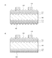
図1(A)、(B)は、本発明の一態様における光電変換装置の断面図である。該光電変
換装置は、単結晶シリコン基板100の一方の面上に第1のシリコン半導体層111、第
2のシリコン半導体層112、透光性導電膜160、第1の電極170が順に積層され、
単結晶シリコン基板100の他方の面上には、第3のシリコン半導体層113、第4のシ
リコン半導体層114、第2の電極190が順に積層された構成を有している。なお、第
1の電極170はグリッド電極であり、第1の電極170が形成された面側が受光面とな
る。また、第2の電極190もグリッド電極とし、両面を受光面とする構成としても良い
。その場合は、第4のシリコン半導体層114と第2の電極190との間に、透光性導電
膜を設けることが好ましい。
1A and 1B are cross-sectional views of a photoelectric conversion device according to one embodiment of the present invention. In the photoelectric conversion device, a first
On the other surface of the single
図1(A)は、単結晶シリコン基板100の両面に周期及び高さが数十μm以下の凹凸を
形成した構造であり、凹凸を形成するエッチング加工時にマスクを用いず、単結晶シリコ
ンの両面をエッチング加工することにより、該構造を形成することができる。また、図1
(B)は、単結晶シリコン基板100の片面のみに凹凸を形成した構造であり、凹凸を形
成するエッチング加工時に、単結晶シリコン基板の他方の面をマスクで覆うことによって
、単結晶シリコン基板の一方の面のみをエッチング加工することにより、該構造を形成す
ることができる。なお、図示はしないが、単結晶シリコン基板100の表面に上記の凹凸
を設けない構造としても良い。
FIG. 1A shows a structure in which unevenness with a period and height of several tens of μm or less is formed on both surfaces of a single
(B) is a structure in which unevenness is formed only on one surface of the single
凹凸加工された面では入射光が多重反射し、単結晶シリコン基板内には光が斜めに進行す
ることから光路長が増大する。また、裏面反射光が表面で全反射する、所謂光閉じ込め効
果を起こさせることもできる。
The incident light undergoes multiple reflections on the uneven surface, and the light travels diagonally within the single crystal silicon substrate, increasing the optical path length. In addition, a so-called light confinement effect in which the back surface reflected light is totally reflected on the front surface can be caused.
本発明の一態様において、単結晶シリコン基板100にはn型の単結晶シリコン基板を用
いることが好ましい。極力不純物を低減した単結晶シリコン基板においても少なからず不
純物が含まれており、該不純物が形成する準位にキャリアは捕獲される。該不純物の濃度
が十分に小さく、かつ同程度であるp型単結晶シリコン基板及びn型単結晶シリコン基板
の比較においては、電子捕獲断面積が、正孔捕獲断面積より大きいため、正孔が少数キャ
リアとなるn型シリコン基板の方がライフタイムが大きくなる。
In one embodiment of the present invention, the single
しかしながら、一般的な単結晶シリコン基板では、電子を少数キャリアとするp型単結晶
シリコン基板の方が拡散長は長い。そのため、n型単結晶シリコン基板を用いる場合には
、拡散長に従って基板厚を薄くしなければならない。基板厚を薄くすると光の利用効率が
低下するため、短絡電流密度が低下してしまう問題がある。
However, in a general single crystal silicon substrate, a p-type single crystal silicon substrate using electrons as minority carriers has a longer diffusion length. Therefore, when an n-type single crystal silicon substrate is used, the substrate thickness must be reduced according to the diffusion length. When the substrate thickness is reduced, the light utilization efficiency is lowered, and there is a problem that the short-circuit current density is lowered.
基板厚を薄くせずにn型単結晶シリコン基板の拡散長を高めるには、不純物及び欠陥を低
減することが必要となる。本発明の一態様においては、低酸素濃度のn型単結晶シリコン
基板を用いる。例えば、酸素濃度が8×10¹⁷atoms/cm3以下、好ましくは5
×1017atoms/cm3以下、更に好ましくは3×1017atoms/cm3以
下のn型単結晶シリコン基板を用いる。ここで、単結晶シリコン中の酸素とは、格子間酸
素を指す。このような低酸素濃度のシリコンウェハは、FZ(Floating Zon
e)法や、MCZ(Magnetic field applied Czochral
ski)法などで作製することができる。また、上記酸素濃度は、フーリエ変換赤外分光
法(換算係数4.81×10¹⁷/cm2)で求めることができる。
In order to increase the diffusion length of the n-type single crystal silicon substrate without reducing the substrate thickness, it is necessary to reduce impurities and defects. In one embodiment of the present invention, a low oxygen concentration n-type single crystal silicon substrate is used. For example, the oxygen concentration is 8 × 10 17 atoms / cm 3 or less, preferably 5
An n-type single crystal silicon substrate of × 10 17 atoms / cm 3 or less, more preferably 3 × 10 17 atoms / cm 3 or less is used. Here, oxygen in single crystal silicon refers to interstitial oxygen. Such a low oxygen concentration silicon wafer is FZ (Floating Zon).
e) Method and MCZ (Magnetic field applied Czochral)
ski) method or the like. The oxygen concentration can be determined by Fourier transform infrared spectroscopy (conversion factor: 4.81 × 10 17 / cm 2 ).
第1のシリコン半導体層111及び第3のシリコン半導体層113は、欠陥が少ない高品
質なi型半導体層であり、単結晶シリコン基板100の表面欠陥を低減することができる
。なお、本明細書において、i型の半導体とは、フェルミ準位がバンドギャップの中央に
位置する所謂真性半導体の他、半導体に含まれるp型を付与する不純物およびn型を付与
する不純物が1×10²⁰atoms/cm3以下の濃度であり、暗伝導度に対して光伝
導度が高い半導体を指す。
The first
例えば、第1のシリコン半導体層111、第3のシリコン半導体層113には、プラズマ
CVD法等で形成される非晶質シリコンまたは微結晶シリコンを用いることができる。ま
たは、該シリコン半導体層に相当する領域が、結晶シリコン領域及び非晶質シリコン領域
を含む領域であっても良い。
For example, the first
上記結晶シリコン領域は、単結晶シリコン基板100と接する領域においては、該単結晶
シリコン基板の原子配列を受け継いだ、結晶成長領域である。したがって、該単結晶シリ
コン基板と該結晶シリコン領域との間には、明瞭な界面は形成されず、両者は実質的に一
体となっている。すなわち、該結晶シリコン領域は、該単結晶シリコン基板と同程度の良
好な結晶品質を有し、極めて不純物や欠陥の少ない領域であるといえる。
In the region in contact with the single
また、上記結晶シリコン領域上には、非晶質シリコン領域が形成されている。該非晶質シ
リコン領域は、該結晶シリコン領域と連続形成された領域である。例えば、該結晶シリコ
ン領域及び該非晶質シリコン領域は、プラズマCVD法などを用いて該結晶シリコン領域
を形成した後に、洗浄や搬送などを含む他の工程を一切介さずに該非晶質シリコン領域を
形成する。または、該結晶シリコン領域の形成プロセス終了前に該非晶質シリコン領域の
形成プロセスを開始することにより形成する。
An amorphous silicon region is formed on the crystalline silicon region. The amorphous silicon region is a region formed continuously with the crystalline silicon region. For example, after the crystalline silicon region and the amorphous silicon region are formed by using a plasma CVD method or the like, the amorphous silicon region is not subjected to any other process including cleaning and transportation. Form. Alternatively, the amorphous silicon region forming process is started before the crystalline silicon region forming process is completed.
このように、他の工程が行われずに連続形成された上記結晶シリコン領域と上記非晶質シ
リコン領域の間には、不純物濃度の高い領域や酸化層などが生成されることなく、明瞭な
界面が形成されない。したがって、両者は実質的に連続した構造、または連続的に変化す
る構造を有しているということができる。
As described above, a clear interface is not formed between the crystalline silicon region and the amorphous silicon region, which are continuously formed without performing other steps, without generating a region with high impurity concentration or an oxide layer. Is not formed. Therefore, it can be said that both have a substantially continuous structure or a continuously changing structure.
なお、上記結晶シリコン領域及び上記非晶質シリコン領域を含む領域においては、該結晶
シリコン領域が占める割合が高いほど好ましい。しかしながら、結晶シリコンの表面は未
結合手などの欠陥が多いため、少なくとも該結晶シリコン領域の表面が露出することがな
いように水素を含む非晶質シリコン領域で該結晶シリコン領域の表面を覆い、該欠陥を水
素で終端する構成とすることが好ましい。
Note that in a region including the crystalline silicon region and the amorphous silicon region, it is preferable that the proportion occupied by the crystalline silicon region is higher. However, since the surface of the crystalline silicon has many defects such as dangling bonds, at least the surface of the crystalline silicon region is covered with an amorphous silicon region containing hydrogen so that the surface of the crystalline silicon region is not exposed, The defect is preferably terminated with hydrogen.
上記の説明の通り、単結晶シリコン基板100と上記結晶シリコン領域、及び上記結晶シ
リコン領域と上記非晶質シリコン領域との間には明瞭な界面が形成されないため、界面に
存在する欠陥や不純物により形成される局在準位の影響を排除することができる。また、
該結晶シリコン領域は欠陥が少なく、該結晶シリコン領域及び該非晶質シリコン領域を含
む領域全体における欠陥の絶対量を少なくすることができるため、キャリアの再結合を低
減させることができる。
As described above, a clear interface is not formed between the single
Since the crystalline silicon region has few defects and the absolute amount of defects in the entire region including the crystalline silicon region and the amorphous silicon region can be reduced, carrier recombination can be reduced.
また、上記結晶シリコン領域の表面は、高さ及び周期がナノメートルサイズの凹凸形状を
しており、この形状も前述した凹凸の光学的作用と同等の作用を有する。したがって、図
1(A)、(B)に示す光電変換装置は、マイクロメートルサイズの凹凸の表面にナノメ
ートルサイズの凹凸を有する構造とすることができるため、光学的作用によって電気特性
を大きく向上させることができる。
Further, the surface of the crystalline silicon region has a concavo-convex shape with a height and a period of nanometer size, and this shape also has an effect equivalent to the optical action of the concavo-convex described above. Therefore, the photoelectric conversion device illustrated in FIGS. 1A and 1B can have a structure having nanometer-size unevenness on the surface of micrometer-size unevenness, and thus greatly improves electrical characteristics by optical action. Can be made.
また、本発明の一態様では、第1のシリコン半導体層111及び第3のシリコン半導体層
113に含まれる不純物元素を極力低減させることが好ましい。プラズマCVD法等で形
成されるシリコン半導体層などには、原料ガスが高純度であっても成膜チャンバー中に残
留する大気成分やクリーニングガス成分が不純物として膜中に取り込まれやすい。これら
の不純物はエネルギーギャップ中に不純物準位を形成し、キャリアの捕獲などの悪影響を
与える。
In one embodiment of the present invention, it is preferable to reduce impurity elements contained in the first
発明者らの実験結果では、窒素、酸素などの大気成分については、膜中の濃度を1×10
17atoms/cm3以下とすることで、その影響をほとんど排除できることが判明し
ている。また、クリーニングガスの成分であるフッ素の膜中濃度は、窒素及び/または酸
素の膜中濃度以下にすることが好ましいことが判明している。
According to the results of experiments conducted by the inventors, for atmospheric components such as nitrogen and oxygen, the concentration in the film is 1 × 10.
It has been found that the influence can be almost eliminated by setting it to 17 atoms / cm 3 or less. Further, it has been found that the concentration of fluorine, which is a component of the cleaning gas, in the film is preferably less than or equal to the concentration of nitrogen and / or oxygen in the film.
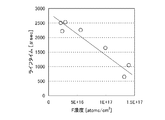
図2は、単結晶シリコン基板の両面にフッ素濃度の異なる非晶質シリコン半導体層を形成
したサンプルのライフタイム測定結果である。該単結晶シリコン基板には酸素濃度が8×
1017atoms/cm3以下のn型単結晶シリコン基板を用い、該非晶質シリコン半
導体層は、フッ素濃度が変化するように成膜条件を調整して形成している。
FIG. 2 shows a lifetime measurement result of a sample in which amorphous silicon semiconductor layers having different fluorine concentrations are formed on both surfaces of a single crystal silicon substrate. The single crystal silicon substrate has an oxygen concentration of 8 ×
An n-type single crystal silicon substrate of 10 17 atoms / cm 3 or less is used, and the amorphous silicon semiconductor layer is formed by adjusting the film formation conditions so that the fluorine concentration changes.
バルク特性が良好な単結晶シリコン基板を用いているために、フッ素濃度が高めであって
も1000μsec前後のライフタイムを示しているが、フッ素濃度を1×10¹⁷at
oms/cm3以下とすることで、ライフタイムは1500μsec以上を示すようにな
る。更にはフッ素濃度を6×10¹⁶atoms/cm3以下とすることで、ライフタイ
ムは極めて高い2000μsec以上を示すようになる。したがって、単結晶シリコン基
板の表面にパッシベーション層として形成するシリコン半導体層のフッ素濃度は、1×1
017atoms/cm3以下とすることが好ましく、6×1016atoms/cm3
以下とすることが更に好ましい。
Since a single crystal silicon substrate having good bulk characteristics is used, a lifetime of around 1000 μsec is shown even if the fluorine concentration is high, but the fluorine concentration is 1 × 10 17 at.
By setting it to oms / cm 3 or less, the lifetime becomes 1500 μsec or more. Furthermore, by setting the fluorine concentration to 6 × 10 16 atoms / cm 3 or less, the lifetime is as high as 2000 μsec or more. Therefore, the fluorine concentration of the silicon semiconductor layer formed as a passivation layer on the surface of the single crystal silicon substrate is 1 × 1.
0 17 atoms / cm 3 or less is preferable, and 6 × 10 16 atoms / cm 3 is preferable.
More preferably, it is as follows.
また、上記シリコン半導体層のフッ素濃度は、該シリコン半導体層の窒素濃度、及び酸素
濃度よりも低いことが好ましい。図3は、単結晶シリコン基板の両面にシリコン半導体層
を形成した複数のサンプルにおいて、該シリコン半導体層の窒素濃度とフッ素濃度との差
分(CN−CF)及び酸素濃度とフッ素濃度との差分(CO−CF)のぞれぞれと、該サ
ンプルのライフタイムを比較した結果である。
The fluorine concentration of the silicon semiconductor layer is preferably lower than the nitrogen concentration and oxygen concentration of the silicon semiconductor layer. FIG. 3 shows the difference (C N −C F ) between the nitrogen concentration and the fluorine concentration of the silicon semiconductor layer and the oxygen concentration and the fluorine concentration in a plurality of samples in which silicon semiconductor layers are formed on both surfaces of the single crystal silicon substrate. This is a result of comparing the difference (C O −C F ) with the lifetime of the sample.
図3より、ライフタイムが2000μsec付近でCN−CF及びCO−CFの値の正負
が入れ替わっていることがわかる。該値が正の場合は、窒素濃度または酸素濃度よりもフ
ッ素濃度が低いことを示しており、該値が正であることは、高いライフタイムを達成する
ための明確な指標であることがわかる。
As can be seen from FIG. 3, the values of C N -C F and C O -C F are interchanged when the lifetime is around 2000 μsec. When the value is positive, it indicates that the fluorine concentration is lower than the nitrogen concentration or the oxygen concentration, and it is understood that the positive value is a clear indicator for achieving a high lifetime. .
つまり、高いライフタイムを達成するためには、シリコン半導体層(パッシベーション層
)のフッ素濃度を1×10¹⁷atoms/cm3以下とするだけでなく、該フッ素濃度
をシリコン半導体層の窒素濃度及び酸素濃度のいずれか、または両方より低い値とするこ
とが好ましい。なお、シリコン半導体層のフッ素濃度が1×10¹⁷atoms/cm3
以上である場合には、窒素濃度及び酸素濃度とライフタイムとの相関は見られない。
That is, in order to achieve a high lifetime, not only the fluorine concentration of the silicon semiconductor layer (passivation layer) is 1 × 10 17 atoms / cm 3 or less, but also the fluorine concentration is reduced to the nitrogen concentration and oxygen concentration of the silicon semiconductor layer. It is preferable to set a value lower than either or both of the concentrations. Note that the fluorine concentration of the silicon semiconductor layer is 1 × 10 17 atoms / cm 3.
In the above case, there is no correlation between the nitrogen concentration and oxygen concentration and the lifetime.
上述したシリコン半導体層を第1のシリコン半導体層111及び第3のシリコン半導体層
113として単結晶シリコン基板100の表面に形成することで、該単結晶シリコン基板
のライフタイムを向上させることができ、電気特性が良好な光電変換装置を形成すること
ができる。特に、該単結晶シリコン基板の表面に凹凸を設ける場合には、その効果が顕著
となる。
By forming the above-described silicon semiconductor layers on the surface of the single
単結晶シリコン基板100は一導電型を有し、第2のシリコン半導体層112は、単結晶
シリコン基板100の導電型とは逆の導電型を有する半導体層である。単結晶シリコン基
板100がn型の場合には、第2のシリコン半導体層112はp型であり、単結晶シリコ
ン基板100と第2のシリコン半導体層112との間には、第1のシリコン半導体層11
1を介してp−n接合が形成される。
The single
A pn junction is formed through 1.
また、第4のシリコン半導体層114は、単結晶シリコン基板100と同じ導電型を有し
、該単結晶シリコン基板よりもキャリア密度の高い層である。本発明の一態様において、
単結晶シリコン基板100がn型である場合には、単結晶シリコン基板100と第4のシ
リコン半導体層114との間には、第3のシリコン半導体層113を介してn−n+接合
が形成される。つまり、第4のシリコン半導体層114は、BSF(Back Surf
ace Field)層として作用する。BSF層を形成することにより、少数キャリア
がp−n接合側にはね返されることから、第2の電極190近傍でのキャリアの再結合を
防止することができる。
The fourth
When the single
ace Field) layer. By forming the BSF layer, minority carriers rebound to the pn junction side, so that recombination of carriers in the vicinity of the
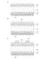
次に、図1(A)に示した光電変換装置の作製方法について図4及び図5を用いて説明す
る。
Next, a method for manufacturing the photoelectric conversion device illustrated in FIG. 1A will be described with reference to FIGS.
本実施の形態では、単結晶シリコン基板100にMCZ法で形成した酸素濃度が8×10
17atoms/cm3以下のn型単結晶シリコン基板を用いる。なお、単結晶シリコン
基板の酸素濃度が8×10¹⁷atoms/cm3以下であれば、その製法は問わない。
また、表裏に凹凸加工を行う場合は、単結晶シリコン基板の表面に(100)面を有する
基板を用いる。
In this embodiment, the oxygen concentration formed on the single
An n-type single crystal silicon substrate of 17 atoms / cm 3 or less is used. Note that there is no limitation on the manufacturing method as long as the oxygen concentration of the single crystal silicon substrate is 8 × 10 17 atoms / cm 3 or less.
In the case of performing uneven processing on the front and back, a substrate having a (100) plane on the surface of a single crystal silicon substrate is used.
次に、単結晶シリコン基板100の表裏に凹凸加工を行う。
Next, uneven processing is performed on the front and back of the single
初期の単結晶シリコン基板100がスライス加工のみである基板の場合は、単結晶シリコ
ン基板100の表面から10〜20μmに残留するダメージ層をウエットエッチング工程
にて取り除く。エッチング液には、比較的高濃度のアルカリ溶液、例えば、10〜50%
の水酸化ナトリウム水溶液、または同濃度の水酸化カリウム水溶液を用いることができる
。または、フッ酸と硝酸を混合した混酸や、それらに酢酸を混合した混酸を用いても良い
。
In the case where the initial single
An aqueous solution of sodium hydroxide or an aqueous solution of potassium hydroxide having the same concentration can be used. Alternatively, a mixed acid in which hydrofluoric acid and nitric acid are mixed, or a mixed acid in which acetic acid is mixed with them may be used.
次に、ダメージ層除去後の単結晶シリコン基板表面に付着している不純物を酸洗浄で取り
除く。酸としては、例えば、0.5%フッ酸と1%過酸化水素水の混合液(FPM)など
を用いることができる。またはRCA洗浄などを行っても良い。なお、この酸洗浄工程は
省いても良い。
Next, the impurities adhering to the surface of the single crystal silicon substrate after removing the damaged layer are removed by acid cleaning. As the acid, for example, a mixed solution (FPM) of 0.5% hydrofluoric acid and 1% hydrogen peroxide water can be used. Alternatively, RCA cleaning or the like may be performed. This acid cleaning step may be omitted.
凹凸は、結晶シリコンのアルカリ溶液によるエッチングにおいて、面方位に対するエッチ
ングレートの違いを利用して形成する。エッチング液には比較的低濃度のアルカリ溶液、
例えば、1〜5%の水酸化ナトリウム水溶液、または同濃度の水酸化カリウム水溶液を用
いることができ、好ましくは、数%のイソプロピルアルコールを添加する。エッチング液
の温度は70〜90℃とし、30〜60分間、単結晶シリコン基板をエッチング液に浸漬
する。この処理により、単結晶シリコン基板100表面に、微細な略四角錐状の複数の凸
部、及び隣接する凸部間で構成される凹部からなる凹凸を形成することができる。
The unevenness is formed by utilizing the difference in etching rate with respect to the plane orientation in etching with an alkaline solution of crystalline silicon. The etching solution contains a relatively low concentration alkaline solution,
For example, a 1 to 5% aqueous sodium hydroxide solution or an aqueous potassium hydroxide solution having the same concentration can be used, and preferably several percent of isopropyl alcohol is added. The temperature of the etching solution is 70 to 90 ° C., and the single crystal silicon substrate is immersed in the etching solution for 30 to 60 minutes. By this treatment, the surface of the single
次に、上述の凹凸を形成するためのエッチング工程では、単結晶シリコン基板の表層に不
均一な酸化層が形成されるため、該酸化層を取り除く。また、該酸化層にはアルカリ溶液
の成分が残存しやすいため、それを取り除く目的もある。アルカリ金属、例えばNaイオ
ンやKイオンがシリコン中に侵入するとライフタイムが劣化するため、光電変換装置の電
気特性が著しく低下してしまう。なお、この酸化層を除去するには、1〜5%の希フッ酸
を用いれば良い。
Next, in the etching process for forming the unevenness described above, a non-uniform oxide layer is formed on the surface layer of the single crystal silicon substrate, and thus the oxide layer is removed. Moreover, since the components of the alkaline solution are likely to remain in the oxide layer, there is also an object to remove them. When an alkali metal such as Na ion or K ion enters silicon, the lifetime is deteriorated, so that the electrical characteristics of the photoelectric conversion device are remarkably deteriorated. In order to remove the oxide layer, 1 to 5% dilute hydrofluoric acid may be used.
次に、フッ酸と硝酸を混合した混酸、または、それらに酢酸を混合した混酸を用いて単結
晶シリコン基板100の表面をエッチングし、金属成分などの不純物を除去することが好
ましい。酢酸を混合することで、硝酸の酸化力を維持し、エッチング工程を安定にする効
果、及びエッチングレートを調整する効果が得られる。例えば、各酸の体積比率は、フッ
酸:硝酸:酢酸=1:(1.5〜3):(2〜4)とすることができる。なお、本明細書
では、フッ酸、硝酸及び酢酸の混酸液をフッ硝酢酸と呼ぶ。また、このフッ硝酢酸を用い
たエッチング工程では、凸部の頂点の断面における角度を大きくする方向に変化させるこ
とから、表面積が低減し、表面欠陥の絶対量を低減することができる。なお、このフッ硝
酢酸を用いたエッチングを行う場合は、上述の希フッ酸を用いた酸化層の除去工程を省く
こともできる。ここまでの工程により、図4(A)に示す単結晶シリコン基板の断面形状
が形成される。
Next, it is preferable to remove impurities such as metal components by etching the surface of the single
次いで、適切な洗浄の後、単結晶シリコン基板100の一面にプラズマCVD法を用いて
第3のシリコン半導体層113を形成する。本実施の形態において、第3のシリコン半導
体層113は、i型の非晶質シリコン半導体層とし、膜厚は3nm以上50nm以下とす
ることが好ましい。
Next, after appropriate cleaning, a third
第3のシリコン半導体層113は、例えば、反応室にモノシランを導入し、反応室内の圧
力を100Pa以上200Pa以下、電極間隔を10mm以上40mm以下、カソード電
極の面積を基準とする電力密度を8mW/cm2以上120mW/cm2以下、基板温度
を150℃以上300℃以下とする条件で形成することができる。
In the third
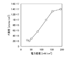
なお、図6に示すように、シリコン半導体層のフッ素濃度は、成膜時の電力密度に強く依
存する。したがって、フッ素濃度を低減させるには、電力密度を120mW/cm2以下
、好ましくは80mW/cm2以下、更に好ましくは50mW/cm2以下とする。例え
ば、反応室内の圧力を150Pa、電極間隔を10mm、電力密度を40mW/cm2、
基板温度を250℃とすれば良い。
As shown in FIG. 6, the fluorine concentration of the silicon semiconductor layer strongly depends on the power density during film formation. Therefore, in order to reduce the fluorine concentration, the power density 120 mW / cm 2 or less, preferably 80 mW / cm 2 or less, further preferably 50 mW / cm 2 or less. For example, the pressure in the reaction chamber is 150 Pa, the electrode interval is 10 mm, the power density is 40 mW / cm 2 ,
The substrate temperature may be 250 ° C.
次いで、第3のシリコン半導体層113上に第4のシリコン半導体層114を形成する(
図4(B)参照)。第4のシリコン半導体層114の厚さは3nm以上50nm以下とす
ることが好ましい。本実施の形態において、第4のシリコン半導体層114はn型の非晶
質シリコンであり、膜厚は10nmとする。
Next, a fourth
(See FIG. 4B). The thickness of the fourth
第4のシリコン半導体層114は、反応室にモノシラン及び水素ベースのホスフィン(0
.5%)を1:(1〜50)の流量比率で導入し、反応室内の圧力を100Pa以上20
0Pa以下とし、電極間隔を10mm以上40mm以下とし、カソード電極の面積を基準
とする電力密度を8mW/cm2以上120mW/cm2以下、基板温度を150℃以上
300℃以下とする条件で形成することができる。
The fourth
. 5%) is introduced at a flow rate ratio of 1: (1-50), and the pressure in the reaction chamber is increased to 100 Pa or more and 20
And 0Pa less, the electrode interval is 10mm or more 40mm or less, the power density relative to the area of the
次いで、単結晶シリコン基板100の逆の一面に、プラズマCVD法を用いて第1のシリ
コン半導体層111を形成する。第1のシリコン半導体層111の厚さは、3nm以上5
0nm以下とすることが好ましく、本実施の形態においては5nmとする。第1のシリコ
ン半導体層111は、第3のシリコン半導体層113と同様の条件にて形成することがで
きる。
Next, a first
It is preferably 0 nm or less, and in this embodiment, it is 5 nm. The first
次いで、第1のシリコン半導体層111上に第2のシリコン半導体層112を形成する(
図4(C)参照)。第2のシリコン半導体層112の厚さは3nm以上50nm以下とす
ることが好ましい。本実施の形態において、第2のシリコン半導体層112はp型の非晶
質シリコンであり、膜厚は10nmとする。
Next, a second
(See FIG. 4C). The thickness of the second
第2のシリコン半導体層112は、反応室にモノシラン及び水素ベースのジボラン(0.
1%)を1:(2〜50)の流量比率で導入し、反応室内の圧力を100Pa以上200
Pa以下とし、電極間隔を8mm以上40mm以下とし、カソード電極の面積を基準とす
る電力密度を8mW/cm2以上50mW/cm2以下、基板温度を150℃以上300
℃以下とする条件で形成することができる。
The second
1%) is introduced at a flow rate ratio of 1: (2 to 50), and the pressure in the reaction chamber is increased to 100 Pa or more and 200
And Pa or less, the electrode interval is less than 8mm 40mm or less, the power density relative to the area of the
It can be formed under the condition of ℃ or less.
なお、本実施の形態において、上記シリコン半導体層の形成に用いる電源には、原料ガス
の分解効率の良い周波数60MHzのRF電源を用いることが好ましい。原料ガスの分解
効率を上げることで、第1のシリコン半導体層111および第3のシリコン半導体層11
3の形成時に単結晶シリコン基板100表面の未結合手を水素で終端しやすくなる。ただ
し、13.56MHz、27.12MHz、または100MHzのRF電源を用いても良
い。また、連続放電だけでなく、パルス放電にて形成を行っても良い。ON/OFF制御
、またはHigh/Low制御のパルス放電を行うことで、膜質の向上や気相中で発生す
るパーティクルを低減することができる。
Note that in this embodiment mode, it is preferable to use an RF power source with a frequency of 60 MHz with high source gas decomposition efficiency as a power source used for forming the silicon semiconductor layer. By increasing the decomposition efficiency of the source gas, the first
3, dangling bonds on the surface of the single
次いで、第4のシリコン半導体層114上に第2の電極190を形成する(図5(A)参
照)。第2の電極190には、銀、アルミニウム、銅などの低抵抗金属を用いることがで
き、スパッタ法や真空蒸着法などで形成することができる。または、スクリーン印刷法を
用いて、銀ペーストや、銅ペーストなどの導電性樹脂で形成しても良い。
Next, the
次いで、第2のシリコン半導体層112上に透光性導電膜160をスパッタ法で形成する
(図5(B)参照)。透光性導電膜160には、例えば、インジウム錫酸化物、珪素を含
むインジウム錫酸化物、亜鉛を含む酸化インジウム、酸化亜鉛、ガリウムを含む酸化亜鉛
、アルミニウムを含む酸化亜鉛、酸化錫、フッ素を含む酸化錫、アンチモンを含む酸化錫
、またはグラフェン等を用いることができる。また、透光性導電膜160は単層に限らず
、異なる膜の積層でも良い。例えば、インジウム錫酸化物とアルミニウムを含む酸化亜鉛
の積層や、インジウム錫酸化物とフッ素を含む酸化錫の積層などを用いることができる。
膜厚は総厚で10nm以上1000nm以下とする。
Next, a light-transmitting
The total thickness is 10 nm or more and 1000 nm or less.
なお、単結晶シリコン基板100の表裏に設ける膜の形成順序は、上記の方法に限らず、
図5(B)に示した構造が形成できればよい。例えば、第1のシリコン半導体層111を
形成し、その次に第3のシリコン半導体層113を形成しても良い。
Note that the order of forming the films provided on the front and back surfaces of the single
It is sufficient that the structure shown in FIG. 5B can be formed. For example, the first
次いで、スクリーン印刷法を用いて、透光性導電膜160上に導電性樹脂を供給し、焼成
して第1の電極170を形成する。ここで用いる導電性樹脂には、銀ペースト、銅ペース
ト、ニッケルペースト、モリブデンペーストなどを用いることができる。また、第1の電
極170は、銀ペーストと銅ペーストを積層するなど、異なる材料の積層であっても良い
。
Next, using a screen printing method, a conductive resin is supplied over the light-transmitting
以上により、本発明の一態様によって電気特性の優れた光電変換装置を形成することがで
きる。
As described above, according to one embodiment of the present invention, a photoelectric conversion device with excellent electric characteristics can be formed.
本実施例では、光電変換装置のセル特性について説明する。 In this embodiment, cell characteristics of a photoelectric conversion device will be described.
本実施例で説明する光電変換装置は、図1(A)に示す構造であり、MCZ法を用いて作
製した酸素濃度が8×10¹⁷atoms/cm3以下のn型単結晶シリコン基板を用い
て、実施の形態で説明した方法を用いて作製した。セルサイズは0.7cm2であり、測
定には、ソーラーシミュレータにより発生させた疑似太陽光(AM1.5、照射強度は1
00mW/cm2)を用いた。
The photoelectric conversion device described in this embodiment has a structure illustrated in FIG. 1A and uses an n-type single crystal silicon substrate having an oxygen concentration of 8 × 10 17 atoms / cm 3 or less manufactured by using the MCZ method. Then, it was manufactured using the method described in the embodiment. The cell size is 0.7 cm 2 , and the measurement is simulated sunlight generated by a solar simulator (AM1.5, irradiation intensity is 1
00 mW / cm 2 ) was used.
図7は、単結晶シリコン基板の両面に非晶質シリコン層及び接合層を設けた図4(C)の
構造で測定したライフタイムと、同サンプルに透光性導電膜及び電極を形成して図5(C
)の構造とし、I−V測定から算出した開放電圧(Voc)との関係を示す図である。な
お、ライフタイムの異なるサンプルは、該非晶質シリコン層の成膜時の電力密度を変化さ
せることにより形成した。
FIG. 7 shows a lifetime measured with the structure of FIG. 4C in which an amorphous silicon layer and a bonding layer are provided on both surfaces of a single crystal silicon substrate, and a light-transmitting conductive film and electrodes are formed on the same sample. FIG.
It is a figure which shows the relationship with the open circuit voltage (Voc) calculated from the IV measurement. Note that samples having different lifetimes were formed by changing the power density when the amorphous silicon layer was formed.
図7に示されている通り、開放電圧とライフタイムは強い相関があり、特にライフタイム
を1500μsec以上にすることが有効であることが確かめられた。したがって、本発
明の一態様は、光電変換装置の変換効率の向上に寄与することが明かとなった。
As shown in FIG. 7, the open-circuit voltage and the lifetime have a strong correlation, and it has been confirmed that it is particularly effective to set the lifetime to 1500 μsec or more. Therefore, it has been revealed that one embodiment of the present invention contributes to improvement in conversion efficiency of a photoelectric conversion device.
本実施例は、他の実施の形態と自由に組み合わすことができる。 This embodiment can be freely combined with any of the other embodiments.
100 単結晶シリコン基板
111 第1のシリコン半導体層
112 第2のシリコン半導体層
113 第3のシリコン半導体層
114 第4のシリコン半導体層
160 透光性導電膜
170 第1の電極
190 第2の電極
100 single
Claims (3)
一導電型を有する単結晶シリコン基板と、
前記単結晶シリコン基板の一方の面に接する第1のシリコン半導体層と、
前記第1のシリコン半導体層に接し、前記単結晶シリコン基板とは逆の導電型を有する第2のシリコン半導体層と、
前記第2のシリコン半導体層に接する透光性導電膜と、
前記単結晶シリコン基板の他方の面に接する第3のシリコン半導体層と、
前記第3のシリコン半導体層に接し、前記単結晶シリコン基板と同じ導電型で、前記単結晶シリコン基板よりもキャリア密度の高い第4のシリコン半導体層と、を有し、
前記第1のシリコン半導体層及び前記第3のシリコン半導体層は、プラズマCVD法を用いて、反応室の圧力を100Pa以上200Pa以下、電力密度を8mW/cm2以上50mW/cm2以下で形成され、
前記第1のシリコン半導体層及び前記第3のシリコン半導体層に含有されるフッ素の濃度は、1×10¹⁷atoms/cm3未満であり、
前記第1のシリコン半導体層及び前記第3のシリコン半導体層に含有されるフッ素の濃度は、前記第1のシリコン半導体層及び前記第3のシリコン半導体層に含有される酸素の濃度よりも低いことを特徴とする光電変換装置の作製方法。 Between a pair of electrodes,
A single crystal silicon substrate having one conductivity type;
A first silicon semiconductor layer in contact with one surface of the single crystal silicon substrate;
A second silicon semiconductor layer in contact with the first silicon semiconductor layer and having a conductivity type opposite to that of the single crystal silicon substrate;
A translucent conductive film in contact with the second silicon semiconductor layer;
A third silicon semiconductor layer in contact with the other surface of the single crystal silicon substrate;
A fourth silicon semiconductor layer in contact with the third silicon semiconductor layer, having the same conductivity type as the single crystal silicon substrate and having a carrier density higher than that of the single crystal silicon substrate;
The first silicon semiconductor layer and the third silicon semiconductor layer using the plasma CVD method, pressure 100Pa or more 200Pa reaction chamber below, are formed a power density at 8 mW / cm 2 or more 50 mW / cm 2 or less ,
The concentration of fluorine contained in the first silicon semiconductor layer and the third silicon semiconductor layer is less than 1 × 10 17 atoms / cm 3 ;
The concentration of fluorine contained in the first silicon semiconductor layer and the third silicon semiconductor layer is lower than the concentration of oxygen contained in the first silicon semiconductor layer and the third silicon semiconductor layer. And a method for manufacturing a photoelectric conversion device.
一導電型を有する単結晶シリコン基板と、
前記単結晶シリコン基板の一方の面に接する第1のシリコン半導体層と、
前記第1のシリコン半導体層に接し、前記単結晶シリコン基板とは逆の導電型を有する第2のシリコン半導体層と、
前記第2のシリコン半導体層に接する透光性導電膜と、
前記単結晶シリコン基板の他方の面に接する第3のシリコン半導体層と、
前記第3のシリコン半導体層に接し、前記単結晶シリコン基板と同じ導電型で、前記単結晶シリコン基板よりもキャリア密度の高い第4のシリコン半導体層と、を有し、
前記第1のシリコン半導体層及び前記第3のシリコン半導体層は、プラズマCVD法を用いて、反応室の圧力を100Pa以上200Pa以下、電力密度を8mW/cm2以上50mW/cm2以下で形成され、
前記第1のシリコン半導体層及び前記第3のシリコン半導体層に含有されるフッ素の濃度は、1×10¹⁷atoms/cm3未満であり、
前記第1のシリコン半導体層及び前記第3のシリコン半導体層に含有されるフッ素の濃度は、前記第1のシリコン半導体層及び前記第3のシリコン半導体層に含有される窒素の濃度よりも低いことを特徴とする光電変換装置の作製方法。 Between a pair of electrodes,
A single crystal silicon substrate having one conductivity type;
A first silicon semiconductor layer in contact with one surface of the single crystal silicon substrate;
A second silicon semiconductor layer in contact with the first silicon semiconductor layer and having a conductivity type opposite to that of the single crystal silicon substrate;
A translucent conductive film in contact with the second silicon semiconductor layer;
A third silicon semiconductor layer in contact with the other surface of the single crystal silicon substrate;
A fourth silicon semiconductor layer in contact with the third silicon semiconductor layer, having the same conductivity type as the single crystal silicon substrate and having a carrier density higher than that of the single crystal silicon substrate;
The first silicon semiconductor layer and the third silicon semiconductor layer using the plasma CVD method, pressure 100Pa or more 200Pa reaction chamber below, are formed a power density at 8 mW / cm 2 or more 50 mW / cm 2 or less ,
The concentration of fluorine contained in the first silicon semiconductor layer and the third silicon semiconductor layer is less than 1 × 10 17 atoms / cm 3 ;
The concentration of fluorine contained in the first silicon semiconductor layer and the third silicon semiconductor layer is lower than the concentration of nitrogen contained in the first silicon semiconductor layer and the third silicon semiconductor layer. And a method for manufacturing a photoelectric conversion device.
一導電型を有する単結晶シリコン基板と、
前記単結晶シリコン基板の一方の面に接する第1のシリコン半導体層と、
前記第1のシリコン半導体層に接し、前記単結晶シリコン基板とは逆の導電型を有する第2のシリコン半導体層と、
前記第2のシリコン半導体層に接する透光性導電膜と、
前記単結晶シリコン基板の他方の面に接する第3のシリコン半導体層と、
前記第3のシリコン半導体層に接し、前記単結晶シリコン基板と同じ導電型で、前記単結晶シリコン基板よりもキャリア密度の高い第4のシリコン半導体層と、を有し、
前記第1のシリコン半導体層及び前記第3のシリコン半導体層は、プラズマCVD法を用いて、反応室の圧力を100Pa以上200Pa以下、電力密度を8mW/cm2以上50mW/cm2以下で形成され、
前記第1のシリコン半導体層及び前記第3のシリコン半導体層に含有されるフッ素の濃度は、1×10¹⁷atoms/cm3未満であり、
前記第1のシリコン半導体層及び前記第3のシリコン半導体層に含有されるフッ素の濃度は、前記第1のシリコン半導体層及び前記第3のシリコン半導体層に含有される窒素の濃度よりも低く、
前記第1のシリコン半導体層及び前記第3のシリコン半導体層に含有されるフッ素の濃度は、前記第1のシリコン半導体層及び前記第3のシリコン半導体層に含有される酸素の濃度よりも低いことを特徴とする光電変換装置の作製方法。 Between a pair of electrodes,
A single crystal silicon substrate having one conductivity type;
A first silicon semiconductor layer in contact with one surface of the single crystal silicon substrate;
A second silicon semiconductor layer in contact with the first silicon semiconductor layer and having a conductivity type opposite to that of the single crystal silicon substrate;
A translucent conductive film in contact with the second silicon semiconductor layer;
A third silicon semiconductor layer in contact with the other surface of the single crystal silicon substrate;
A fourth silicon semiconductor layer in contact with the third silicon semiconductor layer, having the same conductivity type as the single crystal silicon substrate and having a carrier density higher than that of the single crystal silicon substrate;
The first silicon semiconductor layer and the third silicon semiconductor layer using the plasma CVD method, pressure 100Pa or more 200Pa reaction chamber below, are formed a power density at 8 mW / cm 2 or more 50 mW / cm 2 or less ,
The concentration of fluorine contained in the first silicon semiconductor layer and the third silicon semiconductor layer is less than 1 × 10 17 atoms / cm 3 ;
The concentration of fluorine contained in the first silicon semiconductor layer and the third silicon semiconductor layer is lower than the concentration of nitrogen contained in the first silicon semiconductor layer and the third silicon semiconductor layer,
The concentration of fluorine contained in the first silicon semiconductor layer and the third silicon semiconductor layer is lower than the concentration of oxygen contained in the first silicon semiconductor layer and the third silicon semiconductor layer. And a method for manufacturing a photoelectric conversion device.
Applications Claiming Priority (2)
| Application Number | Priority Date | Filing Date | Title |
|---|---|---|---|
| JP2011132101 | 2011-06-14 | ||
| JP2011132101 | 2011-06-14 |
Related Parent Applications (1)
| Application Number | Title | Priority Date | Filing Date |
|---|---|---|---|
| JP2012134023A Division JP2013021309A (en) | 2011-06-14 | 2012-06-13 | Photoelectric conversion device |
Publications (1)
| Publication Number | Publication Date |
|---|---|
| JP2017005270A true JP2017005270A (en) | 2017-01-05 |
Family
ID=47352991
Family Applications (2)
| Application Number | Title | Priority Date | Filing Date |
|---|---|---|---|
| JP2012134023A Withdrawn JP2013021309A (en) | 2011-06-14 | 2012-06-13 | Photoelectric conversion device |
| JP2016180242A Withdrawn JP2017005270A (en) | 2011-06-14 | 2016-09-15 | Method of manufacturing photoelectric conversion device |
Family Applications Before (1)
| Application Number | Title | Priority Date | Filing Date |
|---|---|---|---|
| JP2012134023A Withdrawn JP2013021309A (en) | 2011-06-14 | 2012-06-13 | Photoelectric conversion device |
Country Status (2)
| Country | Link |
|---|---|
| US (1) | US20120319157A1 (en) |
| JP (2) | JP2013021309A (en) |
Families Citing this family (3)
| Publication number | Priority date | Publication date | Assignee | Title |
|---|---|---|---|---|
| WO2016084299A1 (en) * | 2014-11-28 | 2016-06-02 | パナソニックIpマネジメント株式会社 | Solar cell and solar cell module |
| IT201700004876A1 (en) * | 2017-01-18 | 2018-07-18 | Enel Green Power Spa | Solar cell apparatus and relative production method for single cells, tandems and heterojunction systems |
| CN114667370A (en) | 2019-08-09 | 2022-06-24 | 尖端设备技术公司 | Producing tapes or wafers having regions of low oxygen concentration |
Citations (4)
| Publication number | Priority date | Publication date | Assignee | Title |
|---|---|---|---|---|
| JP2008235400A (en) * | 2007-03-19 | 2008-10-02 | Sanyo Electric Co Ltd | Photovoltaic device |
| WO2010005439A1 (en) * | 2008-07-09 | 2010-01-14 | Applied Materials, Inc. | Solar cells and methods and apparatuses for forming the same |
| JP2011003750A (en) * | 2009-06-19 | 2011-01-06 | Kaneka Corp | Crystal silicon system solar cell |
| WO2011062286A1 (en) * | 2009-11-20 | 2011-05-26 | 京セラ株式会社 | Deposited film forming device |
Family Cites Families (6)
| Publication number | Priority date | Publication date | Assignee | Title |
|---|---|---|---|---|
| JP3203078B2 (en) * | 1992-12-09 | 2001-08-27 | 三洋電機株式会社 | Photovoltaic element |
| US6875674B2 (en) * | 2000-07-10 | 2005-04-05 | Semiconductor Energy Laboratory Co., Ltd. | Method of manufacturing a semiconductor device with fluorine concentration |
| JP2002057351A (en) * | 2000-08-15 | 2002-02-22 | Shin Etsu Handotai Co Ltd | Solar battery and its manufacturing method |
| US6743700B2 (en) * | 2001-06-01 | 2004-06-01 | Semiconductor Energy Laboratory Co., Ltd. | Semiconductor film, semiconductor device and method of their production |
| KR101234881B1 (en) * | 2007-12-20 | 2013-02-20 | 시마 나노 테크 이스라엘 리미티드 | Photovoltaic device having transparent electrode formed with nanoparticles |
| KR101146736B1 (en) * | 2009-09-14 | 2012-05-17 | 엘지전자 주식회사 | Solar cell |
-
2012
- 2012-06-05 US US13/488,480 patent/US20120319157A1/en not_active Abandoned
- 2012-06-13 JP JP2012134023A patent/JP2013021309A/en not_active Withdrawn
-
2016
- 2016-09-15 JP JP2016180242A patent/JP2017005270A/en not_active Withdrawn
Patent Citations (4)
| Publication number | Priority date | Publication date | Assignee | Title |
|---|---|---|---|---|
| JP2008235400A (en) * | 2007-03-19 | 2008-10-02 | Sanyo Electric Co Ltd | Photovoltaic device |
| WO2010005439A1 (en) * | 2008-07-09 | 2010-01-14 | Applied Materials, Inc. | Solar cells and methods and apparatuses for forming the same |
| JP2011003750A (en) * | 2009-06-19 | 2011-01-06 | Kaneka Corp | Crystal silicon system solar cell |
| WO2011062286A1 (en) * | 2009-11-20 | 2011-05-26 | 京セラ株式会社 | Deposited film forming device |
Also Published As
| Publication number | Publication date |
|---|---|
| US20120319157A1 (en) | 2012-12-20 |
| JP2013021309A (en) | 2013-01-31 |
Similar Documents
| Publication | Publication Date | Title |
|---|---|---|
| JP5456168B2 (en) | Method for manufacturing photoelectric conversion device | |
| JP5421701B2 (en) | Crystalline silicon solar cell and manufacturing method thereof | |
| KR100971658B1 (en) | Method for texturing of silicon solar cell | |
| US20120273036A1 (en) | Photoelectric conversion device and manufacturing method thereof | |
| US9761749B2 (en) | Photoelectric conversion device | |
| JP5948148B2 (en) | Photoelectric conversion device | |
| US9508880B2 (en) | Method for processing a minute structure on a surface of the silicon substrate | |
| JP2014082285A (en) | Solar cell, method for manufacturing the same, and solar cell module | |
| JP2017005270A (en) | Method of manufacturing photoelectric conversion device | |
| TWI390755B (en) | Method of fabricating solar cells | |
| KR101474008B1 (en) | Method for preparing of solar cell using plasma-surface-treatment | |
| KR101686663B1 (en) | Thin Back Contact Solar Cells and Manufacturing Method thereof | |
| US9437768B2 (en) | Photoelectric conversion device | |
| JP5745653B2 (en) | Photovoltaic device, manufacturing method thereof, and photovoltaic module | |
| JP6139731B2 (en) | Method for manufacturing photoelectric conversion device | |
| JP5927028B2 (en) | Photoelectric conversion device | |
| WO2017010029A1 (en) | Photoelectric conversion device | |
| JP6990764B2 (en) | Solar cells and their manufacturing methods | |
| JP2013125884A (en) | Photoelectric conversion device manufacturing method and photoelectric conversion device | |
| TWI790245B (en) | Manufacturing method of photoelectric conversion device | |
| KR20130061346A (en) | Solar cell and method of manufacturing the same | |
| KR101437162B1 (en) | Method for preparing of solar cell using plasma-surface-treatment | |
| JP2014107551A (en) | Surface treatment method of substrate for solar cell | |
| KR101431266B1 (en) | Method for manufacturing solar cell | |
| JP2013074038A (en) | Method of manufacturing photoelectric conversion device and photoelectric conversion device |
Legal Events
| Date | Code | Title | Description |
|---|---|---|---|
| A977 | Report on retrieval |
Free format text: JAPANESE INTERMEDIATE CODE: A971007 Effective date: 20170621 |
|
| A131 | Notification of reasons for refusal |
Free format text: JAPANESE INTERMEDIATE CODE: A131 Effective date: 20170627 |
|
| A761 | Written withdrawal of application |
Free format text: JAPANESE INTERMEDIATE CODE: A761 Effective date: 20170822 |