JP6081719B2 - カードコネクタ - Google Patents
カードコネクタ Download PDFInfo
- Publication number
- JP6081719B2 JP6081719B2 JP2012148716A JP2012148716A JP6081719B2 JP 6081719 B2 JP6081719 B2 JP 6081719B2 JP 2012148716 A JP2012148716 A JP 2012148716A JP 2012148716 A JP2012148716 A JP 2012148716A JP 6081719 B2 JP6081719 B2 JP 6081719B2
- Authority
- JP
- Japan
- Prior art keywords
- movable terminal
- card
- contact
- terminal
- movable
- Prior art date
- Legal status (The legal status is an assumption and is not a legal conclusion. Google has not performed a legal analysis and makes no representation as to the accuracy of the status listed.)
- Expired - Fee Related
Links
Images


Classifications
-
- H—ELECTRICITY
- H01—ELECTRIC ELEMENTS
- H01R—ELECTRICALLY-CONDUCTIVE CONNECTIONS; STRUCTURAL ASSOCIATIONS OF A PLURALITY OF MUTUALLY-INSULATED ELECTRICAL CONNECTING ELEMENTS; COUPLING DEVICES; CURRENT COLLECTORS
- H01R13/00—Details of coupling devices of the kinds covered by groups H01R12/70 or H01R24/00 - H01R33/00
- H01R13/62—Means for facilitating engagement or disengagement of coupling parts or for holding them in engagement
- H01R13/629—Additional means for facilitating engagement or disengagement of coupling parts, e.g. aligning or guiding means, levers, gas pressure electrical locking indicators, manufacturing tolerances
-
- H—ELECTRICITY
- H01—ELECTRIC ELEMENTS
- H01R—ELECTRICALLY-CONDUCTIVE CONNECTIONS; STRUCTURAL ASSOCIATIONS OF A PLURALITY OF MUTUALLY-INSULATED ELECTRICAL CONNECTING ELEMENTS; COUPLING DEVICES; CURRENT COLLECTORS
- H01R13/00—Details of coupling devices of the kinds covered by groups H01R12/70 or H01R24/00 - H01R33/00
- H01R13/66—Structural association with built-in electrical component
- H01R13/665—Structural association with built-in electrical component with built-in electronic circuit
- H01R13/6683—Structural association with built-in electrical component with built-in electronic circuit with built-in sensor
-
- G—PHYSICS
- G06—COMPUTING; CALCULATING OR COUNTING
- G06K—GRAPHICAL DATA READING; PRESENTATION OF DATA; RECORD CARRIERS; HANDLING RECORD CARRIERS
- G06K7/00—Methods or arrangements for sensing record carriers, e.g. for reading patterns
- G06K7/0013—Methods or arrangements for sensing record carriers, e.g. for reading patterns by galvanic contacts, e.g. card connectors for ISO-7816 compliant smart cards or memory cards, e.g. SD card readers
- G06K7/0056—Methods or arrangements for sensing record carriers, e.g. for reading patterns by galvanic contacts, e.g. card connectors for ISO-7816 compliant smart cards or memory cards, e.g. SD card readers housing of the card connector
- G06K7/0069—Methods or arrangements for sensing record carriers, e.g. for reading patterns by galvanic contacts, e.g. card connectors for ISO-7816 compliant smart cards or memory cards, e.g. SD card readers housing of the card connector including means for detecting correct insertion of the card, e.g. end detection switches notifying that the card has been inserted completely and correctly
-
- H—ELECTRICITY
- H01—ELECTRIC ELEMENTS
- H01R—ELECTRICALLY-CONDUCTIVE CONNECTIONS; STRUCTURAL ASSOCIATIONS OF A PLURALITY OF MUTUALLY-INSULATED ELECTRICAL CONNECTING ELEMENTS; COUPLING DEVICES; CURRENT COLLECTORS
- H01R12/00—Structural associations of a plurality of mutually-insulated electrical connecting elements, specially adapted for printed circuits, e.g. printed circuit boards [PCB], flat or ribbon cables, or like generally planar structures, e.g. terminal strips, terminal blocks; Coupling devices specially adapted for printed circuits, flat or ribbon cables, or like generally planar structures; Terminals specially adapted for contact with, or insertion into, printed circuits, flat or ribbon cables, or like generally planar structures
- H01R12/70—Coupling devices
- H01R12/71—Coupling devices for rigid printing circuits or like structures
Description
従来のこの種のカードコネクタとして、例えば、図13(A),(B)に示すものが知られている(特許文献1参照)。図13は、従来例のカードコネクタを示し、(A)はカードが未挿入の状態の部分平面図、(B)はカードが挿入された状態の部分平面図である。
ここで、図13(A)に示すカードCが未挿入の状態では、可動端子120が矢印X1方向に変位しており、可動端子120のワイピング部121が第1固定端子130に接触している。この状態では、第1固定端子130がオン状態、第2固定端子140がオフ状態となる。可動端子120、第1固定端子130、及び第2固定端子140は、図示しない検出回路に接続されている。検出回路は、第1固定端子130及び第2固定端子140からの検出信号の組合せ(オン、オフ)によってカードCが未挿入であることを認知する。
ここで、ワイピング部121は、第1固定端子130から移動して第2固定端子140に接触する際に、第1固定端子130及び第2固定端子140の上面上をワイピングするようになっている。
即ち、図13(A),(B)に示すカードコネクタ100においては、ワイピング部121が第1固定端子130及び第2固定端子140の上面上をワイピングする。このため、第1固定端子130及び第2固定端子140の上面上及びワイピング部121に付着している異物を除去でき、可動端子120と、第1固定端子130及び第2固定端子140との接触を確実に行うことができる。
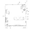
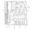
図1乃至図6に示すカードコネクタ1は、図示しない回路基板上に実装され、メモリカード、SIMカード等などのカードCが挿入及び抜去される。カードCがカードコネクタ1に挿入されることにより、カードCと回路基板との電気的接続が達成される。
カードコネクタ1は、絶縁性のハウジング10と、金属製の複数のコンタクト20と、金属製のシェル30と、カード挿入検出スイッチ機構40と、イジェクト機構70とを備えている。
更に、カード挿入検出スイッチ機構40は、カードCがハウジング10のカード挿入空間14内に挿入されたか否かを検出するものであり、図1及び図4に示すように、カードコネクタ1の後方右側部に配置される。この検出スイッチ構造40は、互いに接触可能な金属製の第1可動端子50と金属製の第2可動端子60とからなっている。
また、イジェクト機構70は、いわゆるプッシュ−プッシュ作用によるカードCの排出を可能とするもので、公知の構成を有するため、その説明は省略する。
先ず、カードCがカード挿入空間14内に挿入されると、カードCの前端角縁が第1可動端子50の当接部52に当接し、これにより、第1可動端子50が矢印Xで示す幅方向外側に変位する。そして、カードCをさらに挿入すると、図12(A)に示すように、カードCの側縁が当接部52の湾曲部52aに当接し、第1可動端子50が更に矢印Xで示す幅方向外側に変位する。これにより、第1可動端子50の当接部52が第2可動端子60の接触片部62から離間して、第1可動端子50と第2可動端子60との接触状態が解除される。このとき、第1可動端子50及び第2可動端子60が開回路を形成するから、検出回路は、カードCが挿入された状態であることを検知する。このため、カードCの挿入完了状態で、カード挿入検出スイッチ機構40を構成する第1可動端子50及び第2可動端子60が開回路を形成する。従って、カードコネクタ1が実装された機器のバッテリーの消耗を極力小さくすることができる。
また、カードCがカード挿入空間14内に挿入されるときには、図3に示すように、カードCの裏面は第2可動端子60の接触片部62に接触しない。
以上、本発明の実施形態について説明してきたが、本発明はこれに限定されずに種々の変更、改良を行うことができる。
例えば、カード挿入検出スイッチ構造40において、第1可動端子50をシェル30に設け、第2可動端子60をハウジング10に取り付ける必要は必ずしもない。
10 ハウジング
30 シェル
40 カード挿入検出スイッチ機構
50 第1可動端子
52 当接部
53 カム部
60 第2可動端子
C カード
Claims (2)
- カードが挿入及び抜去されると共に、互いに接触可能な金属製の第1可動端子及び金属製の第2可動端子からなるカード挿入検出スイッチ機構を有するカードコネクタであって、
前記第1可動端子は、前記カードの挿入時にカードが当接する当接部と、該当接部に対して傾斜するカム部とを備え、
前記カードの挿入時において、前記カードが前記当接部に当接することによって前記第1可動端子が駆動され、前記第1可動端子が前記第2可動端子から離間して前記第2可動端子との接触状態が解除され、
前記カードの抜去時において、前記カードの前記当接部に対する当接状態が解除されて前記第1可動端子が元の状態に戻り、前記カム部が前記第2可動端子に当接するとともに、前記第2可動端子は前記カム部に対してワイピングした後に前記当接部に接触するものであり、
前記第2可動端子は、前記カードの挿入時において、前記第1可動端子が駆動することにより、前記カム部に対してワイピングした後に前記第1可動端子から離間するものであり、
前記第1可動端子のカム部と前記第2可動端子との接触は、前記第1可動端子の打抜き面に前記第2可動端子の側縁が接触するものであり、
前記第1可動端子の変位の向きは、前記第2可動端子の変位の向きに対して平行な成分を有することなく前記第2可動端子の変位の向きと直交することを特徴とするカードコネクタ。 - 前記第1可動端子は前記カードが挿入されるハウジングの少なくとも一部を覆う金属製のシェルから延び、前記第2可動端子は前記ハウジングに取り付けられていることを特徴とする請求項1記載のカードコネクタ。
Priority Applications (5)
| Application Number | Priority Date | Filing Date | Title |
|---|---|---|---|
| JP2012148716A JP6081719B2 (ja) | 2012-07-02 | 2012-07-02 | カードコネクタ |
| TW102210544U TWM466395U (zh) | 2012-07-02 | 2013-06-05 | 卡連接器 |
| KR1020130076472A KR20140004027A (ko) | 2012-07-02 | 2013-07-01 | 카드 커넥터 |
| US13/933,827 US9039440B2 (en) | 2012-07-02 | 2013-07-02 | Card connector |
| CN201310273808.2A CN103531970B (zh) | 2012-07-02 | 2013-07-02 | 卡连接器 |
Applications Claiming Priority (1)
| Application Number | Priority Date | Filing Date | Title |
|---|---|---|---|
| JP2012148716A JP6081719B2 (ja) | 2012-07-02 | 2012-07-02 | カードコネクタ |
Publications (3)
| Publication Number | Publication Date |
|---|---|
| JP2014010766A JP2014010766A (ja) | 2014-01-20 |
| JP2014010766A5 JP2014010766A5 (ja) | 2015-07-09 |
| JP6081719B2 true JP6081719B2 (ja) | 2017-02-15 |
Family
ID=49778577
Family Applications (1)
| Application Number | Title | Priority Date | Filing Date |
|---|---|---|---|
| JP2012148716A Expired - Fee Related JP6081719B2 (ja) | 2012-07-02 | 2012-07-02 | カードコネクタ |
Country Status (5)
| Country | Link |
|---|---|
| US (1) | US9039440B2 (ja) |
| JP (1) | JP6081719B2 (ja) |
| KR (1) | KR20140004027A (ja) |
| CN (1) | CN103531970B (ja) |
| TW (1) | TWM466395U (ja) |
Families Citing this family (7)
| Publication number | Priority date | Publication date | Assignee | Title |
|---|---|---|---|---|
| JP1553879S (ja) * | 2015-11-03 | 2016-07-11 | ||
| JP1553611S (ja) * | 2015-11-03 | 2016-07-11 | ||
| JP1552812S (ja) * | 2015-11-03 | 2016-06-27 | ||
| JP1552814S (ja) * | 2015-11-04 | 2016-06-27 | ||
| JP1552813S (ja) * | 2015-11-04 | 2016-06-27 | ||
| JP1552815S (ja) * | 2015-11-06 | 2016-06-27 | ||
| DE102016117760A1 (de) | 2016-09-21 | 2018-03-22 | Andre HERZOG | Anordnung für einen Bewegungssimulator in Kombination mit einem stationären Ganzkörperexoskelett, einem Head-Mounted-Display und einem virtuellen Raum |
Family Cites Families (14)
| Publication number | Priority date | Publication date | Assignee | Title |
|---|---|---|---|---|
| DE4212150A1 (de) * | 1991-11-12 | 1993-05-13 | Amphenol Tuchel Elect | Chipkartenlesegeraet mit einem endlagenschalter |
| JP2000048915A (ja) * | 1998-07-30 | 2000-02-18 | Alps Electric Co Ltd | カード用コネクタ |
| JP3377477B2 (ja) * | 1999-11-08 | 2003-02-17 | 山一電機株式会社 | カードコネクタ |
| JP3635398B2 (ja) * | 2000-12-07 | 2005-04-06 | 日本航空電子工業株式会社 | 異方向変位スイッチ構造 |
| JP3718797B2 (ja) * | 2001-02-23 | 2005-11-24 | 日本航空電子工業株式会社 | カード用コネクタ |
| US6899557B2 (en) | 2001-04-23 | 2005-05-31 | Molex Incorporated | Detection switch mounted in a card socket |
| CN2737003Y (zh) * | 2004-10-27 | 2005-10-26 | 富士康(昆山)电脑接插件有限公司 | 电连接器 |
| JP4202337B2 (ja) * | 2005-05-09 | 2008-12-24 | モレックス インコーポレーテッド | カード用コネクタ |
| JP4469805B2 (ja) * | 2006-03-06 | 2010-06-02 | ホシデン株式会社 | カードコネクタ |
| JP5286126B2 (ja) | 2009-03-24 | 2013-09-11 | 富士通コンポーネント株式会社 | カード用コネクタ |
| JP5476846B2 (ja) * | 2009-08-06 | 2014-04-23 | ミツミ電機株式会社 | コネクタ及び検出スイッチ |
| US8465308B2 (en) * | 2010-10-15 | 2013-06-18 | Appple Inc. | Connector having self-wiping contacts |
| JP5727776B2 (ja) * | 2010-12-14 | 2015-06-03 | タイコエレクトロニクスジャパン合同会社 | 検出スイッチ構造及びそれを有するコネクタ |
| JP2013093233A (ja) * | 2011-10-26 | 2013-05-16 | Yamaichi Electronics Co Ltd | カード用コネクタ |
-
2012
- 2012-07-02 JP JP2012148716A patent/JP6081719B2/ja not_active Expired - Fee Related
-
2013
- 2013-06-05 TW TW102210544U patent/TWM466395U/zh not_active IP Right Cessation
- 2013-07-01 KR KR1020130076472A patent/KR20140004027A/ko not_active Application Discontinuation
- 2013-07-02 US US13/933,827 patent/US9039440B2/en not_active Expired - Fee Related
- 2013-07-02 CN CN201310273808.2A patent/CN103531970B/zh not_active Expired - Fee Related
Also Published As
| Publication number | Publication date |
|---|---|
| JP2014010766A (ja) | 2014-01-20 |
| CN103531970A (zh) | 2014-01-22 |
| US20140004735A1 (en) | 2014-01-02 |
| US9039440B2 (en) | 2015-05-26 |
| TWM466395U (zh) | 2013-11-21 |
| CN103531970B (zh) | 2018-02-23 |
| KR20140004027A (ko) | 2014-01-10 |
Similar Documents
| Publication | Publication Date | Title |
|---|---|---|
| JP6081719B2 (ja) | カードコネクタ | |
| JP5727776B2 (ja) | 検出スイッチ構造及びそれを有するコネクタ | |
| US9444196B2 (en) | Electrical connector | |
| US8070520B2 (en) | Electrical card connector | |
| US20120058657A1 (en) | Electrical card connector having detecting contacts actuated by slider | |
| JP5970391B2 (ja) | カードコネクタ | |
| JP5476846B2 (ja) | コネクタ及び検出スイッチ | |
| JP3150850U (ja) | カードコネクタ | |
| JP5400864B2 (ja) | カードコネクタ | |
| CN112909601A (zh) | 壳体组件及堆叠式卡座 | |
| JP2006114437A (ja) | カードコネクタ | |
| JP2013012451A (ja) | カード検出スイッチ付きカードコネクタ | |
| JP3897659B2 (ja) | コネクタ | |
| JP3186809U (ja) | カードコネクタ | |
| JP5410938B2 (ja) | カード用コネクタ装置 | |
| CN214254790U (zh) | 堆叠式卡座 | |
| CN215732285U (zh) | 堆叠式卡座 | |
| JP3188560U (ja) | カードコネクタ | |
| JP2016100217A (ja) | カードコネクタ | |
| KR101561195B1 (ko) | 심카드용 커넥터 | |
| KR100978511B1 (ko) | 카드용 커넥터 | |
| CN112886296A (zh) | 堆叠式卡座 | |
| KR101315675B1 (ko) | 듀얼 소켓 | |
| JP3131418U (ja) | コネクタ改良構造 | |
| KR101316847B1 (ko) | 마이크로 에스디 카드 소켓 및 그 제조방법 |
Legal Events
| Date | Code | Title | Description |
|---|---|---|---|
| A521 | Written amendment |
Free format text: JAPANESE INTERMEDIATE CODE: A523 Effective date: 20150526 |
|
| A621 | Written request for application examination |
Free format text: JAPANESE INTERMEDIATE CODE: A621 Effective date: 20150526 |
|
| A977 | Report on retrieval |
Free format text: JAPANESE INTERMEDIATE CODE: A971007 Effective date: 20160222 |
|
| A131 | Notification of reasons for refusal |
Free format text: JAPANESE INTERMEDIATE CODE: A131 Effective date: 20160308 |
|
| A521 | Written amendment |
Free format text: JAPANESE INTERMEDIATE CODE: A523 Effective date: 20160413 |
|
| A131 | Notification of reasons for refusal |
Free format text: JAPANESE INTERMEDIATE CODE: A131 Effective date: 20160726 |
|
| A521 | Written amendment |
Free format text: JAPANESE INTERMEDIATE CODE: A523 Effective date: 20160831 |
|
| A02 | Decision of refusal |
Free format text: JAPANESE INTERMEDIATE CODE: A02 Effective date: 20161004 |
|
| A521 | Written amendment |
Free format text: JAPANESE INTERMEDIATE CODE: A523 Effective date: 20161208 |
|
| A911 | Transfer to examiner for re-examination before appeal (zenchi) |
Free format text: JAPANESE INTERMEDIATE CODE: A911 Effective date: 20161219 |
|
| TRDD | Decision of grant or rejection written | ||
| A01 | Written decision to grant a patent or to grant a registration (utility model) |
Free format text: JAPANESE INTERMEDIATE CODE: A01 Effective date: 20170117 |
|
| A61 | First payment of annual fees (during grant procedure) |
Free format text: JAPANESE INTERMEDIATE CODE: A61 Effective date: 20170119 |
|
| R150 | Certificate of patent or registration of utility model |
Ref document number: 6081719 Country of ref document: JP Free format text: JAPANESE INTERMEDIATE CODE: R150 |
|
| LAPS | Cancellation because of no payment of annual fees |