JP6058876B2 - Method for depositing SiO2 film - Google Patents
Method for depositing SiO2 film Download PDFInfo
- Publication number
- JP6058876B2 JP6058876B2 JP2010286580A JP2010286580A JP6058876B2 JP 6058876 B2 JP6058876 B2 JP 6058876B2 JP 2010286580 A JP2010286580 A JP 2010286580A JP 2010286580 A JP2010286580 A JP 2010286580A JP 6058876 B2 JP6058876 B2 JP 6058876B2
- Authority
- JP
- Japan
- Prior art keywords
- teos
- film
- plasma treatment
- deposited
- frequency component
- Prior art date
- Legal status (The legal status is an assumption and is not a legal conclusion. Google has not performed a legal analysis and makes no representation as to the accuracy of the status listed.)
- Active
Links
- 238000000034 method Methods 0.000 title claims description 38
- 238000000151 deposition Methods 0.000 title claims description 32
- VYPSYNLAJGMNEJ-UHFFFAOYSA-N Silicium dioxide Chemical compound O=[Si]=O VYPSYNLAJGMNEJ-UHFFFAOYSA-N 0.000 title 2
- 229910052681 coesite Inorganic materials 0.000 title 1
- 229910052906 cristobalite Inorganic materials 0.000 title 1
- 239000000377 silicon dioxide Substances 0.000 title 1
- 235000012239 silicon dioxide Nutrition 0.000 title 1
- 229910052682 stishovite Inorganic materials 0.000 title 1
- 229910052905 tridymite Inorganic materials 0.000 title 1
- BOTDANWDWHJENH-UHFFFAOYSA-N Tetraethyl orthosilicate Chemical compound CCO[Si](OCC)(OCC)OCC BOTDANWDWHJENH-UHFFFAOYSA-N 0.000 claims description 57
- 238000009832 plasma treatment Methods 0.000 claims description 37
- 239000002243 precursor Substances 0.000 claims description 17
- 238000000623 plasma-assisted chemical vapour deposition Methods 0.000 claims description 16
- 229910004298 SiO 2 Inorganic materials 0.000 claims description 13
- 229910052710 silicon Inorganic materials 0.000 claims description 3
- 239000010703 silicon Substances 0.000 claims description 3
- 230000008021 deposition Effects 0.000 description 21
- 230000008569 process Effects 0.000 description 20
- 230000009103 reabsorption Effects 0.000 description 11
- 239000012528 membrane Substances 0.000 description 9
- 230000015556 catabolic process Effects 0.000 description 7
- 230000009102 absorption Effects 0.000 description 5
- 238000010521 absorption reaction Methods 0.000 description 5
- 238000001157 Fourier transform infrared spectrum Methods 0.000 description 4
- 230000000694 effects Effects 0.000 description 4
- 230000004044 response Effects 0.000 description 4
- 238000005033 Fourier transform infrared spectroscopy Methods 0.000 description 3
- 238000000137 annealing Methods 0.000 description 3
- 230000008859 change Effects 0.000 description 3
- 238000011282 treatment Methods 0.000 description 3
- UFHFLCQGNIYNRP-UHFFFAOYSA-N Hydrogen Chemical compound [H][H] UFHFLCQGNIYNRP-UHFFFAOYSA-N 0.000 description 2
- 229910020177 SiOF Inorganic materials 0.000 description 2
- XUIMIQQOPSSXEZ-UHFFFAOYSA-N Silicon Chemical compound [Si] XUIMIQQOPSSXEZ-UHFFFAOYSA-N 0.000 description 2
- 239000012159 carrier gas Substances 0.000 description 2
- 238000012512 characterization method Methods 0.000 description 2
- 230000007423 decrease Effects 0.000 description 2
- 238000005137 deposition process Methods 0.000 description 2
- 230000005684 electric field Effects 0.000 description 2
- 238000002474 experimental method Methods 0.000 description 2
- 239000001307 helium Substances 0.000 description 2
- 229910052734 helium Inorganic materials 0.000 description 2
- SWQJXJOGLNCZEY-UHFFFAOYSA-N helium atom Chemical compound [He] SWQJXJOGLNCZEY-UHFFFAOYSA-N 0.000 description 2
- 239000001257 hydrogen Substances 0.000 description 2
- 229910052739 hydrogen Inorganic materials 0.000 description 2
- 238000011065 in-situ storage Methods 0.000 description 2
- 238000001228 spectrum Methods 0.000 description 2
- 101000825841 Homo sapiens Vacuolar-sorting protein SNF8 Proteins 0.000 description 1
- 101100063942 Neurospora crassa (strain ATCC 24698 / 74-OR23-1A / CBS 708.71 / DSM 1257 / FGSC 987) dot-1 gene Proteins 0.000 description 1
- 102100022787 Vacuolar-sorting protein SNF8 Human genes 0.000 description 1
- FFBHFFJDDLITSX-UHFFFAOYSA-N benzyl N-[2-hydroxy-4-(3-oxomorpholin-4-yl)phenyl]carbamate Chemical compound OC1=C(NC(=O)OCC2=CC=CC=C2)C=CC(=C1)N1CCOCC1=O FFBHFFJDDLITSX-UHFFFAOYSA-N 0.000 description 1
- 230000015572 biosynthetic process Effects 0.000 description 1
- 238000006731 degradation reaction Methods 0.000 description 1
- 230000001066 destructive effect Effects 0.000 description 1
- 238000010586 diagram Methods 0.000 description 1
- 125000001301 ethoxy group Chemical group [H]C([H])([H])C([H])([H])O* 0.000 description 1
- 239000007789 gas Substances 0.000 description 1
- 238000010438 heat treatment Methods 0.000 description 1
- 230000002209 hydrophobic effect Effects 0.000 description 1
- 230000005661 hydrophobic surface Effects 0.000 description 1
- 230000006872 improvement Effects 0.000 description 1
- 238000010348 incorporation Methods 0.000 description 1
- 239000000463 material Substances 0.000 description 1
- 238000005259 measurement Methods 0.000 description 1
- 239000002184 metal Substances 0.000 description 1
- 238000002156 mixing Methods 0.000 description 1
- 239000000203 mixture Substances 0.000 description 1
- 238000002360 preparation method Methods 0.000 description 1
- 238000002203 pretreatment Methods 0.000 description 1
- 238000012545 processing Methods 0.000 description 1
- 239000012495 reaction gas Substances 0.000 description 1
- 239000000758 substrate Substances 0.000 description 1
- 238000007669 thermal treatment Methods 0.000 description 1
- 230000000007 visual effect Effects 0.000 description 1
- XLYOFNOQVPJJNP-UHFFFAOYSA-N water Chemical compound O XLYOFNOQVPJJNP-UHFFFAOYSA-N 0.000 description 1
Images


Classifications
-
- C—CHEMISTRY; METALLURGY
- C23—COATING METALLIC MATERIAL; COATING MATERIAL WITH METALLIC MATERIAL; CHEMICAL SURFACE TREATMENT; DIFFUSION TREATMENT OF METALLIC MATERIAL; COATING BY VACUUM EVAPORATION, BY SPUTTERING, BY ION IMPLANTATION OR BY CHEMICAL VAPOUR DEPOSITION, IN GENERAL; INHIBITING CORROSION OF METALLIC MATERIAL OR INCRUSTATION IN GENERAL
- C23C—COATING METALLIC MATERIAL; COATING MATERIAL WITH METALLIC MATERIAL; SURFACE TREATMENT OF METALLIC MATERIAL BY DIFFUSION INTO THE SURFACE, BY CHEMICAL CONVERSION OR SUBSTITUTION; COATING BY VACUUM EVAPORATION, BY SPUTTERING, BY ION IMPLANTATION OR BY CHEMICAL VAPOUR DEPOSITION, IN GENERAL
- C23C16/00—Chemical coating by decomposition of gaseous compounds, without leaving reaction products of surface material in the coating, i.e. chemical vapour deposition [CVD] processes
- C23C16/22—Chemical coating by decomposition of gaseous compounds, without leaving reaction products of surface material in the coating, i.e. chemical vapour deposition [CVD] processes characterised by the deposition of inorganic material, other than metallic material
- C23C16/30—Deposition of compounds, mixtures or solid solutions, e.g. borides, carbides, nitrides
- C23C16/40—Oxides
- C23C16/401—Oxides containing silicon
- C23C16/402—Silicon dioxide
-
- C—CHEMISTRY; METALLURGY
- C23—COATING METALLIC MATERIAL; COATING MATERIAL WITH METALLIC MATERIAL; CHEMICAL SURFACE TREATMENT; DIFFUSION TREATMENT OF METALLIC MATERIAL; COATING BY VACUUM EVAPORATION, BY SPUTTERING, BY ION IMPLANTATION OR BY CHEMICAL VAPOUR DEPOSITION, IN GENERAL; INHIBITING CORROSION OF METALLIC MATERIAL OR INCRUSTATION IN GENERAL
- C23C—COATING METALLIC MATERIAL; COATING MATERIAL WITH METALLIC MATERIAL; SURFACE TREATMENT OF METALLIC MATERIAL BY DIFFUSION INTO THE SURFACE, BY CHEMICAL CONVERSION OR SUBSTITUTION; COATING BY VACUUM EVAPORATION, BY SPUTTERING, BY ION IMPLANTATION OR BY CHEMICAL VAPOUR DEPOSITION, IN GENERAL
- C23C16/00—Chemical coating by decomposition of gaseous compounds, without leaving reaction products of surface material in the coating, i.e. chemical vapour deposition [CVD] processes
- C23C16/44—Chemical coating by decomposition of gaseous compounds, without leaving reaction products of surface material in the coating, i.e. chemical vapour deposition [CVD] processes characterised by the method of coating
- C23C16/455—Chemical coating by decomposition of gaseous compounds, without leaving reaction products of surface material in the coating, i.e. chemical vapour deposition [CVD] processes characterised by the method of coating characterised by the method used for introducing gases into reaction chamber or for modifying gas flows in reaction chamber
- C23C16/45563—Gas nozzles
- C23C16/45565—Shower nozzles
-
- C—CHEMISTRY; METALLURGY
- C23—COATING METALLIC MATERIAL; COATING MATERIAL WITH METALLIC MATERIAL; CHEMICAL SURFACE TREATMENT; DIFFUSION TREATMENT OF METALLIC MATERIAL; COATING BY VACUUM EVAPORATION, BY SPUTTERING, BY ION IMPLANTATION OR BY CHEMICAL VAPOUR DEPOSITION, IN GENERAL; INHIBITING CORROSION OF METALLIC MATERIAL OR INCRUSTATION IN GENERAL
- C23C—COATING METALLIC MATERIAL; COATING MATERIAL WITH METALLIC MATERIAL; SURFACE TREATMENT OF METALLIC MATERIAL BY DIFFUSION INTO THE SURFACE, BY CHEMICAL CONVERSION OR SUBSTITUTION; COATING BY VACUUM EVAPORATION, BY SPUTTERING, BY ION IMPLANTATION OR BY CHEMICAL VAPOUR DEPOSITION, IN GENERAL
- C23C16/00—Chemical coating by decomposition of gaseous compounds, without leaving reaction products of surface material in the coating, i.e. chemical vapour deposition [CVD] processes
- C23C16/44—Chemical coating by decomposition of gaseous compounds, without leaving reaction products of surface material in the coating, i.e. chemical vapour deposition [CVD] processes characterised by the method of coating
- C23C16/50—Chemical coating by decomposition of gaseous compounds, without leaving reaction products of surface material in the coating, i.e. chemical vapour deposition [CVD] processes characterised by the method of coating using electric discharges
- C23C16/505—Chemical coating by decomposition of gaseous compounds, without leaving reaction products of surface material in the coating, i.e. chemical vapour deposition [CVD] processes characterised by the method of coating using electric discharges using radio frequency discharges
-
- C—CHEMISTRY; METALLURGY
- C23—COATING METALLIC MATERIAL; COATING MATERIAL WITH METALLIC MATERIAL; CHEMICAL SURFACE TREATMENT; DIFFUSION TREATMENT OF METALLIC MATERIAL; COATING BY VACUUM EVAPORATION, BY SPUTTERING, BY ION IMPLANTATION OR BY CHEMICAL VAPOUR DEPOSITION, IN GENERAL; INHIBITING CORROSION OF METALLIC MATERIAL OR INCRUSTATION IN GENERAL
- C23C—COATING METALLIC MATERIAL; COATING MATERIAL WITH METALLIC MATERIAL; SURFACE TREATMENT OF METALLIC MATERIAL BY DIFFUSION INTO THE SURFACE, BY CHEMICAL CONVERSION OR SUBSTITUTION; COATING BY VACUUM EVAPORATION, BY SPUTTERING, BY ION IMPLANTATION OR BY CHEMICAL VAPOUR DEPOSITION, IN GENERAL
- C23C16/00—Chemical coating by decomposition of gaseous compounds, without leaving reaction products of surface material in the coating, i.e. chemical vapour deposition [CVD] processes
- C23C16/44—Chemical coating by decomposition of gaseous compounds, without leaving reaction products of surface material in the coating, i.e. chemical vapour deposition [CVD] processes characterised by the method of coating
- C23C16/52—Controlling or regulating the coating process
-
- C—CHEMISTRY; METALLURGY
- C23—COATING METALLIC MATERIAL; COATING MATERIAL WITH METALLIC MATERIAL; CHEMICAL SURFACE TREATMENT; DIFFUSION TREATMENT OF METALLIC MATERIAL; COATING BY VACUUM EVAPORATION, BY SPUTTERING, BY ION IMPLANTATION OR BY CHEMICAL VAPOUR DEPOSITION, IN GENERAL; INHIBITING CORROSION OF METALLIC MATERIAL OR INCRUSTATION IN GENERAL
- C23C—COATING METALLIC MATERIAL; COATING MATERIAL WITH METALLIC MATERIAL; SURFACE TREATMENT OF METALLIC MATERIAL BY DIFFUSION INTO THE SURFACE, BY CHEMICAL CONVERSION OR SUBSTITUTION; COATING BY VACUUM EVAPORATION, BY SPUTTERING, BY ION IMPLANTATION OR BY CHEMICAL VAPOUR DEPOSITION, IN GENERAL
- C23C16/00—Chemical coating by decomposition of gaseous compounds, without leaving reaction products of surface material in the coating, i.e. chemical vapour deposition [CVD] processes
- C23C16/56—After-treatment
-
- H—ELECTRICITY
- H01—ELECTRIC ELEMENTS
- H01L—SEMICONDUCTOR DEVICES NOT COVERED BY CLASS H10
- H01L21/00—Processes or apparatus adapted for the manufacture or treatment of semiconductor or solid state devices or of parts thereof
- H01L21/02—Manufacture or treatment of semiconductor devices or of parts thereof
- H01L21/02104—Forming layers
- H01L21/02365—Forming inorganic semiconducting materials on a substrate
- H01L21/02612—Formation types
- H01L21/02617—Deposition types
- H01L21/0262—Reduction or decomposition of gaseous compounds, e.g. CVD
-
- H—ELECTRICITY
- H01—ELECTRIC ELEMENTS
- H01L—SEMICONDUCTOR DEVICES NOT COVERED BY CLASS H10
- H01L21/00—Processes or apparatus adapted for the manufacture or treatment of semiconductor or solid state devices or of parts thereof
- H01L21/67—Apparatus specially adapted for handling semiconductor or electric solid state devices during manufacture or treatment thereof; Apparatus specially adapted for handling wafers during manufacture or treatment of semiconductor or electric solid state devices or components ; Apparatus not specifically provided for elsewhere
- H01L21/67005—Apparatus not specifically provided for elsewhere
- H01L21/67011—Apparatus for manufacture or treatment
- H01L21/67155—Apparatus for manufacturing or treating in a plurality of work-stations
- H01L21/67207—Apparatus for manufacturing or treating in a plurality of work-stations comprising a chamber adapted to a particular process
Description
本発明は、SiO2膜を堆積する方法に関し、特に、そのような膜を、プラズマ化学気相成長法(PECVD)を用いて250℃より下の温度で堆積することに関する。 The present invention relates to a method of depositing a SiO 2 film, and in particular to depositing such a film at a temperature below 250 ° C. using plasma enhanced chemical vapor deposition (PECVD).
例えばシリコン中のエッチングされたビア又はトレンチとすることができるシリコン貫通電極(TVS)は、金属層を堆積する前に誘電性ライナ(dielectric liner)を必要とする。そのような膜が良好なコンフォーマル(conformal)膜であることは、通常の使用におけるリーク電流を回避するために誘電特性を十分良好にする必要がある厚さが最小となるために非常に望ましい。非常に一般的には次のステップで真空破壊を伴う堆積ステップに伴う吸湿を制限する必要もある。コンフォーマルかつ吸水のない状態で膜を低温、好適には200℃より下の温度で堆積できることも望まれている。 For example, through silicon vias (TVS), which can be etched vias or trenches in silicon, require a dielectric liner before depositing the metal layer. It is highly desirable that such a film be a good conformal film, as it minimizes the thickness that needs to have good dielectric properties to avoid leakage currents in normal use. . Very generally, it is also necessary to limit the moisture absorption associated with the deposition step with a vacuum break in the next step. It would also be desirable to be able to deposit films at low temperatures, preferably below 200 ° C. in a conformal and water-absorbing state.
TEOS/O2前駆体を用いたPECVDが考えられてきた。その理由は、TEOS/O2前駆体が一般的に良好なステップカバレージを有するとともに前駆体のコストが比較的低いからである。しかしながら、堆積温度を200℃−250℃より下に低減したとき、誘電特性(リーク及び最終的な破壊)が劣化し始める。Kim等によるTEOS2前駆体及びTEOS/O2/CF4前駆体からのRF PECVD技術を用いたSiO2膜及びSiOF膜の特性評価及び生成(Characterisation and Preparation SiO2 and SiOF films using RF PECVD technique from TEOS2 and TEOS/O2/CF4 Precursors)の表題の文献-J. Phys. D: Appl.Phs. 37(2004)2425-2431-において、執筆者は、異なる流量比の前駆体を用いてTEOS/O2から形成した膜を記載している。上記文献の図1aにおいて、200℃での堆積速度及び低いO2/TEOSの流量での堆積速度が著しく減少し、執筆者が膜に対するエトキシ基の取り込みを報告していることに留意すべきである。執筆者は、膜の電気絶縁破壊特性についての情報を提供していない。低い堆積温度が用いられたときの堆積後に膜が空気に露出する際に膜に対するO−H吸収が増大することが執筆者によって報告されていることにも留意されたい。 PECVD using a TEOS / O 2 precursor has been considered. This is because TEOS / O 2 precursors generally have good step coverage and the precursor cost is relatively low. However, when the deposition temperature is reduced below 200 ° C.-250 ° C., the dielectric properties (leakage and final breakdown) begin to deteriorate. Kim et SiO 2 film and the SiOF film of the characterization and generation using RF PECVD technique from TEOS 2 precursor and TEOS / O 2 / CF 4 precursor according to (Characterisation and Preparation SiO 2 and SiOF films using RF PECVD technique from In the literature titled TEOS 2 and TEOS / O 2 / CF 4 Precursors)-J. Phys. D: Appl. Phs. 37 (2004) 242-2431-, the authors used precursors with different flow ratios. A film formed from TEOS / O 2 is described. In FIG. 1a of the above document, it should be noted that the deposition rate at 200 ° C. and the deposition rate at low O 2 / TEOS flow rates has been significantly reduced and the author has reported the incorporation of ethoxy groups into the film. is there. The author does not provide information about the electrical breakdown characteristics of the membrane. It should also be noted that the author reports that the O—H absorption for the film increases as the film is exposed to air after deposition when a low deposition temperature is used.
一態様から、発明は、チャンバ内でプラズマ化学気相成長法(PECVD)を用いて250℃よりも下の温度で無機SiO2膜を堆積する方法であって、オルトケイ酸テトラエチル(TEOS)及びO2又はそのソースを前駆体として15:1と25:1との間のO2/TEOS比で供給することを含むことを特徴とする方法にある。
From one aspect, the invention is a method of depositing an inorganic SiO 2 film at a temperature below 250 ° C. using plasma enhanced chemical vapor deposition (PECVD) in a chamber comprising tetraethyl orthosilicate (TEOS) and O 2 or a source thereof as a precursor comprising supplying an
好適には、前駆体を、RF駆動シャワーヘッドを用いて堆積し、RF駆動シャワーヘッドを、高周波成分及び低周波成分を用いて駆動する。その場合、好適には、高周波成分は、13.56MHzであり、低周波成分は、350kHz−2MHzである。高周波成分で供給される電力は、低周波成分で供給される電力の約2倍であってもよい。 Preferably, the precursor is deposited using an RF driven showerhead, and the RF driven showerhead is driven using a high frequency component and a low frequency component. In that case, preferably, the high frequency component is 13.56 MHz and the low frequency component is 350 kHz-2 MHz. The power supplied with the high frequency component may be about twice the power supplied with the low frequency component.
上記ケースのいずれかにおいて、方法は、堆積された膜にH2プラズマ処理を施すことを更に含むことができる。この処理を真空破壊後に施すことができる。H2プラズマ処理が膜の表面にSi−H結合を再形成するのに十分であることが好適である。 In any of the above cases, the method can further include subjecting the deposited film to H 2 plasma treatment. This treatment can be applied after the vacuum break. It is preferred that the H 2 plasma treatment is sufficient to re-form Si—H bonds on the surface of the film.
他の態様から、発明は、TEOS前駆体及び前駆体を含むO2を用いたSiO2膜のPECVDの方法であって、堆積された膜にH2プラズマ処理を施すことを含むことを特徴とする方法にある。 From another aspect, the invention is a method of PECVD of a SiO 2 film using a TEOS precursor and O 2 containing the precursor, comprising performing a H 2 plasma treatment on the deposited film, There is a way to do it.
上述したように、前駆体を、RF駆動シャワーヘッドを用いて堆積することができ、RF駆動シャワーヘッドを、高周波成分及び低周波成分を用いて駆動することができる。 As described above, the precursor can be deposited using an RF driven showerhead, and the RF driven showerhead can be driven using a high frequency component and a low frequency component.
更に別の態様から、発明は、RF駆動シャワーヘッドを用いて堆積されるTEOS前駆体及び前駆体を含むO2を用いた250℃より下の温度でのSiO2膜のPECVDの方法であって、RF駆動シャワーヘッドを、高周波成分及び低周波成分を用いて駆動することを特徴とする方法にある。これらの成分を、上述したようにすることができる。 From yet another aspect, the invention is a method of PECVD of a SiO 2 film at a temperature below 250 ° C. using a TEOS precursor deposited using an RF driven showerhead and O 2 containing the precursor. The RF driving shower head is driven using a high frequency component and a low frequency component. These components can be as described above.
上記方法のいずれかにおいて、膜を、約150℃−約200℃の範囲の温度で堆積することができる。 In any of the above methods, the film can be deposited at a temperature in the range of about 150 ° C to about 200 ° C.
発明を上記で規定したが、発明は上述した又は以下で説明する発明の特徴の任意の組合せを有する。 Although the invention has been defined above, the invention has any combination of the inventive features described above or described below.
発明を種々の方法で実施することができ、特定の実施の形態を、添付図面を参照しながら例として説明する。 The invention may be implemented in a variety of ways, and specific embodiments will be described by way of example with reference to the accompanying drawings.
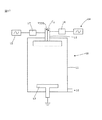
図17において、発明の実施の形態を実施する図示した装置は、一般的に10で表される。装置は、チャンバ11と、シャワーヘッド12と、ウェーハサポート13と、高周波源14と、低周波源15と、を備える。シャワーヘッド12は、二つの前駆体(TEOS及びO2)を受け入れるように配置される。整合ユニット16及び17は、高周波源14及び低周波源15に対してそれぞれ設けられ、ポンプを使った排気口(pumped outlet)18は、余分な反応ガスを除去するために設けられる。
In FIG. 17, the illustrated apparatus for implementing an embodiment of the invention is generally designated 10. The apparatus includes a
一連の実験が、装置を用いながら以下のプロセス条件下で行われた。
プロセス1−DEP:2400mT,1500sccm O2,1000sccm He,1.0ccm TEOS, 666W HF,334W LF,14mm ES(15:1)
PLAS:2000mT,1000sccm H2,1000W HF,20mm ES
プロセス2−DEP:2000mT,1500sccm O2,1000sccm He,0.66ccm TEOS, 666W HF,334W LF,14mm ES(22.7:1)
PLAS:2000mT,1000sccm H2,1000W HF,20mm ES
プロセス3−DEP:2800mT,500sccm O2,1000sccm He,1.25ccm TEOS, 900W HF,11mm ES(4:1)
プロセス4−DEP:3500mT,750sccm O2,1000sccm He,1.25ccm TEOS, 666W HF,334W LF,14mm ES(6:1)
PLAS:上記の通り、すなわち、2000mT,1000sccm H2,1000W HF,20mm ES
A series of experiments were conducted under the following process conditions using the apparatus.
Process 1-DEP: 2400 mT, 1500 sccm O 2 , 1000 sccm He, 1.0 ccm TEOS, 666 W HF, 334 W LF, 14 mm ES (15: 1)
PLAS: 2000 mT, 1000 sccm H 2 , 1000 W HF, 20 mm ES
Process 2-DEP: 2000 mT, 1500 sccm O 2 , 1000 sccm He, 0.66 ccm TEOS, 666 W HF, 334 W LF, 14 mm ES (22.7: 1)
PLAS: 2000 mT, 1000 sccm H 2 , 1000 W HF, 20 mm ES
Process 3-DEP: 2800 mT, 500 sccm O 2 , 1000 sccm He, 1.25 ccm TEOS, 900 W HF, 11 mm ES (4: 1)
Process 4-DEP: 3500 mT, 750 sccm O 2 , 1000 sccm He, 1.25 ccm TEOS, 666 W HF, 334 W LF, 14 mm ES (6: 1)
PLAS: As described above, that is, 2000 mT, 1000 sccm H 2 , 1000 W HF, 20 mm ES
処理圧力をmTで測定する場合、O2,TEOS及びHeキャリアガスの流量はsccmで表され、RF電力は、13.56MHzの高周波数及び375kHzの低周波数のときにWで測定され、電極(シャワーヘッド)と基板との間の間隔ESはmmで表す。 When the processing pressure is measured in mT, the flow rates of O 2 , TEOS and He carrier gas are expressed in sccm, and the RF power is measured in W at a high frequency of 13.56 MHz and a low frequency of 375 kHz. The distance ES between the shower head) and the substrate is expressed in mm.
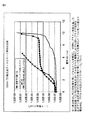
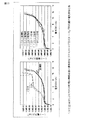
上記プロセスで説明した条件は、最初の堆積プロセス(DEP)と次のプラズマ処理(PLAS)との間で分けられる。上記圧力はチャンバ圧である。ヘリウムは、プロセスのキャリアガスとして用いられる。カッコ内の比は、TEOSに対するO2の比である。図1は、低温(200℃)で堆積した膜に対するH2プラズマ処理の効果を示す。リーク電流による破壊は、一般的に、1.00 E−07と1.00 E06との間のどこかで生じると考えられ、水素プラズマ処理された膜の破壊特性が著しく向上しているのがわかる。 The conditions described in the above process are divided between an initial deposition process (DEP) and a subsequent plasma treatment (PLAS). The pressure is a chamber pressure. Helium is used as a process carrier gas. The ratio in parentheses is the ratio of O 2 to TEOS. FIG. 1 shows the effect of H 2 plasma treatment on films deposited at low temperature (200 ° C.). The breakdown due to the leakage current is generally considered to occur somewhere between 1.00 E-07 and 1.00 E06, and the breakdown characteristics of the film treated with hydrogen plasma are remarkably improved. Recognize.
図2は、150℃で堆積した膜に対してプラズマ処理を施さない場合とプラズマ処理を施した場合との間の関係を示し、この場合も破壊特性が向上しているのがわかる。図3は、プラズマ処理が施されたときに依存する破壊特性を示し、非常に長い時間の真空破壊後でもプラズマ処理が有効であることがわかるが、24時間までの真空破壊を有するのが有利であるのがわかる。 FIG. 2 shows the relationship between the case where the film deposited at 150 ° C. is not subjected to the plasma treatment and the case where the plasma treatment is performed, and it can be seen that the destructive characteristics are also improved in this case. FIG. 3 shows the breakdown characteristics that depend on when the plasma treatment is applied, and it can be seen that the plasma treatment is effective even after a very long vacuum break, but it is advantageous to have a vacuum break of up to 24 hours. I understand that.
図4は、異なる長さのプラズマ処理を有する複数の膜に対するFTIRスペクトルを示す。プラズマ処理を施さない膜と比較すると、プラズマ処理が〜3300cm-1及び980cm-1のOHピークを除去していることがわかる。膜の表面上又はその付近にSi−H結合が存在することを表す2340cm-1での非常に小さいピークも存在し、これによって、膜が疎水性になり、膜の表面上又は膜を通過する水蒸気の吸収を減少し、膜の容積中に比較的少ないOHを有する。 FIG. 4 shows FTIR spectra for multiple films with different lengths of plasma treatment. Compared with film not subjected to plasma treatment, it can be seen that the plasma treatment is to remove the OH peak of ~3300Cm -1 and 980 cm -1. There is also a very small peak at 2340 cm −1 representing the presence of Si—H bonds on or near the surface of the membrane, which makes the membrane hydrophobic and passes on or through the membrane surface. Reduces water vapor absorption and has relatively little OH in the membrane volume.
図5及び6は、異なるタイプのアニールの効果を示し、H2プラズマ処理が再吸収の防止よりも著しく良好であることが観察される。図7は、経時的な再吸収を示す。 FIGS. 5 and 6 show the effect of different types of annealing and it is observed that the H 2 plasma treatment is significantly better than preventing reabsorption. FIG. 7 shows reabsorption over time.
したがって、これらの三つの図から、H2プラズマ処理により疎水性表面を形成することによって少なくとも部分的に膜の水分を減少させるとともに膜への再吸収の速度を減少していることがわかる。その結果、150℃の堆積温度でも優れている。したがって、この温度より下で実用的な膜を得ることができると考えられる。プラズマ処理を真空破壊後に行うことができ、そのような破壊によって膜を強化することができる。 Therefore, it can be seen from these three figures that the formation of a hydrophobic surface by H 2 plasma treatment at least partially reduces the moisture in the membrane and reduces the rate of reabsorption into the membrane. As a result, the deposition temperature of 150 ° C. is excellent. Therefore, it is considered that a practical film can be obtained below this temperature. The plasma treatment can be performed after the vacuum break and the film can be strengthened by such a break.
好適には、H2プラズマ処理温度は、低く、例えば、200℃以下、125℃又は150℃周辺である。 Preferably, the H 2 plasma treatment temperature is low, for example, around 200 ° C. or lower, around 125 ° C. or 150 ° C.
ヘリウムプラズマ処理、NH3プラズマ処理並びにH2炉アニールが同一の結果を提供しないことにも留意すべきである。 It should also be noted that helium plasma treatment, NH 3 plasma treatment and H 2 furnace anneal do not provide the same results.
図8a及び8bは、プラテン13のサポートの温度に対するステップカバレージを示す。ステップカバレージは、温度が増大するに従って及びO2/TEOS比が増大するに従って向上する。しかしながら、許容できるステップカバレージを過程的に(historically)低い温度で達成することができる。
FIGS. 8 a and 8 b show the step coverage for the temperature of the
図9は、プラズマ処理された膜のリーク電流の堆積温度の効果を示し、高温で良好な結果となるが、プラズマの許容できる結果を非常に低い温度で達成することができる。 FIG. 9 shows the effect of the deposition temperature on the leakage current of the plasma treated film, with good results at high temperatures, but acceptable results for plasma can be achieved at very low temperatures.
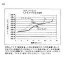
図10は、O2/TEOS比に対する堆積速度の関係を示し、比が増大するに従って堆積速度が減少することがわかる。 FIG. 10 shows the relationship of the deposition rate to the O 2 / TEOS ratio, and it can be seen that the deposition rate decreases as the ratio increases.
これまで説明したように、シャワーヘッドは、好適には混合周波数で給電され、典型的な配置は、13.56MHzの高周波数及び375kHzの低周波数である。しかしながら、低周波成分を増大して2MHzまでの周波数にすることができる。低周波成分を導入しても堆積速度が変化しないことがわかり、したがって、イオン襲撃によって膜の密度が増加するとは考えられない。図11は、低周波成分の導入による再吸収の影響を示す。この実験に対する堆積条件を、図示したRF成分の変動の影響下にあるプロセス4で説明した通りとした。混合周波数を用いたときの再吸収は単一の13.56MHzのRF源を用いた場合に比べて明らかに小さい。SiO2膜の堆積速度及び屈折率に著しい変化がないので、低周波成分がプラズマ中の気体種類を変えると考えられる。図12は、高周波数のみの場合と混合周波数の場合との間のリーク電流の差を比較する。符号Dot1,Dot2及びDot3は、ウェーハ上の異なる点の測定を表す。リーク特性の著しい向上があることがわかる。一般的に、低周波電力が存在することによってOHの再吸収が更に少なくなるとともに破壊電圧が更に高くなるということが結論付けられる。
As explained so far, the showerhead is preferably powered at a mixed frequency, with a typical arrangement being a high frequency of 13.56 MHz and a low frequency of 375 kHz. However, the low frequency component can be increased to frequencies up to 2 MHz. It can be seen that the deposition rate does not change with the introduction of low frequency components, and therefore it is unlikely that the ion attack will increase the density of the film. FIG. 11 shows the effect of reabsorption due to the introduction of low frequency components. The deposition conditions for this experiment were as described in
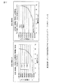
図14〜16は、異なるO2/TEOS比に対する175℃及び200℃での24時間の再吸収後の電気反応を有効に比較する。6:1の低い比において175℃での著しい再吸収があるが、比が大きくなるに従って劣化及び性能の程度が減少することがわかる。 FIGS. 14-16 effectively compare the electrical response after 24 hours reabsorption at 175 ° C. and 200 ° C. for different O 2 / TEOS ratios. It can be seen that there is significant reabsorption at 175 ° C. at a low ratio of 6: 1, but the degree of degradation and performance decreases as the ratio increases.
図16は、プロセス2における膜の良好な吸収性能を示す。
FIG. 16 shows the good absorption performance of the membrane in
上述したように、良好なリーク特性及び良好なステップカバレージを有する、200℃より下の温度で堆積された膜を、混合周波数RF電力及び理想的にはH2プラズマ処理を用いた約22:1のような比較的高いO2/TEOS比で達成できる。しかしながら、データは、これらの基準の選択を用いることによって向上した膜を達成できることも示す。 As noted above, films deposited at temperatures below 200 ° C. with good leakage characteristics and good step coverage are about 22: 1 using mixed frequency RF power and ideally H 2 plasma treatment. Can be achieved with a relatively high O 2 / TEOS ratio. However, the data also shows that improved membranes can be achieved by using these criteria selections.
膜を125℃程度の低い温度で堆積できることが予測される。 It is expected that films can be deposited at temperatures as low as 125 ° C.
Claims (9)
Applications Claiming Priority (2)
| Application Number | Priority Date | Filing Date | Title |
|---|---|---|---|
| GB0922647.3 | 2009-12-24 | ||
| GBGB0922647.3A GB0922647D0 (en) | 2009-12-24 | 2009-12-24 | Methods of depositing SiO² films |
Publications (3)
| Publication Number | Publication Date |
|---|---|
| JP2011135084A JP2011135084A (en) | 2011-07-07 |
| JP2011135084A5 JP2011135084A5 (en) | 2013-04-11 |
| JP6058876B2 true JP6058876B2 (en) | 2017-01-11 |
Family
ID=41716978
Family Applications (1)
| Application Number | Title | Priority Date | Filing Date |
|---|---|---|---|
| JP2010286580A Active JP6058876B2 (en) | 2009-12-24 | 2010-12-22 | Method for depositing SiO2 film |
Country Status (6)
| Country | Link |
|---|---|
| EP (1) | EP2362003B1 (en) |
| JP (1) | JP6058876B2 (en) |
| KR (1) | KR101472733B1 (en) |
| CN (1) | CN102108497B (en) |
| GB (1) | GB0922647D0 (en) |
| TW (1) | TWI518201B (en) |
Families Citing this family (12)
| Publication number | Priority date | Publication date | Assignee | Title |
|---|---|---|---|---|
| US8329575B2 (en) * | 2010-12-22 | 2012-12-11 | Applied Materials, Inc. | Fabrication of through-silicon vias on silicon wafers |
| GB201207448D0 (en) | 2012-04-26 | 2012-06-13 | Spts Technologies Ltd | Method of depositing silicon dioxide films |
| JP2015029004A (en) * | 2013-07-30 | 2015-02-12 | 株式会社アルバック | Plasma cvd system and film formation method |
| GB201410317D0 (en) * | 2014-06-10 | 2014-07-23 | Spts Technologies Ltd | Substrate |
| US9390910B2 (en) * | 2014-10-03 | 2016-07-12 | Applied Materials, Inc. | Gas flow profile modulated control of overlay in plasma CVD films |
| EP3354771A4 (en) * | 2015-09-21 | 2018-10-31 | Posco | Color-treated substrate and color treatment method therefor |
| KR101772772B1 (en) * | 2015-12-08 | 2017-08-29 | 주식회사 포스코 | Surface-treated substrate and preparation method thereof |
| GB201522552D0 (en) * | 2015-12-21 | 2016-02-03 | Spts Technologies Ltd | Method of improving adhesion |
| CN106783535A (en) * | 2016-11-28 | 2017-05-31 | 武汉新芯集成电路制造有限公司 | The method and semiconductor structure of a kind of improvement PETEOS film defects |
| CN108018538A (en) * | 2017-11-24 | 2018-05-11 | 中航(重庆)微电子有限公司 | The method and apparatus of silica membrane is prepared using PE-TEOS techniques |
| CN111235547B (en) * | 2020-04-27 | 2020-08-07 | 上海陛通半导体能源科技股份有限公司 | Chemical vapor deposition method |
| CN114000123A (en) * | 2021-11-02 | 2022-02-01 | 浙江光特科技有限公司 | Preparation of SiO2Method, chip and device for thin film |
Family Cites Families (11)
| Publication number | Priority date | Publication date | Assignee | Title |
|---|---|---|---|---|
| US5356722A (en) * | 1992-06-10 | 1994-10-18 | Applied Materials, Inc. | Method for depositing ozone/TEOS silicon oxide films of reduced surface sensitivity |
| DE19523442A1 (en) * | 1995-06-28 | 1997-01-02 | Antec Angewandte Neue Technolo | Production of transparent quartz-like coating on a metal surface |
| JP2973905B2 (en) * | 1995-12-27 | 1999-11-08 | 日本電気株式会社 | Method for manufacturing semiconductor device |
| US6028014A (en) * | 1997-11-10 | 2000-02-22 | Lsi Logic Corporation | Plasma-enhanced oxide process optimization and material and apparatus therefor |
| JP3933793B2 (en) * | 1998-06-16 | 2007-06-20 | 富士通株式会社 | Method for forming silicon oxide film and method for manufacturing thin film magnetic head |
| JP3248492B2 (en) * | 1998-08-14 | 2002-01-21 | 日本電気株式会社 | Semiconductor device and manufacturing method thereof |
| JP3184177B2 (en) * | 1999-03-26 | 2001-07-09 | キヤノン販売株式会社 | Method for forming interlayer insulating film, semiconductor manufacturing apparatus, and semiconductor device |
| US7247252B2 (en) * | 2002-06-20 | 2007-07-24 | Taiwan Semiconductor Manufacturing Co., Ltd. | Method of avoiding plasma arcing during RIE etching |
| JP2005150299A (en) * | 2003-11-13 | 2005-06-09 | Seiko Epson Corp | Semiconductor chip, semiconductor device, method of manufacturing the same, circuit board, and electronic equipment |
| US7888273B1 (en) * | 2006-11-01 | 2011-02-15 | Novellus Systems, Inc. | Density gradient-free gap fill |
| JP4985411B2 (en) * | 2008-01-08 | 2012-07-25 | 住友電気工業株式会社 | Method for fabricating a semiconductor optical device |
-
2009
- 2009-12-24 GB GBGB0922647.3A patent/GB0922647D0/en not_active Ceased
-
2010
- 2010-12-20 EP EP10275131.0A patent/EP2362003B1/en active Active
- 2010-12-20 TW TW099144743A patent/TWI518201B/en active
- 2010-12-22 JP JP2010286580A patent/JP6058876B2/en active Active
- 2010-12-24 CN CN201010615668.9A patent/CN102108497B/en active Active
- 2010-12-24 KR KR1020100134279A patent/KR101472733B1/en active IP Right Grant
Also Published As
| Publication number | Publication date |
|---|---|
| JP2011135084A (en) | 2011-07-07 |
| CN102108497A (en) | 2011-06-29 |
| EP2362003A3 (en) | 2011-09-07 |
| CN102108497B (en) | 2015-07-15 |
| KR101472733B1 (en) | 2014-12-15 |
| GB0922647D0 (en) | 2010-02-10 |
| EP2362003A2 (en) | 2011-08-31 |
| KR20110074478A (en) | 2011-06-30 |
| EP2362003B1 (en) | 2017-07-05 |
| TW201139719A (en) | 2011-11-16 |
| TWI518201B (en) | 2016-01-21 |
Similar Documents
| Publication | Publication Date | Title |
|---|---|---|
| JP6058876B2 (en) | Method for depositing SiO2 film | |
| US7989365B2 (en) | Remote plasma source seasoning | |
| US9018108B2 (en) | Low shrinkage dielectric films | |
| US7435684B1 (en) | Resolving of fluorine loading effect in the vacuum chamber | |
| US8889566B2 (en) | Low cost flowable dielectric films | |
| KR101528832B1 (en) | Manufacturing method of flowable dielectric layer | |
| US7888273B1 (en) | Density gradient-free gap fill | |
| US7807566B2 (en) | Method for forming dielectric SiOCH film having chemical stability | |
| US10096466B2 (en) | Pulsed plasma for film deposition | |
| US8466067B2 (en) | Post-planarization densification | |
| US9165762B2 (en) | Method of depositing silicone dioxide films | |
| US20140186544A1 (en) | Metal processing using high density plasma | |
| US20130288485A1 (en) | Densification for flowable films | |
| KR20080107270A (en) | Method for forming inorganic silazane-based dielectric film | |
| JP2001507081A (en) | Inductively coupled plasma CVD | |
| JP2001267310A (en) | Method and device for film forming plasma | |
| US20110318502A1 (en) | Methods of depositing sio2 films | |
| US20100003833A1 (en) | Method of forming fluorine-containing dielectric film | |
| KR20140086607A (en) | Thin film deposition method with high speed and apparatus for the same | |
| JPH098029A (en) | Insulation film containing fluorine and formation thereof |
Legal Events
| Date | Code | Title | Description |
|---|---|---|---|
| A521 | Request for written amendment filed |
Free format text: JAPANESE INTERMEDIATE CODE: A523 Effective date: 20130222 |
|
| A621 | Written request for application examination |
Free format text: JAPANESE INTERMEDIATE CODE: A621 Effective date: 20130222 |
|
| A131 | Notification of reasons for refusal |
Free format text: JAPANESE INTERMEDIATE CODE: A131 Effective date: 20140401 |
|
| A521 | Request for written amendment filed |
Free format text: JAPANESE INTERMEDIATE CODE: A523 Effective date: 20140701 |
|
| A02 | Decision of refusal |
Free format text: JAPANESE INTERMEDIATE CODE: A02 Effective date: 20150303 |
|
| A521 | Request for written amendment filed |
Free format text: JAPANESE INTERMEDIATE CODE: A523 Effective date: 20150703 |
|
| A521 | Request for written amendment filed |
Free format text: JAPANESE INTERMEDIATE CODE: A821 Effective date: 20150707 |
|
| A911 | Transfer to examiner for re-examination before appeal (zenchi) |
Free format text: JAPANESE INTERMEDIATE CODE: A911 Effective date: 20150907 |
|
| A912 | Re-examination (zenchi) completed and case transferred to appeal board |
Free format text: JAPANESE INTERMEDIATE CODE: A912 Effective date: 20151113 |
|
| A521 | Request for written amendment filed |
Free format text: JAPANESE INTERMEDIATE CODE: A523 Effective date: 20160915 |
|
| A61 | First payment of annual fees (during grant procedure) |
Free format text: JAPANESE INTERMEDIATE CODE: A61 Effective date: 20161208 |
|
| R150 | Certificate of patent or registration of utility model |
Ref document number: 6058876 Country of ref document: JP Free format text: JAPANESE INTERMEDIATE CODE: R150 |
|
| R250 | Receipt of annual fees |
Free format text: JAPANESE INTERMEDIATE CODE: R250 |
|
| R250 | Receipt of annual fees |
Free format text: JAPANESE INTERMEDIATE CODE: R250 |
|
| R250 | Receipt of annual fees |
Free format text: JAPANESE INTERMEDIATE CODE: R250 |
|
| R250 | Receipt of annual fees |
Free format text: JAPANESE INTERMEDIATE CODE: R250 |
|
| R250 | Receipt of annual fees |
Free format text: JAPANESE INTERMEDIATE CODE: R250 |