EP2362003B1 - Method of depositing SiO2 films - Google Patents
Method of depositing SiO2 films Download PDFInfo
- Publication number
- EP2362003B1 EP2362003B1 EP10275131.0A EP10275131A EP2362003B1 EP 2362003 B1 EP2362003 B1 EP 2362003B1 EP 10275131 A EP10275131 A EP 10275131A EP 2362003 B1 EP2362003 B1 EP 2362003B1
- Authority
- EP
- European Patent Office
- Prior art keywords
- teos
- film
- plasma
- frequency component
- plasma treatment
- Prior art date
- Legal status (The legal status is an assumption and is not a legal conclusion. Google has not performed a legal analysis and makes no representation as to the accuracy of the status listed.)
- Active
Links
- 238000000034 method Methods 0.000 title claims description 35
- 238000000151 deposition Methods 0.000 title claims description 29
- VYPSYNLAJGMNEJ-UHFFFAOYSA-N Silicium dioxide Chemical compound O=[Si]=O VYPSYNLAJGMNEJ-UHFFFAOYSA-N 0.000 title claims description 16
- 229910052681 coesite Inorganic materials 0.000 title claims description 8
- 229910052906 cristobalite Inorganic materials 0.000 title claims description 8
- 239000000377 silicon dioxide Substances 0.000 title claims description 8
- 229910052682 stishovite Inorganic materials 0.000 title claims description 8
- 229910052905 tridymite Inorganic materials 0.000 title claims description 8
- 235000012239 silicon dioxide Nutrition 0.000 title 1
- BOTDANWDWHJENH-UHFFFAOYSA-N Tetraethyl orthosilicate Chemical compound CCO[Si](OCC)(OCC)OCC BOTDANWDWHJENH-UHFFFAOYSA-N 0.000 claims description 46
- 238000009832 plasma treatment Methods 0.000 claims description 27
- 238000005334 plasma enhanced chemical vapour deposition Methods 0.000 claims description 11
- 238000000623 plasma-assisted chemical vapour deposition Methods 0.000 claims description 11
- 239000002243 precursor Substances 0.000 claims description 10
- 230000001419 dependent effect Effects 0.000 claims 2
- 230000008021 deposition Effects 0.000 description 24
- 230000008569 process Effects 0.000 description 20
- 238000011282 treatment Methods 0.000 description 8
- 230000015556 catabolic process Effects 0.000 description 6
- 238000005137 deposition process Methods 0.000 description 6
- 238000010521 absorption reaction Methods 0.000 description 5
- 238000001157 Fourier transform infrared spectrum Methods 0.000 description 4
- 230000000694 effects Effects 0.000 description 4
- 230000004044 response Effects 0.000 description 4
- FFBHFFJDDLITSX-UHFFFAOYSA-N benzyl N-[2-hydroxy-4-(3-oxomorpholin-4-yl)phenyl]carbamate Chemical compound OC1=C(NC(=O)OCC2=CC=CC=C2)C=CC(=C1)N1CCOCC1=O FFBHFFJDDLITSX-UHFFFAOYSA-N 0.000 description 3
- 230000008859 change Effects 0.000 description 3
- 238000005033 Fourier transform infrared spectroscopy Methods 0.000 description 2
- UFHFLCQGNIYNRP-UHFFFAOYSA-N Hydrogen Chemical compound [H][H] UFHFLCQGNIYNRP-UHFFFAOYSA-N 0.000 description 2
- XUIMIQQOPSSXEZ-UHFFFAOYSA-N Silicon Chemical compound [Si] XUIMIQQOPSSXEZ-UHFFFAOYSA-N 0.000 description 2
- 239000012159 carrier gas Substances 0.000 description 2
- 238000002474 experimental method Methods 0.000 description 2
- 239000007789 gas Substances 0.000 description 2
- 239000001307 helium Substances 0.000 description 2
- 229910052734 helium Inorganic materials 0.000 description 2
- SWQJXJOGLNCZEY-UHFFFAOYSA-N helium atom Chemical compound [He] SWQJXJOGLNCZEY-UHFFFAOYSA-N 0.000 description 2
- 239000001257 hydrogen Substances 0.000 description 2
- 229910052739 hydrogen Inorganic materials 0.000 description 2
- 125000002496 methyl group Chemical group [H]C([H])([H])* 0.000 description 2
- 229910052710 silicon Inorganic materials 0.000 description 2
- 239000010703 silicon Substances 0.000 description 2
- 238000001228 spectrum Methods 0.000 description 2
- 101150073458 DOT1 gene Proteins 0.000 description 1
- 101100278332 Dictyostelium discoideum dotA gene Proteins 0.000 description 1
- 229910020177 SiOF Inorganic materials 0.000 description 1
- BLRPTPMANUNPDV-UHFFFAOYSA-N Silane Chemical compound [SiH4] BLRPTPMANUNPDV-UHFFFAOYSA-N 0.000 description 1
- 239000002250 absorbent Substances 0.000 description 1
- 230000002745 absorbent Effects 0.000 description 1
- 230000008901 benefit Effects 0.000 description 1
- 238000012512 characterization method Methods 0.000 description 1
- 238000006243 chemical reaction Methods 0.000 description 1
- 230000007423 decrease Effects 0.000 description 1
- 230000006866 deterioration Effects 0.000 description 1
- 125000001301 ethoxy group Chemical group [H]C([H])([H])C([H])([H])O* 0.000 description 1
- 230000002209 hydrophobic effect Effects 0.000 description 1
- 230000005661 hydrophobic surface Effects 0.000 description 1
- 230000006872 improvement Effects 0.000 description 1
- 238000010348 incorporation Methods 0.000 description 1
- 238000010849 ion bombardment Methods 0.000 description 1
- 150000002605 large molecules Chemical class 0.000 description 1
- 229920002521 macromolecule Polymers 0.000 description 1
- 238000005259 measurement Methods 0.000 description 1
- 238000002360 preparation method Methods 0.000 description 1
- 238000000926 separation method Methods 0.000 description 1
- 239000000758 substrate Substances 0.000 description 1
- 230000000007 visual effect Effects 0.000 description 1
- XLYOFNOQVPJJNP-UHFFFAOYSA-N water Substances O XLYOFNOQVPJJNP-UHFFFAOYSA-N 0.000 description 1
Images


Classifications
-
- C—CHEMISTRY; METALLURGY
- C23—COATING METALLIC MATERIAL; COATING MATERIAL WITH METALLIC MATERIAL; CHEMICAL SURFACE TREATMENT; DIFFUSION TREATMENT OF METALLIC MATERIAL; COATING BY VACUUM EVAPORATION, BY SPUTTERING, BY ION IMPLANTATION OR BY CHEMICAL VAPOUR DEPOSITION, IN GENERAL; INHIBITING CORROSION OF METALLIC MATERIAL OR INCRUSTATION IN GENERAL
- C23C—COATING METALLIC MATERIAL; COATING MATERIAL WITH METALLIC MATERIAL; SURFACE TREATMENT OF METALLIC MATERIAL BY DIFFUSION INTO THE SURFACE, BY CHEMICAL CONVERSION OR SUBSTITUTION; COATING BY VACUUM EVAPORATION, BY SPUTTERING, BY ION IMPLANTATION OR BY CHEMICAL VAPOUR DEPOSITION, IN GENERAL
- C23C16/00—Chemical coating by decomposition of gaseous compounds, without leaving reaction products of surface material in the coating, i.e. chemical vapour deposition [CVD] processes
- C23C16/22—Chemical coating by decomposition of gaseous compounds, without leaving reaction products of surface material in the coating, i.e. chemical vapour deposition [CVD] processes characterised by the deposition of inorganic material, other than metallic material
- C23C16/30—Deposition of compounds, mixtures or solid solutions, e.g. borides, carbides, nitrides
- C23C16/40—Oxides
- C23C16/401—Oxides containing silicon
- C23C16/402—Silicon dioxide
-
- C—CHEMISTRY; METALLURGY
- C23—COATING METALLIC MATERIAL; COATING MATERIAL WITH METALLIC MATERIAL; CHEMICAL SURFACE TREATMENT; DIFFUSION TREATMENT OF METALLIC MATERIAL; COATING BY VACUUM EVAPORATION, BY SPUTTERING, BY ION IMPLANTATION OR BY CHEMICAL VAPOUR DEPOSITION, IN GENERAL; INHIBITING CORROSION OF METALLIC MATERIAL OR INCRUSTATION IN GENERAL
- C23C—COATING METALLIC MATERIAL; COATING MATERIAL WITH METALLIC MATERIAL; SURFACE TREATMENT OF METALLIC MATERIAL BY DIFFUSION INTO THE SURFACE, BY CHEMICAL CONVERSION OR SUBSTITUTION; COATING BY VACUUM EVAPORATION, BY SPUTTERING, BY ION IMPLANTATION OR BY CHEMICAL VAPOUR DEPOSITION, IN GENERAL
- C23C16/00—Chemical coating by decomposition of gaseous compounds, without leaving reaction products of surface material in the coating, i.e. chemical vapour deposition [CVD] processes
- C23C16/44—Chemical coating by decomposition of gaseous compounds, without leaving reaction products of surface material in the coating, i.e. chemical vapour deposition [CVD] processes characterised by the method of coating
- C23C16/455—Chemical coating by decomposition of gaseous compounds, without leaving reaction products of surface material in the coating, i.e. chemical vapour deposition [CVD] processes characterised by the method of coating characterised by the method used for introducing gases into reaction chamber or for modifying gas flows in reaction chamber
- C23C16/45563—Gas nozzles
- C23C16/45565—Shower nozzles
-
- C—CHEMISTRY; METALLURGY
- C23—COATING METALLIC MATERIAL; COATING MATERIAL WITH METALLIC MATERIAL; CHEMICAL SURFACE TREATMENT; DIFFUSION TREATMENT OF METALLIC MATERIAL; COATING BY VACUUM EVAPORATION, BY SPUTTERING, BY ION IMPLANTATION OR BY CHEMICAL VAPOUR DEPOSITION, IN GENERAL; INHIBITING CORROSION OF METALLIC MATERIAL OR INCRUSTATION IN GENERAL
- C23C—COATING METALLIC MATERIAL; COATING MATERIAL WITH METALLIC MATERIAL; SURFACE TREATMENT OF METALLIC MATERIAL BY DIFFUSION INTO THE SURFACE, BY CHEMICAL CONVERSION OR SUBSTITUTION; COATING BY VACUUM EVAPORATION, BY SPUTTERING, BY ION IMPLANTATION OR BY CHEMICAL VAPOUR DEPOSITION, IN GENERAL
- C23C16/00—Chemical coating by decomposition of gaseous compounds, without leaving reaction products of surface material in the coating, i.e. chemical vapour deposition [CVD] processes
- C23C16/44—Chemical coating by decomposition of gaseous compounds, without leaving reaction products of surface material in the coating, i.e. chemical vapour deposition [CVD] processes characterised by the method of coating
- C23C16/50—Chemical coating by decomposition of gaseous compounds, without leaving reaction products of surface material in the coating, i.e. chemical vapour deposition [CVD] processes characterised by the method of coating using electric discharges
- C23C16/505—Chemical coating by decomposition of gaseous compounds, without leaving reaction products of surface material in the coating, i.e. chemical vapour deposition [CVD] processes characterised by the method of coating using electric discharges using radio frequency discharges
-
- C—CHEMISTRY; METALLURGY
- C23—COATING METALLIC MATERIAL; COATING MATERIAL WITH METALLIC MATERIAL; CHEMICAL SURFACE TREATMENT; DIFFUSION TREATMENT OF METALLIC MATERIAL; COATING BY VACUUM EVAPORATION, BY SPUTTERING, BY ION IMPLANTATION OR BY CHEMICAL VAPOUR DEPOSITION, IN GENERAL; INHIBITING CORROSION OF METALLIC MATERIAL OR INCRUSTATION IN GENERAL
- C23C—COATING METALLIC MATERIAL; COATING MATERIAL WITH METALLIC MATERIAL; SURFACE TREATMENT OF METALLIC MATERIAL BY DIFFUSION INTO THE SURFACE, BY CHEMICAL CONVERSION OR SUBSTITUTION; COATING BY VACUUM EVAPORATION, BY SPUTTERING, BY ION IMPLANTATION OR BY CHEMICAL VAPOUR DEPOSITION, IN GENERAL
- C23C16/00—Chemical coating by decomposition of gaseous compounds, without leaving reaction products of surface material in the coating, i.e. chemical vapour deposition [CVD] processes
- C23C16/44—Chemical coating by decomposition of gaseous compounds, without leaving reaction products of surface material in the coating, i.e. chemical vapour deposition [CVD] processes characterised by the method of coating
- C23C16/52—Controlling or regulating the coating process
-
- C—CHEMISTRY; METALLURGY
- C23—COATING METALLIC MATERIAL; COATING MATERIAL WITH METALLIC MATERIAL; CHEMICAL SURFACE TREATMENT; DIFFUSION TREATMENT OF METALLIC MATERIAL; COATING BY VACUUM EVAPORATION, BY SPUTTERING, BY ION IMPLANTATION OR BY CHEMICAL VAPOUR DEPOSITION, IN GENERAL; INHIBITING CORROSION OF METALLIC MATERIAL OR INCRUSTATION IN GENERAL
- C23C—COATING METALLIC MATERIAL; COATING MATERIAL WITH METALLIC MATERIAL; SURFACE TREATMENT OF METALLIC MATERIAL BY DIFFUSION INTO THE SURFACE, BY CHEMICAL CONVERSION OR SUBSTITUTION; COATING BY VACUUM EVAPORATION, BY SPUTTERING, BY ION IMPLANTATION OR BY CHEMICAL VAPOUR DEPOSITION, IN GENERAL
- C23C16/00—Chemical coating by decomposition of gaseous compounds, without leaving reaction products of surface material in the coating, i.e. chemical vapour deposition [CVD] processes
- C23C16/56—After-treatment
-
- H—ELECTRICITY
- H01—ELECTRIC ELEMENTS
- H01L—SEMICONDUCTOR DEVICES NOT COVERED BY CLASS H10
- H01L21/00—Processes or apparatus adapted for the manufacture or treatment of semiconductor or solid state devices or of parts thereof
- H01L21/02—Manufacture or treatment of semiconductor devices or of parts thereof
- H01L21/02104—Forming layers
- H01L21/02365—Forming inorganic semiconducting materials on a substrate
- H01L21/02612—Formation types
- H01L21/02617—Deposition types
- H01L21/0262—Reduction or decomposition of gaseous compounds, e.g. CVD
-
- H—ELECTRICITY
- H01—ELECTRIC ELEMENTS
- H01L—SEMICONDUCTOR DEVICES NOT COVERED BY CLASS H10
- H01L21/00—Processes or apparatus adapted for the manufacture or treatment of semiconductor or solid state devices or of parts thereof
- H01L21/67—Apparatus specially adapted for handling semiconductor or electric solid state devices during manufacture or treatment thereof; Apparatus specially adapted for handling wafers during manufacture or treatment of semiconductor or electric solid state devices or components ; Apparatus not specifically provided for elsewhere
- H01L21/67005—Apparatus not specifically provided for elsewhere
- H01L21/67011—Apparatus for manufacture or treatment
- H01L21/67155—Apparatus for manufacturing or treating in a plurality of work-stations
- H01L21/67207—Apparatus for manufacturing or treating in a plurality of work-stations comprising a chamber adapted to a particular process
Definitions
- This invention relates to a method of depositing SiO 2 films and in particular to depositing such films below 250°C using plasma enhanced chemical vapour deposition (PECVD) according to claim 1.
- PECVD plasma enhanced chemical vapour deposition
- TSVs Through silicon vias (TSVs), which can for example be etched vias or trenches in silicon, require a dielectric liner prior to metallic layer deposition. It is highly desirable that such films are good conformal films because of their minimum thickness the dielectric properties have to be good enough to avoid current leakage in normal use. There also has to be limited, if any, moisture absorption following the depositions step, particularly as quite commonly the next step will follow a vacuum break. It is also desirable that they can be deposited at low temperatures, preferably below even 200°C whilst being conformal and non absorbent.
- PECVD using TEOS/O 2 precursors have been considered because they have generally good step coverage and the cost of the precursors is relatively low. However, when deposition temperatures are reduced to less than 200°C to 250°C the dielectric properties (leakage and ultimate breakdown) become degraded.
- an article entitled Characterisation and Preparation SiO 2 and SiOF films using RF PECVD technique from TEOS 2 and TEOS/O 2 /CF 4 Precursors by Kim et al - J. Phys. D: Appl. Phs. 37 (2004) 2425-2431 - the authors describe films formed from TEOS/O 2 precursors using different ratios of flow rate for the precursors.
- the invention consists in a method depositing an inorganic, dielectric SiO 2 film that temperatures below 250°C using plasma enhanced chemical vapour deposition (PECVD) in a chamber including supplying tetraethyl orthosilicate (TEOS) and O 2 , or a source thereof, as precursors, with an O 2 /TEOS ratio of between 15:1 and 25:1; wherein the precursors are deposited using an RF driven showerhead, wherein the showerhead is driven using a high frequency component and a low frequency component; and the high frequency component is at 13.56 MHz and the low frequency component is 350 kHz - 2 MHz.
- the power supplied at the high frequency component may be approximately twice the power of the low frequency component.
- the deposited film is inorganic and, specifically, one that includes no methyl groups. This means that they benefit from improved dielectric properties over films containing such groups, whilst benefitting from the conformal properties resulting from the large molecules of the TEOS precursor.
- the method may include performing a H 2 plasma treatment on the as deposited film. This treatment may be performed after a vacuum break. It is preferred that the H 2 plasma treatment is sufficient to reform Si-H bonds on the surface of the film.
- the film may be deposited at temperatures of the range 150°C to 200°C.
- a single RF frequency may be used for the H 2 plasma, where the single RF frequency may be 13.56 MHz.
- the H 2 plasma temperature may be in the range of 125 °C to 200 °C.
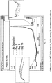
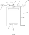
- FIG. 17 a schematic apparatus for performing the embodiments of the invention is generally illustrated at 10. It comprises a chamber 11, a showerhead 12, a waversupport 13 and respective high and low frequency sources 14 and 15.
- the showerhead 12 is arranged to receive two precursors (TEOS and O 2 ).
- Matching units 16 and 17 are provided for the high and low frequency sources 14 and 15 respectively and a pumped outlet 18 is provided for removing surplus reaction gases.
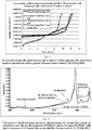
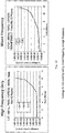
- Figure 2 illustrates at the relationship between no plasma treatment and plasma treatment on films deposited at 150°C and it is again seen that the breakdown characteristics are improved.
- Figure 3 similarly illustrates such characteristics in dependence on when the plasma treatment takes place and it would be seen that it is effective even after quite a lengthy vacuum break but that it seems to be advantageous to have a vacuum break at least up until 24 hours.
- Figure 4 shows the FTIR spectra for a number of films having different lengths of the plasma treatment.
- the plasma treatment removes OH peaks at ⁇ 3300 and 980CM -1 .
- There is also a very small peak at 2340CM -1 which indicates the presence of Si-H bonds on more near the surface of the film which would make the film hydrophobic and reduce absorption of water vapour on or through the surface of the film, which has relative little OH in its bulk.
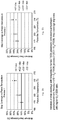
- Figures 5 and 6 illustrate the effect of different types of anneals and it would be observed that the H 2 plasma treatment is significantly better than preventing reabsorbtion.
- Figure 7 looks at the reabsorbtion over time.
- the H 2 plasma treatment reduces the moisture in the film and reduces the rate of reabsorbtion into the film, probably, at least in part, by creating a hydrophobic surface.
- the results are excellent even at a deposition temperature of 150°C. It is therefore likely that serviceable films can be obtained below this temperature.
- the treatment can be carried out after a vacuum break and they possibly be enhanced by such a break.
- the H 2 plasma treatment temperature is low, for example, 200°C or even lower, around 125°C or 150°C.
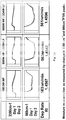
- Figures 8a and 8b show the step coverage against the temperature of the support of platen 13.
- the step coverage improves as temperature is increased and as the O 2 /TEOS ratio is increased.
- acceptable step coverage can be achieved at historically low temperatures.
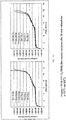
- Figure 9 shows the effect of deposition temperature on the leakage current of a plasma treated film and it will be seen that the results are better at high temperature but with the plasma acceptable results can be achieved at quite low temperatures.
- Figure 10 illustrates the relationship of deposition rate to 0 2 /TEOS ratio and it would be seen that the deposition rate falls as the ratio is increased.
- the showerhead is preferably powered at mixed frequencies and a typical arrangement is a high frequency of 13.56MHz and a low frequency of 375kHz. It is however believed that the low frequency component could be increased in frequency at least up until 2MHz. It has been determined that the introduction of the low frequency component does not change the deposition rate and therefore is not believed to be increasing the density of the film by ion bombardment.
- Figure 11 shows the effect of introducing the low frequency component on reabsorbtion.
- the deposition conditions for this experiment were as set out in process 4 subject to the variation in the RF components indicated in the figure. There is visibly less reabsorbtion when mixed frequency is used as opposed to a single 13.56MHz RF source.
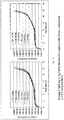
- Figure 12 compares the difference in leakage current between high frequency only and mixed frequency.
- the references to dot1, dot2, and dot3 indicate measurements at different points on the waver. It will be seen that there is a significant improvement in the leakage characteristics. In general it can be concluded that the presence of the low frequency power provides less OH reabsorbtion and a higher breakdown voltage.
- Figures 14 to 16 effectively compare the electrical response after 24 hours reabsorbtion at 175°C and 200°C for different O 2 /TEOS ratios. It would be seen that at the low ratio of 6:1 there is significant reabsorbtion at 175°C but the extent of the deterioration and performance decreases when the ratio is increased.
- Figure 16 illustrates the good absorbtion performance of a process 2 film.
- films may be deposited at temperatures as low as 125°C.
Description
- This invention relates to a method of depositing SiO2 films and in particular to depositing such films below 250°C using plasma enhanced chemical vapour deposition (PECVD) according to
claim 1. Through silicon vias (TSVs), which can for example be etched vias or trenches in silicon, require a dielectric liner prior to metallic layer deposition. It is highly desirable that such films are good conformal films because of their minimum thickness the dielectric properties have to be good enough to avoid current leakage in normal use. There also has to be limited, if any, moisture absorption following the depositions step, particularly as quite commonly the next step will follow a vacuum break. It is also desirable that they can be deposited at low temperatures, preferably below even 200°C whilst being conformal and non absorbent. - PECVD using TEOS/O2 precursors have been considered because they have generally good step coverage and the cost of the precursors is relatively low. However, when deposition temperatures are reduced to less than 200°C to 250°C the dielectric properties (leakage and ultimate breakdown) become degraded. In an article entitled Characterisation and Preparation SiO2 and SiOF films using RF PECVD technique from TEOS2 and TEOS/O2/CF4 Precursors by Kim et al - J. Phys. D: Appl. Phs. 37 (2004) 2425-2431- the authors describe films formed from TEOS/O2 precursors using different ratios of flow rate for the precursors. It will be noted that in
Figure 1 a , of that article, the deposition rate at 200°C falls dramatically and at lower ratios of O2/TEOS the authors report the incorporation of ethoxy groups into the film. They provide no information about the electrical breakdown characteristics of the films. It will be particularly noted that they report increasing O-H absorption into the film when it is exposed to air after deposition as lower deposition temperatures are used. The invention consists in a method depositing an inorganic, dielectric SiO2 film that temperatures below 250°C using plasma enhanced chemical vapour deposition (PECVD) in a chamber including supplying tetraethyl orthosilicate (TEOS) and O2, or a source thereof, as precursors, with an O2/TEOS ratio of between 15:1 and 25:1; wherein the precursors are deposited using an RF driven showerhead, wherein the showerhead is driven using a high frequency component and a low frequency component; and the high frequency component is at 13.56 MHz and the low frequency component is 350 kHz - 2 MHz. The power supplied at the high frequency component may be approximately twice the power of the low frequency component. - The Applicants have found that surprisingly, the deposited film is inorganic and, specifically, one that includes no methyl groups. This means that they benefit from improved dielectric properties over films containing such groups, whilst benefitting from the conformal properties resulting from the large molecules of the TEOS precursor.
- The method may include performing a H2 plasma treatment on the as deposited film. This treatment may be performed after a vacuum break. It is preferred that the H2 plasma treatment is sufficient to reform Si-H bonds on the surface of the film.
- In any of the above methods, the film may be deposited at temperatures of the
range 150°C to 200°C. - A single RF frequency may be used for the H2 plasma, where the single RF frequency may be 13.56 MHz. The H2 plasma temperature may be in the range of 125 °C to 200 °C.
- The invention may be performed in various ways and specific embodiments will now be described, by way of example, with reference to the accompanying drawings in which:
-
Figure 1 shows electrical characteristics of three identical thicknesses of deposited SiO2 created using a mixed frequency SiH4 PECVD deposition and mixed frequency TEOS PECVD depositions with and without a 60 s H2 plasma treatment.Process 4 used. (6:1 O2/TEOS @ 200C.); -
Figure 2 shows electrical characteristics of three identical thicknesses of deposited SiO2, created using a mixed frequency TEOS PECVD depositions with and without a 60 s H2 plasma treatment.Process 2 used. (22.7:1 O2/TEOS @ 150C.); -
Figure 3 shows the electrical leakage with applied field strength for identical TEOS/O2 deposited films with different lengths of vacuum break before H2 plasma treatment.Process 4 used (6:1 O2/TEOS @200C); -
Figure 4 shows FTIR spectra of TEOS/O2 film before and after H2 plasma treatment (60,120 and 180sec). Spectra are overlaid as a visual aid. Note the broad peak 3100-3500cm-1 and the flat region 900-1000 cm-1, both due to the presence of O-H bonds in the as deposited film.Process 4 used (6:1 O2/TEOS @ 200C); -
Figure 5 shows the electrical leakage with field voltage for various plasma and thermal post deposition treatments of TEOS films. All depositions were performed at 200°C platen. All post deposition treatments were performed insitu except for the 400°C thermal anneal treatment which was performed in a separate module (without a vacuum break); -
Figure 6 shows FTIR data from various plasma and thermal post deposition treatments of TEOS films. All depositions were performed at 200°C platen. All post deposition treatments were performed insitu except for the 400°C thermal anneal treatment which was performed in a separate module (without a vacuum break). Spectra are offset for clarity. Note weak peak at 2340cm-1 for H2 plasma and 400°C H2 anneal; -
Figures 7 shows FTIR spectra of a 150°C TEOS film (6:1 O2/TEOS) showing OH content increasing with time; -
Figure 8a and 8b show variation of a step coverage with temperature for two TEOS processes (with identical hydrogen plasma treatment) Process 1 (15:1 O2/TEOS) and process 2 (22.7:1 O2/TEOS). Step coverage improves with higher O2/TEOS ratio; -
Figure 9 shows electrical characteristics of unmodified TEOS process deposited at platen temperatures of 150-250°C (O2/TEOS 6:1) after 24hrs exposure to atmosphere; -
Figure 10 shows deposition rates as a function of O2/TEOS ration for 22.7:1 O2/TEOS process at 175°C. The refractive index (RI) remains between 1.461-1.469 for all conditions; -
Figure 11 shows moisture re-absorption as measured by change in 3300cm-1 and 980cm-1 FTIR peaks; -
Figure 12 shows leakage is improved by using mixed frequency vs high frequency; -
Figure 13 shows standard (process 4) TEOS (6:1 O2/TEOS) film electrical response after 24 hour reabsorbtion at 175 (left) and 200°C; -
Figure 14 showsprocess 1 TEOS (15:1 O2/TEOS) film electrical response after 24 hour reabsorbtion at 175°C and 200°C; -
Figure 15 showsprocess 2 TEOS(22.7:1 O2/TEOS) film electrical response after 24 hour reabsorbtion at 175 (left) and 200°C; -
Figure 16 showsprocess 2 TEOS(22.7:1 O2/TEOS, 175°C) film FTIR spectra, no change in 980 cm-1 region after 5 days. Indicative of no-moisture absorption. -
Figure 17 is a schematic drawing of the apparatus used for deposition. - In
Figure 17 a schematic apparatus for performing the embodiments of the invention is generally illustrated at 10. It comprises achamber 11, ashowerhead 12, awaversupport 13 and respective high andlow frequency sources showerhead 12 is arranged to receive two precursors (TEOS and O2).Matching units low frequency sources outlet 18 is provided for removing surplus reaction gases. - Using an apparatus a series of experiments were carried out using the following process conditions:
- Process 1 - DEP: 320 Pa (2400 mT), 1500 sccm O2, 1000 sccm He, 1.0 ccm TEOS, 666 W HF, 334 W LF, 14 mm ES (15:1) PLAS: 267 Pa (2000 mT), 1000 sccm H2, 1000 W HF, 20 mm ES
- Process 2 - DEP: 267 Pa (2000 mT), 1500 sccm O2, 1000 sccm He, 0.66 ccm TEOS, 666 W HF, 334 W LF, 14 mm ES (22.7:1) PLAS: 2000 mT, 1000 sccm H2, 1000 W HF, 20 mm ES
- Process 3 - DEP: 373 Pa (2800 mT), 500 sccm O2, 1000 sccm He, 1.25 ccm TEOS, 900 W HF, 11 mm ES (4:1)
- Process 4 - DEP: 467 Pa (3500 mT), 750 sccm O2, 1000 sccm He, 1.25 ccm TEOS, 666 W HF, 334W LF, 14 mm ES (6:1) PLAS: as described or 267 Pa (2000 mT), 1000 sccm H2, 1000 W HF, 20 mm ES
- Where the process pressure is measured in mT, the O2, TEOS and He carrier gas flows are in sccm, RF power is measured in watts with HF being 13.56MHz and LF at 375kHZ and the electrode (showerhead) to substrate separation ES is in mm
The conditions set out in the above processes are split between an initial deposition process (DEP) and a subsequent plasma treatment (PLAS). The pressure given is the chamber pressure. The helium is used as the process carrier gas. The ratio given in brackets is the ratio off O2 to TEOS.Figure 1 shows the effect of H2 plasma treatment on alow temperature 200°C) deposited film. Leakage breakdown is generally regarded as occurring somewhere between 1.00 E-07 and 1.00 E-06 and it would be seen that the hydrogen plasma treated film has significantly improved the breakdown of characteristics. -
Figure 2 illustrates at the relationship between no plasma treatment and plasma treatment on films deposited at 150°C and it is again seen that the breakdown characteristics are improved.Figure 3 similarly illustrates such characteristics in dependence on when the plasma treatment takes place and it would be seen that it is effective even after quite a lengthy vacuum break but that it seems to be advantageous to have a vacuum break at least up until 24 hours. -
Figure 4 shows the FTIR spectra for a number of films having different lengths of the plasma treatment. When compared with the film having no plasma treatment it would be seen that the plasma treatment removes OH peaks at ∼3300 and 980CM-1. There is also a very small peak at 2340CM-1 which indicates the presence of Si-H bonds on more near the surface of the film which would make the film hydrophobic and reduce absorption of water vapour on or through the surface of the film, which has relative little OH in its bulk. It will be noted that there is an absence of any peaks ∼1260cm-1 (Si-CH3) and ∼3000cm-1 (C-H). This illustrates the inorganic nature of the film. -
Figures 5 and 6 illustrate the effect of different types of anneals and it would be observed that the H2 plasma treatment is significantly better than preventing reabsorbtion.Figure 7 looks at the reabsorbtion over time. - Thus from these Figures it can be seen that the H2 plasma treatment reduces the moisture in the film and reduces the rate of reabsorbtion into the film, probably, at least in part, by creating a hydrophobic surface. The results are excellent even at a deposition temperature of 150°C. It is therefore likely that serviceable films can be obtained below this temperature. The treatment can be carried out after a vacuum break and they possibly be enhanced by such a break.
- Preferably the H2 plasma treatment temperature is low, for example, 200°C or even lower, around 125°C or 150°C.
- It is also noted that the use of helium and NH3 plasma treatments and H2 furnace anneal do not provide the same results.
-
Figures 8a and 8b show the step coverage against the temperature of the support ofplaten 13. The step coverage improves as temperature is increased and as the O2/TEOS ratio is increased. However, acceptable step coverage can be achieved at historically low temperatures. -
Figure 9 shows the effect of deposition temperature on the leakage current of a plasma treated film and it will be seen that the results are better at high temperature but with the plasma acceptable results can be achieved at quite low temperatures. -
Figure 10 illustrates the relationship of deposition rate to 02/TEOS ratio and it would be seen that the deposition rate falls as the ratio is increased. - As has been explained above the showerhead is preferably powered at mixed frequencies and a typical arrangement is a high frequency of 13.56MHz and a low frequency of 375kHz. It is however believed that the low frequency component could be increased in frequency at least up until 2MHz. It has been determined that the introduction of the low frequency component does not change the deposition rate and therefore is not believed to be increasing the density of the film by ion bombardment.
Figure 11 shows the effect of introducing the low frequency component on reabsorbtion. The deposition conditions for this experiment were as set out inprocess 4 subject to the variation in the RF components indicated in the figure. There is visibly less reabsorbtion when mixed frequency is used as opposed to a single 13.56MHz RF source. With no significant changes in deposition rate or refractive index of the SiO2 film it is likely that the LF component is changing the gas species in the plasma.Figure 12 compares the difference in leakage current between high frequency only and mixed frequency. The references to dot1, dot2, and dot3 indicate measurements at different points on the waver. It will be seen that there is a significant improvement in the leakage characteristics. In general it can be concluded that the presence of the low frequency power provides less OH reabsorbtion and a higher breakdown voltage. -
Figures 14 to 16 effectively compare the electrical response after 24 hours reabsorbtion at 175°C and 200°C for different O2/TEOS ratios. It would be seen that at the low ratio of 6:1 there is significant reabsorbtion at 175°C but the extent of the deterioration and performance decreases when the ratio is increased. -
Figure 16 illustrates the good absorbtion performance of aprocess 2 film. - From the above it can be seen that a film deposited at temperatures below 200°C with good leakage characteristics and good step coverage can be achieved at a relatively high O2/TEOS ratio such as a round 22:1 utilising mixed frequency RF power and ideally an H2 plasma treatment step. However the data also shows that improved films can be achieved using a selection of these criteria.
- It is envisaged that films may be deposited at temperatures as low as 125°C.
Claims (9)
- A method of depositing an inorganic, dielectric SiO2 film at temperatures below 250°C using plasma enhanced chemical vapour deposition (PECVD) in a chamber including supplying tetraethyl orthosilicate (TEOS) and O2/TEOS ratio of between 15:1 and 25:1;
wherein the precursors are deposited using an RF driven showerhead, wherein the showerhead is driven using a high frequency component and a low frequency component; and
the high frequency component is at 13.56 MHz and the low frequency component is 350kHz - 2MHz. - A method as claimed in claim 1 wherein the power supplied at the high frequency is approximately twice the power of the low frequency component.
- A method as claimed in claim 1 or 2 further including performing an H2 plasma treatment on the as deposited film.
- A method as claimed in claim 3 wherein the H2 plasma treatment is performed after a vacuum break.
- A method as claimed in claim 3 or claim 4 wherein the H2 plasma treatment forms or reforms Si-H bonds on the surface of the film.
- A method as claimed in any one of the preceding claims wherein the film deposited at temperatures in the range 150°C - 200°C.
- A method as claimed in claim 3 or any one of claims 4 to 6 as dependent on claim 3 wherein a single RF frequency is used for the H2 plasma.
- A method as claimed in claim 7 wherein the single RF frequency is 13.56 MHz.
- A method as claimed in claim 3 or any one of claims 4 to 8 as dependent on claim 3 wherein the H2 plasma temperature is in the range 125°C to 200°C.
Applications Claiming Priority (1)
| Application Number | Priority Date | Filing Date | Title |
|---|---|---|---|
| GBGB0922647.3A GB0922647D0 (en) | 2009-12-24 | 2009-12-24 | Methods of depositing SiO² films |
Publications (3)
| Publication Number | Publication Date |
|---|---|
| EP2362003A2 EP2362003A2 (en) | 2011-08-31 |
| EP2362003A3 EP2362003A3 (en) | 2011-09-07 |
| EP2362003B1 true EP2362003B1 (en) | 2017-07-05 |
Family
ID=41716978
Family Applications (1)
| Application Number | Title | Priority Date | Filing Date |
|---|---|---|---|
| EP10275131.0A Active EP2362003B1 (en) | 2009-12-24 | 2010-12-20 | Method of depositing SiO2 films |
Country Status (6)
| Country | Link |
|---|---|
| EP (1) | EP2362003B1 (en) |
| JP (1) | JP6058876B2 (en) |
| KR (1) | KR101472733B1 (en) |
| CN (1) | CN102108497B (en) |
| GB (1) | GB0922647D0 (en) |
| TW (1) | TWI518201B (en) |
Families Citing this family (12)
| Publication number | Priority date | Publication date | Assignee | Title |
|---|---|---|---|---|
| US8329575B2 (en) * | 2010-12-22 | 2012-12-11 | Applied Materials, Inc. | Fabrication of through-silicon vias on silicon wafers |
| GB201207448D0 (en) * | 2012-04-26 | 2012-06-13 | Spts Technologies Ltd | Method of depositing silicon dioxide films |
| JP2015029004A (en) * | 2013-07-30 | 2015-02-12 | 株式会社アルバック | Plasma cvd system and film formation method |
| GB201410317D0 (en) * | 2014-06-10 | 2014-07-23 | Spts Technologies Ltd | Substrate |
| US9390910B2 (en) * | 2014-10-03 | 2016-07-12 | Applied Materials, Inc. | Gas flow profile modulated control of overlay in plasma CVD films |
| KR101772772B1 (en) * | 2015-12-08 | 2017-08-29 | 주식회사 포스코 | Surface-treated substrate and preparation method thereof |
| WO2017051993A1 (en) * | 2015-09-21 | 2017-03-30 | 주식회사 포스코 | Color-treated substrate and color treatment method therefor |
| GB201522552D0 (en) * | 2015-12-21 | 2016-02-03 | Spts Technologies Ltd | Method of improving adhesion |
| CN106783535A (en) * | 2016-11-28 | 2017-05-31 | 武汉新芯集成电路制造有限公司 | The method and semiconductor structure of a kind of improvement PETEOS film defects |
| CN108018538A (en) * | 2017-11-24 | 2018-05-11 | 中航(重庆)微电子有限公司 | The method and apparatus of silica membrane is prepared using PE-TEOS techniques |
| CN111235547B (en) * | 2020-04-27 | 2020-08-07 | 上海陛通半导体能源科技股份有限公司 | Chemical vapor deposition method |
| CN114000123A (en) * | 2021-11-02 | 2022-02-01 | 浙江光特科技有限公司 | Preparation of SiO2Method, chip and device for thin film |
Family Cites Families (11)
| Publication number | Priority date | Publication date | Assignee | Title |
|---|---|---|---|---|
| US5356722A (en) * | 1992-06-10 | 1994-10-18 | Applied Materials, Inc. | Method for depositing ozone/TEOS silicon oxide films of reduced surface sensitivity |
| DE19523442A1 (en) * | 1995-06-28 | 1997-01-02 | Antec Angewandte Neue Technolo | Production of transparent quartz-like coating on a metal surface |
| JP2973905B2 (en) * | 1995-12-27 | 1999-11-08 | 日本電気株式会社 | Method for manufacturing semiconductor device |
| US6028014A (en) * | 1997-11-10 | 2000-02-22 | Lsi Logic Corporation | Plasma-enhanced oxide process optimization and material and apparatus therefor |
| JP3933793B2 (en) * | 1998-06-16 | 2007-06-20 | 富士通株式会社 | Method for forming silicon oxide film and method for manufacturing thin film magnetic head |
| JP3248492B2 (en) * | 1998-08-14 | 2002-01-21 | 日本電気株式会社 | Semiconductor device and manufacturing method thereof |
| JP3184177B2 (en) * | 1999-03-26 | 2001-07-09 | キヤノン販売株式会社 | Method for forming interlayer insulating film, semiconductor manufacturing apparatus, and semiconductor device |
| US7247252B2 (en) * | 2002-06-20 | 2007-07-24 | Taiwan Semiconductor Manufacturing Co., Ltd. | Method of avoiding plasma arcing during RIE etching |
| JP2005150299A (en) * | 2003-11-13 | 2005-06-09 | Seiko Epson Corp | Semiconductor chip, semiconductor device, method of manufacturing the same, circuit board, and electronic equipment |
| US7888273B1 (en) * | 2006-11-01 | 2011-02-15 | Novellus Systems, Inc. | Density gradient-free gap fill |
| JP4985411B2 (en) * | 2008-01-08 | 2012-07-25 | 住友電気工業株式会社 | Method for fabricating a semiconductor optical device |
-
2009
- 2009-12-24 GB GBGB0922647.3A patent/GB0922647D0/en not_active Ceased
-
2010
- 2010-12-20 EP EP10275131.0A patent/EP2362003B1/en active Active
- 2010-12-20 TW TW099144743A patent/TWI518201B/en active
- 2010-12-22 JP JP2010286580A patent/JP6058876B2/en active Active
- 2010-12-24 KR KR1020100134279A patent/KR101472733B1/en active IP Right Grant
- 2010-12-24 CN CN201010615668.9A patent/CN102108497B/en active Active
Non-Patent Citations (1)
| Title |
|---|
| None * |
Also Published As
| Publication number | Publication date |
|---|---|
| CN102108497A (en) | 2011-06-29 |
| JP2011135084A (en) | 2011-07-07 |
| CN102108497B (en) | 2015-07-15 |
| GB0922647D0 (en) | 2010-02-10 |
| EP2362003A3 (en) | 2011-09-07 |
| TWI518201B (en) | 2016-01-21 |
| KR101472733B1 (en) | 2014-12-15 |
| JP6058876B2 (en) | 2017-01-11 |
| TW201139719A (en) | 2011-11-16 |
| KR20110074478A (en) | 2011-06-30 |
| EP2362003A2 (en) | 2011-08-31 |
Similar Documents
| Publication | Publication Date | Title |
|---|---|---|
| EP2362003B1 (en) | Method of depositing SiO2 films | |
| US7989365B2 (en) | Remote plasma source seasoning | |
| US7435684B1 (en) | Resolving of fluorine loading effect in the vacuum chamber | |
| US8647722B2 (en) | Method of forming insulation film using plasma treatment cycles | |
| US8889566B2 (en) | Low cost flowable dielectric films | |
| US9018108B2 (en) | Low shrinkage dielectric films | |
| EP1482070B1 (en) | Mechanical enhancer additives for low dielectric films | |
| KR101528832B1 (en) | Manufacturing method of flowable dielectric layer | |
| US20140186544A1 (en) | Metal processing using high density plasma | |
| US7951683B1 (en) | In-situ process layer using silicon-rich-oxide for etch selectivity in high AR gapfill | |
| US9165762B2 (en) | Method of depositing silicone dioxide films | |
| KR20150009959A (en) | Improved densification for flowable films | |
| WO2006078719A2 (en) | Interface engineering to improve adhesion between low k stacks | |
| EP0953066A1 (en) | Inductively coupled plasma cvd | |
| WO2001001472A1 (en) | Method and apparatus for forming a film on a substrate | |
| US20110318502A1 (en) | Methods of depositing sio2 films | |
| CN102958622A (en) | Chemical vapor deposition chamber cleaning with molecular fluorine | |
| EP2045357A1 (en) | Method of forming silicon nitride films | |
| EP3922750A2 (en) | Method of deposition | |
| US7335584B2 (en) | Method of using SACVD deposition and corresponding deposition reactor | |
| WO2012177716A2 (en) | N-metal film deposition with initiation layer | |
| US20010018275A1 (en) | Method of using SACVD deposition and corresponding deposition reactor | |
| JP2012190831A (en) | Method of manufacturing semiconductor device, and semiconductor device |
Legal Events
| Date | Code | Title | Description |
|---|---|---|---|
| PUAI | Public reference made under article 153(3) epc to a published international application that has entered the european phase |
Free format text: ORIGINAL CODE: 0009012 |
|
| PUAL | Search report despatched |
Free format text: ORIGINAL CODE: 0009013 |
|
| AK | Designated contracting states |
Kind code of ref document: A2 Designated state(s): AL AT BE BG CH CY CZ DE DK EE ES FI FR GB GR HR HU IE IS IT LI LT LU LV MC MK MT NL NO PL PT RO RS SE SI SK SM TR |
|
| AX | Request for extension of the european patent |
Extension state: BA ME |
|
| AK | Designated contracting states |
Kind code of ref document: A3 Designated state(s): AL AT BE BG CH CY CZ DE DK EE ES FI FR GB GR HR HU IE IS IT LI LT LU LV MC MK MT NL NO PL PT RO RS SE SI SK SM TR |
|
| AX | Request for extension of the european patent |
Extension state: BA ME |
|
| RIC1 | Information provided on ipc code assigned before grant |
Ipc: C23C 16/52 20060101ALI20110802BHEP Ipc: C23C 16/50 20060101ALI20110802BHEP Ipc: C23C 16/505 20060101ALI20110802BHEP Ipc: C23C 16/56 20060101ALI20110802BHEP Ipc: C23C 16/40 20060101AFI20110802BHEP Ipc: C23C 16/455 20060101ALI20110802BHEP |
|
| 17P | Request for examination filed |
Effective date: 20120305 |
|
| 111Z | Information provided on other rights and legal means of execution |
Free format text: AL AT BE BG CH CY CZ DE DK EE ES FI FR GB GR HR HU IE IS IT LT LU LV MC MK MT NL NO PL PT RO RS SE SI SK SM TR Effective date: 20150702 |
|
| 17Q | First examination report despatched |
Effective date: 20151008 |
|
| D11X | Information provided on other rights and legal means of execution (deleted) | ||
| GRAP | Despatch of communication of intention to grant a patent |
Free format text: ORIGINAL CODE: EPIDOSNIGR1 |
|
| STAA | Information on the status of an ep patent application or granted ep patent |
Free format text: STATUS: GRANT OF PATENT IS INTENDED |
|
| INTG | Intention to grant announced |
Effective date: 20161207 |
|
| RIN1 | Information on inventor provided before grant (corrected) |
Inventor name: BURGESS, STEPHEN ROBERT Inventor name: ARCHARD, DANIEL THOMAS Inventor name: GILES, KATHERINE Inventor name: PRICE, ANDREW |
|
| GRAJ | Information related to disapproval of communication of intention to grant by the applicant or resumption of examination proceedings by the epo deleted |
Free format text: ORIGINAL CODE: EPIDOSDIGR1 |
|
| GRAP | Despatch of communication of intention to grant a patent |
Free format text: ORIGINAL CODE: EPIDOSNIGR1 |
|
| INTG | Intention to grant announced |
Effective date: 20170126 |
|
| INTG | Intention to grant announced |
Effective date: 20170207 |
|
| GRAS | Grant fee paid |
Free format text: ORIGINAL CODE: EPIDOSNIGR3 |
|
| GRAA | (expected) grant |
Free format text: ORIGINAL CODE: 0009210 |
|
| STAA | Information on the status of an ep patent application or granted ep patent |
Free format text: STATUS: THE PATENT HAS BEEN GRANTED |
|
| AK | Designated contracting states |
Kind code of ref document: B1 Designated state(s): AL AT BE BG CH CY CZ DE DK EE ES FI FR GB GR HR HU IE IS IT LI LT LU LV MC MK MT NL NO PL PT RO RS SE SI SK SM TR |
|
| REG | Reference to a national code |
Ref country code: GB Ref legal event code: FG4D |
|
| REG | Reference to a national code |
Ref country code: CH Ref legal event code: EP |
|
| REG | Reference to a national code |
Ref country code: AT Ref legal event code: REF Ref document number: 906669 Country of ref document: AT Kind code of ref document: T Effective date: 20170715 |
|
| REG | Reference to a national code |
Ref country code: IE Ref legal event code: FG4D |
|
| REG | Reference to a national code |
Ref country code: DE Ref legal event code: R096 Ref document number: 602010043407 Country of ref document: DE |
|
| REG | Reference to a national code |
Ref country code: NL Ref legal event code: MP Effective date: 20170705 |
|
| REG | Reference to a national code |
Ref country code: AT Ref legal event code: MK05 Ref document number: 906669 Country of ref document: AT Kind code of ref document: T Effective date: 20170705 |
|
| REG | Reference to a national code |
Ref country code: LT Ref legal event code: MG4D |
|
| REG | Reference to a national code |
Ref country code: FR Ref legal event code: PLFP Year of fee payment: 8 |
|
| PG25 | Lapsed in a contracting state [announced via postgrant information from national office to epo] |
Ref country code: NL Free format text: LAPSE BECAUSE OF FAILURE TO SUBMIT A TRANSLATION OF THE DESCRIPTION OR TO PAY THE FEE WITHIN THE PRESCRIBED TIME-LIMIT Effective date: 20170705 Ref country code: SE Free format text: LAPSE BECAUSE OF FAILURE TO SUBMIT A TRANSLATION OF THE DESCRIPTION OR TO PAY THE FEE WITHIN THE PRESCRIBED TIME-LIMIT Effective date: 20170705 Ref country code: HR Free format text: LAPSE BECAUSE OF FAILURE TO SUBMIT A TRANSLATION OF THE DESCRIPTION OR TO PAY THE FEE WITHIN THE PRESCRIBED TIME-LIMIT Effective date: 20170705 Ref country code: FI Free format text: LAPSE BECAUSE OF FAILURE TO SUBMIT A TRANSLATION OF THE DESCRIPTION OR TO PAY THE FEE WITHIN THE PRESCRIBED TIME-LIMIT Effective date: 20170705 Ref country code: AT Free format text: LAPSE BECAUSE OF FAILURE TO SUBMIT A TRANSLATION OF THE DESCRIPTION OR TO PAY THE FEE WITHIN THE PRESCRIBED TIME-LIMIT Effective date: 20170705 Ref country code: NO Free format text: LAPSE BECAUSE OF FAILURE TO SUBMIT A TRANSLATION OF THE DESCRIPTION OR TO PAY THE FEE WITHIN THE PRESCRIBED TIME-LIMIT Effective date: 20171005 Ref country code: LT Free format text: LAPSE BECAUSE OF FAILURE TO SUBMIT A TRANSLATION OF THE DESCRIPTION OR TO PAY THE FEE WITHIN THE PRESCRIBED TIME-LIMIT Effective date: 20170705 |
|
| PG25 | Lapsed in a contracting state [announced via postgrant information from national office to epo] |
Ref country code: PL Free format text: LAPSE BECAUSE OF FAILURE TO SUBMIT A TRANSLATION OF THE DESCRIPTION OR TO PAY THE FEE WITHIN THE PRESCRIBED TIME-LIMIT Effective date: 20170705 Ref country code: IS Free format text: LAPSE BECAUSE OF FAILURE TO SUBMIT A TRANSLATION OF THE DESCRIPTION OR TO PAY THE FEE WITHIN THE PRESCRIBED TIME-LIMIT Effective date: 20171105 Ref country code: GR Free format text: LAPSE BECAUSE OF FAILURE TO SUBMIT A TRANSLATION OF THE DESCRIPTION OR TO PAY THE FEE WITHIN THE PRESCRIBED TIME-LIMIT Effective date: 20171006 Ref country code: RS Free format text: LAPSE BECAUSE OF FAILURE TO SUBMIT A TRANSLATION OF THE DESCRIPTION OR TO PAY THE FEE WITHIN THE PRESCRIBED TIME-LIMIT Effective date: 20170705 Ref country code: BG Free format text: LAPSE BECAUSE OF FAILURE TO SUBMIT A TRANSLATION OF THE DESCRIPTION OR TO PAY THE FEE WITHIN THE PRESCRIBED TIME-LIMIT Effective date: 20171005 Ref country code: LV Free format text: LAPSE BECAUSE OF FAILURE TO SUBMIT A TRANSLATION OF THE DESCRIPTION OR TO PAY THE FEE WITHIN THE PRESCRIBED TIME-LIMIT Effective date: 20170705 Ref country code: ES Free format text: LAPSE BECAUSE OF FAILURE TO SUBMIT A TRANSLATION OF THE DESCRIPTION OR TO PAY THE FEE WITHIN THE PRESCRIBED TIME-LIMIT Effective date: 20170705 |
|
| REG | Reference to a national code |
Ref country code: DE Ref legal event code: R097 Ref document number: 602010043407 Country of ref document: DE |
|
| PG25 | Lapsed in a contracting state [announced via postgrant information from national office to epo] |
Ref country code: DK Free format text: LAPSE BECAUSE OF FAILURE TO SUBMIT A TRANSLATION OF THE DESCRIPTION OR TO PAY THE FEE WITHIN THE PRESCRIBED TIME-LIMIT Effective date: 20170705 Ref country code: CZ Free format text: LAPSE BECAUSE OF FAILURE TO SUBMIT A TRANSLATION OF THE DESCRIPTION OR TO PAY THE FEE WITHIN THE PRESCRIBED TIME-LIMIT Effective date: 20170705 Ref country code: RO Free format text: LAPSE BECAUSE OF FAILURE TO SUBMIT A TRANSLATION OF THE DESCRIPTION OR TO PAY THE FEE WITHIN THE PRESCRIBED TIME-LIMIT Effective date: 20170705 |
|
| PLBE | No opposition filed within time limit |
Free format text: ORIGINAL CODE: 0009261 |
|
| STAA | Information on the status of an ep patent application or granted ep patent |
Free format text: STATUS: NO OPPOSITION FILED WITHIN TIME LIMIT |
|
| PG25 | Lapsed in a contracting state [announced via postgrant information from national office to epo] |
Ref country code: SM Free format text: LAPSE BECAUSE OF FAILURE TO SUBMIT A TRANSLATION OF THE DESCRIPTION OR TO PAY THE FEE WITHIN THE PRESCRIBED TIME-LIMIT Effective date: 20170705 Ref country code: EE Free format text: LAPSE BECAUSE OF FAILURE TO SUBMIT A TRANSLATION OF THE DESCRIPTION OR TO PAY THE FEE WITHIN THE PRESCRIBED TIME-LIMIT Effective date: 20170705 Ref country code: IT Free format text: LAPSE BECAUSE OF FAILURE TO SUBMIT A TRANSLATION OF THE DESCRIPTION OR TO PAY THE FEE WITHIN THE PRESCRIBED TIME-LIMIT Effective date: 20170705 Ref country code: SK Free format text: LAPSE BECAUSE OF FAILURE TO SUBMIT A TRANSLATION OF THE DESCRIPTION OR TO PAY THE FEE WITHIN THE PRESCRIBED TIME-LIMIT Effective date: 20170705 |
|
| 26N | No opposition filed |
Effective date: 20180406 |
|
| REG | Reference to a national code |
Ref country code: CH Ref legal event code: PL |
|
| PG25 | Lapsed in a contracting state [announced via postgrant information from national office to epo] |
Ref country code: SI Free format text: LAPSE BECAUSE OF FAILURE TO SUBMIT A TRANSLATION OF THE DESCRIPTION OR TO PAY THE FEE WITHIN THE PRESCRIBED TIME-LIMIT Effective date: 20170705 |
|
| REG | Reference to a national code |
Ref country code: IE Ref legal event code: MM4A |
|
| PG25 | Lapsed in a contracting state [announced via postgrant information from national office to epo] |
Ref country code: MT Free format text: LAPSE BECAUSE OF NON-PAYMENT OF DUE FEES Effective date: 20171220 Ref country code: LU Free format text: LAPSE BECAUSE OF NON-PAYMENT OF DUE FEES Effective date: 20171220 |
|
| REG | Reference to a national code |
Ref country code: BE Ref legal event code: MM Effective date: 20171231 |
|
| PG25 | Lapsed in a contracting state [announced via postgrant information from national office to epo] |
Ref country code: IE Free format text: LAPSE BECAUSE OF NON-PAYMENT OF DUE FEES Effective date: 20171220 |
|
| PG25 | Lapsed in a contracting state [announced via postgrant information from national office to epo] |
Ref country code: LI Free format text: LAPSE BECAUSE OF NON-PAYMENT OF DUE FEES Effective date: 20171231 Ref country code: BE Free format text: LAPSE BECAUSE OF NON-PAYMENT OF DUE FEES Effective date: 20171231 Ref country code: CH Free format text: LAPSE BECAUSE OF NON-PAYMENT OF DUE FEES Effective date: 20171231 |
|
| PG25 | Lapsed in a contracting state [announced via postgrant information from national office to epo] |
Ref country code: MC Free format text: LAPSE BECAUSE OF FAILURE TO SUBMIT A TRANSLATION OF THE DESCRIPTION OR TO PAY THE FEE WITHIN THE PRESCRIBED TIME-LIMIT Effective date: 20170705 Ref country code: HU Free format text: LAPSE BECAUSE OF FAILURE TO SUBMIT A TRANSLATION OF THE DESCRIPTION OR TO PAY THE FEE WITHIN THE PRESCRIBED TIME-LIMIT; INVALID AB INITIO Effective date: 20101220 |
|
| PG25 | Lapsed in a contracting state [announced via postgrant information from national office to epo] |
Ref country code: CY Free format text: LAPSE BECAUSE OF NON-PAYMENT OF DUE FEES Effective date: 20170705 |
|
| PG25 | Lapsed in a contracting state [announced via postgrant information from national office to epo] |
Ref country code: MK Free format text: LAPSE BECAUSE OF FAILURE TO SUBMIT A TRANSLATION OF THE DESCRIPTION OR TO PAY THE FEE WITHIN THE PRESCRIBED TIME-LIMIT Effective date: 20170705 |
|
| PG25 | Lapsed in a contracting state [announced via postgrant information from national office to epo] |
Ref country code: TR Free format text: LAPSE BECAUSE OF FAILURE TO SUBMIT A TRANSLATION OF THE DESCRIPTION OR TO PAY THE FEE WITHIN THE PRESCRIBED TIME-LIMIT Effective date: 20170705 |
|
| PG25 | Lapsed in a contracting state [announced via postgrant information from national office to epo] |
Ref country code: PT Free format text: LAPSE BECAUSE OF FAILURE TO SUBMIT A TRANSLATION OF THE DESCRIPTION OR TO PAY THE FEE WITHIN THE PRESCRIBED TIME-LIMIT Effective date: 20170705 |
|
| PG25 | Lapsed in a contracting state [announced via postgrant information from national office to epo] |
Ref country code: AL Free format text: LAPSE BECAUSE OF FAILURE TO SUBMIT A TRANSLATION OF THE DESCRIPTION OR TO PAY THE FEE WITHIN THE PRESCRIBED TIME-LIMIT Effective date: 20170705 |
|
| PGFP | Annual fee paid to national office [announced via postgrant information from national office to epo] |
Ref country code: DE Payment date: 20221228 Year of fee payment: 13 |
|
| REG | Reference to a national code |
Ref country code: DE Ref legal event code: R082 Ref document number: 602010043407 Country of ref document: DE Representative=s name: KANDLBINDER, MARKUS, DIPL.-PHYS., DE |
|
| PGFP | Annual fee paid to national office [announced via postgrant information from national office to epo] |
Ref country code: GB Payment date: 20231227 Year of fee payment: 14 |
|
| PGFP | Annual fee paid to national office [announced via postgrant information from national office to epo] |
Ref country code: FR Payment date: 20231227 Year of fee payment: 14 |