JP6054070B2 - CMOS compatible method for manufacturing a HEMT device and the HEMT device - Google Patents
CMOS compatible method for manufacturing a HEMT device and the HEMT device Download PDFInfo
- Publication number
- JP6054070B2 JP6054070B2 JP2012138007A JP2012138007A JP6054070B2 JP 6054070 B2 JP6054070 B2 JP 6054070B2 JP 2012138007 A JP2012138007 A JP 2012138007A JP 2012138007 A JP2012138007 A JP 2012138007A JP 6054070 B2 JP6054070 B2 JP 6054070B2
- Authority
- JP
- Japan
- Prior art keywords
- layer
- gate
- passivation layer
- dielectric
- metal
- Prior art date
- Legal status (The legal status is an assumption and is not a legal conclusion. Google has not performed a legal analysis and makes no representation as to the accuracy of the status listed.)
- Active
Links
- 238000000034 method Methods 0.000 title claims description 69
- 238000004519 manufacturing process Methods 0.000 title claims description 19
- 238000002161 passivation Methods 0.000 claims description 109
- 239000002184 metal Substances 0.000 claims description 74
- 229910052751 metal Inorganic materials 0.000 claims description 74
- 150000004767 nitrides Chemical class 0.000 claims description 65
- 239000000758 substrate Substances 0.000 claims description 56
- 238000000151 deposition Methods 0.000 claims description 55
- 229910052581 Si3N4 Inorganic materials 0.000 claims description 54
- HQVNEWCFYHHQES-UHFFFAOYSA-N silicon nitride Chemical compound N12[Si]34N5[Si]62N3[Si]51N64 HQVNEWCFYHHQES-UHFFFAOYSA-N 0.000 claims description 54
- 238000004518 low pressure chemical vapour deposition Methods 0.000 claims description 42
- 229910018072 Al 2 O 3 Inorganic materials 0.000 claims description 40
- 238000011065 in-situ storage Methods 0.000 claims description 37
- 230000008021 deposition Effects 0.000 claims description 33
- 238000001312 dry etching Methods 0.000 claims description 26
- 238000000059 patterning Methods 0.000 claims description 22
- 238000005530 etching Methods 0.000 claims description 21
- 230000008569 process Effects 0.000 claims description 21
- 229910045601 alloy Inorganic materials 0.000 claims description 20
- 239000000956 alloy Substances 0.000 claims description 20
- 238000005229 chemical vapour deposition Methods 0.000 claims description 13
- 239000010410 layer Substances 0.000 description 323
- 229910002704 AlGaN Inorganic materials 0.000 description 38
- 239000000463 material Substances 0.000 description 24
- 229910002601 GaN Inorganic materials 0.000 description 23
- 238000000231 atomic layer deposition Methods 0.000 description 22
- XUIMIQQOPSSXEZ-UHFFFAOYSA-N Silicon Chemical compound [Si] XUIMIQQOPSSXEZ-UHFFFAOYSA-N 0.000 description 20
- 230000015572 biosynthetic process Effects 0.000 description 17
- 230000004888 barrier function Effects 0.000 description 16
- 229910052710 silicon Inorganic materials 0.000 description 16
- 239000010703 silicon Substances 0.000 description 16
- 239000000203 mixture Substances 0.000 description 14
- 230000008901 benefit Effects 0.000 description 12
- 239000004065 semiconductor Substances 0.000 description 12
- 238000001459 lithography Methods 0.000 description 11
- 238000001465 metallisation Methods 0.000 description 11
- 239000003989 dielectric material Substances 0.000 description 10
- 238000000623 plasma-assisted chemical vapour deposition Methods 0.000 description 10
- 235000012431 wafers Nutrition 0.000 description 10
- 230000015556 catabolic process Effects 0.000 description 9
- 239000010931 gold Substances 0.000 description 9
- 238000000137 annealing Methods 0.000 description 8
- 238000002508 contact lithography Methods 0.000 description 8
- WGTYBPLFGIVFAS-UHFFFAOYSA-M tetramethylammonium hydroxide Chemical compound [OH-].C[N+](C)(C)C WGTYBPLFGIVFAS-UHFFFAOYSA-M 0.000 description 8
- JBRZTFJDHDCESZ-UHFFFAOYSA-N AsGa Chemical compound [As]#[Ga] JBRZTFJDHDCESZ-UHFFFAOYSA-N 0.000 description 6
- 229910001218 Gallium arsenide Inorganic materials 0.000 description 5
- PCHJSUWPFVWCPO-UHFFFAOYSA-N gold Chemical compound [Au] PCHJSUWPFVWCPO-UHFFFAOYSA-N 0.000 description 5
- 229910052737 gold Inorganic materials 0.000 description 5
- 230000006911 nucleation Effects 0.000 description 5
- 238000010899 nucleation Methods 0.000 description 5
- 229910000980 Aluminium gallium arsenide Inorganic materials 0.000 description 4
- UFHFLCQGNIYNRP-UHFFFAOYSA-N Hydrogen Chemical compound [H][H] UFHFLCQGNIYNRP-UHFFFAOYSA-N 0.000 description 4
- 229910004298 SiO 2 Inorganic materials 0.000 description 4
- ATJFFYVFTNAWJD-UHFFFAOYSA-N Tin Chemical compound [Sn] ATJFFYVFTNAWJD-UHFFFAOYSA-N 0.000 description 4
- 229910052782 aluminium Inorganic materials 0.000 description 4
- 238000004140 cleaning Methods 0.000 description 4
- 238000005516 engineering process Methods 0.000 description 4
- 239000001257 hydrogen Substances 0.000 description 4
- 229910052739 hydrogen Inorganic materials 0.000 description 4
- 238000002955 isolation Methods 0.000 description 4
- 230000010287 polarization Effects 0.000 description 4
- 239000002356 single layer Substances 0.000 description 4
- 229910052718 tin Inorganic materials 0.000 description 4
- 238000001039 wet etching Methods 0.000 description 4
- 102100032047 Alsin Human genes 0.000 description 3
- 101710187109 Alsin Proteins 0.000 description 3
- 238000007796 conventional method Methods 0.000 description 3
- 238000002425 crystallisation Methods 0.000 description 3
- 230000008025 crystallization Effects 0.000 description 3
- 238000009826 distribution Methods 0.000 description 3
- 239000012212 insulator Substances 0.000 description 3
- 238000001451 molecular beam epitaxy Methods 0.000 description 3
- 230000009467 reduction Effects 0.000 description 3
- 238000004544 sputter deposition Methods 0.000 description 3
- IJGRMHOSHXDMSA-UHFFFAOYSA-N Atomic nitrogen Chemical compound N#N IJGRMHOSHXDMSA-UHFFFAOYSA-N 0.000 description 2
- 229910000577 Silicon-germanium Inorganic materials 0.000 description 2
- 238000005336 cracking Methods 0.000 description 2
- 239000013078 crystal Substances 0.000 description 2
- 230000005669 field effect Effects 0.000 description 2
- 230000010354 integration Effects 0.000 description 2
- 229910021421 monocrystalline silicon Inorganic materials 0.000 description 2
- 230000003647 oxidation Effects 0.000 description 2
- 238000007254 oxidation reaction Methods 0.000 description 2
- 229910052594 sapphire Inorganic materials 0.000 description 2
- 239000010980 sapphire Substances 0.000 description 2
- HBMJWWWQQXIZIP-UHFFFAOYSA-N silicon carbide Chemical compound [Si+]#[C-] HBMJWWWQQXIZIP-UHFFFAOYSA-N 0.000 description 2
- 229910010271 silicon carbide Inorganic materials 0.000 description 2
- 239000007787 solid Substances 0.000 description 2
- 230000002269 spontaneous effect Effects 0.000 description 2
- 230000003746 surface roughness Effects 0.000 description 2
- GNFTZDOKVXKIBK-UHFFFAOYSA-N 3-(2-methoxyethoxy)benzohydrazide Chemical compound COCCOC1=CC=CC(C(=O)NN)=C1 GNFTZDOKVXKIBK-UHFFFAOYSA-N 0.000 description 1
- 229910017083 AlN Inorganic materials 0.000 description 1
- 229910000530 Gallium indium arsenide Inorganic materials 0.000 description 1
- JMASRVWKEDWRBT-UHFFFAOYSA-N Gallium nitride Chemical compound [Ga]#N JMASRVWKEDWRBT-UHFFFAOYSA-N 0.000 description 1
- GPXJNWSHGFTCBW-UHFFFAOYSA-N Indium phosphide Chemical compound [In]#P GPXJNWSHGFTCBW-UHFFFAOYSA-N 0.000 description 1
- 229910004166 TaN Inorganic materials 0.000 description 1
- 229910008807 WSiN Inorganic materials 0.000 description 1
- LEVVHYCKPQWKOP-UHFFFAOYSA-N [Si].[Ge] Chemical compound [Si].[Ge] LEVVHYCKPQWKOP-UHFFFAOYSA-N 0.000 description 1
- 239000011149 active material Substances 0.000 description 1
- 238000000637 aluminium metallisation Methods 0.000 description 1
- 230000008859 change Effects 0.000 description 1
- 150000001875 compounds Chemical class 0.000 description 1
- 230000008878 coupling Effects 0.000 description 1
- 238000010168 coupling process Methods 0.000 description 1
- 238000005859 coupling reaction Methods 0.000 description 1
- 230000032798 delamination Effects 0.000 description 1
- 239000006185 dispersion Substances 0.000 description 1
- 239000002019 doping agent Substances 0.000 description 1
- 230000000694 effects Effects 0.000 description 1
- 230000005684 electric field Effects 0.000 description 1
- 238000001803 electron scattering Methods 0.000 description 1
- 229910052732 germanium Inorganic materials 0.000 description 1
- GNPVGFCGXDBREM-UHFFFAOYSA-N germanium atom Chemical compound [Ge] GNPVGFCGXDBREM-UHFFFAOYSA-N 0.000 description 1
- 239000011521 glass Substances 0.000 description 1
- 238000010438 heat treatment Methods 0.000 description 1
- 229910003465 moissanite Inorganic materials 0.000 description 1
- 229910052750 molybdenum Inorganic materials 0.000 description 1
- 229910052759 nickel Inorganic materials 0.000 description 1
- -1 nitride compound Chemical class 0.000 description 1
- 229910052757 nitrogen Inorganic materials 0.000 description 1
- 230000000737 periodic effect Effects 0.000 description 1
- 238000000926 separation method Methods 0.000 description 1
- 230000001629 suppression Effects 0.000 description 1
- 230000002123 temporal effect Effects 0.000 description 1
- 229910052721 tungsten Inorganic materials 0.000 description 1
- 230000005533 two-dimensional electron gas Effects 0.000 description 1
Images


Classifications
-
- H—ELECTRICITY
- H01—ELECTRIC ELEMENTS
- H01L—SEMICONDUCTOR DEVICES NOT COVERED BY CLASS H10
- H01L29/00—Semiconductor devices adapted for rectifying, amplifying, oscillating or switching, or capacitors or resistors with at least one potential-jump barrier or surface barrier, e.g. PN junction depletion layer or carrier concentration layer; Details of semiconductor bodies or of electrodes thereof ; Multistep manufacturing processes therefor
- H01L29/66—Types of semiconductor device ; Multistep manufacturing processes therefor
- H01L29/68—Types of semiconductor device ; Multistep manufacturing processes therefor controllable by only the electric current supplied, or only the electric potential applied, to an electrode which does not carry the current to be rectified, amplified or switched
- H01L29/76—Unipolar devices, e.g. field effect transistors
- H01L29/772—Field effect transistors
- H01L29/778—Field effect transistors with two-dimensional charge carrier gas channel, e.g. HEMT ; with two-dimensional charge-carrier layer formed at a heterojunction interface
- H01L29/7786—Field effect transistors with two-dimensional charge carrier gas channel, e.g. HEMT ; with two-dimensional charge-carrier layer formed at a heterojunction interface with direct single heterostructure, i.e. with wide bandgap layer formed on top of active layer, e.g. direct single heterostructure MIS-like HEMT
- H01L29/7787—Field effect transistors with two-dimensional charge carrier gas channel, e.g. HEMT ; with two-dimensional charge-carrier layer formed at a heterojunction interface with direct single heterostructure, i.e. with wide bandgap layer formed on top of active layer, e.g. direct single heterostructure MIS-like HEMT with wide bandgap charge-carrier supplying layer, e.g. direct single heterostructure MODFET
-
- H—ELECTRICITY
- H01—ELECTRIC ELEMENTS
- H01L—SEMICONDUCTOR DEVICES NOT COVERED BY CLASS H10
- H01L23/00—Details of semiconductor or other solid state devices
- H01L23/28—Encapsulations, e.g. encapsulating layers, coatings, e.g. for protection
- H01L23/29—Encapsulations, e.g. encapsulating layers, coatings, e.g. for protection characterised by the material, e.g. carbon
- H01L23/291—Oxides or nitrides or carbides, e.g. ceramics, glass
-
- H—ELECTRICITY
- H01—ELECTRIC ELEMENTS
- H01L—SEMICONDUCTOR DEVICES NOT COVERED BY CLASS H10
- H01L23/00—Details of semiconductor or other solid state devices
- H01L23/28—Encapsulations, e.g. encapsulating layers, coatings, e.g. for protection
- H01L23/31—Encapsulations, e.g. encapsulating layers, coatings, e.g. for protection characterised by the arrangement or shape
- H01L23/3157—Partial encapsulation or coating
- H01L23/3171—Partial encapsulation or coating the coating being directly applied to the semiconductor body, e.g. passivation layer
-
- H—ELECTRICITY
- H01—ELECTRIC ELEMENTS
- H01L—SEMICONDUCTOR DEVICES NOT COVERED BY CLASS H10
- H01L29/00—Semiconductor devices adapted for rectifying, amplifying, oscillating or switching, or capacitors or resistors with at least one potential-jump barrier or surface barrier, e.g. PN junction depletion layer or carrier concentration layer; Details of semiconductor bodies or of electrodes thereof ; Multistep manufacturing processes therefor
- H01L29/02—Semiconductor bodies ; Multistep manufacturing processes therefor
- H01L29/12—Semiconductor bodies ; Multistep manufacturing processes therefor characterised by the materials of which they are formed
- H01L29/20—Semiconductor bodies ; Multistep manufacturing processes therefor characterised by the materials of which they are formed including, apart from doping materials or other impurities, only AIIIBV compounds
- H01L29/2003—Nitride compounds
-
- H—ELECTRICITY
- H01—ELECTRIC ELEMENTS
- H01L—SEMICONDUCTOR DEVICES NOT COVERED BY CLASS H10
- H01L29/00—Semiconductor devices adapted for rectifying, amplifying, oscillating or switching, or capacitors or resistors with at least one potential-jump barrier or surface barrier, e.g. PN junction depletion layer or carrier concentration layer; Details of semiconductor bodies or of electrodes thereof ; Multistep manufacturing processes therefor
- H01L29/02—Semiconductor bodies ; Multistep manufacturing processes therefor
- H01L29/12—Semiconductor bodies ; Multistep manufacturing processes therefor characterised by the materials of which they are formed
- H01L29/20—Semiconductor bodies ; Multistep manufacturing processes therefor characterised by the materials of which they are formed including, apart from doping materials or other impurities, only AIIIBV compounds
- H01L29/201—Semiconductor bodies ; Multistep manufacturing processes therefor characterised by the materials of which they are formed including, apart from doping materials or other impurities, only AIIIBV compounds including two or more compounds, e.g. alloys
- H01L29/205—Semiconductor bodies ; Multistep manufacturing processes therefor characterised by the materials of which they are formed including, apart from doping materials or other impurities, only AIIIBV compounds including two or more compounds, e.g. alloys in different semiconductor regions, e.g. heterojunctions
-
- H—ELECTRICITY
- H01—ELECTRIC ELEMENTS
- H01L—SEMICONDUCTOR DEVICES NOT COVERED BY CLASS H10
- H01L29/00—Semiconductor devices adapted for rectifying, amplifying, oscillating or switching, or capacitors or resistors with at least one potential-jump barrier or surface barrier, e.g. PN junction depletion layer or carrier concentration layer; Details of semiconductor bodies or of electrodes thereof ; Multistep manufacturing processes therefor
- H01L29/40—Electrodes ; Multistep manufacturing processes therefor
- H01L29/43—Electrodes ; Multistep manufacturing processes therefor characterised by the materials of which they are formed
- H01L29/49—Metal-insulator-semiconductor electrodes, e.g. gates of MOSFET
- H01L29/51—Insulating materials associated therewith
- H01L29/511—Insulating materials associated therewith with a compositional variation, e.g. multilayer structures
- H01L29/513—Insulating materials associated therewith with a compositional variation, e.g. multilayer structures the variation being perpendicular to the channel plane
-
- H—ELECTRICITY
- H01—ELECTRIC ELEMENTS
- H01L—SEMICONDUCTOR DEVICES NOT COVERED BY CLASS H10
- H01L29/00—Semiconductor devices adapted for rectifying, amplifying, oscillating or switching, or capacitors or resistors with at least one potential-jump barrier or surface barrier, e.g. PN junction depletion layer or carrier concentration layer; Details of semiconductor bodies or of electrodes thereof ; Multistep manufacturing processes therefor
- H01L29/40—Electrodes ; Multistep manufacturing processes therefor
- H01L29/43—Electrodes ; Multistep manufacturing processes therefor characterised by the materials of which they are formed
- H01L29/49—Metal-insulator-semiconductor electrodes, e.g. gates of MOSFET
- H01L29/51—Insulating materials associated therewith
- H01L29/518—Insulating materials associated therewith the insulating material containing nitrogen, e.g. nitride, oxynitride, nitrogen-doped material
-
- H—ELECTRICITY
- H01—ELECTRIC ELEMENTS
- H01L—SEMICONDUCTOR DEVICES NOT COVERED BY CLASS H10
- H01L29/00—Semiconductor devices adapted for rectifying, amplifying, oscillating or switching, or capacitors or resistors with at least one potential-jump barrier or surface barrier, e.g. PN junction depletion layer or carrier concentration layer; Details of semiconductor bodies or of electrodes thereof ; Multistep manufacturing processes therefor
- H01L29/66—Types of semiconductor device ; Multistep manufacturing processes therefor
- H01L29/68—Types of semiconductor device ; Multistep manufacturing processes therefor controllable by only the electric current supplied, or only the electric potential applied, to an electrode which does not carry the current to be rectified, amplified or switched
- H01L29/76—Unipolar devices, e.g. field effect transistors
- H01L29/772—Field effect transistors
- H01L29/778—Field effect transistors with two-dimensional charge carrier gas channel, e.g. HEMT ; with two-dimensional charge-carrier layer formed at a heterojunction interface
- H01L29/7782—Field effect transistors with two-dimensional charge carrier gas channel, e.g. HEMT ; with two-dimensional charge-carrier layer formed at a heterojunction interface with confinement of carriers by at least two heterojunctions, e.g. DHHEMT, quantum well HEMT, DHMODFET
- H01L29/7783—Field effect transistors with two-dimensional charge carrier gas channel, e.g. HEMT ; with two-dimensional charge-carrier layer formed at a heterojunction interface with confinement of carriers by at least two heterojunctions, e.g. DHHEMT, quantum well HEMT, DHMODFET using III-V semiconductor material
-
- H—ELECTRICITY
- H01—ELECTRIC ELEMENTS
- H01L—SEMICONDUCTOR DEVICES NOT COVERED BY CLASS H10
- H01L29/00—Semiconductor devices adapted for rectifying, amplifying, oscillating or switching, or capacitors or resistors with at least one potential-jump barrier or surface barrier, e.g. PN junction depletion layer or carrier concentration layer; Details of semiconductor bodies or of electrodes thereof ; Multistep manufacturing processes therefor
- H01L29/66—Types of semiconductor device ; Multistep manufacturing processes therefor
- H01L29/68—Types of semiconductor device ; Multistep manufacturing processes therefor controllable by only the electric current supplied, or only the electric potential applied, to an electrode which does not carry the current to be rectified, amplified or switched
- H01L29/76—Unipolar devices, e.g. field effect transistors
- H01L29/772—Field effect transistors
- H01L29/778—Field effect transistors with two-dimensional charge carrier gas channel, e.g. HEMT ; with two-dimensional charge-carrier layer formed at a heterojunction interface
- H01L29/7786—Field effect transistors with two-dimensional charge carrier gas channel, e.g. HEMT ; with two-dimensional charge-carrier layer formed at a heterojunction interface with direct single heterostructure, i.e. with wide bandgap layer formed on top of active layer, e.g. direct single heterostructure MIS-like HEMT
-
- H—ELECTRICITY
- H01—ELECTRIC ELEMENTS
- H01L—SEMICONDUCTOR DEVICES NOT COVERED BY CLASS H10
- H01L29/00—Semiconductor devices adapted for rectifying, amplifying, oscillating or switching, or capacitors or resistors with at least one potential-jump barrier or surface barrier, e.g. PN junction depletion layer or carrier concentration layer; Details of semiconductor bodies or of electrodes thereof ; Multistep manufacturing processes therefor
- H01L29/66—Types of semiconductor device ; Multistep manufacturing processes therefor
- H01L29/66007—Multistep manufacturing processes
- H01L29/66075—Multistep manufacturing processes of devices having semiconductor bodies comprising group 14 or group 13/15 materials
- H01L29/66227—Multistep manufacturing processes of devices having semiconductor bodies comprising group 14 or group 13/15 materials the devices being controllable only by the electric current supplied or the electric potential applied, to an electrode which does not carry the current to be rectified, amplified or switched, e.g. three-terminal devices
- H01L29/66409—Unipolar field-effect transistors
- H01L29/66446—Unipolar field-effect transistors with an active layer made of a group 13/15 material, e.g. group 13/15 velocity modulation transistor [VMT], group 13/15 negative resistance FET [NERFET]
- H01L29/66462—Unipolar field-effect transistors with an active layer made of a group 13/15 material, e.g. group 13/15 velocity modulation transistor [VMT], group 13/15 negative resistance FET [NERFET] with a heterojunction interface channel or gate, e.g. HFET, HIGFET, SISFET, HJFET, HEMT
-
- H—ELECTRICITY
- H01—ELECTRIC ELEMENTS
- H01L—SEMICONDUCTOR DEVICES NOT COVERED BY CLASS H10
- H01L2924/00—Indexing scheme for arrangements or methods for connecting or disconnecting semiconductor or solid-state bodies as covered by H01L24/00
- H01L2924/0001—Technical content checked by a classifier
- H01L2924/0002—Not covered by any one of groups H01L24/00, H01L24/00 and H01L2224/00
Description
本発明は、半導体装置に関する。より詳しくは、本発明は、HEMT装置を製造する方法とそのHEMT装置に関する。 The present invention relates to a semiconductor device. More particularly, the present invention relates to a method of manufacturing a HEMT device and the HEMT device.
ガリウム窒化物をベースにした高電子移動度トランジスタ(HEMT)は、その高速で低ロスのスイッチング、高い降伏電圧と高い動作電圧により、高周波用途に、最近は高パワー用途に対して関心を集めている。 High electron mobility transistors (HEMTs) based on gallium nitride are attracting interest for high frequency applications and recently for high power applications due to their high speed, low loss switching, high breakdown voltage and high operating voltage. Yes.
しかしながら、ショットキゲートを有するがパッシベーションを有しないAlGaN/GaN・HEMTは、高いゲートリーク及び電流分散と各種の信頼性の問題を抱える。 However, AlGaN / GaN HEMTs that have Schottky gates but no passivation have high gate leakage, current distribution, and various reliability problems.
EP1612866は、特に、現場で、有機金属化学気相成長(MOCVD)リアクタ内で高温でIII族窒化物層に堆積される時の窒化シリコンが、AlGaNのリラクゼーション、クラッキングと表面粗さを低減する高品質パッシベーション層を開示する。それは、又、頂部AlGaN界面における電荷を中和すると共に、低界面準位密度を有する高品質界面を形成する。 EP 161286 is a high-performance silicon nitride that reduces AlGaN relaxation, cracking and surface roughness, especially when deposited on a group III nitride layer at high temperatures in a metal organic chemical vapor deposition (MOCVD) reactor in situ. A quality passivation layer is disclosed. It also neutralizes the charge at the top AlGaN interface and forms a high quality interface with a low interface state density.
パワー用途では、オフ状態での電力消費を最小化するために、ゲートリーク電流を減少させることが重要である。高速のオンオフスイッチングを得るために、大きなゲートバイアススイングが必要である。この理由により、後方及び前方のゲートバイアシングの両方において低ゲートリークが必須であり、後者は、特に、エンハンスメントモード(eモード)に対して重要である。ゲートリーク電流を抑制するために、ゲート誘電体が、しばしば、ショットキゲートとAlGaNバリアの間に挿入され、金属−絶縁体−半導体(MIS)トランジスタが製作される。 In power applications, it is important to reduce the gate leakage current in order to minimize power consumption in the off state. A large gate bias swing is required to obtain fast on / off switching. For this reason, low gate leakage is essential in both backward and forward gate biasing, the latter being particularly important for enhancement mode (e mode). In order to suppress the gate leakage current, a gate dielectric is often inserted between the Schottky gate and the AlGaN barrier to produce a metal-insulator-semiconductor (MIS) transistor.
しかしながら、より高いトランスコンダクタンスを得ることができるので、理想的なゲート誘電体は、高誘電率を有する。更に、リークを抑制するために、大きなバンドオフセットエネルギーが、絶縁体/AlGaN界面において必要である。この観点から、Si3N4の誘電率(ε〜7)は、AlGaN化合物のそれ(ε〜9)と比較して十分に高くない。又、Si3N4のバンドギャップ(〜5eV)は、AlGaNのそれ(〜4eV)よりもはるかに高いことはない。 However, an ideal gate dielectric has a high dielectric constant because higher transconductance can be obtained. Furthermore, a large band offset energy is required at the insulator / AlGaN interface to suppress leakage. From this viewpoint, the dielectric constant (ε˜7) of Si 3 N 4 is not sufficiently high compared with that of the AlGaN compound (ε˜9). Also, the band gap (˜5 eV) of Si 3 N 4 is not much higher than that of AlGaN (˜4 eV).
Al2O3は、その大きなバンドギャップ(〜7eV)、相対的に高い誘電率(ε〜9)と高い降伏電界(〜10MV/cm)により、パワーMIS装置に適用し得る最も魅力的な誘電体である。最高品質のAl2O3膜は、原子層堆積(ALD)によって堆積されるが、AlGaN界面における界面準位密度(DIT)は、典型的に、1×1012cm−2eV−1以上と非常に高い。 Al 2 O 3 is the most attractive dielectric that can be applied to power MIS devices due to its large band gap (˜7 eV), relatively high dielectric constant (ε˜9) and high breakdown electric field (˜10 MV / cm). Is the body. The highest quality Al 2 O 3 film is deposited by atomic layer deposition (ALD), but the interface state density (DIT) at the AlGaN interface is typically 1 × 10 12 cm −2 eV −1 or higher. Very expensive.
前田等(Appl Phys Lett 87, 073504 (2005))は、Si3N4が、AlGaNと接触すると共に、ゲート領域上だけに、即ち、ゲートメタルの下に堆積されたAl2O3/Si3N4ゲート絶縁体を有するMIS−HFETを開示する。ソース(ドレイン)領域とゲート領域の間に、Si3N4層とSiO2層が、連続的に表面パッシベーションとして堆積された。全ての絶縁体が、電子サイクロトロン共鳴(ECR)スパッタリングによって堆積された。
Hitoshi Maeda (Appl Phys Lett 87, 073504 ( 2005)) is, Si 3 N 4, together with contact with AlGaN, only on the gate region, i.e., Al 2 O 3 /
今日、GaNトランジスタは、典型的に、2インチ又は3インチの直径のSiC又はサファイア基板という小領域上に製作される。オーミックソース−ドレインとショットキゲート電極は、通常、コンタクトリソグラフィとそれに続くメタルリフトオフによってパターニングされる金含有メタライゼーションスタックによって形成される。 Today, GaN transistors are typically fabricated on a small area of a 2 or 3 inch diameter SiC or sapphire substrate. The ohmic source-drain and Schottky gate electrodes are typically formed by a gold-containing metallization stack that is patterned by contact lithography followed by metal lift-off.
しかしながら、シリコン技術と競争するために、コストの削減が基本要因である。この理由により、150mm、200mm、又は300mmもの大径のシリコン基板上のGaNエピタキシャル成長材料が開発されている。新しいトランジスタ製作技術は、ステッパーリソグラフィ、金不使用メタライゼーションと乾式エッチングによるメタルパターニングを使用してSi−CMOSコンパチブルでなければならない。 However, cost reduction is a fundamental factor in competing with silicon technology. For this reason, GaN epitaxial growth materials on silicon substrates with a large diameter of 150 mm, 200 mm, or 300 mm have been developed. New transistor fabrication techniques must be Si-CMOS compatible using stepper lithography, gold-free metallization and metal patterning by dry etching.
上記の方法のいずれも、Si−CMOSコンパチブルなやり方に使用するのに適しない。 None of the above methods are suitable for use in a Si-CMOS compatible manner.
従って、例えば、ステッパーリソグラフィ、金不使用メタライゼーション及び/又は乾式エッチングによるメタルパターニングの使用を可能にするように、Si−CMOSプロセス技術とコンパチブルなHEMT装置製造方法を得ることが望ましい。 Therefore, it is desirable to have a HEMT device fabrication method that is compatible with Si-CMOS process technology to allow the use of metal patterning, for example, by stepper lithography, gold-free metallization and / or dry etching.
ゲート電極とソースドレイン・オーミック接触を有するIII族窒化物HEMTを製造する方法であって、a)基板を提供するステップと、b)III族窒化物層のスタックを基板上に形成するステップと、c)窒化シリコン、好ましくは、Si3N4からなり、スタックの上方層に対して上に位置すると共に当接する第1パッシベーション層を形成し、第1パッシベーション層が、好ましくは、現場でスタックに堆積されるステップと、d)第1パッシベーション層に対して上に位置すると共に当接する誘電体層を形成するステップと、e)窒化シリコン、好ましくは、Si3N4からなり、誘電体層に対して上に位置すると共に当接する第2パッシベーション層を形成し、第2パッシベーション層が、LPCVD、MOCVD又は同等の手法によって450℃より高い温度で堆積されるステップと、f)第1パッシベーション層と誘電体層の少なくとも一部を含むゲート誘電体が形成されるように、ソースドレイン・オーミック接触とゲート電極を形成するステップとを備える方法が提供される。第2パッシベーション層は、化学気相成長法等の堆積手法、例えば、低圧化学気相成長法(LPCVD)及び/又は有機金属化学気相成長法(MOCVD)によって450℃より高い温度で堆積される。 A method of manufacturing a group III nitride HEMT having a gate electrode and a source drain ohmic contact comprising: a) providing a substrate; b) forming a stack of group III nitride layers on the substrate; c) formed of silicon nitride, preferably Si 3 N 4 , forming a first passivation layer located above and abutting against the upper layer of the stack, the first passivation layer being preferably added to the stack in situ Depositing, d) forming a dielectric layer overlying and abutting against the first passivation layer, and e) consisting of silicon nitride, preferably Si 3 N 4 , in the dielectric layer A second passivation layer located on top of and in contact with the second passivation layer is formed by LPCVD, MOCVD or an equivalent technique Thus, a step of depositing at a temperature higher than 450 ° C., and f) forming a source / drain ohmic contact and a gate electrode so that a gate dielectric including at least a portion of the first passivation layer and the dielectric layer is formed. A method comprising the steps of: The second passivation layer is deposited at a temperature higher than 450 ° C. by a deposition method such as chemical vapor deposition, for example, low pressure chemical vapor deposition (LPCVD) and / or metal organic chemical vapor deposition (MOCVD). .
一実施形態で、ステップc)、d)とe)が、現場でMOCVDによって行われる。 In one embodiment, steps c), d) and e) are performed in situ by MOCVD.
一実施形態で、ソースドレイン・オーミック接触を形成することが、第2パッシベーション層、誘電体層と第1パッシベーション層を選択的にエッチングすることによって、ソースドレイン・オーミック接触領域をパターニングするステップと、メタル層を堆積及びパターニングすると共に、オーミック合金を形成することによって、オーミック接触を形成するステップとを更に備える。好ましくは、メタル層をパターニングすることが、メタル層の乾式エッチングプロセスを備え、メタル層の乾式エッチングプロセスが、第2パッシベーション層を部分的に消費する。 In one embodiment, forming the source drain ohmic contact comprises patterning the source drain ohmic contact region by selectively etching the second passivation layer, the dielectric layer, and the first passivation layer; Depositing and patterning the metal layer and forming an ohmic alloy to form an ohmic contact. Preferably, patterning the metal layer comprises a dry etching process for the metal layer, and the dry etching process for the metal layer partially consumes the second passivation layer.
一実施形態で、ゲート電極を形成することが、第2パッシベーション層を誘電体層に向けて選択的にエッチングすることによって、ゲートトレンチをパターニングするステップと、メタルゲート層を堆積及びパターニングすることによって、ゲートトレンチにおいてゲート電極を形成するステップとを更に備える。好ましくは、メタルゲート層のパターニングは、メタルゲート層の乾式エッチングプロセスを備え、メタルゲート層の乾式エッチングプロセスは、第2パッシベーション層を部分的に消費する。 In one embodiment, forming the gate electrode includes patterning the gate trench by selectively etching the second passivation layer toward the dielectric layer, and depositing and patterning the metal gate layer. And forming a gate electrode in the gate trench. Preferably, the patterning of the metal gate layer comprises a dry etching process of the metal gate layer, and the dry etching process of the metal gate layer partially consumes the second passivation layer.
一実施形態で、方法は、ソースドレイン・オーミック接触とゲート電極のどちらが最初に形成されるかに応じて、誘電体キャップ層をソースドレイン・オーミック接触又はゲート電極に形成して、後のメタル層の堆積又はメタルゲート層の堆積中の、夫々の、ソースドレイン・オーミック接触又はゲート電極を保護するステップを更に備える。 In one embodiment, the method includes forming a dielectric cap layer on the source / drain ohmic contact or gate electrode, depending on whether the source / drain ohmic contact or the gate electrode is formed first, and the subsequent metal layer. Protecting each source drain ohmic contact or gate electrode during the deposition or metal gate layer deposition.
一実施形態で、ゲートトレンチを形成することが、誘電体層を少なくとも部分的にエッチングするステップと、ゲート電極を形成する前に第2誘電体層を堆積するステップとを更に備える。 In one embodiment, forming the gate trench further comprises at least partially etching the dielectric layer and depositing a second dielectric layer prior to forming the gate electrode.
一実施形態で、誘電体層がAlからなる。 In one embodiment, the dielectric layer is made of Al.
一実施形態で、誘電体層は、Al2O3、AlN、AlSiN及びその混合物又は組合せからなる群から選択される。 In one embodiment, the dielectric layer is selected from the group consisting of Al 2 O 3 , AlN, AlSiN, and mixtures or combinations thereof.
一実施形態で、誘電体層は、Al2O3からなる。 In one embodiment, the dielectric layer is made of Al 2 O 3 .
一実施形態で、誘電体層は、AlNからなる。 In one embodiment, the dielectric layer is made of AlN.
一実施形態で、第1パッシベーション層が、少なくとも0.5nmの厚さを有する。 In one embodiment, the first passivation layer has a thickness of at least 0.5 nm.
一実施形態で、第2パッシベーション層が、少なくとも50nmの厚さを有する。 In one embodiment, the second passivation layer has a thickness of at least 50 nm.
又、III族窒化物HEMT装置を製作用の工学基板であって、a)基板と、b)基板上のIII族窒化物層のスタックと、c)窒化シリコン、好ましくは、Si3N4からなり、III族窒化物層のスタック(I)の上方層に対して上に位置すると共に当接する第1パッシベーション層と、d)高k誘電体材料からなり、第1パッシベーション層に対して上に位置すると共に当接する誘電体層と、e)窒化シリコン、好ましくは、Si3N4、好ましくは、LPCVD窒化シリコン、より好ましくはLPCVD・Si3N4からなり、誘電体層に対して上に位置すると共に当接する第2パッシベーション層とを備える工学基板が提供される。よって、好ましくは、窒化シリコンは、化学気相成長法等の堆積手法、例えば、低圧化学気相成長法(LPCVD)及び/又は有機金属化学気相成長法(MOCVD)によって450℃より高い温度で堆積される。 It is also an engineering substrate for producing a group III nitride HEMT device comprising: a) a substrate; b) a stack of group III nitride layers on the substrate; and c) silicon nitride, preferably Si 3 N 4 A first passivation layer located above and in contact with the upper layer of the stack (I) of III-nitride layers, and d) comprising a high-k dielectric material and above the first passivation layer A dielectric layer located and abutting, and e) consisting of silicon nitride, preferably Si 3 N 4 , preferably LPCVD silicon nitride, more preferably LPCVD Si 3 N 4 , on top of the dielectric layer An engineering substrate is provided comprising a second passivation layer positioned and abutting. Thus, preferably, the silicon nitride is deposited at a temperature higher than 450 ° C. by a deposition technique such as chemical vapor deposition, for example, low pressure chemical vapor deposition (LPCVD) and / or metal organic chemical vapor deposition (MOCVD). Is deposited.
又、本発明の方法で得られて、基板の活性領域上に形成されると共に、ゲート電極とソースドレイン接点を備えるIII族窒化物HEMT装置であって、a)基板と、b)基板上のIII族窒化物層のスタックと、c)ソースドレイン接点の下を除く活性領域の全てにおいて、スタックの上方層に対して上に位置すると共に当接し、更に、窒化シリコン、好ましくは、Si3N4からなる第1パッシベーション層と、d)ソースドレイン接点の下を除く活性領域の全てにおいて、第1パッシベーション層に対して上に位置すると共に当接し、更に、高k誘電体材料からなる誘電体層と、e)ゲート電極の下とソースドレイン接点の下を除く活性領域の全てにおいて、誘電体層に対して上に位置すると共に当接し、更に、窒化シリコン、好ましくは、Si3N4、好ましくは、LPCVD窒化シリコン、より好ましくはLPCVD・Si3N4からなる第2パッシベーション層とを更に備えるIII族窒化物HEMT装置が提供される。よって、好ましくは、窒化シリコンは、化学気相成長法等の堆積手法、例えば、低圧化学気相成長法(LPCVD)及び/又は有機金属化学気相成長法(MOCVD)によって450℃より高い温度で堆積される。 A III-nitride HEMT device obtained by the method of the present invention and formed on an active region of a substrate and comprising a gate electrode and a source / drain contact, comprising: a) a substrate; b) on the substrate A stack of III-nitride layers and c) all of the active region except under the source / drain contacts, located above and abutting against the upper layer of the stack, and further silicon nitride, preferably Si 3 N A first passivation layer of 4 and d) a dielectric made of a high-k dielectric material that is located above and in contact with the first passivation layer in all of the active region except under the source / drain contact. And e) all over the active region except under the gate electrode and under the source / drain contact, overlying and abutting against the dielectric layer, and in addition silicon nitride, preferably i 3 N 4, is preferably silicon LPCVD nitride, further comprising III-nitride HEMT device more preferably the second passivation layer made of LPCVD · Si 3 N 4 is provided. Thus, preferably, the silicon nitride is deposited at a temperature higher than 450 ° C. by a deposition technique such as chemical vapor deposition, for example, low pressure chemical vapor deposition (LPCVD) and / or metal organic chemical vapor deposition (MOCVD). Is deposited.
一実施形態で、第2パッシベーション層の窒化シリコン、好ましくは、LPCVD窒化シリコンは、3−8%の水素を含有すると共に、約2.9−3.1g/cm3の密度を有する。 In one embodiment, the second passivation layer silicon nitride, preferably LPCVD silicon nitride, contains 3-8% hydrogen and has a density of about 2.9-3.1 g / cm 3 .
一実施形態で、誘電体層が、複数の層を備える。 In one embodiment, the dielectric layer comprises a plurality of layers.
一実施形態で、誘電体層が、Alからなる。 In one embodiment, the dielectric layer is made of Al.
一実施形態で、誘電体層は、Al2O3、AlN、AlSiN及びその混合物又は組合せからなる群から選択される。 In one embodiment, the dielectric layer is selected from the group consisting of Al 2 O 3 , AlN, AlSiN, and mixtures or combinations thereof.
一実施形態で、誘電体層は、Al2O3からなる。 In one embodiment, the dielectric layer is made of Al 2 O 3 .
一実施形態で、誘電体層は、AlNからなる。 In one embodiment, the dielectric layer is made of AlN.
一実施形態で、第1パッシベーション層が、少なくとも0.5nmの厚さを有する。 In one embodiment, the first passivation layer has a thickness of at least 0.5 nm.
一実施形態で、第2パッシベーション層が、少なくとも50nmの厚さを有する。 In one embodiment, the second passivation layer has a thickness of at least 50 nm.
以下に、本発明を特定の実施の形態について図面を参照して説明するが、本発明は、それらに限定されず、請求項によってのみ限定される。図面は、概略的であって、限定的ではない。図面において、いくつかの要素の大きさが、誇張されて、図解目的のために尺度通りに描かれていない。寸法及び相対寸法は、本発明の実際の実施物に必ずしも対応しない。 The present invention is described below with reference to the drawings for specific embodiments, but the present invention is not limited thereto but only by the claims. The drawings are schematic and not limiting. In the drawings, the size of some of the elements are exaggerated and not drawn on scale for illustrative purposes. The dimensions and relative dimensions do not necessarily correspond to the actual implementation of the invention.
更に、明細書と請求項内の「第1」、「第2」、「第3」等の用語は、類似の要素を区別するために使用されていて、必ずしも、逐次的又は時間的な順序を記載するものではない。その用語は、適当な状況下で交換可能であり、本発明の実施の形態は、記載され又は図示されたものと異なる順で動作し得る。 Furthermore, the terms “first”, “second”, “third”, etc. in the specification and in the claims are used to distinguish similar elements and are not necessarily in sequential or temporal order. Is not described. The terms are interchangeable under appropriate circumstances, and embodiments of the invention may operate in a different order than that described or illustrated.
更に、明細書と請求項中の「頂部」、「底部」、「上に」、「下に」等の用語は、描写目的で使用されていて、必ずしも、相対位置を示すために使用されていない。そのように使用された用語は、適当な状況下で交換可能であり、本発明の実施の形態は、記載され又は図示されたとは異なる方位で動作し得る。 In addition, the terms “top”, “bottom”, “up”, “down”, etc. in the specification and claims are used for descriptive purposes and are not necessarily used to indicate relative positions. Absent. The terms so used are interchangeable under appropriate circumstances, and embodiments of the invention may operate in different orientations than those described or illustrated.
更に、「好ましい」と呼ばれても、各種の実施の形態は、開示の範囲を限定するよりもむしろ本発明を実施するための例示として解釈すべきである。 Furthermore, although referred to as “preferred”, the various embodiments should be construed as illustrative examples of the practice of the invention rather than limiting the scope of the disclosure.
請求項内で使用される用語「備える」(comprising)は、その後に列記された要素又はステップに限定されると解釈すべきでなく、他の要素又はステップを除外しない。それは、言及して挙げられた特徴、整数、ステップ又は部品の存在を指定するものと解釈する必要があるが、1個以上の他の特徴、整数、ステップ又は部品又はその群の存在又は追加を排除しない。よって、「AとBを備える装置」という表現の範囲は、部品AとBのみから成る装置に限定されるべきでなく、装置の列挙された部品がAとBだけであって、請求項は、更に、それらの部品の同等物を含むと解釈すべきである。 The term “comprising”, used in the claims, should not be interpreted as being restricted to the elements or steps listed thereafter; it does not exclude other elements or steps. It should be construed as specifying the presence of the features, integers, steps or parts mentioned by reference, but the presence or addition of one or more other features, integers, steps or parts or groups thereof. Do not exclude. Thus, the scope of the expression “device with A and B” should not be limited to devices consisting only of parts A and B, the only listed parts of the device are A and B, and the claims And should also be construed as including equivalents of those parts.
本発明の目的は、Si−CMOS製造フローとコンパチブルなIII族窒化物HEMTを製造する方法を提供することである。他の目的は、メタルパターニングのための乾式エッチング法を使用する金不使用プロセスフローとコンパチブルなIII族窒化物HEMTを製造する方法を提供することである。 It is an object of the present invention to provide a method for manufacturing a III-nitride HEMT that is compatible with Si-CMOS manufacturing flow. Another object is to provide a method for fabricating a III-nitride HEMT compatible with a gold-free process flow using a dry etching method for metal patterning.
別の目的は、Si−CMOSコンパチブルな製造フローに使用されるのに適したIII族窒化物HEMT製作用の工学基板を提供することである。更に別の目的は、改善された性能を有するIII族窒化物HEMT装置を提供することである。 Another object is to provide a III-nitride HEMT-engineered engineering substrate suitable for use in Si-CMOS compatible manufacturing flows. Yet another object is to provide a III-nitride HEMT device with improved performance.
例えば、高電子移動度トランジスタ(HEMT)等のIII族窒化物装置は、2個の活性層の間、例えば、GaN層とAlGaN層の間に2次元電子ガス(2−DEG)層を備える。この2−DEG層は、材料内の電荷分離につながる圧電分極と自発分極の違いの結果である。この型式の公知の装置では、2−DEGは、材料の特性によりゼロゲートバイアスにおいて存在する。AlGaN層の頂部に形成された接点を有するGaN電界効果トランジスタ(FET)は、ノーマリオン装置である。もし2−DEGが処理前に存在すれば、2−DEGが、AlGaN層の頂部への接点の形成の後にそこに残存するように、AlGaN層上の接点の形成は、ヘテロ構造の電荷分極を変化させない。ゲート上のしきい値電圧と呼ばれる負電圧が、静電結合により2−DEGを空乏化するために必要である。負電圧をゲートに印加することにより、電子チャネルをピンチオフすることができる。この負電圧は、典型的に−1Vと−8Vの間の負しきい値電圧(Vth)よりも典型的に下である。これらのトランジスタは、トランジスタをオフするためにチャネルを空乏化しなければならないことを意味するデプレーションモード(Dモード)で動作する。 For example, a III-nitride device such as a high electron mobility transistor (HEMT) includes a two-dimensional electron gas (2-DEG) layer between two active layers, for example, between a GaN layer and an AlGaN layer. This 2-DEG layer is the result of the difference between piezoelectric and spontaneous polarization leading to charge separation in the material. In known devices of this type, 2-DEG is present at zero gate bias due to material properties. A GaN field effect transistor (FET) having a contact formed on top of an AlGaN layer is a normally-on device. If the 2-DEG is present prior to processing, the formation of the contact on the AlGaN layer will cause the charge polarization of the heterostructure so that the 2-DEG remains there after the formation of the contact to the top of the AlGaN layer. Do not change. A negative voltage called the threshold voltage on the gate is needed to deplete 2-DEG by electrostatic coupling. By applying a negative voltage to the gate, the electron channel can be pinched off. This negative voltage is typically below a negative threshold voltage (Vth) typically between -1V and -8V. These transistors operate in a depletion mode (D mode), which means that the channel must be depleted in order to turn off the transistor.
例えば、パワースイッチング又は集積ロジック等のある用途では、陰極ゲート電圧供給を必要とせず、例えば、電源におけるパワー装置のゲート制御が、シリコン装置に使用されるのと同様にしなければならない。しきい値電圧Vth(>0V)を有する電界効果トランジスタ(FET)は、ノーマリオフ装置である。ゼロゲート電圧では、電流を通すチャネルは存在しない。これらのトランジスタは、エンハンスメントモード(Eモード)で動作する。Eモードトランジスタは、ノーマリオフ・パワースイッチ用、デジタル電子機器用途と高能率RF用途に魅力的である。 For example, some applications such as power switching or integrated logic do not require a cathodic gate voltage supply, for example, the gate control of the power device in the power supply must be similar to that used in silicon devices. A field effect transistor (FET) having a threshold voltage Vth (> 0 V) is a normally-off device. At zero gate voltage, there is no channel through which current flows. These transistors operate in an enhancement mode (E mode). E-mode transistors are attractive for normally-off power switches, digital electronics applications, and high-efficiency RF applications.
Dモード構成とEモード構成の両方において、金属−絶縁体−半導体・高電子移動度トランジスタ(MISHEMT)が、全シートキャリア密度からの利点を得られる前方方向でゲートをオーバドライブする可能性の点で好ましい。MISHEMTの別の利点は、例えば、オフ状態のパワースイッチの低消費電力につながるゲートリーク電流とドレインリーク電流の抑制である。MISHEMTの場合、SiO2、Si3N4と、Al2O3、HfO2又はSc2O3等の高誘電率を有する他の酸化物(高k誘電体)とを備えるゲート誘電体が使用されてきた。しかしながら、全ての場合において、半導体と堆積酸化物の間の界面は、制御が困難で、これは、MISHEMT構成の全可能性からの利点を得ることを防止すると共に装置の低信頼性につながる。 In both D-mode and E-mode configurations, metal-insulator-semiconductor high electron mobility transistors (MISHEMTs) can overdrive the gate in the forward direction to benefit from full sheet carrier density Is preferable. Another advantage of MISHEMT is, for example, suppression of gate leakage current and drain leakage current that leads to low power consumption of an off-state power switch. In the case of MISHEMT, a gate dielectric comprising SiO 2 , Si 3 N 4 and another oxide (high k dielectric) having a high dielectric constant such as Al 2 O 3 , HfO 2 or Sc 2 O 3 is used. It has been. However, in all cases, the interface between the semiconductor and the deposited oxide is difficult to control, which prevents taking advantage of the full potential of the MISHEMT configuration and leads to low device reliability.
本発明において、用語「III族窒化物」は、元素周期表のIII族の少なくとも1個の元素と窒素を備える半導体材料を意味する。本発明において使用することができるIII族窒化物化合物半導体の例は、GaN、AlN、InGaN、InAlN、AlGaNとその混合物及び組合せを含むが、それらに限定されない。 In the present invention, the term “Group III nitride” means a semiconductor material comprising at least one Group III element of the periodic table and nitrogen. Examples of Group III nitride compound semiconductors that can be used in the present invention include, but are not limited to, GaN, AlN, InGaN, InAlN, AlGaN and mixtures and combinations thereof.
全開示を通じて、用語「バンドギャップ」は、価電子帯の頂部と伝導帯の底部の間の
エネルギー差を指す。一般に、広バンドギャップ(WBG)半導体は、1eVより大きい、好ましくは、2eVより大きい電子バンドギャップを有する半導体材料である。一般に、狭バンドギャップ(NBG)半導体は、1eVより小さい、好ましくは、0.6eVより小さい電子バンドギャップを有する半導体材料である。しかしながら、全開示を通じて、装置の良好な動作を決定するのは、バンドギャップの実際の絶対値よりも、むしろWBGとNGBの間の相対差であるので、上記の絶対的な範囲は情報を与えるだけである。
Throughout the disclosure, the term “band gap” refers to the energy difference between the top of the valence band and the bottom of the conduction band. In general, a wide band gap (WBG) semiconductor is a semiconductor material having an electronic band gap greater than 1 eV, preferably greater than 2 eV. In general, a narrow band gap (NBG) semiconductor is a semiconductor material having an electronic band gap less than 1 eV, preferably less than 0.6 eV. However, through the entire disclosure, it is the relative difference between WBG and NGB that determines the good operation of the device, rather than the actual absolute value of the band gap, so the above absolute range gives information Only.
3.9(SiO2のk値)より大きい誘電率を有する誘電体材料は、ここで、「高k誘電体」と呼ぶ。典型的に、高k誘電体は、約7.0以上の誘電率を有し、約10.0以上の誘電率は、更に典型的である。 A dielectric material having a dielectric constant greater than 3.9 (k value of SiO 2 ) is referred to herein as a “high-k dielectric”. Typically, high-k dielectrics have a dielectric constant of about 7.0 or higher, with dielectric constants of about 10.0 or higher being more typical.
第1の態様において、本発明は、ゲート電極とソースドレイン・オーミック接触を有するIII族窒化物HEMTを製造する方法において、
a)基板101を提供するステップと、
b)各層がIII族窒化物材料を備える層のスタック(I)を、エピタキシャル成長によって基板上に形成するステップと、
c)スタック(I)の上方層203、204に対して上に位置すると共に当接する窒化シリコンからなる第1パッシベーション層301を形成するステップであって、第1パッシベーション層301が、現場でスタック(I)に堆積されるステップと、
d)第1パッシベーション層301に対して上に位置すると共に当接する誘電体層302を形成するステップと、
e)誘電体層302に対して上に位置すると共に当接する窒化シリコンからなる第2パッシベーション層303を形成し、第2パッシベーション層303が、低圧化学気相成長(LPCVD)又は有機金属化学気相成長(MOCVD)又は同等の手法によって450℃より高い温度で堆積されるステップと、
f)ソースドレイン・オーミック接触とゲート電極601を形成するステップと
を備える方法を開示する。
In a first aspect, the present invention relates to a method for producing a group III nitride HEMT having a source / drain ohmic contact with a gate electrode.
a) providing a
b) forming a stack (I) of layers, each layer comprising a III-nitride material, on the substrate by epitaxial growth;
c) forming a
d) forming a
e) forming a
f) Disclose a method comprising: forming a source / drain ohmic contact and forming a
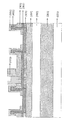
括弧の間の数字は、本発明の工学基板とIII族窒化物装置を、夫々、概略的に図示する図1と図2を参照している。 The numbers between the parentheses refer to FIGS. 1 and 2, which schematically illustrate the engineering substrate and III-nitride device of the present invention, respectively.
本発明の異なる態様の実施形態において、用語「基板」は、装置、回路又はエピタキシャル層が上に形成されて使用されるように下方に位置するなんらかの材料を含む。他の代りの実施形態において、この「基板」は、例えば、ドープトシリコン、ひ化ガリウム(GaAs)、ひ化りん化ガリウム(GaAsP)、りん化インジウム(InP)、ゲルマニウム(Ge)、シリコンゲルマニウム(SiGe)の基板等の半導体基板を含む。「基板」は、例えば、半導体基板部分の他に、SiO2層又はSi3N4層等の誘電体層を含む。よって、用語「基板」は、例えば、ガラス層、メタル層等の層が上に形成されるなんらかの他の基部であり得る。 In an embodiment of a different aspect of the present invention, the term “substrate” includes any material located below such that a device, circuit, or epitaxial layer is formed and used. In other alternative embodiments, the “substrate” may be, for example, doped silicon, gallium arsenide (GaAs), gallium arsenide phosphide (GaAsP), indium phosphide (InP), germanium (Ge), silicon germanium. Including a semiconductor substrate such as a (SiGe) substrate. The “substrate” includes, for example, a dielectric layer such as a SiO 2 layer or a Si 3 N 4 layer in addition to a semiconductor substrate portion. Thus, the term “substrate” can be any other base on which a layer, such as a glass layer, metal layer, etc., is formed.
好ましくは、基板は、シリコン、炭化シリコン、サファイア又はGaN等のIII族窒化物材料からなる。より好ましくは、基板はシリコンからなる。より好ましくは、基板は、(111)又は同等の結晶配列を有する単結晶シリコンからなる。本発明の特定の実施形態において、基板は、(111)結晶配列と150mm、200mm又は300mmの直径を有するシリコンウエハである。好都合に、シリコンウエハを使用することは、シリコンをベースとするCMOSとの共同集積化(co-integration)を可能にする。 Preferably, the substrate is made of a group III nitride material such as silicon, silicon carbide, sapphire or GaN. More preferably, the substrate is made of silicon. More preferably, the substrate comprises (111) or single crystal silicon having an equivalent crystal arrangement. In certain embodiments of the invention, the substrate is a silicon wafer having a (111) crystal array and a diameter of 150 mm, 200 mm or 300 mm. Advantageously, the use of a silicon wafer allows co-integration with silicon-based CMOS.
以下に「III族窒化物層のスタック」と呼ぶ各層がIII族窒化物材料からなる層のスタックは、好ましくは、基板上のエピタキシャル法によって形成される。III族窒化物層のスタックは、一般に、HEMT装置の活性層とも呼ばれるバッファ層201、チャネル層202とバリア層203を備える。別のやり方として、チャネル層は、厚いバッファ層201の上部(頂部)であり得る。活性層の各々は、多層又は傾斜組成を有する層であり得る。
A stack of layers, each of which is hereinafter referred to as a “stack of group III nitride layers”, each layer comprising a group III nitride material, is preferably formed by epitaxial methods on the substrate. A stack of III-nitride layers generally comprises a
HEMTの活性層は、有機金属化学気相成長(MOCVD)又は装置層が真空中の分子堆積によって作り上げられる分子線エピタキシー(MBE)によって製作され得る。 The active layer of the HEMT can be fabricated by metal organic chemical vapor deposition (MOCVD) or molecular beam epitaxy (MBE) where the device layer is built up by molecular deposition in vacuum.
例えば、AlGaAs/GaAs・HEMTである従来のHEMTは、チャネル層(例えば、GaAs)に非ドープトで相対的に低いバンドギャップ材料を使用し、チャネル層は、チャネルと、相対的に高いバンドギャップ材料(例えば、AlGaAs)からなるバリア層内のゲート接点との間に位置するドーピング層によって電子を供給される。異なるバンドギャップを有する材料、即ち、より高いバンドギャップを有する材料とより低いバンドギャップを有する材料を組合せることによって、量子井戸が、組合された材料の間の界面に形成される。電子散乱が高いチャネルドーパント層をチャネル自身と分離することは、チャネル内の電子の移動度を大幅に増大させる。高周波操作における従来のMESFETに対するHEMT技術の基本的な利点を与えるのは、キャリアの高移動度である。AlGaN/GaN・HEMTのより特別な場合、その例ではAlGaNであるより高いバンドギャップ材料は、ドーピングされず、量子井戸中の高いシートキャリア濃度が、圧電分極と自発分極の効果によって得られる。 For example, a conventional HEMT, which is an AlGaAs / GaAs.HEMT, uses an undoped, relatively low bandgap material for the channel layer (eg, GaAs), the channel layer includes a channel and a relatively high bandgap material. Electrons are supplied by a doping layer located between the gate contact in the barrier layer (eg AlGaAs). By combining materials with different band gaps, that is, materials with higher and lower band gaps, quantum wells are formed at the interface between the combined materials. Separating the channel dopant layer with high electron scattering from the channel itself greatly increases the mobility of electrons in the channel. It is the high carrier mobility that gives the fundamental advantage of HEMT technology over conventional MESFETs in high frequency operation. In the more special case of AlGaN / GaN HEMT, the higher bandgap material, which in this example is AlGaN, is not doped and a high sheet carrier concentration in the quantum well is obtained due to the effects of piezoelectric polarization and spontaneous polarization.
HEMTの成長は、典型的に、高品質装置を達成するために、バッファ層201で始まる。基板材料が活性材料と異なる場合、このバッファ層は、又、格子定数の相違に適合する。
HEMT growth typically begins with a
本開示において、バッファ層201の厚さは、例えば、200nmと10μmの間、好ましくは、1μmと3μmの間である。選択肢として、例えば、核形成層である追加バッファ層201’及び/又は例えば、AlGaN、AlN又はGaN中間層等の中間層を、熱膨張と基板と活性層の間の格子ミスマッチを解消するために設けてもよい。
In the present disclosure, the thickness of the
次に、チャネル層202は、GaN、GaAs又はInGaAsからなる。チャネル層の厚さは、例えば、5nmと200nmの間、好ましくは、50nmと200nmの間である。次に、バリア層203は、例えば、AlGaN、AlGaAs又はInAlAsからなる。バリア層の厚さは、例えば、1nmと50nmの間、好ましくは、5nmと30nmの間である。別のやり方として、AlGaAs/GaAsトランジスタを、明示のチャネル層無しに製作することができる。その上、III族窒化物材料からなるキャップ層204(不図示)を、エピタキシャル成長によってバリア層203の上に形成することができる。このような追加キャップ層は、GaNからなると共に、1nmと10nmの間の厚さを有する。
Next, the
次のステップで、窒化シリコンからなる第1パッシベーション層301が、層のスタックの上方層に対して上に位置するとともに当接するように、好ましくは、現場で成長させられる。上方層は、バリア層203、又は追加キャップ層204、又はHEMTを形成するように使用されるIII族窒化物層のスタック(I)のなんらかの他のIII族窒化物層部分であり得る。第1パッシベーション層301は、好ましくは、現場で、即ち、同じプロセスチャンバー内で、MOCVD又はMBE又は同等の手法によって層のスタックに堆積される。特定の実施形態において、第1パッシベーション層301は、現場で900℃と1250℃の間の温度で、より好ましくは、1100℃でMOCVDによって層のスタックに堆積される。
In the next step, a
本発明の異なる態様の実施形態において、第1パッシベーション層は、窒化シリコン(Si3N4)からなる。いくつかの実施形態では、第1パッシベーション層は、更に、Alを含んでもよい。選択肢として、第1パッシベーション層は、均質組成の単一層、又は傾斜組成を有する単一層からなり、又は、それは、複数の層からなる。より好ましくは、第1パッシベーション層は、窒化シリコン(Si3N4)からなる。好ましくは、第1パッシベーション層(現場窒化シリコン)の厚さは、0.5nmと20nmの間、より好ましくは、0.5nmと10nmの間である。 In an embodiment of a different aspect of the present invention, the first passivation layer is made of silicon nitride (Si 3 N 4 ). In some embodiments, the first passivation layer may further include Al. As an option, the first passivation layer consists of a single layer of homogeneous composition or a single layer with a graded composition, or it consists of a plurality of layers. More preferably, the first passivation layer is made of silicon nitride (Si 3 N 4 ). Preferably, the thickness of the first passivation layer (in situ silicon nitride) is between 0.5 nm and 20 nm, more preferably between 0.5 nm and 10 nm.
次に、第1パッシベーション層に対して上に位置すると共に当接する誘電体層302は、原子層堆積(ALD)又はMOCVDによって堆積される。別のやり方として、メタライゼーション(例えば、Alメタライゼーション)を最初に行い、次に、高温酸化を行って、誘電体層を形成する。好ましくは、誘電体層は、ALDによって堆積される。
Next, the
選択肢として、本発明の異なる態様の実施形態において、第1パッシベーション層301、誘電体層302と第2パッシベーション層303は、全て、(真空破壊無しに)現場でMOCVDによって、順にIII族窒化物層の頂部上に成長させられる。
As an option, in embodiments of different aspects of the present invention, the
選択肢として、第1パッシベーション層301と第2パッシベーション層303の各々は、Si3N4からなり、好ましくは、両パッシベーション層は、Si3N4からなる。誘電体層302は、好ましくは、Alからなる。好ましくは、誘電体層302は、AlN、AlSiN、Al2O3及びその組合せ又は混合物からなる群から選択される。より好ましくは、誘電体層302は、AlNからなり、これは、上記方法のステップc)、d)とe)を現場でMOCVDによって行う時に特に好都合である。別のやり方として又は好ましくは、誘電体層302はAl2O3からなる。
As an option, each of the
別のやり方として、誘電体層302は、Al2O3、HfO2、ZrO2又はその組合せ及び/又は混合物等の高k誘電体材料からなる。
Alternatively, the
本発明の異なる態様の実施形態において、誘電体層302は、均質組成を有する単一層であり得る。別のやり方として、絶縁層は、傾斜組成を有する単一層であり得るし、又は、それは複数の層からなる。
In embodiments of the different aspects of the present invention, the
誘電体層302と第1パッシベーション層301は、共に、ゲート誘電体として機能する。従って、現開示の文脈において、ゲート誘電体は、2層ゲート誘電体とも呼ばれる。その上、本発明の方法では、誘電体層302は、LPCVD(又は同等の)窒化シリコンからなる第2パッシベーション層303を選択的にエッチングするためのエッチストップ層として機能する。更に、誘電体層302がAl2O3からなる特定の実施形態においては、それが、第1パッシベーション層301(現場窒化シリコン)に対して湿式エッチングにより選択的に除去される。
Both the
好ましくは、誘電体層は、1nmと30nmの間の、より好ましくは、1nmと20nmの間の厚さを有する。1nmは、エッチストップ層として機能するのに原則的に十分であるので、誘電体層の厚さは、HEMT装置のゲート誘電体仕様によって決定される。 Preferably the dielectric layer has a thickness between 1 nm and 30 nm, more preferably between 1 nm and 20 nm. Since 1 nm is in principle sufficient to function as an etch stop layer, the thickness of the dielectric layer is determined by the gate dielectric specification of the HEMT device.
特定の実施形態において、誘電体層は、ALDによって約400℃の温度で堆積されたAl2O3からなる。選択肢として、高k材料の結晶化温度より低い温度のポスト堆積アニールが適用される。 In certain embodiments, the dielectric layer consists of Al 2 O 3 deposited by ALD at a temperature of about 400 ° C. As an option, a post deposition anneal at a temperature below the crystallization temperature of the high-k material is applied.
一般に、界面準位密度(DIT)は、高温(600−800℃)でポスト堆積アニール(PDA)又はポストメタル堆積アニール(PMA)を適用することによって下げることができる。 In general, the interface state density (DIT) can be lowered by applying a post deposition anneal (PDA) or a post metal deposition anneal (PMA) at a high temperature (600-800 ° C.).
Al2O3からなる誘電体層の特定の場合、600℃と1000℃の間の温度のポスト堆積アニールが適用される。ALD・Al2O3の結晶化温度は、800℃と850℃の間である。PDA又はPMAアニール温度は、多結晶フィルムが好ましい時にこの温度よりも高い。 In the specific case of a dielectric layer made of Al 2 O 3, a post deposition anneal at a temperature between 600 ° C. and 1000 ° C. is applied. The crystallization temperature of ALD • Al 2 O 3 is between 800 ° C. and 850 ° C. The PDA or PMA annealing temperature is higher than this temperature when a polycrystalline film is preferred.
次に、誘電体層302に対して上に位置すると共に当接する窒化シリコン(Si3N4)からなる第2パッシベーション層303が、形成される。第2パッシベーション層303が、LPCVD(バッチ又は単一ウエハプロセス)又はMOCVD又は同等の手法によって450℃より高い温度、より好ましくは550℃より高い温度、更に好ましくは700℃より高い温度で堆積される。
Next, a
本発明の実施形態において、第2パッシベーション層は、オーミック接触合金温度より高い温度で堆積される。オーミック接触合金温度は、金不使用オーミック接触には500℃と700℃の間で、金含有メタライゼーション法では700℃と900℃の間である。 In an embodiment of the invention, the second passivation layer is deposited at a temperature above the ohmic contact alloy temperature. The ohmic contact alloy temperature is between 500 ° C. and 700 ° C. for gold-free ohmic contact and between 700 ° C. and 900 ° C. for gold-containing metallization methods.
好ましくは、第2パッシベーション層は、窒化シリコン(Si3N4)からなる。本開示を通して、LPVCD(バッチ又は単一ウエハプロセス、即ち、SINgen(商標))又はMOCVD又はなんらかの同等の手法によって450℃より高い温度で堆積される窒化シリコンは、「LPCVD窒化シリコン」と呼ばれる。好ましくは、LPCVD窒化シリコンは、550℃と800℃の間、より好ましくは600℃と800℃の間の温度で堆積される。 Preferably, the second passivation layer is made of silicon nitride (Si 3 N 4 ). Throughout this disclosure, silicon nitride deposited at temperatures above 450 ° C. by LPVCD (batch or single wafer process, ie SINgen ™) or MOCVD or any equivalent technique is referred to as “LPCVD silicon nitride”. Preferably, LPCVD silicon nitride is deposited at a temperature between 550 ° C and 800 ° C, more preferably between 600 ° C and 800 ° C.
メタルゲート601材料が、第2パッシベーション層303でストップするように乾式エッチングされる集積法を取扱う実施形態では、第2パッシベーション層303は、メタルゲート・オーバエッチに耐えるのに十分に厚くなければならない。好ましくは、第2パッシベーション層(LPCVD窒化シリコン)は、少なくとも50nm、より好ましくは、約120nmの厚さを有する。
In embodiments dealing with integration methods where the
好都合に、高温で堆積されるLPCVD窒化シリコン層は、プラズマ増強化学気相成長(PECVD)窒化シリコンより優れたパッシベーション層である。LPCVD窒化物は、PECVD窒化物の10−40%よりも低い約3−8%の水素含量を有する。又、LPCVD窒化物は、PECVD窒化物の2.3−3.1g/cm3よりも高い約2.9−3.1g/cm3の密度と、より低いピンホール密度を有する。LPCVD窒化シリコンの同様の値は、MOCVD窒化シリコンの水素含量と密度の値に当てはまる。 Advantageously, the LPCVD silicon nitride layer deposited at high temperature is a better passivation layer than plasma enhanced chemical vapor deposition (PECVD) silicon nitride. LPCVD nitride has a hydrogen content of about 3-8%, which is lower than 10-40% of PECVD nitride. LPCVD nitride also has a density of about 2.9-3.1 g / cm 3 higher than 2.3-3.1 g / cm 3 of PECVD nitride and a lower pinhole density. Similar values for LPCVD silicon nitride apply to the hydrogen content and density values of MOCVD silicon nitride.
PECVD窒化シリコン層は、約300−400℃の温度で堆積されることが知られている。後のステップでより高い温度、例えば、オーミック合金形成の温度を受ける時、このような装置は、ブリスターとクラック又は装置収量を落とす離層を示す。LPCVD窒化シリコンは、このような欠点を有しない。 The PECVD silicon nitride layer is known to be deposited at a temperature of about 300-400 ° C. When subjected to higher temperatures in later steps, such as the temperature of ohmic alloy formation, such devices exhibit blisters and cracks or delamination that reduces device yield. LPCVD silicon nitride does not have such disadvantages.
本発明の方法では、LPCVD窒化シリコンからなる第2パッシベーション層は、下に位置する層を保護して、乾式エッチングプロセス、例えば、オーミック接触形成のためのメタルエッチ及び/又はゲート電極形成のためのメタルゲートエッチ中の2DEG損傷を防止する。LPCVD窒化シリコンのかなり厚い層が、コスト効率のよい、Si−CMOSコンパチブルなプロセスで堆積される。 In the method of the present invention, the second passivation layer made of LPCVD silicon nitride protects the underlying layer and provides a dry etching process, eg, metal etch for ohmic contact formation and / or gate electrode formation. Prevent 2DEG damage during metal gate etch. A fairly thick layer of LPCVD silicon nitride is deposited in a cost-effective, Si-CMOS compatible process.
次のステップで、ソースドレイン・オーミック接触が、HEMT構造上に以下の順、
a)第2パッシベーション層303、誘電体層302と第1パッシベーション層301を選択的にエッチングすることによって、ソースドレイン・オーミック接触領域をパターニングするステップと、
b)メタル層401を堆積及びパターニングすると共に、オーミック合金形成のために熱処理することによって、オーミック接触を形成するステップと
で形成される。
In the next step, the source-drain ohmic contact is in the following order on the HEMT structure:
a) patterning the source / drain ohmic contact region by selectively etching the
b) depositing and patterning the metal layer 401 and heat-treating it to form an ohmic alloy, thereby forming an ohmic contact.
特定の実施形態において、第2パッシベーション層303(LPCVD窒化シリコン)を、Al2O3からなる誘電体層302に向けて選択的にエッチングすることは、SF6からなるプラズマで乾式エッチングによって行われる。次に、Al2O3膜が、稀薄HF溶液の湿式エッチングによって、第1パッシベーション層301(現場Si3N4)に向けて高選択性で除去される。次に、現場窒化シリコン301が、SF6からなるプラズマの乾式エッチングによって、AlGaNバリア層203に向けて高選択性で除去される。
In a specific embodiment, selectively etching the second passivation layer 303 (LPCVD silicon nitride) toward the
メタル層401は、複数のメタル層を備えるメタルスタック、好ましくは、シリコン処理とコンパチブルな金不使用メタルスタックであり得る。ソースドレイン接触を形成するのに使用できる適当なメタル層スタックの例は、Ti/Al、Ti/Ta/Al、Ti/Al/TiW、Ti/Al/TiN、Ti/Al/WとTi/Al/WSiである。他の例は、Ta/Al/M、TaN/Al/M、Ta/Si/M、TaN/Si/Mであり、ここで、Mは、別のメタルスタックであり得る。メタルスタックMの機能は、下に位置する材料の酸化を防止し、及び/又は、ソースドレイン接触の接触抵抗を下げることである。Mは、例えば、TaN/Cuであり得る。 The metal layer 401 may be a metal stack comprising a plurality of metal layers, preferably a gold-free metal stack compatible with silicon processing. Examples of suitable metal layer stacks that can be used to form source drain contacts are Ti / Al, Ti / Ta / Al, Ti / Al / TiW, Ti / Al / TiN, Ti / Al / W and Ti / Al. / WSi. Other examples are Ta / Al / M, TaN / Al / M, Ta / Si / M, TaN / Si / M, where M can be another metal stack. The function of the metal stack M is to prevent oxidation of the underlying material and / or lower the contact resistance of the source / drain contact. M can be, for example, TaN / Cu.
オーミック接触を形成するためのメタル層401のパターニングは、リフトオフ技術又は直接エッチング(例えば、乾式エッチング)によって行うことができる。 The patterning of the metal layer 401 to form the ohmic contact can be performed by a lift-off technique or direct etching (for example, dry etching).
好ましくは、オーミック合金形成のための熱処理は、500℃と900℃の間の温度で行われる。より好ましくは、オーミック合金形成は、600℃と800℃の間のLPCVD窒化物堆積温度より低い温度で行われる。AlGaN/GaNに対する金不使用オーミック接触は、600℃付近の典型的なオーミック合金温度を有するが、金含有オーミック接触の場合、これは800℃付近である。より好ましくは、オーミック合金形成は、Al2O3が誘電体層として使用される特定の実施形態において500℃と850℃の間にある、ゲート誘電体として使用される高k材料の結晶化温度より低い温度で行われる。 Preferably, the heat treatment for forming the ohmic alloy is performed at a temperature between 500 ° C and 900 ° C. More preferably, the ohmic alloy formation is performed at a temperature below the LPCVD nitride deposition temperature between 600 ° C and 800 ° C. Gold-free ohmic contacts to AlGaN / GaN have a typical ohmic alloy temperature around 600 ° C., but for gold-containing ohmic contacts this is around 800 ° C. More preferably, the ohmic alloy formation is the crystallization temperature of the high-k material used as the gate dielectric, which is between 500 ° C. and 850 ° C. in certain embodiments where Al 2 O 3 is used as the dielectric layer. Performed at lower temperatures.
本発明の方法の利点は、オーミック合金形成の後、製造プロセスが、低い熱経費を有する、即ち、オーミック合金形成の温度より高い温度のプロセスステップを含まないことである。 An advantage of the method of the present invention is that after the ohmic alloy formation, the manufacturing process has a low thermal cost, i.e. does not include process steps at a temperature higher than that of the ohmic alloy formation.
次に、ゲート電極601を形成することが、
a)第2パッシベーション層303を誘電体層302に向けて選択的にエッチングすることによって、ゲートトレンチをパターニングするステップと、
b)メタルゲート層を堆積及びパターニングすることによって、少なくともゲートトレンチにおいてゲート電極601を形成するステップと
を更に備える。
Next, forming the
a) patterning the gate trench by selectively etching the
b) forming a
別のやり方として、ゲート電極の形成を第1に行い、次に、オーミック接触を形成することができる。 Alternatively, the gate electrode can be formed first and then an ohmic contact can be formed.
メタルゲート層は、均質組成の層又は傾斜組成の層であり得る。別のやり方として、メタルゲート層は、ゲート電極を形成するのに適した仕事機能を有する多層(又はメタル層のスタック)であり得る。 The metal gate layer may be a homogeneous composition layer or a gradient composition layer. Alternatively, the metal gate layer can be a multilayer (or stack of metal layers) having a work function suitable for forming a gate electrode.
ゲート電極を形成するのに使用できる適当なメタルゲートスタックの例は、ゲートメタル抵抗を下げるために、最終的にAl、Ti/Al、TiN/Al又はTi/TiN/Alの上層と組合されるNi、Mo、TiN、TaN、W、WSiN又はWNである。 Examples of suitable metal gate stacks that can be used to form gate electrodes are ultimately combined with Al, Ti / Al, TiN / Al or Ti / TiN / Al top layers to reduce gate metal resistance. Ni, Mo, TiN, TaN, W, WSiN or WN.
メタルゲート層のパターニングは、リフトオフ技術又は第2パッシベーション層上でストップするメタルゲート層の直接エッチング(例えば、乾式エッチング)によって行うことができる。乾式エッチングを用いる実施形態において、第2パッシベーション層303は、図2に示すように乾式エッチングプロセスのオーバエッチ・ステップ中に、部分的に消費(除去)される。その結果、第2パッシベーション層は、例えば、メタルゲート電極601によって覆われた領域内の元の(アズデポ(堆積時状態)の)厚さと比較すると、露出領域(ゲート縁部とソース/ドレイン接点の間)においてより薄くなっている。
The patterning of the metal gate layer can be performed by lift-off technology or direct etching (eg, dry etching) of the metal gate layer that stops on the second passivation layer. In embodiments using dry etching, the
本発明の方法は、ソースドレイン・オーミック接触とゲート電極のどちらが最初に形成されるかに応じて、誘電体キャップ層501をソースドレイン・オーミック接触又はゲート電極に形成して、後のメタル層401の堆積又はメタルゲート層601の堆積中の、夫々の、ソースドレイン・オーミック接触又はゲート電極を保護するステップを更に備える。
The method of the present invention forms a dielectric cap layer 501 on the source / drain / ohmic contact or gate electrode, depending on whether the source / drain / ohmic contact or the gate electrode is formed first, and the subsequent metal layer 401. And protecting each source / drain ohmic contact or gate electrode during the deposition of the
本発明の別の実施形態では、ゲートトレンチを形成することが、誘電体層302を少なくとも部分的にエッチングするステップと、ゲート電極を形成する前に第2誘電体層302’(不図示)を再堆積するステップとを更に備える。
In another embodiment of the present invention, forming a gate trench includes at least partially etching the
本発明の実施形態において、誘電体層302は、下に位置する第1パッシベーション層301上でストップして、部分的に又は全体的にエッチングされ得る。その後、第2誘電体層302’を、部分的エッチングにより残った誘電体層の上に、又は、誘電体層302が完全に除去された時は第1パッシベーション層301の上に堆積することができる。第2誘電体層302’は、均質組成の層、又は傾斜組成の層又は複数層(多層)のスタックであり得る。第2絶縁層は、ALD、MBE又はスパッタリングによって堆積し、更に、選択肢として、スパッタリングの後にポスト堆積アニールを行うことができる。オーミック接触が第1に形成される実施形態では、第2誘電体層のポスト堆積アニールの温度を、オーミック合金形成温度より低く保つべきである。又、第2誘電体層のポスト堆積アニールの温度は、オーミック接触合金温度以下である。
In an embodiment of the present invention, the
第2の態様において、本発明は、III族窒化物HEMT製作用の工学基板であって、
a)基板101と、
b)基板上で各層がIII族窒化物材料からなる層のスタック(I)(「III族窒化物層のスタック」とも呼ぶ)と、
c)窒化シリコンからなり、III族窒化物層のスタックの上方層に対して上に位置すると共に当接する第1パッシベーション層301と、
d)高k誘電体材料からなり、第1パッシベーション層301に対して上に位置すると共に当接する誘電体層302と、
e)窒化シリコンからなり、誘電体層に対して上に位置すると共に当接する第2パッシベーション層303と
を備える工学基板を開示する。
In a second aspect, the present invention is an engineering substrate of the Group III nitride HEMT operation,
a) a
b) a stack of layers (I) (also referred to as “stack of group III nitride layers”) each layer of which is made of a group III nitride material on the substrate;
c) a
d) a
e) Disclosed is an engineering substrate comprising a
本発明の特定の実施形態において、基板は、(111)配列又は同等の配列を有する単結晶シリコンからなるシリコンウエハである。 In a particular embodiment of the invention, the substrate is a silicon wafer made of single crystal silicon having a (111) or equivalent arrangement.
本発明のHEMT装置の工学基板の第1パッシベーション層301と第2パッシベーション層303は、共に、本発明の方法で堆積された窒化シリコン(「LPCVD窒化シリコン」と呼ぶ)、即ち、約3−8%の低水素含量と約2.9−3.1g/cm3の高密度を有する窒化シリコンからなる。
Both the
本発明の工学基板は、本発明の方法で得られると共に、ゲート誘電体を備えて、Si−CMOSコンパチブルな製造プロセスにHEMT装置を形成するのに使用するのに適したパッシベーションされた基板を提供する利点を有する。 The engineered substrate of the present invention provides a passivated substrate obtained with the method of the present invention and comprising a gate dielectric suitable for use in forming HEMT devices in a Si-CMOS compatible manufacturing process. Has the advantage of
III族窒化物HEMTを製造するための出発基板としての工学基板の別の利点は、ゲート誘電体のポスト堆積アニールやパッシベーション層の高温堆積等の高温経費プロセスが、オーミック接触形成の前に行われるので、従来の集積法の全ての後続プロセスに対して課せられるオーミック合金形成の拘束が解消される結果、HEMT装置の総合性能が改善される。 Another advantage of an engineered substrate as a starting substrate for manufacturing a III-nitride HEMT is that high temperature cost processes such as post deposition annealing of gate dielectrics and high temperature deposition of passivation layers are performed prior to ohmic contact formation. Therefore, the overall performance of the HEMT device is improved as a result of eliminating the ohmic alloy formation constraints imposed on all subsequent processes of the conventional integration method.
III族窒化物HEMTを製造するための出発基板としての工学基板の更に別の利点は、現場窒化シリコン301、誘電体層302とLPCVD窒化シリコン303によって形成される3層スタック(II)が、III族窒化物スタック(I)をパッシベーションすると共に、III族窒化物HEMT装置を製造ために金不使用メタライゼーションステップとメタル(又はメタルゲート)層の乾式エッチングを使用する時のオーミック接触形成とゲート電極形成中にIII族窒化物スタック(I)をパッシベーションすると共に保護するのに適していることである。
Yet another advantage of an engineering substrate as a starting substrate for manufacturing a III-nitride HEMT is that a three-layer stack (II) formed by in
III族窒化物HEMTを製造するための出発基板としての工学基板の更に別の利点は、LPCVD窒化物が、オーミック接触形成の温度経費に耐えられることであり、これは、前述したようにPECVD窒化物では得られない。 Yet another advantage of an engineered substrate as a starting substrate for manufacturing a III-nitride HEMT is that LPCVD nitride can withstand the temperature expense of ohmic contact formation, as described above, by PECVD nitridation. It cannot be obtained with things.
第3の態様で、本発明は、本発明の方法で得られて、基板の活性領域上に形成されると共に、ゲート電極とソースドレイン接点を備えるIII族窒化物HEMTであって、
a)基板101と、
b)基板上で各層がIII族窒化物材料からなる層のスタック(I)(「III族窒化物層のスタック」とも呼ぶ)と、
c)ソースドレイン接点の下を除く活性領域の全てにおいて、スタックの上方層203、204に対して上に位置すると共に当接し、更に、窒化シリコンからなる第1パッシベーション層301と、
d)ソースドレイン接点の下を除く活性領域の全てにおいて、第1パッシベーション層301に対して上に位置すると共に当接し、更に、高k誘電体材料からなる誘電体層302、302’と、
e)ゲート電極の下とソースドレイン接点の下を除く活性領域の全てにおいて、誘電体層に対して上に位置すると共に当接し、更に、LPCVD窒化シリコンからなる第2パッシベーション層303と
を更に備えるIII族窒化物HEMTを開示する。
In a third aspect, the present invention is a III-nitride HEMT obtained by the method of the present invention, formed on an active region of a substrate and comprising a gate electrode and a source drain contact,
a) a
b) a stack of layers (I) (also referred to as “stack of group III nitride layers”) each layer of which is made of a group III nitride material on the substrate;
c) In all of the active region except under the source / drain contact, located above and in contact with the
d) In all of the active region except under the source / drain contact, located above and in contact with the
e) In all of the active region except under the gate electrode and under the source / drain contact, further above and in contact with the dielectric layer, and further comprising a
本発明の一般に適用される態様によれば、本発明の方法の実行の結果として、窒化シリコン、好ましくは、Si3N4からなり、III族窒化物層のスタックの上方層に対して上に位置すると共に当接する第1パッシベーション層と、第1パッシベーション層に対して上に位置すると共に当接する誘電体層とが提供されるか得られる。よって、本発明の方法の実行の結果として、第1パッシベーション層と誘電体層を備える又はからなる2層ゲート誘電体が提供されるか得られる。好ましくは、2層ゲート誘電体を得るために、誘電体層は、第1パッシベーション層の頂部に堆積される。特に、有機金属化学気相成長(MOCVD)リアクタ内で高温で現場でIII族窒化物層に堆積される時の窒化シリコンからなる第1パッシベーション層によって、AlGaNのリラクゼーション、クラッキングと表面粗さを減少する高品質パッシベーション層が得られる。それは、又、頂部AlGaN界面における電荷を中和し及び/又は低界面準位密度を有する高品質界面を形成する。堆積後、第1パッシベーション層の厚さは、選択肢として低減される。このような低減のために、当業者には公知の手法を使用してもよい。堆積後、第1パッシベーション層の厚さは、例えば、約100ナノメートルである。厚さの低減後、第1パッシベーション層の厚さは、例えば、せいぜい20ナノメートル、せいぜい10ナノメートル、又はせいぜい5ナノメートル、例えば、約3ナノメートルである。誘電体層は、Si3N4と異なるもの、又は窒化シリコン不使用のものから選択されてもよい。誘電体層は、例えば、Si3N4と比較して、相対的に高い、例えば、約9より高い誘電率及び/又は相対的に高い、例えば、10MV/cmより高い降伏電界を有する。誘電体層は、例えば、原子層堆積(ALD)によって堆積される。 According to a generally applied aspect of the present invention, as a result of carrying out the method of the present invention, the silicon nitride, preferably Si 3 N 4 , is formed above the upper layer of the stack of group III nitride layers. A first passivation layer positioned and abutting and a dielectric layer positioned above and abutting against the first passivation layer are provided or obtained. Thus, as a result of performing the method of the present invention, a two-layer gate dielectric comprising or consisting of a first passivation layer and a dielectric layer is provided or obtained. Preferably, to obtain a two-layer gate dielectric, the dielectric layer is deposited on top of the first passivation layer. In particular, the first passivation layer of silicon nitride reduces the AlGaN relaxation, cracking and surface roughness when deposited on the III-nitride layer in situ at high temperatures in a metal organic chemical vapor deposition (MOCVD) reactor A high quality passivation layer is obtained. It also neutralizes the charge at the top AlGaN interface and / or forms a high quality interface with a low interface state density. After deposition, the thickness of the first passivation layer is reduced as an option. For such reduction, techniques known to those skilled in the art may be used. After deposition, the thickness of the first passivation layer is, for example, about 100 nanometers. After the thickness reduction, the thickness of the first passivation layer is, for example, no more than 20 nanometers, no more than 10 nanometers, or no more than 5 nanometers, for example about 3 nanometers. The dielectric layer may be selected from one different from Si 3 N 4 or one not using silicon nitride. The dielectric layer has a relatively high dielectric constant, for example, greater than about 9, and / or a relatively high breakdown field, for example, greater than 10 MV / cm, for example, as compared to, for example, Si 3 N 4 . The dielectric layer is deposited, for example, by atomic layer deposition (ALD).
本発明の方法と装置のいくつかの利点を説明するために、我々は、Al2O3ゲート誘電体を使用して、2個の型式のAlGaN/GaN・HEMTを製作及び評価した。好ましくは、両HEMTは、金含有プロセスとリフトオフを使用して処理された。HEMT”A”は、厚い現場窒化物のゲートリセスの後で単一ALD・Al2O3ゲート誘電体を堆積する従来の方法を使用する。HEMT”B”は、薄い現場窒化物の後にALD・Al2O3とLPCVD窒化物堆積を第1ステップとして続ける本発明の方法を使用して処理される。 To illustrate some of the advantages of the method and apparatus of the present invention, we fabricated and evaluated two types of AlGaN / GaN HEMTs using Al 2 O 3 gate dielectric. Preferably, both HEMTs were processed using a gold containing process and lift-off. HEMT “A” uses a conventional method of depositing a single ALD • Al 2 O 3 gate dielectric after a thick in situ nitride gate recess. HEMT “B” is processed using the method of the present invention followed by a thin in-situ nitride followed by ALD • Al 2 O 3 and LPCVD nitride deposition as the first step.
HEMT”A”の製作は、順に、
a)AlN核形成層と、それに後続する2.5μm厚さのAlGaNバッファ層、150nm厚さのGaNチャネル層と10nm厚さの35%AlGaNバリア層からなるシリコン(111)基板の頂部に成長するように、AlGaN/GaNエピ層スタックを形成するステップと、
b)120nmの現場窒化シリコンパッシベーションを形成するステップと、
c)コンタクトリソグラフィ、SF6プラズマを用いた120nm現場窒化物の乾式エッチング、Ti/Al/Mo/Auメタルスタックの堆積、リフトオフと合金、好ましくは、合金形成でオーミック領域を画定することによって、オーミック接触を形成するステップと、
d)素子分離のステップと、
e)コンタクトリソグラフィを用いたゲートトレンチエッチングと、後続のSF6プラズマを用いた120nm現場窒化物の乾式エッチングのステップと、
f)HCl/TMAH溶液内のウエハクリーニングと、その直後の10nmのAl2O3膜の堆積及び700℃ポスト堆積アニールのステップと、
g)コンタクトリソグラフィを用いたゲートメタル堆積と、Mo/Auメタルスタックの堆積及びリフトオフのステップと
を備える。
The production of HEMT "A"
a) Grown on top of a silicon (111) substrate consisting of an AlN nucleation layer followed by a 2.5 μm thick AlGaN buffer layer, 150 nm thick GaN channel layer and 10 nm thick 35% AlGaN barrier layer Forming an AlGaN / GaN epilayer stack,
b) forming a 120 nm in situ silicon nitride passivation;
c) ohmic by defining ohmic regions by contact lithography, dry etching of 120 nm in-situ nitride using SF 6 plasma, deposition of Ti / Al / Mo / Au metal stack, lift-off and alloy, preferably alloy formation Forming a contact;
d) an element isolation step;
e) a gate trench etch using contact lithography followed by a 120 nm in situ nitride dry etch step using SF 6 plasma;
f) wafer cleaning in HCl / TMAH solution, followed immediately by deposition of 10 nm Al 2 O 3 film and 700 ° C. post-deposition annealing;
g) gate metal deposition using contact lithography and Mo / Au metal stack deposition and lift-off steps.
HEMT”B”の製作は、順に、
a)AlN核形成層と、それに後続する2.5μm厚さのAlGaNバッファ層、150nm厚さのGaNチャネル層と10nm厚さの25%AlGaNバリア層からなるシリコン(111)基板の頂部に成長するように、AlGaN/GaNエピ層を形成するステップと、
b)5nmの現場窒化シリコンパッシベーションを形成するステップと、
c)HCl/TMAH溶液内のウエハクリーニングと、その直後の10nmのAl2O3膜の堆積及び700℃ポスト堆積アニールのステップと、
d)120nmのLPCVD窒化物の800℃における堆積のステップと、
e)コンタクトリソグラフィ、SF6プラズマを用いた120nmLPCVD窒化物の乾式エッチング、稀釈BHF(緩衝HF)内のAl2O3・ALD膜の湿式エッチングと、SF6プラズマを用いた5nm現場窒化物の乾式エッチング及び後続のTi/Al/Mo/Auメタルスタックの堆積、リフトオフと合金でオーミック領域を画定することによって、オーミック接触を形成するステップと、
f)素子分離のステップと、
g)コンタクトリソグラフィを用いたゲートトレンチエッチングと、後続のSF6プラズマを用いた120nmLPCVD窒化物の乾式エッチングのステップと、
h)コンタクトリソグラフィを用いたゲートメタル堆積と、Mo/Auメタルスタックの堆積及びリフトオフのステップと
を備える。
The production of HEMT "B"
a) Grown on top of a silicon (111) substrate consisting of an AlN nucleation layer followed by a 2.5 μm thick AlGaN buffer layer, a 150 nm thick GaN channel layer and a 10 nm thick 25% AlGaN barrier layer Forming an AlGaN / GaN epilayer, and
b) forming a 5 nm in situ silicon nitride passivation;
c) wafer cleaning in HCl / TMAH solution, followed by steps of 10 nm Al 2 O 3 film deposition and 700 ° C. post-deposition annealing;
d) a step of deposition of 120 nm LPCVD nitride at 800 ° C .;
e) Contact lithography, dry etching of 120 nm LPCVD nitride using SF 6 plasma, wet etching of Al 2 O 3 .ALD film in diluted BHF (buffered HF), and 5 nm in situ nitride dry using SF 6 plasma Forming an ohmic contact by etching and subsequent deposition of a Ti / Al / Mo / Au metal stack, liftoff and defining an ohmic region with an alloy;
f) an element isolation step;
g) a gate trench etch using contact lithography followed by a dry etch step of 120 nm LPCVD nitride using SF 6 plasma;
h) gate metal deposition using contact lithography and Mo / Au metal stack deposition and lift-off steps.
ステップg)で、10nmのALD・Al2O3膜と5nm現場窒化物層は除去されなかったので、底部の5nm現場窒化物と頂部の10nmAl2O3からなる2層ゲート誘電体が得られた。 In step g), so 10nm ALD · Al 2 O 3 film and 5nm site nitride layer was not removed, two-layer gate dielectric consisting 10nmAl 2 O 3 of 5nm situ nitride and the top of the bottom is obtained It was.
本発明における概念の実行可能性と装置の改善された性能を証明するために、試験が、金含有メタライゼーションとリフトオフで行われた。しかしながら、Si−CMOSコンパチビリティに対しては、金不使用メタライゼーションが望ましい。 To prove the feasibility of the concept in the present invention and the improved performance of the device, tests were conducted with gold-containing metallization and lift-off. However, gold-free metallization is desirable for Si-CMOS compatibility.
HEMT”A”のId−Vdsトランジスタ特性が、HEMT”B”の特性を示す図3(b)と比較して、図3(a)に示されている。Vgsバイアスは、HEMT”A”に対しては10Vから5V(ステップ5V)であり、HEMT”B”に対しては−6Vから2V(ステップ1V)である。HEMT”A”では、AlGaNバリアのAl濃度が高くなるにつれて、Vthがより負になると説明される。HEMT”A”とHEMT”B”の両装置は、良好なピンチオフと低リークの良好なDCトランジスタ挙動を示している。 FIG. 3A shows the Id-Vds transistor characteristics of HEMT “A” compared to FIG. 3B showing the characteristics of HEMT “B”. The Vgs bias is 10V to 5V (step 5V) for HEMT "A" and -6V to 2V (step 1V) for HEMT "B". In HEMT “A”, it is explained that Vth becomes more negative as the Al concentration of the AlGaN barrier increases. Both HEMT “A” and HEMT “B” devices show good DC transistor behavior with good pinch-off and low leakage.
HEMT”A”とHEMT”B”のId−Vgsパルス特性を、夫々、図4(a)と図4(b)に示して、5nm現場窒化物と10nmALD・Al2O3をゲート誘電体として有するHEMT”B”は、10nmALD・Al2O3だけをゲート誘電体として有するHEMT”A”と比較してより高い品質を有する。グラフは、DC挙動(点線)を、休止バイアス点、例えば、HEMT”A”に対するVgs=−10V、Vds=40V休止バイアス点、又、バイアス点、例えば、HEMT”B”に対するVgs=−5V、Vds=50Vバイアス点からのパルス特性(実線)と比較する。従来の方法で処理されたHEMT”A”は、パルス操作下でVthシフトと電流減少を示すが、これは、本発明の方法で処理されたHEMT”B”に当てはまらない。これは、HEMT”A”の低品質なAlGaN/Al2O3界面及び/又はゲート誘電体により、ゲート下のトラッピングが生じていることと関連すると考えられる。 The Id-Vgs pulse characteristics of HEMT “A” and HEMT “B” are shown in FIGS. 4 (a) and 4 (b), respectively, and 5 nm in-situ nitride and 10 nm ALD • Al 2 O 3 are used as gate dielectrics. The HEMT “B” having higher quality than the HEMT “A” having only 10 nm ALD • Al 2 O 3 as a gate dielectric. The graph shows the DC behavior (dotted line) with a pause bias point, eg, Vgs = −10V for HEMT “A”, Vds = 40V pause bias point, and a bias point, eg, Vgs = −5V for HEMT “B”, Compared with the pulse characteristics (solid line) from the Vds = 50 V bias point. The HEMT “A” processed by the conventional method shows a Vth shift and a current decrease under pulse operation, but this is not the case with the HEMT “B” processed by the method of the present invention. This is believed to be related to the under-gate trapping caused by the low quality AlGaN / Al 2 O 3 interface and / or gate dielectric of HEMT “A”.
装置HEMT”A”とHEMT”B”のピンチオフにおける降伏が、夫々、図5(a)と図5(b)で比較される。HEMT”A”では、ゲートトラッピングが、ゲート酸化物降伏により、125Vドレイン電圧で初期の降伏において発生する。HEMT”B”の降伏は400Vに改善される。これは、現場窒化物とALD・Al2O3の組合せを使用する時のゲート誘電体のより優れた品質と関連すると考えられる。 The breakdown at the pinch-off of the devices HEMT “A” and HEMT “B” are compared in FIGS. 5 (a) and 5 (b), respectively. In HEMT “A”, gate trapping occurs in the initial breakdown at 125V drain voltage due to gate oxide breakdown. The yield of HEMT “B” is improved to 400V. This is believed to be related to the superior quality of the gate dielectric when using a combination of in situ nitride and ALD • Al 2 O 3 .
本発明の方法と装置の利点と好ましい利点を更に説明するために、我々は、Al2O3ゲート誘電体を使用して、別の2個の型式のAlGaN/GaN・HEMTを製作及び評価した。両HEMTが、金不使用メタル法、ステッパーリソグラフィと乾式エッチングによるメタルパターニングを用いてCMOSコンパチブルなプロセスによって処理された。HEMT”C”は、厚い現場窒化物のゲートリセスの後に堆積された単一のALD・Al2O3ゲート誘電体で従来の方法を使用する。HEMT”D”は、薄い現場窒化物の堆積と後続のALD・Al2O3及びLPCVD窒化物堆積で本発明の方法を使用して処理される。 To further illustrate the advantages and preferred advantages of the method and apparatus of the present invention, we fabricated and evaluated two other types of AlGaN / GaN HEMTs using Al 2 O 3 gate dielectrics. . Both HEMTs were processed by a CMOS compatible process using gold-free metal method, stepper lithography and metal patterning by dry etching. The HEMT “C” uses conventional methods with a single ALD • Al 2 O 3 gate dielectric deposited after a thick in situ nitride gate recess. HEMT “D” is processed using the method of the present invention with a thin in-situ nitride deposition followed by ALD • Al 2 O 3 and LPCVD nitride deposition.
HEMT”C”の製作は、順に、
a)AlN核形成層と、それに後続する2.5μm厚さのAlGaNバッファ層、150nm厚さのGaNチャネル層と10nm厚さの25%AlGaNバリア層からなるシリコン(111)基板の頂部に成長するように、AlGaN/GaNエピ層スタックを形成するステップと、
b)120nmの現場窒化シリコンパッシベーションを形成するステップと、
c)ステッパーリソグラフィ及びSF6プラズマを用いた120nm現場窒化物の乾式エッチング、Ti/Al/Wメタルスタックの堆積、ステッパーリソグラフィ、乾式メタルエッチングと600℃における合金でオーミック領域を画定することによって、オーミック接触を形成するステップと、
d)PECVD窒化物堆積、ステッパーリソグラフィと現場窒化物に向けたPECVD窒化物の選択的エッチングで、オーミック領域の頂部に誘電体キャップを形成するステップと、
e)素子分離のステップと、
f)ステッパーリソグラフィを用いたゲートトレンチエッチングと、後続のSF6プラズマを用いた120nm現場窒化物の乾式エッチングのステップと、
g)HCl/TMAH溶液内のウエハクリーニングと、その直後の15nmのAl2O3膜の堆積及び600℃ポスト堆積アニールのステップと、
h)W/Ti/Al堆積によるゲートメタル形成、後続のステッパーリソグラフィっと乾式メタルエッチングのステップと
を備える。
The production of HEMT “C”
a) Grown on top of a silicon (111) substrate consisting of an AlN nucleation layer followed by a 2.5 μm thick AlGaN buffer layer, a 150 nm thick GaN channel layer and a 10 nm thick 25% AlGaN barrier layer Forming an AlGaN / GaN epilayer stack,
b) forming a 120 nm in situ silicon nitride passivation;
c) Ohmic by defining ohmic region with stepper lithography and dry etching of 120 nm in situ nitride using SF 6 plasma, deposition of Ti / Al / W metal stack, stepper lithography, dry metal etching and alloy at 600 ° C. Forming a contact;
d) forming a dielectric cap on top of the ohmic region with PECVD nitride deposition, stepper lithography and selective etching of PECVD nitride for in situ nitride;
e) an element isolation step;
f) a gate trench etch using stepper lithography followed by a 120 nm in situ nitride dry etch step using SF 6 plasma;
g) wafer cleaning in HCl / TMAH solution, followed by steps of 15 nm Al 2 O 3 film deposition and 600 ° C. post-deposition annealing;
h) gate metal formation by W / Ti / Al deposition, followed by stepper lithography and dry metal etching steps.
HEMT”D”の製作は、順に、
a)AlN核形成層と、それに後続する2.5μm厚さのAlGaNバッファ層、150nm厚さのGaNチャネル層と10nm厚さの25%AlGaNバリア層からなるシリコン(111)基板の頂部に成長するように、AlGaN/GaNエピ層を形成するステップと、
b)10nmの現場窒化シリコンパッシベーションを形成するステップと、
c)HCl/TMAH溶液内のウエハクリーニングと、その直後の5nmのAl2O3膜の堆積及び700℃ポスト堆積アニールのステップと、
d)120nmのLPCVD窒化物の800℃における堆積のステップと、
e)ステッパーリソグラフィ、SF6プラズマを用いた120nmLPCVD窒化物の乾式エッチング、1%HF内のAl2O3・ALD膜の湿式エッチングとSF6プラズマを用いた5nm現場窒化物の乾式エッチングでオーミック領域を画定することによって、オーミック接触を形成するステップと、
f)PECVD窒化物堆積、ステッパーリソグラフィとLPCVD窒化物に向けたPECVD窒化物の選択的エッチングで、オーミック領域の頂部に誘電体キャップを形成するステップと、
g)素子分離のステップと、
h)コンタクトリソグラフィを用いたゲートトレンチエッチングと、後続のSF6プラズマを用いた120nmLPCVD窒化物の乾式エッチングのステップと
を備える。
The production of HEMT “D”
a) Grown on top of a silicon (111) substrate consisting of an AlN nucleation layer followed by a 2.5 μm thick AlGaN buffer layer, a 150 nm thick GaN channel layer and a 10 nm thick 25% AlGaN barrier layer Forming an AlGaN / GaN epilayer, and
b) forming a 10 nm in situ silicon nitride passivation;
c) cleaning the wafer in HCl / TMAH solution, followed by steps of 5 nm Al 2 O 3 film deposition and 700 ° C. post-deposition annealing immediately after;
d) a step of deposition of 120 nm LPCVD nitride at 800 ° C .;
e) Ohmic region with stepper lithography, dry etching of 120 nm LPCVD nitride using SF 6 plasma, wet etching of Al 2 O 3 .ALD film in 1% HF and 5 nm in situ nitride dry etching using SF 6 plasma Forming an ohmic contact by defining
f) forming a dielectric cap on top of the ohmic region with PECVD nitride deposition, selective etching of PECVD nitride for stepper lithography and LPCVD nitride;
g) an element isolation step;
h) gate trench etching using contact lithography, followed by a step of dry etching of 120 nm LPCVD nitride using SF 6 plasma.
Ti/Al/Wメタルスタックの堆積、ステッパーリソグラフィ、乾式メタルエッチングと600℃の合金が、ステップe)に続く。又、5nmALD・Al2O3と10nm現場窒化物層は除去されなかったので、底部の10nm現場窒化物と頂部の5nmAl2O3からなる2層ゲート誘電体が形成される。 Ti / Al / W metal stack deposition, stepper lithography, dry metal etching and 600 ° C. alloy follow step e). Also, since the 5 nm ALD • Al 2 O 3 and 10 nm in situ nitride layers were not removed, a two layer gate dielectric consisting of the bottom 10 nm in situ nitride and the top 5 nm Al 2 O 3 is formed.
HEMT”D”とHEMT”C”のId−Vgs特性Ig−Vgs特性を図6に示して、10nm現場窒化物と5nmALD・Al2O3をゲート誘電体として有するHEMT”D”は、15nmALD・Al2O3だけをゲート誘電体として有するHEMT”C”と比較してより高い品質を有する。HEMT”D”では、前方ゲートバイアスゲートリーク電流Igは、約2桁低い。 The Id-Vgs characteristics of the HEMT “D” and the HEMT “C” are shown in FIG. 6. The HEMT “D” having 10 nm in-situ nitride and 5 nm ALD • Al 2 O 3 as the gate dielectric is shown in FIG. It has a higher quality compared to HEMT “C” with only Al 2 O 3 as the gate dielectric. In HEMT “D”, the forward gate bias gate leakage current Ig is about two orders of magnitude lower.
HEMT”C”とHEMT”D”の全150mmウエハに対するピンチオフにおける降伏の分布が、図7に示されている。HEMT”D”のゲート誘電体のより優れた品質が、一様な高降伏電圧を生じる。HEMT”D”の平均降伏電圧は800Vであるのに対し、HEMT”C”のそれは200Vである。HEMT”D”の典型的なId−Vds(Vgs=−8V)降伏曲線が、図8に示される。ドレインリークは、Vdsが約700Vまで1μA/mmより低い。 The distribution of yield at pinch-off for all 150 mm wafers of HEMT “C” and HEMT “D” is shown in FIG. The superior quality of the HEMT “D” gate dielectric results in a uniform high breakdown voltage. The average breakdown voltage of HEMT “D” is 800V, while that of HEMT “C” is 200V. A typical Id-Vds (Vgs = -8V) yield curve for HEMT "D" is shown in FIG. The drain leakage is lower than 1 μA / mm until Vds is about 700V.
図9は、HEMT”D”の分散挙動を示す。そのグラフは、(Vds=0V、Vgs=0V)と(Vds=50V、Vgs=−5V)の休止バイアス点からパルシングする時のId−Vds曲線を比較する。観察された電流コラプスは、非常に限定的である。 FIG. 9 shows the dispersion behavior of HEMT “D”. The graph compares the Id-Vds curves when pulsing from rest bias points (Vds = 0V, Vgs = 0V) and (Vds = 50V, Vgs = -5V). The observed current collapse is very limited.
101 基板
201 バッファ層
202 チャネル層
203 バリア層
301 第1パッシベーション層
302 誘電体層
303 第2パッシベーション層
401 メタル層
501 誘電体キャップ層
601 ゲート電極
DESCRIPTION OF
Claims (10)
a)基板(101)を提供するステップと、
b)III族窒化物層のスタック(I)を基板(101)上に形成するステップと、
c)窒化シリコン、好ましくは、Si3N4を含み、スタック(I)の上方層(203、204)に対して上に位置すると共に当接する第1パッシベーション層(301)を形成するステップと、
d)第1パッシベーション層(301)に対して上に位置すると共に当接する誘電体層(302)を形成するステップと、
e)窒化シリコン、好ましくは、Si3N4を含み、誘電体層(302)に対して上に位置すると共に当接する第2パッシベーション層(303)を形成し、第2パッシベーション層(303)が、低圧化学気相成長法及び/又は有機金属化学気相成長法等の化学気相成長法によって450℃より高い温度で堆積されるステップと、
f)第1パッシベーション層(301)と誘電体層(302)の少なくとも一部を含むゲート誘電体が形成されるように、ソースドレイン・オーミック接触とゲート電極(601)を形成するステップと、
を含み、
ゲート電極を形成するステップが、
第2パッシベーション層(303)を誘電体層に向けて選択的にエッチングすることによって、ゲートトレンチをパターニングするステップと、メタルゲート層を堆積及びパターニングすることによって、少なくともゲートトレンチにおいてゲート電極(601)を形成するステップと、を更に含み、
ゲートトレンチを形成するステップが、誘電体層を少なくとも部分的にエッチングするステップと、ゲート電極を形成する前に第2誘電体層を再堆積するステップと、を更に含む方法。 In a method of manufacturing a group III nitride HEMT having a gate electrode and a source / drain ohmic contact,
a) providing a substrate (101);
b) forming a stack of group III nitride layers (I) on the substrate (101);
c) forming a first passivation layer (301) comprising silicon nitride, preferably Si 3 N 4 and located above and abutting against the upper layer (203, 204) of the stack (I);
d) forming a dielectric layer (302) located above and abutting against the first passivation layer (301);
e) forming a second passivation layer (303) comprising silicon nitride, preferably Si 3 N 4 , located above and in contact with the dielectric layer (302), wherein the second passivation layer (303) Depositing at a temperature higher than 450 ° C. by chemical vapor deposition, such as low pressure chemical vapor deposition and / or metalorganic chemical vapor deposition;
f) forming a source drain ohmic contact and a gate electrode (601) such that a gate dielectric comprising at least a portion of the first passivation layer (301) and the dielectric layer (302) is formed;
Only including,
Forming the gate electrode comprises:
Patterning the gate trench by selectively etching the second passivation layer (303) toward the dielectric layer; and depositing and patterning a metal gate layer to at least the gate electrode (601) in the gate trench. Further comprising the step of:
The method of forming the gate trench further comprises at least partially etching the dielectric layer and redepositing the second dielectric layer prior to forming the gate electrode .
第2パッシベーション層(303)、誘電体層(302)及び第1パッシベーション層(301)を選択的にエッチングすることによって、ソースドレイン・オーミック接触領域をパターニングするステップと、
メタル層(401)を堆積及びパターニングすると共に、オーミック合金を形成することによって、オーミック接触を形成するステップと、
を更に備える請求項1乃至3のいずれかに記載の方法。 Forming a source-drain ohmic contact comprising:
Patterning the source-drain ohmic contact region by selectively etching the second passivation layer (303), the dielectric layer (302) and the first passivation layer (301);
Forming an ohmic contact by depositing and patterning a metal layer (401) and forming an ohmic alloy;
The method according to claim 1, further comprising:
Applications Claiming Priority (4)
| Application Number | Priority Date | Filing Date | Title |
|---|---|---|---|
| US201161498951P | 2011-06-20 | 2011-06-20 | |
| US61/498,951 | 2011-06-20 | ||
| US201161526107P | 2011-08-22 | 2011-08-22 | |
| US61/526,107 | 2011-08-22 |
Publications (3)
| Publication Number | Publication Date |
|---|---|
| JP2013012735A JP2013012735A (en) | 2013-01-17 |
| JP2013012735A5 JP2013012735A5 (en) | 2015-05-28 |
| JP6054070B2 true JP6054070B2 (en) | 2016-12-27 |
Family
ID=46419896
Family Applications (1)
| Application Number | Title | Priority Date | Filing Date |
|---|---|---|---|
| JP2012138007A Active JP6054070B2 (en) | 2011-06-20 | 2012-06-19 | CMOS compatible method for manufacturing a HEMT device and the HEMT device |
Country Status (3)
| Country | Link |
|---|---|
| US (2) | US9070758B2 (en) |
| EP (1) | EP2541605A1 (en) |
| JP (1) | JP6054070B2 (en) |
Families Citing this family (55)
| Publication number | Priority date | Publication date | Assignee | Title |
|---|---|---|---|---|
| US7417266B1 (en) | 2004-06-10 | 2008-08-26 | Qspeed Semiconductor Inc. | MOSFET having a JFET embedded as a body diode |
| US8633094B2 (en) | 2011-12-01 | 2014-01-21 | Power Integrations, Inc. | GaN high voltage HFET with passivation plus gate dielectric multilayer structure |
| US8940620B2 (en) | 2011-12-15 | 2015-01-27 | Power Integrations, Inc. | Composite wafer for fabrication of semiconductor devices |
| US9379191B2 (en) * | 2011-12-28 | 2016-06-28 | Taiwan Semiconductor Manufacturing Company, Ltd. | High electron mobility transistor including an isolation region |
| US8963162B2 (en) | 2011-12-28 | 2015-02-24 | Taiwan Semiconductor Manufacturing Company, Ltd. | High electron mobility transistor |
| TWI458092B (en) * | 2012-01-10 | 2014-10-21 | Univ Nat Chiao Tung | A structure of gan high electron mobility transistor |
| KR20130128281A (en) * | 2012-05-16 | 2013-11-26 | 삼성전자주식회사 | High electron mobility transistor and method of manufacturing the same |
| CN102723358B (en) * | 2012-05-30 | 2015-01-07 | 苏州能讯高能半导体有限公司 | Isolated gate field effect transistor and manufacture method thereof |
| US9349902B2 (en) | 2012-06-01 | 2016-05-24 | Taiwan Semiconductor Manufacturing Company, Ltd. | System and method for reducing irregularities on the surface of a backside illuminated photodiode |
| US9111868B2 (en) | 2012-06-26 | 2015-08-18 | Freescale Semiconductor, Inc. | Semiconductor device with selectively etched surface passivation |
| US10522670B2 (en) | 2012-06-26 | 2019-12-31 | Nxp Usa, Inc. | Semiconductor device with selectively etched surface passivation |
| US8946776B2 (en) | 2012-06-26 | 2015-02-03 | Freescale Semiconductor, Inc. | Semiconductor device with selectively etched surface passivation |
| US10825924B2 (en) | 2012-06-26 | 2020-11-03 | Nxp Usa, Inc. | Semiconductor device with selectively etched surface passivation |
| US20140077266A1 (en) * | 2012-09-14 | 2014-03-20 | Power Integrations, Inc. | Heterostructure Transistor with Multiple Gate Dielectric Layers |
| EP2746760B1 (en) * | 2012-12-21 | 2018-02-07 | Stichting IMEC Nederland | 2DEG sensor, method for making such sensor and use of such sensor |
| US8946779B2 (en) | 2013-02-26 | 2015-02-03 | Freescale Semiconductor, Inc. | MISHFET and Schottky device integration |
| US8912573B2 (en) | 2013-02-26 | 2014-12-16 | Taiwan Semiconductor Manufacturing Company, Ltd. | Semiconductor device containing HEMT and MISFET and method of forming the same |
| US8928037B2 (en) * | 2013-02-28 | 2015-01-06 | Power Integrations, Inc. | Heterostructure power transistor with AlSiN passivation layer |
| JP2014187238A (en) * | 2013-03-25 | 2014-10-02 | Toyoda Gosei Co Ltd | Mis semiconductor device manufacturing method |
| US9082722B2 (en) * | 2013-03-25 | 2015-07-14 | Raytheon Company | Monolithic integrated circuit (MMIC) structure and method for forming such structure |
| US8916427B2 (en) * | 2013-05-03 | 2014-12-23 | Texas Instruments Incorporated | FET dielectric reliability enhancement |
| JP6136573B2 (en) * | 2013-05-27 | 2017-05-31 | 富士通株式会社 | Semiconductor device and manufacturing method of semiconductor device |
| KR102193085B1 (en) * | 2013-07-08 | 2020-12-21 | 이피션트 파워 컨버젼 코퍼레이션 | Method to fabricate self-aligned isolation in gallium nitride devices and integrated circuits |
| US9263569B2 (en) * | 2013-08-05 | 2016-02-16 | Taiwan Semiconductor Manufacturing Company, Ltd. | MISFET device and method of forming the same |
| EP2843696A1 (en) * | 2013-08-27 | 2015-03-04 | IMEC vzw | A method for dopant implantation of FinFET structures |
| EP2881982B1 (en) * | 2013-12-05 | 2019-09-04 | IMEC vzw | Method for fabricating cmos compatible contact layers in semiconductor devices |
| EP2930754A1 (en) | 2014-04-11 | 2015-10-14 | Nxp B.V. | Semiconductor device |
| JP6591169B2 (en) * | 2015-02-04 | 2019-10-16 | 株式会社東芝 | Semiconductor device and manufacturing method thereof |
| JP6591168B2 (en) * | 2015-02-04 | 2019-10-16 | 株式会社東芝 | Semiconductor device and manufacturing method thereof |
| JP6520197B2 (en) | 2015-02-20 | 2019-05-29 | 富士通株式会社 | Compound semiconductor device and method of manufacturing the same |
| US9679762B2 (en) * | 2015-03-17 | 2017-06-13 | Toshiba Corporation | Access conductivity enhanced high electron mobility transistor |
| JP6478752B2 (en) * | 2015-03-24 | 2019-03-06 | 株式会社東芝 | Semiconductor device and manufacturing method thereof |
| JP6635400B2 (en) * | 2015-06-30 | 2020-01-22 | サンケン電気株式会社 | Semiconductor device |
| CN105405878B (en) * | 2015-11-27 | 2018-11-16 | 西安电子科技大学 | The insulated gate AlGaN/GaN high electron mobility transistor of more channel side grid structures |
| CN105448962B (en) * | 2015-11-27 | 2019-01-08 | 西安电子科技大学 | The AlGaN/GaN high electron mobility transistor of more channel side grid structures |
| US9917171B2 (en) | 2016-07-21 | 2018-03-13 | International Business Machines Corporation | Low-resistive, CMOS-compatible, Au-free ohmic contact to N—InP |
| CN106601787B (en) * | 2016-12-01 | 2020-06-26 | 北京大学 | InxAlyGa1-x-yN/GaN heterostructure and epitaxial method thereof |
| JP6834709B2 (en) * | 2017-04-03 | 2021-02-24 | 住友電気工業株式会社 | Method for forming a silicon nitride passivation film and method for manufacturing a semiconductor device |
| US11041844B2 (en) * | 2017-09-29 | 2021-06-22 | Palogen, Inc. | Nanopore device and method of manufacturing same |
| CN109659361B (en) | 2017-10-12 | 2022-03-04 | 电力集成公司 | Gate stack for heterojunction devices |
| TWI674630B (en) * | 2018-10-18 | 2019-10-11 | 環球晶圓股份有限公司 | Manufacturing method of high electron mobility transistor |
| US10741494B2 (en) * | 2018-11-07 | 2020-08-11 | Semiconductor Components Industries, Llc | Electronic device including a contact structure contacting a layer |
| CN112242441A (en) * | 2019-07-16 | 2021-01-19 | 联华电子股份有限公司 | High electron mobility transistor |
| CN110600443B (en) * | 2019-08-02 | 2021-07-20 | 中国科学院微电子研究所 | Heterogeneous integrated HEMT device structure |
| CN110660780A (en) * | 2019-09-19 | 2020-01-07 | 大同新成新材料股份有限公司 | Process for forming nitride semiconductor device |
| US20230006053A1 (en) | 2019-11-29 | 2023-01-05 | Nippon Telegraph And Telephone Corporation | Field-Effect Transistor and Method for Manufacturing the Same |
| CN112509924B (en) * | 2020-11-04 | 2022-08-05 | 中国电子科技集团公司第五十五研究所 | Preparation method of E/D integrated GaN HEMT device |
| CN112652535A (en) * | 2020-12-22 | 2021-04-13 | 深圳市美浦森半导体有限公司 | Gallium nitride heterojunction diode preparation method and diode |
| WO2022177504A1 (en) * | 2021-02-22 | 2022-08-25 | Igss-Gan Pte Ltd | Semiconductor apparatus and method for fabricating thereof |
| CN113113478B (en) * | 2021-03-01 | 2022-10-04 | 西安电子科技大学 | GaN-based radio frequency power device based on ohmic regrowth and preparation method thereof |
| CN113035783B (en) * | 2021-03-12 | 2022-07-22 | 浙江集迈科微电子有限公司 | Graphene device and GaN device heterogeneous integrated structure and preparation method thereof |
| CN115132585A (en) * | 2021-03-29 | 2022-09-30 | 联华电子股份有限公司 | High electron mobility transistor and manufacturing method thereof |
| CN115394648A (en) * | 2021-05-25 | 2022-11-25 | 联华电子股份有限公司 | Nitride semiconductor element and method for manufacturing the same |
| CN114023817A (en) * | 2021-11-01 | 2022-02-08 | 桂林理工大学 | GaN HEMT device with piezoelectric layer |
| WO2023127520A1 (en) * | 2021-12-27 | 2023-07-06 | ローム株式会社 | Nitride semiconductor device and manufacturing method therefor |
Family Cites Families (20)
| Publication number | Priority date | Publication date | Assignee | Title |
|---|---|---|---|---|
| TW457555B (en) * | 1998-03-09 | 2001-10-01 | Siemens Ag | Surface passivation using silicon oxynitride |
| JP2002009253A (en) * | 2000-06-19 | 2002-01-11 | Sony Corp | Semiconductor device and its manufacturing method |
| US6593193B2 (en) * | 2001-02-27 | 2003-07-15 | Matsushita Electric Industrial Co., Ltd. | Semiconductor device and method for fabricating the same |
| US7230284B2 (en) * | 2001-07-24 | 2007-06-12 | Cree, Inc. | Insulating gate AlGaN/GaN HEMT |
| US7446217B2 (en) * | 2002-11-14 | 2008-11-04 | Advanced Technology Materials, Inc. | Composition and method for low temperature deposition of silicon-containing films |
| US20070138506A1 (en) * | 2003-11-17 | 2007-06-21 | Braddock Walter D | Nitride metal oxide semiconductor integrated transistor devices |
| EP2273553B1 (en) | 2004-06-30 | 2020-02-12 | IMEC vzw | A method for fabricating AlGaN/GaN HEMT devices |
| JP4845872B2 (en) | 2005-01-25 | 2011-12-28 | 富士通株式会社 | Semiconductor device having MIS structure and manufacturing method thereof |
| US20070018199A1 (en) | 2005-07-20 | 2007-01-25 | Cree, Inc. | Nitride-based transistors and fabrication methods with an etch stop layer |
| JP4823671B2 (en) | 2005-12-13 | 2011-11-24 | 日本電信電話株式会社 | Heterostructure field effect transistor using nitride semiconductor |
| US7709269B2 (en) * | 2006-01-17 | 2010-05-04 | Cree, Inc. | Methods of fabricating transistors including dielectrically-supported gate electrodes |
| US8431962B2 (en) * | 2007-12-07 | 2013-04-30 | Northrop Grumman Systems Corporation | Composite passivation process for nitride FET |
| JP5345328B2 (en) * | 2008-02-22 | 2013-11-20 | 住友電工デバイス・イノベーション株式会社 | Manufacturing method of semiconductor device |
| US8129555B2 (en) * | 2008-08-12 | 2012-03-06 | Air Products And Chemicals, Inc. | Precursors for depositing silicon-containing films and methods for making and using same |
| US8105889B2 (en) | 2009-07-27 | 2012-01-31 | Cree, Inc. | Methods of fabricating transistors including self-aligned gate electrodes and source/drain regions |
| WO2011039800A1 (en) * | 2009-09-29 | 2011-04-07 | 株式会社 東芝 | Semiconductor device |
| US8946776B2 (en) * | 2012-06-26 | 2015-02-03 | Freescale Semiconductor, Inc. | Semiconductor device with selectively etched surface passivation |
| US9111868B2 (en) * | 2012-06-26 | 2015-08-18 | Freescale Semiconductor, Inc. | Semiconductor device with selectively etched surface passivation |
| US8803158B1 (en) * | 2013-02-18 | 2014-08-12 | Taiwan Semiconductor Manufacturing Company, Ltd. | High electron mobility transistor and method of forming the same |
| US8946779B2 (en) * | 2013-02-26 | 2015-02-03 | Freescale Semiconductor, Inc. | MISHFET and Schottky device integration |
-
2012
- 2012-06-18 US US13/525,644 patent/US9070758B2/en active Active
- 2012-06-19 EP EP12172551A patent/EP2541605A1/en not_active Ceased
- 2012-06-19 JP JP2012138007A patent/JP6054070B2/en active Active
-
2015
- 2015-06-26 US US14/752,375 patent/US9252258B2/en active Active
Also Published As
| Publication number | Publication date |
|---|---|
| US20120319169A1 (en) | 2012-12-20 |
| EP2541605A1 (en) | 2013-01-02 |
| US9252258B2 (en) | 2016-02-02 |
| US9070758B2 (en) | 2015-06-30 |
| JP2013012735A (en) | 2013-01-17 |
| US20150295076A1 (en) | 2015-10-15 |
Similar Documents
| Publication | Publication Date | Title |
|---|---|---|
| JP6054070B2 (en) | CMOS compatible method for manufacturing a HEMT device and the HEMT device | |
| JP5785153B2 (en) | Compensated gate MISFET and manufacturing method thereof | |
| JP5823138B2 (en) | Nitride semiconductor devices | |
| Van Hove et al. | CMOS process-compatible high-power low-leakage AlGaN/GaN MISHEMT on silicon | |
| US8604486B2 (en) | Enhancement mode group III-V high electron mobility transistor (HEMT) and method for fabrication | |
| EP2146378B1 (en) | Semiconductor device | |
| JP5809802B2 (en) | Semiconductor device | |
| JP5202312B2 (en) | Group III nitride enhancement type devices | |
| US20140335666A1 (en) | Growth of High-Performance III-Nitride Transistor Passivation Layer for GaN Electronics | |
| KR101092467B1 (en) | Enhancement normally off nitride semiconductor device and manufacturing method thereof | |
| WO2009116283A1 (en) | Semiconductor device and method for manufacturing said device | |
| US10679860B2 (en) | Self-aligning source, drain and gate process for III-V nitride MISHEMTs | |
| US20140252371A1 (en) | Heterojunction transistor and method of fabricating the same | |
| JP2008010803A (en) | Nitride semiconductor field-effect transistor | |
| JP2016174140A (en) | High electron mobility transistor device and method of manufacturing the same | |
| JP5183975B2 (en) | Enhanced mode field effect device and manufacturing method thereof | |
| US8558242B2 (en) | Vertical GaN-based metal insulator semiconductor FET | |
| JP7308593B2 (en) | Nitride semiconductor device | |
| JP2009076673A (en) | Field-effect transistor using group iii nitride semiconductor | |
| JP2002329863A (en) | Semiconductor device and its manufacturing method | |
| JP6472839B2 (en) | Semiconductor device | |
| TW202329461A (en) | High electron mobility transistor and method for fabricating the same | |
| KR20190112523A (en) | Heterostructure Field Effect Transistor and production method thereof | |
| JP5463529B2 (en) | Method for manufacturing field effect transistor | |
| JP2008227432A (en) | Nitride compound semiconductor element and its production process |
Legal Events
| Date | Code | Title | Description |
|---|---|---|---|
| A521 | Request for written amendment filed |
Free format text: JAPANESE INTERMEDIATE CODE: A523 Effective date: 20150410 |
|
| A621 | Written request for application examination |
Free format text: JAPANESE INTERMEDIATE CODE: A621 Effective date: 20150410 |
|
| A977 | Report on retrieval |
Free format text: JAPANESE INTERMEDIATE CODE: A971007 Effective date: 20160219 |
|
| A131 | Notification of reasons for refusal |
Free format text: JAPANESE INTERMEDIATE CODE: A131 Effective date: 20160301 |
|
| A601 | Written request for extension of time |
Free format text: JAPANESE INTERMEDIATE CODE: A601 Effective date: 20160601 |
|
| A601 | Written request for extension of time |
Free format text: JAPANESE INTERMEDIATE CODE: A601 Effective date: 20160722 |
|
| A521 | Request for written amendment filed |
Free format text: JAPANESE INTERMEDIATE CODE: A523 Effective date: 20160830 |
|
| TRDD | Decision of grant or rejection written | ||
| A01 | Written decision to grant a patent or to grant a registration (utility model) |
Free format text: JAPANESE INTERMEDIATE CODE: A01 Effective date: 20161101 |
|
| A61 | First payment of annual fees (during grant procedure) |
Free format text: JAPANESE INTERMEDIATE CODE: A61 Effective date: 20161130 |
|
| R150 | Certificate of patent or registration of utility model |
Ref document number: 6054070 Country of ref document: JP Free format text: JAPANESE INTERMEDIATE CODE: R150 |
|
| R250 | Receipt of annual fees |
Free format text: JAPANESE INTERMEDIATE CODE: R250 |
|
| R250 | Receipt of annual fees |
Free format text: JAPANESE INTERMEDIATE CODE: R250 |
|
| R250 | Receipt of annual fees |
Free format text: JAPANESE INTERMEDIATE CODE: R250 |
|
| R250 | Receipt of annual fees |
Free format text: JAPANESE INTERMEDIATE CODE: R250 |
|
| R250 | Receipt of annual fees |
Free format text: JAPANESE INTERMEDIATE CODE: R250 |