JP6035015B2 - Circuit board - Google Patents
Circuit board Download PDFInfo
- Publication number
- JP6035015B2 JP6035015B2 JP2011196819A JP2011196819A JP6035015B2 JP 6035015 B2 JP6035015 B2 JP 6035015B2 JP 2011196819 A JP2011196819 A JP 2011196819A JP 2011196819 A JP2011196819 A JP 2011196819A JP 6035015 B2 JP6035015 B2 JP 6035015B2
- Authority
- JP
- Japan
- Prior art keywords
- imager
- circuit board
- temperature adjustment
- temperature
- printed circuit
- Prior art date
- Legal status (The legal status is an assumption and is not a legal conclusion. Google has not performed a legal analysis and makes no representation as to the accuracy of the status listed.)
- Active
Links
Images


Classifications
-
- H—ELECTRICITY
- H05—ELECTRIC TECHNIQUES NOT OTHERWISE PROVIDED FOR
- H05K—PRINTED CIRCUITS; CASINGS OR CONSTRUCTIONAL DETAILS OF ELECTRIC APPARATUS; MANUFACTURE OF ASSEMBLAGES OF ELECTRICAL COMPONENTS
- H05K1/00—Printed circuits
- H05K1/02—Details
- H05K1/0201—Thermal arrangements, e.g. for cooling, heating or preventing overheating
-
- H—ELECTRICITY
- H05—ELECTRIC TECHNIQUES NOT OTHERWISE PROVIDED FOR
- H05K—PRINTED CIRCUITS; CASINGS OR CONSTRUCTIONAL DETAILS OF ELECTRIC APPARATUS; MANUFACTURE OF ASSEMBLAGES OF ELECTRICAL COMPONENTS
- H05K2201/00—Indexing scheme relating to printed circuits covered by H05K1/00
- H05K2201/09—Shape and layout
- H05K2201/09009—Substrate related
- H05K2201/09054—Raised area or protrusion of metal substrate
-
- H—ELECTRICITY
- H05—ELECTRIC TECHNIQUES NOT OTHERWISE PROVIDED FOR
- H05K—PRINTED CIRCUITS; CASINGS OR CONSTRUCTIONAL DETAILS OF ELECTRIC APPARATUS; MANUFACTURE OF ASSEMBLAGES OF ELECTRICAL COMPONENTS
- H05K2201/00—Indexing scheme relating to printed circuits covered by H05K1/00
- H05K2201/09—Shape and layout
- H05K2201/09009—Substrate related
- H05K2201/09063—Holes or slots in insulating substrate not used for electrical connections
-
- H—ELECTRICITY
- H05—ELECTRIC TECHNIQUES NOT OTHERWISE PROVIDED FOR
- H05K—PRINTED CIRCUITS; CASINGS OR CONSTRUCTIONAL DETAILS OF ELECTRIC APPARATUS; MANUFACTURE OF ASSEMBLAGES OF ELECTRICAL COMPONENTS
- H05K2201/00—Indexing scheme relating to printed circuits covered by H05K1/00
- H05K2201/09—Shape and layout
- H05K2201/09009—Substrate related
- H05K2201/09072—Hole or recess under component or special relationship between hole and component
-
- H—ELECTRICITY
- H05—ELECTRIC TECHNIQUES NOT OTHERWISE PROVIDED FOR
- H05K—PRINTED CIRCUITS; CASINGS OR CONSTRUCTIONAL DETAILS OF ELECTRIC APPARATUS; MANUFACTURE OF ASSEMBLAGES OF ELECTRICAL COMPONENTS
- H05K2201/00—Indexing scheme relating to printed circuits covered by H05K1/00
- H05K2201/10—Details of components or other objects attached to or integrated in a printed circuit board
- H05K2201/10007—Types of components
- H05K2201/10121—Optical component, e.g. opto-electronic component
-
- H—ELECTRICITY
- H05—ELECTRIC TECHNIQUES NOT OTHERWISE PROVIDED FOR
- H05K—PRINTED CIRCUITS; CASINGS OR CONSTRUCTIONAL DETAILS OF ELECTRIC APPARATUS; MANUFACTURE OF ASSEMBLAGES OF ELECTRICAL COMPONENTS
- H05K2201/00—Indexing scheme relating to printed circuits covered by H05K1/00
- H05K2201/10—Details of components or other objects attached to or integrated in a printed circuit board
- H05K2201/10007—Types of components
- H05K2201/10219—Thermoelectric component
-
- H—ELECTRICITY
- H05—ELECTRIC TECHNIQUES NOT OTHERWISE PROVIDED FOR
- H05K—PRINTED CIRCUITS; CASINGS OR CONSTRUCTIONAL DETAILS OF ELECTRIC APPARATUS; MANUFACTURE OF ASSEMBLAGES OF ELECTRICAL COMPONENTS
- H05K2201/00—Indexing scheme relating to printed circuits covered by H05K1/00
- H05K2201/10—Details of components or other objects attached to or integrated in a printed circuit board
- H05K2201/10227—Other objects, e.g. metallic pieces
- H05K2201/10409—Screws
-
- H—ELECTRICITY
- H05—ELECTRIC TECHNIQUES NOT OTHERWISE PROVIDED FOR
- H05K—PRINTED CIRCUITS; CASINGS OR CONSTRUCTIONAL DETAILS OF ELECTRIC APPARATUS; MANUFACTURE OF ASSEMBLAGES OF ELECTRICAL COMPONENTS
- H05K2203/00—Indexing scheme relating to apparatus or processes for manufacturing printed circuits covered by H05K3/00
- H05K2203/16—Inspection; Monitoring; Aligning
- H05K2203/165—Stabilizing, e.g. temperature stabilization
-
- H—ELECTRICITY
- H05—ELECTRIC TECHNIQUES NOT OTHERWISE PROVIDED FOR
- H05K—PRINTED CIRCUITS; CASINGS OR CONSTRUCTIONAL DETAILS OF ELECTRIC APPARATUS; MANUFACTURE OF ASSEMBLAGES OF ELECTRICAL COMPONENTS
- H05K3/00—Apparatus or processes for manufacturing printed circuits
- H05K3/0058—Laminating printed circuit boards onto other substrates, e.g. metallic substrates
- H05K3/0061—Laminating printed circuit boards onto other substrates, e.g. metallic substrates onto a metallic substrate, e.g. a heat sink
-
- H—ELECTRICITY
- H05—ELECTRIC TECHNIQUES NOT OTHERWISE PROVIDED FOR
- H05K—PRINTED CIRCUITS; CASINGS OR CONSTRUCTIONAL DETAILS OF ELECTRIC APPARATUS; MANUFACTURE OF ASSEMBLAGES OF ELECTRICAL COMPONENTS
- H05K3/00—Apparatus or processes for manufacturing printed circuits
- H05K3/30—Assembling printed circuits with electric components, e.g. with resistor
- H05K3/303—Surface mounted components, e.g. affixing before soldering, aligning means, spacing means
Landscapes
- Engineering & Computer Science (AREA)
- Microelectronics & Electronic Packaging (AREA)
- Studio Devices (AREA)
- Electric Connection Of Electric Components To Printed Circuits (AREA)
- Structure Of Printed Boards (AREA)
- Supply And Installment Of Electrical Components (AREA)
- Transforming Light Signals Into Electric Signals (AREA)
- Camera Bodies And Camera Details Or Accessories (AREA)
Description
本技術は、イメージャを実装する回路基板に関し、特に、イメージャの受光面を遮ることなくコンパクトな構造で、イメージャの効率的な温度調整が可能になる回路基板に関する。 The present technology relates to a circuit board on which an imager is mounted, and more particularly to a circuit board that enables efficient temperature adjustment of the imager with a compact structure without blocking the light receiving surface of the imager.
従来から、微弱な信号を検出するイメージャにとって、暗電流ノイズは抑制すべき対象である。この暗電流ノイズは、熱によって発生する電荷に起因して生ずる。したがって、暗電流ノイズを抑制するためには、イメージャの温度を一定に調整することが対策の一つとして挙げられる。また、イメージャの特性を評価する場合には評価条件を一定に保つ必要があるところ、この点でもイメージャの温度を一定に調整することが求められる。 Conventionally, dark current noise should be suppressed for an imager that detects weak signals. This dark current noise is caused by charges generated by heat. Therefore, in order to suppress dark current noise, one measure is to adjust the temperature of the imager to be constant. Further, when evaluating the characteristics of the imager, it is necessary to keep the evaluation condition constant. In this respect as well, it is required to adjust the temperature of the imager to be constant.
このように、イメージャの温度を一定に調整することは重要であり、イメージャの温度を一定に調整するための従来の手法としては、次の3つの手法が広く知られている。 Thus, it is important to adjust the temperature of the imager to be constant, and the following three methods are widely known as conventional methods for adjusting the temperature of the imager to be constant.
1つめの手法は、イメージャを実装した回路基板に対してヒートシンクやペルチェ素子等の温度調整部材を接触させることで、間接的にイメージャの温度を一定に調整する手法(以下、間接温度調整手法と称する)である(例えば、特許文献1参照)。2つ目の手法は、イメージャを実装した回路基板全体を恒温槽の中に設置することで、イメージャの温度を一定に調整する手法(以下、恒温槽温度調整手法と称する)である。3つ目の手法は、イメージャを実装した回路基板全体に風を吹きかけることで、イメージャの温度を一定に調整する手法(以下、風温度調整手法)である。 The first method is a method of indirectly adjusting the temperature of the imager by bringing a temperature adjustment member such as a heat sink or a Peltier element into contact with the circuit board on which the imager is mounted (hereinafter referred to as an indirect temperature adjustment method). (For example, see Patent Document 1). The second method is a method of adjusting the temperature of the imager to be constant (hereinafter referred to as a constant temperature chamber temperature adjustment method) by installing the entire circuit board on which the imager is mounted in a constant temperature chamber. The third method is a method of adjusting the temperature of the imager to be constant by blowing air over the entire circuit board on which the imager is mounted (hereinafter referred to as a wind temperature adjusting method).
しかしながら、特許文献1等の間接温度調整手法では、温度調整の対象は、温度調整部材が直接接触している回路基板であり、この回路基板を介してイメージャの温度が調整されるため、効率的な温度調整が困難である。このため、温度調整を効率的に行いたいという要望が挙げられている。また、恒温槽温度調整手法では、恒温槽を用いる時点で大がかりな構成となる。このため、コンパクト化したいという要望が挙げられている。また、風温度調整手法では、イメージャに満遍なく風をふきかけて温度ムラを無くすためには、イメージャの受光面への光を遮る位置にファン等の風源を設置する必要がある。しかしながら、受光面への光が遮られるとイメージャ自身が機能しなくなるので、従来においては、受光面への光を遮らないように斜め方向から風を吹きかけているが、イメージャで温度ムラが生じてしまい、全体で一定の温度に調整することは非常に困難である。このため、受光面への光が遮られない状態で、イメージャに均等に空気を接触させて、イメージャ全体で一定の温度に調整したいという要望が挙げられている。
However, in the indirect temperature adjustment method disclosed in
以上まとめると、回路基板に実装されるイメージャの温度を一定に調整する手法として、イメージャの受光面を遮ることなくコンパクトな構造で、イメージャの効率的な温度調整が可能となる手法が要求されている状況である。 In summary, as a technique for adjusting the temperature of the imager mounted on the circuit board to be constant, a technique that enables efficient temperature adjustment of the imager with a compact structure without blocking the light receiving surface of the imager is required. It is a situation.
本技術は、このような状況に鑑みてなされたものであり、イメージャを実装する回路基板であって、イメージャの受光面を遮ることなくコンパクトな構造で、イメージャの効率的な温度調整が可能になる回路基板を提供できるようにしたものである。 The present technology has been made in view of such a situation, and is a circuit board on which an imager is mounted. The imager has a compact structure that does not block the light receiving surface of the imager and enables efficient temperature adjustment of the imager. A circuit board can be provided.
本技術の一側面の回路基板は、穴が形成された基板と、前記基板の表面のうち、前記穴の少なくとも一部を含む第1領域に接合されるイメージャとを備える。 A circuit board according to one aspect of the present technology includes a board on which holes are formed, and an imager bonded to a first region including at least a part of the holes on the surface of the board.
前記基板の裏面のうち、前記穴の少なくとも一部を含む第2領域に、第1の温度調整部材、又は第2の温度調整部材を装着することができる。 A first temperature adjustment member or a second temperature adjustment member can be attached to a second region including at least a part of the hole in the back surface of the substrate.
前記イメージャの裏面と前記第1の温度調整部材又は前記第2の温度調整部材との間に、さらに、第3の温度調整部材を挿入することができる。 A third temperature adjustment member can be further inserted between the back surface of the imager and the first temperature adjustment member or the second temperature adjustment member.
前記第3の温度調整部材は、弾性体の熱伝導体シートを含むことができる。 The third temperature adjustment member may include an elastic heat conductor sheet.
前記第3の温度調整部材は、熱伝導グリスを含むことができる。 The third temperature adjusting member may include heat conductive grease.
前記第1の温度調整部材は、温度センサを挿入する挿入孔を有するヒートシンクとすることができる。 The first temperature adjusting member may be a heat sink having an insertion hole for inserting a temperature sensor.
前記第2領域に装着された前記第2の複数の温度調整部材を、前記第2領域に圧着する弾性体をさらに備えることができる。 The second plurality of temperature adjusting members attached to the second region may further include an elastic body that press-fits the second region.
前記第2の温度調整部材は、温度センサを挿入する挿入孔を有する温度調整プレートを含むことができる。 The second temperature adjustment member may include a temperature adjustment plate having an insertion hole for inserting a temperature sensor.
前記基板と前記イメージャは、半田及び樹脂により接合されることができる。 The substrate and the imager can be joined by solder and resin.
前記第1領域に接合された前記イメージャを、前記第1領域に固定する固定用部材をさらに備えることができる。 The image forming apparatus may further include a fixing member that fixes the imager joined to the first region to the first region.
本技術の一側面の回路基板においては、基板に穴が形成され、前記基板の表面のうち、前記穴の少なくとも一部が含まれる第1領域にイメージャが接合される。 In the circuit board according to one aspect of the present technology, a hole is formed in the substrate, and an imager is bonded to a first region including at least a part of the hole in the surface of the substrate.
以上のごとく、本技術によれば、イメージャの受光面を遮ることなくコンパクトな構造で、イメージャの効率的な温度調整を可能にすることができる。 As described above, according to the present technology, it is possible to efficiently adjust the temperature of the imager with a compact structure without blocking the light receiving surface of the imager.
[顕微鏡システムの構成例]
図1は、本技術を適用した顕微鏡システム1の構成例を示す図である。
[Configuration example of microscope system]
FIG. 1 is a diagram illustrating a configuration example of a
顕微鏡システム1は、顕微鏡11、撮像装置12、PC(Personal Computer)13、補助装置14、及びPSU(Power Supply Unit)15から構成される。
The
顕微鏡11は、例えば観察者の網膜上又は撮像装置12のイメージセンサ上に観察対象の標本の拡大像を結像させるための光学系21と、当該標本が載置されるステージ22とを有する。ステージ22は、XYステージ22−1と、Zステージ22−2とから構成される。XYステージ22−1は、PC13のCPU(Central Processing Unit)41の制御により、または観察者による図示せぬハンドルの操作に応じて、光学系21に対して相対的にXY平面(例えば水平面)に平行に移動する。これにより、ステージ22に載置された標本もXY平面に平行に移動する。また、Zステージ22−2は、PC13のCPU41の制御により、または観察者による図示せぬハンドルの操作に応じて、光学系21に対して相対的にZ軸方向(例えば垂直方向)に平行に移動する。これにより、ステージ22に載置された標本もZ軸方向に平行に移動する。
The
すなわち、観察者は、ステージ22に載置された標本の拡大像を、光学系21を介して視認することができる。この場合、観察者は、標本の拡大像を自身の網膜上で合焦させるために、PC13や図示せぬハンドルを操作して、XYステージ22−1やZステージ22−2を移動させることで、光学系21に対する標本の相対的な配置位置を、3次元空間上の任意の位置に移動させる。
That is, the observer can visually recognize an enlarged image of the specimen placed on the
また例えば、撮像装置12が顕微鏡11に対して装着されると、撮像装置12は、ステージ22に載置された標本の拡大像を、光学系21を介して撮像することができる。
For example, when the
撮像装置12は、後述するイメージャ(図3のイメージャ101)が実装される回路基板(図2のプリント基板71)が、その一部として形成されるかまたは装着されたカメラボード31を有する。カメラボード31は、PC13による制御により、ステージ22に載置された標本の拡大像を光学系21を介して撮像する動作を行う。この場合、カメラボード31の各種動作のトリガとなる信号は補助装置14から供給される。
The
PC13は、CPU41とチップセット42を含むように構成される。CPU41は、PC13の全体の動作を制御する。チップセット42は、CPU41の制御の下、各種処理を実行するチップ群から構成され、このようなチップの1つとしてホストコントローラ51を有している。ホストコントローラ51は、USB(Universal Serial Bus)接続された機器の遠隔制御を行う。ここでは、ホストコントローラ51は、USB接続されたカメラボード31を遠隔制御することによって、上述の如く標本の拡大像を撮像させる。
The
PSU(Power Supply Unit)15は、顕微鏡システム1を構成する各部、例えばPC13やカメラボード31に電力を供給する。
A PSU (Power Supply Unit) 15 supplies power to each unit constituting the
[本技術の概要]
このように、カメラボード31にはイメージャが実装される回路基板がその一部として形成されるかまたは装着される。このイメージャは、上述したように一定の温度に調整されることが要求される。
[Overview of this technology]
As described above, the circuit board on which the imager is mounted is formed on or attached to the
したがって、本技術の回路基板の一実施形態としてのプリント基板は、実装されているイメージャの温度を一定に調整するために、ヒートシンクやペルチェ素子等の温度調整部材に熱を伝導させて放熱する。ここで、本技術におけるプリント基板には、イメージャが実装される領域の一部に開口部が設けられている。ここで、説明の便宜上、プリント基板のうち、イメージャが実装される面を表面と称し、当該表面の反対側の面を、裏面と称する。したがって、プリント基板の裏面に配置された温度調整部材と、プリント基板の表面に実装されたイメージャとの間は、開口部により貫通しているので、温度調整部材は、イメージャ裏面に対して直接温度調整をすることができる。このように、温度調整部材が、プリント基板を介さずに直接イメージャの温度調整を行うことができるため、効率的な温度調整が可能となる。したがって、イメージャの温度調整を行うためのファンや恒温槽を設ける必要がなくなり、イメージャの受光面を遮ることなくコンパクトな構造で、イメージャの効率的な温度調整が可能になる。 Therefore, the printed circuit board as an embodiment of the circuit board of the present technology dissipates heat by conducting heat to a temperature adjusting member such as a heat sink or a Peltier element in order to adjust the temperature of the mounted imager to a constant level. Here, the printed circuit board according to the present technology is provided with an opening in a part of a region where the imager is mounted. Here, for convenience of explanation, the surface on which the imager is mounted in the printed circuit board is referred to as a front surface, and the surface opposite to the front surface is referred to as a back surface. Therefore, since the temperature adjusting member disposed on the back surface of the printed circuit board and the imager mounted on the front surface of the printed circuit board are penetrated by the opening, the temperature adjusting member is directly heated with respect to the back surface of the imager. You can make adjustments. Thus, since the temperature adjustment member can directly adjust the temperature of the imager without going through the printed circuit board, the temperature can be adjusted efficiently. Therefore, it is not necessary to provide a fan or a thermostat for adjusting the temperature of the imager, and the temperature of the imager can be adjusted efficiently with a compact structure without blocking the light receiving surface of the imager.
[プリント基板の概略構成]
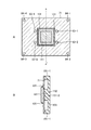
図2は、本技術の回路基板の一実施形態としてのプリント基板71の概略構成を示す図である。図2Aは、プリント基板71の上面図である。図2Bは、図2Aの線a−a’におけるプリント基板71の断面図である。
[Schematic configuration of printed circuit board]
FIG. 2 is a diagram illustrating a schematic configuration of a printed
プリント基板71は、温度調整用開口部81、イメージャマウント用パターン82、イメージャ固定用貫通穴83−1乃至83−4、及びプリント基板固定用貫通穴84−1乃至84−4を備えている。なお、以下、イメージャ固定用貫通穴83−1乃至83−4を個々に区別する必要がない場合、これらをまとめてイメージャ固定用貫通穴83と称する。同様に、プリント基板固定用貫通穴84−1乃至84−4を個々に区別する必要がない場合、これらをまとめてプリント基板固定用貫通穴84と称する。
The printed
温度調整用開口部81は、図3を用いて後述するイメージャ101を実装する位置に設けられ、後述するイメージャ101がプリント基板71に接合可能な範囲内で可能な限り大きな面積となっている。
The
プリント基板71の表面のうち、温度調整用開口部81の外周部には、イメージャマウント用パターン82が形成されている。イメージャマウント用パターン82に対して、後述するイメージャ101に形成されたイメージャマウント用パターン112が、半田により接合されることで、イメージャ101は、プリント基板71の表面に実装される。
An
プリント基板71の表面のうち、イメージャマウント用パターン82の周囲近傍には、イメージャ固定用貫通穴83が設けられている。プリント基板71の表面の四隅には、プリント基板固定用貫通穴84が設けられている。なお、イメージャ固定用貫通穴83及びプリント基板固定用貫通穴84の用途については、後述する。
An imager fixing through hole 83 is provided in the vicinity of the periphery of the
[イメージャの概略構成]
図3は、イメージャ101の概略構成を示す図である。図3Aは、イメージャ101の上面図である。図3Bは、イメージャ101の側面図である。図3Cは、イメージャ101の下面図である。
[Schematic configuration of imager]
FIG. 3 is a diagram showing a schematic configuration of the
図3Aに示されるように、イメージャ101の一面101fの中央部には、受光面111が設けられている。ここで、受光面111が設けられるイメージャ101の一面101fを、イメージャ表面101fと称する。また、イメージャ表面101fと反対側の一面101bを、イメージャ裏面101bと称する。
As shown in FIG. 3A, a
図3Cに示されるように、イメージャ裏面101bの外周部には、イメージャマウント用パターン112が形成されている。イメージャマウント用パターン112が、プリント基板71のイメージャマウント用パターン82(図2)に半田により接合されることで、イメージャ101がプリント基板71の表面に実装される。したがって、プリント基板71のイメージャマウント用パターン82と、イメージャ裏面101bのイメージャマウント用パターン112とは、略同一の寸法を有するように構成される。これにより、イメージャ101は、プリント基板71の表面のうち、温度調整用開口部81を含む領域に接合されることになる。
As shown in FIG. 3C, an
ここで、プリント基板71のイメージャマウント用パターン82と、イメージャ裏面101bのイメージャマウント用パターン112とが半田により接合されることで、プリント基板71とイメージャ101は機械的に接合されると共に、電気的にも接続される。
Here, the
[樹脂による接合]
さらに、プリント基板71とイメージャ101の機械的な接合の強度を増大させるため、両者が樹脂により接合される。
[Joint with resin]
Furthermore, in order to increase the strength of mechanical bonding between the printed
図4は、プリント基板71とイメージャ101の樹脂による接合について説明する図である。図4Aは、イメージャ101が実装されたプリント基板71の上面図である。図4Bは、図4Aの線a−a’におけるプリント基板71の断面図である。
FIG. 4 is a diagram for explaining the bonding of the printed
図4に示されるように、プリント基板71の表面には、半田により接合されたイメージャ101が実装されている。そして、イメージャ101の外周部に示される樹脂131により、プリント基板71とイメージャ101が接合されている。イメージャ101とプリント基板71は、半田による接合に加え、さらに樹脂131によって接合が補強されるので、接合の強度が増大する。
As shown in FIG. 4, the
[ヒートシンクの装着]
次に、イメージャ101の温度を一定に調整するための温度調整部材としてのヒートシンクの装着について説明する。
[Installing heat sink]
Next, mounting of a heat sink as a temperature adjusting member for adjusting the temperature of the
図5は、ヒートシンク151の装着について説明する図である。図5Aは、プリント基板71の上面図である。図5Bは、図5Aの線a−a’におけるプリント基板71の断面図である。
FIG. 5 is a diagram for explaining the mounting of the
図5に示されるように、プリント基板71の裏面にヒートシンク151が装着される。ヒートシンク151は、固定用突起部151−1と接触用突起部151−2を備えている。固定用突起部151−1は、プリント基板71のプリント基板固定用貫通穴84に対応する位置に配置される。また、接触用突起部151−2は、プリント基板71の温度調整用開口部81に対応する位置に配置される。
As shown in FIG. 5, a
固定用突起部151−1の中央部には孔があけられており、図示せぬネジが、プリント基板71のプリント基板固定用貫通穴84及び当該孔に螺挿されることにより、ヒートシンク151がプリント基板71の裏面に装着される。
A hole is formed in the central portion of the fixing protrusion 151-1, and a screw (not shown) is screwed into the printed board fixing through hole 84 of the printed
また、ヒートシンク151の接触用突起部151−2が、温度調整部材としての弾性体の熱伝導シート152を介してイメージャ裏面101bに接着される。すなわち、ヒートシンク151の接触用突起部151−2は、プリント基板71の裏面のうち、温度調整用開口部81を含む領域に、熱伝導シート152を介して装着される。これにより、イメージャ101の熱が、イメージャ裏面101bに接着された熱伝導シート152を介して接触用突起部151−2に伝導され、ヒートシンク151から放熱される。なお、弾性体の熱伝導シート152の換わりに、熱伝導グリスが用いられてもよい。
Further, the contact protrusion 151-2 of the
イメージャ裏面101bからイメージャ101の温度調整を均一に行うために、熱伝導シート152を介して接着されるヒートシンク151の接触用突起部151−2と、イメージャ裏面101bの接触面積は可能な限り大きい方がよい。したがって、プリント基板71とイメージャ101の接合面積は極力小さくして、温度調整用開口部81の面積を大きくする必要がある。しかしながら、プリント基板71とイメージャ101の接合面積が小さくなることで、両者の接合の強度は弱まるため、上述の樹脂131による接合の補強が必要となる。
In order to uniformly adjust the temperature of the
また、イメージャ101からヒートシンク151への熱伝導性を高めるためには、イメージャ裏面101bとヒートシンク151の接触用突起部151−2が、弾性体の熱伝導シート152を介して圧着されていることが望ましい。そのためには、イメージャ101がプリント基板71に強く接合されていることが前提として必要であり、上述の樹脂131による接合の補強が必要となる。
Further, in order to increase the thermal conductivity from the
[イメージャ固定用部材による固定]
このように、イメージャ101とプリント基板71の接合の強度が強いことは、イメージャの効率的な温度調整にとって必要である。したがって、イメージャ101とプリント基板71の接合の強度をより増大させるため、樹脂131による接合の補強に加えて、さらに、イメージャ101は固定用部材によってプリント基板71に固定される。
[Fixing with imager fixing member]
Thus, the strength of the bonding between the
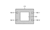
図6は、イメージャ固定用部材171の概略構成を示す図である。
FIG. 6 is a diagram showing a schematic configuration of the
イメージャ固定用部材171は、開口部181、イメージャ固定用部材貫通穴182−1乃至182−4を備えている。なお、イメージャ固定用部材貫通穴182−1乃至182−4を個々に区別する必要がない場合、これらをまとめてイメージャ固定用部材貫通穴182と称する。
The
開口部181は、イメージャ固定用部材171の中央部に形成されており、イメージャ101の受光面111への光を遮らないように、受光面111の面積よりも大きく構成される。
The
イメージャ固定用部材171の開口部181の周囲近傍には、イメージャ固定用部材貫通穴182が設けられている。図示せぬネジが、イメージャ固定用部材貫通穴182及びプリント基板71のイメージャ固定用貫通穴83に螺挿されることにより、イメージャ固定用部材171がプリント基板71に装着される。
An imager fixing member through hole 182 is provided in the vicinity of the periphery of the
図7は、イメージャ固定用部材171の装着について説明する図である。図7Aは、イメージャ固定用部材171が装着されたプリント基板71の上面図である。図7Bは、図7Aの線b−b’におけるプリント基板71の断面図である。
FIG. 7 is a view for explaining the mounting of the
図7に示されるように、イメージャ固定用部材171は、イメージャ101が実装されたプリント基板71の表面に装着される。イメージャ固定用部材171は、イメージャ表面101fに積層され、イメージャ固定用部材171とプリント基板71でイメージャ101を挟み込む状態で、図示せぬネジによりプリント基板71に装着される。これにより、プリント基板71とイメージャ101の半田による接合は、樹脂131及びイメージャ固定用部材171によって補強されるので、接合の強度が増大する。
As shown in FIG. 7, the
図7Bに示されるように、プリント基板71の裏面に装着されたヒートシンク151の接触用突起部151−2には、温度センサ挿入孔191が設けられている。温度センサ挿入孔191には、熱電対やサーミスタ等の図示せぬ温度センサが挿入され、当該温度センサによりイメージャ101の温度が測定される。したがって、温度センサによるイメージャ101の温度の測定がより正確に行われるように、温度センサ挿入孔191は、接触用突起部151−2において、極力イメージャ101に近い位置に設けられる。
As shown in FIG. 7B, a temperature
温度センサによってイメージャ101の温度が測定されることにより、イメージャ101の温度が適正な範囲内にあるか否かの確認が可能となる。
By measuring the temperature of the
なお、上述したように、イメージャ101の熱は、イメージャ裏面101bに接着された熱伝導シート152を介してヒートシンク151の接触用突起部151−2に伝導される。したがって、接触用突起部151−2からヒートシンク151に伝導された熱が、固定用突起部151−1からプリント基板71を介して再びイメージャ101に伝導されないようにする必要がある。このため、ヒートシンク151の固定用突起部151−1は、熱を伝導しない素材により構成されるものとする。
As described above, the heat of the
[プリント基板のその他の概略構成]
次に、イメージャ101を所望の温度に制御するためのプリント基板71の概略構成について説明する。
[Other schematic configuration of printed circuit board]
Next, a schematic configuration of the printed
図8は、イメージャ101を所望の温度に制御するためのプリント基板71の概略構成を示す図である。図8Aは、イメージャ101が実装されたプリント基板71の上面図である。図8Bは、図8Aの線a−a’におけるプリント基板71の断面図である。
FIG. 8 is a diagram showing a schematic configuration of a printed
図8Aに示されるように、プリント基板71の表面には、半田により接合されたイメージャ101が実装されている。そして、イメージャ101の外周部の樹脂131により、プリント基板71とイメージャ101の接合が補強されている。
As shown in FIG. 8A, the
図8Bに示されるように、プリント基板71の裏面には、温度調整プレート201、ペルチェ素子202、板ばね203、及びヒートシンク204が、その順に積層されている。
As shown in FIG. 8B, a
温度調整部材としての温度調整プレート201は、例えば、銅やアルミ等の熱伝導率の高い素材により構成され、温度センサを挿入するための温度センサ挿入孔231が設けられている。温度調整プレート201は、熱伝導シート152を介してイメージャ裏面101bに接着される。
The
温度調整部材としてのペルチェ素子202は、温度調整プレート201と熱伝導性接着剤や銀ペースト等により接着されている。ペルチェ素子202の温度調整プレート201と接着される面を面202Aとし、その反対側の板ばね203が装着される面を面202Bとする。ペルチェ素子202は、電流が通電されると、一方の基板面が吸熱面になり、他方の基板面が発熱面になる。
The
面202Aが吸熱面である場合、反対側の面202Bが発熱面となる。すなわち、所定のプラス電圧値がペルチェ素子202に印加された場合、そのプラス電圧値に応じた温度差△Tが面202Aと面202Bとの間に発生する。これにより、イメージャ101から発せられた熱が面202Aで吸熱され、イメージャ101が冷却される。
When the
また、面202Aが発熱面である場合、反対側の面202Bが吸熱面となる。すなわち、所定のプラス電圧値がペルチェ素子202に印加された場合、そのプラス電圧値に応じた温度差△Tが面202Aと面202Bとの間に発生する。これにより、面202Aの発熱がイメージャ101に伝達され、イメージャ101が加熱される。
When the
このように、ペルチェ素子202によってイメージャ101が冷却又は加熱され、予め設定された温度に調整することが可能となる。
As described above, the
板ばね203は、ペルチェ素子202とヒートシンク204の間に設置され、熱伝導シート152、温度調整プレート201、ペルチェ素子202、及びヒートシンク204を、プリント基板71の裏面に圧着させる。イメージャ101に対して温度調整をするためのユニットであって、熱伝導シート152、温度調整プレート201、ペルチェ素子202、またはヒートシンク204などの1以上の温度調整部材から構成されるユニットを温度調整ユニットと称する。
The
[板ばねの概略構成]
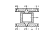
図9は、板ばね203の概略構成を示す図である。
[Schematic configuration of leaf spring]
FIG. 9 is a diagram showing a schematic configuration of the
板ばね203は、開口部211、ヒートシンク取付穴212−1,212−2、及び温度調整ユニット取付穴213−1乃至213−4を備えている。なお、以下、ヒートシンク取付穴212−1,212−2を個々に区別する必要がない場合、これらをまとめてヒートシンク取付穴212と称する。同様に、温度調整ユニット取付穴213−1乃至213−4を個々に区別する必要がない場合、これらをまとめて温度調整ユニット取付穴213と称する。
The
板ばね203は、はじめに、図示せぬネジが、ヒートシンク取付穴212に螺挿されることにより、ヒートシンク204に装着される。その後、図示せぬネジが、板ばね203の温度調整ユニット取付穴213、スペーサ205、プリント基板71のイメージャ固定用貫通穴83に螺挿されることにより、温度調整部材としての温度調整ユニットが、プリント基板71の裏面のうち、温度調整用開口部81を含む領域に圧着される。
The
板ばね203には開口部211が設けられているので、ペルチェ素子202の面202Bとヒートシンク204が接触し、面202Bとヒートシンク204の間での熱伝導が可能となる。
Since the
図8のプリント基板71においても、イメージャ裏面101bからイメージャ101の温度調整を均一に行うために、熱伝導シート152を介して接着される温度調整プレート201と、イメージャ裏面101bの接触面積は可能な限り大きい方がよい。したがって、プリント基板71とイメージャ101の接合面積は極力小さくして、温度調整用開口部81の面積を大きくする必要がある。しかしながら、プリント基板71とイメージャ101の接合面積が小さくなることで、両者の接合の強度は弱まるため、接合の補強が必要となる。
Also in the printed
また、イメージャ101から温度調整ユニットへの熱伝導率を高めるためには、イメージャ裏面101bと温度調整ユニットが、弾性体の熱伝導シート152を介して圧着されていることが望ましい。そのためには、イメージャ101がプリント基板71に強く接合されていることが前提として必要であり、接合の補強が必要となる。
In order to increase the thermal conductivity from the
したがって、プリント基板71とイメージャ101の機械的な接合の強度をより増大させるため、樹脂131による接合の補強に加えて、さらに、図6のイメージャ固定用部材171によって接合を補強し、プリント基板71とイメージャ101の接合の強度をより増大させる。
Therefore, in order to further increase the strength of mechanical bonding between the printed
図8のプリント基板71に、イメージャ固定用部材171が装着された場合の上面図は、図7Aと同様である。しかしながら、イメージャ固定用部材171が装着された図8Aのプリント基板71の、線b−b’における断面図は、図10に示されるようになる。
A top view when the
[イメージャ固定用部材を実装した場合のプリント基板の概略構成]
図10は、図8のプリント基板71にイメージャ固定用部材171が装着された場合の概略構成の断面図である。
[Schematic configuration of the printed circuit board when the imager fixing member is mounted]
FIG. 10 is a cross-sectional view of a schematic configuration when the
図10に示されるように、図示せぬネジが、イメージャ固定用部材171のイメージャ固定用部材貫通穴182、プリント基板71のイメージャ固定用貫通穴83、スペーサ205、及び板ばね203の温度調整ユニット取付穴213に螺挿されることにより、これらが固定される。すなわち、イメージャ101が、イメージャ固定用部材171によってプリント基板71の表面に固定され、温度調整ユニットが、板ばね203によってプリント基板71の裏面に固定される。
As shown in FIG. 10, unillustrated screws are imager fixing member through holes 182 of the
温度調整プレート201に設けられた温度センサ挿入孔231には、熱電対やサーミスタ等の図示せぬ温度センサが挿入され、当該温度センサによりイメージャ101の温度が測定される。温度センサによるイメージャ101の温度の測定がより正確に行われるように、温度センサ挿入孔231は、温度調整プレート201において、極力イメージャ101に近い位置に設けられる。
A temperature sensor (not shown) such as a thermocouple or a thermistor is inserted into the temperature
温度センサによるイメージャ101の測定温度に基づいて、ペルチェ素子202への指令電圧として、所定のプラス電圧値が決定される。そして、その指令電圧がペルチェ素子202に印加されることで、ペルチェ素子202の温度差△Tを可変させ、その結果として、イメージャ101を所望の温度に制御することができる。
Based on the measured temperature of the
このように、プリント基板71に温度調整用開口部81が設けられることにより、ヒートシンク151やペルチェ素子202等の温度調整部材が、プリント基板71を介さずにイメージャ裏面101bに対して直接温度調整をすることができる。すなわち、温度調整部材がプリント基板71を介さずに直接イメージャ101の温度調整を行うことができるため、ファンや恒温槽を設ける必要がなくなり、イメージャ101の受光面111を遮ることなくコンパクトな構造で、効率的な温度調整が可能となる。
Thus, by providing the temperature adjustment opening 81 in the printed
また、本技術においては、イメージャ101とヒートシンク151やペルチェ素子202等の温度調整部材との間に、弾性体の熱伝導シート152が設けられたり、温度調整ユニットが弾性体の板ばね203によって、プリント基板71の裏面に固定される。したがって、機械的な圧着高さの精度を求めなくても、イメージャ101と温度調整部材との間で安定した熱的な結合が可能となる。
Further, in the present technology, an elastic
本技術の実施の形態は、上述した実施の形態に限定されるものではなく、本技術の要旨を逸脱しない範囲において種々の変更が可能である。 Embodiments of the present technology are not limited to the above-described embodiments, and various modifications can be made without departing from the gist of the present technology.
上述の例では、ヒートシンク151やペルチェ素子202等の温度調整部材が、プリント基板71の裏面に配置された。しかしながら、当該温度調整部材は必須の構成要素ではなく、プリント基板71に温度調整用開口部81が設けられることにより、イメージャ101の温度調整の効果を奏することができる。また、プリント基板71の裏面にファン等を配置することで、イメージャ101をイメージャ裏面101bから満遍なく冷却することができるので、イメージャ101の受光面111を遮ることなく温度調整の効果を奏することができる。
In the above-described example, the temperature adjustment members such as the
また、上述の例では、プリント基板71は、顕微鏡システム1の構成要素である撮像装置12のカメラボード31の一部として形成されるかまたは装着されるものとして説明した。しかしながら、これに限定されず、本技術のプリント基板71は、温度調整が必要な部品を実装する回路基板に広く適用することができる。
In the above-described example, the printed
なお、本技術は、以下のような構成もとることができる。
(1)
穴が形成された基板と、
前記基板の表面のうち、前記穴の少なくとも一部を含む第1領域に接合されるイメージャとを備える
回路基板。
(2)
前記基板の裏面のうち、前記穴の少なくとも一部を含む第2領域に、第1の温度調整部材、又は第2の温度調整部材が装着される
前記(1)に記載の回路基板。
(3)
前記イメージャの裏面と前記第1の温度調整部材又は前記第2の温度調整部材との間に、さらに、第3の温度調整部材が挿入される
前記(1)または(2)に記載の回路基板。
(4)
前記第3の温度調整部材は、弾性体の熱伝導体シートを含む
前記(1)、(2)、または(3)に記載の回路基板。
(5)
前記第3の温度調整部材は、熱伝導グリスを含む
前記(1)乃至(4)のいずれかに記載の回路基板。
(6)
前記第1の温度調整部材は、温度センサを挿入する挿入孔を有するヒートシンクである
前記(1)乃至(5)のいずれかに記載の回路基板。
(7)
前記第2領域に装着された前記第2の温度調整部材を、前記第2領域に圧着する弾性体をさらに備える
前記(1)乃至(6)のいずれかに記載の回路基板。
(8)
前記第2の温度調整部材は、温度センサを挿入する挿入孔を有する温度調整プレートを含む
前記(1)乃至(7)のいずれかに記載の回路基板。
(9)
前記基板と前記イメージャは、半田及び樹脂により接合されている
前記(1)乃至(8)のいずれかに記載の回路基板。
(10)
前記第1領域に接合された前記イメージャを、前記第1領域に固定する固定用部材をさらに備える
前記(1)乃至(9)のいずれかに記載の回路基板。
In addition, this technique can also take the following structures.
(1)
A substrate with holes formed therein;
A circuit board comprising: an imager bonded to a first region including at least a part of the hole in the surface of the substrate.
(2)
The circuit board according to (1), wherein the first temperature adjustment member or the second temperature adjustment member is attached to a second region including at least a part of the hole in the back surface of the substrate.
(3)
The circuit board according to (1) or (2), wherein a third temperature adjustment member is further inserted between the back surface of the imager and the first temperature adjustment member or the second temperature adjustment member. .
(4)
The circuit board according to (1), (2), or (3), wherein the third temperature adjustment member includes an elastic heat conductor sheet.
(5)
The circuit board according to any one of (1) to (4), wherein the third temperature adjustment member includes thermal conductive grease.
(6)
The circuit board according to any one of (1) to (5), wherein the first temperature adjustment member is a heat sink having an insertion hole into which a temperature sensor is inserted.
(7)
The circuit board according to any one of (1) to (6), further including an elastic body that press-bonds the second temperature adjustment member attached to the second region to the second region.
(8)
The circuit board according to any one of (1) to (7), wherein the second temperature adjustment member includes a temperature adjustment plate having an insertion hole into which a temperature sensor is inserted.
(9)
The circuit board according to any one of (1) to (8), wherein the substrate and the imager are joined together by solder and resin.
(10)
The circuit board according to any one of (1) to (9), further including a fixing member that fixes the imager joined to the first region to the first region.
本技術は、イメージャを実装する回路基板に適用することができる。 The present technology can be applied to a circuit board on which an imager is mounted.
71 プリント基板, 81 温度調整用開口部, 101 イメージャ, 111 受光面, 131 樹脂, 151 ヒートシンク, 152 熱伝導シート, 171 イメージャ固定用部材, 191 温度センサ挿入孔, 201 温度調整プレート, 202 ペルチェ素子, 203 板ばね, 204 ヒートシンク, 231 温度センサ挿入孔 71 Printed circuit board, 81 Temperature adjustment opening, 101 Imager, 111 Light receiving surface, 131 Resin, 151 Heat sink, 152 Thermal conduction sheet, 171 Imager fixing member, 191 Temperature sensor insertion hole, 201 Temperature adjustment plate, 202 Peltier element, 203 leaf spring, 204 heat sink, 231 temperature sensor insertion hole
Claims (7)
前記基板の表面のうち、前記穴の少なくとも一部を含む第1領域に接合されたイメージャと、
第1の温度調整部材と、
前記基板の裏面のうち、前記穴の少なくとも一部を含む第2領域に装着された第2の温度調整部材と、
前記穴に収容され、前記イメージャと前記第2の温度調整部材に挟持された第3の温度調整部材と、
開口部を有し、前記第1の温度調整部材を前記第2の温度調整部材に押圧させて前記第2の温度調整部材を前記第2領域に圧着させ、前記第2の温度調整部材を前記第3の温度調整部材に押圧する弾性体と
を具備し、
前記第1の温度調整部材は、前記開口部を介して前記第2の温度調整部材と接触する
回路基板。 A substrate with holes formed therein;
An imager joined to a first region of the surface of the substrate that includes at least a portion of the hole;
A first temperature adjustment member;
A second temperature adjustment member attached to a second region including at least a part of the hole in the back surface of the substrate;
A third temperature adjustment member housed in the hole and sandwiched between the imager and the second temperature adjustment member;
Has an opening, the first temperature adjusting member is crimped said second temperature adjusting member is pressed against the second temperature adjusting member to the second region, the said second temperature adjusting member An elastic body that presses against the third temperature adjustment member ,
The first temperature adjustment member is in contact with the second temperature adjustment member through the opening.
請求項1に記載の回路基板。 The circuit board according to claim 1, wherein the third temperature adjustment member includes an elastic heat conductor sheet.
請求項1に記載の回路基板。 The circuit board according to claim 1, wherein the third temperature adjustment member includes thermal conductive grease.
請求項1乃至3のいずれかに記載の回路基板。 The circuit board according to claim 1, wherein the first temperature adjustment member is a heat sink having an insertion hole into which a temperature sensor is inserted.
請求項1乃至4のいずれかに記載の回路基板。 The circuit board according to claim 1, wherein the second temperature adjustment member includes a temperature adjustment plate having an insertion hole into which a temperature sensor is inserted.
請求項1乃至5のいずれかに記載の回路基板。 The circuit board according to claim 1, wherein the substrate and the imager are joined by solder and resin.
請求項1乃至6のいずれかに記載の回路基板。 The circuit board according to claim 1, further comprising a fixing member that fixes the imager joined to the first region to the first region.
Priority Applications (3)
| Application Number | Priority Date | Filing Date | Title |
|---|---|---|---|
| JP2011196819A JP6035015B2 (en) | 2011-09-09 | 2011-09-09 | Circuit board |
| US13/598,269 US9161432B2 (en) | 2011-09-09 | 2012-08-29 | Circuit board |
| CN201210320809.3A CN103002658B (en) | 2011-09-09 | 2012-08-31 | Circuit board |
Applications Claiming Priority (1)
| Application Number | Priority Date | Filing Date | Title |
|---|---|---|---|
| JP2011196819A JP6035015B2 (en) | 2011-09-09 | 2011-09-09 | Circuit board |
Publications (3)
| Publication Number | Publication Date |
|---|---|
| JP2013058663A JP2013058663A (en) | 2013-03-28 |
| JP2013058663A5 JP2013058663A5 (en) | 2014-10-16 |
| JP6035015B2 true JP6035015B2 (en) | 2016-11-30 |
Family
ID=47829088
Family Applications (1)
| Application Number | Title | Priority Date | Filing Date |
|---|---|---|---|
| JP2011196819A Active JP6035015B2 (en) | 2011-09-09 | 2011-09-09 | Circuit board |
Country Status (3)
| Country | Link |
|---|---|
| US (1) | US9161432B2 (en) |
| JP (1) | JP6035015B2 (en) |
| CN (1) | CN103002658B (en) |
Cited By (1)
| Publication number | Priority date | Publication date | Assignee | Title |
|---|---|---|---|---|
| KR101885874B1 (en) * | 2017-05-31 | 2018-08-07 | (주)유진프로텍 | Apparatus for bending metal plate |
Families Citing this family (4)
| Publication number | Priority date | Publication date | Assignee | Title |
|---|---|---|---|---|
| JP6467478B1 (en) * | 2017-09-28 | 2019-02-13 | Kyb株式会社 | Component mounting body and electronic equipment |
| CN107683019B (en) * | 2017-09-30 | 2021-03-30 | 奇酷互联网络科技(深圳)有限公司 | Circuit board, circuit board manufacturing method, temperature detection method and electronic equipment |
| EP3531806B1 (en) * | 2018-02-26 | 2020-03-25 | ZKW Group GmbH | Electronic component board assembly for high performance components |
| CN108490615A (en) * | 2018-03-30 | 2018-09-04 | 京东方科技集团股份有限公司 | VR all-in-one machines |
Family Cites Families (16)
| Publication number | Priority date | Publication date | Assignee | Title |
|---|---|---|---|---|
| JPS62226646A (en) * | 1986-03-27 | 1987-10-05 | Nec Corp | Heat sink |
| JPH0767177B2 (en) | 1993-01-28 | 1995-07-19 | 日本電気株式会社 | Heat dissipation structure of solid-state image sensor |
| JP2002093960A (en) * | 2000-09-12 | 2002-03-29 | Nec Corp | Cooling structure of multichip module and its manufacturing method |
| US6614659B2 (en) * | 2001-12-07 | 2003-09-02 | Delphi Technologies, Inc. | De-mountable, solderless in-line lead module package with interface |
| TW566572U (en) * | 2003-03-07 | 2003-12-11 | Lite On Technology Corp | Flexible assembling device applied in an optical projection apparatus and its mechanism |
| ATE535828T1 (en) * | 2003-06-02 | 2011-12-15 | Seiko Epson Corp | DIGITAL MICRO MIRROR DEVICE ATTACHMENT SYSTEM |
| JP2006054318A (en) * | 2004-08-11 | 2006-02-23 | Seiko Instruments Inc | Electric component module and its manufacturing method |
| JP4722505B2 (en) * | 2005-02-10 | 2011-07-13 | オリンパス株式会社 | Imaging device |
| EP1933609A4 (en) * | 2005-08-30 | 2011-01-05 | Panasonic Corp | SUBSTRATE STRUCTURE |
| JP4715798B2 (en) * | 2007-04-10 | 2011-07-06 | ブラザー工業株式会社 | Electronic equipment |
| TWI345127B (en) * | 2007-11-27 | 2011-07-11 | Coretronic Corp | Dmd module |
| US8148747B2 (en) * | 2008-03-25 | 2012-04-03 | Bridge Semiconductor Corporation | Semiconductor chip assembly with post/base/cap heat spreader |
| JP2010225919A (en) * | 2009-03-24 | 2010-10-07 | Sony Corp | Semiconductor device |
| JP6017107B2 (en) * | 2009-12-28 | 2016-10-26 | ソニー株式会社 | Image sensor, manufacturing method thereof, and sensor device |
| KR101672738B1 (en) * | 2010-08-31 | 2016-11-07 | 삼성전자 주식회사 | electronic device having cooling structure |
| US8737073B2 (en) * | 2011-02-09 | 2014-05-27 | Tsmc Solid State Lighting Ltd. | Systems and methods providing thermal spreading for an LED module |
-
2011
- 2011-09-09 JP JP2011196819A patent/JP6035015B2/en active Active
-
2012
- 2012-08-29 US US13/598,269 patent/US9161432B2/en active Active
- 2012-08-31 CN CN201210320809.3A patent/CN103002658B/en active Active
Cited By (1)
| Publication number | Priority date | Publication date | Assignee | Title |
|---|---|---|---|---|
| KR101885874B1 (en) * | 2017-05-31 | 2018-08-07 | (주)유진프로텍 | Apparatus for bending metal plate |
Also Published As
| Publication number | Publication date |
|---|---|
| CN103002658B (en) | 2017-06-30 |
| US20130062717A1 (en) | 2013-03-14 |
| US9161432B2 (en) | 2015-10-13 |
| JP2013058663A (en) | 2013-03-28 |
| CN103002658A (en) | 2013-03-27 |
Similar Documents
| Publication | Publication Date | Title |
|---|---|---|
| JP6035015B2 (en) | Circuit board | |
| TWI417997B (en) | Heat sink for measuring temperature of electronic component | |
| US7592821B2 (en) | Apparatus and method for managing thermally induced motion of a probe card assembly | |
| US7525816B2 (en) | Wiring board and wiring board connecting apparatus | |
| EP2740260B1 (en) | Device with a housing, at least two printed circuit boards, and at least one heat dissipating element | |
| JP2002261476A (en) | Structure and method for grounding cooling module and electronic apparatus having that structure | |
| JP4438737B2 (en) | Portable electronic devices | |
| WO2003083537A1 (en) | Temperature controller and array waveguide lattice type optical wavelength multiplexer/demultiplexer | |
| JP6607394B2 (en) | Peltier module and peltier module device | |
| JP2011254261A (en) | Camera shake correction unit | |
| US20160165115A1 (en) | Image pickup element unit and image pickup apparatus | |
| JP2016024334A (en) | Display device | |
| KR101702104B1 (en) | Rework station for reworking electronic device including semiconductor device | |
| JP2001308569A (en) | Heat radiating structure of electronic component | |
| JP2002247594A (en) | Image pickup device | |
| JP2015109359A (en) | Thermocompression bonding apparatus | |
| JP2007024702A (en) | Semiconductor inspection socket equipped with heater mechanism | |
| CN209845431U (en) | Drive module and display device | |
| JP2009295626A (en) | Heat radiation structure of electronic device | |
| JP2006086396A (en) | Optical module | |
| JP2003017789A (en) | Optical-module test apparatus and measurement method of optical module characteristics | |
| TWI866444B (en) | Electronic device | |
| JP2006214732A (en) | Reinforcing plate for probe card | |
| JP2012058405A (en) | Camera shake correction unit | |
| CN117835086A (en) | Light small-size integrated area array focal plane system of high thermal stability |
Legal Events
| Date | Code | Title | Description |
|---|---|---|---|
| A521 | Written amendment |
Free format text: JAPANESE INTERMEDIATE CODE: A523 Effective date: 20140902 |
|
| A621 | Written request for application examination |
Free format text: JAPANESE INTERMEDIATE CODE: A621 Effective date: 20140902 |
|
| A131 | Notification of reasons for refusal |
Free format text: JAPANESE INTERMEDIATE CODE: A131 Effective date: 20150428 |
|
| A977 | Report on retrieval |
Free format text: JAPANESE INTERMEDIATE CODE: A971007 Effective date: 20150430 |
|
| A521 | Written amendment |
Free format text: JAPANESE INTERMEDIATE CODE: A523 Effective date: 20150618 |
|
| A131 | Notification of reasons for refusal |
Free format text: JAPANESE INTERMEDIATE CODE: A131 Effective date: 20150707 |
|
| A521 | Written amendment |
Free format text: JAPANESE INTERMEDIATE CODE: A523 Effective date: 20150827 |
|
| A02 | Decision of refusal |
Free format text: JAPANESE INTERMEDIATE CODE: A02 Effective date: 20150929 |
|
| A521 | Written amendment |
Free format text: JAPANESE INTERMEDIATE CODE: A523 Effective date: 20160104 |
|
| A911 | Transfer of reconsideration by examiner before appeal (zenchi) |
Free format text: JAPANESE INTERMEDIATE CODE: A911 Effective date: 20160113 |
|
| A912 | Removal of reconsideration by examiner before appeal (zenchi) |
Free format text: JAPANESE INTERMEDIATE CODE: A912 Effective date: 20160311 |
|
| A521 | Written amendment |
Free format text: JAPANESE INTERMEDIATE CODE: A523 Effective date: 20160729 |
|
| A61 | First payment of annual fees (during grant procedure) |
Free format text: JAPANESE INTERMEDIATE CODE: A61 Effective date: 20161031 |
|
| R150 | Certificate of patent or registration of utility model |
Ref document number: 6035015 Country of ref document: JP Free format text: JAPANESE INTERMEDIATE CODE: R150 |
|
| R250 | Receipt of annual fees |
Free format text: JAPANESE INTERMEDIATE CODE: R250 |
|
| R250 | Receipt of annual fees |
Free format text: JAPANESE INTERMEDIATE CODE: R250 |