JP6024620B2 - Anisotropic conductive film and manufacturing method thereof - Google Patents
Anisotropic conductive film and manufacturing method thereof Download PDFInfo
- Publication number
- JP6024620B2 JP6024620B2 JP2013173195A JP2013173195A JP6024620B2 JP 6024620 B2 JP6024620 B2 JP 6024620B2 JP 2013173195 A JP2013173195 A JP 2013173195A JP 2013173195 A JP2013173195 A JP 2013173195A JP 6024620 B2 JP6024620 B2 JP 6024620B2
- Authority
- JP
- Japan
- Prior art keywords
- connection layer
- layer
- insulating resin
- conductive particles
- connection
- Prior art date
- Legal status (The legal status is an assumption and is not a legal conclusion. Google has not performed a legal analysis and makes no representation as to the accuracy of the status listed.)
- Active
Links
Images


Classifications
-
- H—ELECTRICITY
- H01—ELECTRIC ELEMENTS
- H01L—SEMICONDUCTOR DEVICES NOT COVERED BY CLASS H10
- H01L24/00—Arrangements for connecting or disconnecting semiconductor or solid-state bodies; Methods or apparatus related thereto
- H01L24/01—Means for bonding being attached to, or being formed on, the surface to be connected, e.g. chip-to-package, die-attach, "first-level" interconnects; Manufacturing methods related thereto
- H01L24/26—Layer connectors, e.g. plate connectors, solder or adhesive layers; Manufacturing methods related thereto
- H01L24/28—Structure, shape, material or disposition of the layer connectors prior to the connecting process
- H01L24/29—Structure, shape, material or disposition of the layer connectors prior to the connecting process of an individual layer connector
-
- H—ELECTRICITY
- H01—ELECTRIC ELEMENTS
- H01L—SEMICONDUCTOR DEVICES NOT COVERED BY CLASS H10
- H01L24/00—Arrangements for connecting or disconnecting semiconductor or solid-state bodies; Methods or apparatus related thereto
- H01L24/01—Means for bonding being attached to, or being formed on, the surface to be connected, e.g. chip-to-package, die-attach, "first-level" interconnects; Manufacturing methods related thereto
- H01L24/26—Layer connectors, e.g. plate connectors, solder or adhesive layers; Manufacturing methods related thereto
- H01L24/27—Manufacturing methods
-
- B—PERFORMING OPERATIONS; TRANSPORTING
- B32—LAYERED PRODUCTS
- B32B—LAYERED PRODUCTS, i.e. PRODUCTS BUILT-UP OF STRATA OF FLAT OR NON-FLAT, e.g. CELLULAR OR HONEYCOMB, FORM
- B32B3/00—Layered products comprising a layer with external or internal discontinuities or unevennesses, or a layer of non-planar form; Layered products having particular features of form
- B32B3/26—Layered products comprising a layer with external or internal discontinuities or unevennesses, or a layer of non-planar form; Layered products having particular features of form characterised by a particular shape of the outline of the cross-section of a continuous layer; characterised by a layer with cavities or internal voids ; characterised by an apertured layer
- B32B3/263—Layered products comprising a layer with external or internal discontinuities or unevennesses, or a layer of non-planar form; Layered products having particular features of form characterised by a particular shape of the outline of the cross-section of a continuous layer; characterised by a layer with cavities or internal voids ; characterised by an apertured layer characterised by a layer having non-uniform thickness
-
- B—PERFORMING OPERATIONS; TRANSPORTING
- B32—LAYERED PRODUCTS
- B32B—LAYERED PRODUCTS, i.e. PRODUCTS BUILT-UP OF STRATA OF FLAT OR NON-FLAT, e.g. CELLULAR OR HONEYCOMB, FORM
- B32B37/00—Methods or apparatus for laminating, e.g. by curing or by ultrasonic bonding
- B32B37/02—Methods or apparatus for laminating, e.g. by curing or by ultrasonic bonding characterised by a sequence of laminating steps, e.g. by adding new layers at consecutive laminating stations
- B32B37/025—Transfer laminating
-
- B—PERFORMING OPERATIONS; TRANSPORTING
- B32—LAYERED PRODUCTS
- B32B—LAYERED PRODUCTS, i.e. PRODUCTS BUILT-UP OF STRATA OF FLAT OR NON-FLAT, e.g. CELLULAR OR HONEYCOMB, FORM
- B32B37/00—Methods or apparatus for laminating, e.g. by curing or by ultrasonic bonding
- B32B37/06—Methods or apparatus for laminating, e.g. by curing or by ultrasonic bonding characterised by the heating method
-
- B—PERFORMING OPERATIONS; TRANSPORTING
- B32—LAYERED PRODUCTS
- B32B—LAYERED PRODUCTS, i.e. PRODUCTS BUILT-UP OF STRATA OF FLAT OR NON-FLAT, e.g. CELLULAR OR HONEYCOMB, FORM
- B32B37/00—Methods or apparatus for laminating, e.g. by curing or by ultrasonic bonding
- B32B37/10—Methods or apparatus for laminating, e.g. by curing or by ultrasonic bonding characterised by the pressing technique, e.g. using action of vacuum or fluid pressure
-
- B—PERFORMING OPERATIONS; TRANSPORTING
- B32—LAYERED PRODUCTS
- B32B—LAYERED PRODUCTS, i.e. PRODUCTS BUILT-UP OF STRATA OF FLAT OR NON-FLAT, e.g. CELLULAR OR HONEYCOMB, FORM
- B32B37/00—Methods or apparatus for laminating, e.g. by curing or by ultrasonic bonding
- B32B37/14—Methods or apparatus for laminating, e.g. by curing or by ultrasonic bonding characterised by the properties of the layers
- B32B37/24—Methods or apparatus for laminating, e.g. by curing or by ultrasonic bonding characterised by the properties of the layers with at least one layer not being coherent before laminating, e.g. made up from granular material sprinkled onto a substrate
-
- B—PERFORMING OPERATIONS; TRANSPORTING
- B32—LAYERED PRODUCTS
- B32B—LAYERED PRODUCTS, i.e. PRODUCTS BUILT-UP OF STRATA OF FLAT OR NON-FLAT, e.g. CELLULAR OR HONEYCOMB, FORM
- B32B38/00—Ancillary operations in connection with laminating processes
- B32B38/0008—Electrical discharge treatment, e.g. corona, plasma treatment; wave energy or particle radiation
-
- C—CHEMISTRY; METALLURGY
- C08—ORGANIC MACROMOLECULAR COMPOUNDS; THEIR PREPARATION OR CHEMICAL WORKING-UP; COMPOSITIONS BASED THEREON
- C08G—MACROMOLECULAR COMPOUNDS OBTAINED OTHERWISE THAN BY REACTIONS ONLY INVOLVING UNSATURATED CARBON-TO-CARBON BONDS
- C08G59/00—Polycondensates containing more than one epoxy group per molecule; Macromolecules obtained by polymerising compounds containing more than one epoxy group per molecule using curing agents or catalysts which react with the epoxy groups
- C08G59/18—Macromolecules obtained by polymerising compounds containing more than one epoxy group per molecule using curing agents or catalysts which react with the epoxy groups ; e.g. general methods of curing
- C08G59/68—Macromolecules obtained by polymerising compounds containing more than one epoxy group per molecule using curing agents or catalysts which react with the epoxy groups ; e.g. general methods of curing characterised by the catalysts used
-
- H—ELECTRICITY
- H01—ELECTRIC ELEMENTS
- H01L—SEMICONDUCTOR DEVICES NOT COVERED BY CLASS H10
- H01L24/00—Arrangements for connecting or disconnecting semiconductor or solid-state bodies; Methods or apparatus related thereto
- H01L24/80—Methods for connecting semiconductor or other solid state bodies using means for bonding being attached to, or being formed on, the surface to be connected
- H01L24/83—Methods for connecting semiconductor or other solid state bodies using means for bonding being attached to, or being formed on, the surface to be connected using a layer connector
-
- H—ELECTRICITY
- H05—ELECTRIC TECHNIQUES NOT OTHERWISE PROVIDED FOR
- H05K—PRINTED CIRCUITS; CASINGS OR CONSTRUCTIONAL DETAILS OF ELECTRIC APPARATUS; MANUFACTURE OF ASSEMBLAGES OF ELECTRICAL COMPONENTS
- H05K3/00—Apparatus or processes for manufacturing printed circuits
- H05K3/30—Assembling printed circuits with electric components, e.g. with resistor
- H05K3/32—Assembling printed circuits with electric components, e.g. with resistor electrically connecting electric components or wires to printed circuits
- H05K3/321—Assembling printed circuits with electric components, e.g. with resistor electrically connecting electric components or wires to printed circuits by conductive adhesives
- H05K3/323—Assembling printed circuits with electric components, e.g. with resistor electrically connecting electric components or wires to printed circuits by conductive adhesives by applying an anisotropic conductive adhesive layer over an array of pads
-
- B—PERFORMING OPERATIONS; TRANSPORTING
- B32—LAYERED PRODUCTS
- B32B—LAYERED PRODUCTS, i.e. PRODUCTS BUILT-UP OF STRATA OF FLAT OR NON-FLAT, e.g. CELLULAR OR HONEYCOMB, FORM
- B32B37/00—Methods or apparatus for laminating, e.g. by curing or by ultrasonic bonding
- B32B37/14—Methods or apparatus for laminating, e.g. by curing or by ultrasonic bonding characterised by the properties of the layers
- B32B37/24—Methods or apparatus for laminating, e.g. by curing or by ultrasonic bonding characterised by the properties of the layers with at least one layer not being coherent before laminating, e.g. made up from granular material sprinkled onto a substrate
- B32B2037/243—Coating
-
- B—PERFORMING OPERATIONS; TRANSPORTING
- B32—LAYERED PRODUCTS
- B32B—LAYERED PRODUCTS, i.e. PRODUCTS BUILT-UP OF STRATA OF FLAT OR NON-FLAT, e.g. CELLULAR OR HONEYCOMB, FORM
- B32B2305/00—Condition, form or state of the layers or laminate
- B32B2305/30—Fillers, e.g. particles, powders, beads, flakes, spheres, chips
-
- B—PERFORMING OPERATIONS; TRANSPORTING
- B32—LAYERED PRODUCTS
- B32B—LAYERED PRODUCTS, i.e. PRODUCTS BUILT-UP OF STRATA OF FLAT OR NON-FLAT, e.g. CELLULAR OR HONEYCOMB, FORM
- B32B2307/00—Properties of the layers or laminate
- B32B2307/20—Properties of the layers or laminate having particular electrical or magnetic properties, e.g. piezoelectric
- B32B2307/202—Conductive
-
- B—PERFORMING OPERATIONS; TRANSPORTING
- B32—LAYERED PRODUCTS
- B32B—LAYERED PRODUCTS, i.e. PRODUCTS BUILT-UP OF STRATA OF FLAT OR NON-FLAT, e.g. CELLULAR OR HONEYCOMB, FORM
- B32B2457/00—Electrical equipment
-
- C—CHEMISTRY; METALLURGY
- C09—DYES; PAINTS; POLISHES; NATURAL RESINS; ADHESIVES; COMPOSITIONS NOT OTHERWISE PROVIDED FOR; APPLICATIONS OF MATERIALS NOT OTHERWISE PROVIDED FOR
- C09J—ADHESIVES; NON-MECHANICAL ASPECTS OF ADHESIVE PROCESSES IN GENERAL; ADHESIVE PROCESSES NOT PROVIDED FOR ELSEWHERE; USE OF MATERIALS AS ADHESIVES
- C09J4/00—Adhesives based on organic non-macromolecular compounds having at least one polymerisable carbon-to-carbon unsaturated bond ; adhesives, based on monomers of macromolecular compounds of groups C09J183/00 - C09J183/16
-
- H—ELECTRICITY
- H01—ELECTRIC ELEMENTS
- H01L—SEMICONDUCTOR DEVICES NOT COVERED BY CLASS H10
- H01L2224/00—Indexing scheme for arrangements for connecting or disconnecting semiconductor or solid-state bodies and methods related thereto as covered by H01L24/00
- H01L2224/01—Means for bonding being attached to, or being formed on, the surface to be connected, e.g. chip-to-package, die-attach, "first-level" interconnects; Manufacturing methods related thereto
- H01L2224/26—Layer connectors, e.g. plate connectors, solder or adhesive layers; Manufacturing methods related thereto
- H01L2224/27—Manufacturing methods
- H01L2224/27001—Involving a temporary auxiliary member not forming part of the manufacturing apparatus, e.g. removable or sacrificial coating, film or substrate
- H01L2224/27003—Involving a temporary auxiliary member not forming part of the manufacturing apparatus, e.g. removable or sacrificial coating, film or substrate for holding or transferring the layer preform
-
- H—ELECTRICITY
- H01—ELECTRIC ELEMENTS
- H01L—SEMICONDUCTOR DEVICES NOT COVERED BY CLASS H10
- H01L2224/00—Indexing scheme for arrangements for connecting or disconnecting semiconductor or solid-state bodies and methods related thereto as covered by H01L24/00
- H01L2224/01—Means for bonding being attached to, or being formed on, the surface to be connected, e.g. chip-to-package, die-attach, "first-level" interconnects; Manufacturing methods related thereto
- H01L2224/26—Layer connectors, e.g. plate connectors, solder or adhesive layers; Manufacturing methods related thereto
- H01L2224/27—Manufacturing methods
- H01L2224/27001—Involving a temporary auxiliary member not forming part of the manufacturing apparatus, e.g. removable or sacrificial coating, film or substrate
- H01L2224/27005—Involving a temporary auxiliary member not forming part of the manufacturing apparatus, e.g. removable or sacrificial coating, film or substrate for aligning the layer connector, e.g. marks, spacers
-
- H—ELECTRICITY
- H01—ELECTRIC ELEMENTS
- H01L—SEMICONDUCTOR DEVICES NOT COVERED BY CLASS H10
- H01L2224/00—Indexing scheme for arrangements for connecting or disconnecting semiconductor or solid-state bodies and methods related thereto as covered by H01L24/00
- H01L2224/01—Means for bonding being attached to, or being formed on, the surface to be connected, e.g. chip-to-package, die-attach, "first-level" interconnects; Manufacturing methods related thereto
- H01L2224/26—Layer connectors, e.g. plate connectors, solder or adhesive layers; Manufacturing methods related thereto
- H01L2224/28—Structure, shape, material or disposition of the layer connectors prior to the connecting process
- H01L2224/29—Structure, shape, material or disposition of the layer connectors prior to the connecting process of an individual layer connector
- H01L2224/29001—Core members of the layer connector
- H01L2224/29075—Plural core members
- H01L2224/29076—Plural core members being mutually engaged together, e.g. through inserts
-
- H—ELECTRICITY
- H01—ELECTRIC ELEMENTS
- H01L—SEMICONDUCTOR DEVICES NOT COVERED BY CLASS H10
- H01L2224/00—Indexing scheme for arrangements for connecting or disconnecting semiconductor or solid-state bodies and methods related thereto as covered by H01L24/00
- H01L2224/01—Means for bonding being attached to, or being formed on, the surface to be connected, e.g. chip-to-package, die-attach, "first-level" interconnects; Manufacturing methods related thereto
- H01L2224/26—Layer connectors, e.g. plate connectors, solder or adhesive layers; Manufacturing methods related thereto
- H01L2224/28—Structure, shape, material or disposition of the layer connectors prior to the connecting process
- H01L2224/29—Structure, shape, material or disposition of the layer connectors prior to the connecting process of an individual layer connector
- H01L2224/29001—Core members of the layer connector
- H01L2224/29075—Plural core members
- H01L2224/2908—Plural core members being stacked
- H01L2224/29082—Two-layer arrangements
-
- H—ELECTRICITY
- H01—ELECTRIC ELEMENTS
- H01L—SEMICONDUCTOR DEVICES NOT COVERED BY CLASS H10
- H01L2224/00—Indexing scheme for arrangements for connecting or disconnecting semiconductor or solid-state bodies and methods related thereto as covered by H01L24/00
- H01L2224/01—Means for bonding being attached to, or being formed on, the surface to be connected, e.g. chip-to-package, die-attach, "first-level" interconnects; Manufacturing methods related thereto
- H01L2224/26—Layer connectors, e.g. plate connectors, solder or adhesive layers; Manufacturing methods related thereto
- H01L2224/28—Structure, shape, material or disposition of the layer connectors prior to the connecting process
- H01L2224/29—Structure, shape, material or disposition of the layer connectors prior to the connecting process of an individual layer connector
- H01L2224/29001—Core members of the layer connector
- H01L2224/29075—Plural core members
- H01L2224/2908—Plural core members being stacked
- H01L2224/29083—Three-layer arrangements
-
- H—ELECTRICITY
- H01—ELECTRIC ELEMENTS
- H01L—SEMICONDUCTOR DEVICES NOT COVERED BY CLASS H10
- H01L2224/00—Indexing scheme for arrangements for connecting or disconnecting semiconductor or solid-state bodies and methods related thereto as covered by H01L24/00
- H01L2224/01—Means for bonding being attached to, or being formed on, the surface to be connected, e.g. chip-to-package, die-attach, "first-level" interconnects; Manufacturing methods related thereto
- H01L2224/26—Layer connectors, e.g. plate connectors, solder or adhesive layers; Manufacturing methods related thereto
- H01L2224/28—Structure, shape, material or disposition of the layer connectors prior to the connecting process
- H01L2224/29—Structure, shape, material or disposition of the layer connectors prior to the connecting process of an individual layer connector
- H01L2224/29001—Core members of the layer connector
- H01L2224/29099—Material
- H01L2224/2919—Material with a principal constituent of the material being a polymer, e.g. polyester, phenolic based polymer, epoxy
-
- H—ELECTRICITY
- H01—ELECTRIC ELEMENTS
- H01L—SEMICONDUCTOR DEVICES NOT COVERED BY CLASS H10
- H01L2224/00—Indexing scheme for arrangements for connecting or disconnecting semiconductor or solid-state bodies and methods related thereto as covered by H01L24/00
- H01L2224/01—Means for bonding being attached to, or being formed on, the surface to be connected, e.g. chip-to-package, die-attach, "first-level" interconnects; Manufacturing methods related thereto
- H01L2224/26—Layer connectors, e.g. plate connectors, solder or adhesive layers; Manufacturing methods related thereto
- H01L2224/28—Structure, shape, material or disposition of the layer connectors prior to the connecting process
- H01L2224/29—Structure, shape, material or disposition of the layer connectors prior to the connecting process of an individual layer connector
- H01L2224/29001—Core members of the layer connector
- H01L2224/29099—Material
- H01L2224/29198—Material with a principal constituent of the material being a combination of two or more materials in the form of a matrix with a filler, i.e. being a hybrid material, e.g. segmented structures, foams
- H01L2224/29199—Material of the matrix
- H01L2224/2929—Material of the matrix with a principal constituent of the material being a polymer, e.g. polyester, phenolic based polymer, epoxy
-
- H—ELECTRICITY
- H01—ELECTRIC ELEMENTS
- H01L—SEMICONDUCTOR DEVICES NOT COVERED BY CLASS H10
- H01L2224/00—Indexing scheme for arrangements for connecting or disconnecting semiconductor or solid-state bodies and methods related thereto as covered by H01L24/00
- H01L2224/01—Means for bonding being attached to, or being formed on, the surface to be connected, e.g. chip-to-package, die-attach, "first-level" interconnects; Manufacturing methods related thereto
- H01L2224/26—Layer connectors, e.g. plate connectors, solder or adhesive layers; Manufacturing methods related thereto
- H01L2224/28—Structure, shape, material or disposition of the layer connectors prior to the connecting process
- H01L2224/29—Structure, shape, material or disposition of the layer connectors prior to the connecting process of an individual layer connector
- H01L2224/29001—Core members of the layer connector
- H01L2224/29099—Material
- H01L2224/29198—Material with a principal constituent of the material being a combination of two or more materials in the form of a matrix with a filler, i.e. being a hybrid material, e.g. segmented structures, foams
- H01L2224/29298—Fillers
- H01L2224/29299—Base material
- H01L2224/293—Base material with a principal constituent of the material being a metal or a metalloid, e.g. boron [B], silicon [Si], germanium [Ge], arsenic [As], antimony [Sb], tellurium [Te] and polonium [Po], and alloys thereof
- H01L2224/29338—Base material with a principal constituent of the material being a metal or a metalloid, e.g. boron [B], silicon [Si], germanium [Ge], arsenic [As], antimony [Sb], tellurium [Te] and polonium [Po], and alloys thereof the principal constituent melting at a temperature of greater than or equal to 950°C and less than 1550°C
- H01L2224/29339—Silver [Ag] as principal constituent
-
- H—ELECTRICITY
- H01—ELECTRIC ELEMENTS
- H01L—SEMICONDUCTOR DEVICES NOT COVERED BY CLASS H10
- H01L2224/00—Indexing scheme for arrangements for connecting or disconnecting semiconductor or solid-state bodies and methods related thereto as covered by H01L24/00
- H01L2224/01—Means for bonding being attached to, or being formed on, the surface to be connected, e.g. chip-to-package, die-attach, "first-level" interconnects; Manufacturing methods related thereto
- H01L2224/26—Layer connectors, e.g. plate connectors, solder or adhesive layers; Manufacturing methods related thereto
- H01L2224/28—Structure, shape, material or disposition of the layer connectors prior to the connecting process
- H01L2224/29—Structure, shape, material or disposition of the layer connectors prior to the connecting process of an individual layer connector
- H01L2224/29001—Core members of the layer connector
- H01L2224/29099—Material
- H01L2224/29198—Material with a principal constituent of the material being a combination of two or more materials in the form of a matrix with a filler, i.e. being a hybrid material, e.g. segmented structures, foams
- H01L2224/29298—Fillers
- H01L2224/29299—Base material
- H01L2224/293—Base material with a principal constituent of the material being a metal or a metalloid, e.g. boron [B], silicon [Si], germanium [Ge], arsenic [As], antimony [Sb], tellurium [Te] and polonium [Po], and alloys thereof
- H01L2224/29338—Base material with a principal constituent of the material being a metal or a metalloid, e.g. boron [B], silicon [Si], germanium [Ge], arsenic [As], antimony [Sb], tellurium [Te] and polonium [Po], and alloys thereof the principal constituent melting at a temperature of greater than or equal to 950°C and less than 1550°C
- H01L2224/29344—Gold [Au] as principal constituent
-
- H—ELECTRICITY
- H01—ELECTRIC ELEMENTS
- H01L—SEMICONDUCTOR DEVICES NOT COVERED BY CLASS H10
- H01L2224/00—Indexing scheme for arrangements for connecting or disconnecting semiconductor or solid-state bodies and methods related thereto as covered by H01L24/00
- H01L2224/01—Means for bonding being attached to, or being formed on, the surface to be connected, e.g. chip-to-package, die-attach, "first-level" interconnects; Manufacturing methods related thereto
- H01L2224/26—Layer connectors, e.g. plate connectors, solder or adhesive layers; Manufacturing methods related thereto
- H01L2224/28—Structure, shape, material or disposition of the layer connectors prior to the connecting process
- H01L2224/29—Structure, shape, material or disposition of the layer connectors prior to the connecting process of an individual layer connector
- H01L2224/29001—Core members of the layer connector
- H01L2224/29099—Material
- H01L2224/29198—Material with a principal constituent of the material being a combination of two or more materials in the form of a matrix with a filler, i.e. being a hybrid material, e.g. segmented structures, foams
- H01L2224/29298—Fillers
- H01L2224/29299—Base material
- H01L2224/293—Base material with a principal constituent of the material being a metal or a metalloid, e.g. boron [B], silicon [Si], germanium [Ge], arsenic [As], antimony [Sb], tellurium [Te] and polonium [Po], and alloys thereof
- H01L2224/29338—Base material with a principal constituent of the material being a metal or a metalloid, e.g. boron [B], silicon [Si], germanium [Ge], arsenic [As], antimony [Sb], tellurium [Te] and polonium [Po], and alloys thereof the principal constituent melting at a temperature of greater than or equal to 950°C and less than 1550°C
- H01L2224/29347—Copper [Cu] as principal constituent
-
- H—ELECTRICITY
- H01—ELECTRIC ELEMENTS
- H01L—SEMICONDUCTOR DEVICES NOT COVERED BY CLASS H10
- H01L2224/00—Indexing scheme for arrangements for connecting or disconnecting semiconductor or solid-state bodies and methods related thereto as covered by H01L24/00
- H01L2224/01—Means for bonding being attached to, or being formed on, the surface to be connected, e.g. chip-to-package, die-attach, "first-level" interconnects; Manufacturing methods related thereto
- H01L2224/26—Layer connectors, e.g. plate connectors, solder or adhesive layers; Manufacturing methods related thereto
- H01L2224/28—Structure, shape, material or disposition of the layer connectors prior to the connecting process
- H01L2224/29—Structure, shape, material or disposition of the layer connectors prior to the connecting process of an individual layer connector
- H01L2224/29001—Core members of the layer connector
- H01L2224/29099—Material
- H01L2224/29198—Material with a principal constituent of the material being a combination of two or more materials in the form of a matrix with a filler, i.e. being a hybrid material, e.g. segmented structures, foams
- H01L2224/29298—Fillers
- H01L2224/29299—Base material
- H01L2224/293—Base material with a principal constituent of the material being a metal or a metalloid, e.g. boron [B], silicon [Si], germanium [Ge], arsenic [As], antimony [Sb], tellurium [Te] and polonium [Po], and alloys thereof
- H01L2224/29338—Base material with a principal constituent of the material being a metal or a metalloid, e.g. boron [B], silicon [Si], germanium [Ge], arsenic [As], antimony [Sb], tellurium [Te] and polonium [Po], and alloys thereof the principal constituent melting at a temperature of greater than or equal to 950°C and less than 1550°C
- H01L2224/29355—Nickel [Ni] as principal constituent
-
- H—ELECTRICITY
- H01—ELECTRIC ELEMENTS
- H01L—SEMICONDUCTOR DEVICES NOT COVERED BY CLASS H10
- H01L2224/00—Indexing scheme for arrangements for connecting or disconnecting semiconductor or solid-state bodies and methods related thereto as covered by H01L24/00
- H01L2224/01—Means for bonding being attached to, or being formed on, the surface to be connected, e.g. chip-to-package, die-attach, "first-level" interconnects; Manufacturing methods related thereto
- H01L2224/26—Layer connectors, e.g. plate connectors, solder or adhesive layers; Manufacturing methods related thereto
- H01L2224/28—Structure, shape, material or disposition of the layer connectors prior to the connecting process
- H01L2224/29—Structure, shape, material or disposition of the layer connectors prior to the connecting process of an individual layer connector
- H01L2224/29001—Core members of the layer connector
- H01L2224/29099—Material
- H01L2224/29198—Material with a principal constituent of the material being a combination of two or more materials in the form of a matrix with a filler, i.e. being a hybrid material, e.g. segmented structures, foams
- H01L2224/29298—Fillers
- H01L2224/29299—Base material
- H01L2224/293—Base material with a principal constituent of the material being a metal or a metalloid, e.g. boron [B], silicon [Si], germanium [Ge], arsenic [As], antimony [Sb], tellurium [Te] and polonium [Po], and alloys thereof
- H01L2224/29338—Base material with a principal constituent of the material being a metal or a metalloid, e.g. boron [B], silicon [Si], germanium [Ge], arsenic [As], antimony [Sb], tellurium [Te] and polonium [Po], and alloys thereof the principal constituent melting at a temperature of greater than or equal to 950°C and less than 1550°C
- H01L2224/29357—Cobalt [Co] as principal constituent
-
- H—ELECTRICITY
- H01—ELECTRIC ELEMENTS
- H01L—SEMICONDUCTOR DEVICES NOT COVERED BY CLASS H10
- H01L2224/00—Indexing scheme for arrangements for connecting or disconnecting semiconductor or solid-state bodies and methods related thereto as covered by H01L24/00
- H01L2224/01—Means for bonding being attached to, or being formed on, the surface to be connected, e.g. chip-to-package, die-attach, "first-level" interconnects; Manufacturing methods related thereto
- H01L2224/26—Layer connectors, e.g. plate connectors, solder or adhesive layers; Manufacturing methods related thereto
- H01L2224/28—Structure, shape, material or disposition of the layer connectors prior to the connecting process
- H01L2224/29—Structure, shape, material or disposition of the layer connectors prior to the connecting process of an individual layer connector
- H01L2224/29001—Core members of the layer connector
- H01L2224/29099—Material
- H01L2224/29198—Material with a principal constituent of the material being a combination of two or more materials in the form of a matrix with a filler, i.e. being a hybrid material, e.g. segmented structures, foams
- H01L2224/29298—Fillers
- H01L2224/29299—Base material
- H01L2224/293—Base material with a principal constituent of the material being a metal or a metalloid, e.g. boron [B], silicon [Si], germanium [Ge], arsenic [As], antimony [Sb], tellurium [Te] and polonium [Po], and alloys thereof
- H01L2224/29363—Base material with a principal constituent of the material being a metal or a metalloid, e.g. boron [B], silicon [Si], germanium [Ge], arsenic [As], antimony [Sb], tellurium [Te] and polonium [Po], and alloys thereof the principal constituent melting at a temperature of greater than 1550°C
- H01L2224/29364—Palladium [Pd] as principal constituent
-
- H—ELECTRICITY
- H01—ELECTRIC ELEMENTS
- H01L—SEMICONDUCTOR DEVICES NOT COVERED BY CLASS H10
- H01L2224/00—Indexing scheme for arrangements for connecting or disconnecting semiconductor or solid-state bodies and methods related thereto as covered by H01L24/00
- H01L2224/01—Means for bonding being attached to, or being formed on, the surface to be connected, e.g. chip-to-package, die-attach, "first-level" interconnects; Manufacturing methods related thereto
- H01L2224/26—Layer connectors, e.g. plate connectors, solder or adhesive layers; Manufacturing methods related thereto
- H01L2224/28—Structure, shape, material or disposition of the layer connectors prior to the connecting process
- H01L2224/29—Structure, shape, material or disposition of the layer connectors prior to the connecting process of an individual layer connector
- H01L2224/29001—Core members of the layer connector
- H01L2224/29099—Material
- H01L2224/29198—Material with a principal constituent of the material being a combination of two or more materials in the form of a matrix with a filler, i.e. being a hybrid material, e.g. segmented structures, foams
- H01L2224/29298—Fillers
- H01L2224/29299—Base material
- H01L2224/2939—Base material with a principal constituent of the material being a polymer, e.g. polyester, phenolic based polymer, epoxy
-
- H—ELECTRICITY
- H01—ELECTRIC ELEMENTS
- H01L—SEMICONDUCTOR DEVICES NOT COVERED BY CLASS H10
- H01L2224/00—Indexing scheme for arrangements for connecting or disconnecting semiconductor or solid-state bodies and methods related thereto as covered by H01L24/00
- H01L2224/01—Means for bonding being attached to, or being formed on, the surface to be connected, e.g. chip-to-package, die-attach, "first-level" interconnects; Manufacturing methods related thereto
- H01L2224/26—Layer connectors, e.g. plate connectors, solder or adhesive layers; Manufacturing methods related thereto
- H01L2224/28—Structure, shape, material or disposition of the layer connectors prior to the connecting process
- H01L2224/29—Structure, shape, material or disposition of the layer connectors prior to the connecting process of an individual layer connector
- H01L2224/29001—Core members of the layer connector
- H01L2224/29099—Material
- H01L2224/29198—Material with a principal constituent of the material being a combination of two or more materials in the form of a matrix with a filler, i.e. being a hybrid material, e.g. segmented structures, foams
- H01L2224/29298—Fillers
- H01L2224/29399—Coating material
- H01L2224/294—Coating material with a principal constituent of the material being a metal or a metalloid, e.g. boron [B], silicon [Si], germanium [Ge], arsenic [As], antimony [Sb], tellurium [Te] and polonium [Po], and alloys thereof
-
- H—ELECTRICITY
- H01—ELECTRIC ELEMENTS
- H01L—SEMICONDUCTOR DEVICES NOT COVERED BY CLASS H10
- H01L2224/00—Indexing scheme for arrangements for connecting or disconnecting semiconductor or solid-state bodies and methods related thereto as covered by H01L24/00
- H01L2224/01—Means for bonding being attached to, or being formed on, the surface to be connected, e.g. chip-to-package, die-attach, "first-level" interconnects; Manufacturing methods related thereto
- H01L2224/26—Layer connectors, e.g. plate connectors, solder or adhesive layers; Manufacturing methods related thereto
- H01L2224/28—Structure, shape, material or disposition of the layer connectors prior to the connecting process
- H01L2224/29—Structure, shape, material or disposition of the layer connectors prior to the connecting process of an individual layer connector
- H01L2224/29001—Core members of the layer connector
- H01L2224/29099—Material
- H01L2224/29198—Material with a principal constituent of the material being a combination of two or more materials in the form of a matrix with a filler, i.e. being a hybrid material, e.g. segmented structures, foams
- H01L2224/29298—Fillers
- H01L2224/29499—Shape or distribution of the fillers
-
- H—ELECTRICITY
- H01—ELECTRIC ELEMENTS
- H01L—SEMICONDUCTOR DEVICES NOT COVERED BY CLASS H10
- H01L2224/00—Indexing scheme for arrangements for connecting or disconnecting semiconductor or solid-state bodies and methods related thereto as covered by H01L24/00
- H01L2224/80—Methods for connecting semiconductor or other solid state bodies using means for bonding being attached to, or being formed on, the surface to be connected
- H01L2224/83—Methods for connecting semiconductor or other solid state bodies using means for bonding being attached to, or being formed on, the surface to be connected using a layer connector
- H01L2224/838—Bonding techniques
- H01L2224/8385—Bonding techniques using a polymer adhesive, e.g. an adhesive based on silicone, epoxy, polyimide, polyester
- H01L2224/83851—Bonding techniques using a polymer adhesive, e.g. an adhesive based on silicone, epoxy, polyimide, polyester being an anisotropic conductive adhesive
-
- H—ELECTRICITY
- H01—ELECTRIC ELEMENTS
- H01L—SEMICONDUCTOR DEVICES NOT COVERED BY CLASS H10
- H01L2924/00—Indexing scheme for arrangements or methods for connecting or disconnecting semiconductor or solid-state bodies as covered by H01L24/00
- H01L2924/10—Details of semiconductor or other solid state devices to be connected
- H01L2924/11—Device type
- H01L2924/12—Passive devices, e.g. 2 terminal devices
- H01L2924/1204—Optical Diode
- H01L2924/12042—LASER
-
- H—ELECTRICITY
- H01—ELECTRIC ELEMENTS
- H01L—SEMICONDUCTOR DEVICES NOT COVERED BY CLASS H10
- H01L2924/00—Indexing scheme for arrangements or methods for connecting or disconnecting semiconductor or solid-state bodies as covered by H01L24/00
- H01L2924/15—Details of package parts other than the semiconductor or other solid state devices to be connected
- H01L2924/151—Die mounting substrate
- H01L2924/156—Material
- H01L2924/15786—Material with a principal constituent of the material being a non metallic, non metalloid inorganic material
- H01L2924/15788—Glasses, e.g. amorphous oxides, nitrides or fluorides
-
- H—ELECTRICITY
- H01—ELECTRIC ELEMENTS
- H01L—SEMICONDUCTOR DEVICES NOT COVERED BY CLASS H10
- H01L2924/00—Indexing scheme for arrangements or methods for connecting or disconnecting semiconductor or solid-state bodies as covered by H01L24/00
- H01L2924/15—Details of package parts other than the semiconductor or other solid state devices to be connected
- H01L2924/181—Encapsulation
-
- H—ELECTRICITY
- H05—ELECTRIC TECHNIQUES NOT OTHERWISE PROVIDED FOR
- H05K—PRINTED CIRCUITS; CASINGS OR CONSTRUCTIONAL DETAILS OF ELECTRIC APPARATUS; MANUFACTURE OF ASSEMBLAGES OF ELECTRICAL COMPONENTS
- H05K1/00—Printed circuits
- H05K1/02—Details
- H05K1/03—Use of materials for the substrate
- H05K1/0313—Organic insulating material
- H05K1/0353—Organic insulating material consisting of two or more materials, e.g. two or more polymers, polymer + filler, + reinforcement
- H05K1/0373—Organic insulating material consisting of two or more materials, e.g. two or more polymers, polymer + filler, + reinforcement containing additives, e.g. fillers
-
- H—ELECTRICITY
- H05—ELECTRIC TECHNIQUES NOT OTHERWISE PROVIDED FOR
- H05K—PRINTED CIRCUITS; CASINGS OR CONSTRUCTIONAL DETAILS OF ELECTRIC APPARATUS; MANUFACTURE OF ASSEMBLAGES OF ELECTRICAL COMPONENTS
- H05K2201/00—Indexing scheme relating to printed circuits covered by H05K1/00
- H05K2201/02—Fillers; Particles; Fibers; Reinforcement materials
- H05K2201/0203—Fillers and particles
- H05K2201/0206—Materials
- H05K2201/0215—Metallic fillers
-
- Y—GENERAL TAGGING OF NEW TECHNOLOGICAL DEVELOPMENTS; GENERAL TAGGING OF CROSS-SECTIONAL TECHNOLOGIES SPANNING OVER SEVERAL SECTIONS OF THE IPC; TECHNICAL SUBJECTS COVERED BY FORMER USPC CROSS-REFERENCE ART COLLECTIONS [XRACs] AND DIGESTS
- Y10—TECHNICAL SUBJECTS COVERED BY FORMER USPC
- Y10T—TECHNICAL SUBJECTS COVERED BY FORMER US CLASSIFICATION
- Y10T428/00—Stock material or miscellaneous articles
- Y10T428/24—Structurally defined web or sheet [e.g., overall dimension, etc.]
- Y10T428/24479—Structurally defined web or sheet [e.g., overall dimension, etc.] including variation in thickness
- Y10T428/24521—Structurally defined web or sheet [e.g., overall dimension, etc.] including variation in thickness with component conforming to contour of nonplanar surface
Landscapes
- Engineering & Computer Science (AREA)
- Microelectronics & Electronic Packaging (AREA)
- Computer Hardware Design (AREA)
- Power Engineering (AREA)
- Manufacturing & Machinery (AREA)
- Chemical & Material Sciences (AREA)
- Organic Chemistry (AREA)
- Health & Medical Sciences (AREA)
- Chemical Kinetics & Catalysis (AREA)
- Medicinal Chemistry (AREA)
- Polymers & Plastics (AREA)
- Physics & Mathematics (AREA)
- Fluid Mechanics (AREA)
- Plasma & Fusion (AREA)
- Thermal Sciences (AREA)
- Non-Insulated Conductors (AREA)
- Manufacturing Of Electrical Connectors (AREA)
- Adhesive Tapes (AREA)
- Adhesives Or Adhesive Processes (AREA)
- Electric Connection Of Electric Components To Printed Circuits (AREA)
- Laminated Bodies (AREA)
- Conductive Materials (AREA)
- Combinations Of Printed Boards (AREA)
- Wire Bonding (AREA)
Description
本発明は、異方性導電フィルム及びその製造方法に関する。 The present invention relates to an anisotropic conductive film and a method for producing the same.
ICチップなどの電子部品の実装に異方性導電フィルムは広く使用されており、近年では、高実装密度への適用の観点から、接続信頼性や絶縁性の向上、粒子捕捉効率の向上、製造コストの低減等を目的に、異方性導電接続用の導電粒子を単層で絶縁性接着層に配列させた異方性導電フィルムが提案されている(特許文献1)。 Anisotropic conductive films are widely used for mounting electronic components such as IC chips. In recent years, from the viewpoint of application to high mounting density, improved connection reliability and insulation, improved particle capture efficiency, manufacturing For the purpose of reducing costs and the like, an anisotropic conductive film in which conductive particles for anisotropic conductive connection are arranged in a single layer on an insulating adhesive layer has been proposed (Patent Document 1).
この異方性導電フィルムは、以下のように作成されている。即ち、まず、開口を有する転写型の当該開口に導電粒子を保持させ、その上から転写用の粘着層が形成された粘着フィルムを押し当て、粘着層に導電粒子を一次転写させる。次に、粘着層に付着した導電粒子に対し、異方性導電フィルムの構成要素となる高分子膜を押し当て、加熱加圧することにより導電粒子を高分子膜表面に二次転写させる。次に、導電粒子が二次転写された高分子膜の導電粒子側表面に、導電粒子を覆うように接着層を形成することにより異方性導電フィルムが作成されている。 This anisotropic conductive film is prepared as follows. That is, first, the conductive particles are held in the opening of the transfer mold having the opening, and the adhesive film on which the transfer adhesive layer is formed is pressed from above, and the conductive particles are primarily transferred to the adhesive layer. Next, the polymer particles that constitute the anisotropic conductive film are pressed against the conductive particles attached to the adhesive layer, and the conductive particles are secondarily transferred to the surface of the polymer film by heating and pressing. Next, an anisotropic conductive film is formed by forming an adhesive layer on the conductive particle side surface of the polymer film to which the conductive particles are secondarily transferred so as to cover the conductive particles.
しかしながら、開口を有する転写型を用いて作成した特許文献1の異方性導電フィルムの場合、一次転写並びに二次転写が順調に推移する限り、異方性導電フィルムの接続信頼性、絶縁性、粒子捕捉効率についてはある程度の向上が期待可能かもしれないが、一般的には、二次転写し易くするために、一次転写用の粘着フィルムとして比較的粘着力が低いものを使用し、しかも導電粒子と粘着フィルムとの接触面積を小さくしている。このため、一次転写操作乃至二次転写操作の際に、一次転写しない導電粒子の発生、一次転写した後に粘着フィルムからの導電粒子の剥落や粘着フィルム上での導電粒子の位置ズレ等が生じ、全体の作業効率が低下するということが懸念されている。
However, in the case of the anisotropic conductive film of
他方、一次転写作業を更に高速且つ円滑に進行させるために、粘着フィルムの粘着力をある程度強くして導電粒子を粘着フィルムに安定的に保持しようとすると、高分子膜への二次転写が困難になり、それを避けるために高分子膜の膜性を強くすると、異方性導電フィルムの導通抵抗が増大し、導通信頼性も低下するという問題があった。このように、開口を有する転写型を用いて異方性導電フィルムを作成しようとしても、実際のところ、一次転写並びに二次転写が順調に推移するとは限らず、そのため、異方性導電フィルムに対しては、良好な接続信頼性、良好な絶縁性、及び良好な粒子捕捉効率を同時に実現することが依然として強く求められているのが現状である。 On the other hand, in order to make the primary transfer work faster and smoother, it is difficult to perform secondary transfer to the polymer film if the adhesive force of the adhesive film is increased to some extent and the conductive particles are stably held on the adhesive film. In order to avoid this, if the film property of the polymer film is increased, there is a problem that the conduction resistance of the anisotropic conductive film increases and the conduction reliability also decreases. Thus, even if an anisotropic conductive film is created using a transfer mold having an opening, in practice, primary transfer and secondary transfer are not always smoothly performed. On the other hand, at present, it is still strongly demanded to simultaneously realize good connection reliability, good insulation, and good particle trapping efficiency.
本発明の目的は、以上の従来の技術の問題点を解決することであり、開口を有する転写型を用いて作成したような、導電粒子が単層で配列された異方性導電フィルムにおいて、良好な接続信頼性、良好な絶縁性、及び良好な粒子捕捉効率を実現することである。 An object of the present invention is to solve the above-described problems of the prior art, and in an anisotropic conductive film in which conductive particles are arranged in a single layer, as created using a transfer mold having an opening, To achieve good connection reliability, good insulation, and good particle trapping efficiency.
本発明者は、開口を有する転写型を用いて異方性導電フィルムを作成する際に、導電粒子を一旦粘着フィルムに一次転写させることなく、異方性導電フィルムを構成する絶縁性樹脂層に転写型から直接単層で配列するように転写させ、しかも、隣接する導電粒子間の中央の絶縁性樹脂層厚が、導電粒子近傍の絶縁性樹脂層厚よりも薄くなるように転写させ、更に、導電粒子が単層で配列しているその絶縁性樹脂層の両面を、接着層として機能する絶縁性の樹脂層で挟持することにより、上述の目的が達成されることを見出し、本発明を完成させた。 When the present inventor makes an anisotropic conductive film using a transfer mold having an opening, the conductive resin is temporarily transferred to the adhesive film without temporarily transferring the conductive particles to the adhesive film. Transfer from the transfer mold so as to be arranged in a single layer, and transfer so that the central insulating resin layer thickness between adjacent conductive particles is thinner than the insulating resin layer thickness near the conductive particles, The present invention has found that the above-mentioned object is achieved by sandwiching both surfaces of an insulating resin layer in which conductive particles are arranged in a single layer with an insulating resin layer functioning as an adhesive layer. Completed.
即ち、本発明は、第1接続層が、主として絶縁性樹脂からなる第2接続層と第3接続層とに挟持された3層構造の異方性導電フィルムであって、
第1接続層が、絶縁性樹脂層の第2接続層側の平面方向に導電粒子が単層で配列された構造を有し、隣接する導電粒子間の中央領域の絶縁性樹脂層厚が、導電粒子近傍の絶縁性樹脂層厚よりも薄くなっている異方性導電フィルムを提供する。
That is, the present invention is an anisotropic conductive film having a three-layer structure in which the first connection layer is sandwiched between the second connection layer and the third connection layer mainly made of an insulating resin,
The first connection layer has a structure in which conductive particles are arranged in a single layer in the planar direction on the second connection layer side of the insulating resin layer, and the insulating resin layer thickness in the central region between adjacent conductive particles is Provided is an anisotropic conductive film that is thinner than the thickness of an insulating resin layer in the vicinity of conductive particles.
また、本発明は、上述の異方性導電フィルムの製造方法であって、以下の工程(A)〜(D)を有する製造方法を提供する。 Moreover, this invention is a manufacturing method of the above-mentioned anisotropic conductive film, Comprising: The manufacturing method which has the following process (A)-(D) is provided.
<工程(A)>
開口が形成された転写型の開口内に導電粒子を配置し、開口が形成された転写型の表面に、剥離フィルム上に形成された絶縁性樹脂層を対向させる工程。
<Process (A)>
A step of disposing conductive particles in the opening of the transfer mold in which the opening is formed and causing the insulating resin layer formed on the release film to face the surface of the transfer mold in which the opening is formed.
<工程(B)>
剥離フィルム側から絶縁性樹脂層に対して圧力をかけ、開口内に絶縁性樹脂を押し込んで絶縁性樹脂層の表面に導電粒子を転着させ、それにより、絶縁性樹脂層の平面方向に導電粒子が単層で配列された構造であって、隣接する導電粒子間の中央領域の絶縁性樹脂層厚が、導電粒子近傍の絶縁性樹脂層厚よりも薄くなっている第1接続層を形成する工程。
<Process (B)>
Pressure is applied to the insulating resin layer from the release film side, the insulating resin is pushed into the opening, and the conductive particles are transferred onto the surface of the insulating resin layer, thereby conducting in the plane direction of the insulating resin layer. A structure in which particles are arranged in a single layer, and a first connection layer is formed in which the insulating resin layer thickness in the central region between adjacent conductive particles is thinner than the insulating resin layer thickness in the vicinity of the conductive particles Process.
<工程(C)>
第1接続層の導電粒子側表面に、主として絶縁性樹脂からなる第2接続層を形成する工程。
<Process (C)>
Forming a second connection layer mainly made of an insulating resin on the conductive particle side surface of the first connection layer;
<工程(D)>
第2接続層と反対側の第1接続層の表面に、主として絶縁性樹脂からなる第3接続層を形成する工程。
<Process (D)>
Forming a third connection layer mainly made of an insulating resin on the surface of the first connection layer opposite to the second connection layer;
また、本発明は、上述の異方性導電フィルムの別の製造方法であって、以下の工程(a)〜(c)を有する製造方法を提供する。 Moreover, this invention is another manufacturing method of the above-mentioned anisotropic conductive film, Comprising: The manufacturing method which has the following processes (a)-(c) is provided.
<工程(a)>
開口が形成された転写型の開口内に導電粒子を配置し、開口が形成された転写型の表面に、予め第3接続層が貼り合わされた絶縁性樹脂層を対向させる工程。
<Process (a)>
A step of disposing conductive particles in the opening of the transfer mold in which the opening is formed, and making the insulating resin layer on which the third connection layer is bonded in advance face the surface of the transfer mold in which the opening is formed.
<工程(b)>
剥離フィルム側から絶縁性樹脂層に対して圧力をかけ、開口内に絶縁性樹脂を押し込んで絶縁性樹脂層の表面に導電粒子を転着させ、それにより、絶縁性樹脂層の平面方向に導電粒子が単層で配列された構造であって、隣接する導電粒子間の中央領域の絶縁性樹脂層厚が、導電粒子近傍の絶縁性樹脂層厚よりも薄くなっている第1接続層を形成する工程。
<Step (b)>
Pressure is applied to the insulating resin layer from the release film side, the insulating resin is pushed into the opening, and the conductive particles are transferred onto the surface of the insulating resin layer, thereby conducting in the plane direction of the insulating resin layer. A structure in which particles are arranged in a single layer, and a first connection layer is formed in which the insulating resin layer thickness in the central region between adjacent conductive particles is thinner than the insulating resin layer thickness in the vicinity of the conductive particles Process.
<工程(c)>
第1接続層の導電粒子側表面に、主として絶縁性樹脂からなる第2接続層を形成する工程。
<Step (c)>
Forming a second connection layer mainly made of an insulating resin on the conductive particle side surface of the first connection layer;
また、本発明は、上述の異方性導電フィルムで第1電子部品を第2電子部品に異方性導電接続してなる接続構造体を提供する。 Moreover, this invention provides the connection structure formed by anisotropically conducting the 1st electronic component to the 2nd electronic component with the above-mentioned anisotropic conductive film.
また、本発明は、上述の異方性導電フィルムで第1電子部品を第2電子部品に異方性導電接続する接続方法であって、
第2電子部品に対し、異方性導電フィルムをその第3接続層側から仮貼りし、仮貼りされた異方性導電フィルムに対し、第1電子部品を搭載し、第1電子部品側から熱圧着する接続方法を提供する。
The present invention also provides a connection method for anisotropically conductively connecting a first electronic component to a second electronic component using the above-described anisotropic conductive film,
An anisotropic conductive film is temporarily attached to the second electronic component from the third connection layer side, and the first electronic component is mounted on the temporarily attached anisotropic conductive film from the first electronic component side. A connection method for thermocompression bonding is provided.
第1接続層が絶縁性の第2接続層と第3接続層とに挟持された3層構造の本発明の異方性導電フィルムは、第1接続層が、絶縁性樹脂層の第2接続層側の平面方向に導電粒子が単層で配列された構造を有し、隣接する導電粒子間の中央の絶縁性樹脂層厚が、導電粒子近傍の絶縁性樹脂層厚よりも薄くなっている構造を有する。このため、導電粒子が単層で配列された異方性導電フィルムにおいて、良好な接続信頼性、良好な絶縁性、及び良好な粒子捕捉効率を実現できる。 In the anisotropic conductive film of the present invention having a three-layer structure in which the first connection layer is sandwiched between the insulating second connection layer and the third connection layer, the first connection layer is the second connection of the insulating resin layer. It has a structure in which conductive particles are arranged in a single layer in the plane direction on the layer side, and the insulating resin layer thickness at the center between adjacent conductive particles is thinner than the insulating resin layer thickness near the conductive particles It has a structure. For this reason, in the anisotropic conductive film in which the conductive particles are arranged in a single layer, it is possible to realize good connection reliability, good insulation, and good particle capturing efficiency.
以下、本発明の異方性導電フィルムを詳細に説明する。 Hereinafter, the anisotropic conductive film of the present invention will be described in detail.
<<異方性導電フィルム>>
図1Aに示すように、本発明の異方性導電フィルム100は、第1接続層1が、主として絶縁性樹脂からなる第2接続層2と第3接続層3とに挟持された3層構造を有する。この第1接続層1は、絶縁性樹脂層10の第2接続層2側の平面方向に導電粒子4が単層で配列されている構造を有する。この場合、導電粒子4は、平面方向に最密充填されていてもよいが、導電粒子4が平面方向に一定の間隔をあけて規則的に(例えば、正方格子状に)配列されていることが好ましい。また、隣接する導電粒子4間の中央領域の絶縁性樹脂層厚t1が、導電粒子4の近傍の絶縁性樹脂層厚t2よりも薄くなっている構造を有する。絶縁性樹脂層厚t1が絶縁性樹脂層厚t2よりも薄くなっていると、異方性導電接続の際、接続すべき端子間に存在せずに利用されなかった導電粒子4は、図1Bに示すように、異方性導電接続の際の加熱加圧により導電粒子4間の絶縁性樹脂層が溶断して導電粒子4を被覆して被覆層1dを形成することができるため、ショートの発生を抑制することができる。
<< anisotropic conductive film >>
As shown in FIG. 1A, the anisotropic
ここで、隣接する導電粒子4間の中央領域とは、図1Aに示すように、隣接する導電粒子間距離Lの中間点Pを中心として±L/4以内の領域である。また、導電粒子近傍とは、第1接続層1の層厚方向で導電粒子4に接する線分付近の位置を意味する。
Here, the central region between the adjacent
なお、絶縁性樹脂層厚t1と絶縁性樹脂層厚t2とは、更に、以下の関係を有することが好ましい。これは、t1がt2に対し薄すぎると導電粒子4が流動し易くなって粒子捕捉効率が低下する傾向があり、また、t2の厚さに近づきすぎると、本発明の効果が得られに難くなる傾向があるからである。
Insulating resin layer thickness t1 and insulating resin layer thickness t2 preferably further have the following relationship. This is because when t1 is too thin with respect to t2, the
![]()
![]()
また、絶縁性樹脂層厚t1の絶対厚としては、薄すぎると第1接続層1を形成し難くなることが懸念されるので、好ましくは0.5μm以上である。他方、絶縁性樹脂層厚t2の絶対厚としては、厚すぎると絶縁性樹脂層10が異方性導電接続の際に接続領域から排除され難くなって導通不良が生ずることが懸念されるので、好ましくは6μm以下である。
Further, the absolute thickness of the insulating resin layer thickness t1 is preferably 0.5 μm or more because there is a concern that it is difficult to form the
なお、図1Cに示すように、導電粒子を含む樹脂層の厚みが平面方向で大きく変動し、その結果、当該樹脂層が分断されるように存在している場合には、導電粒子4間の絶縁性樹脂層厚が実質的に0となってもよい。実質的に0とは導電粒子を含む絶縁性樹脂層が個々に独立して存在している状態を意味する。このような場合には、上述の式の適用はできないので、良好な接続信頼性、良好な絶縁性、及び良好な粒子捕捉効率を実現するためには、導電粒子4の中心を通る垂線と絶縁性樹脂層厚が最も薄い位置との最短距離L1、L2、L3、L4・・を制御することで好ましく行うことができる。即ち、この最短距離L1、L2、L3・・・が長くなると、第1接続層1の樹脂量が相対的に増大し、生産性が向上し、導電粒子4の流動を抑制できる。他方、この最短距離L1、L2、L3、L4・・・が短くなると、第1接続層1の樹脂量が相対的に減少し、粒子間距離を容易に制御することができる。換言すれば、導電粒子の位置合わせの精度を向上させることができる。好ましい距離L1、L2、L3、L4・・・は、導電粒子4の粒子径の好ましくは0.5倍より大きく1.5倍未満、より好ましくは0.6〜1.2倍の範囲である。
In addition, as shown in FIG. 1C, when the thickness of the resin layer containing the conductive particles varies greatly in the plane direction, and as a result, the resin layer is present so as to be divided, the space between the
また、図1Cに示すように、導電粒子4が第1接続層1に埋没していてもよい。浅く埋没するか深く埋没するかという埋没の程度は、第1接続層1の形成時の材料の粘度や、導電粒子を配列した転写型の開口の形状、大きさ等によって変化するが、特に、開口の基底径と開口径との関係で制御することができる。例えば、基底径は導電粒子径の1.1倍以上2倍未満とし、開口径を導電粒子径の1.3倍以上3倍未満とすることが好ましい。
Moreover, as shown in FIG. 1C, the
なお、本発明の効果を損なわない範囲で、図1Cにおいて点線で示すように、導電粒子4′が第2接続層2に存在していてもよい。
In addition, as long as the effect of this invention is not impaired, as shown with a dotted line in FIG. 1C, the electroconductive particle 4 'may exist in the
<第1接続層>
このような第1接続層1を構成する絶縁性樹脂層10としては、公知の絶縁性樹脂層を適宜採用することができる。例えば、アクリレート化合物と熱又は光ラジカル重合開始剤とを含む熱又は光ラジカル重合型樹脂層又はそれを熱又は光ラジカル重合させたもの、またはエポキシ化合物と熱又は光カチオン若しくはアニオン重合開始剤とを含む熱又は光カチオン若しくはアニオン重合型樹脂層又はそれを熱又は光カチオン重合若しくはアニオン重合させたものを採用することができる。
<First connection layer>
As the insulating
中でも、第1接続層1を構成する絶縁性樹脂層10として、アクリレート化合物と熱ラジカル重合開始剤とを含む熱ラジカル重合型樹脂層を採用してもよいが、アクリレート化合物と光ラジカル重合開始剤とを含む光ラジカル重合型樹脂層を採用することが好ましい。これにより、光ラジカル重合型樹脂層に紫外線を照射して光ラジカル重合させて第1接続層1を形成することができる。この場合、第2接続層2の形成前に、導電粒子側から光ラジカル重合型樹脂層に紫外線を照射して光ラジカル重合させると、図1Aに示すように、第1接続層1において、導電粒子4と第3接続層3の表面3aとの間に位置する領域1Xの硬化率を、互いに隣接する導電粒子間に位置する領域1Yの硬化率よりも低くすることができる。従って、第1接続層における硬化率の低い領域1Xの最低溶融粘度を第1接続層における硬化率の高い領域1Yの最低溶融粘度よりも小さくすることができ、異方性導電接続の際に、導電粒子4の位置ズレを防止し、粒子捕捉効率を向上させ、導電粒子4の押し込み性を向上させ、導通抵抗値を低下させ、良好な導通信頼性を実現することができる。
Among them, as the insulating
ここで、硬化率は重合に寄与する官能基(例えばビニル基)の減少比率として定義される数値である。具体的には、硬化後のビニル基の存在量が硬化前の20%であれば、硬化率は80%となる。ビニル基の存在量の測定は、赤外吸収スペクトルのビニル基の特性吸収分析により行うことができる。 Here, the curing rate is a numerical value defined as a reduction ratio of functional groups (for example, vinyl groups) that contribute to polymerization. Specifically, if the vinyl group content after curing is 20% before curing, the curing rate is 80%. The abundance of vinyl groups can be measured by characteristic absorption analysis of vinyl groups in the infrared absorption spectrum.
このように定義される、領域1Xの硬化率は好ましくは40〜80%であり、他方、領域1Yの硬化率は好ましくは70〜100%である。 The curing rate of the region 1X defined as described above is preferably 40 to 80%, while the curing rate of the region 1Y is preferably 70 to 100%.
また、レオメーターで測定した、第1接続層1の最低溶融粘度は、第2接続層2及び第3接続層3のそれぞれの最低溶融粘度よりも高いことが好ましい。具体的には[第1接続層1の最低溶融粘度(mPa・s)]/[第2接続層2又は第3接続層3の最低溶融粘度(mPa・s)]の数値が、低すぎると粒子捕捉効率が低下し、ショート発生の確率が上昇する傾向があり、高すぎると導通信頼性が低下する傾向があるので、好ましくは1〜1000、より好ましくは4〜400である。なお、それぞれの好ましい最低溶融粘度は、前者については、低すぎると粒子捕捉効率が低下する傾向があり、高すぎると導通抵抗値が大きくなる傾向があるので、好ましくは100〜100000mPa・s、より好ましくは500〜50000mPa・sである。後者については、低すぎるとリールにした際に樹脂のはみ出しが生ずる傾向があり、高すぎると導通抵抗値が高くなる傾向があるので、好ましくは0.1〜10000mPa・s、より好ましくは1〜1000mPa・sである。
Moreover, it is preferable that the minimum melt viscosity of the
<アクリレート化合物>
第1接続層1を構成する絶縁性樹脂層10に使用するアクリレート化合物としては、従来公知のラジカル重合性アクリレートを使用することができる。例えば、単官能(メタ)アクリレート(ここで、(メタ)アクリレートにはアクリレートとメタクリレートとが包含される)、二官能以上の多官能(メタ)アクリレートを使用することができる。本発明においては、接着剤を熱硬化性とするために、アクリル系モノマーの少なくとも一部に多官能(メタ)アクリレートを使用することが好ましい。
<Acrylate compound>
As the acrylate compound used for the insulating
単官能(メタ)アクリレートとしては、メチル(メタ)アクリレート、エチル(メタ)アクリレート、n−プロピル(メタ)アクリレート、i−プロピル(メタ)アクリレート、n−ブチル(メタ)アクリレート、i−ブチル(メタ)アクリレート、t−ブチル(メタ)アクリレート、2−メチルブチル(メタ)アクリレート、n−ペンチル(メタ)アクリレート、n−ヘキシル(メタ)アクリレート、n−ヘプチル(メタ)アクリレート、2−メチルヘキシル(メタ)アクリレート、2−エチルヘキシル(メタ)アクリレート、2−ブチルヘキシル(メタ)アクリレート、イソオクチル(メタ)アクリレート、イソペンチル(メタ)アクリレート、イソノニル(メタ)アクリレート、イソデシル(メタ)アクリレート、イソボルニル(メタ)アクリレート、シクロヘキシル(メタ)アクリレート、ベンジル(メタ)アクリレート、フェノキシ(メタ)アクリレート、n−ノニル(メタ)アクリレート、n−デシル(メタ)アクリレート、ラウリル(メタ)アクリレート、ヘキサデシル(メタ)アクリレート、ステアリル(メタ)アクリレート、モルホリン−4−イル(メタ)アクリレート等が挙げられる。二官能(メタ)アクリレートとしては、ビスフェノールF―EO変性ジ(メタ)アクリレート、ビスフェノールA−EO変性ジ(メタ)アクリレート、ポリプロピレングリコールジ(メタ)アクリレート、ポリエチレングリコール(メタ)アクリレート、トリシクロデカンジメチロールジ(メタ)アクリレート、ジシクロペンタジエン(メタ)アクリレート等が挙げられる。三官能(メタ)アクリレートとしては、トリメチロールプロパントリ(メタ)アクリレート、トリメチロールプロパンPO変性(メタ)アクリレート、イソシアヌル酸EO変性トリ(メタ)アクリレート等が挙げられる。四官能以上の(メタ)アクリレートとしては、ジペンタエリスリトールペンタ(メタ)アクリレート、ペンタエリスリトールヘキサ(メタ)アクリレート、ペンタエリスリトールテトラ(メタ)アクリレート、ジトリメチロールプロパンテトラアクリレート等が挙げられる。その他に、多官能ウレタン(メタ)アクリレートも使用することができる。具体的には、M1100、M1200、M1210、M1600(以上、東亞合成(株))、AH−600、AT−600(以上、共栄社化学(株))等が挙げられる。 Monofunctional (meth) acrylates include methyl (meth) acrylate, ethyl (meth) acrylate, n-propyl (meth) acrylate, i-propyl (meth) acrylate, n-butyl (meth) acrylate, i-butyl (meth) ) Acrylate, t-butyl (meth) acrylate, 2-methylbutyl (meth) acrylate, n-pentyl (meth) acrylate, n-hexyl (meth) acrylate, n-heptyl (meth) acrylate, 2-methylhexyl (meth) Acrylate, 2-ethylhexyl (meth) acrylate, 2-butylhexyl (meth) acrylate, isooctyl (meth) acrylate, isopentyl (meth) acrylate, isononyl (meth) acrylate, isodecyl (meth) acrylate, isobornyl (meth) Acrylate, cyclohexyl (meth) acrylate, benzyl (meth) acrylate, phenoxy (meth) acrylate, n-nonyl (meth) acrylate, n-decyl (meth) acrylate, lauryl (meth) acrylate, hexadecyl (meth) acrylate, stearyl ( And (meth) acrylate, morpholin-4-yl (meth) acrylate, and the like. Bifunctional (meth) acrylates include bisphenol F-EO modified di (meth) acrylate, bisphenol A-EO modified di (meth) acrylate, polypropylene glycol di (meth) acrylate, polyethylene glycol (meth) acrylate, and tricyclodecanedi. Examples include methylol di (meth) acrylate and dicyclopentadiene (meth) acrylate. Examples of the trifunctional (meth) acrylate include trimethylolpropane tri (meth) acrylate, trimethylolpropane PO-modified (meth) acrylate, and isocyanuric acid EO-modified tri (meth) acrylate. Examples of tetrafunctional or higher functional (meth) acrylates include dipentaerythritol penta (meth) acrylate, pentaerythritol hexa (meth) acrylate, pentaerythritol tetra (meth) acrylate, and ditrimethylolpropane tetraacrylate. In addition, polyfunctional urethane (meth) acrylates can also be used. Specific examples include M1100, M1200, M1210, M1600 (above, Toagosei Co., Ltd.), AH-600, AT-600 (above, Kyoeisha Chemical Co., Ltd.), and the like.
第1接続層1を構成する絶縁性樹脂層10におけるアクリレート化合物の含有量は、少なすぎると第2接続層2との最低溶融粘度差をつけにくくなる傾向があり、多すぎると硬化収縮が大きくなって作業性が低下する傾向があるので、好ましくは2〜70質量%、より好ましくは10〜50質量%である。
If the content of the acrylate compound in the insulating
<光ラジカル重合開始剤>
光ラジカル重合開始剤としては、公知の光ラジカル重合開始剤の中から適宜選択して使用することができる。たとえは、アセトフェノン系光重合開始剤、ベンジルケタール系光重合開始剤、リン系光重合開始剤等が挙げられる。具体的には、アセトフェノン系光重合開始剤として、2−ヒドロキシ−2−シクロへキシルアセトフェノン(イルガキュア(IRGACURE)184、BASFジャパン(株))、α−ヒドロキシ−α,α′−ジメチルアセトフェノン(ダロキュア(DAROCUR)1173、BASFジャパン(株))、2,2−ジメトキシ−2−フェニルアセトフェノン(イルガキュア(IRGACURE)651、BASFジャパン(株))、4−(2−ヒドロキシエトキシ)フェニル(2−ヒドロキシ−2−プロピル)ケトン(ダロキュア(DAROCUR)2959、BASFジャパン(株))、2−ヒドロキシ−1−{4−[2−ヒドロキシ−2−メチル−プロピオニル]−ベンジル}フェニル}−2−メチル−プロパン−1−オン(イルガキュア(IRGACURE)127、BASFジャパン(株))等が挙げられる。ベンジルケタール系光重合開始剤として、ベンゾフェノン、フルオレノン、ジベンゾスベロン、4−アミノベンゾフェノン、4,4′−ジアミノベンゾフェノン、4−ヒドロキシベンゾフェノン、4−クロロベンゾフェノン、4,4′−ジクロロベンゾフェノン等が挙げられる。また、2−ベンジル−2−ジメチルアミノ−1−(4−モルフォリノフェニル)−ブタノン−1(イルガキュア(IRGACURE)369、BASFジャパン(株))も使用することができる。リン系光重合開始剤として、ビス(2,4,6−トリメチルベンゾイル)−フェニルフォスフィンオキサイド(イルガキュア(IRGACURE)819、BASFジャパン(株))、(2,4,6−トリメチルベンゾイル−ジフェニルフォスフィンオキサイド(ダロキュア(DAROCURE)TPO、BASFジャパン(株))等が挙げられる。
<Radical radical polymerization initiator>
As a radical photopolymerization initiator, it can be used by appropriately selecting from known radical photopolymerization initiators. For example, an acetophenone photopolymerization initiator, a benzyl ketal photopolymerization initiator, a phosphorus photopolymerization initiator, and the like can be given. Specifically, as the acetophenone photopolymerization initiator, 2-hydroxy-2-cyclohexylacetophenone (IRGACURE 184, BASF Japan Ltd.), α-hydroxy-α, α′-dimethylacetophenone (Darocur) (DAROCUR) 1173, BASF Japan Ltd., 2,2-dimethoxy-2-phenylacetophenone (IRGACURE 651, BASF Japan Ltd.), 4- (2-hydroxyethoxy) phenyl (2-hydroxy-) 2-propyl) ketone (DAROCUR 2959, BASF Japan Ltd.), 2-hydroxy-1- {4- [2-hydroxy-2-methyl-propionyl] -benzyl} phenyl} -2-methyl-propane -1-On (Iraki A (IRGACURE) 127, BASF Japan Ltd.) and the like. Examples of the benzyl ketal photopolymerization initiator include benzophenone, fluorenone, dibenzosuberone, 4-aminobenzophenone, 4,4'-diaminobenzophenone, 4-hydroxybenzophenone, 4-chlorobenzophenone, 4,4'-dichlorobenzophenone, and the like. It is done. Further, 2-benzyl-2-dimethylamino-1- (4-morpholinophenyl) -butanone-1 (IRGACURE 369, BASF Japan Ltd.) can also be used. As phosphorous photopolymerization initiators, bis (2,4,6-trimethylbenzoyl) -phenylphosphine oxide (IRGACURE 819, BASF Japan Ltd.), (2,4,6-trimethylbenzoyl-diphenylphossine) Examples include fin oxide (DAROCURE TPO, BASF Japan Ltd.).
光ラジカル重合開始剤の使用量は、アクリレート化合物100質量部に対し、少なすぎると、光ラジカル重合が十分に進行しない傾向があり、多すぎると剛性低下の原因となることが懸念されるので、好ましくは0.1〜25質量部、より好ましくは0.5〜15質量部である。 If the amount of the radical photopolymerization initiator used is too small relative to 100 parts by mass of the acrylate compound, the photoradical polymerization tends not to proceed sufficiently. Preferably it is 0.1-25 mass parts, More preferably, it is 0.5-15 mass parts.
<熱ラジカル重合開始剤>
また、熱ラジカル重合開始剤としては、例えば、有機過酸化物やアゾ系化合物等が挙げられるが、気泡の原因となる窒素を発生しない有機過酸化物を好ましく使用することができる。
<Thermal radical polymerization initiator>
Further, examples of the thermal radical polymerization initiator include organic peroxides and azo compounds, but organic peroxides that do not generate nitrogen that causes bubbles can be preferably used.
有機過酸化物としては、メチルエチルケトンパーオキサイド、シクロヘキサノンパーオキサイド、メチルシクロヘキサノンパーオキサイド、アセチルアセトンパーオキサイド、1,1−ビス(tert−ブチルパーオキシ)3,3,5−トリメチルシクロヘキサン、1,1−ビス(tert−ブチルパーオキシ)シクロヘキサン、1,1−ビス(tert−ヘキシルパーオキシ)3,3,5−トリメチルシクロヘキサン、1,1−ビス(tert−ヘキシルパーオキシ)シクロヘキサン、1,1−ビス(tert−ブチルパーオキシ)シクロドデカン、イソブチルパーオキサイド、過酸化ラウロイル、琥珀酸パーオキサイド、3,5,5−トリメチルヘキサノイルパーオキサイド、過酸化ベンゾイル、オクタノイルパーオキサイド、ステアロイルパーオキサイド、ジイソプロピルパーオキシジカルボネート、ジノルマルプロピルパーオキシジカルボネート、ジ−2−エチルヘキシルパーオキシジカルボネート、ジ−2−エトキシエチルパーオキシジカルボネート、ジ−2−メトキシブチルパーオキシジカルボネート、ビス−(4−tert−ブチルシクロヘキシル)パーオキシジカルボネート、(α,α−ビス−ネオデカノイルパーオキシ)ジイソプロピルベンゼン、パーオキシネオデカン酸クミルエステル、パーオキシネオデカン酸オクチルエステル、パーオキシネオデカン酸ヘキシルエステル、パーオキシネオデカン酸−tert−ブチルエステル、パーオキシピバリン酸−tert−ヘキシルエステル、パーオキシピバリン酸−tert−ブチルエステル、2,5−ジメチル−2,5−ビス(2−エチルヘキサノイルパーオキシ)ヘキサン、1,1,3,3−テトラメチルブチルパーオキシ−2−エチルヘキサノエート、パーオキシ−2−エチルヘキサン酸−tert−ヘキシルエステル、パーオキシ−2−エチルヘキサン酸−tert−ブチルエステル、パーオキシ−2−エチルヘキサン酸−tert−ブチルエステル、パーオキシ−3−メチルプロピオン酸−tert−ブチルエステル、パーオキシラウリン酸−tert−ブチルエステル、tert−ブチルパーオキシ−3,5,5−トリメチルヘキサノエート、tert−ヘキシルパーオキシイソプロピルモノカルボネート、tert−ブチルパーオキシイソプロピルカルボネート、2,5−ジメチル−2,5−ビス(ベンゾイルパーオキシ)ヘキサン、過酢酸−tert−ブチルエステル、過安息香酸−tert−ヘキシルエステル、過安息香酸−tert−ブチルエステルなどが挙げられる。有機過酸物に還元剤を添加し、レドックス系重合開始剤として使用してもよい。 Examples of organic peroxides include methyl ethyl ketone peroxide, cyclohexanone peroxide, methylcyclohexanone peroxide, acetylacetone peroxide, 1,1-bis (tert-butylperoxy) 3,3,5-trimethylcyclohexane, 1,1-bis. (Tert-butylperoxy) cyclohexane, 1,1-bis (tert-hexylperoxy) 3,3,5-trimethylcyclohexane, 1,1-bis (tert-hexylperoxy) cyclohexane, 1,1-bis ( tert-butylperoxy) cyclododecane, isobutyl peroxide, lauroyl peroxide, oxalic acid peroxide, 3,5,5-trimethylhexanoyl peroxide, benzoyl peroxide, octanoyl peroxide, stearoyl peroxide Diisopropyl peroxydicarbonate, dinormalpropyl peroxydicarbonate, di-2-ethylhexyl peroxydicarbonate, di-2-ethoxyethyl peroxydicarbonate, di-2-methoxybutyl peroxydicarbonate, bis- (4-tert-butylcyclohexyl) peroxydicarbonate, (α, α-bis-neodecanoylperoxy) diisopropylbenzene, peroxyneodecanoic acid cumyl ester, peroxyneodecanoic acid octyl ester, peroxyneodecanoic acid hexyl ester, Peroxyneodecanoic acid-tert-butyl ester, peroxypivalic acid-tert-hexyl ester, peroxypivalic acid-tert-butyl ester, 2,5-dimethyl-2,5-bis (2- Tylhexanoylperoxy) hexane, 1,1,3,3-tetramethylbutylperoxy-2-ethylhexanoate, peroxy-2-ethylhexanoic acid-tert-hexyl ester, peroxy-2-ethylhexanoic acid- tert-butyl ester, peroxy-2-ethylhexanoic acid-tert-butyl ester, peroxy-3-methylpropionic acid-tert-butyl ester, peroxylauric acid-tert-butyl ester, tert-butyl peroxy-3,5 , 5-trimethylhexanoate, tert-hexylperoxyisopropyl monocarbonate, tert-butylperoxyisopropyl carbonate, 2,5-dimethyl-2,5-bis (benzoylperoxy) hexane, peracetic acid-tert- Butyl ester Perbenzoic acid -tert- hexyl ester, and the like perbenzoate -tert- butyl ester. A reducing agent may be added to the organic peroxide and used as a redox polymerization initiator.
アゾ系化合物としては、1,1−アゾビス(シクロヘキサン−1−カルボニトリル)、2,2′−アゾビス(2−メチル−ブチロニトリル)、2,2′−アゾビスブチロニトリル、2,2′−アゾビス(2,4−ジメチル−バレロニトリル)、2,2′−アゾビス(2,4−ジメチル−4−メトキシバレロニトリル)、2,2′−アゾビス(2−アミジノ−プロパン)塩酸塩、2,2′−アゾビス[2−(5−メチル−2−イミダゾリン−2−イル)プロパン]塩酸塩、2,2′−アゾビス[2−(2−イミダゾリン−2−イル)プロパン]塩酸塩、2,2′−アゾビス[2−(5−メチル−2−イミダゾリン−2−イル)プロパン]、2,2′−アゾビス[2−メチル−N−(1,1−ビス(2−ヒドロキシメチル)−2−ヒドロキシエチル)プロピオンアミド]、2,2′−アゾビス[2−メチル−N−(2−ヒドロキシエチル)プロピオンアミド]、2,2′−アゾビス(2−メチル−プロピオンアミド)二水塩、4,4′−アゾビス(4−シアノ−吉草酸)、2,2′−アゾビス(2−ヒドロキシメチルプロピオニトリル)、2,2′−アゾビス(2−メチルプロピオン酸)ジメチルエステル(ジメチル2,2′−アゾビス(2−メチルプロピオネート))、シアノ−2−プロピルアゾホルムアミドなどが挙げられる。 Examples of the azo compound include 1,1-azobis (cyclohexane-1-carbonitrile), 2,2'-azobis (2-methyl-butyronitrile), 2,2'-azobisbutyronitrile, 2,2'- Azobis (2,4-dimethyl-valeronitrile), 2,2'-azobis (2,4-dimethyl-4-methoxyvaleronitrile), 2,2'-azobis (2-amidino-propane) hydrochloride, 2, 2'-azobis [2- (5-methyl-2-imidazolin-2-yl) propane] hydrochloride, 2,2'-azobis [2- (2-imidazolin-2-yl) propane] hydrochloride, 2, 2'-azobis [2- (5-methyl-2-imidazolin-2-yl) propane], 2,2'-azobis [2-methyl-N- (1,1-bis (2-hydroxymethyl) -2 -Hydroxyethyl) Lopionamide], 2,2'-azobis [2-methyl-N- (2-hydroxyethyl) propionamide], 2,2'-azobis (2-methyl-propionamide) dihydrate, 4,4'- Azobis (4-cyano-valeric acid), 2,2'-azobis (2-hydroxymethylpropionitrile), 2,2'-azobis (2-methylpropionic acid) dimethyl ester (dimethyl 2,2'-azobis ( 2-methylpropionate)), cyano-2-propylazoformamide and the like.
熱ラジカル重合開始剤の使用量は、少なすぎると硬化不良となり、多すぎると製品ライフの低下となるので、アクリレート化合物100質量部に対し、好ましくは2〜60質量部、より好ましくは5〜40質量部である。 If the amount of the thermal radical polymerization initiator used is too small, curing will be poor, and if it is too large, the product life will be reduced. Therefore, the amount is preferably 2 to 60 parts by weight, more preferably 5 to 40 parts per 100 parts by weight of the acrylate compound. Part by mass.
<エポキシ化合物>
また、第1接続層1を構成する絶縁性樹脂層10を、エポキシ化合物と熱又は光カチオン若しくはアニオン重合開始剤とを含有する熱又は光カチオン若しくはアニオン重合型樹脂層、又はそれらを熱又は光ラジカル重合させたものから構成してもよい。
<Epoxy compound>
Further, the insulating
エポキシ化合物としては、分子内に2つ以上のエポキシ基を有する化合物もしくは樹脂が好ましく挙げられる。これらは液状であっても、固体状であってもよい。具体的には、ビスフェノールA、ビスフェノールF、ビスフェノールS、ヘキサヒドロビスフェノールA、テトラメチルビスフェノールA、ジアリルビスフェノールA、ハイドロキノン、カテコール、レゾルシン、クレゾール、テトラブロモビスフェノールA、トリヒドロキシビフェニル、ベンゾフェノン、ビスレゾルシノール、ビスフェノールヘキサフルオロアセトン、テトラメチルビスフェノールA、テトラメチルビスフェノールF、トリス(ヒドロキシフェニル)メタン、ビキシレノール、フェノールノボラック、クレゾールノボラックなどの多価フェノールとエピクロルヒドリンとを反応させて得られるグリシジルエーテル、またはグリセリン、ネオペンチルグリコール、エチレングリコール、プロピレングリコール、チレングリコール、ヘキシレングリコール、ポリエチレングリコール、ポリプロピレングリコールなどの脂肪族多価アルコールとエピクロルヒドリンとを反応させて得られるポリグリシジルエーテル;p−オキシ安息香酸、β−オキシナフトエ酸のようなヒドロキシカルボン酸とエピクロルヒドリンとを反応させて得られるグリシジルエーテルエステル、あるいはフタル酸、メチルフタル酸、イソフタル酸、テレフタル酸、テトラハイドロフタル酸、ヘキサハイドロフタル酸、エンドメチレンテトラハイドロフタル酸、エンドメチレンヘキサハイドロフタル酸、トリメリット酸、重合脂肪酸のようなポリカルボン酸から得られるポリグリシジルエステル;アミノフェノール、アミノアルキルフェノールから得られるグリシジルアミノグリシジルエーテル;アミノ安息香酸から得られるグリシジルアミノグリシジルエステル;アニリン、トルイジン、トリブロムアニリン、キシリレンジアミン、ジアミノシクロヘキサン、ビスアミノメチルシクロヘキサン、4,4′−ジアミノジフェニルメタン、4,4′−ジアミノジフェニルスルホンなどから得られるグリシジルアミン;エポキシ化ポリオレフィン等の公知のエポキシ樹脂類が挙げられる。また、3、4−エポキシシクロヘキセニルメチル−3′,4′−エポキシシクロヘキセンカルボキシレート等の脂環式エポキシ化合物も使用することができる。 Preferred examples of the epoxy compound include compounds or resins having two or more epoxy groups in the molecule. These may be liquid or solid. Specifically, bisphenol A, bisphenol F, bisphenol S, hexahydrobisphenol A, tetramethylbisphenol A, diallyl bisphenol A, hydroquinone, catechol, resorcin, cresol, tetrabromobisphenol A, trihydroxybiphenyl, benzophenone, bisresorcinol, Glycidyl ether obtained by reacting polychlorophenol and epichlorohydrin such as bisphenol hexafluoroacetone, tetramethylbisphenol A, tetramethylbisphenol F, tris (hydroxyphenyl) methane, bixylenol, phenol novolak, cresol novolak, or glycerin, Neopentyl glycol, ethylene glycol, propylene glycol, tylene glycol Polyglycidyl ethers obtained by reacting aliphatic polyhydric alcohols such as hexylene glycol, polyethylene glycol and polypropylene glycol with epichlorohydrin; hydroxycarboxylic acids such as p-oxybenzoic acid and β-oxynaphthoic acid and epichlorohydrin Glycidyl ether ester obtained by reacting with phthalic acid, methylphthalic acid, isophthalic acid, terephthalic acid, tetrahydrophthalic acid, hexahydrophthalic acid, endomethylenetetrahydrophthalic acid, endomethylenehexahydrophthalic acid, trimellit Polyglycidyl esters obtained from polycarboxylic acids such as acids and polymerized fatty acids; glycidyl aminoglycidyl ethers obtained from aminophenols and aminoalkylphenols; Glycidylaminoglycidyl ester obtained from minobenzoic acid; obtained from aniline, toluidine, tribromoaniline, xylylenediamine, diaminocyclohexane, bisaminomethylcyclohexane, 4,4'-diaminodiphenylmethane, 4,4'-diaminodiphenylsulfone, etc. And known epoxy resins such as epoxidized polyolefin. An alicyclic epoxy compound such as 3,4-epoxycyclohexenylmethyl-3 ′, 4′-epoxycyclohexenecarboxylate can also be used.
<熱カチオン重合開始剤>
熱カチオン重合開始剤としては、エポキシ化合物の熱カチオン重合開始剤として公知のものを採用することができ、例えば、熱により、カチオン重合型化合物をカチオン重合させ得る酸を発生するものであり、公知のヨードニウム塩、スルホニウム塩、ホスホニウム塩、フェロセン類等を用いることができ、温度に対して良好な潜在性を示す芳香族スルホニウム塩を好ましく使用することができる。熱カチオン系重合開始剤の好ましい例としては、ジフェニルヨードニウムヘキサフルオロアンチモネート、ジフェニルヨードニウムヘキサフルオロホスフェート、ジフェニルヨードニウムヘキサフルオロボレート、トリフェニルスルフォニウムヘキサフルオロアンチモネート、トリフェニルスルフォニウムヘキサフルオロホスフェート、トリフェニルスルフォニウムヘキサフルオロボレートが挙げられる。具体的には、(株)ADEKA製SP−150、SP−170、CP−66、CP−77;日本曹達(株)製のCI−2855、CI−2639;三新化学工業(株)製のサンエイドSI−60、SI−80;ユニオンカーバイド社製のCYRACURE−UVI−6990、UVI−6974等が挙げられる。
<Thermal cationic polymerization initiator>
As the thermal cationic polymerization initiator, those known as thermal cationic polymerization initiators for epoxy compounds can be employed. For example, heat can generate an acid capable of cationically polymerizing a cationic polymerization type compound. Iodonium salts, sulfonium salts, phosphonium salts, ferrocenes, and the like can be used, and aromatic sulfonium salts exhibiting good potential with respect to temperature can be preferably used. Preferred examples of the thermal cationic polymerization initiator include diphenyliodonium hexafluoroantimonate, diphenyliodonium hexafluorophosphate, diphenyliodonium hexafluoroborate, triphenylsulfonium hexafluoroantimonate, triphenylsulfonium hexafluorophosphate, triphenyls. Rufonium hexafluoroborate is exemplified. Specifically, ADEKA Corporation SP-150, SP-170, CP-66, CP-77; Nippon Soda Co., Ltd. CI-2855, CI-2639; Sanshin Chemical Industry Co., Ltd. Sun aid SI-60, SI-80; Union Carbide CYRACURE-UVI-6990, UVI-6974, etc. are mentioned.
熱カチオン重合開始剤の配合量は、少なすぎると熱カチオン重合が十分に進行しない傾向があり、多すぎると剛性低下の原因となることが懸念されるので、エポキシ化合物100質量部に対し、好ましくは0.1〜25質量部、より好ましくは0.5〜15質量部である。 If the amount of the thermal cationic polymerization initiator is too small, the thermal cationic polymerization tends not to proceed sufficiently, and if it is too large, there is a concern that it may cause a decrease in rigidity. Is 0.1 to 25 parts by mass, more preferably 0.5 to 15 parts by mass.
<熱アニオン重合開始剤>
熱アニオン重合開始剤としては、エポキシ化合物の熱アニオン重合開始剤として公知のものを採用することができ、例えば、熱により、アニオン重合性化合物をアニオン重合させ得る塩基を発生するものであり、公知の脂肪族アミン系化合物、芳香族アミン系化合物、二級又は三級アミン系化合物、イミダゾール系化合物、ポリメルカプタン系化合物、三フッ化ホウ素−アミン錯体、ジシアンジアミド、有機酸ヒドラジッド等を用いることができ、温度に対して良好な潜在性を示すカプセル化イミダゾール系化合物を好ましく使用することができる。具体的には、旭化成イーマテリアルズ(株)製ノバキュアHX3941HP等が挙げられる。
<Thermal anionic polymerization initiator>
As the thermal anionic polymerization initiator, those known as the thermal anionic polymerization initiator of the epoxy compound can be employed. For example, a base capable of anionic polymerization of the anionic polymerizable compound is generated by heat, and is publicly known. Aliphatic amine compounds, aromatic amine compounds, secondary or tertiary amine compounds, imidazole compounds, polymercaptan compounds, boron trifluoride-amine complexes, dicyandiamide, organic acid hydrazides, etc. can be used. An encapsulated imidazole compound showing good potential with respect to temperature can be preferably used. Specific examples include NovaCure HX3941HP manufactured by Asahi Kasei E-Materials Corporation.
熱アニオン重合開始剤の配合量は、少なすぎても硬化不良となる傾向があり、多すぎても製品ライフが低下する傾向があるので、エポキシ化合物100質量部に対し、好ましくは2〜60質量部、より好ましくは5〜40質量部である。 If the amount of the thermal anionic polymerization initiator is too small, it tends to be poorly cured, and if it is too much, the product life tends to decrease. Therefore, it is preferably 2 to 60 masses per 100 parts by mass of the epoxy compound. Part, more preferably 5 to 40 parts by weight.
<光カチオン重合開始剤及び光アニオン重合開始剤>
エポキシ化合物用の光カチオン重合開始剤又は光アニオン重合開始剤としては、公知のものを適宜使用することができる。
<Photocationic polymerization initiator and photoanionic polymerization initiator>
A well-known thing can be used suitably as a photocationic polymerization initiator or photoanion polymerization initiator for epoxy compounds.
<導電粒子>
第1接続層1を構成する導電粒子4としては、従来公知の異方性導電フィルムに用いられているものの中から適宜選択して使用することができる。例えばニッケル、コバルト、銀、銅、金、パラジウムなどの金属粒子、金属被覆樹脂粒子などが挙げられる。2種以上を併用することもできる。
<Conductive particles>
As the
導電粒子4の平均粒径としては、小さすぎると配線高さのばらつきに対応できず、導通抵抗が上昇する傾向があり、大きすぎるとショートの発生原因となる傾向があるので、好ましくは1〜10μm、より好ましくは2〜6μmである。平均粒径は、一般的な粒度分布測定装置により測定することができる。
If the average particle size of the
このような導電粒子4の第1接続層1中の存在量は、少なすぎると粒子捕捉効率が低下して異方性導電接続が難しくなり、多すぎるとショートの発生が懸念されるので、好ましくは1平方mm当たり50〜40000個、より好ましくは200〜20000個である。
If the amount of such
<第1接続層におけるその他の成分>
第1接続層1には、必要に応じて、フェノキシ樹脂、エポキシ樹脂、不飽和ポリエステル樹脂、飽和ポリエステル樹脂、ウレタン樹脂、ブタジエン樹脂、ポリイミド樹脂、ポリアミド樹脂、ポリオレフィン樹脂などの膜形成樹脂を併用することができる。
<Other components in the first connection layer>
For the
第1接続層1を構成する絶縁性樹脂層10が、アクリレート化合物と光ラジカル重合開始剤からなる光ラジカル重合型樹脂層を光ラジカル重合させたものである場合、絶縁性樹脂層10に、更にエポキシ化合物と熱カチオン重合開始剤とを含有させることが好ましい。この場合、後述するように、第2接続層2並びに第3接続層3もエポキシ化合物と熱カチオン重合開始剤とを含有する熱カチオン重合型樹脂層とすることが好ましい。これにより、層間剥離強度を向上させることができる。
When the insulating
第1接続層1においては、図1Aに示すように、導電粒子4は、第2接続層2に食い込んでいる(換言すれば、導電粒子4が第1接続層1の表面に露出している)ことが好ましい。導電粒子4がすべて第1接続層1に埋没していると、絶縁性樹脂層10の排除不足により導通抵抗が低下することが懸念されるからである。食い込みの程度は、小さすぎると粒子捕捉効率が低下する傾向があり、大きすぎると導通抵抗が上昇する傾向があるので、好ましくは導電粒子4の平均粒子径の10〜90%、より好ましくは20〜80%である。
In the
第1接続層1の形成は、開口が形成された型の開口内に導電粒子4を配置し、開口21が形成された型の表面に、剥離フィルム上に形成された第1接続層1となる絶縁性樹脂層10を対向させ、開口底部の隅にまで絶縁性樹脂が入り込まない程度に、必要に応じて加熱しながら加圧することにより行うことができる。
The
<第2接続層及び第3接続層>
第2接続層2及び第3接続層3は、いずれも主として絶縁性樹脂から形成されるものである。絶縁性樹脂としては、公知の絶縁性樹脂の中から、適宜選択して使用することができる。第1接続層1の絶縁性樹脂層10と同様な材質から形成することができる。
<Second connection layer and third connection layer>
Each of the
第2接続層2は、第1接続層1の導電粒子4側に位置するものであり、通常、ICチップのバンプ等の高い位置精度でアライメントが必要な端子側に配される層である。他方、第3接続層3は、通常、ガラス基板のベタ電極などの相対的に高いアライメント精度が要求されない端子側に配されるものである。
The
第2接続層2の層厚は、薄すぎると樹脂充填不足による導通不良が生ずることが懸念され、厚すぎると圧着時に樹脂のはみ出しが生じ、圧着装置を汚染することが懸念されるので、好ましくは5〜20μm、より好ましくは8〜15μmである。他方、第3接続層3の層厚は、薄すぎると第2電子部品に仮貼りする際の貼付け不良が生ずることが懸念され、厚すぎると導通抵抗値が大きくなる傾向があるので、好ましくは0.5〜6μm、より好ましくは1〜5μmである。
If the layer thickness of the
<<異方性導電フィルムの製造方法>>
次に、本発明の異方性導電フィルムの製造方法の一例を説明する。この製造方法は、以下の工程(A)〜(D)を有する。以下工程毎に説明する。
<< Method for Manufacturing Anisotropic Conductive Film >>
Next, an example of the manufacturing method of the anisotropic conductive film of this invention is demonstrated. This manufacturing method includes the following steps (A) to (D). Hereinafter, each process will be described.
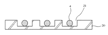
<工程(A)>
図2Aに示すように、開口21が形成された転写型20の開口21内に導電粒子4を配置し、図2Bに示すように、開口21が形成された転写型20の表面に、剥離フィルム22上に形成された絶縁性樹脂層10を対向させる。
<Process (A)>
As shown in FIG. 2A, the
転写型20としては、例えば、シリコン、各種セラミックス、ガラス、ステンレススチールなどの金属等の無機材料や、各種樹脂等の有機材料などに対し、フォトリソグラフ法等の公知の開口形成方法によって開口を形成したものである。このような転写型20は、板状、ロール状等の形状をとることができる。
As the
転写型20の開口21は、その内部に導電粒子4を収容するものである。開口21の形状としては、円柱状、四角錐等の多角柱状、四角錐等の角錐状等を例示することができる。
The
開口21の配列としては、格子状、千鳥状等の規則的な配列とすることが好ましい。
The arrangement of the
なお、転写型20の開口21の径と深さは、レーザー顕微鏡で測定することができる。
The diameter and depth of the
転写型20の開口21内に導電粒子4を収容する手法としては、特に限定されるものではなく、公知の手法を採用することができる。例えば、乾燥した導電粒子粉末またはこれを溶媒中に分散させた分散液を転写型20の開口形成面上に散布または塗布した後、ブラシやブレードなどを用いて開口形成面の表面をワイプすればよい。
The method for accommodating the
開口21の深さに対する導電粒子4の平均粒径の比(=導電粒子の平均粒径/開口の深さ)は、転写性向上と導電粒子保持性とのバランスから、好ましくは0.4〜3.0、より好ましくは0.5〜1.5である。
The ratio of the average particle diameter of the
また、開口21の径の導電粒子4の平均粒径に対する比(=開口の径/導電粒子の平均粒径)は、導電粒子の収容のしやすさ、絶縁性樹脂の押し込みやすさ等のバランスから、好ましくは1.1〜2.0、より好ましくは1.3〜1.8である。
The ratio of the diameter of the
なお、開口21の径よりもその基底側が径が小さい場合には、基底径は導電粒子径の1.1倍以上2倍未満とし、開口径を導電粒子径の1.3倍以上3倍未満とすることが好ましい。
When the diameter of the base side is smaller than the diameter of the
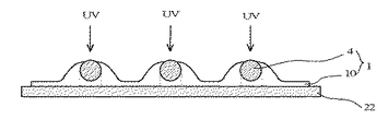
<工程(B)>
次に、図3Aに示すように、剥離フィルム22側から絶縁性樹脂層10に対して圧力をかけ、開口21内に絶縁性樹脂を押し込んで絶縁性樹脂層10の表面に導電粒子4を埋め込むように転着させる。これにより、図3Bに示すような、絶縁性樹脂層10の平面方向に導電粒子4が単層で配列された構造であって、隣接する導電粒子4間の中央領域の絶縁性樹脂層厚が、導電粒子近傍の絶縁性樹脂層厚よりも薄くなっている第1接続層1を形成する。この場合、隣接する導電粒子4間で絶縁性樹脂層厚が実施的に0となってもよい(図1C参照)。実質的に0になると、接続後の個々の導電粒子の独立性が高まり、接続時に導電粒子が互いに連結することを防止し易くなる。
<Process (B)>
Next, as shown in FIG. 3A, pressure is applied to the insulating
<工程(C)>
次に、図4に示すように、第1接続層1の導電粒子4側表面に、主として絶縁性樹脂からなる第2接続層2を形成する。これにより、第1接続層と第2接続層の境界が起伏した状態、換言すればその形状が波型ないしは凹凸型となる。このように、フィルム内に存在する層に起伏のある形状を適用することで、接合時の主にバンプに対しての接触面積を増加させる確率を高めることができ、その結果、接着強度の向上が期待できる。
<Process (C)>
Next, as shown in FIG. 4, the
<工程(D)>
次に、剥離フィルム22を取り除いたのち、第2接続層2と反対側の第1接続層1の表面に、主として絶縁性樹脂からなる第3接続層3を形成する。これにより、図5に示す異方性導電フィルム100が得られる。
<Process (D)>
Next, after removing the
なお、工程(B)と工程(C)との間に、図3Cに示すように、第1接続層1に対し、導電粒子4側から紫外線UVを照射することが好ましい。これにより、導電粒子4を第1接続層1に固定化でき、しかも、導電粒子4の下方の第1接続層1の硬化率をその周囲に比べ相対的に低くすることができ、異方性導電接続の際の導電粒子の押し込み性を向上させることができる。
In addition, it is preferable to irradiate the ultraviolet rays UV from the
<<異方性導電フィルムの製造方法>>
また、本発明の異方性導電フィルムの別の製造方法の例を説明する。この製造方法は、剥離フィルム22に代えて第3接続層3を使用する態様であり、以下の工程(a)〜(c)を有する。以下工程毎に説明する。
<< Method for Manufacturing Anisotropic Conductive Film >>
Moreover, the example of another manufacturing method of the anisotropic conductive film of this invention is demonstrated. This manufacturing method is an embodiment in which the
<工程(a)>
図6Aに示すように、開口21が形成された転写型20の開口21内に導電粒子4を配置し、図6Bに示すように、開口21が形成された転写型20の表面に、予め第3接続層3が貼り合わされた絶縁性樹脂層10を対向させる。
<Process (a)>
As shown in FIG. 6A, the
<工程(b)>
次に、図7Aに示すように、第3接続層3側から絶縁性樹脂層10に対して圧力をかけ、開口21内に絶縁性樹脂を押し込んで絶縁性樹脂層10の表面に導電粒子4を転着させる。これにより、図7Bに示すような、絶縁性樹脂層10の平面方向に導電粒子4が単層で配列された構造であって、隣接する導電粒子4間の中央領域の絶縁性樹脂層厚が、導電粒子近傍の絶縁性樹脂層厚よりも薄くなっている第1接続層1を形成する。この場合、隣接する導電粒子4間で絶縁性樹脂層厚が実施的に0となってもよい(図1C参照)。実質的に0になると、接続後の個々の導電粒子の独立性が高まり、接続時に導電粒子が互いに連結することを防止し易くなる。
<Step (b)>
Next, as shown in FIG. 7A, pressure is applied to the insulating
<工程(c)>
次に、第1接続層1の導電粒子4側表面に、主として絶縁性樹脂からなる第2接続層2を形成する。これにより、図8に示す異方性導電フィルム100が得られる。
<Step (c)>
Next, the
なお、工程(b)と工程(c)との間に、図7Cに示すように、第1接続層1に対し、導電粒子4側から紫外線UVを照射することが好ましい。これにより、導電粒子4を第1接続層1に固定化でき、しかも、導電粒子4の下方の第1接続層1の硬化率をその周囲に比べ相対的に低くすることができ、異方性導電接続の際の導電粒子の押し込み性を向上させることができる。
In addition, it is preferable to irradiate the ultraviolet rays UV from the
ところで、図8に示す異方性導電フィルムにおいては、導電粒子4は第1接続層1に主に包含されている。この場合、一つの導電粒子についてみたときに、それを包み込んでいる第1接続層1の領域は第2接続層2側に凸形状となっており、従って、その領域の第2接続層側の幅よりも、第3接続層側の幅が広くなっている。この幅の広い側における導電粒子4の厚み方向端部(粒子の下側端部)と第2接続層2までの水平方向の最短距離pが、接続時の導電粒子の安定性に寄与する。即ち、pは固定部分の台座に相当する役割を有する。換言すれば、導電粒子近傍の樹脂が山型になることは、これに包含されている粒子をその内部に留めさせ、孤立化させる。これは、押圧によって導電粒子が圧縮される際、その導電粒子を包み込んでいる第1接続層の裾野部分の存在によって平面方向への導電粒子の流動は相対的に抑制される確率が高まるからである。この効果は、既に説明したように、導電粒子間中央領域に第1接続層の厚みが存在しなくても、本質的には同様の効果を示す。これは、上記したように粒子流動の抑制はその近傍樹脂の形状で担うためであり、その端部が閉鎖的であるか、わずかに開放的であるかには、本質的な差異はないためである。このため、導電粒子間の連結を防止するという効果としては、結果として略同一の発現が期待できる。以上のことから、pは山型の裾野までに相当する長さ、つまり作用効果が期待できるまでの長さを表す。この場合、導電粒子の厚み方向端部と第2接続層2までの水平方向の最短距離pは、好ましくは導電粒子径の0.5〜1.5倍、より好ましくは0.55〜1.25倍となる。
By the way, in the anisotropic conductive film shown in FIG. 8, the
<<異方性導電フィルムの用途>>
このようにして得られた異方性導電フィルムは、ICチップ、ICモジュールなどの第1電子部品と、フレキシブル基板、ガラス基板などの第2電子部品とを熱又は光により異方性導電接続する際に好ましく適用することができる。このようにして得られる接続構造体も本発明の一部である。この場合、配線基板などの第2電子部品に対し、異方性導電フィルムをその第3接続層側から仮貼りし、仮貼りされた異方性導電フィルムに対し、ICチップなどの第1電子部品を搭載し、第1電子部品側から熱圧着することが、接続信頼性を高める点から好ましい。また、光硬化を利用して接続することもできる。
<< Use of anisotropic conductive film >>
The anisotropic conductive film thus obtained connects the first electronic component such as an IC chip or IC module and the second electronic component such as a flexible substrate or a glass substrate by heat or light. In particular, it can be preferably applied. The connection structure thus obtained is also part of the present invention. In this case, an anisotropic conductive film is temporarily attached to the second electronic component such as a wiring board from the third connection layer side, and the first electronic such as an IC chip is attached to the temporarily attached anisotropic conductive film. It is preferable from the viewpoint of improving connection reliability that components are mounted and thermocompression bonded from the first electronic component side. Moreover, it can also connect using photocuring.
以下、本発明を実施例により具体的に説明する。 Hereinafter, the present invention will be specifically described by way of examples.
実施例1〜10
表1又は表2に記載された配合に従って、アクリレート及び光ラジカル重合開始剤等を酢酸エチル又はトルエンにて固形分が50質量%となるように混合液を調製した。この混合液を、厚さ50μmのポリエチレンテレフタレートフィルム(PETフィルム)に、乾燥厚が5μmとなるように塗布し、80℃のオーブン中で5分間乾燥することにより、第1接続層となる光ラジカル重合型の絶縁性樹脂層を形成した。
Examples 1-10
According to the composition described in Table 1 or Table 2, a mixed solution of acrylate, photo radical polymerization initiator and the like was prepared with ethyl acetate or toluene so that the solid content was 50% by mass. This mixed solution is applied to a polyethylene terephthalate film (PET film) having a thickness of 50 μm so as to have a dry thickness of 5 μm, and is dried in an oven at 80 ° C. for 5 minutes. A polymerization type insulating resin layer was formed.
次に、直径5.5μmで深さ4.5μmの円柱状の開口が縦横9μmピッチで設けられているステンレススチール製の転写型を用意し、各開口に平均粒径4μmの導電粒子(Ni/Auメッキ樹脂粒子、AUL704、積水化学工業(株))を一つずつ収容した。この転写型の開口形成面に対し、第1接続層用の絶縁性樹脂層を対向させ、剥離フィルム側から、60℃で0.5MPaという条件で加圧することにより導電粒子を絶縁性樹脂層に押し込んだ。これにより、隣接する導電粒子間の中央領域の絶縁性樹脂層厚が、導電粒子近傍の絶縁性樹脂層厚よりも薄くなっている絶縁性樹脂層を形成した。 Next, a transfer mold made of stainless steel in which cylindrical openings having a diameter of 5.5 μm and a depth of 4.5 μm are provided at a pitch of 9 μm in length and width is prepared, and conductive particles (Ni / Ni) having an average particle diameter of 4 μm are prepared in each opening. Au plated resin particles, AUL704, Sekisui Chemical Co., Ltd.) were accommodated one by one. The insulating resin layer for the first connection layer is opposed to the opening forming surface of the transfer mold, and the conductive particles are applied to the insulating resin layer by pressing from the release film side under the condition of 0.5 MPa at 60 ° C. I pushed it in. As a result, an insulating resin layer in which the insulating resin layer thickness in the central region between adjacent conductive particles is thinner than the insulating resin layer thickness in the vicinity of the conductive particles was formed.
次に、この導電粒子側から光ラジカル重合型の絶縁性樹脂層に対し、波長365nm、積算光量4000mL/cm2の紫外線を照射することにより、表面に導電粒子が固定された第1接続層を形成した。 Next, by irradiating the photo radical polymerization type insulating resin layer from the conductive particle side with ultraviolet rays having a wavelength of 365 nm and an integrated light amount of 4000 mL / cm 2 , a first connection layer having conductive particles fixed on the surface is formed. Formed.
熱硬化性樹脂及び潜在性硬化剤等を酢酸エチル又はトルエンにて固形分が50質量%となるように混合液を調製した。この混合液を、厚さ50μmのPETフィルムに、乾燥厚が12μmとなるように塗布し、80℃のオーブン中で5分間乾燥することにより、第2接続層とを形成した。同様の操作により乾燥厚3μmの第3接続層を形成した。 A liquid mixture of a thermosetting resin and a latent curing agent was prepared with ethyl acetate or toluene so that the solid content was 50% by mass. This mixed solution was applied to a PET film having a thickness of 50 μm so as to have a dry thickness of 12 μm, and dried in an oven at 80 ° C. for 5 minutes to form a second connection layer. A third connection layer having a dry thickness of 3 μm was formed by the same operation.
このようにして得られた第1接続層に、第2接続層を、導電粒子が内側となるように、60℃、0.5MPaという条件でラミネートし、続いて反対面に第3接続層を同様にラミネートすることにより異方性導電フィルムを得た。 The second connection layer was laminated to the first connection layer thus obtained under the conditions of 60 ° C. and 0.5 MPa so that the conductive particles were inside, and then the third connection layer was formed on the opposite surface. The anisotropic conductive film was obtained by laminating similarly.
なお、実施例7〜10については、導電粒子間の第1接続層の厚みが実質的に0となるように異方性導電フィルムを作成した。具体的には、第1接続層用の絶縁性樹脂層を対向させ、剥離フィルム側から、60℃で0.5MPaという条件で加圧した後、60℃で1.0MPaという条件で再加圧すること以外は、実施例1と同様の条件で異方性導電フィルムを作成した。 In addition, about Examples 7-10, the anisotropic conductive film was created so that the thickness of the 1st connection layer between electroconductive particles might be set to 0 substantially. Specifically, the insulating resin layer for the first connection layer is made to face, and after pressurizing from the release film side under the condition of 0.5 MPa at 60 ° C., it is re-pressurized under the condition of 1.0 MPa at 60 ° C. Except for this, an anisotropic conductive film was prepared under the same conditions as in Example 1.
比較例1
表1に記載された配合に従って、実施例1と同様に第1接続層の前駆層である光ラジカル重合型の絶縁性樹脂層を形成した。
Comparative Example 1
According to the formulation described in Table 1, a photo-radical polymerization type insulating resin layer, which is a precursor layer of the first connection layer, was formed in the same manner as in Example 1.
次に、直径5.5μmで深さ4.5μmの円柱状の開口が縦横9μmピッチで設けられているステンレススチール製の転写型を用意し、各開口に平均粒径4μmの導電粒子(Ni/Auメッキ樹脂粒子、AUL704、積水化学工業(株))を一つずつ収容した。この転写型の開口形成面に対し、第1接続層用の絶縁性樹脂層を対向させ、剥離フィルム側から、40℃で0.1MPaという相対的に弱い条件で加圧することにより導電粒子を絶縁性樹脂層表面に転写した。導電粒子が転写されたこのフィルムを取り出し、導電粒子を絶縁性樹脂層中に、樹脂層の表面が平坦となるように完全に押し込んだ。 Next, a transfer mold made of stainless steel in which cylindrical openings having a diameter of 5.5 μm and a depth of 4.5 μm are provided at a pitch of 9 μm in length and width is prepared, and conductive particles (Ni / Ni) having an average particle diameter of 4 μm are prepared in each opening. Au plated resin particles, AUL704, Sekisui Chemical Co., Ltd.) were accommodated one by one. The insulating resin layer for the first connection layer is opposed to the opening forming surface of the transfer mold, and the conductive particles are insulated by pressing from the release film side at a relatively weak condition of 0.1 MPa at 40 ° C. Was transferred to the surface of the conductive resin layer. The film on which the conductive particles were transferred was taken out, and the conductive particles were completely pushed into the insulating resin layer so that the surface of the resin layer was flat.
次に、導電粒子が埋め込まれた光ラジカル重合型の絶縁性樹脂層に対し、波長365nm、積算光量4000mL/cm2の紫外線を照射することにより平坦な第1接続層を形成した。 Next, a flat first connection layer was formed by irradiating ultraviolet light having a wavelength of 365 nm and an integrated light amount of 4000 mL / cm 2 to the photo radical polymerization type insulating resin layer in which the conductive particles were embedded.
この第1接続層に対し、実施例1と同様に作成した12μm厚の第2接続層と3μm厚の第3接続層とをラミネートすることにより異方性導電フィルムを得た。 An anisotropic conductive film was obtained by laminating a 12 μm-thick second connection layer and a 3 μm-thick third connection layer prepared in the same manner as in Example 1 on the first connection layer.
比較例2
表1の第1接続層用の樹脂組成物に実施例1で使用したものと同じ導電粒子を1平方mm当たり20000個となるように均一に分散した混合物から、厚さ6μmの導電粒子含有樹脂フィルムを作成した。このフィルムに対し、実施例1と同様に作成した厚さ12μmの第2接続層を、60℃で0.5MPaという条件で貼り付けることにより2層構造の異方性導電フィルムを作成した。
Comparative Example 2
A conductive particle-containing resin having a thickness of 6 μm is obtained from a mixture in which the same conductive particles as used in Example 1 in the resin composition for the first connection layer shown in Table 1 are uniformly dispersed so as to have 20000 per square mm. A film was created. An anisotropic conductive film having a two-layer structure was prepared by sticking a 12 μm-thick second connection layer prepared in the same manner as in Example 1 to this film under the condition of 0.5 MPa at 60 ° C.
<評価>
得られた異方性導電フィルムにおける導電粒子間の平面方向均等配列について、平面均等配列が形成されている場合にはその適用があり(有)とし、それ以外を適用なし(無)とする。また、導電粒子近傍の絶縁性樹脂層厚について、導電粒子間の中間領域の絶縁性樹脂層厚(層厚0も含む)よりも大きい場合には、導電粒子近傍の絶縁性樹脂層厚の増大があり(有)とし、それ以外の場合をなし(無)とした。その結果を表1又は表2に示す。なお、異方性導電フィルムの構成層数も併せて示す。
<Evaluation>
Regarding the uniform arrangement in the plane direction between the conductive particles in the obtained anisotropic conductive film, the flat uniform arrangement is applied (yes), and the others are not applicable (no). Further, if the insulating resin layer thickness near the conductive particles is larger than the insulating resin layer thickness (including the layer thickness 0) in the intermediate region between the conductive particles, the insulating resin layer thickness near the conductive particles is increased. There was (Yes), and no (No) in other cases. The results are shown in Table 1 or Table 2. The number of constituent layers of the anisotropic conductive film is also shown.
得られた異方性導電フィルムを用いて、0.5×1.8×20.0mmの大きさのICチップ(バンプサイズ30×85μm:バンプ高さ15μm、バンプピッチ50μm)を、0.5×50×30mmの大きさのコーニング社製のガラス配線基板(1737F)に180℃、80MPa、5秒という条件で実装して接続構造サンプル体を得た。この接続構造サンプル体の接続部の断面を電子顕微鏡で観察したところ、図1Aに示したように、導電粒子の周囲に絶縁性樹脂層が存在していることが確認できた。 Using the obtained anisotropic conductive film, an IC chip (bump size 30 × 85 μm: bump height 15 μm, bump pitch 50 μm) of 0.5 × 1.8 × 20.0 mm is 0.5 The sample was mounted on a glass wiring board (1737F) manufactured by Corning having a size of × 50 × 30 mm under the conditions of 180 ° C., 80 MPa, and 5 seconds to obtain a connection structure sample body. When the cross section of the connection portion of the connection structure sample was observed with an electron microscope, it was confirmed that an insulating resin layer was present around the conductive particles as shown in FIG. 1A.
得られた接続構造サンプル体について、以下に説明するように、「最低溶融粘度」、「粒子捕捉効率」、「導通信頼性」及び「絶縁性」を試験評価した。得られた結果を表1又は表2に示す。 The obtained connection structure sample was tested and evaluated for “minimum melt viscosity”, “particle trapping efficiency”, “conduction reliability”, and “insulation” as described below. The obtained results are shown in Table 1 or Table 2.
「最低溶融粘度」
接続構造サンプル体を構成する第1接続層及び第2接続層のそれぞれの最低溶融粘度を、回転式レオメータ(TA Instruments社)を用い、昇温速度10℃/分;測定圧力5g一定;使用測定プレート直径8mmという条件で測定した。
"Minimum melt viscosity"
The minimum melt viscosity of each of the first connection layer and the second connection layer constituting the connection structure sample body was measured using a rotary rheometer (TA Instruments) at a heating rate of 10 ° C./min; Measurement was performed under the condition of a plate diameter of 8 mm.
「粒子捕捉効率」
“加熱・加圧前の接続構造サンプル体のバンプ上に存在する理論粒子量”に対する“加熱・加圧後(実際の実装後)の接続構造サンプル体のバンプ上で実際に捕捉されている粒子量”の割合を以下の数式に従って求めた。実用上、50%以上であることが望ましい。
"Particle capture efficiency"
Particles that are actually trapped on the bumps of the connection structure sample body after heating / pressurization (after actual mounting) against the “theoretical particle amount existing on the bumps of the connection structure sample body before heating / pressurization” The ratio of “amount” was determined according to the following formula. Practically, it is desirable that it is 50% or more.
![]()
![]()
「導通信頼性」
接続構造サンプル体を、85℃、85%RHの高温高湿環境下に放置し、初期と500時間経過後の導通抵抗値を測定した。実用上、500時間経過後でも抵抗値10Ω以下であることが望ましい。
"Conduction reliability"
The connection structure sample was left in a high-temperature and high-humidity environment at 85 ° C. and 85% RH, and the conduction resistance value at the initial stage and after the elapse of 500 hours was measured. Practically, it is desirable that the resistance value is 10Ω or less even after 500 hours.
「絶縁性」
7.5μmスペースの櫛歯TEGパターンのショート発生率を求めた。実用上、100ppm以下であることが望ましい。
"Insulation"
The short-circuit occurrence rate of the comb tooth TEG pattern in the 7.5 μm space was determined. Practically, it is desirably 100 ppm or less.

表1から分かるように、実施例1〜6の異方性導電フィルムについては、粒子捕捉効率、導通信頼性、絶縁性の各評価項目についてはいずれも実用上好ましい結果を示した。なお、実施例1〜4の結果から、第1、第2、第3接続層がいずれも同じ硬化系であると、それらの層同士が反応するので、導電粒子の押し込み性が若干低下して導通抵抗値が上昇する傾向があることがわかる。また、第1接続層がカチオン重合系であると、ラジカル重合系よりも耐熱性が改善されるので、やはり導電粒子の押し込み性が若干低下して導通抵抗値が上昇する傾向があることがわかる。 As can be seen from Table 1, the anisotropic conductive films of Examples 1 to 6 showed practically preferable results for the evaluation items of particle trapping efficiency, conduction reliability, and insulation. In addition, from the results of Examples 1 to 4, when the first, second, and third connection layers are all the same curing system, the layers react with each other, so the pushability of the conductive particles is slightly reduced. It can be seen that the conduction resistance value tends to increase. In addition, when the first connection layer is a cationic polymerization system, the heat resistance is improved as compared with the radical polymerization system, so that it is understood that the pushability of the conductive particles also slightly decreases and the conduction resistance value tends to increase. .
それに対し、比較例1の異方性導電フィルムについては、第1接続層において、隣接する導電粒子間の中央領域の絶縁性樹脂層厚が、導電粒子近傍の絶縁性樹脂層厚よりも薄くなっていないので、導通信頼性が大きく低下してしまった。従来の2層構造の比較例2の異方性導電フィルムについては、粒子捕捉効率が大きく低下し、絶縁性にも問題があった。 In contrast, in the anisotropic conductive film of Comparative Example 1, in the first connection layer, the insulating resin layer thickness in the central region between adjacent conductive particles is thinner than the insulating resin layer thickness in the vicinity of the conductive particles. As a result, the conduction reliability has greatly deteriorated. About the anisotropic conductive film of the comparative example 2 of the conventional 2 layer structure, particle | grain capture efficiency fell greatly and there existed a problem also in insulation.
また、表2からわかるように、実施例7〜10の異方性導電フィルムは、導電粒子間中央部の厚みがゼロであるため導電粒子の独立性が高まり、粒子捕捉効率、導通信頼性、絶縁性の各評価項目についてはいずれも実用上好ましい結果を示した。 Further, as can be seen from Table 2, the anisotropic conductive films of Examples 7 to 10 have an independence of the conductive particles because the thickness of the central portion between the conductive particles is zero, and the particle trapping efficiency, conduction reliability, For each of the evaluation items of insulating properties, practically preferable results were shown.
第1接続層が絶縁性の第2接続層と第3接続層とに挟持された3層構造の本発明の異方性導電フィルムは、第1接続層が、絶縁性樹脂層の第2接続層側の平面方向に導電粒子が単層で配列された構造を有し、隣接する導電粒子間の中央の絶縁性樹脂層厚が、導電粒子近傍の絶縁性樹脂層厚よりも薄くなっている構造を有する。このため、導電粒子が単層で配列された異方性導電フィルムにおいて、良好な接続信頼性、良好な絶縁性、及び良好な粒子捕捉効率を実現できる。よって、ICチップなどの電子部品の配線基板への異方性導電接続に有用である。 In the anisotropic conductive film of the present invention having a three-layer structure in which the first connection layer is sandwiched between the insulating second connection layer and the third connection layer, the first connection layer is the second connection of the insulating resin layer. It has a structure in which conductive particles are arranged in a single layer in the plane direction on the layer side, and the insulating resin layer thickness at the center between adjacent conductive particles is thinner than the insulating resin layer thickness near the conductive particles It has a structure. For this reason, in the anisotropic conductive film in which the conductive particles are arranged in a single layer, it is possible to realize good connection reliability, good insulation, and good particle capturing efficiency. Therefore, it is useful for anisotropic conductive connection of an electronic component such as an IC chip to a wiring board.
1 第1接続層
1X 第1接続層における硬化率の低い領域
1Y 第1接続層における硬化率の高い領域
1d 被覆層
2 第2接続層
3 第3接続層
3a 第3接続層の表面
4 導電粒子
10 絶縁性樹脂層
20 転写型
21 開口
22 剥離フィルム
100 異方性導電フィルム
L 導電粒子間距離
P 導電粒子間距離の中間点
t1、t2 絶縁性樹脂層厚
DESCRIPTION OF
Claims (16)
第1接続層が、絶縁性樹脂層の第2接続層側の平面方向に導電粒子が単層で配列された構造を有し、隣接する導電粒子間の中央領域の絶縁性樹脂層厚が、導電粒子近傍の絶縁性樹脂層厚よりも薄くなっており、導電粒子が、第2接続層に食い込んでいる異方性導電フィルム。 The first connection layer is an anisotropic conductive film having a three-layer structure sandwiched between a second connection layer and a third connection layer mainly made of an insulating resin,
The first connection layer has a structure in which conductive particles are arranged in a single layer in the planar direction on the second connection layer side of the insulating resin layer, and the insulating resin layer thickness in the central region between adjacent conductive particles is An anisotropic conductive film that is thinner than the thickness of the insulating resin layer in the vicinity of the conductive particles, and the conductive particles bite into the second connection layer .
第1接続層が、絶縁性樹脂層の第2接続層側の平面方向に導電粒子が単層で配列された構造を有し、隣接する導電粒子間の中央領域の絶縁性樹脂層厚が、導電粒子近傍の絶縁性樹脂層厚よりも薄くなっており、
第1接続層において、導電粒子と第1接続層の第3接続層側表面との間に位置する領域の第1接続層の硬化率が、互いに隣接する導電粒子間に位置する領域の第1接続層の硬化率よりも低い異方性導電フィルム。 The first connection layer is an anisotropic conductive film having a three-layer structure sandwiched between a second connection layer and a third connection layer mainly made of an insulating resin,
The first connection layer has a structure in which conductive particles are arranged in a single layer in the planar direction on the second connection layer side of the insulating resin layer, and the insulating resin layer thickness in the central region between adjacent conductive particles is It is thinner than the insulating resin layer thickness near the conductive particles ,
In the first connection layer, the curing rate of the first connection layer in the region located between the conductive particles and the surface of the first connection layer on the third connection layer side is the first in the region located between the adjacent conductive particles. An anisotropic conductive film lower than the curing rate of the connection layer .
第1接続層が、絶縁性樹脂層の第2接続層側の平面方向に導電粒子が単層で配列された構造を有し、隣接する導電粒子間の中央領域の絶縁性樹脂層厚が、導電粒子近傍の絶縁性樹脂層厚よりも薄くなっており、
導電粒子の厚み方向端部と第2接続層までの水平方向の最短距離が、粒子径の0.5〜1.5倍である異方性導電フィルム。 The first connection layer is an anisotropic conductive film having a three-layer structure sandwiched between a second connection layer and a third connection layer mainly made of an insulating resin,
The first connection layer has a structure in which conductive particles are arranged in a single layer in the planar direction on the second connection layer side of the insulating resin layer, and the insulating resin layer thickness in the central region between adjacent conductive particles is It is thinner than the insulating resin layer thickness near the conductive particles ,
An anisotropic conductive film in which the shortest distance in the horizontal direction from the thickness direction end of the conductive particles to the second connection layer is 0.5 to 1.5 times the particle diameter .
第1接続層が、絶縁性樹脂層の第2接続層側の平面方向に導電粒子が単層で配列された構造を有し、隣接する導電粒子間の中央領域の絶縁性樹脂層厚が、導電粒子近傍の絶縁性樹脂層厚よりも薄くなっている異方性導電フィルムの製造方法であって、以下の工程(A)〜(D):
工程(A)
開口が形成された転写型の開口内に導電粒子を配置し、開口が形成された転写型の表面に、剥離フィルム上に形成された絶縁性樹脂層を対向させる工程;
工程(B)
剥離フィルム側から絶縁性樹脂層に対して圧力をかけ、開口内に絶縁性樹脂を押し込んで絶縁性樹脂層の表面に導電粒子を転着させ、それにより、絶縁性樹脂層の平面方向に導電粒子が単層で配列された構造であって、隣接する導電粒子間の中央領域の絶縁性樹脂層厚が、導電粒子近傍の絶縁性樹脂層厚よりも薄くなっている第1接続層を形成する工程;工程(C)
第1接続層の導電粒子側表面に、主として絶縁性樹脂からなる第2接続層を形成する工程; 及び
工程(D)
第2接続層と反対側の第1接続層の表面に、主として絶縁性樹脂からなる第3接続層を形成する工程
を有する製造方法。 The first connection layer is an anisotropic conductive film having a three-layer structure sandwiched between a second connection layer and a third connection layer mainly made of an insulating resin,
The first connection layer has a structure in which conductive particles are arranged in a single layer in the planar direction on the second connection layer side of the insulating resin layer, and the insulating resin layer thickness in the central region between adjacent conductive particles is A method for producing an anisotropic conductive film that is thinner than the thickness of an insulating resin layer in the vicinity of conductive particles , and includes the following steps (A) to (D):
Process (A)
Disposing conductive particles in the opening of the transfer mold in which the opening is formed, and making the insulating resin layer formed on the release film face the surface of the transfer mold in which the opening is formed;
Process (B)
Pressure is applied to the insulating resin layer from the release film side, the insulating resin is pushed into the opening, and the conductive particles are transferred onto the surface of the insulating resin layer, thereby conducting in the plane direction of the insulating resin layer. A structure in which particles are arranged in a single layer, and a first connection layer is formed in which the insulating resin layer thickness in the central region between adjacent conductive particles is thinner than the insulating resin layer thickness in the vicinity of the conductive particles Step (C)
Forming a second connection layer mainly made of an insulating resin on the conductive particle side surface of the first connection layer; and step (D)
The manufacturing method which has the process of forming the 3rd connection layer which consists mainly of insulating resin in the surface of the 1st connection layer on the opposite side to a 2nd connection layer.
第1接続層が、絶縁性樹脂層の第2接続層側の平面方向に導電粒子が単層で配列された構造を有し、隣接する導電粒子間の中央領域の絶縁性樹脂層厚が、導電粒子近傍の絶縁性樹脂層厚よりも薄くなっている異方性導電フィルムの製造方法であって、以下の工程(a)〜(c):<工程(a)>
開口が形成された転写型の開口内に導電粒子を配置し、開口が形成された転写型の表面に、予め第3接続層が貼り合わされた絶縁性樹脂層を対向させる工程;
<工程(b)>
剥離フィルム側から絶縁性樹脂層に対して圧力をかけ、開口内に絶縁性樹脂を押し込んで絶縁性樹脂層の表面に導電粒子を転着させ、それにより、絶縁性樹脂層の平面方向に導電粒子が単層で配列された構造であって、隣接する導電粒子間の中央領域の絶縁性樹脂層厚が、導電粒子近傍の絶縁性樹脂層厚よりも薄くなっている第1接続層を形成する工程;及び
<工程(c)>
第1接続層の導電粒子側表面に、主として絶縁性樹脂からなる第2接続層を形成する工程
を有する製造方法。 The first connection layer is an anisotropic conductive film having a three-layer structure sandwiched between a second connection layer and a third connection layer mainly made of an insulating resin,
The first connection layer has a structure in which conductive particles are arranged in a single layer in the planar direction on the second connection layer side of the insulating resin layer, and the insulating resin layer thickness in the central region between adjacent conductive particles is It is a manufacturing method of the anisotropic conductive film which is thinner than the insulating resin layer thickness in the vicinity of the conductive particles , and includes the following steps (a) to (c): <Step (a)>
Disposing conductive particles in the opening of the transfer mold in which the opening is formed, and facing the insulating resin layer on which the third connection layer is previously bonded to the surface of the transfer mold in which the opening is formed;
<Step (b)>
Pressure is applied to the insulating resin layer from the release film side, the insulating resin is pushed into the opening, and the conductive particles are transferred onto the surface of the insulating resin layer, thereby conducting in the plane direction of the insulating resin layer. A structure in which particles are arranged in a single layer, and a first connection layer is formed in which the insulating resin layer thickness in the central region between adjacent conductive particles is thinner than the insulating resin layer thickness in the vicinity of the conductive particles And <step (c)>
The manufacturing method which has the process of forming the 2nd connection layer which consists mainly of insulating resin in the electroconductive particle side surface of a 1st connection layer.
第2電子部品に対し、異方性導電フィルムをその第3接続層側から仮貼りし、仮貼りされた異方性導電フィルムに対し、第1電子部品を搭載し、第1電子部品側から熱圧着する接続方法。 A claim 1-9 any connection method for connecting anisotropic conductive to the first electronic component a second electronic component in the anisotropic conductive film according to the,
An anisotropic conductive film is temporarily attached to the second electronic component from the third connection layer side, and the first electronic component is mounted on the temporarily attached anisotropic conductive film from the first electronic component side. Connection method for thermocompression bonding.
Priority Applications (1)
| Application Number | Priority Date | Filing Date | Title |
|---|---|---|---|
| JP2013173195A JP6024620B2 (en) | 2012-08-24 | 2013-08-23 | Anisotropic conductive film and manufacturing method thereof |
Applications Claiming Priority (3)
| Application Number | Priority Date | Filing Date | Title |
|---|---|---|---|
| JP2012184833 | 2012-08-24 | ||
| JP2012184833 | 2012-08-24 | ||
| JP2013173195A JP6024620B2 (en) | 2012-08-24 | 2013-08-23 | Anisotropic conductive film and manufacturing method thereof |
Related Child Applications (1)
| Application Number | Title | Priority Date | Filing Date |
|---|---|---|---|
| JP2016201524A Division JP6372543B2 (en) | 2012-08-24 | 2016-10-13 | Anisotropic conductive film and manufacturing method thereof |
Publications (2)
| Publication Number | Publication Date |
|---|---|
| JP2014060150A JP2014060150A (en) | 2014-04-03 |
| JP6024620B2 true JP6024620B2 (en) | 2016-11-16 |
Family
ID=50150047
Family Applications (5)
| Application Number | Title | Priority Date | Filing Date |
|---|---|---|---|
| JP2013173195A Active JP6024620B2 (en) | 2012-08-24 | 2013-08-23 | Anisotropic conductive film and manufacturing method thereof |
| JP2016201524A Active JP6372543B2 (en) | 2012-08-24 | 2016-10-13 | Anisotropic conductive film and manufacturing method thereof |
| JP2018086174A Active JP6840105B2 (en) | 2012-08-24 | 2018-04-27 | Anisotropic conductive film and its manufacturing method |
| JP2019192686A Active JP7024771B2 (en) | 2012-08-24 | 2019-10-23 | Anisotropic conductive film and its manufacturing method |
| JP2021187236A Active JP7315865B2 (en) | 2012-08-24 | 2021-11-17 | Anisotropic conductive film and its manufacturing method |
Family Applications After (4)
| Application Number | Title | Priority Date | Filing Date |
|---|---|---|---|
| JP2016201524A Active JP6372543B2 (en) | 2012-08-24 | 2016-10-13 | Anisotropic conductive film and manufacturing method thereof |
| JP2018086174A Active JP6840105B2 (en) | 2012-08-24 | 2018-04-27 | Anisotropic conductive film and its manufacturing method |
| JP2019192686A Active JP7024771B2 (en) | 2012-08-24 | 2019-10-23 | Anisotropic conductive film and its manufacturing method |
| JP2021187236A Active JP7315865B2 (en) | 2012-08-24 | 2021-11-17 | Anisotropic conductive film and its manufacturing method |
Country Status (7)
| Country | Link |
|---|---|
| US (3) | US20150214176A1 (en) |
| JP (5) | JP6024620B2 (en) |
| KR (4) | KR101716945B1 (en) |
| CN (3) | CN109334132B (en) |
| HK (1) | HK1205366A1 (en) |
| TW (6) | TWI728334B (en) |
| WO (1) | WO2014030744A1 (en) |
Families Citing this family (36)
| Publication number | Priority date | Publication date | Assignee | Title |
|---|---|---|---|---|
| CN104541416B (en) | 2012-08-24 | 2017-07-04 | 迪睿合电子材料有限公司 | The manufacture method and anisotropic conductive film of anisotropic conductive film |
| KR101716945B1 (en) | 2012-08-24 | 2017-03-15 | 데쿠세리아루즈 가부시키가이샤 | Anisotropic conductive film and manufacturing method therefor |
| KR20240025047A (en) * | 2013-11-19 | 2024-02-26 | 데쿠세리아루즈 가부시키가이샤 | Anisotropic electroconductive film and connection structure |
| CN105940564B (en) * | 2014-02-04 | 2020-03-24 | 迪睿合株式会社 | Anisotropic conductive film and method for producing same |
| JP7052254B2 (en) | 2016-11-04 | 2022-04-12 | デクセリアルズ株式会社 | Filler-containing film |
| KR102326117B1 (en) * | 2014-10-28 | 2021-11-15 | 데쿠세리아루즈 가부시키가이샤 | Anisotropic conductive film, manufacturing method for same, and connection structure |
| KR102398451B1 (en) | 2015-01-13 | 2022-05-16 | 데쿠세리아루즈 가부시키가이샤 | Bump-forming film, semiconductor device, manufacturing method thereof, and connection structure |
| SG10201909698RA (en) * | 2015-01-13 | 2019-11-28 | Dexerials Corp | Anisotropic conductive film |
| JP6458503B2 (en) * | 2015-01-13 | 2019-01-30 | デクセリアルズ株式会社 | Anisotropic conductive film, method for producing the same, and connection structure |
| CN107534231B (en) | 2015-05-27 | 2020-04-14 | 迪睿合株式会社 | Anisotropic conductive film and connection structure |
| KR102090450B1 (en) * | 2016-02-15 | 2020-03-18 | 데쿠세리아루즈 가부시키가이샤 | Anisotropic conductive film, its manufacturing method and connecting structure |
| JP2017191688A (en) * | 2016-04-12 | 2017-10-19 | デクセリアルズ株式会社 | Method for inspecting electrical characteristics |
| JP6889020B2 (en) * | 2016-05-02 | 2021-06-18 | デクセリアルズ株式会社 | Manufacturing method of anisotropic conductive film and anisotropic conductive film |
| WO2017191772A1 (en) * | 2016-05-05 | 2017-11-09 | デクセリアルズ株式会社 | Filler alignment film |
| KR20220080204A (en) | 2016-09-13 | 2022-06-14 | 데쿠세리아루즈 가부시키가이샤 | Filler-containing film |
| JP6187665B1 (en) * | 2016-10-18 | 2017-08-30 | デクセリアルズ株式会社 | Anisotropic conductive film |
| CN115710367A (en) * | 2016-10-18 | 2023-02-24 | 迪睿合株式会社 | Filled membranes |
| US20200299474A1 (en) * | 2016-10-18 | 2020-09-24 | Dexerials Corporation | Filler-containing film |
| JP7035370B2 (en) | 2016-10-31 | 2022-03-15 | デクセリアルズ株式会社 | Filler-containing film |
| JP7256351B2 (en) * | 2016-11-30 | 2023-04-12 | デクセリアルズ株式会社 | Conductive particle arrangement film, manufacturing method thereof, inspection probe unit, continuity inspection method |
| JP7039883B2 (en) * | 2016-12-01 | 2022-03-23 | デクセリアルズ株式会社 | Anisotropic conductive film |
| WO2018101106A1 (en) * | 2016-12-01 | 2018-06-07 | デクセリアルズ株式会社 | Anisotropic electroconductive film |
| TWI763750B (en) * | 2016-12-01 | 2022-05-11 | 日商迪睿合股份有限公司 | Anisotropic conductive film |
| US10957462B2 (en) | 2016-12-01 | 2021-03-23 | Dexerials Corporation | Anisotropic conductive film |
| WO2018181694A1 (en) * | 2017-03-30 | 2018-10-04 | 積水化学工業株式会社 | Conductive particles, conductive material, and connection structure |
| CN109273143A (en) * | 2017-07-18 | 2019-01-25 | 玮锋科技股份有限公司 | The production method of anisotropy conductive film |
| JP7066998B2 (en) | 2017-08-23 | 2022-05-16 | デクセリアルズ株式会社 | Spacer-containing tape |
| JP7062389B2 (en) | 2017-08-23 | 2022-05-06 | デクセリアルズ株式会社 | Anisotropic conductive film |
| US20210114147A1 (en) * | 2018-06-26 | 2021-04-22 | Showa Denko Materials Co., Ltd. | Anisotropic conductive film, method for producing same, and method for producing connection structure |
| KR102254467B1 (en) | 2018-07-12 | 2021-05-21 | 에이치엔에스하이텍(주) | Manufacturing method for anisotropic conductive adhesive film |
| CN108882552A (en) * | 2018-08-10 | 2018-11-23 | 武汉华星光电半导体显示技术有限公司 | The bonding method of conducting resinl and circuit board |
| US11240918B2 (en) * | 2018-08-28 | 2022-02-01 | Research And Business Foundation Sungkyunkwan University | Method for flip-chip bonding using anisotropic adhesive polymer |
| KR102238223B1 (en) * | 2018-08-28 | 2021-04-09 | 성균관대학교산학협력단 | A method for flip-chip bonding using anisotropic adhesive polymer |
| CN112017806A (en) * | 2019-05-29 | 2020-12-01 | 玮锋科技股份有限公司 | Conductive film manufacturing method |
| KR20230107273A (en) * | 2020-11-12 | 2023-07-14 | 가부시끼가이샤 레조낙 | Adhesive film for circuit connection and its manufacturing method, and connection structure and its manufacturing method |
| WO2022230638A1 (en) | 2021-04-26 | 2022-11-03 | キヤノン株式会社 | Electrophotographic member, method for producing same, process cartridge, and electrophotographic image-forming device |
Family Cites Families (34)
| Publication number | Priority date | Publication date | Assignee | Title |
|---|---|---|---|---|
| JP3786214B2 (en) * | 1994-05-10 | 2006-06-14 | 日立化成工業株式会社 | Method for producing anisotropic conductive resin film-like molded product |
| US6034331A (en) | 1996-07-23 | 2000-03-07 | Hitachi Chemical Company, Ltd. | Connection sheet and electrode connection structure for electrically interconnecting electrodes facing each other, and method using the connection sheet |
| CN1218439C (en) | 1997-02-27 | 2005-09-07 | 精工爱普生株式会社 | Connecting structure, liquid crystal device, electronic equipment, anisotropic conductive adhesive and method for manufacturing the adhesive |
| JP4289319B2 (en) * | 1997-03-31 | 2009-07-01 | 日立化成工業株式会社 | Circuit connection material, circuit terminal connection structure and connection method |
| JP3678547B2 (en) * | 1997-07-24 | 2005-08-03 | ソニーケミカル株式会社 | Multilayer anisotropic conductive adhesive and method for producing the same |
| JP3491595B2 (en) | 2000-02-25 | 2004-01-26 | ソニーケミカル株式会社 | Anisotropic conductive adhesive film |
| JP3995942B2 (en) * | 2002-01-29 | 2007-10-24 | 旭化成株式会社 | Method for producing conductive adhesive sheet having anisotropy |
| US20030178221A1 (en) | 2002-03-21 | 2003-09-25 | Chiu Cindy Chia-Wen | Anisotropically conductive film |
| JP4130746B2 (en) * | 2002-03-28 | 2008-08-06 | 旭化成エレクトロニクス株式会社 | Conductive adhesive sheet having anisotropy and method for producing the same |
| JP4130747B2 (en) * | 2002-03-28 | 2008-08-06 | 旭化成エレクトロニクス株式会社 | Anisotropic conductive adhesive sheet and manufacturing method thereof |
| CN1906705B (en) | 2004-01-30 | 2010-04-21 | 积水化学工业株式会社 | Conductive fine particle and anisotropic conductive material |
| JP2005235530A (en) * | 2004-02-18 | 2005-09-02 | Hitachi Chem Co Ltd | Circuit connection material |
| JP4385794B2 (en) | 2004-02-26 | 2009-12-16 | ソニーケミカル&インフォメーションデバイス株式会社 | Anisotropic conductive connection method |
| KR100673778B1 (en) | 2005-08-19 | 2007-01-24 | 제일모직주식회사 | Fast curable anisotropic conductive film composition, anisotropic conductive film using the composition and method for fabricating the same |
| KR101240155B1 (en) * | 2006-04-27 | 2013-03-11 | 아사히 가세이 일렉트로닉스 가부시끼가이샤 | Electroconductive particle placement sheet and anisotropic electroconductive film |
| JP4789738B2 (en) | 2006-07-28 | 2011-10-12 | 旭化成イーマテリアルズ株式会社 | Anisotropic conductive film |
| US7923488B2 (en) | 2006-10-16 | 2011-04-12 | Trillion Science, Inc. | Epoxy compositions |
| JP5143449B2 (en) * | 2007-03-02 | 2013-02-13 | 株式会社ダイセル | Thermal or active energy ray curable adhesive |
| EP2001047A1 (en) | 2007-06-07 | 2008-12-10 | Semiconductor Energy Laboratory Co, Ltd. | Semiconductor device |
| CN101849322B (en) * | 2007-09-20 | 2012-07-04 | 索尼化学&信息部件株式会社 | Anisotropic conductive film and its production method, and bonded body employing anisotropic conductive film |
| CN101897245B (en) * | 2007-12-17 | 2013-03-13 | 日立化成工业株式会社 | Circuit connecting material and structure for connecting circuit member |
| JP5549103B2 (en) | 2008-07-11 | 2014-07-16 | デクセリアルズ株式会社 | Anisotropic conductive film |
| JP2010033793A (en) | 2008-07-28 | 2010-02-12 | Tokai Rubber Ind Ltd | Method for manufacturing particle transfer film |
| JP5558140B2 (en) | 2009-06-10 | 2014-07-23 | デクセリアルズ株式会社 | Insulating resin film, joined body using the same, and manufacturing method thereof |
| JP4673933B2 (en) | 2009-08-26 | 2011-04-20 | 積水化学工業株式会社 | Anisotropic conductive material and connection structure |
| JP5400545B2 (en) | 2009-09-25 | 2014-01-29 | 積水化学工業株式会社 | Anisotropic conductive material, connection structure manufacturing method, and connection structure |
| KR101666214B1 (en) * | 2009-11-05 | 2016-10-14 | 삼성디스플레이 주식회사 | Anisotropic conductive film, method of manufacturing the same and display apparatus having the same |
| JP5518747B2 (en) * | 2009-11-16 | 2014-06-11 | 日立化成株式会社 | Circuit connection material and circuit member connection structure using the same |
| JP5565277B2 (en) | 2010-11-09 | 2014-08-06 | デクセリアルズ株式会社 | Anisotropic conductive film |
| KR20170044766A (en) * | 2012-08-01 | 2017-04-25 | 데쿠세리아루즈 가부시키가이샤 | Method for manufacturing anisotropically conductive film, anisotropically conductive film, and connective structure |
| KR101716945B1 (en) * | 2012-08-24 | 2017-03-15 | 데쿠세리아루즈 가부시키가이샤 | Anisotropic conductive film and manufacturing method therefor |
| CN104541416B (en) * | 2012-08-24 | 2017-07-04 | 迪睿合电子材料有限公司 | The manufacture method and anisotropic conductive film of anisotropic conductive film |
| KR20140139902A (en) | 2013-05-28 | 2014-12-08 | 삼성디스플레이 주식회사 | Anisotropic conductive film laminate, display device including the same and method for display device |
| JP2016201405A (en) * | 2015-04-08 | 2016-12-01 | 三菱電機株式会社 | Silicon carbide semiconductor device manufacturing method |
-
2013
- 2013-08-23 KR KR1020147035905A patent/KR101716945B1/en active IP Right Grant
- 2013-08-23 JP JP2013173195A patent/JP6024620B2/en active Active
- 2013-08-23 WO PCT/JP2013/072571 patent/WO2014030744A1/en active Application Filing
- 2013-08-23 TW TW108111322A patent/TWI728334B/en active
- 2013-08-23 TW TW110114138A patent/TWI810551B/en active
- 2013-08-23 TW TW106120898A patent/TWI655084B/en active
- 2013-08-23 TW TW106120899A patent/TWI728136B/en active
- 2013-08-23 TW TW109145247A patent/TWI810505B/en active
- 2013-08-23 KR KR1020177006454A patent/KR102056086B1/en active IP Right Grant
- 2013-08-23 CN CN201810699580.6A patent/CN109334132B/en active Active
- 2013-08-23 CN CN201810699544.XA patent/CN109166649B/en active Active
- 2013-08-23 KR KR1020197036321A patent/KR102345819B1/en active IP Right Grant
- 2013-08-23 KR KR1020217042801A patent/KR102551117B1/en active IP Right Grant
- 2013-08-23 TW TW102130402A patent/TWI651192B/en active
- 2013-08-23 US US14/422,511 patent/US20150214176A1/en not_active Abandoned
- 2013-08-23 CN CN201380044397.8A patent/CN104541411B/en active Active
-
2015
- 2015-06-24 HK HK15105982.2A patent/HK1205366A1/en unknown
-
2016
- 2016-10-13 JP JP2016201524A patent/JP6372543B2/en active Active
-
2018
- 2018-04-27 JP JP2018086174A patent/JP6840105B2/en active Active
-
2019
- 2019-10-23 JP JP2019192686A patent/JP7024771B2/en active Active
- 2019-11-25 US US16/694,212 patent/US11404391B2/en active Active
-
2021
- 2021-11-17 JP JP2021187236A patent/JP7315865B2/en active Active
-
2022
- 2022-05-06 US US17/738,655 patent/US11784154B2/en active Active
Also Published As
Similar Documents
| Publication | Publication Date | Title |
|---|---|---|
| JP6372543B2 (en) | Anisotropic conductive film and manufacturing method thereof | |
| JP7170612B2 (en) | Anisotropic conductive film manufacturing method and anisotropic conductive film | |
| JP6056700B2 (en) | Anisotropic conductive film and manufacturing method thereof |
Legal Events
| Date | Code | Title | Description |
|---|---|---|---|
| A621 | Written request for application examination |
Free format text: JAPANESE INTERMEDIATE CODE: A621 Effective date: 20150701 |
|
| A977 | Report on retrieval |
Free format text: JAPANESE INTERMEDIATE CODE: A971007 Effective date: 20160425 |
|
| A131 | Notification of reasons for refusal |
Free format text: JAPANESE INTERMEDIATE CODE: A131 Effective date: 20160517 |
|
| A521 | Request for written amendment filed |
Free format text: JAPANESE INTERMEDIATE CODE: A523 Effective date: 20160712 |
|
| TRDD | Decision of grant or rejection written | ||
| A01 | Written decision to grant a patent or to grant a registration (utility model) |
Free format text: JAPANESE INTERMEDIATE CODE: A01 Effective date: 20160913 |
|
| A61 | First payment of annual fees (during grant procedure) |
Free format text: JAPANESE INTERMEDIATE CODE: A61 Effective date: 20160926 |
|
| R150 | Certificate of patent or registration of utility model |
Ref document number: 6024620 Country of ref document: JP Free format text: JAPANESE INTERMEDIATE CODE: R150 |
|
| R250 | Receipt of annual fees |
Free format text: JAPANESE INTERMEDIATE CODE: R250 |
|
| R250 | Receipt of annual fees |
Free format text: JAPANESE INTERMEDIATE CODE: R250 |
|
| R250 | Receipt of annual fees |
Free format text: JAPANESE INTERMEDIATE CODE: R250 |
|
| R250 | Receipt of annual fees |
Free format text: JAPANESE INTERMEDIATE CODE: R250 |
|
| R250 | Receipt of annual fees |
Free format text: JAPANESE INTERMEDIATE CODE: R250 |