JP5952425B2 - Electronic component storage container and electronic device - Google Patents
Electronic component storage container and electronic device Download PDFInfo
- Publication number
- JP5952425B2 JP5952425B2 JP2014550095A JP2014550095A JP5952425B2 JP 5952425 B2 JP5952425 B2 JP 5952425B2 JP 2014550095 A JP2014550095 A JP 2014550095A JP 2014550095 A JP2014550095 A JP 2014550095A JP 5952425 B2 JP5952425 B2 JP 5952425B2
- Authority
- JP
- Japan
- Prior art keywords
- insulating member
- electronic component
- pin terminal
- annular member
- component storage
- Prior art date
- Legal status (The legal status is an assumption and is not a legal conclusion. Google has not performed a legal analysis and makes no representation as to the accuracy of the status listed.)
- Active
Links
Images


Classifications
-
- H—ELECTRICITY
- H05—ELECTRIC TECHNIQUES NOT OTHERWISE PROVIDED FOR
- H05K—PRINTED CIRCUITS; CASINGS OR CONSTRUCTIONAL DETAILS OF ELECTRIC APPARATUS; MANUFACTURE OF ASSEMBLAGES OF ELECTRICAL COMPONENTS
- H05K5/00—Casings, cabinets or drawers for electric apparatus
- H05K5/02—Details
- H05K5/0217—Mechanical details of casings
-
- H—ELECTRICITY
- H01—ELECTRIC ELEMENTS
- H01R—ELECTRICALLY-CONDUCTIVE CONNECTIONS; STRUCTURAL ASSOCIATIONS OF A PLURALITY OF MUTUALLY-INSULATED ELECTRICAL CONNECTING ELEMENTS; COUPLING DEVICES; CURRENT COLLECTORS
- H01R13/00—Details of coupling devices of the kinds covered by groups H01R12/70 or H01R24/00 - H01R33/00
- H01R13/40—Securing contact members in or to a base or case; Insulating of contact members
- H01R13/405—Securing in non-demountable manner, e.g. moulding, riveting
-
- H—ELECTRICITY
- H05—ELECTRIC TECHNIQUES NOT OTHERWISE PROVIDED FOR
- H05K—PRINTED CIRCUITS; CASINGS OR CONSTRUCTIONAL DETAILS OF ELECTRIC APPARATUS; MANUFACTURE OF ASSEMBLAGES OF ELECTRICAL COMPONENTS
- H05K5/00—Casings, cabinets or drawers for electric apparatus
- H05K5/06—Hermetically-sealed casings
- H05K5/069—Other details of the casing, e.g. wall structure, passage for a connector, a cable, a shaft
-
- H10W76/60—
-
- H—ELECTRICITY
- H05—ELECTRIC TECHNIQUES NOT OTHERWISE PROVIDED FOR
- H05K—PRINTED CIRCUITS; CASINGS OR CONSTRUCTIONAL DETAILS OF ELECTRIC APPARATUS; MANUFACTURE OF ASSEMBLAGES OF ELECTRICAL COMPONENTS
- H05K2201/00—Indexing scheme relating to printed circuits covered by H05K1/00
- H05K2201/10—Details of components or other objects attached to or integrated in a printed circuit board
- H05K2201/10613—Details of electrical connections of non-printed components, e.g. special leads
- H05K2201/10954—Other details of electrical connections
- H05K2201/10984—Component carrying a connection agent, e.g. solder, adhesive
-
- H—ELECTRICITY
- H05—ELECTRIC TECHNIQUES NOT OTHERWISE PROVIDED FOR
- H05K—PRINTED CIRCUITS; CASINGS OR CONSTRUCTIONAL DETAILS OF ELECTRIC APPARATUS; MANUFACTURE OF ASSEMBLAGES OF ELECTRICAL COMPONENTS
- H05K2201/00—Indexing scheme relating to printed circuits covered by H05K1/00
- H05K2201/10—Details of components or other objects attached to or integrated in a printed circuit board
- H05K2201/10613—Details of electrical connections of non-printed components, e.g. special leads
- H05K2201/10954—Other details of electrical connections
- H05K2201/10992—Using different connection materials, e.g. different solders, for the same connection
-
- H10W76/157—
Landscapes
- Engineering & Computer Science (AREA)
- Microelectronics & Electronic Packaging (AREA)
- Connections Arranged To Contact A Plurality Of Conductors (AREA)
- Semiconductor Lasers (AREA)
- Casings For Electric Apparatus (AREA)
- Physics & Mathematics (AREA)
- Condensed Matter Physics & Semiconductors (AREA)
- General Physics & Mathematics (AREA)
- Computer Hardware Design (AREA)
- Power Engineering (AREA)
Description
本発明は電子部品を収納するための電子部品収納用容器および電子装置に関し、特に電子部品収納用容器の側壁に取り付けられる入出力端子の形状に特徴を有する電子部品収納用容器および電子装置に関するものである。 The present invention relates to an electronic component storage container and electronic device for storing electronic components, and more particularly to an electronic component storage container and electronic device characterized by the shape of an input / output terminal attached to a side wall of the electronic component storage container. It is.
従来の電子部品収納用容器(以下、単に容器またはパッケージともいう)の例を図8に示す。従来のパッケージは、高周波用半導体素子,LD(レーザダイオード),PD(フォトダイオード)等の光半導体素子を収納する。パッケージは、基体101と、基体101の上面に接合された枠体102と、枠体102に取り付けられた入出力端子103とを備えている。
An example of a conventional electronic component storage container (hereinafter also simply referred to as a container or a package) is shown in FIG. A conventional package accommodates an optical semiconductor element such as a high-frequency semiconductor element, an LD (laser diode), or a PD (photodiode). The package includes a
枠体102は、基体101の上側主面に載置部101aを囲繞するように銀(Ag)ロウ等のロウ材で接合される。枠体102は、Fe(鉄)−Ni(ニッケル)−Co(コバルト)合金やFe−Ni合金等の金属材料から形成される。
The
枠体102の一側部には複数の貫通孔102aが形成されている。枠体102の外側には、入出力端子103が接合されている。入出力端子103は、セラミックスから成る平板103aと、平板103aに接合されたピン端子104とから成る。平板103aには、枠体102の貫通孔102aよりも小さい開口を有する複数の貫通穴103bが形成されている。貫通穴103bは、貫通孔102aと同じ間隔で、平板103aの両主面間を貫通するように形成されている。貫通穴103bの開口の周囲にはメタライズ金属層が形成されている。
A plurality of through
そして、複数の貫通穴103bには、複数のピン端子104が、それぞれ複数の貫通穴103bに挿通されて、平板103aのメタライズ金属層にロウ付けされている。ピン端子104は、金属製である。ピン端子104は、貫通穴103bとともに、枠体102の貫通孔102aも挿通して取り付けられる。
A plurality of
ピン端子104は、外部電気回路との高周波信号の入出力を行なう機能を有する。ピン端子104の枠体102の外側の部位は、外部配線にそのままロウ付等で接合される。ピン端子104の枠体102の内側の部位には、電子部品(図示せず)と電気的に接続するためのボンディングワイヤ等が接合される。
The
そして、電子部品は基体101の載置部101aに固定され、電子部品の電極はボンディングワイヤ等を介してピン端子104に接続される。次に、枠体102の上面に蓋体(図示せず)を接合することによって、容器内部に、電子部品を気密に収容する。これによって、最終製品としての電子装置が完成する。
And an electronic component is fixed to the
従来のパッケージにおいて、例えば、ピン端子104の先端にボンディングワイヤ等を接合する際に、ピン端子104の先端に横方向の力が加わり、ピン端子104の平板103aとのロウ付け部にモーメントが加わる。このモーメントによって、ピン端子104のロウ付けが平板103aから外れてしまう場合がある。そして、ピン端子104のロウ付け部において容器の気密性が破れてしまう場合があるという問題があった。
In a conventional package, for example, when a bonding wire or the like is joined to the tip of the
従って、本発明は上記問題点に鑑み完成されたものである。その目的は、入出力端子の取り付け部において接合信頼性を向上し、気密性を保ちやすい電子部品収納用容器および電子装置を提供することにある。 Accordingly, the present invention has been completed in view of the above problems. An object of the present invention is to provide an electronic component storage container and an electronic device that improve the joint reliability at the mounting portion of the input / output terminals and easily maintain airtightness.
本発明の一実施形態に係る電子部品収納用容器は、容器体と、絶縁部材と、ピン端子と、環状部材とを備える。容器体は、底板およびこの底板の中央部を取り囲む側壁から成る。底板および側壁に囲まれた凹部の内側には電子部品が収容される。絶縁部材は、前記側壁に設けられた貫通孔を塞ぐようにしてこの貫通孔の開口の周囲に接合される。ピン端子は、外周面に突出する鍔部を有する。ピン端子は、前記絶縁部材を貫通して前記鍔部が前記絶縁部材に接合される。環状部材は、前記絶縁部材の前記鍔部が接合された面と反対側において、前記ピン端子に通されて前記ピン端子の外周面および前記絶縁部材に接合される。 An electronic component storage container according to an embodiment of the present invention includes a container body, an insulating member, a pin terminal, and an annular member. The container body includes a bottom plate and a side wall that surrounds the central portion of the bottom plate. An electronic component is accommodated inside the recess surrounded by the bottom plate and the side wall. The insulating member is joined around the opening of the through hole so as to close the through hole provided in the side wall. The pin terminal has a flange that protrudes from the outer peripheral surface. The pin terminal penetrates the insulating member and the flange portion is joined to the insulating member. The annular member is passed through the pin terminal and joined to the outer peripheral surface of the pin terminal and the insulating member on the side opposite to the surface where the flange portion of the insulating member is joined.
上記電子部品収納用容器において、前記絶縁部材とこの絶縁部材を貫通している部分の前記ピン端子の外周面との間に空隙を設けてもよい。 In the electronic component housing container, a gap may be provided between the insulating member and an outer peripheral surface of the pin terminal at a portion passing through the insulating member.
また、上記電子部品収納用容器において、前記環状部材の外周の大きさは前記鍔部の外周の大きさよりも小さくされてもよい。 Moreover, the said electronic component storage container WHEREIN: The magnitude | size of the outer periphery of the said annular member may be made smaller than the magnitude | size of the outer periphery of the said collar part.
また、上記電子部品収納用容器において、前記環状部材は前記側壁の前記貫通孔の内側に配置され、前記貫通孔の外側に出ていなくてもよい。 Moreover, the said electronic component storage container WHEREIN: The said annular member is arrange | positioned inside the said through-hole of the said side wall, and does not need to come out to the outer side of the said through-hole.
また、上記電子部品収納用容器において、前記環状部材と前記側壁の前記貫通孔の内面との間に空隙があってもよい。 In the electronic component storage container, a gap may be provided between the annular member and an inner surface of the through hole in the side wall.
また、上記電子部品収納用容器において、前記鍔部と前記絶縁部材とを接合する接合材および前記環状部材と前記絶縁部材とを接合する接合材が、前記絶縁部材内に突き通された前記ピン端子の外周面を経て連続していてもよい。 Further, in the electronic component storage container, the bonding material for bonding the flange portion and the insulating member and the bonding material for bonding the annular member and the insulating member are pierced into the insulating member. You may continue through the outer peripheral surface of a terminal.
また、上記電子部品収納用容器において、前記環状部材は多角形状であり、前記環状部材の角部が前記絶縁部材に接合されていてもよい。 Moreover, the said electronic component storage container WHEREIN: The said annular member is polygonal shape, The corner | angular part of the said annular member may be joined to the said insulating member.
本発明の一実施形態に係る電子装置は、上記いずれかの電子部品収納用容器と、前記凹部の内側に収容され、前記ピン端子に電気的に接続された電子部品とを備えたものである。 An electronic device according to an embodiment of the present invention includes any one of the above-described electronic component storage containers and an electronic component that is accommodated inside the recess and electrically connected to the pin terminal. .
本発明の電子部品収納用容器は、外周面に突出する鍔部を有し、絶縁部材を貫通して鍔部が絶縁部材に接合されたピン端子と、絶縁部材の鍔部が接合された面と反対側において、ピン端子に通されてピン端子の外周面および絶縁部材に接合された環状部材とを備えたものである。ピン端子と絶縁部材との接合強度が向上し、電子部品収納用容器の気密性が向上する。また、ピン端子の先端に力が加わり、絶縁部材との接合部にモーメントが生じても、鍔部が接合された絶縁部材の反対側に環状部材が接合されており、鍔部や環状部材が絶縁部材から剥がれ難い。よって、ピン端子の取付部から気密が破れ難い。 The electronic component storage container of the present invention has a flange portion protruding on the outer peripheral surface, a pin terminal penetrating the insulating member and bonding the flange portion to the insulating member, and a surface where the flange portion of the insulating member is bonded And an annular member that is passed through the pin terminal and joined to the outer peripheral surface of the pin terminal and the insulating member. The bonding strength between the pin terminal and the insulating member is improved, and the air tightness of the electronic component storage container is improved. In addition, even if a force is applied to the tip of the pin terminal and a moment is generated at the joint with the insulating member, the annular member is joined to the opposite side of the insulating member to which the collar is joined. Hard to peel off from insulating member. Therefore, the airtightness is not easily broken from the pin terminal mounting portion.
上記電子部品収納用容器において、絶縁部材とこの絶縁部材を貫通している部分のピン端子の外周面との間に空隙がある場合、ピン端子の外周面と絶縁部材との間の熱膨張差による応力や、その他の応力が生じないようにできる。 In the electronic component storage container, if there is a gap between the insulating member and the outer peripheral surface of the pin terminal in a portion passing through the insulating member, the thermal expansion difference between the outer peripheral surface of the pin terminal and the insulating member It is possible to prevent the occurrence of stress due to or other stresses.
また、環状部材の外周の大きさが鍔部の外周の大きさよりも小さいと、絶縁部材の鍔部が接合された面に鍔部から加えられる力の位置と、その反対側の面で環状部材から加えられる力の位置とが異なることになる。よって、絶縁部材にクラックが生じ難くなる。 In addition, when the size of the outer periphery of the annular member is smaller than the size of the outer periphery of the flange portion, the position of the force applied from the flange portion to the surface where the flange portion of the insulating member is joined and the surface opposite to the annular member The position of the force applied from will be different. Therefore, cracks are less likely to occur in the insulating member.
また、環状部材が側壁の貫通孔の内側に配置され、貫通孔の外側に出ていない場合、側壁の内側に突出するピン端子の先端をすべてボンディングワイヤが接続される領域等に用いることができる。側壁の内側に環状部材を固定する領域を確保する必要が無いので、その分、電子部品収納用容器を小型にすることができる。 Further, when the annular member is disposed inside the through hole of the side wall and does not protrude outside the through hole, the tip of the pin terminal protruding inside the side wall can be used for a region to which the bonding wire is connected. . Since it is not necessary to secure a region for fixing the annular member inside the side wall, the electronic component storage container can be reduced in size accordingly.
また、環状部材と側壁の貫通孔の内面との間に空隙があると、環状部材と側壁との間で熱膨張や熱収縮による応力が生じないようにできる。その結果、絶縁部材にクラックが生じたりすることがなく、電子部品収納用容器の気密性が向上する。 Further, when there is a gap between the annular member and the inner surface of the through hole in the side wall, stress due to thermal expansion or thermal contraction can be prevented from occurring between the annular member and the side wall. As a result, the insulating member is not cracked, and the airtightness of the electronic component storage container is improved.
また、鍔部と絶縁部材とを接合する接合材および環状部材と絶縁部材とを接合する接合材が、絶縁部材内に突き通されたピン端子の外周面を経て連続していると、鍔部と環状部材とを同時に接合可能な生産効率の高いものとできる。 Further, when the bonding material for bonding the flange portion and the insulating member and the bonding material for bonding the annular member and the insulating member are continuous through the outer peripheral surface of the pin terminal penetrated into the insulating member, And the annular member can be joined at the same time with high production efficiency.
また、環状部材が多角形状であり、環状部材の角部が前記絶縁部材に接合されていると、環状部材の辺と絶縁部材との間で気体を流出入させることができ、絶縁部材と鍔部および環状部材によって設けられる空隙が密閉されない。空隙内の気体が膨張・収縮することによって環状部材の接合部に応力が集中することがなく、電子部品収納用容器の気密性を保ちやすくすることができる。 In addition, when the annular member has a polygonal shape and the corners of the annular member are joined to the insulating member, gas can flow in and out between the sides of the annular member and the insulating member. The gap provided by the part and the annular member is not sealed. When the gas in the gap expands and contracts, stress is not concentrated on the joint portion of the annular member, and the airtightness of the electronic component storage container can be easily maintained.
本発明の一実施形態に係る電子装置は、上記いずれかの電子部品収納用容器と、凹部の内側に収容され、ピン端子に電気的に接続された電子部品とを備えたので、ピン端子部分から気密性が破れにくい信頼性の高い電子装置を提供できる。 An electronic device according to an embodiment of the present invention includes any one of the electronic component storage containers described above and an electronic component that is housed inside the recess and electrically connected to the pin terminal. Therefore, it is possible to provide a highly reliable electronic device in which airtightness is not easily broken.
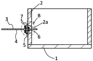
本発明の電子部品収納用容器について以下に詳細に説明する。図1A,図1Bは本発明の電子部品収納用容器の実施の形態の例を示す。図1Aは入出力端子が取り付けられた側から見た斜視図である。図1Bはその裏側から見た斜視図である。また、図2A,図2Bは図1A,図1Bに示すパッケージに用いられている入出力端子の拡大図である。図2Aは入出力端子を図1Aと同じ方向から見た斜視図である。図2Bは入出力端子を図1Bと同じ方向から見た斜視図である。図3は、図2Aの入出力端子の分解斜視図である。図4は、図1A,図1Bの断面A−Aにおける断面図である。 The electronic component storage container of the present invention will be described in detail below. 1A and 1B show an example of an embodiment of an electronic component storage container according to the present invention. FIG. 1A is a perspective view seen from the side where the input / output terminals are attached. FIG. 1B is a perspective view seen from the back side. 2A and 2B are enlarged views of input / output terminals used in the package shown in FIGS. 1A and 1B. 2A is a perspective view of the input / output terminals as viewed from the same direction as FIG. 1A. 2B is a perspective view of the input / output terminals as viewed from the same direction as FIG. 1B. FIG. 3 is an exploded perspective view of the input / output terminal of FIG. 2A. FIG. 4 is a cross-sectional view taken along a cross-section AA in FIGS. 1A and 1B.
図1A,図1Bに示すように、本発明の電子部品収納用容器は容器体を備える。容器体は、底板1と、底板1の中央部を取り囲んで底板外周部に設けられている側壁2とから成る。側壁2には入出力端子3が接合されている。
As shown in FIGS. 1A and 1B, the electronic component storage container of the present invention includes a container body. The container body includes a
底板1は、その上側主面に半導体素子等の電子部品が載置される四角形等の板形状のものである。この底板1は、Fe−Ni−Co合金,Cu(銅)−W(タングステン)等の金属材料、またはAl2O3(酸化アルミニウム),AlN(窒化アルミニウム),3Al2O3・2SiO2(ムライト)等を焼結させたセラミックス(焼結体)から成る。金属材料から成る場合、例えば、Fe−Ni−Co合金のインゴット(塊)に圧延加工や打ち抜き加工等の従来周知の金属加工法を施すことによって所定の形状に製作される。セラミックスから成る場合、その原料粉末に適当な有機バインダや溶剤等を添加混合してペースト状となし、このペーストをドクターブレード法やカレンダーロール法によってセラミックグリーンシートとする。しかる後、セラミックグリーンシートに適当な打ち抜き加工を施し、これを複数枚積層し焼成することによって底板1が作製される。The
なお、底板1が金属材料から成る場合、その表面に耐蝕性に優れかつロウ材との濡れ性に優れる金属、具体的には厚さ0.5〜9μmのNi層と厚さ0.5〜5μmのAu層をメッキ法により順次被着しておくのがよい。底板1を酸化腐蝕し難くするとともに、ロウ付け等の接合性に優れたものとすることができる。一方、底板1がセラミックスから成る場合、電子部品を載置する部分等にメタライズ層を形成しておき、その表面に、厚さ0.5〜9μmのNi層と厚さ0.5〜5μmのAu層をメッキ法により順次被着しておくのがよい。底板1に電子部品等を半田付け等によって強固に接着固定することができる。
When the
図1A,図1Bに示すように、側壁2は、底板1の中央部を囲繞するように取着される。側壁2は、側部に貫通孔2aが形成された平面視形状が四角枠状等の多角形枠状のものである。この側壁2は例えばFe−Ni−Co合金等から成る。Fe−Ni−Co合金のインゴットをプレス加工等により所定の枠状となすことによって製作される。または、底板1と一体に金属インゴットを切削したりして作製してもよい。底板1と側壁2とで囲まれる凹部は、その内側に電子部品を収容する。
As shown in FIGS. 1A and 1B, the
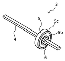
図2A,図2Bに入出力端子3を示す。入出力端子3は、ピン端子4,絶縁部材5,環状部材6を接合して組み立てた組立体である。また、図3は入出力端子の分解斜視図である。これらの図から解るように、入出力端子3は、外周面に鍔部4aを有するピン端子4と、鍔部4aが接合される一方主面およびその裏側の他方主面を有する環状の絶縁部材5と、絶縁部材5の他方主面に取り付けられる環状部材6とから成る。ピン端子4の鍔部4aと環状部材6とは絶縁部材5を間に挟んで絶縁部材5に接合される。環状部材6は絶縁部材5とピン端子4の外周面の両方に接合される。
2A and 2B show the input /
図3に示すように、絶縁部材5は、環状の部材である。絶縁部材5は、両主面間を貫通するように貫通穴5aが形成されたAl2O3,AlN,3Al2O3・2SiO2等を焼結したセラミックス等から成る。貫通穴5aの両面開口の周辺には金属層5bが形成されている。図3では見えていない絶縁部材5の裏面側には、図2Bから判るように、開口周辺の金属層5bとは別に、外周に沿った外側面にも金属層5cが形成されている。図3に示すように、絶縁部材5は円環状で貫通穴5aは円形または楕円形とされる。絶縁部材5の外周および貫通穴5aは多角形状であってもよい。As shown in FIG. 3, the insulating
絶縁部材5は、樹脂やガラス等の絶縁材を成形したものでもよい。なお、金属層5b,5cを形成すると、絶縁部材5にロウ付けによってピン端子4等を接合するのに好適であるが、例えば樹脂接着剤等で接合する場合には必ずしも金属層5b,5cを形成する必要はない。
The insulating
貫通穴5aの内径は、ピン端子4の太さよりも大きいものとしておくとよい。これによって絶縁部材5を貫通しているピン端子4部分と絶縁部材5との間に空隙が設けられる。空隙は、絶縁部材5とピン端子4とを隔てる。したがって、ピン端子4と絶縁部材5との間に熱応力が生じたり、摩擦力が生じたりすることがない。また、空隙部分において、鍔部4aおよび環状部材6は絶縁部材5に接合されない。この接合されない空隙に位置する鍔部4aおよび環状部材6の部分を変形しやすくできるので、ピン端子4に生じるモーメントによる応力を緩和することができる。これにより、ピン端子4の取付部から気密が破れ難いものとすることができる。
The inner diameter of the through
ピン端子4は、例えばFe−Ni−Co合金,Fe−Ni合金,Cu合金,Cu等からなる金属製の棒状部材で、図に示すように四角柱状の他、多角柱状、円柱状等の形状を有する。また、ピン端子4の長さ方向の途中の外周面に鍔部4aが形成されている。鍔部4aは、切削加工や,ヘッダ加工,冷間鍛造等によって所定の形状に製作される。鍔部4aは、絶縁部材5の金属層5bにロウ付け等によって接合される。鍔部4aの形状は、貫通穴5aを塞ぎ、ピン端子4を保持可能な程度の大きさであればよく、円形の他、絶縁部材5の形状と合わせて多角形状としてもよい。なお、ピン端子4の側壁2の内側となる先端部は、ボンディングワイヤ等による接続を容易とするため、平たく潰して形成しておくのが好ましい。ピン端子4は基板上に形成されるメッキ配線等に比べ、大電力信号に対応したものとするのが容易である。
The
環状部材6は、例えばFe−Ni−Co合金,Fe−Ni合金,Cu合金,Cu等からなる金属製の平たい環状のもので、中央にピン端子4を貫通させるための孔6aが設けられている。孔6aはピン端子4の外周面の形状に合わせて設けられる。また、外周面が側壁2の貫通孔2a内に収まる大きさとしておくのがよい。環状部材6の外周の大きさが貫通孔2aの内径より小さいと、環状部材6と貫通孔2aの内面との間に空隙が設けられる。
The
このように、環状部材6が貫通孔2a内に収まる大きさとし、さらに空隙を設けると、環状部材6と側壁2とがそれぞれ熱膨張や熱収縮することに伴って、環状部材6と側壁2との間で熱歪が生じない。その結果、環状部材6と側壁2とに生じる変形が絶縁部材5に影響し、絶縁部材5にクラックが生じたり、絶縁部材5から環状部材6が剥離したりし難くなる。よって、電子部品収納用容器の気密性が向上する。また、側壁2が金属製である場合、空隙によってピン端子4を絶縁することができる。なお、外周の大きさとは、環状部材6または鍔部4aが円形の場合はその直径、楕円形であれば長径、多角形状であればその外接円の直径を意味する。
As described above, when the
環状部材6の外周の大きさは、絶縁部材5の貫通穴5aよりも大きく形成されており、貫通穴5aの開口周囲に接合可能である。しかし、環状部材6の外周の大きさは鍔部4aの外周の大きさよりも小さくしておくのがよい。ピン端子4の先端に力が加わり、絶縁部材5との接合部にモーメントが生じたとき、鍔部4aの外周位置が環状部材6の外周位置よりも外側となり、鍔部4aによるモーメント力および環状部材6によるモーメント力が絶縁部材5の表裏の異なる位置に加わることになる。よって、絶縁部材5に生じる応力が集中しないようにでき、絶縁部材5にクラックを生じ難くすることができる。その結果、電子部品収納用容器の気密性が向上する。
The size of the outer periphery of the
環状部材6が多角形状である場合、図6Aに示すように、環状部材6の角部で絶縁部材5に接合するのがよい。さらに、図6Bに示すように、環状部材6の角と角の間の辺部で空隙5dが形成され、貫通穴5aの開口が環状部材6によって覆われないようにするのがよい。これにより、絶縁部材5と鍔部4aおよび環状部材6によって形成される空間が空隙5dによって開放された状態になるので、空隙内の気体が膨張することによって環状部材6等に圧力が加わることはない。その結果、環状部材6が絶縁部材5から剥がされ難くすることができる。また、ピン端子4および環状部材6を接合する接合材7による気密封止が破れ難くなる。環状部材6は、多角形状である他、アステロイドや内サイクロイド、星型等の角部が外側に突き出した多角形状としてもよい。
When the
また、環状部材6の厚みは、貫通孔2aの長さ、すなわち側壁2の厚みよりも薄いものとするのがよい。これによって、環状部材6は貫通孔2a内に収容され、貫通孔2aの外側に出てこない。したがって、側壁の内側におけるボンディングワイヤの接続作業等に環状部材6が干渉することがない。また、側壁2の内側において環状部材6を固定する領域を確保する必要がない。したがって、その分、側壁2の貫通孔2aの内側に突出するピン端子4の長さを短くできる。その結果、電子部品収納容器は、小型にすることができる。
Further, the thickness of the
そして、ピン端子4を絶縁部材5および環状部材6に通した後に鍔部4aと金属層5bおよび環状部材6と裏面側にある金属層5bとを接合材7を介して接合し、入出力端子3を組み立てる。接合材7として、樹脂接着剤を用いてもよいが、接合力および気密封止性の点で、銀ロウ,銅ロウ,燐銅ロウ等のロウ材7を用いて接合するのがよい。
Then, after passing the
接合は、金属層5bの形状と同様に成形したロウ材のプリフォームを準備し、これを鍔部4aと絶縁部材5および環状部材6と絶縁部材5で挟むように配置した後、所定の温度で加熱、冷却することによって行なわれる。
For the joining, a preform of brazing material formed in the same manner as the shape of the
なお、ロウ付けの際、ロウ材の量および温度を適度に調整することによって、鍔部4aと絶縁部材5とを接合するロウ材7および環状部材6と絶縁部材5とを接合するロウ材7がピン端子4の表面を伝わって流れ、図5に示すように、接合材7がピン端子4の外周面を経て連続し、一体になるようにするのがよい。なお、図5は、入出力端子3の接合部を拡大した断面図で、図4に示すB部に相当する部分の要部拡大図である。これによって、鍔部4aと環状部材6とを絶縁部材5に同時に接合し、生産効率の高い入出力端子3とできる。また、接合力の強いものとできる。
During brazing, the
ピン端子4は、鍔部4aで絶縁部材5に接合される。一方、絶縁部材5の裏面側には環状部材6がピン端子4の外周面および絶縁部材5に接合される。このように、絶縁部材5を鍔部4aおよび環状部材6で挟むように接合しているので、ピン端子4の先端にボンディングワイヤ等を接合処理するとき等に力が加わり、絶縁部材5との接合部にモーメントが生じても、鍔部4aが外れにくくなり、ピン端子4の取付部から気密が破れ難いものとすることができる。
The
入出力端子3を組み立てた後、図1,図4に示すように電子部品収納用容器を組み立てる。ピン端子4の先端を側壁2の貫通孔2aに挿入し、絶縁部材5で貫通孔2aを塞ぐようにして金属層5cをロウ材7によって開口周囲に接合する。側壁2には、取り付けられる入出力端子3と同数の貫通孔2aが設けられており、それぞれの貫通孔2aの開口周囲に入出力端子3の絶縁部材5が接合される。貫通孔2aの形状は、円形,長円形,楕円形,四角形等の多角形、その他種々の形状と為しえるが、絶縁部材5で貫通孔2aを封止可能な形状とされる。絶縁部材5および貫通孔2aを縦長の楕円形または多角形とすることによって、入出力端子3の取付密度を大きくすることができる。
After assembling the input /
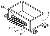
また、図7A,図7Bに示すように、絶縁部材5を複数の貫通穴5aを有する一枚の連続したものとし、それぞれの貫通穴5aにピン端子4および環状部材6を固定した入出力端子3としてもよい。側壁2には、この絶縁部材5を取り付ける一つの大きな貫通孔2aが設けられている。そして、絶縁部材5を、貫通孔2aを塞ぐように、貫通孔2aの開口周囲に接合する。
Further, as shown in FIGS. 7A and 7B, the insulating
このように一枚の絶縁部材5を用いる入出力端子3とすることによって、電子部品収納用容器の組み立て作業を簡略化することができる。さらには、隣接するピン端子4の間に側壁2が介在しないことから、絶縁部材5と側壁2との間で生じる、熱膨張差に起因する応力を抑制することができ、絶縁部材5のクラックを抑制できる。
By using the input /
ピン端子4の側壁2外側の部位は、外部電気回路に半田等で接合され、ピン端子4は電気信号の入出力を行なう機能を担う。半田付けを容易にするため、ピン端子4には、その表面に耐蝕性に優れかつ半田との濡れ性に優れる金属、例えば厚さ0.5〜9μmのNi層と厚さ0.5〜5μmのAu層をメッキ法により順次被着しておくのがよい。その他、底板1や側壁2等の金属部分にも防錆処理として適宜Auメッキ等が施される。
A portion of the
このようにして作製された電子部品収納用容器は、凹部の内側に電子部品が収容され、電子部品の端子とピン端子4の先端とが電気的に接続されることによって、電子装置として機能する。
The electronic component storage container thus manufactured functions as an electronic device by storing the electronic component inside the recess and electrically connecting the terminal of the electronic component and the tip of the
例えば、底板1の上面等に電子部品を接着固定し、電子部品の電極をボンディングワイヤ等を介してピン端子4に接続する。次に、側壁2の上面に側壁2の内側を塞ぐように蓋体を接合し、底板1と側壁2と入出力端子3と蓋体とから成る容器内部に、電子部品を気密に収容する。
For example, an electronic component is bonded and fixed to the upper surface of the
電子部品が光半導体素子等の場合には、側壁2に光ファイバ固定部材を設けておき、ここに光ファイバの一端を挿通させるとともに、これを半田等の接着剤やレーザ溶接によって接合し、光ファイバを側壁2に固定することによって、光半導体素子を収納した光半導体装置となる。
When the electronic component is an optical semiconductor element or the like, an optical fiber fixing member is provided on the
そして、本発明の電子部品収納用容器を用いることにより、気密信頼性が高く、多数の信号を入出力できる入出力端子3を備えた多機能な電子装置となる。
By using the electronic component storage container according to the present invention, a multi-functional electronic device having an airtight reliability and having an input /
なお、本発明は上記実施の形態に限定されるものではなく、本発明の要旨を逸脱しない範囲内であれば種々の変更は可能である。例えば、入出力端子3の絶縁部材5は、ガラスや樹脂等のセラミックス以外の絶縁体から成っていてもよい。
The present invention is not limited to the above-described embodiment, and various modifications can be made without departing from the gist of the present invention. For example, the insulating
また、上記実施形態では入出力端子3を側壁2の外側から接合したが、側壁2の内側に接合してもよい。また、図7に示す入出力端子3において、ピン端子4の鍔部4aを容器の内側になるように接合し、環状部材6を容器の外側に接合してもよい。これにより、容器外側のピン端子の先端を外部電気回路に半田等で接合する際に、ピン端子の先端に力が加わり、絶縁部材との接合部にモーメントが生じても、鍔部が接合された絶縁部材の反対側に環状部材が接合されており、鍔部や環状部材が絶縁部材から剥がれ難い。よって、ピン端子の取付部から気密が破れ難い。
In the above embodiment, the input /
本発明のパッケージは、電子部品として信号処理用の高周波半導体素子、レーザダイオードや受光素子等の光半導体素子、圧電振動子その他各種の電子部品を搭載する電子部品収納用容器として用いることが可能である。 The package of the present invention can be used as an electronic component storage container in which a high-frequency semiconductor element for signal processing, an optical semiconductor element such as a laser diode or a light receiving element, a piezoelectric vibrator, and other various electronic parts are mounted as electronic parts. is there.
1:底板
2:側壁
2a:貫通孔
3:入出力端子
4:ピン端子
4a:鍔部
5:絶縁部材
5a:貫通穴
6:環状部材1: bottom plate 2:
Claims (8)
Applications Claiming Priority (3)
| Application Number | Priority Date | Filing Date | Title |
|---|---|---|---|
| JP2012260567 | 2012-11-29 | ||
| JP2012260567 | 2012-11-29 | ||
| PCT/JP2013/079295 WO2014083992A1 (en) | 2012-11-29 | 2013-10-29 | Electronic component housing package and electronic device |
Publications (2)
| Publication Number | Publication Date |
|---|---|
| JP5952425B2 true JP5952425B2 (en) | 2016-07-13 |
| JPWO2014083992A1 JPWO2014083992A1 (en) | 2017-01-05 |
Family
ID=50827638
Family Applications (1)
| Application Number | Title | Priority Date | Filing Date |
|---|---|---|---|
| JP2014550095A Active JP5952425B2 (en) | 2012-11-29 | 2013-10-29 | Electronic component storage container and electronic device |
Country Status (5)
| Country | Link |
|---|---|
| US (1) | US9516770B2 (en) |
| EP (1) | EP2927949B1 (en) |
| JP (1) | JP5952425B2 (en) |
| CN (1) | CN104396007B (en) |
| WO (1) | WO2014083992A1 (en) |
Families Citing this family (13)
| Publication number | Priority date | Publication date | Assignee | Title |
|---|---|---|---|---|
| US9935025B2 (en) * | 2014-03-13 | 2018-04-03 | Kyocera Corporation | Electronic component housing package and electronic device |
| DE102015223909A1 (en) * | 2015-12-01 | 2017-06-01 | Brose Fahrzeugteile GmbH & Co. Kommanditgesellschaft, Würzburg | System of a first component with a conductor and a partition element and a method of manufacturing the system |
| JP6484588B2 (en) | 2016-05-19 | 2019-03-13 | 日亜化学工業株式会社 | Light emitting device and light emitting device package |
| JP6493308B2 (en) | 2016-05-31 | 2019-04-03 | 日亜化学工業株式会社 | Light emitting device |
| JP6319490B1 (en) * | 2017-03-23 | 2018-05-09 | 住友大阪セメント株式会社 | Light modulator |
| DE102018211293A1 (en) * | 2017-07-10 | 2019-01-10 | Ngk Spark Plug Co., Ltd. | Unit for mounting a light-emitting device |
| JP2019016784A (en) * | 2017-07-10 | 2019-01-31 | 日本特殊陶業株式会社 | Light emitting device mounting package |
| JP6796037B2 (en) * | 2017-07-13 | 2020-12-02 | 本田技研工業株式会社 | Drive circuit unit |
| JP6924641B2 (en) * | 2017-07-17 | 2021-08-25 | 日本特殊陶業株式会社 | Light emitting element mounting package and its manufacturing method |
| WO2020138209A1 (en) * | 2018-12-26 | 2020-07-02 | 京セラ株式会社 | Wiring base, electronic component housing package, and electronic device |
| CN109905995A (en) * | 2019-01-31 | 2019-06-18 | 苏州佳世达光电有限公司 | Proof mechanism of water |
| US10903128B2 (en) * | 2019-02-15 | 2021-01-26 | Microsemi Corporation | Hermetic package for power semiconductor |
| US12046864B2 (en) | 2019-07-25 | 2024-07-23 | Kyocera Corporation | Hermetic terminal |
Citations (5)
| Publication number | Priority date | Publication date | Assignee | Title |
|---|---|---|---|---|
| JPH0897320A (en) * | 1994-09-28 | 1996-04-12 | Shinko Electric Ind Co Ltd | Metal package for electronic parts |
| US5675122A (en) * | 1992-07-27 | 1997-10-07 | Pacific Coast Technologies, Inc. | Sealable electronics packages |
| JP2004228535A (en) * | 2003-01-27 | 2004-08-12 | Kyocera Corp | Semiconductor element storage package and semiconductor device |
| JP2009158673A (en) * | 2007-12-26 | 2009-07-16 | Kyocera Corp | Package and electronic device |
| JP2012248777A (en) * | 2011-05-31 | 2012-12-13 | Kyocera Corp | Package for housing element and semiconductor module including the same |
Family Cites Families (10)
| Publication number | Priority date | Publication date | Assignee | Title |
|---|---|---|---|---|
| US4217137A (en) * | 1978-03-13 | 1980-08-12 | Medtronic, Inc. | Gold based alloy composition and brazing therewith, particularly for ceramic-metal seals in electrical feedthroughs |
| US4338621A (en) * | 1980-02-04 | 1982-07-06 | Burroughs Corporation | Hermetic integrated circuit package for high density high power applications |
| US5093989A (en) * | 1990-11-13 | 1992-03-10 | Frenchtown Ceramics Co. | Method of making heat-resistant hermetic packages for electronic components |
| US5076796A (en) * | 1990-11-19 | 1991-12-31 | Molex Incorporated | Terminal pin for soldering to a printed circuit board |
| US5434358A (en) * | 1993-12-13 | 1995-07-18 | E-Systems, Inc. | High density hermetic electrical feedthroughs |
| JP4058172B2 (en) * | 1997-12-02 | 2008-03-05 | 株式会社住友金属エレクトロデバイス | Optical semiconductor element storage package |
| US6899570B2 (en) * | 2003-05-19 | 2005-05-31 | Eaton Corporation | Hermetically sealed terminal for electrical device |
| JP4373831B2 (en) | 2004-03-26 | 2009-11-25 | 京セラ株式会社 | Electronic component storage package and electronic device |
| JP4817050B2 (en) * | 2006-02-07 | 2011-11-16 | 日立金属株式会社 | Non-reciprocal circuit element |
| DE102008025955B3 (en) * | 2008-05-30 | 2009-12-03 | Concentrix Solar Gmbh | Electric, water vapor diffusion-proof connector |
-
2013
- 2013-10-29 WO PCT/JP2013/079295 patent/WO2014083992A1/en not_active Ceased
- 2013-10-29 EP EP13859529.3A patent/EP2927949B1/en active Active
- 2013-10-29 US US14/416,375 patent/US9516770B2/en active Active
- 2013-10-29 JP JP2014550095A patent/JP5952425B2/en active Active
- 2013-10-29 CN CN201380034691.0A patent/CN104396007B/en active Active
Patent Citations (5)
| Publication number | Priority date | Publication date | Assignee | Title |
|---|---|---|---|---|
| US5675122A (en) * | 1992-07-27 | 1997-10-07 | Pacific Coast Technologies, Inc. | Sealable electronics packages |
| JPH0897320A (en) * | 1994-09-28 | 1996-04-12 | Shinko Electric Ind Co Ltd | Metal package for electronic parts |
| JP2004228535A (en) * | 2003-01-27 | 2004-08-12 | Kyocera Corp | Semiconductor element storage package and semiconductor device |
| JP2009158673A (en) * | 2007-12-26 | 2009-07-16 | Kyocera Corp | Package and electronic device |
| JP2012248777A (en) * | 2011-05-31 | 2012-12-13 | Kyocera Corp | Package for housing element and semiconductor module including the same |
Also Published As
| Publication number | Publication date |
|---|---|
| US20150189775A1 (en) | 2015-07-02 |
| JPWO2014083992A1 (en) | 2017-01-05 |
| EP2927949A1 (en) | 2015-10-07 |
| WO2014083992A1 (en) | 2014-06-05 |
| CN104396007B (en) | 2017-06-13 |
| EP2927949B1 (en) | 2018-08-01 |
| CN104396007A (en) | 2015-03-04 |
| EP2927949A4 (en) | 2016-07-06 |
| US9516770B2 (en) | 2016-12-06 |
Similar Documents
| Publication | Publication Date | Title |
|---|---|---|
| JP5952425B2 (en) | Electronic component storage container and electronic device | |
| JP5902813B2 (en) | Semiconductor element storage package and semiconductor device | |
| JP5981660B2 (en) | Electronic component storage package and electronic device | |
| JP2013074048A (en) | Semiconductor element housing package and semiconductor device | |
| JP4522182B2 (en) | Piezoelectric element storage package, piezoelectric device, and method of manufacturing piezoelectric device | |
| JP5812671B2 (en) | Device storage package and semiconductor device including the same | |
| WO2014119550A1 (en) | Package for housing optical semiconductor element and optical semiconductor device | |
| JP2012248777A (en) | Package for housing element and semiconductor module including the same | |
| JP6034054B2 (en) | Electronic component storage package and electronic device | |
| JP4511376B2 (en) | Connection terminal and electronic component storage package and electronic device using the same | |
| JP4373831B2 (en) | Electronic component storage package and electronic device | |
| JP3642739B2 (en) | Package for storing semiconductor elements | |
| JP2017152557A (en) | Package for housing optical semiconductor element and optical semiconductor device | |
| JP4497762B2 (en) | Optical semiconductor element storage package and optical semiconductor device | |
| JP4511385B2 (en) | Ceramic member joining structure, electronic component storage package and electronic device using the same | |
| JP5528484B2 (en) | Input / output terminal and optical semiconductor element storage package, and optical semiconductor device | |
| JP5725900B2 (en) | Semiconductor element storage package and semiconductor device including the same | |
| JP2014027084A (en) | Package for housing semiconductor element, and semiconductor device | |
| JP2004221327A (en) | Semiconductor element storage package and semiconductor device | |
| JP2005101374A (en) | Semiconductor element storage package and semiconductor device | |
| JP2002164459A (en) | Package for storing semiconductor elements | |
| JP2003309203A (en) | Package for housing semiconductor element and semiconductor device | |
| JP2017069245A (en) | Semiconductor element housing package and semiconductor device | |
| JP2007335422A (en) | Hermetic package and manufacturing method thereof | |
| JP2010177427A (en) | Package for housing optical semiconductor element, and optical semiconductor device |
Legal Events
| Date | Code | Title | Description |
|---|---|---|---|
| TRDD | Decision of grant or rejection written | ||
| A01 | Written decision to grant a patent or to grant a registration (utility model) |
Free format text: JAPANESE INTERMEDIATE CODE: A01 Effective date: 20160510 |
|
| A61 | First payment of annual fees (during grant procedure) |
Free format text: JAPANESE INTERMEDIATE CODE: A61 Effective date: 20160609 |
|
| R150 | Certificate of patent or registration of utility model |
Ref document number: 5952425 Country of ref document: JP Free format text: JAPANESE INTERMEDIATE CODE: R150 |