JP5944022B2 - 磁気抵抗効果センサに利用される二重キャッピング層 - Google Patents
磁気抵抗効果センサに利用される二重キャッピング層 Download PDFInfo
- Publication number
- JP5944022B2 JP5944022B2 JP2015014108A JP2015014108A JP5944022B2 JP 5944022 B2 JP5944022 B2 JP 5944022B2 JP 2015014108 A JP2015014108 A JP 2015014108A JP 2015014108 A JP2015014108 A JP 2015014108A JP 5944022 B2 JP5944022 B2 JP 5944022B2
- Authority
- JP
- Japan
- Prior art keywords
- layer
- magnetic
- disposed
- shield
- read head
- Prior art date
- Legal status (The legal status is an assumption and is not a legal conclusion. Google has not performed a legal analysis and makes no representation as to the accuracy of the status listed.)
- Active
Links
Images


Classifications
-
- G—PHYSICS
- G11—INFORMATION STORAGE
- G11B—INFORMATION STORAGE BASED ON RELATIVE MOVEMENT BETWEEN RECORD CARRIER AND TRANSDUCER
- G11B5/00—Recording by magnetisation or demagnetisation of a record carrier; Reproducing by magnetic means; Record carriers therefor
- G11B5/127—Structure or manufacture of heads, e.g. inductive
- G11B5/33—Structure or manufacture of flux-sensitive heads, i.e. for reproduction only; Combination of such heads with means for recording or erasing only
- G11B5/39—Structure or manufacture of flux-sensitive heads, i.e. for reproduction only; Combination of such heads with means for recording or erasing only using magneto-resistive devices or effects
- G11B5/3903—Structure or manufacture of flux-sensitive heads, i.e. for reproduction only; Combination of such heads with means for recording or erasing only using magneto-resistive devices or effects using magnetic thin film layers or their effects, the films being part of integrated structures
- G11B5/3906—Details related to the use of magnetic thin film layers or to their effects
- G11B5/3916—Arrangements in which the active read-out elements are coupled to the magnetic flux of the track by at least one magnetic thin film flux guide
- G11B5/3919—Arrangements in which the active read-out elements are coupled to the magnetic flux of the track by at least one magnetic thin film flux guide the guide being interposed in the flux path
- G11B5/3922—Arrangements in which the active read-out elements are coupled to the magnetic flux of the track by at least one magnetic thin film flux guide the guide being interposed in the flux path the read-out elements being disposed in magnetic shunt relative to at least two parts of the flux guide structure
- G11B5/3925—Arrangements in which the active read-out elements are coupled to the magnetic flux of the track by at least one magnetic thin film flux guide the guide being interposed in the flux path the read-out elements being disposed in magnetic shunt relative to at least two parts of the flux guide structure the two parts being thin films
-
- G—PHYSICS
- G11—INFORMATION STORAGE
- G11B—INFORMATION STORAGE BASED ON RELATIVE MOVEMENT BETWEEN RECORD CARRIER AND TRANSDUCER
- G11B5/00—Recording by magnetisation or demagnetisation of a record carrier; Reproducing by magnetic means; Record carriers therefor
- G11B5/127—Structure or manufacture of heads, e.g. inductive
- G11B5/33—Structure or manufacture of flux-sensitive heads, i.e. for reproduction only; Combination of such heads with means for recording or erasing only
- G11B5/39—Structure or manufacture of flux-sensitive heads, i.e. for reproduction only; Combination of such heads with means for recording or erasing only using magneto-resistive devices or effects
- G11B5/3903—Structure or manufacture of flux-sensitive heads, i.e. for reproduction only; Combination of such heads with means for recording or erasing only using magneto-resistive devices or effects using magnetic thin film layers or their effects, the films being part of integrated structures
- G11B5/3906—Details related to the use of magnetic thin film layers or to their effects
- G11B5/3912—Arrangements in which the active read-out elements are transducing in association with active magnetic shields, e.g. magnetically coupled shields
-
- G—PHYSICS
- G11—INFORMATION STORAGE
- G11B—INFORMATION STORAGE BASED ON RELATIVE MOVEMENT BETWEEN RECORD CARRIER AND TRANSDUCER
- G11B5/00—Recording by magnetisation or demagnetisation of a record carrier; Reproducing by magnetic means; Record carriers therefor
- G11B5/127—Structure or manufacture of heads, e.g. inductive
- G11B5/33—Structure or manufacture of flux-sensitive heads, i.e. for reproduction only; Combination of such heads with means for recording or erasing only
- G11B5/39—Structure or manufacture of flux-sensitive heads, i.e. for reproduction only; Combination of such heads with means for recording or erasing only using magneto-resistive devices or effects
- G11B5/3903—Structure or manufacture of flux-sensitive heads, i.e. for reproduction only; Combination of such heads with means for recording or erasing only using magneto-resistive devices or effects using magnetic thin film layers or their effects, the films being part of integrated structures
- G11B5/3906—Details related to the use of magnetic thin film layers or to their effects
- G11B5/3909—Arrangements using a magnetic tunnel junction
-
- G—PHYSICS
- G01—MEASURING; TESTING
- G01R—MEASURING ELECTRIC VARIABLES; MEASURING MAGNETIC VARIABLES
- G01R33/00—Arrangements or instruments for measuring magnetic variables
- G01R33/02—Measuring direction or magnitude of magnetic fields or magnetic flux
- G01R33/06—Measuring direction or magnitude of magnetic fields or magnetic flux using galvano-magnetic devices
- G01R33/09—Magnetoresistive devices
- G01R33/098—Magnetoresistive devices comprising tunnel junctions, e.g. tunnel magnetoresistance sensors
-
- G—PHYSICS
- G11—INFORMATION STORAGE
- G11B—INFORMATION STORAGE BASED ON RELATIVE MOVEMENT BETWEEN RECORD CARRIER AND TRANSDUCER
- G11B5/00—Recording by magnetisation or demagnetisation of a record carrier; Reproducing by magnetic means; Record carriers therefor
- G11B5/127—Structure or manufacture of heads, e.g. inductive
- G11B5/33—Structure or manufacture of flux-sensitive heads, i.e. for reproduction only; Combination of such heads with means for recording or erasing only
- G11B5/39—Structure or manufacture of flux-sensitive heads, i.e. for reproduction only; Combination of such heads with means for recording or erasing only using magneto-resistive devices or effects
- G11B5/3903—Structure or manufacture of flux-sensitive heads, i.e. for reproduction only; Combination of such heads with means for recording or erasing only using magneto-resistive devices or effects using magnetic thin film layers or their effects, the films being part of integrated structures
- G11B5/3906—Details related to the use of magnetic thin film layers or to their effects
- G11B5/3929—Disposition of magnetic thin films not used for directly coupling magnetic flux from the track to the MR film or for shielding
- G11B5/3932—Magnetic biasing films
-
- G—PHYSICS
- G11—INFORMATION STORAGE
- G11B—INFORMATION STORAGE BASED ON RELATIVE MOVEMENT BETWEEN RECORD CARRIER AND TRANSDUCER
- G11B5/00—Recording by magnetisation or demagnetisation of a record carrier; Reproducing by magnetic means; Record carriers therefor
- G11B5/127—Structure or manufacture of heads, e.g. inductive
- G11B5/33—Structure or manufacture of flux-sensitive heads, i.e. for reproduction only; Combination of such heads with means for recording or erasing only
- G11B5/39—Structure or manufacture of flux-sensitive heads, i.e. for reproduction only; Combination of such heads with means for recording or erasing only using magneto-resistive devices or effects
- G11B5/3903—Structure or manufacture of flux-sensitive heads, i.e. for reproduction only; Combination of such heads with means for recording or erasing only using magneto-resistive devices or effects using magnetic thin film layers or their effects, the films being part of integrated structures
- G11B5/398—Specially shaped layers
-
- G—PHYSICS
- G11—INFORMATION STORAGE
- G11B—INFORMATION STORAGE BASED ON RELATIVE MOVEMENT BETWEEN RECORD CARRIER AND TRANSDUCER
- G11B5/00—Recording by magnetisation or demagnetisation of a record carrier; Reproducing by magnetic means; Record carriers therefor
- G11B5/127—Structure or manufacture of heads, e.g. inductive
- G11B5/33—Structure or manufacture of flux-sensitive heads, i.e. for reproduction only; Combination of such heads with means for recording or erasing only
- G11B5/39—Structure or manufacture of flux-sensitive heads, i.e. for reproduction only; Combination of such heads with means for recording or erasing only using magneto-resistive devices or effects
- G11B2005/3996—Structure or manufacture of flux-sensitive heads, i.e. for reproduction only; Combination of such heads with means for recording or erasing only using magneto-resistive devices or effects large or giant magnetoresistive effects [GMR], e.g. as generated in spin-valve [SV] devices
Landscapes
- Engineering & Computer Science (AREA)
- Manufacturing & Machinery (AREA)
- Physics & Mathematics (AREA)
- Condensed Matter Physics & Semiconductors (AREA)
- General Physics & Mathematics (AREA)
- Magnetic Heads (AREA)
- Hall/Mr Elements (AREA)
Description
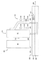
110 磁気ディスク
120 アクチュエータ
130 アクチュエータアーム
131 アクチュエータ軸
140 スピンドルモーター
150 シャーシ
200 読み取り/書き込みヘッド
202 磁気ディスク
204 磁気データ記録層
206 磁気透過性下層
209 媒体対向面
211 矢印
212 磁化領域
218 薄膜コイル
219 非磁性材料
220 磁気書き込みヘッド
222 磁気読み取りセンサ
224 磁気回路
230 検出素子
232 主磁極
300 読み取りヘッド
301 下層
302 センサ積層体
304 磁化固定層
306 スペーサ層
308 磁化自由層
310 非磁性層
312 磁性層
314 二重キャッピング層
316 底部磁性層
318 非磁性スペーサ層
320 頂部磁性層
321 絶縁層
322 側面シールド
330 第2の反強磁性層
350 センサ積層体
400 読み取りヘッドセンサ
401、402、403、406、407 磁性層
405 頂部磁性層
408 底部磁性層
602 コイル構造
604 コイル巻線
606 電源
S1 下部シールド
S2 上部シールド
Claims (19)
- 下部シールドと、
前記下部シールドの上に配置された上部シールドと、
前記下部シールドと前記上部シールドの間に配置されたセンサ積層体と、
前記下部シールドの上方且つ前記上部シールドの下方で前記センサ積層体に隣接して配置された側面シールドと、
を含む読み取りヘッドセンサであって、
前記センサ積層体が、
磁化固定層と、
前記磁化固定層の上方に配置されたスペーサ層と、
前記スペーサ層の上方に配置された磁化自由層と、
前記磁化自由層の上に配置された二重キャッピング層であって、非磁性層の上に配置された磁性層を含む二重キャッピング層を含み、
前記上部シールドが、
第1の磁性層及び前記第1の磁性層の上に配置された第2の磁性層を含む底部磁性層と、
前記底部磁性層の上に配置された第1の非磁性層と、
前記第1の非磁性層に配置され、且つ3層磁性積層膜を含む頂部磁性層と、
前記頂部磁性層の上に配置された反強磁性層と、を更に含む、読み取りヘッドセンサ。 - 前記二重キャッピング層内の前記磁性層がNiFe、CoFe、又はNiCoFeを含んでいる請求項1に記載の読み取りヘッドセンサ。
- 前記非磁性層がTaである、請求項1に記載の読み取りヘッドセンサ。
- 前記非磁性層の厚さが1nm未満である、請求項1に記載の読み取りヘッドセンサ。
- 前記底部磁性層内の前記第1の及び前記第2の磁性層が、NiFe、CoFe、又はNiCoFeのうち少なくとも1つから選択されている、請求項1に記載の読み取りヘッドセンサ。
- 前記第2の磁性層がCoFeであり、前記第1の磁性層がNiFeである、請求項5に記載の読み取りヘッドセンサ。
- 前記頂部磁性層内の前記3層磁性積層膜が、複数のCoFe層の間に挟まれたNiFe層を含む、請求項1に記載の読み取りヘッドセンサ。
- 前記側面シールドに結合されたコイル構造を更に含む、請求項7に記載の読み取りヘッドセンサ。
- 前記側面シールドに結合されたコイル構造を更に含む、請求項1に記載の読み取りヘッドセンサ。
- 下部シールドと、
前記下部シールドの上に配置された上部シールドと、
前記下部シールドと前記上部シールドの間に配置されたセンサ積層体と、
前記下部シールドの上方且つ前記上部シールドの下方に配置されたセンサ積層体に隣接して配置された側面シールドと、を含む読み取りヘッドセンサであって、
前記上部シールドが、
第1の磁性層及び前記第1の磁性層の上に配置された第2の磁性層を含む底部磁性層と、
前記底部磁性層の上に配置された第1の非磁性層と、
前記第1の非磁性層の上に配置され、且つ3層磁性積層膜を含む頂部磁性層と、
前記頂部磁性層の上に配置された反強磁性層と、を含む、読み取りヘッドセンサ。 - 前記底部磁性層内の前記第1の及び前記第2の磁性層が、NiFe、CoFe、又はNiCoFeのうち少なくとも1つから選択される、請求項10に記載の読み取りヘッドセンサ。
- 前記第2の磁性層がCoFeであり、前記第1の磁性層がNiFeである、請求項10に記載の読み取りヘッドセンサ。
- 前記頂部磁性層内の前記3層磁性積層膜が、複数のCoFe層の間に挟まれたNiFe層を含む、請求項10に記載の読み取りヘッドセンサ。
- 前記センサ積層体が
磁化固定層と、
前記磁化固定層の上方に配置されたスペーサ層と、
前記スペーサ層の上方に配置された磁化自由層と、
前記磁化自由層の上に配置された二重キャッピング層であって、非磁性層の上に配置された磁性層を含む二重キャッピング層を更に含む、請求項10に記載の読み取りヘッドセンサ。 - 前記二重キャッピング層内の磁性層が、NiFe、CoFe、又はNiCoFeを含む、請求項14に記載の読み取りヘッドセンサ。
- 前記非磁性層がTaである、請求項14に記載の読み取りヘッドセンサ。
- 前記非磁性層の厚さが1nm未満である、請求項14に記載の読み取りヘッドセンサ。
- 下部シールドと、
前記下部シールドの上に配置された上部シールドと、
前記下部シールドと前記上部シールドの間に配置されたセンサ積層体と、
前記下部シールドの上方且つ前記上部シールドの下方に配置された前記センサ積層体に隣接して配置された側面シールドと、
前記側面シールドに結合して配置されたコイル構造と、を含み、
前記上部シールドが、
第1の磁性層及び前記第1の磁性層の上に配置された第2の磁性層を含む底部磁性層と、
前記底部磁性層の上に配置された第1の非磁性層と、
前記第1の非磁性層に配置され、且つ3層磁性積層膜を含む頂部磁性層と、
前記頂部磁性層の上に配置された反強磁性層と、を更に含む、読み取りヘッドセンサ。 - 前記センサ積層体が
磁化固定層と、
前記磁化固定層の上方に配置されたスペーサ層と、
前記スペーサ層の上方に配置された磁化自由層と、
前記磁化自由層の上に配置され、且つTa層の上に配置されたNiFe層を含む二重キャッピング層と、を更に含む、請求項18に記載の読み取りヘッドセンサ。
Applications Claiming Priority (2)
| Application Number | Priority Date | Filing Date | Title |
|---|---|---|---|
| US14/166,699 | 2014-01-28 | ||
| US14/166,699 US9183858B2 (en) | 2014-01-28 | 2014-01-28 | Dual capping layer utilized in a magnetoresistive effect sensor |
Publications (2)
| Publication Number | Publication Date |
|---|---|
| JP2015141732A JP2015141732A (ja) | 2015-08-03 |
| JP5944022B2 true JP5944022B2 (ja) | 2016-07-05 |
Family
ID=52673916
Family Applications (1)
| Application Number | Title | Priority Date | Filing Date |
|---|---|---|---|
| JP2015014108A Active JP5944022B2 (ja) | 2014-01-28 | 2015-01-28 | 磁気抵抗効果センサに利用される二重キャッピング層 |
Country Status (9)
| Country | Link |
|---|---|
| US (1) | US9183858B2 (ja) |
| JP (1) | JP5944022B2 (ja) |
| KR (1) | KR20150089973A (ja) |
| CN (1) | CN104810026A (ja) |
| DE (1) | DE102015001085A1 (ja) |
| GB (2) | GB2523467A (ja) |
| IE (1) | IE20150021A1 (ja) |
| IN (1) | IN2015DE00237A (ja) |
| SG (1) | SG10201500652TA (ja) |
Families Citing this family (10)
| Publication number | Priority date | Publication date | Assignee | Title |
|---|---|---|---|---|
| US20150287426A1 (en) * | 2014-04-07 | 2015-10-08 | HGST Netherlands B.V. | Magnetic read head having spin hall effect layer |
| US9633679B2 (en) * | 2014-05-06 | 2017-04-25 | Seagate Technology Llc | Sensor stack structure with RKKY coupling layer between free layer and capping layer |
| JP6448282B2 (ja) * | 2014-10-01 | 2019-01-09 | 株式会社東芝 | 磁気ヘッド、磁気ヘッドアセンブリ、磁気記録再生装置、および磁気ヘッドの製造方法 |
| US10008224B2 (en) | 2016-03-11 | 2018-06-26 | Western Digital Technologies, Inc. | Magnetic read head with floating trailing shield |
| US9947347B1 (en) | 2016-12-20 | 2018-04-17 | Western Digital Technologies, Inc. | Magnetic sensor using inverse spin hall effect |
| WO2018182697A1 (en) * | 2017-03-31 | 2018-10-04 | Intel Corporation | Magnetic tunnel junction (mtj) devices with a sidewall passivation layer and methods to for the same |
| US10032365B1 (en) * | 2017-10-16 | 2018-07-24 | Universal Electronics Inc. | Apparatus, system and method for using a universal controlling device for displaying a graphical user element in a display device |
| JP6658982B2 (ja) * | 2017-10-16 | 2020-03-04 | Tdk株式会社 | トンネル磁気抵抗効果素子、磁気メモリ、及び内蔵型メモリ |
| US10872626B2 (en) | 2018-03-06 | 2020-12-22 | Western Digital Technologies, Inc. | MAMR stack shape optimization for magnetic recording |
| US10719298B1 (en) * | 2019-02-25 | 2020-07-21 | Western Digital Technologies, Inc. | System for generating random noise with a magnetic device |
Family Cites Families (28)
| Publication number | Priority date | Publication date | Assignee | Title |
|---|---|---|---|---|
| US6456467B1 (en) * | 2000-03-31 | 2002-09-24 | Seagate Technology Llc | Laminated shields with antiparallel magnetizations |
| US6700757B2 (en) | 2001-01-02 | 2004-03-02 | Hitachi Global Storage Technologies Netherlands B.V. | Enhanced free layer for a spin valve sensor |
| US7196881B2 (en) * | 2004-03-08 | 2007-03-27 | Hitachi Global Storage Technologies Netherlands B.V. | Adaptive domain stabilization for magnetic recording read sensors |
| US20060114620A1 (en) | 2004-11-30 | 2006-06-01 | Tdk Corporation | Granular type free layer and magnetic head |
| WO2007105459A1 (ja) * | 2006-03-10 | 2007-09-20 | Canon Anelva Corporation | 磁気抵抗効果型薄膜磁気ヘッド及びその製造方法 |
| US7672091B2 (en) * | 2006-03-15 | 2010-03-02 | Seagate Technology Llc | Reset device for biasing element in a magnetic sensor |
| US7672093B2 (en) * | 2006-10-17 | 2010-03-02 | Magic Technologies, Inc. | Hafnium doped cap and free layer for MRAM device |
| US7715155B2 (en) | 2007-04-11 | 2010-05-11 | Tdk Corporation | Thin-film magnetic head and manufacturing method thereof |
| US9442171B2 (en) * | 2008-01-09 | 2016-09-13 | Seagate Technology Llc | Magnetic sensing device with reduced shield-to-shield spacing |
| US8514524B2 (en) * | 2008-05-09 | 2013-08-20 | Headway Technologies, Inc. | Stabilized shields for magnetic recording heads |
| US8184411B2 (en) * | 2009-10-26 | 2012-05-22 | Headway Technologies, Inc. | MTJ incorporating CoFe/Ni multilayer film with perpendicular magnetic anisotropy for MRAM application |
| US8953285B2 (en) | 2010-05-05 | 2015-02-10 | Headway Technologies, Inc. | Side shielded magnetoresistive (MR) read head with perpendicular magnetic free layer |
| US8089734B2 (en) | 2010-05-17 | 2012-01-03 | Tdk Corporation | Magnetoresistive element having a pair of side shields |
| US8922956B2 (en) | 2010-06-04 | 2014-12-30 | Seagate Technology Llc | Tunneling magneto-resistive sensors with buffer layers |
| US8514525B2 (en) | 2010-09-13 | 2013-08-20 | HGST Netherlands B.V. | Current-perpendicular-to-the-plane (CPP) magnetoresistive (MR) sensor with reference layer integrated in magnetic shield |
| US20120063034A1 (en) | 2010-09-13 | 2012-03-15 | Hitachi Global Storage Technologies Netherlands B.V. | Current-perpendicular-to-the-plane (cpp) magnetoresistive (mr) sensor with improved insulating structure |
| US8437106B2 (en) * | 2010-10-08 | 2013-05-07 | Tdk Corporation | Thin film magnetic head including spin-valve film with free layer magnetically connected with shield |
| US8553370B2 (en) | 2010-11-24 | 2013-10-08 | HGST Netherlands B.V. | TMR reader structure having shield layer |
| US8553371B2 (en) | 2010-11-24 | 2013-10-08 | HGST Netherlands B.V. | TMR reader without DLC capping structure |
| US20120327537A1 (en) * | 2011-06-23 | 2012-12-27 | Seagate Technology Llc | Shield Stabilization Configuration With Applied Bias |
| US8462461B2 (en) * | 2011-07-05 | 2013-06-11 | HGST Netherlands B.V. | Spin-torque oscillator (STO) with magnetically damped free layer |
| US8611053B2 (en) | 2012-03-08 | 2013-12-17 | HGST Netherlands B.V. | Current-perpendicular-to-the-plane (CPP) magnetoresistive sensor with multilayer reference layer including a Heusler alloy |
| US8797692B1 (en) * | 2012-09-07 | 2014-08-05 | Western Digital (Fremont), Llc | Magnetic recording sensor with AFM exchange coupled shield stabilization |
| US8531801B1 (en) * | 2012-12-20 | 2013-09-10 | Western Digital (Fremont), Llc | Method and system for providing a read transducer having a composite magnetic shield with smooth interfaces |
| US9123886B2 (en) * | 2013-03-05 | 2015-09-01 | Headway Technologies, Inc. | High moment wrap-around shields for magnetic read head improvements |
| US8780505B1 (en) * | 2013-03-12 | 2014-07-15 | Western Digital (Fremont), Llc | Method and system for providing a read transducer having an improved composite magnetic shield |
| US8780506B1 (en) * | 2013-06-20 | 2014-07-15 | HGST Netherlands B.V. | Current-perpendicular-to-the-plane (CPP) magnetoresistive (MR) sensor with side shields and an antiparallel structure top shield |
| US9087525B2 (en) * | 2013-10-30 | 2015-07-21 | Seagate Technology Llc | Layered synthetic anti-ferromagnetic upper shield |
-
2014
- 2014-01-28 US US14/166,699 patent/US9183858B2/en active Active
-
2015
- 2015-01-26 GB GB1501239.6A patent/GB2523467A/en not_active Withdrawn
- 2015-01-26 GB GB1516399.1A patent/GB2531906A/en not_active Withdrawn
- 2015-01-27 IE IE20150021A patent/IE20150021A1/en not_active IP Right Cessation
- 2015-01-27 SG SG10201500652TA patent/SG10201500652TA/en unknown
- 2015-01-28 IN IN237DE2015 patent/IN2015DE00237A/en unknown
- 2015-01-28 KR KR1020150013618A patent/KR20150089973A/ko active IP Right Grant
- 2015-01-28 DE DE102015001085.9A patent/DE102015001085A1/de not_active Withdrawn
- 2015-01-28 CN CN201510100220.6A patent/CN104810026A/zh active Pending
- 2015-01-28 JP JP2015014108A patent/JP5944022B2/ja active Active
Also Published As
| Publication number | Publication date |
|---|---|
| DE102015001085A1 (de) | 2015-07-30 |
| IN2015DE00237A (ja) | 2015-07-31 |
| IE20150021A1 (en) | 2015-07-29 |
| SG10201500652TA (en) | 2015-08-28 |
| GB201501239D0 (en) | 2015-03-11 |
| US9183858B2 (en) | 2015-11-10 |
| CN104810026A (zh) | 2015-07-29 |
| KR20150089973A (ko) | 2015-08-05 |
| GB2523467A (en) | 2015-08-26 |
| GB2531906A (en) | 2016-05-04 |
| JP2015141732A (ja) | 2015-08-03 |
| US20150213816A1 (en) | 2015-07-30 |
| GB201516399D0 (en) | 2015-10-28 |
Similar Documents
| Publication | Publication Date | Title |
|---|---|---|
| JP5944022B2 (ja) | 磁気抵抗効果センサに利用される二重キャッピング層 | |
| US9190081B2 (en) | AF-coupled dual side shield reader with AF-coupled USL | |
| US8077435B1 (en) | Current perpendicular-to-plane read sensor with back shield | |
| KR101789589B1 (ko) | 센서 스택 구조 | |
| JP5798089B2 (ja) | センサ積層体、シールド、および第1のシールド安定化構造を備える装置、センサ積層体、シールド、および磁性層を備える装置、データ記憶媒体、記録ヘッド、およびアームを備える装置 | |
| JP5781468B2 (ja) | 磁気抵抗シールド | |
| US8638530B1 (en) | Current-perpendicular-to-the-plane (CPP) magnetoresistive (MR) sensor having a top shield with an antiparallel structure | |
| KR101566291B1 (ko) | 결합된 측면 실드를 갖는 자기 엘리먼트 | |
| US20150287426A1 (en) | Magnetic read head having spin hall effect layer | |
| JP2010140524A (ja) | 差動型磁気抵抗効果ヘッド及び磁気記録再生装置 | |
| US9230578B2 (en) | Multiple readers for high resolution and SNR for high areal density application | |
| US8958180B1 (en) | Capping materials for magnetic read head sensor | |
| JP2007531179A (ja) | 安定化スピンバルブヘッドとその製造方法 | |
| JP2007531178A (ja) | 磁気抵抗ヘッド用安定化器及び製造方法 | |
| US9406322B2 (en) | Graded side shield gap reader | |
| US9177588B2 (en) | Recessed IRMN reader process | |
| US9087525B2 (en) | Layered synthetic anti-ferromagnetic upper shield | |
| US9251815B2 (en) | Magnetoresistive sensor with AFM-stabilized bottom shield | |
| US9454979B1 (en) | Sensor structure with multilayer top shield | |
| US8902549B1 (en) | Enhanced pinning property by inserted Si seed layer | |
| JP5872664B2 (ja) | 非対称感度リーダ | |
| US20240144966A1 (en) | Middle Shields Two-Dimensional Magnetic Recording Read Heads |
Legal Events
| Date | Code | Title | Description |
|---|---|---|---|
| A977 | Report on retrieval |
Free format text: JAPANESE INTERMEDIATE CODE: A971007 Effective date: 20151120 |
|
| A131 | Notification of reasons for refusal |
Free format text: JAPANESE INTERMEDIATE CODE: A131 Effective date: 20160105 |
|
| A521 | Request for written amendment filed |
Free format text: JAPANESE INTERMEDIATE CODE: A523 Effective date: 20160405 |
|
| TRDD | Decision of grant or rejection written | ||
| A01 | Written decision to grant a patent or to grant a registration (utility model) |
Free format text: JAPANESE INTERMEDIATE CODE: A01 Effective date: 20160426 |
|
| A61 | First payment of annual fees (during grant procedure) |
Free format text: JAPANESE INTERMEDIATE CODE: A61 Effective date: 20160524 |
|
| R150 | Certificate of patent or registration of utility model |
Ref document number: 5944022 Country of ref document: JP Free format text: JAPANESE INTERMEDIATE CODE: R150 |
|
| R250 | Receipt of annual fees |
Free format text: JAPANESE INTERMEDIATE CODE: R250 |
|
| S111 | Request for change of ownership or part of ownership |
Free format text: JAPANESE INTERMEDIATE CODE: R313113 |
|
| R350 | Written notification of registration of transfer |
Free format text: JAPANESE INTERMEDIATE CODE: R350 |
|
| R250 | Receipt of annual fees |
Free format text: JAPANESE INTERMEDIATE CODE: R250 |
|
| R250 | Receipt of annual fees |
Free format text: JAPANESE INTERMEDIATE CODE: R250 |
|
| R250 | Receipt of annual fees |
Free format text: JAPANESE INTERMEDIATE CODE: R250 |
|
| R250 | Receipt of annual fees |
Free format text: JAPANESE INTERMEDIATE CODE: R250 |