JP5941783B2 - Imaging device - Google Patents
Imaging device Download PDFInfo
- Publication number
- JP5941783B2 JP5941783B2 JP2012173175A JP2012173175A JP5941783B2 JP 5941783 B2 JP5941783 B2 JP 5941783B2 JP 2012173175 A JP2012173175 A JP 2012173175A JP 2012173175 A JP2012173175 A JP 2012173175A JP 5941783 B2 JP5941783 B2 JP 5941783B2
- Authority
- JP
- Japan
- Prior art keywords
- unit
- input terminal
- comparison
- voltage
- column
- Prior art date
- Legal status (The legal status is an assumption and is not a legal conclusion. Google has not performed a legal analysis and makes no representation as to the accuracy of the status listed.)
- Expired - Fee Related
Links
Images


Classifications
-
- H—ELECTRICITY
- H04—ELECTRIC COMMUNICATION TECHNIQUE
- H04N—PICTORIAL COMMUNICATION, e.g. TELEVISION
- H04N25/00—Circuitry of solid-state image sensors [SSIS]; Control thereof
- H04N25/70—SSIS architectures; Circuits associated therewith
- H04N25/76—Addressed sensors, e.g. MOS or CMOS sensors
-
- H—ELECTRICITY
- H04—ELECTRIC COMMUNICATION TECHNIQUE
- H04N—PICTORIAL COMMUNICATION, e.g. TELEVISION
- H04N25/00—Circuitry of solid-state image sensors [SSIS]; Control thereof
- H04N25/70—SSIS architectures; Circuits associated therewith
- H04N25/71—Charge-coupled device [CCD] sensors; Charge-transfer registers specially adapted for CCD sensors
- H04N25/75—Circuitry for providing, modifying or processing image signals from the pixel array
Description
本発明は、撮像装置に関する。 The present invention relates to an imaging apparatus.
従来例に係るAD変換方法を用いた撮像装置として、特許文献1に記載された構成が知られている。初めに、特許文献1に記載された撮像装置の構成および動作について説明する。
As an imaging apparatus using an AD conversion method according to a conventional example, a configuration described in
図16は、特許文献1に記載された従来例に係るAD変換方法を用いた(C)MOS撮像装置の概略構成を示している。撮像装置1001は、撮像部1002、垂直選択部1012、読出し電流源部1005、アナログ部1006、カラム処理部1015、参照信号生成部1016、水平選択部1014、出力部1017、変更部1018、タイミング制御部1020で構成されている。
FIG. 16 shows a schematic configuration of a (C) MOS imaging device using the AD conversion method according to the conventional example described in
タイミング制御部1020は、垂直選択部1012、読出し電流源部1005、アナログ部1006、カラム処理部1015、参照信号生成部1016、水平選択部1014、および出力部1017などの各部を制御する。撮像部1002は、光電変換素子を有する単位画素1003が行列状に配置されて構成され、入射される電磁波の大きさに応じた画素信号を生成し、列毎に設けられた垂直信号線1013へ出力する。
The
垂直選択部1012は、撮像部1002の各単位画素1003の駆動に際して、行制御線1011を介して撮像部1002の行アドレスや行走査の制御を行う。水平選択部1014は、カラム処理部1015の列AD変換部1030の列アドレスや列走査の制御を行う。読出し電流源部1005は、撮像部1002からの画素信号を電圧信号として読み出すための電流源である。アナログ部1006は、必要に応じて増幅等を実施する。
The
カラム処理部1015は、変更部1018と、撮像部1002の列毎に設けられた列AD変換部1030とを有する。変更部1018は、列AD変換部1030に与えられる電圧を変更する。列AD変換部1030は、撮像部1002の各単位画素1003から列毎に出力される画素信号であるアナログ信号をデジタルデータに変換して出力する。参照信号生成部1016は、例えば積分回路やDAC回路で構成され、時間が経過するにつれてレベルが傾斜状に変化する参照信号Rampを生成する。
The
次に、列AD変換部1030の構成について説明する。図17は、列AD変換部1030を含むカラム処理部1015の構成を示している。列AD変換部1030は全て同一に構成され、各々の列AD変換部1030は、比較部1031、計測部1032を有する構成となっている。
Next, the configuration of the column
比較部1031は、一般的に良く知られている差動アンプを基本構成とするコンパレータ回路である。比較部1031は、撮像部1002の単位画素1003から出力される画素信号と参照信号Rampとを比較し、例えば参照信号Rampが画素信号よりも大なるときはHighレベル、例えば参照信号Rampが画素信号よりも小なるときはLowレベルを出力する。
The
計測部1032は、アップ/ダウンカウンタ回路で構成され、比較部1031が比較を開始してから比較を終了するまでの比較時間を計測する。これにより、画素信号の大きさに応じた比較時間の計測値が得られる。水平選択部1014は、シフトレジスタやデコーダなどによって構成され、カラム処理部1015における各列AD変換部1030の列アドレスや列走査の制御を行う。これにより、AD変換されたデジタルデータは順に水平信号線を経由して出力部1017に出力される。
The
変更部1018はスイッチ素子で構成されている。スイッチ素子の一端は、全ての列の比較部1031の2つの入力端子のうち、参照信号Rampが与えられる入力端子に接続され、スイッチ素子の他端は電源VDDに接続されている。変更部1018を構成するスイッチ素子がON(活性化)されることで、参照信号Rampが与えられる比較部1031の入力端子は電源VDDに短絡される。
The
比較部1031による比較動作は、比較部1031を構成する差動アンプの2つの入力端子の電圧のリセット(バランス)が行われた後に開始される。リセット動作後に、比較部1031を構成する差動アンプの2つの入力端子の電圧に多少のばらつきが残ることにより、比較部1031の出力が反転しなかったり、参照信号Rampの入力後直ちに比較部1031の出力が反転したりする不具合を防ぐため、撮像装置1001に変更部1018が設けられている。
The comparison operation by the
次に、AD変換動作について説明する。単位画素1003の具体的な動作については説明を省略するが、単位画素1003からは画素信号としてリセットレベルと信号レベルとが出力される。
Next, the AD conversion operation will be described. Although the description of the specific operation of the
まず、単位画素1003からのリセットレベルの読出しが安定した後、比較部1031を構成する差動アンプの2つの入力端子の電圧のリセットが行われる。続いて、変更部1018により、参照信号Rampが与えられた入力端子に所定の電圧(オフセット)が印加される。その後、比較部1031は、その所定の電圧を比較開始の電圧として参照信号Rampとリセットレベルとの比較を行い、参照信号Rampがリセットレベルに対して所定の条件を満たしたタイミングで比較処理を終了する。計測部1032はダウンカウントモードで計測を実施し、比較処理の終了時点の計測値がリセットレベルのデジタルデータとなる。
First, after the reset level reading from the
続いて、単位画素1003からの信号レベルの読出し時には、比較部1031におけるリセット動作および変更部1018による変更動作は行わない。単位画素1003からの信号レベルの読出しが安定した後、比較部1031は、上記所定の電圧を比較開始の電圧として参照信号Rampと信号レベルとの比較を行い、参照信号Rampが信号レベルに対して所定の条件を満たしたタイミングで比較処理を終了する。計測部1032はアップカウントモードで計測を実施し、比較終了時点の計測部1032の計測値が信号成分(信号レベルからリセットレベルを減算した信号)のデジタルデータとなる。
Subsequently, when the signal level is read from the
以上のように、画素信号をAD変換することが可能となる。また、リセット動作後に、比較部1031を構成する差動アンプの2つの入力端子の電圧に多少のばらつきが残ったとしても、変更部1018により、参照信号Rampが与えられる入力端子にオフセットを印加することで、参照信号Rampが与えられる入力端子の電圧が、画素信号が与えられる入力端子の電圧よりも高くなるため、比較部1031の出力を比較動作中に確実に反転させることができる。
As described above, the pixel signal can be AD converted. In addition, after the reset operation, even if some variation remains in the voltages of the two input terminals of the differential amplifier constituting the
しかしながら、上記の従来の撮像装置には以下に示す問題がある。 However, the above conventional imaging apparatus has the following problems.
(1)差動アンプの入力端子の電圧を直接変更する構成に関する問題
リセット後の差動アンプの2つの入力端子の電圧はリセット電圧VRSTに略一致する。リセットが行われた後、変更部1018を構成するスイッチ素子が制御(ON)されることで、参照信号が与えられる入力端子にオフセットが印加された後、AD変換が行われる。このように、参照信号が与えられる入力端子にオフセットを印加することで、比較部1031の出力を比較動作中に確実に反転させることができ、AD変換精度が向上する。しかし、一行の画素数分の差動アンプの入力端子に一様なオフセットが印加されるだけであるので、一行の画素数分の比較部1031が同時に比較処理を終了する可能性が高い。特に、リセットレベルのAD変換時に、一行の画素数分の比較部1031が同時に比較処理を終了することが考えられる。比較部1031では、比較処理の終了時に、比較部1031を構成する差動アンプ内のトランジスタのオン/オフの切替による電流が流れる。このため、一行の画素数分の比較部1031が同時に比較処理を終了すると、電力集中による電圧降下に起因する誤動作の問題がある。
(1) Problems related to the configuration in which the voltage at the input terminal of the differential amplifier is directly changed The voltages at the two input terminals of the differential amplifier after reset are approximately equal to the reset voltage V RST . After the reset is performed, the switch element configuring the changing
(2)差動アンプの入力端子の電圧を参照信号の制御で間接的に変更する構成に関して
上記の方法に代えて、参照信号を制御することで、参照信号が与えられる入力端子の電圧を所定の電圧に変更することが考えられる。この場合も同様に、AD変換精度が向上する。しかし、一行の画素数分の差動アンプの入力端子に一様なオフセットが印加されることに変わりはなく、一行の画素数分の比較部1031が同時に比較処理を終了する可能性が高い。したがって、電力集中による電圧降下に起因する誤動作の問題がある。
(2) Regarding a configuration in which the voltage at the input terminal of the differential amplifier is indirectly changed by controlling the reference signal In place of the above method, the voltage at the input terminal to which the reference signal is given is predetermined by controlling the reference signal. It is conceivable to change the voltage to In this case as well, the AD conversion accuracy is improved. However, a uniform offset is still applied to the input terminals of the differential amplifier for the number of pixels in one row, and there is a high possibility that the
本発明は、上述した課題に鑑みてなされたものであって、より高精度なAD変換を行うことができる撮像装置を提供することを目的とする。 The present invention has been made in view of the above-described problems, and an object thereof is to provide an imaging apparatus capable of performing AD conversion with higher accuracy.
本発明は、上記の課題を解決するためになされたもので、光電変換素子を有する複数の単位画素が行列状に配置され、前記単位画素の配列の列毎に対応する列信号線にアナログ信号を出力する撮像部と、時間の経過とともに増加あるいは減少する参照信号を生成する参照信号生成部と、前記撮像部の各単位画素を前記単位画素の配列の行毎に選択制御する行選択部と、前記列信号線と電気的に接続された第1の入力端子と、第1の容量素子を介して前記参照信号生成部と電気的に接続された第2の入力端子とを有し、前記第1の入力端子および前記第2の入力端子の電圧を比較する差動アンプ部と、前記第1の入力端子および前記第2の入力端子の電圧をリセットするリセット部と、を有する比較部と、前記比較部による比較開始から比較終了までの比較時間を計測する計測部と、スイッチ素子を有し、前記スイッチ素子の一端は前記第2の入力端子に接続され、前記スイッチ素子の他端は、前記リセット部によるリセット動作後に電圧源に接続され、前記第1の入力端子と前記第2の入力端子の電圧差が、前記比較部による比較動作を保証する電圧となるように前記電圧源の電圧に応じたオフセットを前記第2の入力端子に印加する変更部と、を有し、前記撮像部に配置された複数の前記単位画素は、第1の画素群に含まれる前記単位画素と、前記第1の画素群と異なる第2の画素群に含まれる前記単位画素とを有し、前記第1の画素群に含まれる前記単位画素の配列のいずれかの列に対応する前記列信号線に接続された前記比較部の前記第2の入力端子に印加される前記オフセットと、前記第2の画素群に含まれる前記単位画素の配列のいずれかの列に対応する前記列信号線に接続された前記比較部の前記第2の入力端子に印加される前記オフセットとが異なることを特徴とする撮像装置である。
また、本発明の撮像装置において、前記第1の画素群に含まれる前記単位画素の配列のいずれかの列に対応する前記列信号線に接続された前記比較部に係る前記変更部が有する前記スイッチ素子の他端が接続される前記電圧源の電圧値が、前記第2の画素群に含まれる前記単位画素の配列のいずれかの列に対応する前記列信号線に接続された前記比較部に係る前記変更部が有する前記スイッチ素子の他端が接続される前記電圧源の電圧値と異なることを特徴とする。
また、本発明は、光電変換素子を有する複数の単位画素が行列状に配置され、前記単位画素の配列の列毎に対応する列信号線にアナログ信号を出力する撮像部と、時間の経過とともに増加あるいは減少する参照信号を生成する参照信号生成部と、前記撮像部の各単位画素を前記単位画素の配列の行毎に選択制御する行選択部と、第1の容量素子を介して前記列信号線と電気的に接続された第1の入力端子と、前記参照信号生成部と電気的に接続された第2の入力端子とを有し、前記第1の入力端子および前記第2の入力端子の電圧を比較する差動アンプ部と、前記第1の入力端子および前記第2の入力端子の電圧をリセットするリセット部と、を有する比較部と、前記比較部による比較開始から比較終了までの比較時間を計測する計測部と、スイッチ素子と第2の容量素子を有し、前記第2の容量素子の一端は前記第1の入力端子に接続され、前記第2の容量素子の他端は、前記リセット部によるリセット動作時には前記スイッチ素子を介して第1の電圧源に接続され、前記リセット部によるリセット動作後には前記スイッチ素子を介して前記第1の電圧源と異なる第2の電圧源に接続され、前記第1の入力端子と前記第2の入力端子の電圧差が、前記比較部による比較動作を保証する電圧となるように前記第1の電圧源および前記第2の電圧源の電圧に応じたオフセットを前記第1の入力端子に印加する変更部と、を有し、前記撮像部に配置された複数の前記単位画素は、第1の画素群に含まれる前記単位画素と、前記第1の画素群と異なる第2の画素群に含まれる前記単位画素とを有し、前記第1の画素群に含まれる前記単位画素の配列のいずれかの列に対応する前記列信号線に接続された前記比較部の前記第1の入力端子に印加される前記オフセットと、前記第2の画素群に含まれる前記単位画素の配列のいずれかの列に対応する前記列信号線に接続された前記比較部の前記第1の入力端子に印加される前記オフセットとが異なることを特徴とする撮像装置である。
The present invention has been made to solve the above-described problem. A plurality of unit pixels having photoelectric conversion elements are arranged in a matrix, and an analog signal is applied to a column signal line corresponding to each column of the unit pixel array. An imaging unit that outputs a reference signal generation unit that generates a reference signal that increases or decreases over time, and a row selection unit that selectively controls each unit pixel of the imaging unit for each row of the unit pixel array, A first input terminal electrically connected to the column signal line, and a second input terminal electrically connected to the reference signal generation unit via a first capacitive element, A comparator having a differential amplifier that compares voltages of the first input terminal and the second input terminal, and a reset unit that resets voltages of the first input terminal and the second input terminal; The ratio from the start of comparison to the end of comparison by the comparison unit A measuring unit for measuring a comparison time; and a switch element, wherein one end of the switch element is connected to the second input terminal, and the other end of the switch element is connected to a voltage source after a reset operation by the reset unit And the second input terminal is offset according to the voltage of the voltage source so that the voltage difference between the first input terminal and the second input terminal is a voltage that guarantees a comparison operation by the comparison unit. A plurality of unit pixels arranged in the imaging unit, the unit pixels included in the first pixel group, and a second pixel different from the first pixel group And the second unit of the comparison unit connected to the column signal line corresponding to any column of the array of unit pixels included in the first pixel group. The offset applied to the input terminal and the second pixel group An image pickup apparatus, wherein the offset applied to the second input terminal of the comparison unit connected to the column signal line corresponding to any column of the unit pixel array included in the unit pixel is different It is.
In the imaging device according to the aspect of the invention, the change unit according to the comparison unit connected to the column signal line corresponding to any column of the unit pixel array included in the first pixel group may include the change unit. The comparison unit in which the voltage value of the voltage source to which the other end of the switch element is connected is connected to the column signal line corresponding to any column of the unit pixel array included in the second pixel group It is different from the voltage value of the said voltage source to which the other end of the said switch element which the said change part which concerns on has is connected.
In addition, the present invention provides an imaging unit in which a plurality of unit pixels having photoelectric conversion elements are arranged in a matrix, and outputs an analog signal to a column signal line corresponding to each column of the unit pixel array, and over time A reference signal generation unit that generates a reference signal that increases or decreases, a row selection unit that selects and controls each unit pixel of the imaging unit for each row of the unit pixel array, and the column via a first capacitive element A first input terminal electrically connected to a signal line; and a second input terminal electrically connected to the reference signal generation unit; the first input terminal and the second input A comparison unit having a differential amplifier unit for comparing terminal voltages, a reset unit for resetting voltages of the first input terminal and the second input terminal, and from a comparison start to a comparison end by the comparison unit A measurement unit that measures the comparison time of A second capacitor element, and one end of the second capacitor element is connected to the first input terminal, and the other end of the second capacitor element is connected to the switch during a reset operation by the reset unit. Connected to a first voltage source via an element, and after a reset operation by the reset unit, connected to a second voltage source different from the first voltage source via the switch element, and the first input terminal And an offset according to the voltages of the first voltage source and the second voltage source so that a voltage difference between the second input terminal and the second input terminal is a voltage that guarantees a comparison operation by the comparison unit. A plurality of unit pixels arranged in the imaging unit, and a second pixel different from the first pixel group. And the unit pixel included in the pixel group, and included in the first pixel group The offset applied to the first input terminal of the comparison unit connected to the column signal line corresponding to any column of the unit pixel array, and the second pixel group The imaging apparatus is characterized in that the offset applied to the first input terminal of the comparison unit connected to the column signal line corresponding to any column of the unit pixel array is different.
また、本発明は、光電変換素子を有する複数の単位画素が行列状に配置され、前記単位画素の配列の列毎に対応する列信号線にアナログ信号を出力する撮像部と、時間の経過とともに増加あるいは減少する参照信号を生成する参照信号生成部と、前記撮像部の各単位画素を前記単位画素の配列の行毎に選択制御する行選択部と、前記列信号線と電気的に接続された第1の入力端子と、第1の容量素子を介して前記参照信号生成部と電気的に接続された第2の入力端子とを有し、前記第1の入力端子および前記第2の入力端子の電圧を比較する差動アンプ部と、前記第1の入力端子および前記第2の入力端子の電圧をリセットするリセット部と、を有する比較部と、前記比較部による比較開始から比較終了までの比較時間を計測する計測部と、スイッチ素子と第2の容量素子を有し、前記第2の容量素子の一端は前記第2の入力端子に接続され、前記第2の容量素子の他端は、前記リセット部によるリセット動作時には前記スイッチ素子を介して第1の電圧源に接続され、前記リセット部によるリセット動作後には前記スイッチ素子を介して前記第1の電圧源と異なる第2の電圧源に接続され、前記第1の入力端子と前記第2の入力端子の電圧差が、前記比較部による比較動作を保証する電圧となるように前記第1の電圧源および前記第2の電圧源の電圧に応じたオフセットを前記第2の入力端子に印加する変更部と、を有し、前記撮像部に配置された複数の前記単位画素は、第1の画素群に含まれる前記単位画素と、前記第1の画素群と異なる第2の画素群に含まれる前記単位画素とを有し、前記第1の画素群に含まれる前記単位画素の配列のいずれかの列に対応する前記列信号線に接続された前記比較部の前記第2の入力端子に印加される前記オフセットと、前記第2の画素群に含まれる前記単位画素の配列のいずれかの列に対応する前記列信号線に接続された前記比較部の前記第2の入力端子に印加される前記オフセットとが異なることを特徴とする撮像装置である。 In addition, the present invention provides an imaging unit in which a plurality of unit pixels having photoelectric conversion elements are arranged in a matrix, and outputs an analog signal to a column signal line corresponding to each column of the unit pixel array, and over time A reference signal generation unit that generates a reference signal that increases or decreases, a row selection unit that selects and controls each unit pixel of the imaging unit for each row of the unit pixel array, and the column signal line are electrically connected. A first input terminal and a second input terminal electrically connected to the reference signal generation unit via a first capacitive element, the first input terminal and the second input A comparison unit having a differential amplifier unit for comparing terminal voltages, a reset unit for resetting voltages of the first input terminal and the second input terminal, and from a comparison start to a comparison end by the comparison unit A measurement unit that measures the comparison time of A second capacitor element, and one end of the second capacitor element is connected to the second input terminal, and the other end of the second capacitor element is the switch during a reset operation by the reset unit. Connected to a first voltage source via an element, and after a reset operation by the reset unit, connected to a second voltage source different from the first voltage source via the switch element, and the first input terminal And an offset according to the voltages of the first voltage source and the second voltage source so that a voltage difference between the second input terminal and the second input terminal is a voltage that guarantees a comparison operation by the comparison unit. A plurality of unit pixels arranged in the imaging unit, and a second pixel different from the first pixel group. And the unit pixel included in the pixel group, and included in the first pixel group The offset applied to the second input terminal of the comparison unit connected to the column signal line corresponding to any column of the unit pixel array, and the second pixel group includes the offset The imaging apparatus is characterized in that the offset applied to the second input terminal of the comparison unit connected to the column signal line corresponding to any column of the unit pixel array is different.
また、本発明の撮像装置において、前記第1の画素群に含まれる前記単位画素の配列のいずれかの列に対応する前記列信号線に接続された前記比較部に係る前記変更部が有する前記第2の容量素子の容量値と、前記第2の画素群に含まれる前記単位画素の配列のいずれかの列に対応する前記列信号線に接続された前記比較部に係る前記変更部が有する前記第2の容量素子の容量値とが異なることを特徴とする。 In the imaging device according to the aspect of the invention, the change unit according to the comparison unit connected to the column signal line corresponding to any column of the unit pixel array included in the first pixel group may include the change unit. The change unit according to the comparison unit connected to the column signal line corresponding to any column of the capacitance value of the second capacitor element and the column of the unit pixels included in the second pixel group has The capacitance value of the second capacitor element is different.
また、本発明の撮像装置において、前記第1の画素群に含まれる前記単位画素の配列のいずれかの列に対応する前記列信号線に接続された前記比較部に係る前記変更部が有する前記第2の容量素子の他端が接続される前記第1の電圧源および前記第2の電圧源の少なくとも一方の電圧源の電圧値が、前記第2の画素群に含まれる前記単位画素の配列のいずれかの列に対応する前記列信号線に接続された前記比較部に係る前記変更部が有する前記第2の容量素子の他端が接続される前記第1の電圧源および前記第2の電圧源の少なくとも一方の電圧源の電圧値と異なることを特徴とする。 In the imaging device according to the aspect of the invention, the change unit according to the comparison unit connected to the column signal line corresponding to any column of the unit pixel array included in the first pixel group may include the change unit. The unit pixel array in which the voltage value of at least one of the first voltage source and the second voltage source to which the other end of the second capacitive element is connected is included in the second pixel group The first voltage source to which the other end of the second capacitive element of the change unit of the comparison unit connected to the column signal line corresponding to any one of the columns is connected and the second voltage source The voltage value is different from the voltage value of at least one of the voltage sources.
また、本発明の撮像装置において、前記第2の電圧源は前記アナログ信号であることを特徴とする。 In the imaging device of the present invention, the second voltage source is the analog signal.
また、本発明の撮像装置において、前記第2の電圧源は前記参照信号であることを特徴とする。 In the imaging device of the present invention, the second voltage source is the reference signal.
また、本発明は、光電変換素子を有する複数の単位画素が行列状に配置され、前記単位画素の配列の列毎に対応する列信号線にアナログ信号を出力する撮像部と、時間の経過とともに増加あるいは減少する参照信号を生成する参照信号生成部と、前記撮像部の各単位画素を前記単位画素の配列の行毎に選択制御する行選択部と、第1の容量素子を介して前記列信号線と電気的に接続された第1の入力端子と、前記参照信号生成部と電気的に接続された第2の入力端子とを有し、前記第1の入力端子および前記第2の入力端子の電圧を比較する差動アンプ部と、前記第1の入力端子および前記第2の入力端子の電圧をリセットするリセット部と、を有する比較部と、前記比較部による比較開始から比較終了までの比較時間を計測する計測部と、スイッチ素子を有し、前記スイッチ素子の一端は前記第1の入力端子に接続され、前記スイッチ素子の他端は、前記リセット部によるリセット動作後に電圧源に接続され、前記第1の入力端子と前記第2の入力端子の電圧差が、前記比較部による比較動作を保証する電圧となるように前記電圧源の電圧に応じたオフセットを前記第1の入力端子に印加する変更部と、を有し、前記撮像部に配置された複数の前記単位画素は、第1の画素群に含まれる前記単位画素と、前記第1の画素群と異なる第2の画素群に含まれる前記単位画素とを有し、前記第1の画素群に含まれる前記単位画素の配列のいずれかの列に対応する前記列信号線に接続された前記比較部の前記第1の入力端子に印加される前記オフセットと、前記第2の画素群に含まれる前記単位画素の配列のいずれかの列に対応する前記列信号線に接続された前記比較部の前記第1の入力端子に印加される前記オフセットとが異なることを特徴とする撮像装置である。 In addition, the present invention provides an imaging unit in which a plurality of unit pixels having photoelectric conversion elements are arranged in a matrix, and outputs an analog signal to a column signal line corresponding to each column of the unit pixel array, and over time A reference signal generation unit that generates a reference signal that increases or decreases, a row selection unit that selects and controls each unit pixel of the imaging unit for each row of the unit pixel array, and the column via a first capacitive element A first input terminal electrically connected to a signal line; and a second input terminal electrically connected to the reference signal generation unit; the first input terminal and the second input A comparison unit having a differential amplifier unit for comparing terminal voltages, a reset unit for resetting voltages of the first input terminal and the second input terminal, and from a comparison start to a comparison end by the comparison unit A measurement unit that measures the comparison time of One end of the switch element is connected to the first input terminal, and the other end of the switch element is connected to a voltage source after a reset operation by the reset unit, and the first input terminal and the A changing unit that applies an offset according to the voltage of the voltage source to the first input terminal so that the voltage difference of the second input terminal is a voltage that guarantees a comparison operation by the comparing unit. The plurality of unit pixels arranged in the imaging unit include the unit pixels included in a first pixel group and the unit pixels included in a second pixel group different from the first pixel group. The offset applied to the first input terminal of the comparison unit connected to the column signal line corresponding to any column of the unit pixel array included in the first pixel group, Any of the arrangement of the unit pixels included in the second pixel group The imaging apparatus is characterized in that the offset applied to the first input terminal of the comparison unit connected to the column signal line corresponding to the column is different.
本発明によれば、第1の画素群に含まれる単位画素の配列のいずれかの列に対応する列信号線に接続されたAD変換部の変更部が比較部の第1の入力端子または第2の入力端子に印加するオフセットと、第2の画素群に含まれる単位画素の配列のいずれかの列に対応する列信号線に接続されたAD変換部の変更部が比較部の第1の入力端子または第2の入力端子に印加するオフセットとが異なることによって、各比較部が略同時に比較を開始した場合でも、異なるタイミングで各比較部に比較を終了させることが可能となる。これによって、電力集中が低減されるので、より高精度なAD変換を行うことができる。 According to the present invention, the change unit of the AD conversion unit connected to the column signal line corresponding to any column of the unit pixel array included in the first pixel group is the first input terminal of the comparison unit or the first The change unit of the AD conversion unit connected to the column signal line corresponding to any column of the offset and the unit pixel array included in the second pixel group is the first applied to the comparison unit. Since the offset applied to the input terminal or the second input terminal is different, even when the comparison units start comparison at substantially the same time, the comparison units can finish the comparison at different timings. As a result, power concentration is reduced, so that AD conversion with higher accuracy can be performed.
以下、図面を参照し、本発明の実施形態を説明する。 Hereinafter, embodiments of the present invention will be described with reference to the drawings.
(第1の実施形態)
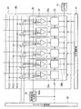
まず、本発明の第1の実施形態を説明する。図1は、本実施形態に係る(C)MOS撮像装置の構成の一例を示している。図1に示す撮像装置1は、撮像部2、垂直選択部12、カラム処理部15、参照信号生成部16、変更部18a、水平選択部14、出力部17、タイミング制御部20で構成されている。
(First embodiment)
First, a first embodiment of the present invention will be described. FIG. 1 shows an example of the configuration of a (C) MOS imaging device according to this embodiment. The
撮像部2は、入射される電磁波の大きさに応じた画素信号を生成し出力する単位画素3が複数、行列状に配置されている。垂直選択部12は、撮像部2の各行を選択する。参照信号生成部16は、時間が経過するにつれてレベルが傾斜状に変化する参照信号Ramp(ランプ波)を生成する。カラム処理部15は参照信号生成部16と接続される。水平選択部14は、AD変換されたデジタルデータを水平信号線に読み出す。出力部17は、水平選択部14によって読み出されたデジタルデータを後段の回路に出力する。タイミング制御部20は各部を制御する。
In the
図1では、簡単のため4行×6列の単位画素3から構成される撮像部2の場合について説明しているが、現実には、撮像部2の各行や各列には、数十から数万の単位画素3が配置されることになる。尚、図示を割愛するが、撮像部2を構成する単位画素3は、フォトダイオード/フォトゲート/フォトトランジスタなどの光電変換素子、およびトランジスタ回路によって構成されている。
In FIG. 1, for the sake of simplicity, the case of the
以下では、各部のより詳細な説明を行う。撮像部2は、単位画素3が4行6列分だけ2次元に配置されるとともに、この4行6列の画素配列に対して行ごとに行制御線11が配線されている。行制御線11の各一端は、垂直選択部12の各行に対応した各出力端に接続されている。垂直選択部12は、シフトレジスタあるいはデコーダなどによって構成され、撮像部2の各単位画素3の駆動に際して、行制御線11を介して撮像部2の行アドレスや行走査の制御を行う。また、撮像部2の画素配列に対して列ごとに垂直信号線13が配線されている。
Below, a more detailed description of each part is given. In the
カラム処理部15は、撮像部2の画素列ごと、即ち垂直信号線13ごとに設けられた列AD変換部30と変更部18aとを有する。列AD変換部30は、撮像部2の各単位画素3から画素列ごとに垂直信号線13を通して読み出されるアナログの画素信号をデジタルデータに変換する。変更部18aは、列AD変換部30に与えられる電圧を変更する。
The
撮像部2の単位画素3は、3つの画素群4a,4b,4cのいずれかに含まれる。すなわち、撮像部2を構成する複数の単位画素3は、画素群4aに含まれる単位画素3と、画素群4bに含まれる単位画素3と、画素群4cに含まれる単位画素3とで構成されている。図1に示すように、1列目および2列目の単位画素3は画素群4aに含まれ、3列目および4列目の単位画素3は画素群4bに含まれ、5列目および6列目の単位画素3は画素群4cに含まれる。
The
画素群4aに含まれる単位画素3から出力された画素信号は、垂直信号線13を介して、画素群4aに対応する領域39aに配置された列AD変換部30に入力される。画素群4bに含まれる単位画素3から出力された画素信号は、垂直信号線13を介して、画素群4bに対応する領域39bに配置された列AD変換部30に入力される。画素群4cに含まれる単位画素3から出力された画素信号は、垂直信号線13を介して、画素群4cに対応する領域39cに配置された列AD変換部30に入力される。
The pixel signal output from the
尚、本例では、撮像部2の画素列に対して1対1の対応関係をもって列AD変換部30を配置する構成をとっているが、これは一例に過ぎず、この配置関係に限定されるものではない。例えば、複数の画素列に対して列AD変換部30を1つ配置し、当該1つの列AD変換部30を複数の画素列間で時分割にて使用する構成をとることも可能である。カラム処理部15は、後述する参照信号生成部16と共に、撮像部2の選択画素行の単位画素3から読み出されるアナログの画素信号をデジタルの画素データに変換するアナログ-デジタル変換回路を構成している。尚、列AD変換部30の詳細については後述する。
In this example, the column
参照信号生成部16は、タイミング制御部20による制御に従って、時間が経過するにつれてレベルが傾斜状に変化する、いわゆるランプ波を生成し、参照信号線を介して列AD変換部30に参照信号Rampとして供給する。
The reference
水平選択部14は、シフトレジスタあるいはデコーダなどによって構成され、カラム処理部15の列AD変換部30の列アドレスや列走査の制御を行う。この水平選択部14による制御に従って、列AD変換部30でAD変換されたデジタルデータは順に水平信号線を介して出力部17に読み出される。
The
タイミング制御部20は、垂直選択部12、変更部18a、参照信号生成部16、カラム処理部15、水平選択部14、出力部17などの各部の動作に必要なクロックや所定タイミングのパルス信号を供給するTG(=Timing Generator:タイミングジェネレータ)の機能ブロックと、このTGと通信を行うための機能ブロックとを備える。
The
出力部17は、バッファリング機能以外に、例えば黒レベル調整、列バラツキ補正、色処理などの信号処理機能を内蔵しても構わない。更に、nビットパラレルのデジタルデータをシリアルデータに変換して出力するようにしても構わない。
In addition to the buffering function, the
次に、列AD変換部30および変更部18aの構成について説明する。図2は、列AD変換部30および変更部18aを含むカラム処理部15の構成の一例を示している。列AD変換部30および変更部18aは列ごとに設けられており、図1および図 2では6個の列AD変換部30および変更部18aが設けられている。各々の列AD変換部30は同一の構成となっている。また、各々の変更部18aは、接続される電圧源を除いて同一の構成となっている。
Next, the configuration of the column
列AD変換部30は、撮像部2の各単位画素3から垂直信号線13を通して読み出されるアナログの画素信号を、参照信号生成部16から与えられる参照信号Rampと比較することにより、リセットレベルや信号レベルの各々の大きさに対応した時間軸方向の大きさ(パルス幅)を持つパルス信号を生成する。そして、このパルス信号のパルス幅の期間に対応したデータを画素信号の大きさに応じたデジタルデータとすることによってAD変換を行う。
The column
以下では、列AD変換部30および変更部18aの構成の詳細について説明する。列AD変換部30は、比較部31および計測部32を備える。
Hereinafter, the details of the configuration of the column
比較部31は、第1の入力端子に与えられる、撮像部2の単位画素3から垂直信号線13を通して出力されるアナログの画素信号に応じた信号電圧と、第2の入力端子に与えられる、参照信号生成部16から供給される参照信号Rampとを比較することによって、画素信号の大きさを時間軸方向の情報(パルス信号のパルス幅)に変換する。比較部31の比較出力は、例えば参照信号Rampのランプ電圧が信号電圧よりも大なるときにはHighレベル(Hレベル)になり、ランプ電圧が信号電圧以下のときにはLowレベル(Lレベル)になる。
The
計測部32は、比較部31による比較開始から比較終了までの比較時間を計測するための、例えばnビットのアップ/ダウンカウンタ回路で構成される。nビットは例えば10ビットである。尚、nビットが10ビットであるのは一例であって、nビットが10ビット未満のビット数(例えば、8ビット)や10ビットを超えるビット数(例えば、12ビット)などであっても構わない。また、アップ/ダウンカウンタ回路に限る必要もない。
The measuring
変更部18aは容量素子およびスイッチ素子で構成されている。容量素子の一端は比較部31の第1の入力端子に接続され、容量素子の他端は、スイッチ素子を介して、電圧源V1[n](n:1〜3)(第1の電圧源)と、単位画素3からのアナログ信号(第2の電圧源)が供給される垂直信号線13とに接続される。電圧源V1[1]は、領域39aの列AD変換部30に対応する変更部18aに電源電圧(電圧値:V1[1])を供給する。電圧源V1[2]は、領域39bの列AD変換部30に対応する変更部18aに電源電圧(電圧値:V1[2])を供給する。電圧源V1[3]は、領域39cの列AD変換部30に対応する変更部18aに電源電圧(電圧値:V1[3])を供給する。各電圧値V1[n](n:1〜3)の大小関係は、例えばV1[1]<V1[2]<V1[3]である。尚、これらは一例であって、これに限る必要はない。
The changing
次に、本例の動作について説明する。ここでは、単位画素3の具体的な動作については説明を省略するが、周知のように単位画素3ではリセットレベルと信号レベルとが出力される。
Next, the operation of this example will be described. Here, a description of a specific operation of the
AD変換は、以下のようにして行われる。例えば所定の傾きで下降するランプ波(参照信号Ramp)と、単位画素3からの画素信号であるリセットレベルあるいは信号レベルの各電圧とを比較し、この比較処理で用いるランプ波が生成された時点から、リセットレベルや信号レベルに応じた信号とランプ波(ランプ電圧)とが一致するまでの期間を、例えば基準クロックで計測することによって、リセットレベルあるいは信号レベルの各大きさに対応したデジタルデータを得る。
AD conversion is performed as follows. For example, a ramp wave (reference signal Ramp) that falls at a predetermined slope is compared with a reset level or signal level voltage that is a pixel signal from the
ここで、撮像部2の選択行の各単位画素3からは、アナログの画素信号として、1回目の読出し動作で画素信号の雑音を含むリセットレベルが読み出され、その後、2回目の読出し動作で信号レベルが読み出される。そして、リセットレベルと信号レベルとが垂直信号線13を通して列AD変換部30に時系列で入力される。
Here, from each
<1回目の読出し>
任意の画素行の単位画素3から垂直信号線13への1回目の読出しが安定した後、比較部31のリセット動作が行われる。続いて、変更部18aは、リセットレベルが与えられた比較部31の第1の入力端子の電圧を、リセットレベルよりも低い所定の電圧に変更する。このとき、領域39a,39b,39cのそれぞれの列AD変換部30の比較部31の第1の入力端子に対して、領域39a,39b,39cごとに異なるオフセットが印加される。
<First reading>
After the first reading from the
その後、タイミング制御部20は、参照信号生成部16に対して、ランプ波生成の制御データを供給する。これを受けて参照信号生成部16は、比較部31の第2の入力端子に与える比較電圧として、波形が全体として時間的にランプ状に変化するランプ波である参照信号Rampを出力する。比較部31は、参照信号生成部16からの参照信号Rampが与えられた第2の入力端子の電圧と、リセットレベルが与えられた第1の入力端子の電圧とを比較し、双方の電圧が略一致したときに、比較出力を反転させる。
Thereafter, the
計測部32は、比較部31での比較開始に基づいてダウンカウントモードで計測を開始し、比較部31の比較出力が反転した時点の計測値を保持する。つまり、計測部32は、リセットレベルに応じたデジタルデータを保持する。タイミング制御部20は、所定の期間を経過すると、参照信号生成部16への制御データの供給と、基準クロックの出力とを停止する。これにより、参照信号生成部16は、参照信号Rampの生成を停止する。
The
<2回目の読出し>
続いて、2回目の読出し時には、単位画素3ごとの入射光量に応じた信号レベルが読み出される。この2回目の読出し時には、比較部31のリセット動作および変更部18aによる変更動作は行わない。
<Second reading>
Subsequently, in the second reading, a signal level corresponding to the incident light amount for each
任意の画素行の単位画素3から垂直信号線13への2回目の読出しが安定した後、タイミング制御部20は、参照信号生成部16に対して、ランプ波生成の制御データを供給する。これを受けて参照信号生成部16は参照信号Rampを出力する。比較部31は、参照信号生成部16からの参照信号Rampが与えられた第2の入力端子の電圧と、信号レベルが与えられた第1の入力端子の電圧とを比較し、双方の電圧が略一致したときに、比較出力を反転させる。
After the second reading from the
計測部32は、比較部31での比較開始に基づいてアップカウントモードで計測を開始し、比較部31の比較出力が反転した時点の計測値を保持する。つまり、計測部32は、信号レベルからリセットレベルを減算(CDS(=Correlated Double Sampling:相関2重サンプリング)処理)した信号成分に応じたデジタルデータを保持する。タイミング制御部20は、所定の期間を経過すると、参照信号生成部16への制御データの供給と、基準クロックの出力とを停止する。これにより、参照信号生成部16は、参照信号Rampの生成を停止する。
The
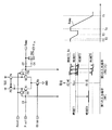
次に、比較部31と変更部18aの構成および比較部31の入力端子における電圧変化の詳細を説明する。図3は比較部31および変更部18aの具体的な回路構成の一例を示している。以下、本例の回路構成について説明する。
Next, the configuration of the
図3において、比較部31内の差動アンプは、ソースが共通に接続されたNMOSで構成されるトランジスタN1,N2と、これらトランジスタN1,N2の各ドレインと電源VDDとの間に接続され、ゲートが共通に接続されたPMOSで構成されるトランジスタP3,P4と、トランジスタN1,N2のソースに共通に接続されたノードとグランドGNDとの間に接続されたNMOSの電流源N5とで構成されている。
In FIG. 3, the differential amplifier in the
この差動アンプにおいて、トランジスタN1,N2の各ゲートとドレインとの間に、PMOSで構成されるトランジスタP6,P7がそれぞれ接続されている。これらトランジスタP6,P7は、各ゲートにLowアクティブのリセットパルスResetがタイミング制御部20から与えられることでON状態となり、トランジスタN1,N2の各ゲートとドレインとを短絡し、トランジスタN1,N2の各ゲートの電圧、即ち差動アンプの2つの入力端子IN1,IN2の電圧をリセットするリセット部として機能する。
In this differential amplifier, transistors P6 and P7 made of PMOS are connected between the gates and drains of the transistors N1 and N2, respectively. These transistors P6 and P7 are turned on when a low active reset pulse Reset is given to each gate from the
トランジスタN1,N2の各ゲートには、DCレベルをカットするための容量素子C1,C2の各一端がそれぞれ接続されている。容量素子C1(第1の容量素子)の他端には、撮像部2の各単位画素3から出力される画素信号Pixelが与えられる。容量素子C2の他端には、参照信号生成部16からの参照信号Rampが与えられる。
One end of each of capacitive elements C1 and C2 for cutting the DC level is connected to each gate of the transistors N1 and N2. A pixel signal Pixel output from each
変更部18aは容量素子C3(第2の容量素子)およびスイッチ素子SW1で構成されている。容量素子C3の一端はトランジスタN1のゲートに接続され、容量素子C3の他端はスイッチ素子SW1の第1の端子に接続される。スイッチ素子SW1の第2の端子は電圧源V1[n](n:1〜3)に接続され、スイッチ素子SW1の第3の端子は容量素子C1の他端に接続される。スイッチ素子SW1は、タイミング制御部20からの図示しない制御信号によって、第1の端子および第2の端子を短絡して電圧源V1[n]と容量素子C3の他端とが接続された状態と、第1の端子および第3の端子を短絡して容量素子C1の他端と容量素子C3の他端とが接続された状態との切替を行う。また、電流源N5のゲートには、電流値を制御するためのバイアス電圧Vbiasが与えられる。
The changing
以下、本例の動作について説明する。ここでは、電圧源V1[n]の電圧をV1[n]、リセットレベルの電圧をVR(ただし、VR<V1[n])、信号レベルの電圧をVS(ただし、VS≦VR)、容量素子C1の容量値をC1、容量素子C3の容量値をC3とする。また、容量素子C3およびスイッチ素子SW1を介して電圧源V1[n]に接続される差動アンプの第1の入力端子IN1を第1の入力端子IN1[n] (n:1〜3)とする。図3には、比較部31内の差動アンプの第1の入力端子IN1[n]および第2の入力端子IN2の電圧変化および参照信号Rampの波形が示されている。
The operation of this example will be described below. Here, the voltage of the voltage source V1 [n] is V 1 [n] , the reset level voltage is V R (where V R <V 1 [n] ), and the signal level voltage is V S (where V S ≦ V R ), the capacitance value of the capacitive element C1 is C 1 , and the capacitive value of the capacitive element C3 is C 3 . Further, the first input terminal IN1 of the differential amplifier connected to the voltage source V1 [n] through the capacitive element C3 and the switch element SW1 is replaced with the first input terminal IN1 [n] (n: 1 to 3). To do. FIG. 3 shows the voltage change of the first input terminal IN1 [n] and the second input terminal IN2 of the differential amplifier in the
単位画素3からの画素信号Pixelとしてリセットレベルが第1の入力端子IN1[n]に与えられ、参照信号生成部16から第2の入力端子IN2に与えられる参照信号Rampが安定した後、タイミング制御部20が比較部31の比較開始前にリセットパルスResetを活性化(Lowアクティブ)する。これにより、トランジスタP6,P7がON状態となってトランジスタN1,N2の各ゲートとドレインとを短絡し、これらトランジスタN1,N2の動作点をドレイン電圧として2つの入力端子の電圧がリセットされる。リセット動作中、容量素子C3の他端は、スイッチ素子SW1により電圧源V1[n]に接続されている。
After the reset level is given to the first input terminal IN1 [n] as the pixel signal Pixel from the
このリセットによって決定された動作点で、差動アンプの2つの入力端子の電圧、即ちトランジスタN1,N2の各ゲート電圧のオフセット成分がほぼキャンセルされる。即ち、差動アンプの2つの入力端子の電圧が、略同一の電圧VRSTになるようにリセットされる。この時点(時刻T1)で、第1の入力端子IN1[n]の電圧はVRST、第2の入力端子IN2の電圧はVRSTである。リセット後、トランジスタP6,P7はOFF状態となる。 At the operating point determined by this reset, the voltages at the two input terminals of the differential amplifier, that is, the offset components of the gate voltages of the transistors N1 and N2, are almost canceled. That is, the voltages at the two input terminals of the differential amplifier are reset so as to be substantially the same voltage VRST . At this time (time T1), the voltage of the first input terminal IN1 [n] is V RST and the voltage of the second input terminal IN2 is V RST . After reset, the transistors P6 and P7 are turned off.
続いて、スイッチ素子SW1が容量素子C3の他端を容量素子C1の他端に接続することで、画素信号Pixelが与えられる第1の入力端子IN1[n]の電圧、即ちトランジスタN1のゲート電圧が電圧VRSTから所定の電圧に低く変更される。容量素子C3の他端の電圧がV1[n]からVRに(VR - V1[n])だけ変化するため、この時点(時刻T2)で、第1の入力端子IN1[n]の電圧VIN1[n]は以下の(1)式となる。 Subsequently, the switching element SW1 connects the other end of the capacitive element C3 to the other end of the capacitive element C1, so that the voltage of the first input terminal IN1 [n] to which the pixel signal Pixel is applied, that is, the gate voltage of the transistor N1. Is changed from the voltage V RST to a predetermined voltage. Since the voltage at the other end of the capacitive element C3 changes from V 1 [n] to V R by (V R −V 1 [n] ), at this time (time T2), the first input terminal IN1 [n] The voltage V IN1 [n] is expressed by the following equation (1).

比較部31のリセット動作後に、比較部31を構成する差動アンプの2つの入力端子の電圧に多少のばらつきが残ったとしても、VR<V1[n]であるため、1回目の読出しに係る比較部31での比較開始時の第1の入力端子IN1[n]の電圧((1)式)は、第2の入力端子IN2の電圧(VRST)よりも低くなる。図3に示すように、参照信号Rampとして時間の経過とともに減少するランプ波を与えることで、比較部31の出力を比較動作中に確実に反転させ、比較部31による比較動作を保証することができる。
After the reset operation of the
時刻T2以降、第2の入力端子IN2に参照信号Rampとしてランプ波が与えられる。ランプ波が与えられた第2の入力端子IN2の電圧と、第1の入力端子IN1[n]の電圧とが略一致したタイミングで比較部31の比較出力が反転する。第2の入力端子IN2へのランプ波の入力が開始されてから所定の期間が経過した時点(時刻T3)で、参照信号生成部16はランプ波の生成を停止する。
After time T2, a ramp wave is applied as the reference signal Ramp to the second input terminal IN2. The comparison output of the
比較部31のリセット動作後、第1の入力端子IN1[1],IN1[2],IN1[3]に対して、(1)式の右辺第2項に係る電圧がオフセットとして印加される。電圧値V1[1],V1[2],V1[3] がそれぞれ異なり、各列の単位画素3から出力されるリセットレベルが略同一であるため、第1の入力端子IN1[1],IN1[2],IN1[3]に対して、それぞれ異なるオフセットが印加される。したがって、1回目の読出しに係る比較部31での比較開始時の第1の入力端子IN1[1],IN1[2],IN1[3]の電圧VIN1[1],VIN1[2],VIN1[3]((1)式)はそれぞれ異なる。これによって、1回目の読出しに係る比較部31での比較開始のタイミングが略同時であっても、比較終了のタイミングは領域39a,39b,39cのそれぞれの列AD変換部30の比較部31で異なる。このように、領域39a,39b,39cごとに比較部31が異なるタイミングで比較動作を終了することによって、電力集中が低減されるので、より高精度なAD変換を行うことができる。
After the reset operation of the
続いて、単位画素3からの画素信号Pixelとして信号レベルが第1の入力端子IN1[n]に与えられる。以下では、図4を用いて、信号レベルが入力された時点(時刻T4)での第1の入力端子IN1[n]の電圧を説明する。図4は、第1の入力端子IN1[n]の周辺の構成のみを抽出して示している。以下では、第1の入力端子IN1[n]とグランドGNDとの間の寄生容量CPを仮定して説明を行う。
Subsequently, the signal level is given to the first input terminal IN1 [n] as the pixel signal Pixel from the
スイッチ素子SW1によって容量素子C3の他端が容量素子C1の他端に接続された時点(時刻T2)で、画素信号Pixelとしてリセットレベルが与えられている容量素子C1の他端の電圧はVRである。また、画素信号Pixelとして信号レベルが入力された時点(時刻T4)で、容量素子C1の他端の電圧はVSとなる。時刻T2から時刻T4までの容量素子C1の他端の電圧の変化をΔV1とすると、ΔV1は以下の(2)式となる。
ΔV1 = VS - VR ・・・(2)
When the other end of the capacitive element C3 is connected to the other end of the capacitive element C1 by the switch element SW1 (time T2), the voltage at the other end of the capacitive element C1 to which the reset level is given as the pixel signal Pixel is V R It is. At the time (time T4) when the signal level is input as the pixel signal Pixel, the voltage at the other end of the capacitive element C1 becomes V S. Assuming that the change in voltage at the other end of the capacitive element C1 from time T2 to time T4 is ΔV1, ΔV1 is expressed by the following equation (2).
ΔV1 = V S -V R (2)
時刻T2から時刻T4までの間、トランジスタP6がOFF状態であるため、容量素子C1,C3および寄生容量CPに蓄積されている電荷量は保持される。このため、時刻T2から時刻T4までの第1の入力端子IN1[n]の電圧の変化をΔV2とすると、ΔV2は以下の(3)式となる。尚、容量素子C1と容量素子C3は並列に接続されており、この並列に接続された容量素子C1と容量素子C3を合成した容量値が(3)式のCCである。また、(3)式において、CPは寄生容量CPの容量値である。 Since the transistor P6 is in the OFF state from time T2 to time T4, the charge amount accumulated in the capacitive elements C1 and C3 and the parasitic capacitance CP is held. Therefore, if the change in voltage of the first input terminal IN1 [n] from time T2 to time T4 is ΔV2, ΔV2 is expressed by the following equation (3). Note that the capacitive element C1 and the capacitive element C3 are connected in parallel, and the capacitance value obtained by synthesizing the capacitive element C1 and the capacitive element C3 connected in parallel is CC in the equation (3). In Equation (3), C P is the capacitance value of the parasitic capacitance CP.
CCに比べてCPを無視できる場合(CC>> CP)、ΔV2=ΔV1となる。時刻T2における第1の入力端子IN1[n]の電圧は(1)式であるので、時刻T4における第1の入力端子IN1[n]の電圧VIN1[1]は以下の(4)式となる。 If you can ignore the C P compared to C C (C C >> C P ), the ΔV2 = ΔV1. Since the voltage of the first input terminal IN1 [n] at the time T2 is the expression (1), the voltage V IN1 [1] of the first input terminal IN1 [n] at the time T4 is the following expression (4): Become.
VR<V1[n]かつVS≦VRであるため、2回目の読出しに係る比較部31での比較開始時の第1の入力端子IN1[n]の電圧((4)式)は、第2の入力端子IN2の電圧(VRST)よりも低くなる。図3に示すように、参照信号Rampとして時間の経過とともに減少するランプ波を与えることで、比較部31の出力を比較動作中に確実に反転させ、比較部31による比較動作を保証することができる。
Since V R <V 1 [n] and V S ≦ V R , the voltage of the first input terminal IN1 [n] at the start of comparison in the
時刻T4以降、第2の入力端子IN2に参照信号Rampとしてランプ波が与えられる。ランプ波が与えられた第2の入力端子IN2の電圧と、第1の入力端子IN1[n]の電圧とが略一致したタイミングで比較部31の比較出力が反転する。第2の入力端子IN2へのランプ波の入力が開始されてから所定の期間が経過した時点(時刻T5)で、参照信号生成部16はランプ波の生成を停止する。1回目の読出し時に計測部32がダウンカウントモードで計測を行い、2回目の読出し時に計測部32がアップカウントモードで計測を行うため、計測部32の計測値として、(4)式の右辺第3項に係る計測値が得られる。(4)式では、右辺第3項の係数が1であるので、容量素子C3を設けたことに起因するゲイン低下のないAD変換動作が可能となる。
After time T4, a ramp wave is applied as the reference signal Ramp to the second input terminal IN2. The comparison output of the
前述したように、電圧値V1[1],V1[2],V1[3] はそれぞれ異なる。また、各列の単位画素3から出力されるリセットレベルは略同一であり、信号レベルは異なることが多い。このため、2回目の読出しに係る比較部31での比較開始時の第1の入力端子IN1[1],IN1[2],IN1[3]の電圧VIN1[1],VIN1[2],VIN1[3]((4)式)はそれぞれ異なることが多い。これによって、2回目の読出しに係る比較部31での比較開始のタイミングが略同時であっても、比較終了のタイミングは領域39a,39b,39cのそれぞれの列AD変換部30の比較部31で異なる。このように、領域39a,39b,39cごとに比較部31が異なるタイミングで比較動作を終了することによって、電力集中が低減されるので、より高精度なAD変換を行うことができる。
As described above, the voltage values V 1 [1] , V 1 [2] , and V 1 [3] are different. The reset levels output from the
上述したように、本実施形態によれば、トランジスタP6,P7によるリセット動作後に、第1の入力端子IN1と第2の入力端子IN2との電圧差が、比較部31による比較動作を保証する電圧となるように、変更部18a(容量素子C3およびスイッチ素子SW1)が第1の入力端子IN1の電圧をより低い電圧に変更することによって、比較部31が参照信号Rampと画素信号Pixelとの比較動作を確実に行うことができる。
As described above, according to the present embodiment, after the reset operation by the transistors P6 and P7, the voltage difference between the first input terminal IN1 and the second input terminal IN2 guarantees the comparison operation by the
また、領域39a,39b,39cごとに、比較部31の第1の入力端子IN1に異なるオフセットが印加されるので、領域39a,39b,39cのそれぞれの列AD変換部30における各比較部31が略同時に比較を開始した場合でも、異なるタイミングで各比較部31に比較を終了させることが可能となる。これによって、電力集中が低減されるので、より高精度なAD変換を行うことができる。
In addition, since different offsets are applied to the first input terminal IN1 of the
また、容量素子C3の他端が、スイッチ素子SW1を介して、電圧源V1[n]と、単位画素3からのアナログ信号が供給される垂直信号線13とに接続されるように変更部18aを構成することによって、容量素子C3を設けたことに起因するゲイン低下のないAD変換動作が可能となる。
Further, the changing
(第2の実施形態)
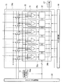
次に、本発明の第2の実施形態を説明する。本実施形態では、変更部が第1の実施形態と異なる。図5は、列AD変換部30および変更部18bを含むカラム処理部15の構成の一例を示している。他の構成については、図1に示した構成と略同様であるので説明を省略する。
(Second embodiment)
Next, a second embodiment of the present invention will be described. In the present embodiment, the changing unit is different from that of the first embodiment. FIG. 5 shows an example of the configuration of the
変更部18bは容量素子およびスイッチ素子で構成されている。容量素子の一端は比較部31の第2の入力端子に接続され、容量素子の他端は、スイッチ素子を介して、電圧源V1[n](n:1〜3)(第1の電圧源)と、参照信号生成部16からの参照信号Ramp(第2の電圧源)が供給される参照信号線とに接続される。電圧源V1[1]は、領域39aの列AD変換部30に対応する変更部18bに電源電圧(電圧値:V1[1])を供給する。電圧源V1[2]は、領域39bの列AD変換部30に対応する変更部18bに電源電圧(電圧値:V1[2])を供給する。電圧源V1[3]は、領域39cの列AD変換部30に対応する変更部18bに電源電圧(電圧値:V1[3])を供給する。各電圧値V1[n](n:1〜3)の大小関係は、例えばV1[1]<V1[2]<V1[3]である。尚、これらは一例であって、これに限る必要はない。
The changing
以下では、本例の動作のうち、第1の実施形態と異なる部分を中心に説明する。第1の実施形態と同様に、単位画素3ではリセットレベルと信号レベルとが出力される。
In the following, the operation of this example will be described with a focus on the differences from the first embodiment. As in the first embodiment, the
<1回目の読出し>
任意の画素行の単位画素3から垂直信号線13への1回目の読出しが安定した後、比較部31のリセット動作が行われる。続いて、変更部18bは、参照信号Rampが与えられた比較部31の第2の入力端子の電圧を、リセットレベルよりも高い所定の電圧に変更する。その後、タイミング制御部20は、参照信号生成部16に対して、ランプ波生成の制御データを供給する。これを受けて参照信号生成部16は、比較部31の第2の入力端子に与える比較電圧として、波形が全体として時間的にランプ状に変化する参照信号Rampを出力する。比較部31は、参照信号生成部16からの参照信号Rampが与えられた第2の入力端子の電圧と、リセットレベルが与えられた第1の入力端子の電圧とを比較し、双方の電圧が略一致したときに、比較出力を反転させる。
<First reading>
After the first reading from the
計測部32は、比較部31での比較開始に基づいてダウンカウントモードで計測を開始し、比較部31の比較出力が反転した時点の計測値を保持する。つまり、計測部32は、リセットレベルに応じたデジタルデータを保持する。タイミング制御部20は、所定の期間を経過すると、参照信号生成部16への制御データの供給と、基準クロックの出力とを停止する。これにより、参照信号生成部16は、参照信号Rampの生成を停止する。
The
<2回目の読出し>
続いて、2回目の読出し時には、単位画素3毎の入射光量に応じた信号レベルが読み出される。この2回目の読出し時には、比較部31のリセット動作および変更部18bによる変更動作は行わない。
<Second reading>
Subsequently, in the second reading, a signal level corresponding to the incident light amount for each
任意の画素行の単位画素3から垂直信号線13への2回目の読出しが安定した後、タイミング制御部20は、参照信号生成部16に対して、ランプ波生成の制御データを供給する。これを受けて参照信号生成部16は参照信号Rampを出力する。比較部31は、参照信号生成部16からの参照信号Rampが与えられた第2の入力端子の電圧と、信号レベルが与えられた第1の入力端子の電圧とを比較し、双方の電圧が略一致したときに、比較出力を反転させる。
After the second reading from the
計測部32は、比較部31での比較開始に基づいてアップカウントモードで計測を開始し、比較部31の比較出力が反転した時点の計測値を保持する。つまり、計測部32は、信号レベルからリセットレベルを減算した信号成分に応じたデジタルデータを保持する。タイミング制御部20は、所定の期間を経過すると、参照信号生成部16への制御データの供給と、基準クロックの出力とを停止する。これにより、参照信号生成部16は、参照信号Rampの生成を停止する。
The
次に、比較部31と変更部18bの構成および比較部31の入力端子における電圧変化の詳細を説明する。図6は、比較部31および変更部18bの具体的な回路構成の一例を示している。以下、本例の回路構成について説明する。以下では、図5に示した構成と異なる構成についてのみ説明する。
Next, the configuration of the
変更部18bは容量素子C4(第2の容量素子)およびスイッチ素子SW2で構成されている。容量素子C4の一端はトランジスタN2のゲートに接続され、容量素子C4の他端はスイッチ素子SW2の第1の端子に接続される。スイッチ素子SW2の第2の端子は電圧源V1[n](n:1〜3)に接続され、スイッチ素子SW2の第3の端子は容量素子C2の他端に接続される。スイッチ素子SW2は、第1の端子および第2の端子を短絡して電圧源V1[n]と容量素子C4の他端とが接続された状態と、第1の端子および第3の端子を短絡して容量素子C2の他端と容量素子C4の他端とが接続された状態との切替を行う。
The changing
以下、本例の動作について説明する。ここでは、電圧源V1[n]の電圧をV1[n]、リセットレベルの電圧をVR、信号レベルの電圧をVS(ただし、VS≦VR)、容量素子C2の容量値をC2、容量素子C4の容量値をC4とする。また、容量素子C4およびスイッチ素子SW2を介して電圧源V1[n]に接続される差動アンプの第2の入力端子IN2を第2の入力端子IN2[n] (n:1〜3)とする。図6には、比較部31内の差動アンプの第1の入力端子IN1および第2の入力端子IN2[n]の電圧変化および参照信号Rampの波形が示されている。
The operation of this example will be described below. Here, the voltage of the voltage source V1 [n] is V 1 [n] , the reset level voltage is V R , the signal level voltage is V S (where V S ≦ V R ), and the capacitance value of the capacitive element C2 is C 2, the capacitance of the capacitor C4 and C 4. Further, the second input terminal IN2 of the differential amplifier connected to the voltage source V1 [n] through the capacitive element C4 and the switch element SW2 is replaced with the second input terminal IN2 [n] (n: 1 to 3). To do. FIG. 6 shows the voltage change of the first input terminal IN1 and the second input terminal IN2 [n] of the differential amplifier in the
単位画素3からの画素信号Pixelとしてリセットレベルが第1の入力端子IN1に与えられ、参照信号生成部16から第2の入力端子IN2[n]に与えられる参照信号Rampが安定した後、タイミング制御部20が比較部31の比較開始前にリセットパルスResetを活性化(Lowアクティブ)する。これにより、トランジスタP6,P7がON状態となってトランジスタN1,N2の各ゲートとドレインとを短絡し、これらトランジスタN1,N2の動作点をドレイン電圧として2つの入力端子の電圧がリセットされる。リセット動作中、容量素子C4の他端は、スイッチ素子SW2により電圧源V1[n]に接続されている。
After the reset level is given to the first input terminal IN1 as the pixel signal Pixel from the
このリセットによって決定された動作点で、差動アンプの2つの入力端子の電圧、即ちトランジスタN1,N2の各ゲート電圧のオフセット成分がほぼキャンセルされる。即ち、差動アンプの2つの入力端子の電圧が、略同一の電圧VRSTになるようにリセットされる。この時点(時刻T1)で、第1の入力端子IN1の電圧はVRST、第2の入力端子IN2[n]の電圧はVRSTである。リセット後、トランジスタP6,P7はOFF状態となる。 At the operating point determined by this reset, the voltages at the two input terminals of the differential amplifier, that is, the offset components of the gate voltages of the transistors N1 and N2, are almost canceled. That is, the voltages at the two input terminals of the differential amplifier are reset so as to be substantially the same voltage VRST . At this time (time T1), the voltage at the first input terminal IN1 is V RST and the voltage at the second input terminal IN2 [n] is V RST . After reset, the transistors P6 and P7 are turned off.
続いて、スイッチ素子SW2が容量素子C4の他端を容量素子C2の他端に接続することで、参照信号Rampが与えられる第2の入力端子IN2[n]の電圧、即ちトランジスタN2のゲート電圧が電圧VRSTから所定の電圧に高く変更される。この時点(時刻T2)での参照信号Rampの電圧をVRamp(0)とすると、容量素子C4の他端の電圧がV1[n]からVRamp(0)に(VRamp(0) - V1[n])だけ変化するため、この時点(時刻T2)で、第2の入力端子IN2[n]の電圧VIN2は以下の(5)式となる。ここで、電圧源V1[n]の電圧V1[n]と参照信号Rampの電圧VRamp(0)との関係は、V1[n]<VRamp(0)である。 Subsequently, the switching element SW2 connects the other end of the capacitive element C4 to the other end of the capacitive element C2, so that the voltage of the second input terminal IN2 [n] to which the reference signal Ramp is applied, that is, the gate voltage of the transistor N2 Is increased from the voltage V RST to a predetermined voltage. If the voltage of the reference signal Ramp at this time (time T2) is V Ramp (0), the voltage at the other end of the capacitive element C4 changes from V 1 [n] to V Ramp (0) (V Ramp (0) − V 1 [n] ) changes, and at this time (time T2), the voltage V IN2 of the second input terminal IN2 [n] is expressed by the following equation (5). Here, the relationship between the voltage V 1 [n] of the voltage source V 1 [n] and the voltage V Ramp (0) of the reference signal Ramp is V 1 [n] <V Ramp (0).
比較部31のリセット動作後に、比較部31を構成する差動アンプの2つの入力端子の電圧に多少のばらつきが残ったとしても、V1[n]<VRamp(0)であるため、1回目の読出しに係る比較部31での比較開始時の第2の入力端子IN2[n]の電圧((5)式)は第1の入力端子IN1の電圧(VRST)よりも高くなる。図6に示すように、参照信号Rampとして時間の経過とともに減少するランプ波を与えることで、比較部31の出力を比較動作中に確実に反転させ、比較部31による比較動作を保証することができる。
Even after the reset operation of the
時刻T2以降、第2の入力端子IN2[n]に参照信号Rampとしてランプ波が与えられる。以下では、図7を用いて、ランプ波が与えられた第2の入力端子IN2[n]の電圧を説明する。図7は、第2の入力端子IN2[n]の周辺の構成のみを抽出して示している。以下では、第2の入力端子IN2[n]とグランドGNDとの間の寄生容量CPを仮定して説明を行う。 After time T2, a ramp wave is given as the reference signal Ramp to the second input terminal IN2 [n]. Hereinafter, the voltage of the second input terminal IN2 [n] to which the ramp wave is applied will be described with reference to FIG. FIG. 7 shows only the configuration around the second input terminal IN2 [n]. Hereinafter, description will be made assuming a parasitic capacitance CP between the second input terminal IN2 [n] and the ground GND.
容量素子C2の他端に与えられるランプ波の電圧がVRamp(0)からVRamp(t)まで(VRamp(t) - VRamp(0))だけ変化した場合の容量素子C2の他端の電圧の変化をΔV3とすると、ΔV3は以下の(6)式となる。
ΔV3 = VRamp(t) - VRamp(0) ・・・(6)
The other end of the capacitive element C2 when the voltage of the ramp wave applied to the other end of the capacitive element C2 changes from V Ramp (0) to V Ramp (t) (V Ramp (t)-V Ramp (0)) Assuming that the change in voltage is ΔV3, ΔV3 is expressed by the following equation (6).
ΔV3 = V Ramp (t)-V Ramp (0) (6)
時刻T2から時刻T4までの間、トランジスタP7がOFF状態であるため、容量素子C2,C4および寄生容量CPに蓄積されている電荷量は保持される。このため、容量素子C2の他端に与えられるランプ波の電圧がVRamp(0)からVRamp(t)まで(VRamp(t) - VRamp(0))だけ変化した場合の第2の入力端子IN2[n]の電圧の変化をΔV4とすると、ΔV4は以下の(7)式となる。尚、容量素子C2と容量素子C4は並列に接続されており、この並列に接続された容量素子C2と容量素子C4を合成した容量値が(7)式のCCである。また、(7)式において、CPは寄生容量CPの容量値である。 Since the transistor P7 is in the OFF state from time T2 to time T4, the charge amount accumulated in the capacitive elements C2 and C4 and the parasitic capacitance CP is retained. Therefore, the second voltage when the voltage of the ramp wave applied to the other end of the capacitive element C2 changes from V Ramp (0) to V Ramp (t) (V Ramp (t)-V Ramp (0)). When the change in voltage at the input terminal IN2 [n] is ΔV4, ΔV4 is expressed by the following equation (7). Note that the capacitive element C2 and the capacitive element C4 are connected in parallel, and the capacitance value obtained by synthesizing the capacitive element C2 and the capacitive element C4 connected in parallel is CC in the equation (7). In Equation (7), C P is a capacitance value of the parasitic capacitance CP.
CCに比べてCPを無視できる場合(CC>> CP)、ΔV4=ΔV3となる。時刻T2における第2の入力端子IN2[n]の電圧は(5)式であるので、時刻T2以降の第2の入力端子IN2[n]の電圧VIN2[n]は以下の(8)式となる。(8)式では、右辺第3項の係数が1であるので、容量素子C4を設けている本実施形態においても、参照信号Rampの時間変化の割合(参照信号Rampの傾き)を、第1の実施形態における参照信号Rampの時間変化の割合と同等に保つことが可能となる。 If you can ignore the C P compared to C C (C C >> C P ), the ΔV4 = ΔV3. Since the voltage of the second input terminal IN2 [n] at time T2 is the expression (5), the voltage V IN2 [n] of the second input terminal IN2 [n] after the time T2 is the following expression (8) It becomes. In the equation (8), since the coefficient of the third term on the right side is 1, also in the present embodiment in which the capacitive element C4 is provided, the rate of change over time of the reference signal Ramp (the slope of the reference signal Ramp) is expressed as follows. It is possible to keep the reference signal Ramp equal to the rate of change with time in the embodiment.
ランプ波が与えられた第2の入力端子IN2[n]と、第1の入力端子IN1の電圧とが略一致したタイミングで比較部31の比較出力が反転する。第2の入力端子IN2[n]へのランプ波の入力が開始されてから所定の期間が経過した時点(時刻T3)で、参照信号生成部16はランプ波の生成を停止する。
The comparison output of the
比較部31のリセット動作後、第2の入力端子IN2[1],IN2[2],IN2[3]に対して、(5)式の右辺第2項に係る電圧がオフセットとして印加される。電圧値V1[1],V1[2],V1[3] がそれぞれ異なり、各列の比較部31の第2の入力端子IN2[n]に与えられる参照信号Rampが略同一であるため、第2の入力端子IN2[1],IN2[2],IN2[3]に対して、それぞれ異なるオフセットが印加される。したがって、1回目の読出しに係る比較部31での比較開始時の第2の入力端子IN2[1],IN2[2],IN2[3]の電圧VIN2[1],VIN2[2],VIN2[3]((5)式)はそれぞれ異なる。これによって、1回目の読出しに係る比較部31での比較開始のタイミングが略同時であっても、比較終了のタイミングは領域39a,39b,39cのそれぞれの列AD変換部30の比較部31で異なる。このように、領域39a,39b,39cごとに比較部31が異なるタイミングで比較動作を終了することによって、電力集中が低減されるので、より高精度なAD変換を行うことができる。
After the reset operation of the
続いて、単位画素3からの画素信号Pixelとして信号レベルが第1の入力端子IN1に与えられる。スイッチ素子SW2によって容量素子C4の他端が容量素子C2の他端に接続された時点(時刻T2)で、画素信号Pixelとしてリセットレベルが与えられている容量素子C1の他端の電圧はVRである。また、画素信号Pixelとして信号レベルが入力された時点(時刻T4)で、容量素子C1の他端の電圧はVSとなる。したがって、時刻T4における第1の入力端子IN1の電圧VIN1は以下の(9)式となる。
VIN1 = VRST +(VS - VR) ・・・(9)
Subsequently, a signal level is given to the first input terminal IN1 as a pixel signal Pixel from the
V IN1 = V RST + (V S -V R ) (9)
2回目の読出しに係る時刻T4において、参照信号Rampが与えられる第2の入力端子IN2[n]の電圧は、前述した(5)式となる。(5)式においてV1[n]<VRamp(0)であり、(9)式においてVS≦VRであるため、(5)式の電圧VIN2[n]は(9)式の電圧VIN1よりも高くなる。即ち、2回目の読出しに係る比較部31での比較開始時の第2の入力端子IN2[n]の電圧は第1の入力端子IN1の電圧よりも高くなる。図6に示すように、参照信号Rampとして時間の経過とともに減少するランプ波を与えることで、比較部31の出力を比較動作中に確実に反転させ、比較部31による比較動作を保証することができる。
At time T4 related to the second reading, the voltage of the second input terminal IN2 [n] to which the reference signal Ramp is applied is expressed by the above-described equation (5). Since V 1 [n] <V Ramp (0) in equation (5) and V S ≦ V R in equation (9), voltage V IN2 [n] in equation (5) is It becomes higher than the voltage V IN1 . That is, the voltage of the second input terminal IN2 [n] at the start of the comparison in the
時刻T4以降、第2の入力端子IN2[n]に参照信号Rampとしてランプ波が与えられる。第2の入力端子IN2[n]にランプ波が与えられた時点以降の第2の入力端子IN2[n]の電圧VIN2[n]は、前述した(8)式となる。ランプ波が与えられた第2の入力端子IN2[n]の電圧と、第1の入力端子IN1の電圧とが略一致したタイミングで比較部31の比較出力が反転する。第2の入力端子IN2[n]へのランプ波の入力が開始されてから所定の期間が経過した時点(時刻T5)で、参照信号生成部16はランプ波の生成を停止する。1回目の読出し時に計測部32がダウンカウントモードで計測を行い、2回目の読出し時に計測部32がアップカウントモードで計測を行うため、計測部32の計測値として、(9)式の右辺第2項(VS - VR)に係る計測値が得られる。
After time T4, a ramp wave is applied as the reference signal Ramp to the second input terminal IN2 [n]. The voltage V IN2 [n] of the second input terminal IN2 [n] after the point in time when the ramp wave is applied to the second input terminal IN2 [n] is expressed by the above-described equation (8). The comparison output of the
前述したように、2回目の読出しに係る比較部31での比較開始時の第2の入力端子IN2[1],IN2[2],IN2[3]の電圧VIN2[1],VIN2[2],VIN2[3]は(5)式となり、それぞれ異なる。これによって、2回目の読出しに係る比較部31での比較開始のタイミングが略同時であっても、比較終了のタイミングは領域39a,39b,39cのそれぞれの列AD変換部30の比較部31で異なる。このように、領域39a,39b,39cごとに比較部31が異なるタイミングで比較動作を終了することによって、電力集中が低減されるので、より高精度なAD変換を行うことができる。
As described above, the voltages V IN2 [1] and V IN2 [ at the second input terminals IN2 [1], IN2 [2], and IN2 [3] at the start of comparison in the
上述したように、本実施形態によれば、トランジスタP6,P7によるリセット動作後に、第1の入力端子IN1と第2の入力端子IN2との電圧差が、比較部31による比較動作を保証する電圧となるように、変更部18b(容量素子C4およびスイッチ素子SW2)が第2の入力端子IN2の電圧をより高い電圧に変更することによって、比較部31が参照信号Rampと画素信号Pixelとの比較動作を確実に行うことができる。
As described above, according to the present embodiment, after the reset operation by the transistors P6 and P7, the voltage difference between the first input terminal IN1 and the second input terminal IN2 guarantees the comparison operation by the
また、領域39a,39b,39cごとに、比較部31の第2の入力端子IN2に異なるオフセットが印加されるので、領域39a,39b,39cのそれぞれの列AD変換部30における各比較部31が略同時に比較を開始した場合でも、異なるタイミングで各比較部31に比較を終了させることが可能となる。これによって、電力集中が低減されるので、より高精度なAD変換を行うことができる。
Further, since different offsets are applied to the second input terminal IN2 of the
また、容量素子C4の他端が、スイッチ素子SW2を介して、電圧源V1[n]と、参照信号生成部16からの参照信号Rampが供給される参照信号線とに接続されるように変更部18bを構成することによって、参照信号Rampの時間変化の割合を、第1の実施形態における参照信号Rampの時間変化の割合と同等に保つことが可能となる。
In addition, the other end of the capacitive element C4 is changed to be connected to the voltage source V1 [n] and the reference signal line to which the reference signal Ramp from the reference
(第3の実施形態)
次に、本発明の第3の実施形態を説明する。本実施形態では、変更部が第1の実施形態と異なる。図8は、列AD変換部30および変更部18cを含むカラム処理部15の構成の一例を示している。他の構成については、図1に示した構成と略同様であるので説明を省略する。
(Third embodiment)
Next, a third embodiment of the present invention will be described. In the present embodiment, the changing unit is different from that of the first embodiment. FIG. 8 shows an example of the configuration of the
変更部18cは容量素子およびスイッチ素子で構成されている。容量素子の一端は比較部31の第1の入力端子に接続され、容量素子の他端は、スイッチ素子を介して、電圧源V1(第1の電圧源)と、単位画素3からのアナログ信号(第2の電圧源)が供給される垂直信号線13とに接続される。電圧源V1は、変更部18cに電源電圧(電圧値:V1)を供給する。変更部18cが有する容量素子を容量素子C3[n](n:1〜3)とし、その容量値をC3[n](n:1〜3)とする。領域39aの列AD変換部30に対応する変更部18cの容量素子C3[1]の容量値はC3[1]である。領域39bの列AD変換部30に対応する変更部18cの容量素子C3[2]の容量値はC3[2]である。領域39cの列AD変換部30に対応する変更部18cの容量素子C3[3]の容量値はC3[3]である。各容量値C3[n]の大小関係は、例えばC3[1]<C3[2]<C3[3]である。尚、これらは一例であって、これに限る必要はない。
The changing
1回目の読出し時および2回目の読出し時における列AD変換部30および変更部18cの動作は、第1の実施形態における列AD変換部30および変更部18aの動作と同様であるので、説明を省略する。
Since the operations of the column
次に、比較部31と変更部18cの構成および比較部31の入力端子における電圧変化の詳細を説明する。図9は比較部31および変更部18cの具体的な回路構成の一例を示している。以下、本例の回路構成について、第1の実施形態と異なる部分のみを説明する。
Next, the configuration of the
変更部18cは容量素子C3[n](第2の容量素子)およびスイッチ素子SW1で構成されている。容量素子C3[n]の一端はトランジスタN1のゲートに接続され、容量素子C3[n]の他端はスイッチ素子SW1の第1の端子に接続される。スイッチ素子SW1の第2の端子は電圧源V1に接続され、スイッチ素子SW1の第3の端子は容量素子C1の他端に接続される。スイッチ素子SW1は、タイミング制御部20からの図示しない制御信号によって、第1の端子および第2の端子を短絡して電圧源V1と容量素子C3[n]の他端とが接続された状態と、第1の端子および第3の端子を短絡して容量素子C1の他端と容量素子C3[n]の他端とが接続された状態との切替を行う。
The changing
例えば、容量素子C3[n]を、同一の容量値を有する複数の単位容量素子で構成し、その接続を制御することで容量値を変化させても構わない。尚、図9に示す構成の場合、容量素子C1を、領域毎に異なる容量値を有する容量素子C1[n](n:1〜3)として構成し、容量素子C1[n]と容量素子C3[n]の容量値を合計した容量値が一定となることが望ましい。 For example, the capacitive element C3 [n] may be configured by a plurality of unit capacitive elements having the same capacitance value, and the capacitance value may be changed by controlling the connection. In the case of the configuration illustrated in FIG. 9, the capacitive element C1 is configured as a capacitive element C1 [n] (n: 1 to 3) having different capacitance values for each region, and the capacitive element C1 [n] and the capacitive element C3 It is desirable that the total capacitance value of [n] is constant.
以下、本例の動作について説明する。ここでは、電圧源V1の電圧をV1、リセットレベルの電圧をVR(ただし、VR<V1)、信号レベルの電圧をVS(ただし、VS≦VR)、容量素子C1の容量値をC1、容量素子C3[n]の容量値をC3[n]とする。また、容量素子C3[n]およびスイッチ素子SW1を介して電圧源V1に接続される差動アンプの第1の入力端子IN1を第1の入力端子IN1[n] (n:1〜3)とする。図9には、比較部31内の差動アンプの第1の入力端子IN1[n]および第2の入力端子IN2の電圧変化および参照信号Rampの波形が示されている。
The operation of this example will be described below. Here, the voltage of the voltage source V1 is V 1 , the reset level voltage is V R (where V R <V 1 ), the signal level voltage is V S (where V S ≦ V R ), and the capacitance element C1 Assume that the capacitance value is C 1 and the capacitance value of the capacitive element C3 [n] is C 3 [n] . Further, the first input terminal IN1 of the differential amplifier connected to the voltage source V1 via the capacitive element C3 [n] and the switch element SW1 is replaced with the first input terminal IN1 [n] (n: 1 to 3). To do. FIG. 9 shows the voltage change of the first input terminal IN1 [n] and the second input terminal IN2 of the differential amplifier in the
単位画素3からの画素信号Pixelとしてリセットレベルが第1の入力端子IN1[n]に与えられ、参照信号生成部16から第2の入力端子IN2に与えられる参照信号Rampが安定した後、タイミング制御部20が比較部31の比較開始前にリセットパルスResetを活性化(Lowアクティブ)する。これにより、トランジスタP6,P7がON状態となってトランジスタN1,N2の各ゲートとドレインとを短絡し、これらトランジスタN1,N2の動作点をドレイン電圧として2つの入力端子の電圧がリセットされる。リセット動作中、容量素子C3[n]の他端は、スイッチ素子SW1により電圧源V1に接続されている。
After the reset level is given to the first input terminal IN1 [n] as the pixel signal Pixel from the
このリセットによって決定された動作点で、差動アンプの2つの入力端子の電圧、即ちトランジスタN1,N2の各ゲート電圧のオフセット成分がほぼキャンセルされる。即ち、差動アンプの2つの入力端子の電圧が、略同一の電圧VRSTになるようにリセットされる。この時点(時刻T1)で、第1の入力端子IN1[n]の電圧はVRST、第2の入力端子IN2の電圧はVRSTである。リセット後、トランジスタP6,P7はOFF状態となる。 At the operating point determined by this reset, the voltages at the two input terminals of the differential amplifier, that is, the offset components of the gate voltages of the transistors N1 and N2, are almost canceled. That is, the voltages at the two input terminals of the differential amplifier are reset so as to be substantially the same voltage VRST . At this time (time T1), the voltage of the first input terminal IN1 [n] is V RST and the voltage of the second input terminal IN2 is V RST . After reset, the transistors P6 and P7 are turned off.
続いて、スイッチ素子SW1が容量素子C3の他端を容量素子C1の他端に接続することで、画素信号Pixelが与えられる第1の入力端子IN1[n]の電圧、即ちトランジスタN1のゲート電圧が電圧VRSTから所定の電圧に低く変更される。この時点(時刻T2)での第1の入力端子IN1[n]の電圧VIN1[n]は、第1の実施形態における(1)式と同様に、以下の(10)式となる。 Subsequently, the switching element SW1 connects the other end of the capacitive element C3 to the other end of the capacitive element C1, so that the voltage of the first input terminal IN1 [n] to which the pixel signal Pixel is applied, that is, the gate voltage of the transistor N1. Is changed from the voltage V RST to a predetermined voltage. The voltage V IN1 [n] of the first input terminal IN1 [n] at this time (time T2) is expressed by the following expression (10), similar to the expression (1) in the first embodiment.
比較部31のリセット動作後に、比較部31を構成する差動アンプの2つの入力端子の電圧に多少のばらつきが残ったとしても、VR<V1であるため、1回目の読出しに係る比較部31での比較開始時の第1の入力端子IN1[n]の電圧((10)式)は、第2の入力端子IN2の電圧(VRST)よりも低くなる。図9に示すように、参照信号Rampとして時間の経過とともに減少するランプ波を与えることで、比較部31の出力を比較動作中に確実に反転させ、比較部31による比較動作を保証することができる。
Even after the reset operation of the
時刻T2以降、第2の入力端子IN2に参照信号Rampとしてランプ波が与えられる。ランプ波が与えられた第2の入力端子IN2の電圧と、第1の入力端子IN1[n]の電圧とが略一致したタイミングで比較部31の比較出力が反転する。第2の入力端子IN2へのランプ波の入力が開始されてから所定の期間が経過した時点(時刻T3)で、参照信号生成部16はランプ波の生成を停止する。
After time T2, a ramp wave is applied as the reference signal Ramp to the second input terminal IN2. The comparison output of the
比較部31のリセット動作後、第1の入力端子IN1[1],IN1[2],IN1[3]に対して、(10)式の右辺第2項に係る電圧がオフセットとして印加される。容量値C3[1],C3[2],C3[3]がそれぞれ異なり、各列の単位画素3から出力されるリセットレベルが略同一であるため、第1の入力端子IN1[1],IN1[2],IN1[3]に対して、それぞれ異なるオフセットが印加される。したがって、1回目の読出しに係る比較部31での比較開始時の第1の入力端子IN1[1],IN1[2],IN1[3]の電圧VIN1[1],VIN1[2],VIN1[3]((10)式)はそれぞれ異なる。これによって、1回目の読出しに係る比較部31での比較開始のタイミングが略同時であっても、比較終了のタイミングは領域39a,39b,39cのそれぞれの列AD変換部30の比較部31で異なる。このように、領域39a,39b,39cごとに比較部31が異なるタイミングで比較動作を終了することによって、電力集中が低減されるので、より高精度なAD変換を行うことができる。
After the reset operation of the
続いて、単位画素3からの画素信号Pixelとして信号レベルが第1の入力端子IN1[n]に与えられる。この時点(時刻T4)での第1の入力端子IN1[n]の電圧VIN1[1]は、第1の実施形態における(4)式と同様に、以下の(11)式となる。
Subsequently, the signal level is given to the first input terminal IN1 [n] as the pixel signal Pixel from the
VR<V1かつVS≦VRであるため、2回目の読出しに係る比較部31での比較開始時の第1の入力端子IN1[n]の電圧((11)式)は、第2の入力端子IN2の電圧(VRST)よりも低くなる。図9に示すように、参照信号Rampとして時間の経過とともに減少するランプ波を与えることで、比較部31の出力を比較動作中に確実に反転させ、比較部31による比較動作を保証することができる。
Since V R <V 1 and V S ≦ V R , the voltage of the first input terminal IN1 [n] at the start of comparison in the
時刻T4以降、第2の入力端子IN2に参照信号Rampとしてランプ波が与えられる。ランプ波が与えられた第2の入力端子IN2の電圧と、第1の入力端子IN1[n]の電圧とが略一致したタイミングで比較部31の比較出力が反転する。第2の入力端子IN2へのランプ波の入力が開始されてから所定の期間が経過した時点(時刻T5)で、参照信号生成部16はランプ波の生成を停止する。1回目の読出し時に計測部32がダウンカウントモードで計測を行い、2回目の読出し時に計測部32がアップカウントモードで計測を行うため、計測部32の計測値として、(11)式の右辺第3項に係る計測値が得られる。したがって、容量素子を設けたことに起因するゲイン低下のないAD変換動作が可能となる。
After time T4, a ramp wave is applied as the reference signal Ramp to the second input terminal IN2. The comparison output of the
容量値C3[1],C3[2],C3[3]はそれぞれ異なる。また、各列の単位画素3から出力されるリセットレベルは略同一であり、信号レベルは異なることが多い。このため、2回目の読出しに係る比較部31での比較開始時の第1の入力端子IN1[1],IN1[2],IN1[3]の電圧VIN1[1],VIN1[2],VIN1[3]((11)式)はそれぞれ異なることが多い。これによって、2回目の読出しに係る比較部31での比較開始のタイミングが略同時であっても、比較終了のタイミングは領域39a,39b,39cのそれぞれの列AD変換部30の比較部31で異なる。このように、領域39a,39b,39cごとに比較部31が異なるタイミングで比較動作を終了することによって、電力集中が低減されるので、より高精度なAD変換を行うことができる。
The capacitance values C 3 [1] , C 3 [2] , and C 3 [3] are different. The reset levels output from the
上述したように、本実施形態によれば、トランジスタP6,P7によるリセット動作後に、第1の入力端子IN1と第2の入力端子IN2との電圧差が、比較部31による比較動作を保証する電圧となるように、変更部18c(容量素子C3[n]およびスイッチ素子SW1)が第1の入力端子IN1の電圧をより低い電圧に変更することによって、比較部31が参照信号Rampと画素信号Pixelとの比較動作を確実に行うことができる。
As described above, according to the present embodiment, after the reset operation by the transistors P6 and P7, the voltage difference between the first input terminal IN1 and the second input terminal IN2 guarantees the comparison operation by the
また、領域39a,39b,39cごとに、比較部31の第1の入力端子IN1に異なるオフセットが印加されるので、領域39a,39b,39cのそれぞれの列AD変換部30における各比較部31が略同時に比較を開始した場合でも、異なるタイミングで各比較部31に比較を終了させることが可能となる。これによって、電力集中が低減されるので、より高精度なAD変換を行うことができる。
In addition, since different offsets are applied to the first input terminal IN1 of the
また、領域39a,39b,39cごとに、変更部18cの容量素子C3[n]の容量値が異なるように変更部18cを構成することによって、変更部18cを容易に構成することができる。
In addition, the changing
(第4の実施形態)
次に、本発明の第4の実施形態を説明する。本実施形態では、変更部が第2の実施形態と異なる。図10は、列AD変換部30および変更部18dを含むカラム処理部15の構成の一例を示している。他の構成については、図1に示した構成と略同様であるので説明を省略する。
(Fourth embodiment)
Next, a fourth embodiment of the present invention will be described. In the present embodiment, the changing unit is different from that of the second embodiment. FIG. 10 shows an example of the configuration of the
変更部18dは容量素子およびスイッチ素子で構成されている。容量素子の一端は比較部31の第2の入力端子に接続され、容量素子の他端は、スイッチ素子を介して、電圧源V1(第1の電圧源)と、参照信号生成部16からの参照信号Ramp(第2の電圧源)が供給される参照信号線とに接続される。電圧源V1は、変更部18dに電源電圧(電圧値:V1)を供給する。変更部18dが有する容量素子を容量素子C4[n](n:1〜3)とし、その容量値をC4[n](n:1〜3)とする。領域39aの列AD変換部30に対応する変更部18dの容量素子C4[1]の容量値はC4[1]である。領域39bの列AD変換部30に対応する変更部18dの容量素子C4[2]の容量値はC4[2]である。領域39cの列AD変換部30に対応する変更部18dの容量素子C4[3]の容量値はC4[3]である。各容量値C4[n]の大小関係は、例えばC4[1]>C4[2]>C4[3]である。尚、これらは一例であって、これに限る必要はない。
The changing
1回目の読出し時および2回目の読出し時における列AD変換部30および変更部18dの動作は、第1の実施形態における列AD変換部30および変更部18aの動作と同様であるので、説明を省略する。
The operations of the column
次に、比較部31と変更部18dの構成および比較部31の入力端子における電圧変化の詳細を説明する。図11は比較部31および変更部18dの具体的な回路構成の一例を示している。以下、本例の回路構成について、第1の実施形態と異なる部分のみを説明する。
Next, the configuration of the
変更部18dは容量素子C4[n](第2の容量素子)およびスイッチ素子SW2で構成されている。容量素子C4[n]の一端はトランジスタN2のゲートに接続され、容量素子C4[n]の他端はスイッチ素子SW2の第1の端子に接続される。スイッチ素子SW2の第2の端子は電圧源V1に接続され、スイッチ素子SW2の第3の端子は容量素子C2の他端に接続される。スイッチ素子SW2は、第1の端子および第2の端子を短絡して電圧源V1と容量素子C4[n]の他端とが接続された状態と、第1の端子および第3の端子を短絡して容量素子C2の他端と容量素子C4[n]の他端とが接続された状態との切替を行う。
The changing
例えば、容量素子C4[n]を、同一の容量値を有する複数の単位容量素子で構成し、その接続を制御することで容量値を変化させても構わない。尚、図11に示す構成の場合、容量素子C2を、領域毎に異なる容量値を有する容量素子C2[n](n:1〜3)として構成し、容量素子C2[n]と容量素子C4[n]の容量値を合計した容量値が一定となることが望ましい。 For example, the capacitive element C4 [n] may be configured by a plurality of unit capacitive elements having the same capacitance value, and the capacitance value may be changed by controlling the connection. In the configuration shown in FIG. 11, the capacitive element C2 is configured as a capacitive element C2 [n] (n: 1 to 3) having a different capacitance value for each region, and the capacitive element C2 [n] and the capacitive element C4 It is desirable that the total capacitance value of [n] is constant.
以下、本例の動作について説明する。ここでは、電圧源V1の電圧をV1、リセットレベルの電圧をVR、信号レベルの電圧をVS(ただし、VS≦VR)、容量素子C2の容量値をC2、容量素子C4[n]の容量値をC4[n]とする。また、容量素子C4[n]およびスイッチ素子SW2を介して電圧源V1に接続される差動アンプの第2の入力端子IN2を第2の入力端子IN2[n] (n:1〜3)とする。図11には、比較部31内の差動アンプの第1の入力端子IN1および第2の入力端子IN2[n]の電圧変化および参照信号Rampの波形が示されている。
The operation of this example will be described below. Here, the voltage of the voltage source V1 is V 1 , the reset level voltage is V R , the signal level voltage is V S (where V S ≦ V R ), the capacitance value of the capacitive element C2 is C 2 , and the capacitive element C4 Let the capacity value of [n] be C4 [n] . Further, the second input terminal IN2 of the differential amplifier connected to the voltage source V1 via the capacitive element C4 [n] and the switch element SW2 is replaced with the second input terminal IN2 [n] (n: 1 to 3). To do. FIG. 11 shows the voltage change of the first input terminal IN1 and the second input terminal IN2 [n] of the differential amplifier in the
単位画素3からの画素信号Pixelとしてリセットレベルが第1の入力端子IN1に与えられ、参照信号生成部16から第2の入力端子IN2[n]に与えられる参照信号Rampが安定した後、タイミング制御部20が比較部31の比較開始前にリセットパルスResetを活性化(Lowアクティブ)する。これにより、トランジスタP6,P7がON状態となってトランジスタN1,N2の各ゲートとドレインとを短絡し、これらトランジスタN1,N2の動作点をドレイン電圧として2つの入力端子の電圧がリセットされる。リセット動作中、容量素子C4[n]の他端は、スイッチ素子SW2により電圧源V1に接続されている。
After the reset level is given to the first input terminal IN1 as the pixel signal Pixel from the
このリセットによって決定された動作点で、差動アンプの2つの入力端子の電圧、即ちトランジスタN1,N2の各ゲート電圧のオフセット成分がほぼキャンセルされる。即ち、差動アンプの2つの入力端子の電圧が、略同一の電圧VRSTになるようにリセットされる。この時点(時刻T1)で、第1の入力端子IN1の電圧はVRST、第2の入力端子IN2[n]の電圧はVRSTである。リセット後、トランジスタP6,P7はOFF状態となる。 At the operating point determined by this reset, the voltages at the two input terminals of the differential amplifier, that is, the offset components of the gate voltages of the transistors N1 and N2, are almost canceled. That is, the voltages at the two input terminals of the differential amplifier are reset so as to be substantially the same voltage VRST . At this time (time T1), the voltage at the first input terminal IN1 is V RST and the voltage at the second input terminal IN2 [n] is V RST . After reset, the transistors P6 and P7 are turned off.
続いて、スイッチ素子SW2が容量素子C4[n]の他端を容量素子C2の他端に接続することで、参照信号Rampが与えられる第2の入力端子IN2[n]の電圧、即ちトランジスタN2のゲート電圧が電圧VRSTから所定の電圧に高く変更される。この時点(時刻T2)での第2の入力端子IN2[n]の電圧VIN2[n]は、第2の実施形態における(5)式と同様に、以下の(12)式となる。 Subsequently, the switching element SW2 connects the other end of the capacitive element C4 [n] to the other end of the capacitive element C2, so that the voltage of the second input terminal IN2 [n] to which the reference signal Ramp is applied, that is, the transistor N2 Is increased from the voltage V RST to a predetermined voltage. The voltage V IN2 [n] of the second input terminal IN2 [n] at this time (time T2) is expressed by the following expression (12), similar to the expression (5) in the second embodiment.
比較部31のリセット動作後に、比較部31を構成する差動アンプの2つの入力端子の電圧に多少のばらつきが残ったとしても、V1<VRamp(0)であるため、1回目の読出しに係る比較部31での比較開始時の第2の入力端子IN2[n]の電圧((12)式)は第1の入力端子IN1の電圧(VRST)よりも高くなる。図11に示すように、参照信号Rampとして時間の経過とともに減少するランプ波を与えることで、比較部31の出力を比較動作中に確実に反転させ、比較部31による比較動作を保証することができる。
After the reset operation of the
時刻T2以降、第2の入力端子IN2[n]に参照信号Rampとしてランプ波が与えられる。容量素子C2の他端に与えられるランプ波の電圧がVRamp(0)からVRamp(t)まで(VRamp(t) - VRamp(0))だけ変化した場合の第2の入力端子IN2[n]の電圧VIN2[n]は、第2の実施形態における(8)式と同様に、以下の(13)式となる。(13)式では、右辺第3項の係数が1であるので、容量素子C4[n]を設けている本実施形態においても、参照信号Rampの時間変化の割合(参照信号Rampの傾き)を、第1の実施形態における参照信号Rampの時間変化の割合と同等に保つことが可能となる。 After time T2, a ramp wave is given as the reference signal Ramp to the second input terminal IN2 [n]. The second input terminal IN2 when the voltage of the ramp wave applied to the other end of the capacitive element C2 changes from V Ramp (0) to V Ramp (t) (V Ramp (t)-V Ramp (0)) The voltage V IN2 [n] of [n] is expressed by the following expression (13), similar to the expression (8) in the second embodiment. In the equation (13), since the coefficient of the third term on the right side is 1, also in the present embodiment in which the capacitive element C4 [n] is provided, the rate of change with time of the reference signal Ramp (the slope of the reference signal Ramp) is calculated. Thus, it is possible to keep the reference signal Ramp equal to the rate of change over time in the first embodiment.
ランプ波が与えられた第2の入力端子IN2[n]と、第1の入力端子IN1の電圧とが略一致したタイミングで比較部31の比較出力が反転する。第2の入力端子IN2[n]へのランプ波の入力が開始されてから所定の期間が経過した時点(時刻T3)で、参照信号生成部16はランプ波の生成を停止する。
The comparison output of the
比較部31のリセット動作後、第2の入力端子IN2[1],IN2[2],IN2[3]に対して、(12)式の右辺第2項に係る電圧がオフセットとして印加される。容量値C4[1],C4[2],C4[3]がそれぞれ異なり、各列の比較部31の第2の入力端子IN2[n]に与えられる参照信号Rampが略同一であるため、第2の入力端子IN2[1],IN2[2],IN2[3]に対して、それぞれ異なるオフセットが印加される。したがって、1回目の読出しに係る比較部31での比較開始時の第2の入力端子IN2[1],IN2[2],IN2[3]の電圧VIN2[1],VIN2[2],VIN2[3]((12)式)はそれぞれ異なる。これによって、1回目の読出しに係る比較部31での比較開始のタイミングが略同時であっても、比較終了のタイミングは領域39a,39b,39cのそれぞれの列AD変換部30の比較部31で異なる。このように、領域39a,39b,39cごとに比較部31が異なるタイミングで比較動作を終了することによって、電力集中が低減されるので、より高精度なAD変換を行うことができる。
After the reset operation of the
続いて、単位画素3からの画素信号Pixelとして信号レベルが第1の入力端子IN1に与えられる。この時点(時刻T4)での第1の入力端子IN1の電圧VIN1は、第2の実施形態における(9)式と同様に、以下の(14)式となる。
VIN1 = VRST +(VS - VR) ・・・(14)
Subsequently, a signal level is given to the first input terminal IN1 as a pixel signal Pixel from the
V IN1 = V RST + (V S -V R ) (14)
2回目の読出しに係る時刻T4において、参照信号Rampが与えられる第2の入力端子IN2[n]の電圧は、前述した(12)式となる。(12)式においてV1<VRamp(0)であり、(14)式においてVS≦VRであるため、(12)式の電圧VIN2[n]は(14)式の電圧VIN1よりも高くなる。即ち、2回目の読出しに係る比較部31での比較開始時の第2の入力端子IN2[n]の電圧は第1の入力端子IN1の電圧よりも高くなる。図11に示すように、参照信号Rampとして時間の経過とともに減少するランプ波を与えることで、比較部31の出力を比較動作中に確実に反転させ、比較部31による比較動作を保証することができる。
At time T4 related to the second reading, the voltage of the second input terminal IN2 [n] to which the reference signal Ramp is applied is expressed by the above-described equation (12). Since V 1 <V Ramp (0) in equation (12) and V S ≦ V R in equation (14), voltage V IN2 [n] in equation (12) is equal to voltage V IN1 in equation (14). Higher than. That is, the voltage of the second input terminal IN2 [n] at the start of the comparison in the
時刻T4以降、第2の入力端子IN2[n]に参照信号Rampとしてランプ波が与えられる。第2の入力端子IN2[n]にランプ波が与えられた時点以降の第2の入力端子IN2[n]の電圧VIN2[n]は、前述した(13)式となる。ランプ波が与えられた第2の入力端子IN2[n]の電圧と、第1の入力端子IN1の電圧とが略一致したタイミングで比較部31の比較出力が反転する。第2の入力端子IN2[n]へのランプ波の入力が開始されてから所定の期間が経過した時点(時刻T5)で、参照信号生成部16はランプ波の生成を停止する。1回目の読出し時に計測部32がダウンカウントモードで計測を行い、2回目の読出し時に計測部32がアップカウントモードで計測を行うため、計測部32の計測値として、(14)式の右辺第2項(VS - VR)に係る計測値が得られる。
After time T4, a ramp wave is applied as the reference signal Ramp to the second input terminal IN2 [n]. The voltage V IN2 [n] of the second input terminal IN2 [n] after the point in time when the ramp wave is applied to the second input terminal IN2 [n] is expressed by the above-described equation (13). The comparison output of the
前述したように、2回目の読出しに係る比較部31での比較開始時の第2の入力端子IN2[1],IN2[2],IN2[3]の電圧VIN2[1],VIN2[2],VIN2[3]は(12)式となり、それぞれ異なる。これによって、2回目の読出しに係る比較部31での比較開始のタイミングが略同時であっても、比較終了のタイミングは領域39a,39b,39cのそれぞれの列AD変換部30の比較部31で異なる。このように、領域39a,39b,39cごとに比較部31が異なるタイミングで比較動作を終了することによって、電力集中が低減されるので、より高精度なAD変換を行うことができる。
As described above, the voltages V IN2 [1] and V IN2 [ at the second input terminals IN2 [1], IN2 [2], and IN2 [3] at the start of comparison in the
上述したように、本実施形態によれば、トランジスタP6,P7によるリセット動作後に、第1の入力端子IN1と第2の入力端子IN2との電圧差が、比較部31による比較動作を保証する電圧となるように、変更部18d(容量素子C4[n]およびスイッチ素子SW2)が第2の入力端子IN2の電圧をより高い電圧に変更することによって、比較部31が参照信号Rampと画素信号Pixelとの比較動作を確実に行うことができる。
As described above, according to the present embodiment, after the reset operation by the transistors P6 and P7, the voltage difference between the first input terminal IN1 and the second input terminal IN2 guarantees the comparison operation by the
また、領域39a,39b,39cごとに、比較部31の第2の入力端子IN2に異なるオフセットが印加されるので、領域39a,39b,39cのそれぞれの列AD変換部30における各比較部31が略同時に比較を開始した場合でも、異なるタイミングで各比較部31に比較を終了させることが可能となる。これによって、電力集中が低減されるので、より高精度なAD変換を行うことができる。
Further, since different offsets are applied to the second input terminal IN2 of the
また、領域39a,39b,39cごとに、変更部18dの容量素子C4[n]の容量値が異なるように変更部18dを構成することによって、変更部18dを容易に構成することができる。
In addition, the changing
(第5の実施形態)
次に、本発明の第5の実施形態を説明する。本実施形態では、変更部が第1の実施形態と異なる。図12は、列AD変換部30および変更部18eを含むカラム処理部15の構成の一例を示している。他の構成については、図1に示した構成と略同様であるので説明を省略する。
(Fifth embodiment)
Next, a fifth embodiment of the present invention will be described. In the present embodiment, the changing unit is different from that of the first embodiment. FIG. 12 shows an example of the configuration of the
変更部18eはスイッチ素子で構成されている。スイッチ素子の一端は比較部31の第1の入力端子に接続され、スイッチ素子の他端は電圧源V1[n](n:1〜3)に接続される。電圧源V1[1]は、領域39aの列AD変換部30に対応する変更部18eに電源電圧(電圧値:V1[1])を供給する。電圧源V1[2]は、領域39bの列AD変換部30に対応する変更部18eに電源電圧(電圧値:V1[2])を供給する。電圧源V1[3]は、領域39cの列AD変換部30に対応する変更部18eに電源電圧(電圧値:V1[3])を供給する。各電圧値V1[n](n:1〜3)の大小関係は、例えばV1[1]>V1[2]>V1[3]である。尚、これらは一例であって、これに限る必要はない。
The changing
1回目の読出し時および2回目の読出し時における列AD変換部30および変更部18eの動作は、第1の実施形態における列AD変換部30および変更部18aの動作と同様であるので、説明を省略する。
The operations of the column
次に、比較部31と変更部18eの構成および比較部31の入力端子における電圧変化の詳細を説明する。図13は比較部31および変更部18eの具体的な回路構成の一例を示している。以下、本例の回路構成について、第1の実施形態と異なる部分のみを説明する。
Next, the configuration of the
変更部18eはスイッチ素子SW5で構成されている。スイッチ素子SW5の一端はトランジスタN1のゲートに接続され、スイッチ素子SW5の他端は電圧源V1[n](n:1〜3)に接続される。スイッチ素子SW5は、タイミング制御部20からの図示しない制御信号によって、ON状態とOFF状態が制御される。
The changing
以下、本例の動作について説明する。ここでは、電圧源V1[n]の電圧をV1[n]、リセットレベルの電圧をVR、信号レベルの電圧をVS(ただし、VS≦VR)、容量素子C1の容量値をC1とする。また、スイッチ素子SW5を介して電圧源V1[n]に接続される差動アンプの第1の入力端子IN1を第1の入力端子IN1[n] (n:1〜3)とする。図13には、比較部31内の差動アンプの第1の入力端子IN1[n]および第2の入力端子IN2の電圧変化および参照信号Rampの波形が示されている。
The operation of this example will be described below. Here, the voltage of the voltage source V1 [n] is V 1 [n] , the reset level voltage is V R , the signal level voltage is V S (where V S ≦ V R ), and the capacitance value of the capacitive element C1 is C 1 In addition, the first input terminal IN1 of the differential amplifier connected to the voltage source V1 [n] via the switch element SW5 is defined as the first input terminal IN1 [n] (n: 1 to 3). FIG. 13 shows the voltage change of the first input terminal IN1 [n] and the second input terminal IN2 of the differential amplifier in the
単位画素3からの画素信号Pixelとしてリセットレベルが第1の入力端子IN1[n]に与えられ、参照信号生成部16から第2の入力端子IN2に与えられる参照信号Rampが安定した後、タイミング制御部20が比較部31の比較開始前にリセットパルスResetを活性化(Lowアクティブ)する。これにより、トランジスタP6,P7がON状態となってトランジスタN1,N2の各ゲートとドレインとを短絡し、これらトランジスタN1,N2の動作点をドレイン電圧として2つの入力端子の電圧がリセットされる。リセット動作中、スイッチ素子SW5はOFF状態であり、スイッチ素子SW5の他端は電圧源V1[1]と切り離されている。
After the reset level is given to the first input terminal IN1 [n] as the pixel signal Pixel from the
このリセットによって決定された動作点で、差動アンプの2つの入力端子の電圧、即ちトランジスタN1,N2の各ゲート電圧のオフセット成分がほぼキャンセルされる。即ち、差動アンプの2つの入力端子の電圧が、略同一の電圧VRSTになるようにリセットされる。この時点(時刻T1)で、第1の入力端子IN1[n]の電圧はVRST、第2の入力端子IN2の電圧はVRSTである。リセット後、トランジスタP6,P7はOFF状態となる。 At the operating point determined by this reset, the voltages at the two input terminals of the differential amplifier, that is, the offset components of the gate voltages of the transistors N1 and N2, are almost canceled. That is, the voltages at the two input terminals of the differential amplifier are reset so as to be substantially the same voltage VRST . At this time (time T1), the voltage of the first input terminal IN1 [n] is V RST and the voltage of the second input terminal IN2 is V RST . After reset, the transistors P6 and P7 are turned off.
続いて、スイッチ素子SW5がOFF状態からON状態となることで、画素信号Pixelが与えられる第1の入力端子IN1[n]の電圧、即ちトランジスタN1のゲート電圧が電圧VRSTから所定の電圧V1[n]に低く変更される。この時点(時刻T2)で、第1の入力端子IN1[n]の電圧はV1[n]、第2の入力端子IN2の電圧はVRSTである。ここで、電圧源V1[n]の電圧V1[n]とリセット電圧VRSTとの関係は、V1[n]<VRSTである。スイッチ素子SW5はON状態となった後、OFF状態となる。 Subsequently, when the switch element SW5 is switched from the OFF state to the ON state, the voltage of the first input terminal IN1 [n] to which the pixel signal Pixel is supplied, that is, the gate voltage of the transistor N1 is changed from the voltage VRST to the predetermined voltage V Changed to 1 [n] . At this time (time T2), the voltage of the first input terminal IN1 [n] is V 1 [n] and the voltage of the second input terminal IN2 is V RST . Here, the relationship between the voltage V 1 [n] and the reset voltage V RST of the voltage source V1 [n] is V 1 [n] <V RST . The switch element SW5 is turned on after being turned on.
比較部31のリセット動作後に、比較部31を構成する差動アンプの2つの入力端子の電圧に多少のばらつきが残ったとしても、V1[n]<VRSTであるため、1回目の読出しに係る比較部31での比較開始時の第1の入力端子IN1[n]の電圧(V1[n])は、第2の入力端子IN2の電圧(VRST)よりも低くなる。図13に示すように、参照信号Rampとして時間の経過とともに減少するランプ波を与えることで、比較部31の出力を比較動作中に確実に反転させ、比較部31による比較動作を保証することができる。
Even after the reset operation of the
時刻T2以降、第2の入力端子IN2に参照信号Rampとしてランプ波が与えられる。ランプ波が与えられた第2の入力端子IN2の電圧と、第1の入力端子IN1[n]の電圧とが略一致したタイミングで比較部31の比較出力が反転する。第2の入力端子IN2へのランプ波の入力が開始されてから所定の期間が経過した時点(時刻T3)で、参照信号生成部16はランプ波の生成を停止する。
After time T2, a ramp wave is applied as the reference signal Ramp to the second input terminal IN2. The comparison output of the
比較部31のリセット動作後、第1の入力端子IN1[1],IN1[2],IN1[3]に対して、V1[n]とVRSTの差分がオフセットとして印加される。電圧値V1[1],V1[2],V1[3] がそれぞれ異なるため、第1の入力端子IN1[1],IN1[2],IN1[3]に対して、それぞれ異なるオフセットが印加される。また、1回目の読出しに係る比較部31での比較開始時の第1の入力端子IN1[1],IN1[2],IN1[3]の電圧V1[n]はそれぞれ異なる。これによって、1回目の読出しに係る比較部31での比較開始のタイミングが略同時であっても、比較終了のタイミングは領域39a,39b,39cのそれぞれの列AD変換部30の比較部31で異なる。このように、領域39a,39b,39cごとに比較部31が異なるタイミングで比較動作を終了することによって、電力集中が低減されるので、より高精度なAD変換を行うことができる。
After the reset operation of the
続いて、単位画素3からの画素信号Pixelとして信号レベルが第1の入力端子IN1[n]に与えられる。以下では、信号レベルが入力された時点(時刻T4)での第1の入力端子IN1[n]の電圧を説明する。以下では、第1の入力端子IN1[n]とグランドGNDとの間の寄生容量CPを仮定して説明を行う。
Subsequently, the signal level is given to the first input terminal IN1 [n] as the pixel signal Pixel from the
スイッチ素子SW5によって第1の入力端子IN1[n]の電圧がVRSTからV1[n]に変更された時点(時刻T2)で、画素信号Pixelとしてリセットレベルが与えられている容量素子C1の他端の電圧はVRである。また、画素信号Pixelとして信号レベルが入力された時点(時刻T4)で、容量素子C1の他端の電圧はVSとなる。時刻T2から時刻T4までの容量素子C1の他端の電圧の変化をΔV5とすると、ΔV5は以下の(15)式となる。
ΔV5 = VS - VR ・・・(15)
When the voltage of the first input terminal IN1 [n] is changed from V RST to V 1 [n] by the switch element SW5 (time T2), the capacitance element C1 to which the reset level is given as the pixel signal Pixel voltage at the other end is V R. At the time (time T4) when the signal level is input as the pixel signal Pixel, the voltage at the other end of the capacitive element C1 becomes V S. Assuming that the change in voltage at the other end of the capacitive element C1 from time T2 to time T4 is ΔV5, ΔV5 is expressed by the following equation (15).
ΔV5 = V S -V R ... (15)
時刻T2から時刻T4までの間、トランジスタP6およびスイッチ素子SW5はOFF状態であるため、容量素子C1および寄生容量CPに蓄積されている電荷量は保持される。このため、時刻T2から時刻T4までの第1の入力端子IN1[n]の電圧の変化をΔV6とすると、ΔV6は以下の(16)式となる。尚、(16)式において、CPは寄生容量CPの容量値である。 Since the transistor P6 and the switch element SW5 are in the OFF state from time T2 to time T4, the charge amount accumulated in the capacitive element C1 and the parasitic capacitance CP is held. Therefore, if the change in voltage of the first input terminal IN1 [n] from time T2 to time T4 is ΔV6, ΔV6 is expressed by the following equation (16). In the equation (16), C P is a capacitance value of the parasitic capacitance CP.
C1に比べてCPを無視できる場合(C1>> CP)、ΔV6=ΔV5となる。時刻T2における第1の入力端子IN1[n]の電圧はV1[n]であるので、時刻T4における第1の入力端子IN1[n]の電圧VIN1[n]は以下の(17)式となる。
VIN1[n] = V1[n] +ΔV6
=V1[n] +ΔV5
=V1[n] +(VS - VR) ・・・(17)
If you can ignore the C P compared to C 1 (C 1 >> C P ), the ΔV6 = ΔV5. Since the voltage of the first input terminal IN1 [n] at time T2 is V 1 [n] , the voltage V IN1 [n] of the first input terminal IN1 [n] at time T4 is expressed by the following equation (17): It becomes.
V IN1 [n] = V 1 [n] + ΔV6
= V 1 [n] + ΔV5
= V 1 [n] + (V S -V R ) (17)
V1[n]<VRSTかつVS≦VRであるため、2回目の読出しに係る比較部31での比較開始時の第1の入力端子IN1[n]の電圧((17)式)は、第2の入力端子IN2の電圧(VRST)よりも低くなる。図13に示すように、参照信号Rampとして時間の経過とともに減少するランプ波を与えることで、比較部31の出力を比較動作中に確実に反転させ、比較部31による比較動作を保証することができる。
Since V 1 [n] <V RST and V S ≦ V R , the voltage of the first input terminal IN1 [n] at the start of comparison in the
時刻T4以降、第2の入力端子IN2に参照信号Rampとしてランプ波が与えられる。ランプ波が与えられた第2の入力端子IN2の電圧と、第1の入力端子IN1[n]の電圧とが略一致したタイミングで比較部31の比較出力が反転する。第2の入力端子IN2へのランプ波の入力が開始されてから所定の期間が経過した時点(時刻T5)で、参照信号生成部16はランプ波の生成を停止する。1回目の読出し時に計測部32がダウンカウントモードで計測を行い、2回目の読出し時に計測部32がアップカウントモードで計測を行うため、計測部32の計測値として、(17)式の右辺第2項に係る計測値が得られる。
After time T4, a ramp wave is applied as the reference signal Ramp to the second input terminal IN2. The comparison output of the
前述したように、電圧値V1[1],V1[2],V1[3] はそれぞれ異なる。また、各列の単位画素3から出力されるリセットレベルは略同一であり、信号レベルは異なることが多い。このため、2回目の読出しに係る比較部31での比較開始時の第1の入力端子IN1[1],IN1[2],IN1[3]の電圧VIN1[1],VIN1[2],VIN1[3]((17)式)はそれぞれ異なることが多い。これによって、2回目の読出しに係る比較部31での比較開始のタイミングが略同時であっても、比較終了のタイミングは領域39a,39b,39cのそれぞれの列AD変換部30の比較部31で異なる。このように、領域39a,39b,39cごとに比較部31が異なるタイミングで比較動作を終了することによって、電力集中が低減されるので、より高精度なAD変換を行うことができる。
As described above, the voltage values V 1 [1] , V 1 [2] , and V 1 [3] are different. The reset levels output from the
上述したように、本実施形態によれば、トランジスタP6,P7によるリセット動作後に、第1の入力端子IN1と第2の入力端子IN2との電圧差が、比較部31による比較動作を保証する電圧となるように、変更部18e(スイッチ素子SW5)が第1の入力端子IN1の電圧をより低い電圧に変更することによって、比較部31が参照信号Rampと画素信号Pixelとの比較動作を確実に行うことができる。
As described above, according to the present embodiment, after the reset operation by the transistors P6 and P7, the voltage difference between the first input terminal IN1 and the second input terminal IN2 guarantees the comparison operation by the
また、領域39a,39b,39cごとに、比較部31の第1の入力端子IN1に異なるオフセットが印加されるので、領域39a,39b,39cのそれぞれの列AD変換部30における各比較部31が略同時に比較を開始した場合でも、異なるタイミングで各比較部31に比較を終了させることが可能となる。これによって、電力集中が低減されるので、より高精度なAD変換を行うことができる。
In addition, since different offsets are applied to the first input terminal IN1 of the
また、領域39a,39b,39cごとに異なる電圧源に変更部18eを接続することによって、変更部18eを容易に構成することができる。
In addition, the changing
(第6の実施形態)
次に、本発明の第6の実施形態を説明する。本実施形態では、変更部が第1の実施形態と異なる。図14は、列AD変換部30および変更部18fを含むカラム処理部15の構成の一例を示している。他の構成については、図1に示した構成と略同様であるので説明を省略する。
(Sixth embodiment)
Next, a sixth embodiment of the present invention will be described. In the present embodiment, the changing unit is different from that of the first embodiment. FIG. 14 shows an example of the configuration of the
変更部18fはスイッチ素子で構成されている。スイッチ素子の一端は比較部31の第2の入力端子に接続され、スイッチ素子の他端は電圧源V1[n](n:1〜3)に接続される。電圧源V1[1]は、領域39aの列AD変換部30に対応する変更部18fに電源電圧(電圧値:V1[1])を供給する。電圧源V1[2]は、領域39bの列AD変換部30に対応する変更部18fに電源電圧(電圧値:V1[2])を供給する。電圧源V1[3]は、領域39cの列AD変換部30に対応する変更部18fに電源電圧(電圧値:V1[3])を供給する。各電圧値V1[n](n:1〜3)の大小関係は、例えばV1[1]>V1[2]>V1[3]である。尚、これらは一例であって、これに限る必要はない。
The changing
1回目の読出し時および2回目の読出し時における列AD変換部30および変更部18fの動作は、第1の実施形態における列AD変換部30および変更部18fの動作と同様であるので、説明を省略する。
Since the operations of the column
次に、比較部31と変更部18fの構成および比較部31の入力端子における電圧変化の詳細を説明する。図15は比較部31および変更部18fの具体的な回路構成の一例を示している。以下、本例の回路構成について、第1の実施形態と異なる部分のみを説明する。
Next, the configuration of the
変更部18fはスイッチ素子SW6で構成されている。スイッチ素子SW6の一端はトランジスタN2のゲートに接続され、スイッチ素子SW6の他端は電圧源V1[n](n:1〜3)に接続される。スイッチ素子SW6は、タイミング制御部20からの図示しない制御信号によって、ON状態とOFF状態が制御される。
The changing
以下、本例の動作について説明する。ここでは、電圧源V1[n]の電圧をV1[n]、リセットレベルの電圧をVR、信号レベルの電圧をVS(ただし、VS≦VR)、容量素子C2の容量値をC2とする。また、スイッチ素子SW6を介して電圧源V1[n]に接続される差動アンプの第2の入力端子IN2を第2の入力端子IN2[n] (n:1〜3)とする。図15には、比較部31内の差動アンプの第1の入力端子IN1および第2の入力端子IN2[n]の電圧変化および参照信号Rampの波形が示されている。
The operation of this example will be described below. Here, the voltage of the voltage source V1 [n] is V 1 [n] , the reset level voltage is V R , the signal level voltage is V S (where V S ≦ V R ), and the capacitance value of the capacitive element C2 is and C 2. Further, the second input terminal IN2 of the differential amplifier connected to the voltage source V1 [n] via the switch element SW6 is defined as a second input terminal IN2 [n] (n: 1 to 3). FIG. 15 shows the voltage change of the first input terminal IN1 and the second input terminal IN2 [n] of the differential amplifier in the
単位画素3からの画素信号Pixelとしてリセットレベルが第1の入力端子IN1に与えられ、参照信号生成部16から第2の入力端子IN2[n]に与えられる参照信号Rampが安定した後、タイミング制御部20が比較部31の比較開始前にリセットパルスResetを活性化(Lowアクティブ)する。これにより、トランジスタP6,P7がON状態となってトランジスタN1,N2の各ゲートとドレインとを短絡し、これらトランジスタN1,N2の動作点をドレイン電圧として2つの入力端子の電圧がリセットされる。リセット動作中、スイッチ素子SW6はOFF状態であり、スイッチ素子SW6の他端は電圧源V1[1]と切り離されている。
After the reset level is given to the first input terminal IN1 as the pixel signal Pixel from the
このリセットによって決定された動作点で、差動アンプの2つの入力端子の電圧、即ちトランジスタN1,N2の各ゲート電圧のオフセット成分がほぼキャンセルされる。即ち、差動アンプの2つの入力端子の電圧が、略同一の電圧VRSTになるようにリセットされる。この時点(時刻T1)で、第1の入力端子IN1の電圧はVRST、第2の入力端子IN2[n]の電圧はVRSTである。リセット後、トランジスタP6,P7はOFF状態となる。 At the operating point determined by this reset, the voltages at the two input terminals of the differential amplifier, that is, the offset components of the gate voltages of the transistors N1 and N2, are almost canceled. That is, the voltages at the two input terminals of the differential amplifier are reset so as to be substantially the same voltage VRST . At this time (time T1), the voltage at the first input terminal IN1 is V RST and the voltage at the second input terminal IN2 [n] is V RST . After reset, the transistors P6 and P7 are turned off.
続いて、スイッチ素子SW6がOFF状態からON状態となることで、参照信号Rampが与えられる第2の入力端子IN2[n]の電圧、即ちトランジスタN2のゲート電圧が電圧VRSTから所定の電圧に高く変更される。この時点(時刻T2)で、第1の入力端子IN1の電圧はVRST、第2の入力端子IN2[n]の電圧はV1[n]である。ここで、電圧源V1[n]の電圧V1[n]とリセット電圧VRSTとの関係は、VRST<V1[n]である。スイッチ素子SW6はON状態となった後、OFF状態となる。 Subsequently, when the switch element SW6 changes from the OFF state to the ON state, the voltage of the second input terminal IN2 [n] to which the reference signal Ramp is applied, that is, the gate voltage of the transistor N2 is changed from the voltage V RST to a predetermined voltage. Highly changed. At this time (time T2), the voltage of the first input terminal IN1 is V RST and the voltage of the second input terminal IN2 [n] is V 1 [n] . Here, the relationship between the voltage V 1 [n] of the voltage source V1 [n] and the reset voltage V RST is V RST <V 1 [n] . The switch element SW6 is turned on after being turned on.
比較部31のリセット動作後に、比較部31を構成する差動アンプの2つの入力端子の電圧に多少のばらつきが残ったとしても、VRST<V1[n]であるため、1回目の読出しに係る比較部31での比較開始時の第2の入力端子IN2[n]の電圧(V1[n])は第1の入力端子IN1の電圧(VRST)よりも高くなる。図13に示すように、参照信号Rampとして時間の経過とともに減少するランプ波を与えることで、比較部31の出力を比較動作中に確実に反転させ、比較部31による比較動作を保証することができる。
Even after the reset operation of the
時刻T2以降、第2の入力端子IN2[n]に参照信号Rampとしてランプ波が与えられる。ランプ波が与えられた第2の入力端子IN2[n]の電圧と、第1の入力端子IN1の電圧とが略一致したタイミングで比較部31の比較出力が反転する。第2の入力端子IN2[n]へのランプ波の入力が開始されてから所定の期間が経過した時点(時刻T3)で、参照信号生成部16はランプ波の生成を停止する。
After time T2, a ramp wave is given as the reference signal Ramp to the second input terminal IN2 [n]. The comparison output of the
比較部31のリセット動作後、第2の入力端子IN2[1],IN2[2],IN2[3]に対して、V1[n]とVRSTの差分がオフセットとして印加される。電圧値V1[1],V1[2],V1[3] がそれぞれ異なるため、第2の入力端子IN2[1],IN2[2],IN2[3]に対して、それぞれ異なるオフセットが印加される。また、1回目の読出しに係る比較部31での比較開始時の第2の入力端子IN2[1],IN2[2],IN2[3]の電圧V1[n]はそれぞれ異なる。これによって、1回目の読出しに係る比較部31での比較開始のタイミングが略同時であっても、比較終了のタイミングは領域39a,39b,39cのそれぞれの列AD変換部30の比較部31で異なる。このように、領域39a,39b,39cごとに比較部31が異なるタイミングで比較動作を終了することによって、電力集中が低減されるので、より高精度なAD変換を行うことができる。
After the reset operation of the
続いて、単位画素3からの画素信号Pixelとして信号レベルが第1の入力端子IN1に与えられる。この時点(時刻T4)での第1の入力端子IN1の電圧VIN1は、第2の実施形態における(9)式と同様に、以下の(18)式となる。
VIN1 = VRST +(VS - VR) ・・・(18)
Subsequently, a signal level is given to the first input terminal IN1 as a pixel signal Pixel from the
V IN1 = V RST + (V S -V R ) (18)
信号レベルが入力された時点(時刻T4)での第2の入力端子IN2[n]の電圧はV1[n]である。VRST<V1[n]かつVS≦VRであるため、2回目の読出しに係る比較部31での比較開始時の第2の入力端子IN2[n]の電圧(V1[n])は第1の入力端子IN1の電圧(VRST)よりも高くなる。図13に示すように、参照信号Rampとして時間の経過とともに減少するランプ波を与えることで、比較部31の出力を比較動作中に確実に反転させ、比較部31による比較動作を保証することができる。
The voltage of the second input terminal IN2 [n] at the time when the signal level is input (time T4) is V 1 [n] . Since V RST <V 1 [n] and V S ≦ V R , the voltage of the second input terminal IN2 [n] (V 1 [n] at the start of comparison in the
時刻T4以降、第2の入力端子IN2[n]に参照信号Rampとしてランプ波が与えられる。以下では、ランプ波が与えられた第2の入力端子IN2[n]の電圧を説明する。以下では、第2の入力端子IN2[n]とグランドGNDとの間の寄生容量CPを仮定して説明を行う。 After time T4, a ramp wave is applied as the reference signal Ramp to the second input terminal IN2 [n]. Hereinafter, the voltage of the second input terminal IN2 [n] to which the ramp wave is applied will be described. Hereinafter, description will be made assuming a parasitic capacitance CP between the second input terminal IN2 [n] and the ground GND.
容量素子C2の他端に与えられるランプ波の電圧がVRamp(0)からVRamp(t)まで(VRamp(t) - VRamp(0))だけ変化した場合の容量素子C2の他端の電圧の変化をΔV7とすると、ΔV7は以下の(19)式となる。
ΔV7 = VRamp(t) - VRamp(0) ・・・(19)
The other end of the capacitive element C2 when the voltage of the ramp wave applied to the other end of the capacitive element C2 changes from V Ramp (0) to V Ramp (t) (V Ramp (t)-V Ramp (0)) If the change in voltage is ΔV7, ΔV7 is expressed by the following equation (19).
ΔV7 = V Ramp (t)-V Ramp (0) ・ ・ ・ (19)
時刻T2から時刻T4までの間、トランジスタP7がOFF状態であるため、容量素子C2および寄生容量CPに蓄積されている電荷量は保持される。このため、容量素子C2の他端に与えられるランプ波の電圧がVRamp(0)からVRamp(t)まで(VRamp(t) - VRamp(0))だけ変化した場合の第2の入力端子IN2[n]の電圧の変化をΔV8とすると、ΔV8は以下の(20)式となる。尚、(20)式において、CPは寄生容量CPの容量値である。 Since the transistor P7 is in the OFF state from time T2 to time T4, the charge amount accumulated in the capacitive element C2 and the parasitic capacitance CP is retained. Therefore, the second voltage when the voltage of the ramp wave applied to the other end of the capacitive element C2 changes from V Ramp (0) to V Ramp (t) (V Ramp (t)-V Ramp (0)). If the change in the voltage of the input terminal IN2 [n] is ΔV8, ΔV8 is expressed by the following equation (20). In the equation (20), C P is a capacitance value of the parasitic capacitance CP.
C2に比べてCPを無視できる場合(C2>> CP)、ΔV7=ΔV8となる。時刻T4における第2の入力端子IN2[n]の電圧はV1[n]であるので、時刻T4以降の第2の入力端子IN2[n]の電圧VIN1[n]は以下の(21)式となる。
VIN2[n] = V1[n] +ΔV8
=V1[n] +ΔV7
=V1[n] +(VRamp(t) - VRamp(0)) ・・・(21)
If negligible C P compared to C 2 (C 2 >> C P ), a ΔV7 = ΔV8. Since the voltage of the second input terminal IN2 [n] at the time T4 is V 1 [n] , the voltage V IN1 [n] of the second input terminal IN2 [n] after the time T4 is (21) It becomes an expression.
V IN2 [n] = V 1 [n] + ΔV8
= V 1 [n] + ΔV7
= V 1 [n] + (V Ramp (t)-V Ramp (0)) (21)
ランプ波が与えられた第2の入力端子IN2[n]の電圧と、第1の入力端子IN1の電圧とが略一致したタイミングで比較部31の比較出力が反転する。第2の入力端子IN2へのランプ波の入力が開始されてから所定の期間が経過した時点(時刻T5)で、参照信号生成部16はランプ波の生成を停止する。1回目の読出し時に計測部32がダウンカウントモードで計測を行い、2回目の読出し時に計測部32がアップカウントモードで計測を行うため、計測部32の計測値として、(18)式の右辺第2項に係る計測値が得られる。
The comparison output of the
前述したように、2回目の読出しに係る比較部31での比較開始時の第2の入力端子IN2[1],IN2[2],IN2[3]の電圧VIN2[1],VIN2[2],VIN2[3]はV1[n]となり、それぞれ異なる。これによって、2回目の読出しに係る比較部31での比較開始のタイミングが略同時であっても、比較終了のタイミングは領域39a,39b,39cのそれぞれの列AD変換部30の比較部31で異なる。このように、領域39a,39b,39cごとに比較部31が異なるタイミングで比較動作を終了することによって、電力集中が低減されるので、より高精度なAD変換を行うことができる。
As described above, the voltages V IN2 [1] and V IN2 [ at the second input terminals IN2 [1], IN2 [2], and IN2 [3] at the start of comparison in the
上述したように、本実施形態によれば、トランジスタP6,P7によるリセット動作後に、第1の入力端子IN1と第2の入力端子IN2との電圧差が、比較部31による比較動作を保証する電圧となるように、変更部18f(スイッチ素子SW6)が第2の入力端子IN2の電圧をより高い電圧に変更することによって、比較部31が参照信号Rampと画素信号Pixelとの比較動作を確実に行うことができる。
As described above, according to the present embodiment, after the reset operation by the transistors P6 and P7, the voltage difference between the first input terminal IN1 and the second input terminal IN2 guarantees the comparison operation by the
また、領域39a,39b,39cごとに、比較部31の第2の入力端子IN2に異なるオフセットが印加されるので、領域39a,39b,39cのそれぞれの列AD変換部30における各比較部31が略同時に比較を開始した場合でも、異なるタイミングで各比較部31に比較を終了させることが可能となる。これによって、電力集中が低減されるので、より高精度なAD変換を行うことができる。
Further, since different offsets are applied to the second input terminal IN2 of the
また、領域39a,39b,39cごとに異なる電圧源に変更部18fを接続することによって、変更部18fを容易に構成することができる。
Further, the changing
以上、図面を参照して本発明の実施形態について詳述してきたが、具体的な構成は上記の実施形態に限られるものではなく、本発明の要旨を逸脱しない範囲の設計変更等も含まれる。 As described above, the embodiments of the present invention have been described in detail with reference to the drawings. However, the specific configuration is not limited to the above-described embodiments, and includes design changes and the like without departing from the gist of the present invention. .
1,1001・・・撮像装置、2,1002・・・撮像部、3,1003・・・単位画素、11,1011・・・行制御線、12,1012・・・垂直選択部、13,1013・・・垂直信号線、14,1014・・・水平選択部、15,1015・・・カラム処理部、16,1016・・・参照信号生成部、17,1017・・・出力部、18a,18b,18c,18d,18e,18f,1018・・・変更部、20,1020・・・タイミング制御部、30,1030・・・列AD変換部、31,1031・・・比較部、32,1032・・・計測部、1005・・・読出し電流源部、1006・・・アナログ部
DESCRIPTION OF
Claims (10)
時間の経過とともに増加あるいは減少する参照信号を生成する参照信号生成部と、
前記撮像部の各単位画素を前記単位画素の配列の行毎に選択制御する行選択部と、
前記列信号線と電気的に接続された第1の入力端子と、第1の容量素子を介して前記参照信号生成部と電気的に接続された第2の入力端子とを有し、前記第1の入力端子および前記第2の入力端子の電圧を比較する差動アンプ部と、前記第1の入力端子および前記第2の入力端子の電圧をリセットするリセット部と、を有する比較部と、
前記比較部による比較開始から比較終了までの比較時間を計測する計測部と、
スイッチ素子を有し、前記スイッチ素子の一端は前記第2の入力端子に接続され、前記スイッチ素子の他端は、前記リセット部によるリセット動作後に電圧源に接続され、前記第1の入力端子と前記第2の入力端子の電圧差が、前記比較部による比較動作を保証する電圧となるように前記電圧源の電圧に応じたオフセットを前記第2の入力端子に印加する変更部と、
を有し、
前記撮像部に配置された複数の前記単位画素は、第1の画素群に含まれる前記単位画素と、前記第1の画素群と異なる第2の画素群に含まれる前記単位画素とを有し、
前記第1の画素群に含まれる前記単位画素の配列のいずれかの列に対応する前記列信号線に接続された前記比較部の前記第2の入力端子に印加される前記オフセットと、前記第2の画素群に含まれる前記単位画素の配列のいずれかの列に対応する前記列信号線に接続された前記比較部の前記第2の入力端子に印加される前記オフセットとが異なる
ことを特徴とする撮像装置。 A plurality of unit pixels having photoelectric conversion elements are arranged in a matrix, and an imaging unit that outputs an analog signal to a column signal line corresponding to each column of the unit pixel array;
A reference signal generator that generates a reference signal that increases or decreases over time;
A row selection unit that selects and controls each unit pixel of the imaging unit for each row of the array of the unit pixels;
A first input terminal electrically connected to the column signal line; and a second input terminal electrically connected to the reference signal generation unit via a first capacitor, and A differential amplifier that compares the voltage of the first input terminal and the second input terminal; and a reset unit that resets the voltage of the first input terminal and the second input terminal;
A measurement unit for measuring a comparison time from a comparison start to a comparison end by the comparison unit;
A switch element, one end of the switch element is connected to the second input terminal, the other end of the switch element is connected to a voltage source after a reset operation by the reset unit, and the first input terminal and A change unit that applies an offset according to the voltage of the voltage source to the second input terminal so that the voltage difference of the second input terminal is a voltage that guarantees a comparison operation by the comparison unit;
Have
The plurality of unit pixels arranged in the imaging unit include the unit pixels included in a first pixel group and the unit pixels included in a second pixel group different from the first pixel group. ,
The offset applied to the second input terminal of the comparison unit connected to the column signal line corresponding to any column of the unit pixel array included in the first pixel group; and The offset applied to the second input terminal of the comparison unit connected to the column signal line corresponding to any column of the unit pixel array included in the second pixel group is different. An imaging device.
時間の経過とともに増加あるいは減少する参照信号を生成する参照信号生成部と、
前記撮像部の各単位画素を前記単位画素の配列の行毎に選択制御する行選択部と、
第1の容量素子を介して前記列信号線と電気的に接続された第1の入力端子と、前記参照信号生成部と電気的に接続された第2の入力端子とを有し、前記第1の入力端子および前記第2の入力端子の電圧を比較する差動アンプ部と、前記第1の入力端子および前記第2の入力端子の電圧をリセットするリセット部と、を有する比較部と、
前記比較部による比較開始から比較終了までの比較時間を計測する計測部と、
スイッチ素子と第2の容量素子を有し、前記第2の容量素子の一端は前記第1の入力端子に接続され、前記第2の容量素子の他端は、前記リセット部によるリセット動作時には前記スイッチ素子を介して第1の電圧源に接続され、前記リセット部によるリセット動作後には前記スイッチ素子を介して前記第1の電圧源と異なる第2の電圧源に接続され、前記第1の入力端子と前記第2の入力端子の電圧差が、前記比較部による比較動作を保証する電圧となるように前記第1の電圧源および前記第2の電圧源の電圧に応じたオフセットを前記第1の入力端子に印加する変更部と、
を有し、
前記撮像部に配置された複数の前記単位画素は、第1の画素群に含まれる前記単位画素と、前記第1の画素群と異なる第2の画素群に含まれる前記単位画素とを有し、
前記第1の画素群に含まれる前記単位画素の配列のいずれかの列に対応する前記列信号線に接続された前記比較部の前記第1の入力端子に印加される前記オフセットと、前記第2の画素群に含まれる前記単位画素の配列のいずれかの列に対応する前記列信号線に接続された前記比較部の前記第1の入力端子に印加される前記オフセットとが異なる
ことを特徴とする撮像装置。 A plurality of unit pixels having photoelectric conversion elements are arranged in a matrix, and an imaging unit that outputs an analog signal to a column signal line corresponding to each column of the unit pixel array;
A reference signal generator that generates a reference signal that increases or decreases over time;
A row selection unit that selects and controls each unit pixel of the imaging unit for each row of the array of the unit pixels;
A first input terminal electrically connected to the column signal line through a first capacitor element; a second input terminal electrically connected to the reference signal generation unit; and A differential amplifier that compares the voltage of the first input terminal and the second input terminal; and a reset unit that resets the voltage of the first input terminal and the second input terminal;
A measurement unit for measuring a comparison time from a comparison start to a comparison end by the comparison unit;
A switch element and a second capacitor element, wherein one end of the second capacitor element is connected to the first input terminal, and the other end of the second capacitor element is at the time of a reset operation by the reset unit; Connected to a first voltage source via a switch element, and after the reset operation by the reset unit, connected to a second voltage source different from the first voltage source via the switch element, and the first input An offset according to the voltages of the first voltage source and the second voltage source so that a voltage difference between the terminal and the second input terminal is a voltage that guarantees a comparison operation by the comparison unit. A changer applied to the input terminal of
Have
The plurality of unit pixels arranged in the imaging unit include the unit pixels included in a first pixel group and the unit pixels included in a second pixel group different from the first pixel group. ,
The offset applied to the first input terminal of the comparison unit connected to the column signal line corresponding to any column of the unit pixel array included in the first pixel group; and The offset applied to the first input terminal of the comparison unit connected to the column signal line corresponding to any column of the unit pixel array included in the second pixel group is different. An imaging device.
時間の経過とともに増加あるいは減少する参照信号を生成する参照信号生成部と、
前記撮像部の各単位画素を前記単位画素の配列の行毎に選択制御する行選択部と、
前記列信号線と電気的に接続された第1の入力端子と、第1の容量素子を介して前記参照信号生成部と電気的に接続された第2の入力端子とを有し、前記第1の入力端子および前記第2の入力端子の電圧を比較する差動アンプ部と、前記第1の入力端子および前記第2の入力端子の電圧をリセットするリセット部と、を有する比較部と、
前記比較部による比較開始から比較終了までの比較時間を計測する計測部と、
スイッチ素子と第2の容量素子を有し、前記第2の容量素子の一端は前記第2の入力端子に接続され、前記第2の容量素子の他端は、前記リセット部によるリセット動作時には前記スイッチ素子を介して第1の電圧源に接続され、前記リセット部によるリセット動作後には前記スイッチ素子を介して前記第1の電圧源と異なる第2の電圧源に接続され、前記第1の入力端子と前記第2の入力端子の電圧差が、前記比較部による比較動作を保証する電圧となるように前記第1の電圧源および前記第2の電圧源の電圧に応じたオフセットを前記第2の入力端子に印加する変更部と、
を有し、
前記撮像部に配置された複数の前記単位画素は、第1の画素群に含まれる前記単位画素と、前記第1の画素群と異なる第2の画素群に含まれる前記単位画素とを有し、
前記第1の画素群に含まれる前記単位画素の配列のいずれかの列に対応する前記列信号線に接続された前記比較部の前記第2の入力端子に印加される前記オフセットと、前記第2の画素群に含まれる前記単位画素の配列のいずれかの列に対応する前記列信号線に接続された前記比較部の前記第2の入力端子に印加される前記オフセットとが異なる
ことを特徴とする撮像装置。 A plurality of unit pixels having photoelectric conversion elements are arranged in a matrix, and an imaging unit that outputs an analog signal to a column signal line corresponding to each column of the unit pixel array;
A reference signal generator that generates a reference signal that increases or decreases over time;
A row selection unit that selects and controls each unit pixel of the imaging unit for each row of the array of the unit pixels;
A first input terminal electrically connected to the column signal line; and a second input terminal electrically connected to the reference signal generation unit via a first capacitor, and A differential amplifier that compares the voltage of the first input terminal and the second input terminal; and a reset unit that resets the voltage of the first input terminal and the second input terminal;
A measurement unit for measuring a comparison time from a comparison start to a comparison end by the comparison unit;
A switching element and a second capacitive element, wherein one end of the second capacitive element is connected to the second input terminal, and the other end of the second capacitive element is in the reset operation by the reset unit; Connected to a first voltage source via a switch element, and after the reset operation by the reset unit, connected to a second voltage source different from the first voltage source via the switch element, and the first input An offset according to the voltages of the first voltage source and the second voltage source so that a voltage difference between the terminal and the second input terminal is a voltage that guarantees a comparison operation by the comparison unit. A changer applied to the input terminal of
Have
The plurality of unit pixels arranged in the imaging unit include the unit pixels included in a first pixel group and the unit pixels included in a second pixel group different from the first pixel group. ,
The offset applied to the second input terminal of the comparison unit connected to the column signal line corresponding to any column of the unit pixel array included in the first pixel group; and The offset applied to the second input terminal of the comparison unit connected to the column signal line corresponding to any column of the unit pixel array included in the second pixel group is different. An imaging device.
時間の経過とともに増加あるいは減少する参照信号を生成する参照信号生成部と、
前記撮像部の各単位画素を前記単位画素の配列の行毎に選択制御する行選択部と、
第1の容量素子を介して前記列信号線と電気的に接続された第1の入力端子と、前記参照信号生成部と電気的に接続された第2の入力端子とを有し、前記第1の入力端子および前記第2の入力端子の電圧を比較する差動アンプ部と、前記第1の入力端子および前記第2の入力端子の電圧をリセットするリセット部と、を有する比較部と、
前記比較部による比較開始から比較終了までの比較時間を計測する計測部と、
スイッチ素子を有し、前記スイッチ素子の一端は前記第1の入力端子に接続され、前記スイッチ素子の他端は、前記リセット部によるリセット動作後に電圧源に接続され、前記第1の入力端子と前記第2の入力端子の電圧差が、前記比較部による比較動作を保証する電圧となるように前記電圧源の電圧に応じたオフセットを前記第1の入力端子に印加する変更部と、
を有し、
前記撮像部に配置された複数の前記単位画素は、第1の画素群に含まれる前記単位画素と、前記第1の画素群と異なる第2の画素群に含まれる前記単位画素とを有し、
前記第1の画素群に含まれる前記単位画素の配列のいずれかの列に対応する前記列信号線に接続された前記比較部の前記第1の入力端子に印加される前記オフセットと、前記第2の画素群に含まれる前記単位画素の配列のいずれかの列に対応する前記列信号線に接続された前記比較部の前記第1の入力端子に印加される前記オフセットとが異なる
ことを特徴とする撮像装置。 A plurality of unit pixels having photoelectric conversion elements are arranged in a matrix, and an imaging unit that outputs an analog signal to a column signal line corresponding to each column of the unit pixel array;
A reference signal generator that generates a reference signal that increases or decreases over time;
A row selection unit that selects and controls each unit pixel of the imaging unit for each row of the array of the unit pixels;
A first input terminal electrically connected to the column signal line through a first capacitor element; a second input terminal electrically connected to the reference signal generation unit; and A differential amplifier that compares the voltage of the first input terminal and the second input terminal; and a reset unit that resets the voltage of the first input terminal and the second input terminal;
A measurement unit for measuring a comparison time from a comparison start to a comparison end by the comparison unit;
A switch element, one end of the switch element is connected to the first input terminal, the other end of the switch element is connected to a voltage source after a reset operation by the reset unit, and the first input terminal and A change unit that applies an offset according to the voltage of the voltage source to the first input terminal so that the voltage difference of the second input terminal is a voltage that guarantees a comparison operation by the comparison unit;
Have
The plurality of unit pixels arranged in the imaging unit include the unit pixels included in a first pixel group and the unit pixels included in a second pixel group different from the first pixel group. ,
The offset applied to the first input terminal of the comparison unit connected to the column signal line corresponding to any column of the unit pixel array included in the first pixel group; and The offset applied to the first input terminal of the comparison unit connected to the column signal line corresponding to any column of the unit pixel array included in the second pixel group is different. An imaging device.
Priority Applications (2)
| Application Number | Priority Date | Filing Date | Title |
|---|---|---|---|
| JP2012173175A JP5941783B2 (en) | 2012-08-03 | 2012-08-03 | Imaging device |
| US13/957,116 US20140036120A1 (en) | 2012-08-03 | 2013-08-01 | Image pickup device |
Applications Claiming Priority (1)
| Application Number | Priority Date | Filing Date | Title |
|---|---|---|---|
| JP2012173175A JP5941783B2 (en) | 2012-08-03 | 2012-08-03 | Imaging device |
Publications (3)
| Publication Number | Publication Date |
|---|---|
| JP2014033363A JP2014033363A (en) | 2014-02-20 |
| JP2014033363A5 JP2014033363A5 (en) | 2015-07-16 |
| JP5941783B2 true JP5941783B2 (en) | 2016-06-29 |
Family
ID=50025126
Family Applications (1)
| Application Number | Title | Priority Date | Filing Date |
|---|---|---|---|
| JP2012173175A Expired - Fee Related JP5941783B2 (en) | 2012-08-03 | 2012-08-03 | Imaging device |
Country Status (2)
| Country | Link |
|---|---|
| US (1) | US20140036120A1 (en) |
| JP (1) | JP5941783B2 (en) |
Families Citing this family (5)
| Publication number | Priority date | Publication date | Assignee | Title |
|---|---|---|---|---|
| JP5980080B2 (en) * | 2012-10-02 | 2016-08-31 | キヤノン株式会社 | Photoelectric conversion device, imaging system, photoelectric conversion device inspection method, and imaging system manufacturing method |
| JP5886806B2 (en) | 2013-09-17 | 2016-03-16 | キヤノン株式会社 | Solid-state imaging device |
| TWI669964B (en) * | 2015-04-06 | 2019-08-21 | 日商新力股份有限公司 | Solid-state imaging device, electronic device, and AD conversion device |
| EP3997611A4 (en) * | 2020-07-29 | 2022-09-07 | Fingerprint Cards Anacatum IP AB | Adaptive readout from a global shutter optical biometric sensor |
| CN114402367A (en) | 2020-07-29 | 2022-04-26 | 指纹卡安娜卡敦知识产权有限公司 | Adaptive readout from optical biometric sensor to host device |
Family Cites Families (14)
| Publication number | Priority date | Publication date | Assignee | Title |
|---|---|---|---|---|
| JP4442515B2 (en) * | 2005-06-02 | 2010-03-31 | ソニー株式会社 | Solid-state imaging device, analog-digital conversion method in solid-state imaging device, and imaging device |
| JP4524652B2 (en) * | 2005-07-06 | 2010-08-18 | ソニー株式会社 | AD converter and semiconductor device |
| KR100782304B1 (en) * | 2006-02-03 | 2007-12-06 | 삼성전자주식회사 | Image sensor having cds offset correction function and method thereof |
| JP4770577B2 (en) * | 2006-05-12 | 2011-09-14 | ソニー株式会社 | Solid-state imaging device |
| JP4882652B2 (en) * | 2006-10-06 | 2012-02-22 | ソニー株式会社 | Solid-state imaging device, driving method of solid-state imaging device, and imaging device |
| JP2009118035A (en) * | 2007-11-05 | 2009-05-28 | Seiko Epson Corp | Solid-state imaging apparatus and electronic device using the same |
| JP4569647B2 (en) * | 2008-03-18 | 2010-10-27 | ソニー株式会社 | AD converter, AD conversion method, solid-state imaging device, and camera system |
| JP4640507B2 (en) * | 2009-01-06 | 2011-03-02 | ソニー株式会社 | Solid-state imaging device, signal processing method for solid-state imaging device, and imaging device |
| JP2011024109A (en) * | 2009-07-17 | 2011-02-03 | Panasonic Corp | Solid-state imaging device and camera with the same |
| US8310580B2 (en) * | 2009-07-27 | 2012-11-13 | Sony Corporation | Solid-state imaging device and camera system for suppressing occurrence of quantization vertical streaks |
| JP5632660B2 (en) * | 2010-06-18 | 2014-11-26 | キヤノン株式会社 | AD converter and solid-state imaging device using the same |
| JP5645505B2 (en) * | 2010-06-29 | 2014-12-24 | キヤノン株式会社 | Imaging apparatus and control method thereof |
| US8605173B2 (en) * | 2010-08-16 | 2013-12-10 | SK Hynix Inc. | Differential column ADC architectures for CMOS image sensor applications |
| US8743258B2 (en) * | 2010-11-29 | 2014-06-03 | Samsung Electronics Co., Ltd. | Correlated double sampling circuit, method thereof and devices having the same |
-
2012
- 2012-08-03 JP JP2012173175A patent/JP5941783B2/en not_active Expired - Fee Related
-
2013
- 2013-08-01 US US13/957,116 patent/US20140036120A1/en not_active Abandoned
Also Published As
| Publication number | Publication date |
|---|---|
| JP2014033363A (en) | 2014-02-20 |
| US20140036120A1 (en) | 2014-02-06 |
Similar Documents
| Publication | Publication Date | Title |
|---|---|---|
| JP5704939B2 (en) | Imaging device | |
| JP5067011B2 (en) | Solid-state imaging device, imaging device, electronic equipment | |
| TWI335173B (en) | ||
| US8259196B2 (en) | Comparator, method of calibrating comparator, solid-state imaging device, and camera system | |
| JP5636694B2 (en) | Electronic device, AD converter, AD conversion method | |
| JP4952301B2 (en) | Imaging device and camera | |
| TWI495341B (en) | Solid state camera device | |
| WO2017179319A1 (en) | Solid-state imaging element, electronic device and control method for solid-state imaging element | |
| JP6249881B2 (en) | Solid-state imaging device and imaging device | |
| US20060284999A1 (en) | Solid-state imaging device, analogue-digital converting method in solid-state imaging device and imaging apparatus | |
| JP5941816B2 (en) | AD conversion circuit and solid-state imaging device | |
| JP5941783B2 (en) | Imaging device | |
| JP5953074B2 (en) | Imaging device | |
| JP6463002B2 (en) | Driving method of imaging apparatus and driving method of imaging system | |
| JP6237726B2 (en) | Imaging device and imaging apparatus | |
| JP5070945B2 (en) | Solid-state imaging device, imaging device | |
| JP5340838B2 (en) | Time AD converter and solid-state imaging device | |
| JP7243765B2 (en) | Imaging element and imaging device | |
| JP5771673B2 (en) | Imaging device | |
| TWI835869B (en) | A/D converters and electronic equipment | |
| JP6060500B2 (en) | Image sensor | |
| JP6598505B2 (en) | Imaging apparatus and imaging system | |
| JP6579178B2 (en) | Imaging device and imaging apparatus | |
| JP4722571B2 (en) | Solid-state imaging device |
Legal Events
| Date | Code | Title | Description |
|---|---|---|---|
| A521 | Request for written amendment filed |
Free format text: JAPANESE INTERMEDIATE CODE: A523 Effective date: 20150601 |
|
| A621 | Written request for application examination |
Free format text: JAPANESE INTERMEDIATE CODE: A621 Effective date: 20150601 |
|
| A521 | Request for written amendment filed |
Free format text: JAPANESE INTERMEDIATE CODE: A821 Effective date: 20150602 |
|
| A977 | Report on retrieval |
Free format text: JAPANESE INTERMEDIATE CODE: A971007 Effective date: 20160411 |
|
| TRDD | Decision of grant or rejection written | ||
| A01 | Written decision to grant a patent or to grant a registration (utility model) |
Free format text: JAPANESE INTERMEDIATE CODE: A01 Effective date: 20160510 |
|
| A61 | First payment of annual fees (during grant procedure) |
Free format text: JAPANESE INTERMEDIATE CODE: A61 Effective date: 20160523 |
|
| R151 | Written notification of patent or utility model registration |
Ref document number: 5941783 Country of ref document: JP Free format text: JAPANESE INTERMEDIATE CODE: R151 |
|
| R250 | Receipt of annual fees |
Free format text: JAPANESE INTERMEDIATE CODE: R250 |
|
| R250 | Receipt of annual fees |
Free format text: JAPANESE INTERMEDIATE CODE: R250 |
|
| LAPS | Cancellation because of no payment of annual fees |