JP6463002B2 - Driving method of imaging apparatus and driving method of imaging system - Google Patents
Driving method of imaging apparatus and driving method of imaging system Download PDFInfo
- Publication number
- JP6463002B2 JP6463002B2 JP2014097148A JP2014097148A JP6463002B2 JP 6463002 B2 JP6463002 B2 JP 6463002B2 JP 2014097148 A JP2014097148 A JP 2014097148A JP 2014097148 A JP2014097148 A JP 2014097148A JP 6463002 B2 JP6463002 B2 JP 6463002B2
- Authority
- JP
- Japan
- Prior art keywords
- signal
- photoelectric conversion
- pixel
- transistor
- conversion unit
- Prior art date
- Legal status (The legal status is an assumption and is not a legal conclusion. Google has not performed a legal analysis and makes no representation as to the accuracy of the status listed.)
- Active
Links
- 238000003384 imaging method Methods 0.000 title claims description 189
- 238000000034 method Methods 0.000 title claims description 38
- 230000003321 amplification Effects 0.000 claims description 211
- 238000003199 nucleic acid amplification method Methods 0.000 claims description 211
- 238000006243 chemical reaction Methods 0.000 claims description 115
- 239000003990 capacitor Substances 0.000 claims description 63
- 238000009792 diffusion process Methods 0.000 claims description 62
- 230000035945 sensitivity Effects 0.000 claims description 17
- 238000011156 evaluation Methods 0.000 claims description 9
- 239000004065 semiconductor Substances 0.000 claims description 3
- 239000000758 substrate Substances 0.000 claims description 3
- 238000010586 diagram Methods 0.000 description 19
- 230000000694 effects Effects 0.000 description 10
- BWSIKGOGLDNQBZ-LURJTMIESA-N (2s)-2-(methoxymethyl)pyrrolidin-1-amine Chemical compound COC[C@@H]1CCCN1N BWSIKGOGLDNQBZ-LURJTMIESA-N 0.000 description 8
- 230000007423 decrease Effects 0.000 description 7
- 230000006870 function Effects 0.000 description 7
- 102100036285 25-hydroxyvitamin D-1 alpha hydroxylase, mitochondrial Human genes 0.000 description 4
- 101000875403 Homo sapiens 25-hydroxyvitamin D-1 alpha hydroxylase, mitochondrial Proteins 0.000 description 4
- 101100365384 Mus musculus Eefsec gene Proteins 0.000 description 3
- 239000007787 solid Substances 0.000 description 3
- 230000010354 integration Effects 0.000 description 1
- 230000003287 optical effect Effects 0.000 description 1
Images


Classifications
-
- H—ELECTRICITY
- H04—ELECTRIC COMMUNICATION TECHNIQUE
- H04N—PICTORIAL COMMUNICATION, e.g. TELEVISION
- H04N25/00—Circuitry of solid-state image sensors [SSIS]; Control thereof
- H04N25/70—SSIS architectures; Circuits associated therewith
- H04N25/76—Addressed sensors, e.g. MOS or CMOS sensors
- H04N25/77—Pixel circuitry, e.g. memories, A/D converters, pixel amplifiers, shared circuits or shared components
- H04N25/771—Pixel circuitry, e.g. memories, A/D converters, pixel amplifiers, shared circuits or shared components comprising storage means other than floating diffusion
-
- H—ELECTRICITY
- H04—ELECTRIC COMMUNICATION TECHNIQUE
- H04N—PICTORIAL COMMUNICATION, e.g. TELEVISION
- H04N25/00—Circuitry of solid-state image sensors [SSIS]; Control thereof
- H04N25/70—SSIS architectures; Circuits associated therewith
- H04N25/76—Addressed sensors, e.g. MOS or CMOS sensors
- H04N25/78—Readout circuits for addressed sensors, e.g. output amplifiers or A/D converters
Landscapes
- Engineering & Computer Science (AREA)
- Multimedia (AREA)
- Signal Processing (AREA)
- Transforming Light Signals Into Electric Signals (AREA)
- Solid State Image Pick-Up Elements (AREA)
Description
撮像装置の駆動方法、撮像システムの駆動方法に関する。 The present invention relates to an imaging apparatus driving method and an imaging system driving method.
複数の画素と、複数の画素から信号が出力される垂直信号線とを有する撮像装置が知られている。 An imaging device having a plurality of pixels and a vertical signal line from which signals are output from the plurality of pixels is known.
特許文献1に記載の撮像装置は、複数の画素の各々が、光電変換部と、光電変換部が生成した電荷を蓄積するフローティングディフージョン(以下、FD部と表記する)と、FD部の電圧に応じた信号を出力する増幅トランジスタを有する。さらに複数の画素の各々は、増幅トランジスタと垂直信号線との間の導通、非導通を切り替える選択トランジスタを有する。 In the imaging device described in Patent Document 1, each of a plurality of pixels includes a photoelectric conversion unit, a floating diffusion that accumulates charges generated by the photoelectric conversion unit (hereinafter referred to as an FD unit), and a voltage of the FD unit. An amplifying transistor that outputs a signal corresponding to Each of the plurality of pixels further includes a selection transistor that switches between conduction and non-conduction between the amplification transistor and the vertical signal line.
特許文献1の撮像装置は、垂直信号線には電流源が接続され、選択トランジスタが導通した画素の増幅トランジスタに電流が供給される。また、増幅トランジスタには、選択トランジスタに接続された主ノードとは別の主ノードに電圧源から電圧が供給されている。選択トランジスタが導通すると、電流源と、増幅トランジスタと、電圧源とでソースフォロワ回路が構成される。 In the imaging device of Patent Document 1, a current source is connected to a vertical signal line, and current is supplied to an amplification transistor of a pixel in which a selection transistor is conductive. The amplifying transistor is supplied with a voltage from a voltage source to a main node different from the main node connected to the selection transistor. When the selection transistor is turned on, a source follower circuit is configured by the current source, the amplification transistor, and the voltage source.
また、複数の画素は複数行および複数列に渡って配されている。特許文献1に記載の撮像装置は、複数行の画素の選択トランジスタを並行して導通させて、垂直信号線において、複数の画素の増幅トランジスタが出力する信号を混合する第1の動作を行う。そして、特許文献1に記載の撮像装置は、各行の画素の選択トランジスタを順次導通させて、各画素の増幅トランジスタが出力する第2の動作を行う。 The plurality of pixels are arranged in a plurality of rows and a plurality of columns. The imaging device described in Patent Document 1 conducts a first operation of mixing signals output from amplification transistors of a plurality of pixels on a vertical signal line by causing selection transistors of pixels in a plurality of rows to conduct in parallel. The imaging device described in Patent Document 1 performs the second operation in which the selection transistors of the pixels in each row are sequentially turned on and the amplification transistors of each pixel output.
また、特許文献2には、複数列の画素の各列に対応して設けられた列信号処理回路を有する構成が記載されている。列信号処理回路では、画素から垂直信号線に出力された信号を増幅率に応じて増幅した信号を出力する。
Further,
複数の増幅トランジスタの各々が出力する信号の差が大きいほど、第1の動作の結果得られる信号の精度が悪くなる。また、撮像条件によっては、混合される信号の差が大きくなりやすい場合がある。特許文献1および特許文献2はともに、混合される信号の差が大きい場合の動作について考慮がなされていなかった。
The greater the difference between the signals output from each of the plurality of amplification transistors, the worse the accuracy of the signal obtained as a result of the first operation. In addition, depending on the imaging conditions, the difference between the signals to be mixed may easily increase. Neither Patent Document 1 nor
本発明は上記の課題を鑑みて為されたものであり、その一の態様は、複数の画素と、信号線と、信号処理回路とを有し、前記複数の画素は、第1の画素と第2の画素とを有し、前記第1の画素は、第1の光電変換部と、第1の増幅トランジスタとを有し、前記第2の画素は、第2の光電変換部と、第2の増幅トランジスタとを有する撮像装置の駆動方法であって、前記信号処理回路は前記信号線に出力された信号を、第1の増幅率と前記第1の増幅率よりも小さい第2の増幅率との一方で増幅し、前記信号処理回路が、前記信号線に出力された信号を前記第1の増幅率で増幅する場合には、第1の動作を行い、
前記信号処理回路が、前記信号線に出力された信号を前記第2の増幅率で増幅する場合には前記第1の動作を行わずに第2の動作を行い、前記第1の動作は、前記第1の増幅トランジスタが前記第1の光電変換部が生成した電荷に基づく第1の信号を前記信号線に出力する期間と、前記第2の増幅トランジスタが前記第2の光電変換部が生成した電荷に基づく第2の信号を前記信号線に出力する期間との少なくとも一部の期間を重ねることによって、前記第1の信号と前記第2の信号とを前記信号線において混合する動作であり、前記第2の動作は、前記撮像装置が、入射光を光電変換した電荷に基づく信号の数を、前記第1の光電変換部と前記第2の光電変換部とが出力する信号の数よりも少なくして出力する動作であることを特徴とする撮像装置の駆動方法である。
The present invention has been made in view of the above problems, one aspect thereof, a plurality of pixels, and signal Line, and a signal processing circuit, wherein the plurality of pixels includes a first pixel A second pixel, the first pixel includes a first photoelectric conversion unit and a first amplification transistor, and the second pixel includes a second photoelectric conversion unit, a driving method of an imaging device having a second amplifying transistor, the signal processing circuit said signal output to signal Line, the first amplification factor and the first small second amplification than the amplification factor amplified by one of the rate, the signal processing circuit, when amplifying a signal output to the signal Line in the first amplification factor, performs a first operation,
The signal processing circuit performs the second operation without performing the first operation in the case of amplifying a signal output to the signal Line with the second amplification factor, the first operation, wherein a period in which the first amplification transistor outputs a first signal based on the first charge which the photoelectric conversion unit was formed on the signal Line, said second amplifying transistor is the second photoelectric conversion unit generates by overlaying at least a portion of the period and the period for outputting the second signal based on the electric charges to the signal Line, there and said first signal and said second signal in the operation of mixing in the signal Line In the second operation, the number of signals based on charges obtained by photoelectric conversion of incident light by the imaging device is determined based on the number of signals output from the first photoelectric conversion unit and the second photoelectric conversion unit. It is an operation that outputs with less A driving method of the image device.
また、別の態様は、複数の画素と、信号線と、信号処理回路とを有し、前記複数の画素は、第1の画素と第2の画素とを有し、前記第1の画素は、第1の光電変換部と、第1の容量素子と、第1の浮遊拡散容量と、第1の増幅トランジスタとを有し、前記第2の画素は、第2の光電変換部と、第2の容量素子と、第2の浮遊拡散容量と、第2の増幅トランジスタとを有する撮像装置の駆動方法であって、前記信号処理回路は前記信号線に出力された信号を、第1の増幅率と前記第1の増幅率よりも小さい第2の増幅率との一方で増幅し、前記信号処理回路が、前記信号線に出力された信号を前記第1の増幅率で増幅する場合には、第1の動作を行い、前記信号処理回路が、前記信号線に出力された信号を前記第2の増幅率で増幅する場合には前記第1の動作を行わずに第2の動作を行い、前記第1の動作は、前記第1の光電変換部が生成した電荷を前記第1の容量素子が保持せずに前記第1の浮遊拡散容量が保持し、前記第2の光電変換部が生成した電荷を前記第2の容量素子が保持せずに前記第2の浮遊拡散容量が保持し、前記第1の増幅トランジスタが前記第1の浮遊拡散容量の電位に基づく第1の信号を前記信号線に出力する期間と、前記第2の増幅トランジスタが前記第2の浮遊拡散容量の電位に基づく第2の信号を前記信号線に出力する期間との少なくとも一部の期間を重ねることによって、前記第1の信号と前記第2の信号とを前記信号線において混合する動作であり、前記第2の動作は、前記第1の光電変換部が生成した電荷を前記第1の容量素子と前記第1の浮遊拡散容量との第1の合成容量が保持し、前記第2の光電変換部が生成した電荷を前記第2の容量素子と前記第2の浮遊拡散容量との第2の合成容量が保持し、前記第1の増幅トランジスタが前記第1の浮遊拡散容量の電位に基づく第1の信号を前記信号線に出力する期間と、前記第2の増幅トランジスタが前記第2の浮遊拡散容量の電位に基づく第2の信号を前記信号線に出力する期間との少なくとも一部の期間を重ねることによって、前記第1の信号と前記第2の信号とを前記信号線において混合する動作であることを特徴とする撮像装置の駆動方法である。 Another aspect includes a plurality of pixels, and signal Route, and a signal processing circuit, wherein the plurality of pixels has a first pixel and a second pixel, the first pixel , A first photoelectric conversion unit, a first capacitive element, a first floating diffusion capacitor, and a first amplification transistor, wherein the second pixel includes a second photoelectric conversion unit, and second capacitor, and the second floating diffusion capacitor, a driving method of an imaging device having a second amplifying transistor, the signal processing circuit is a signal which is output to the signal Line, the first amplification and one in the amplification of the rate and the first amplification factor smaller second amplification factor than in the case where the signal processing circuit amplifies the signal output to the signal Line in the first amplification factor performs a first operation, when the signal processing circuit amplifies the signal output to the signal Line with the second amplification factor The second operation is performed without performing the first operation. In the first operation, the first capacitive element does not hold the charge generated by the first photoelectric conversion unit, and the first capacitor The floating diffusion capacitance is held, and the charge generated by the second photoelectric conversion unit is not held by the second capacitance element but is held by the second floating diffusion capacitance, and the first amplification transistor is the first amplification transistor. and duration to output a first signal based on the potential of the floating diffusion capacitor of 1 the signal Line, the second signal said second amplifying transistor is based on the potential of the second floating diffusion capacitance to the signal Line by overlaying at least a portion of the period of the period in which output is an operation for mixing the first signal and the second signal in the signal Line, the second operation, the first photoelectric The charge generated by the converter is transferred to the first capacitive element and the first floating element. A first combined capacitance with a diffusion capacitance is held, and a charge generated by the second photoelectric conversion unit is held in a second combined capacitance of the second capacitance element and the second floating diffusion capacitance, a period in which the first amplification transistor outputs a first signal based on the potential of the first floating diffusion capacitance to the signal Line, said second amplifying transistor is based on the potential of the second floating diffusion capacitance by overlaying at least a portion of the period and the period for outputting the second signal to the signal Line, and wherein the said first signal and said second signal said an operation to mix the signal Line This is a driving method of the imaging apparatus.
また、別の態様は、複数の画素と、信号線とを有し、前記複数の画素は、第1の画素と第2の画素とを有し、前記第1の画素は、第1の光電変換部と、第1の増幅トランジスタとを有し、前記第2の画素は、第2の光電変換部と、第2の増幅トランジスタとを有する撮像装置と、前記撮像装置を制御する制御部とを有する撮像システムの駆動方法であって、前記制御部が第1のISO感度を設定した場合には、前記撮像装置は第1の動作を行い、前記制御部が第1のISO感度よりも低い第2のISO感度を設定した場合には、前記撮像装置は前記第1の動作を行わずに第2の動作を行い、前記第1の動作は、前記第1の増幅トランジスタが前記第1の光電変換部が生成した電荷に基づく第1の信号を前記信号線に出力する期間と、前記第2の増幅トランジスタが前記第2の光電変換部が生成した電荷に基づく第2の信号を前記信号線に出力する期間との少なくとも一部の期間を重ねることによって、前記第1の信号と前記第2の信号とを前記信号線において混合する動作であり、前記第2の動作は前記撮像装置が、入射光を光電変換した電荷に基づく信号を、前記第1の動作とは異なる方法によって、前記複数の画素の数よりも少なくして出力する動作であることを特徴とする撮像システムの駆動方法である。 Another aspect includes a plurality of pixels, and a signal Route, the plurality of pixels has a first pixel and a second pixel, the first pixel, the first photoelectric An imaging device having a conversion unit and a first amplification transistor, wherein the second pixel has a second photoelectric conversion unit and a second amplification transistor; and a control unit for controlling the imaging device; When the control unit sets a first ISO sensitivity, the imaging device performs a first operation, and the control unit is lower than the first ISO sensitivity. When the second ISO sensitivity is set, the imaging device performs the second operation without performing the first operation, and the first operation is performed when the first amplification transistor is the first amplification transistor. and duration to output a first signal based on the electric charges photoelectric conversion unit was formed on the signal Line, the second By amplifying transistor overlap at least a portion of the period and the period for outputting the second signal based on the electric charges generated by the second photoelectric conversion unit to the signal Line, the first signal and the second an operation for mixing the signal in the signal Line, the second operation is the imaging device, a signal based on the electric charges obtained by photoelectrically converting incident light, by a method different from the first operation, the plurality of An imaging system driving method characterized in that the output operation is performed with fewer than the number of pixels.
また、別の態様は、複数の画素と、信号線とを有し、前記複数の画素は、第1の画素と第2の画素とを有し、前記第1の画素は、第1の光電変換部と、第1の増幅トランジスタとを有し、前記第2の画素は、第2の光電変換部と、第2の増幅トランジスタとを有する撮像装置と、前記撮像装置とは別の半導体基板に設けられるとともに、前記撮像装置が出力する信号を増幅する増幅部とを有する撮像システムの駆動方法であって、前記増幅部は前記撮像装置から出力された信号を、第1の増幅率と前記第1の増幅率よりも小さい第2の増幅率との一方で増幅し、前記増幅部が、前記撮像装置から出力された信号を前記第1の増幅率で増幅する場合には、前記撮像装置は第1の動作を行い、前記増幅部が、前記撮像装置から出力された信号を前記第2の増幅率で増幅する場合には、前記撮像装置は前記第1の動作を行わずに第2の動作を行い、前記第1の動作は、前記第1の増幅トランジスタが前記第1の光電変換部が生成した電荷に基づく第1の信号を前記信号線に出力する期間と、前記第2の増幅トランジスタが前記第2の光電変換部が生成した電荷に基づく第2の信号を前記信号線に出力する期間との少なくとも一部の期間を重ねることによって、前記第1の信号と前記第2の信号とを前記信号線において混合する動作であり、前記第2の動作は前記撮像装置が、入射光を光電変換した電荷に基づく信号を、前記第1の動作とは異なる方法によって、前記複数の画素の数よりも少なくして出力する動作であることを特徴とする撮像システムの駆動方法である。 Another aspect includes a plurality of pixels, and a signal Route, the plurality of pixels has a first pixel and a second pixel, the first pixel, the first photoelectric An imaging device including a conversion unit and a first amplification transistor, wherein the second pixel includes a second photoelectric conversion unit and a second amplification transistor, and a semiconductor substrate different from the imaging device And an amplifying unit for amplifying a signal output from the imaging device, wherein the amplifying unit converts the signal output from the imaging device to a first gain and the amplification factor. In the case where amplification is performed with one of the second amplification factors smaller than the first amplification factor, and the amplification unit amplifies the signal output from the imaging device with the first amplification factor, the imaging device Performs the first operation, and the amplifying unit forwards the signal output from the imaging device. When amplifying with the second amplification factor, the imaging device performs a second operation without performing the first operation, and the first operation is performed by the first amplification transistor being the first amplification transistor. and duration to output a first signal based on the electric charges photoelectric conversion unit was formed on the signal Line, a second signal based on the electric charges said second amplifying transistor is the second photoelectric conversion unit has generated the signal by overlaying at least a portion of the period and the period to be output to the Line is an operation for mixing the first signal and the second signal in the signal Line, the second operation is the imaging device A driving method of an imaging system, characterized in that a signal based on a charge obtained by photoelectrically converting incident light is output by a method different from the first operation, with a number smaller than the number of the plurality of pixels. It is.
本発明により、従来の撮像装置に対して、より高機能化した撮像装置を提供できる。 According to the present invention, it is possible to provide an imaging device with higher functionality than a conventional imaging device.
以下、図面を参照しながら各実施例の撮像装置について説明する。 Hereinafter, the imaging apparatus of each embodiment will be described with reference to the drawings.
(実施例1)
図1は、本実施例の撮像装置の構成を示した図である。
Example 1
FIG. 1 is a diagram illustrating a configuration of the imaging apparatus of the present embodiment.
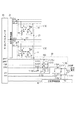
撮像装置は複数の画素10が複数行および複数列に配された画素アレイ1を有する。また、撮像装置は、画素10を行ごとに垂直走査する垂直走査回路20を有する。また、撮像装置は、各々が画素10の列に対応して設けられた複数の垂直信号線25を有する。また、撮像装置は複数の信号処理回路30を有する。複数の信号処理回路30の各々は、各列の垂直信号線25に対応して設けられているが、図1では、複数列の信号処理回路30を、一つのブロックの信号処理回路30として示している。また、撮像装置は水平走査回路40を有する。水平走査回路40は、各列の信号処理回路30を水平走査する。また、撮像装置は、垂直走査回路20と、信号処理回路30と、水平走査回路40の動作を制御するタイミングジェネレータ50を有する。また、撮像装置はアンプSAMPを有する。アンプSAMPは、各列の信号処理回路30が出力する信号を増幅した信号を、撮像装置の外部に出力する出力信号として、出力する。
The imaging apparatus has a pixel array 1 in which a plurality of
図2は、図1に示した撮像装置のうち、2行1列の画素10に関わる回路について示した図である。
FIG. 2 is a diagram showing a circuit related to the
画素10は、光電変換部PD、トランジスタTa、トランジスタTb、トランジスタTc、トランジスタSF、浮遊拡散容量FDを有する。光電変換部PDは入射光に基づく電荷を生成する。また、図1に示した画素アレイ1は、異なる行の画素10の浮遊拡散容量FD同士を電気的に接続するトランジスタTdを有する。トランジスタSFと、垂直信号線に電流を供給する不図示の電流源と、トランジスタSFの一方の主ノードに与えられる電源電圧VDDとによって、ソースフォロワ回路が構成される。画素10が有するトランジスタSFは、光電変換部PDの電荷に基づく信号を出力する増幅トランジスタである。
The
垂直走査回路20は、1行目の画素10が有するトランジスタTa、トランジスタTb、トランジスタTcにそれぞれ順に信号RESa、信号Txa、信号SELaを出力する。また、垂直走査回路20は、2行目の画素10が有するトランジスタTa、トランジスタTb、トランジスタTcにそれぞれ順に信号RESb、信号Txb、信号SELbを出力する。
The
信号処理回路30は、トランジスタTr100、トランジスタTr104、トランジスタTr105、トランジスタTr106、トランジスタTr107、容量素子C103、容量素子C104、差動増幅回路300を有する。差動増幅回路300は、容量素子C100、アンプAMP、トランジスタTr101、トランジスタTr102、トランジスタTr103、容量素子C101、容量素子C102を有する。容量素子C102の容量値は、容量素子C101の容量値よりも小さい。
The
水平走査回路40は、信号処理回路30のトランジスタTr106、トランジスタTr107に信号PHを出力する。また、信号処理回路30のその他のトランジスタTrには、タイミングジェネレータ50から、信号gain1、信号gain2、信号C0R、信号SW2、信号S11、信号N11が出力される。
The
また、本実施例の撮像装置は、撮像装置の外部に設けられた制御部によって、差動増幅回路300の増幅率が設定されている。具体的には、本実施例の撮像装置は、ISO感度が高い場合には、差動増幅回路300の増幅率を第1の増幅率とし、ISO感度が低い場合には、差動増幅回路300の増幅率を第1の増幅率よりも小さい第2の増幅率とする。
In the imaging apparatus of the present embodiment, the amplification factor of the
以下、撮像装置の第1の動作を中心に説明する。第1の動作は、画素10から垂直信号線25に出力された信号を、差動増幅回路300が、容量素子C100と容量素子C102を用いて第1の増幅率で増幅する際に行う動作である。後述する図4に示す撮像装置の第2の動作は、画素10から垂直信号線25に出力された信号を、差動増幅回路300が、容量素子C100と容量素子C101を用いて第1の増幅率よりも小さい第2の増幅率で増幅する際に行う動作である。
Hereinafter, the first operation of the imaging apparatus will be mainly described. The first operation is an operation performed when the
次に、図3を参照しながら、図2に示した撮像装置が行う第1の動作を中心に説明する。図3に示した各信号は、図2に示した各信号に対応している。以下に説明する第1の動作は、複数の画素10の各々の光電変換部PDが生成した電荷を、各々の浮遊拡散容量FDに転送する。そして、複数の画素10のトランジスタTcを同時にオンとして、該複数の画素10のトランジスタSFが出力する信号を垂直信号線25で混合する動作である。
Next, the first operation performed by the imaging apparatus shown in FIG. 2 will be mainly described with reference to FIG. Each signal shown in FIG. 3 corresponds to each signal shown in FIG. In the first operation described below, charges generated by the respective photoelectric conversion units PD of the plurality of
時刻t1よりも前の時刻において、垂直走査回路20と、水平走査回路40と、タイミングジェネレータ50は、図2に示した信号を全てLowレベル(以下、Lレベルと表記する)としている。
At a time before time t1, the
時刻t1に、タイミングジェネレータ50は、信号SW2をHレベルとする。これにより、垂直信号線15と、容量素子C100との間の電気的経路が導通する。
At time t1, the
時刻t2に、垂直走査回路20は、信号RESa、信号RESbをHighレベル(以下、Hレベルと表記する)とする。これにより、1行目の画素10の浮遊拡散容量FDと、2行目の画素10の浮遊拡散容量FDの電位がリセットされる。
At time t2, the
時刻t3に、垂直走査回路20は、信号Txaと信号TxbをそれぞれHレベルとする。これにより、1行目の画素10の光電変換部PDと、2行目の画素10の光電変換部PDの電荷がリセットされる。
At time t3, the
時刻t4に、垂直走査回路20は、信号Txaと信号TxbをそれぞれLレベルとする。
At time t4, the
時刻t5に、タイミングジェネレータ50は、信号C0RをHレベルとする。これにより、容量素子C100、容量素子C101、容量素子C102の電荷がリセットされる。また、時刻t5に、垂直走査回路20は、信号SELaと信号SELbをそれぞれHレベルとする。これにより、垂直信号線25の電位は、1行目の画素10のトランジスタSFが出力する信号と、2行目の画素10のトランジスタSFが出力する信号とを混合した信号の電位となる。この1行目の画素10のトランジスタSFが出力する信号と、2行目の画素10のトランジスタSFが出力する信号とを混合した信号をSFNMix信号と表記する。この1行目の画素10のトランジスタSFが出力する信号は、リセットされた浮遊拡散容量FDの電位に基づくノイズ信号である。また、この2行目の画素10のトランジスタSFが出力する信号は、リセットされた浮遊拡散容量FDの電位に基づくノイズ信号である。
At time t5, the
時刻t6に、タイミングジェネレータ50は、信号C0RをLレベルとする。これにより、容量素子C100は、SFNMix信号を保持する。また、時刻t6に、垂直走査回路20は、信号RESaと信号RESbをそれぞれLレベルとする。これにより、1行目の画素10の浮遊拡散容量FDと、2行目の画素10の浮遊拡散容量FDのリセットが解除される。
At time t6, the
時刻t7に、タイミングジェネレータ50は、信号gain1をHレベルとする。これにより、差動増幅回路300は、垂直信号線25から容量素子C100を介して入力される信号を第1の増幅率で増幅した信号を出力する。また、タイミングジェネレータ50は、信号N11をHレベルとする。これにより、差動増幅回路300と容量素子C104との間の電気的経路が導通する。その後、タイミングジェネレータ50は、信号N11をLレベルとする。これにより、容量素子C104は、差動増幅回路300が出力する信号を保持する。この容量素子C104が保持する信号は、差動増幅回路300のオフセット成分を主とするノイズ信号である。
At time t7, the
時刻t8に、垂直走査回路20は信号TXaと信号TXbとをそれぞれHレベルとする。これにより、1行目の画素10の光電変換部PDが生成した電荷が、該画素10の浮遊拡散容量FDに転送される。また、2行目の画素10の光電変換部PDが生成した電荷が、該画素10の浮遊拡散容量FDに転送される。その後、垂直走査回路20は、信号TXaと、信号TXbとをそれぞれLレベルとする。これにより、1行目の画素10のトランジスタSFは、1行目の画素10の光電変換部PDが生成した電荷に基づく信号を出力する。また、2行目の画素10のトランジスタSFは、2行目の画素10の光電変換部PDが生成した電荷に基づく信号を出力する。垂直信号線25の電位は、1行目の画素10のトランジスタSFが出力する信号と、2行目の画素10のトランジスタSFが出力する信号とを混合した信号の電位となる。1行目の画素10のトランジスタSFが出力する信号と、2行目の画素10のトランジスタSFが出力する信号とを混合した信号を、SFSMix信号と表記する。差動増幅回路300には、SFSMix信号から、容量素子C100が保持しているSFNMix信号を差し引いた信号が入力される。差動増幅回路300は、SFSMix信号を第1の増幅率で増幅した信号を出力する。
At time t8, the
時刻t9に、タイミングジェネレータ50は、信号S11をHレベルとする。これにより、容量素子C103と差動増幅回路300との間の電気的経路が導通する。その後、タイミングジェネレータ50は、信号S11をLレベルとする。これにより、容量素子C103は、差動増幅回路300が、第1の増幅率でSFSMix信号を増幅した信号を保持する。
At time t9, the
時刻t10に、タイミングジェネレータ50は、信号SW2をLレベルとする。これにより、画素10と容量素子C100との間の電気的経路が非導通となる。また、水平走査回路40は時刻t10に信号PHをHレベルとする。これにより、容量素子C103が保持した、第1の増幅率でSFSMix信号を増幅した信号と、容量素子C104が保持したノイズ信号とがそれぞれ、アンプSAMPに出力される。アンプSAMPは、第1の増幅率でSFSMix信号を増幅した信号とノイズ信号との差を増幅した信号を撮像装置の外部に出力する。
At time t10, the
次に、図4を参照しながら、図2に示した撮像装置が行う第2の動作を中心に説明する。図4に示した各信号は、図2に示した各信号に対応している。以下に説明する第2の動作は、複数の浮遊拡散容量FDを電気的に接続することによって、複数の光電変換部PDで生成した電荷同士を混合することで混合電荷を得る動作を含む。そして第2の動作は、画素10のトランジスタSFが、複数の浮遊拡散容量FDを電気的に接続することで得た混合電荷に基づく信号を垂直信号線25に出力する動作を含む。以下では、図3を参照しながら説明した第1の動作とは異なる点を中心に説明する。
Next, the second operation performed by the imaging apparatus shown in FIG. 2 will be mainly described with reference to FIG. Each signal shown in FIG. 4 corresponds to each signal shown in FIG. The second operation described below includes an operation of obtaining a mixed charge by electrically connecting a plurality of floating diffusion capacitors FD to mix charges generated by the plurality of photoelectric conversion units PD. The second operation includes an operation in which the transistor SF of the
図4に示した時刻t1の動作は、図3に示した時刻t1の動作と同じである。 The operation at time t1 shown in FIG. 4 is the same as the operation at time t1 shown in FIG.
時刻t2に、タイミングジェネレータ50は信号SW1をHレベルとする。これにより、図2に示した1行目の画素10の浮遊拡散容量FDと、2行目の画素10の浮遊拡散容量FDとが電気的に接続される。
At time t2, the
時刻t3から時刻t6までのそれぞれの動作は、図3に示した時刻t3から時刻t6までのそれぞれの動作と同じである。 Each operation from time t3 to time t6 is the same as each operation from time t3 to time t6 shown in FIG.
図3に示した時刻t7では、タイミングジェネレータ50は、信号gain1をHレベル、信号gain2をLレベルとしていた。一方、図4に示した時刻t7では、タイミングジェネレータ50は信号gain1をLレベル、信号gain2をHレベルとする。差動増幅回路300の増幅率は、容量素子C100の容量値/帰還容量の容量値として表される。上述したように、容量素子C102の容量値は、容量素子C101の容量値よりも小さい。従って、差動増幅回路300の増幅率は、図3で設定された第1の増幅率よりも小さい第2の増幅率に設定される。
At time t7 shown in FIG. 3, the
図4に示した時刻t7から時刻t8までのそれぞれの動作は、図3に示した時刻t7から時刻t8までのそれぞれの動作と同じである。時刻t8に、垂直走査回路20が信号TXa、信号TXbをそれぞれHレベルとすることにより、1行目および2行目の画素10の光電変換部PDが生成した電荷が、相互に電気的に接続された浮遊拡散容量FDにおいて混合される。1行目の画素10のトランジスタSFの、浮遊拡散容量FDに電気的に接続された入力ノードの電位と、2行目の画素10のトランジスタSFの、浮遊拡散容量FDに電気的に接続された入力ノードの電位は等しい。1行目のおよび2行目の画素10のトランジスタSFの各々は、トランジスタTcを介して垂直信号線25に、複数の浮遊拡散容量FDによって混合された電荷に基づく信号を出力する。この信号をFDMix信号と表記する。差動増幅回路300は、FDMix信号を第2の増幅率で増幅した信号を出力する。
Each operation from time t7 to time t8 shown in FIG. 4 is the same as each operation from time t7 to time t8 shown in FIG. At time t8, the
時刻t10に、タイミングジェネレータ50は、信号S11をHレベルとする。これにより、容量素子C103は、差動増幅回路300がFDMix信号を増幅した信号を保持する。
At time t10, the
時刻t11に、水平走査回路40は、信号PHをHレベルとする。これにより、容量素子C103が保持した、第2の増幅率でFDSMix信号を増幅した信号と、容量素子C104が保持したノイズ信号とがそれぞれ、アンプSAMPに出力される。アンプSAMPは、第1の増幅率でFDMix信号を増幅した信号とノイズ信号との差を増幅した信号を撮像装置の外部に出力する。このように第2の動作は、撮像装置が出力する、入射光を光電変換した電荷に基づく信号を、複数の画素10の全画素数よりも少なくして出力する動作である。
At time t11, the
このように、本実施例の撮像装置は差動増幅回路300の増幅率が第1の増幅率に場合には第1の動作を行う。そして、差動増幅回路300の増幅率が、第1の増幅率よりも小さい第2の増幅率の場合には、本実施例の撮像装置は第2の動作を行う。
As described above, the imaging apparatus according to the present embodiment performs the first operation when the amplification factor of the
第1の動作において、1行目の画素10のトランジスタSFが出力する信号と、2行目の画素10のトランジスタSFが出力する信号との信号振幅の差が大きくなるにつれ、信号振幅の小さいトランジスタSFには垂直信号線25からの電流が流れにくくなる。そして、1行目の画素10のトランジスタSFが出力する信号と、2行目の画素10のトランジスタSFが出力する信号との信号振幅の差が所定の値よりも大きくなると、信号振幅の大きいトランジスタSFには電流が流れなくなり、ソースフォロワ動作を停止する。よって、1行目と2行目の画素10の出力する信号を精度よく混合することができなくなる。従って、撮像装置が出力する信号を用いて、撮像装置の外部で生成する画像の画質が低下する。このような、1行目の画素10のトランジスタSFが出力する信号と、2行目の画素10のトランジスタSFが出力する信号との信号振幅の差が所定の値よりも大きくなるのは、撮像装置のISO感度が低い場合に顕著である。なぜなら、撮像装置のISO感度を低く設定した場合は、ISO感度を高く設定した場合に比して、高輝度の被写体から光が入射した画素10のトランジスタSFが出力する信号の信号振幅が大きくなるためである。従って、差動増幅回路300の増幅率が第2の増幅率の場合には、撮像装置は第1の動作を行わず、第2の動作を行う。
In the first operation, as the difference in signal amplitude between the signal output from the transistor SF of the
一方、第2の動作では、トランジスタSFが出力する信号のSN比が、第1の動作で垂直信号線25に表れる信号のSN比よりも低くなる傾向がある。なぜなら、トランジスタSFが出力する信号の電圧をV、浮遊拡散容量FDの容量値をC、光電変換部PDが蓄積した電荷をQとすると、V=Q/Cの関係が成り立つ。複数の浮遊拡散容量FDを電気的に接続することで、Cの値が増加する。従って、Qが一定とすると、Vの値は浮遊拡散容量FDの容量値が大きくなるにつれて小さくなる。本実施例においては、第1の動作に対し、第2の動作における浮遊拡散容量FDの容量値が大きいため、Qが一定であるとすると、第1の動作に対し、第2の動作はトランジスタSFが出力する信号の信号振幅が小さくなる。一方で、トランジスタSFが出力するノイズ信号は、トランジスタSFのノイズ成分が主である。従って、第1の動作と第2の動作とでトランジスタSFが出力するノイズ信号の信号値は同じと見なせる。よって、第2の動作の方が、第1の動作に対し、垂直信号線25に出力される信号のSN比が低くなる傾向がある。
On the other hand, in the second operation, the SN ratio of the signal output from the transistor SF tends to be lower than the SN ratio of the signal appearing on the
従って、ISO感度が高い場合、例えば夜間の撮影など撮影シーンの光量が小さい場合、第1の動作の方が第2の動作に比して、画素10がノイズ成分の少ない信号を出力できる。よって、ISO感度が高い場合、つまり差動増幅回路300の増幅率が第1の増幅率の場合には、第2の動作を行わず、第1の動作を行う。
Therefore, when the ISO sensitivity is high, for example, when the amount of light in a shooting scene such as nighttime shooting is small, the first operation can output a signal with less noise components than the second operation. Therefore, when the ISO sensitivity is high, that is, when the amplification factor of the
このように、差動増幅回路300の増幅率が大きい場合には、第1の動作を行い、差動増幅回路300の増幅率が小さい場合には第2の動作を行う。これにより、様々な撮影シーンにおいても、良好な画像を得るための信号を、撮像装置が出力することができる。
As described above, when the amplification factor of the
以下、第2の動作を行わずに第1の動作を行うための好適な条件に付いて説明する。画素10のトランジスタSFの入力ノードの電位の取り得る振幅の範囲の上限と下限との差をΔVFD(V)と表記する。このΔVFDは、撮像装置の信号処理回路30の増幅率によって変動する値である。
Hereinafter, preferable conditions for performing the first operation without performing the second operation will be described. The difference between the upper limit and the lower limit of the amplitude range that can be taken by the potential of the input node of the transistor SF of the
以下、信号処理回路30の増幅率の一例である差動増幅回路300の増幅率が変化する場合を例にΔVFDについて説明する。差動増幅回路300が出力する信号の取り得る振幅の範囲は、差動増幅回路300の増幅率が変化しても略一定である。よって、差動増幅回路300の増幅率が大きくなるに従って、差動増幅回路300に入力される信号の取り得る振幅の範囲が小さくなる。つまり、差動増幅回路300の増幅率が大きくなるに従って、画素10のトランジスタSFが出力する信号の取り得る振幅の範囲は小さくなる。トランジスタSFの出力する信号の振幅の範囲は、浮遊拡散容量FDの電位の取り得る範囲であるΔVFDに比例している。よって、差動増幅回路300の増幅率が大きくなるに従って、ΔVFDの値は小さくなる。つまり、高輝度の光が入射する画素10の浮遊拡散領域FDの電位と低輝度の浮遊拡散領域FDの電位との差は、差動増幅回路300の増幅率が大きくなるに従って小さくなる。
Hereinafter, ΔVFD will be described by taking as an example a case where the gain of the
垂直信号線25に不図示の電流源が供給する電流の値をI(μA)と表記する。また、1行目の画素10のトランジスタSFと2行目の画素10のトランジスタSFのチャネル幅をW、チャネル長をLと表記する。ここでは、1行目の画素10のトランジスタSFのW/Lと、2行目の画素10のトランジスタSFのW/Lは等しいとする。評価指数Zは以下の(1)式によって与えられる。
Z=I/{(W/L)×ΔVFD2} ・・・(1)
A value of a current supplied from a current source (not shown) to the
Z = I / {(W / L) × ΔVFD 2 } (1)
差動増幅回路300の増幅率が大きくなるにつれて、ΔVFDが小さくなることから、評価指数Zの値は大きくなる。評価指数Zが2.5以上となる場合の信号処理回路30の増幅率において、本実施例の撮像装置は、第2の動作を行わずに第1の動作を行うのが好ましい。本実施例の撮像装置は、信号処理回路30が第1の増幅率で信号を増幅する場合、評価指数Zの値は2.5以上である。
As the amplification factor of the
尚、本実施例では、第2の動作において、1行目および2行目の画素10のトランジスタTcを共にオンとしたが、一方のトランジスタTcのみをオンとするようにしてもよい。ただし、1行目および2行目の画素10のトランジスタTcを共にオンとする場合には、トランジスタSFのチャネル幅およびチャネル長をそれぞれ実効的に大きくすることができる。よって、1行目と2行目のトランジスタTcのいずれかをオンとする場合に比して、両方のトランジスタTcをオンとする場合は、SFMix信号に含まれる1/fノイズを低減できる効果を有している。
In the present embodiment, in the second operation, the transistors Tc of the
尚、本実施例では、画素10がトランジスタTcを有する例を説明した。他の例として、画素10がトランジスタTcを有さず、トランジスタSFが垂直信号線25に電気的に接続されていても良い。この場合、トランジスタTaの主ノードには、電圧VDD1と、電圧VDD1とは異なる電圧VDD2とが選択的に供給されるようにする。そして、垂直信号線25に信号を出力する行の画素10は、電圧VDD1によってトランジスタSFの入力ノードがリセットされることで、トランジスタSFがソースフォロワ動作を行うようにする。一方、他の非選択の行の画素10のトランジスタSFの入力ノードは電源電圧VDD2によってリセットされることで、トランジスタSFがオフ状態となる。撮像装置が第1の動作を行う場合には、複数行の画素10のトランジスタSFの入力ノードを、電圧VDD1によってリセットするようにすればよい。
In this embodiment, the example in which the
(実施例2)
以下、本実施例に関わる撮像装置について、実施例1と異なる点を中心に説明する。本実施例の第1の動作は、実施例1の第1の動作と同じである。本実施例の第2の動作が、実施例1の第2の動作と異なる。
(Example 2)
Hereinafter, the imaging apparatus according to the present embodiment will be described focusing on differences from the first embodiment. The first operation of the present embodiment is the same as the first operation of the first embodiment. The second operation of this embodiment is different from the second operation of the first embodiment.
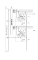
図5は、本実施例の撮像装置の構成を示した図である。図5では、図2に示した部材と同じ機能を有する部材については、図2で付した符号と同じ符号を付して表している。図5で示した撮像装置は、4行の画素10を示している。実施例1の図2に示した撮像装置は、複数の画素10の浮遊拡散容量FDを電気的に接続するトランジスタTdを有していたが、本実施例の撮像装置ではトランジスタTdを設けていない。
FIG. 5 is a diagram illustrating the configuration of the imaging apparatus according to the present embodiment. In FIG. 5, members having the same functions as those shown in FIG. 2 are denoted by the same reference numerals as those shown in FIG. The imaging device shown in FIG. 5 shows four rows of
本実施例の撮像装置は実施例1と同じく、差動増幅回路300の増幅率が第1の増幅率の場合には第1の動作を行い、差動増幅回路300の増幅率が第1の増幅率よりも小さい第2の増幅率の場合には第2の動作を行う。図5に示した撮像装置の、1行目と2行目の画素10に関わる第1の動作は、実施例1の撮像装置の第1の動作と同じである。また、3行目と4行目の画素10に関わる第1の動作についても、実施例1の1行目と2行目の画素10に関わる第1の動作と同じである。
As in the first embodiment, the imaging apparatus of the present embodiment performs the first operation when the amplification factor of the
次に、本実施例の撮像装置の第2の動作について説明する。本実施例の第2の動作は、一部の行の画素10から信号を出力させ、他の行の画素10から信号を出力させない間引き動作である。つまり、1行目と3行目の画素10のそれぞれから信号を順次出力させ、2行目と4行目の画素10からは信号を出力させない。これにより、1フレーム期間において撮像装置の第2の動作は、1行目と3行目の画素10に基づく信号を出力し、2行目と4行目の画素10に基づく信号を出力しない。
Next, the second operation of the image pickup apparatus of the present embodiment will be described. The second operation of this embodiment is a thinning operation in which signals are output from the
差動増幅回路300が第2の増幅率で信号を増幅する場合に第1の動作を行うと実施例1でも述べた様に次の課題が生じる。この課題とは、高輝度の光が入射した画素10と低輝度の光が入射した画素10との各々が出力する信号の差が所定の値よりも大きくなると、該画素10同士の信号を精度よく混合することができなくなることである。一方で、輝度の差が小さい画素同士では、該画素10同士の信号を精度よく混合することができる。よって、撮像装置が出力する信号によって生成する1枚の画像において、複数の画素10同士の信号を精度よく混合した領域と、精度よく混合することができなかった領域とが存在するため、画質が低下する。一方、本実施例の撮像装置は、第2の動作を行うことで、画像の全体に渡って、一部の画素10の信号を用いたものとすることができる。よって、画質の低下を避けることができる。
When the first operation is performed when the
一方で、差動増幅回路300が第1の増幅率で信号を増幅する場合には、本実施例の撮像装置においても実施例1と同様に、第1の動作を行う。これにより、実施例1で述べた効果と同じ効果を得ることができる。
On the other hand, when the
尚、本実施例では第2の動作において、垂直走査回路20が一部の行の画素10を選択する動作によって、複数の画素10の画素数よりも少ない数の信号を撮像装置が出力する例を説明した。他の例として、水平走査回路40が、全ての列の信号処理回路30のうちの一部の信号処理回路30のみからアンプSAMPに信号を出力させるようにしても良い。また第2の動作は、垂直走査回路20による一部の行のみの選択動作と、水平走査回路40による一部の列のみの信号処理回路30の選択動作とを組み合わせるようにしても良い。
In this embodiment, in the second operation, an example in which the imaging device outputs a smaller number of signals than the number of pixels of the plurality of
(実施例3)
本実施例の撮像装置について、実施例1と異なる点を中心に説明する。
(Example 3)
The imaging apparatus of the present embodiment will be described focusing on differences from the first embodiment.
図6は、本実施例の撮像装置の構成を示した図である。図6では、図2に示した部材と同じ機能を有する部材については、図2で付した符号と同じ符号を付して表している。実施例1の図2に示した撮像装置は、複数の画素10の浮遊拡散容量FDを電気的に接続するトランジスタTdを有していたが、本実施例の撮像装置ではトランジスタTdを設けていない。
FIG. 6 is a diagram illustrating the configuration of the imaging apparatus according to the present embodiment. In FIG. 6, members having the same functions as those shown in FIG. 2 are denoted by the same reference numerals as those shown in FIG. The image pickup apparatus shown in FIG. 2 according to the first embodiment includes the transistor Td that electrically connects the floating diffusion capacitors FD of the plurality of
また、本実施例の信号処理回路30は、容量素子C103、容量素子C106、トランジスタTr108、トランジスタTr109、トランジスタTr110、トランジスタTr111をさらに有する。トランジスタTr108、トランジスタTr109、トランジスタTr110、トランジスタTr111は順に、それぞれタイミングジェネレータ50から出力される信号S12、信号N12、信号SW3、信号SW4によって制御される。
Further, the
本実施例においても、差動増幅回路300が第1の増幅率の場合には撮像装置は第1の動作を行う。そして、差動増幅回路300が第1の増幅率よりも小さい第2の増幅率の場合には、撮像装置は第2の動作を行う。
Also in this embodiment, when the
本実施例の撮像装置の第1の動作では、信号S12、信号N12、信号SW3、信号SW4は常にLレベルである。他の信号の動作は、実施例1の第1の動作と同じである。 In the first operation of the imaging apparatus according to the present embodiment, the signal S12, the signal N12, the signal SW3, and the signal SW4 are always at the L level. The operation of other signals is the same as the first operation of the first embodiment.
本実施例の撮像装置の第2の動作について説明する。 A second operation of the imaging apparatus according to the present embodiment will be described.
図7は、図6に示した撮像装置の動作を示した図である。 FIG. 7 is a diagram illustrating the operation of the imaging apparatus illustrated in FIG.
時刻t1において、タイミングジェネレータ50は信号S12、信号N12、信号SW3、信号SW4の全てをLレベルとしている。また、時刻t1に、タイミングジェネレータ50は信号SW2をHレベルとする。これにより、画素10と差動増幅回路300との間の電気的経路が導通する。
At time t1, the
時刻t2に、垂直走査回路20は、信号RESaをHレベルとする。これにより、1行目の画素10の浮遊拡散容量FDの電位がリセットされる。
At time t2, the
時刻t3に、垂直走査回路20は、信号TXaをHレベルとする。これにより、1行目の画素10の光電変換部PDの電荷がリセットされる。その後、垂直走査回路20は時刻t4に信号TXaをLレベルとする。
At time t3, the
時刻t5に、タイミングジェネレータ50は、信号C0RをHレベルとする。これにより、差動増幅回路300の容量素子C100、容量素子C101、容量素子C102の電荷がリセットされる。また、時刻t5に、垂直走査回路20は、信号SELaをHレベルとする。これにより、1行目の画素10のトランジスタSFがトランジスタTcを介して垂直信号線25に信号を出力する。
At time t5, the
時刻t6に、垂直走査回路20は、信号RESaをLレベルとする。これにより、1行目の画素10の浮遊拡散容量FDのリセットが解除される。また、時刻t6に、タイミングジェネレータ50は信号C0RをLレベルとする。
At time t6, the
時刻t7に、タイミングジェネレータ50は信号N11をHレベルとする。これにより、トランジスタTr105がオンとなる。その後、タイミングジェネレータ50は信号N11をLレベルとする。これにより、容量素子C104は、差動増幅回路300が出力する信号を保持する。この容量素子C104が保持する信号は、差動増幅回路300のオフセット成分を主とするノイズ信号である。
At time t7, the
時刻t8に、垂直走査回路20は、信号TXaをHレベルとする。その後、垂直走査回路20は信号TXaをLレベルとする。これにより、1行目の画素10の光電変換部PDが生成した電荷が、浮遊拡散容量FDに転送される。1行目の画素10のトランジスタSFはトランジスタTcを介して垂直信号線25に、浮遊拡散容量FDが保持した電荷に基づく信号を出力する。この信号をFDS信号と表記する。差動増幅回路300は、FDS信号を第2の増幅率で増幅した信号を出力する。
At time t8, the
時刻t9に、タイミングジェネレータ50は、信号S11をHレベルとする。これにより、容量素子C103と差動増幅回路300との間の電気的経路が導通する。その後、タイミングジェネレータ50は、信号S11をLレベルとする。これにより、容量素子C103は、差動増幅回路300が、第2の増幅率でFDS信号を増幅した信号を保持する。
At time t9, the
その後、タイミングジェネレータ50と垂直走査回路20は、2行目の画素10のFDS信号と、差動増幅回路300のオフセット成分を主とするノイズ信号に関わる動作を行う。この動作は、容量素子C105がFDS信号を保持し、容量素子C106が差動増幅回路300のオフセット成分を主とするノイズ信号を保持する点を除いて、これまで述べた1行目の画素10に関わる動作と同じである。
Thereafter, the
時刻t10に、タイミングジェネレータ50は、信号SW3をHレベルとする。これにより、トランジスタTr110がオンとなり、容量素子C103が保持していた1行目の画素10のFDS信号と、容量素子C105が保持していた2行目の画素10のFDS信号とが混合される。また、同時刻に、タイミングジェネレータ50は、信号SW4をHレベルとする。これにより、トランジスタTr111がオンとなり、容量素子C104が保持していたノイズ信号と、容量素子C106が保持していたノイズ信号とが混合される。
At time t10, the
時刻t11に、水平走査回路40は、信号PHをHレベルとする。これにより1行目の画素10と2行目の画素10との混合されたFDS信号と、同じく混合されたノイズ信号とが、それぞれアンプSAMPに出力される。
At time t11, the
本実施例の第1の動作は、実施例1の第1の動作と同じである。つまり、第1の動作は、第1の光電変換部PDが生成した電荷に基づいてトランジスタSFが出力する信号と、第2の光電変換部PDが生成した電荷に基づいてトランジスタSFが出力する信号とを垂直信号線25で混合する動作である。本実施例の第2の動作は、第1の光電変換部PDが生成した電荷に基づく信号を、信号処理回路30が有する第1の容量素子である容量素子C103が保持する。また、第2の光電変換部PDが生成した電荷に基づく信号を信号処理回路30が有する、第2の容量素子である容量素子C105が保持する。この第1の容量素子と第2の容量素子とのそれぞれが保持した信号を混合する動作が、本実施例の第2の動作である。
The first operation of the present embodiment is the same as the first operation of the first embodiment. In other words, the first operation includes a signal output from the transistor SF based on the charge generated by the first photoelectric conversion unit PD and a signal output from the transistor SF based on the charge generated by the second photoelectric conversion unit PD. Are mixed by the
本実施例では、差動増幅回路300の増幅率が第1の増幅率の場合には、第2の動作を行わず、第1の動作を行う。また、差動増幅回路300の増幅率が第1の増幅率よりも小さい第2の増幅率の場合には、撮像装置は第1の動作を行わず、第2の動作を行う。
In the present embodiment, when the amplification factor of the
これにより、本実施例の撮像装置においても、実施例1で述べた効果と同じ効果を得ることができる。 Thereby, also in the imaging apparatus of a present Example, the same effect as the effect described in Example 1 can be acquired.
(実施例4)
本実施例の撮像装置について、実施例1と異なる点を中心に説明する。本実施例の撮像装置は、第2の動作が、1行目の画素10が出力する信号に基づくデジタル信号と、2行目の画素10が出力する信号に基づくデジタル信号とを混合する動作である点が、実施例1と異なる。
(Example 4)
The imaging apparatus of the present embodiment will be described focusing on differences from the first embodiment. In the imaging apparatus of the present embodiment, the second operation is an operation of mixing a digital signal based on a signal output from the
図8は、本実施例の撮像装置の構成を示した図である。図8では、図1に示した部材と同じ機能を有する部材については、図1で付した符号と同じ符号を付して表している。本実施例の撮像装置は、信号処理回路30が出力する信号をデジタル信号に変換するAD変換部60と、AD変換部60が出力するデジタル信号を保持するメモリ70とを有する。さらに、本実施例の撮像装置は、メモリ70が出力するデジタル信号を処理するデジタル信号処理部80と、デジタル信号処理部80からデジタル信号を出力させる水平走査回路90とを有する。信号処理回路30の構成は、図2に示した構成に対し、トランジスタTr104、トランジスタTr105、容量素子C103、容量素子C104、トランジスタTr106、トランジスタTr107を省略した構成とする。つまり、差動増幅回路300の出力ノードが、AD変換部60の入力ノードに電気的に接続された構成である。
FIG. 8 is a diagram illustrating the configuration of the imaging apparatus according to the present embodiment. 8, members having the same functions as those shown in FIG. 1 are denoted by the same reference numerals as those shown in FIG. The imaging apparatus according to the present exemplary embodiment includes an
メモリ70、デジタル信号処理部80は、各列の信号処理回路30に対応して、それぞれ各列に設けられている。
The
画素10の構成は、図6に示した構成と同じとする。
The configuration of the
本実施例においても、差動増幅回路300の増幅率が第1の増幅率の場合には、実施例1と同じく、第1の動作を行う。これにより、SFMix信号を第1の増幅率で差動増幅回路300が増幅した信号が、AD変換部60に出力される。AD変換部60は、この差動増幅回路300が出力する信号をデジタル信号に変換する。このデジタル信号をデジタルSFMix信号と表記する。そして、メモリ70は、AD変換部60から出力されるデジタルSFMix信号を保持する。デジタル信号処理部80は、メモリ70から出力されるデジタルSFMix信号を保持する。そして、水平走査回路90は、各列のデジタル信号処理部80から、それぞれのデジタル信号処理部80が保持したデジタルSFMix信号を出力させる。
Also in this embodiment, when the amplification factor of the
一方、差動増幅回路300の増幅率が第1の増幅率よりも小さい第2の増幅率の場合には、第2の動作を行う。本実施例の第2の動作について説明する。1行目の画素10が、当該画素10が有する光電変換部PDが生成した電荷に基づいて出力する信号を、信号処理回路30は第2の増幅率で増幅してAD変換部60に出力する。以下、この差動増幅回路300が出力した信号を増幅SF1信号と表記する。さらに、2行目の画素10が、当該画素10が有する光電変換部PDが生成した電荷に基づいて出力する信号を、信号処理回路30が第2の増幅率で増幅してAD変換部60に出力する。以下、この差動増幅回路300が出力した信号を増幅SF2信号と表記する。AD変換部60は、この増幅SF1信号と増幅SF2信号とをそれぞれデジタル信号に変換する。そして、メモリ70は、増幅SF1信号に基づくデジタル信号と、増幅SF2信号に基づくデジタル信号とをそれぞれ保持する。デジタル信号処理部80は、メモリ70が保持した増幅SF1信号に基づくデジタル信号と増幅SF2信号に基づくデジタル信号とをそれぞれ混合する。
On the other hand, when the amplification factor of the
水平走査回路90は、各列のデジタル信号処理部80が保持した、混合済みのデジタル信号を順次、各列のデジタル信号処理部80から出力させる。
The
これにより、本実施例の撮像装置においても、実施例1と同様の効果を得ることができる。 Thereby, also in the imaging apparatus of a present Example, the effect similar to Example 1 can be acquired.
尚、第1の動作、第2の動作のそれぞれ、あるいはいずれか一方の動作において、AD変換部60が、ノイズ信号をデジタル信号に変換する動作をさらに行っても良い。この場合、デジタル信号処理部80が、光電変換部PDが生成した電荷に基づくデジタル信号からノイズ信号に基づくデジタル信号を差し引く動作を行っても良い。
In each of the first operation, the second operation, or any one of the operations, the
尚、AD変換部60のAD変換形式は、時間に依存して電位が変化する参照信号とアナログ信号との比較を開始してから、比較の結果が変化するまでの時間を計測するスロープ型を用いることができる。また、AD変換部60のAD変換形式は、逐次比較型、フラッシュ型、パイプライン型、デルタシグマ型、二重積分型など、種々の形式とすることができる。
The AD conversion format of the
(実施例5)
本実施例の撮像装置について、実施例1と異なる点を中心に説明する。本実施例の撮像装置は、画素10の構成が実施例1とは異なる。
(Example 5)
The imaging apparatus of the present embodiment will be described focusing on differences from the first embodiment. The imaging apparatus of the present embodiment is different from the first embodiment in the configuration of the
図9は、本実施例の撮像装置の画素10と、垂直走査回路20と、タイミングジェネレータ50とを示した図である。図9では、図2に示した部材と同じ機能を有する部材については、図2で付した符号と同じ符号を付して表している。本実施例の撮像装置は、画素10が、トランジスタTe、容量素子Cadを有する点が、実施例1の撮像装置とは異なる。1行目および2行目の画素10のそれぞれのトランジスタTeは、タイミングジェネレータ50から出力される信号Ad1、信号Ad2のそれぞれによって制御される。本実施例の信号処理回路30の構成は、実施例1の信号処理回路30と同じである。
FIG. 9 is a diagram illustrating the
本実施例の第1の動作は、実施例1と同じとすることができる。信号Ad1、信号Ad2は、第1の動作の期間、Lレベルのままとする。 The first operation of this embodiment can be the same as that of the first embodiment. The signals Ad1 and Ad2 remain at the L level during the first operation.
次に、本実施例の第2の動作について説明する。図10は、本実施例の撮像装置の第2の動作を示した図である。本実施例の撮像装置の第2の動作は、信号Ad1、信号Ad2に関わる動作を除いて、実施例1と同じである。本実施例の撮像装置では、信号Txaと信号TxbとのそれぞれがHレベルとなってから、信号SELaと信号SELbとがそれぞれLレベルとなるまでの期間、タイミングジェネレータ50が信号Ad1と信号Ad2とをそれぞれHレベルとする。これにより、1行目の画素10の光電変換部PDが生成した電荷が、容量素子Cadと浮遊拡散容量FDとの合成容量に転送される。これにより、信号Ad1がLレベルの場合に比して、トランジスタSFが出力する信号振幅が小さくなる。2行目の画素10のトランジスタSFについても、1行目の画素10のトランジスタSFと同じく、信号Ad2がLレベルである場合に比して、出力する信号の信号振幅が小さくなる。従って、1行目の画素10のトランジスタSFが出力する信号と、2行目の画素10のトランジスタSFが出力する信号との差が、信号Ad1、信号Ad2が共にLレベルである場合に比して、相対的に小さくなる。これにより、実施例1の撮像装置に比して、1行目と2行目の画素10のそれぞれのトランジスタSFの出力する信号の差が大きいことによって生じる、一方のトランジスタSFのソースフォロワ動作の停止が起こりにくくなる。よって、実施例1の撮像装置に比して、さらに1行目の画素10と2行目の画素10のトランジスタSFのそれぞれが出力する信号の、混合を行いやすくすることができる。
Next, the second operation of this embodiment will be described. FIG. 10 is a diagram illustrating a second operation of the imaging apparatus according to the present embodiment. The second operation of the image pickup apparatus according to the present embodiment is the same as that of the first embodiment except for the operations related to the signal Ad1 and the signal Ad2. In the imaging apparatus according to the present embodiment, the
また、本実施例においても、実施例1で述べた様に、評価指数Zを用いて第1の動作と第2の動作のどちらを行うかを判断するようにしても良い。この場合には、評価指数Zが2.5以上となるような、信号処理回路30の増幅率の場合に、第1の動作を行うようにすればよい。
Also in the present embodiment, as described in the first embodiment, it may be determined using the evaluation index Z whether the first operation or the second operation is performed. In this case, the first operation may be performed when the amplification factor of the
(実施例6)
本実施例の撮像装置について、実施例4と異なる点を中心に説明する。
(Example 6)
The imaging apparatus of the present embodiment will be described focusing on differences from the fourth embodiment.
図11は、本実施例の撮像装置の構成を示した図である。図11では、図8に示した部材と同じ機能を有する部材については、図8で付した符号と同じ符号を付して表している。実施例4の撮像装置とは、信号処理回路35の構成が異なる。信号処理回路35は比較部41と、メモリ75と、参照信号供給部45と、カウンタ46とを有する。比較部41およびメモリ75のそれぞれは、各列の画素10に対応して設けられている。参照信号供給部45は、各列の比較部41に、時間に依存して電位が変化する参照信号を供給する。比較部41は、垂直信号線25に出力された信号と、参照信号とを比較した結果を示す比較結果信号をメモリ75に出力する。カウンタ46はクロックを計数したカウント信号を各列のメモリ75に供給する。メモリ75は、比較結果信号の信号値に基づいて、カウント信号を保持する。デジタル信号処理部85は、メモリ75が保持したデジタル信号を処理する。デジタル信号処理部85は、各列のメモリ75に対応して設けられている。水平走査回路95は、デジタル信号処理部85が処理したデジタル信号を、順次各列のデジタル信号処理部85から出力させる。
FIG. 11 is a diagram illustrating the configuration of the imaging apparatus according to the present embodiment. In FIG. 11, members having the same functions as those shown in FIG. 8 are denoted by the same reference numerals as those shown in FIG. The configuration of the
図12(a)は、図11に示した撮像装置の動作を示した図である。図12(a)に示したRAMPは、参照信号供給部45が出力する参照信号を示している。参照信号RAMPは、時刻t6から時刻t7の期間と、時刻t9から時刻t10の期間とにおいて、時間に依存した電位の変化を示す。参照信号RAMPは、本実施例の第1の動作においては、実線で示した電位の変化を示す、本実施例の第2の動作においては、破線で示した電位の変化を示す。実線の参照信号RAMPの傾きは、破線の参照信号RAMPの傾きよりも小さい。従って、同じ信号値のアナログ信号を実線の参照信号RAMPと破線の参照信号RAMPとでデジタル信号に変換した場合、実線の参照信号RAMPによって生成するデジタル信号の信号値が大きくなる。つまり、AD変換の増幅率が、実線の参照信号RAMOPでAD変換を行う方が、破線の参照信号RAMPでAD変換を行うよりも大きい。本実施例の撮像装置は、第1のISO感度の場合には第1の動作を行い、第1のISO感度よりも低い第2のISO感度の場合には第2の動作を行う。 FIG. 12A is a diagram illustrating an operation of the imaging apparatus illustrated in FIG. RAMP shown in FIG. 12A indicates a reference signal output from the reference signal supply unit 45. The reference signal RAMP indicates a change in potential depending on time in the period from time t6 to time t7 and in the period from time t9 to time t10. The reference signal RAMP indicates a change in potential indicated by a solid line in the first operation of this embodiment, and indicates a change in potential indicated by a broken line in the second operation of this embodiment. The slope of the solid line reference signal RAMP is smaller than the slope of the broken line reference signal RAMP. Therefore, when an analog signal having the same signal value is converted into a digital signal by the solid reference signal RAMP and the broken reference signal RAMP, the signal value of the digital signal generated by the solid reference signal RAMP becomes large. That is, the AD conversion gain is larger when AD conversion is performed with the solid reference signal RAMOP than when AD conversion is performed with the broken reference signal RAMP. The image pickup apparatus according to the present embodiment performs the first operation in the case of the first ISO sensitivity, and performs the second operation in the case of the second ISO sensitivity lower than the first ISO sensitivity.
時刻t5から時刻t7までの期間、垂直信号線25には、1行目の画素10が出力するノイズ信号と、2行目の画素10とが出力するノイズ信号とを混合した信号が出力されている。この信号を混合ノイズ信号と表記する。信号処理回路35は、実線で示した参照信号RAMPを用いて、垂直信号線25に出力されている混合ノイズ信号をデジタル信号に変換する。メモリ75は、この混合ノイズ信号に基づくデジタル信号を保持する。
During the period from time t5 to time t7, a signal obtained by mixing the noise signal output from the
また、時刻t9から時刻t10の期間、垂直信号線25にはSFMix信号が出力されている。信号処理回路35は、実線で示した参照信号RAMPを用いて、垂直信号線25に出力されているSFMix信号をデジタル信号に変換する。メモリ75は、このSFMix信号に基づくデジタル信号を保持する。
In addition, the SFmix signal is output to the
デジタル信号処理部85は、SFMix信号に基づくデジタル信号と、混合ノイズ信号に基づくデジタル信号との差のデジタル信号を生成する。
The digital
図12(b)は、本実施例の第2の動作を示した図である。時刻t8から時刻t9の期間、1行目の画素10はノイズ信号を出力している。信号処理回路35は、該ノイズ信号を破線で示した参照信号RAMPを用いてデジタル信号に変換する。メモリ75は、ノイズ信号に基づくデジタル信号を保持する。このデジタル信号をデジタルN1信号と表記する。また、時刻t10から時刻t11の期間、1行目の画素10は、光電変換部PDが蓄積した電荷に基づく信号を出力している。信号処理回路35は、該信号を破線で示した参照信号RAMPを用いてデジタル信号に変換する。メモリ75は、1行目の画素10の光電変換部PDの電荷に基づくデジタル信号を保持する。このデジタル信号をデジタルS1信号と表記する。
FIG. 12B is a diagram showing a second operation of the present embodiment. During the period from time t8 to time t9, the
時刻t16から時刻t17の期間、2行目の画素10はノイズ信号を出力している。信号処理回路35は、該ノイズ信号を破線で示した参照信号RAMPを用いてデジタル信号に変換する。メモリ75は、ノイズ信号に基づくデジタル信号を保持する。このデジタル信号をデジタルN2信号と表記する。また、時刻t19から時刻t20の期間、2行目の画素10は、光電変換部PDが蓄積した電荷に基づく信号を出力している。信号処理回路35は、該信号を破線で示した参照信号RAMPを用いてデジタル信号に変換する。メモリ75は、2行目の画素10の光電変換部PDの電荷に基づくデジタル信号を保持する。このデジタル信号をデジタルS2信号と表記する。
During the period from time t16 to time t17, the
デジタル信号処理部85は、デジタルN1信号とデジタルN2信号とを混合する。また、デジタル信号処理部85は、デジタルS1信号とデジタルS2信号とを混合する。この混合の動作は、デジタル信号同士を加算する処理や、デジタル信号同士の平均を取得する処理とすることができる。
The digital
このように、AD変換の増幅率が大きい場合、すなわち参照信号RAMPの傾きが小さい場合には、本実施例の撮像装置は第1の動作を行う。また、AD変換の増幅率が小さい場合、すなわち参照信号RAMPの傾きが大きい場合には、本実施例の撮像装置は第2の動作を行う。これにより、本実施例の撮像装置においても、実施例1と同じ効果を得ることができる。 As described above, when the gain of AD conversion is large, that is, when the inclination of the reference signal RAMP is small, the imaging apparatus of the present embodiment performs the first operation. Further, when the AD conversion gain is small, that is, when the slope of the reference signal RAMP is large, the imaging apparatus of the present embodiment performs the second operation. Thereby, also in the imaging apparatus of a present Example, the same effect as Example 1 can be acquired.
尚、本実施例では、第2の動作としてデジタル信号処理部85が、複数行の画素10の各々の光電変換部PDが生成した電荷に基づくデジタル信号を混合する例を説明した。他の第2の動作の例として、実施例1で述べたように、複数行の画素10の浮遊拡散容量FDを用いて電荷を混合するようにしても良い。
In the present embodiment, the example in which the digital
また、他の第2の動作として、実施例2のように、一部の行の画素10から信号を出力させる動作としても良い。
Further, as another second operation, as in the second embodiment, an operation for outputting a signal from the
また、本実施例の撮像装置の画素10を、実施例5の画素10と同じ構成として、第1の動作において、光電変換部PDが生成した電荷を、容量素子Cadと浮遊拡散容量FDとに転送するようにしても良い。これにより、実施例5の撮像装置と同じ効果を得ることができる。
Further, the
(実施例7)
図13は、本実施例の撮像システムを示した図である。
(Example 7)
FIG. 13 is a diagram illustrating the imaging system of the present embodiment.
本実施例の撮像システムは、撮像装置101、撮像装置に光を導く光学系100、撮像装置101が出力する信号を増幅する増幅部102を有する。さらに撮像システムは、増幅部102が出力する信号をデジタル信号に変換するとともにデジタル信号を用いて画像を生成する出力信号処理部104を有する。さらに撮像システムは、出力信号処理部104が出力する画像を表示する表示部105と、出力信号処理部104が出力する画像を記録する記録部106とを有する。さらに、撮像システムは、撮像装置の動作を、第1の動作と第2の動作とを切り替えるモード切替部107と、増幅部102の増幅率を設定する増幅率設定部108を有する。さらに撮像システムは、撮像システムの全体を制御する全体制御部109を有する。撮像装置101と、増幅部102は、互いに異なる半導体基板上に設けられている。
The imaging system of the present embodiment includes an
本実施例の撮像装置101の構成は、実施例1〜6のいずれの構成でも適用できる。以下は、実施例1の撮像装置を適用した場合を例に説明する。
The configuration of the
全体制御部109は、増幅率設定部108に対し、増幅部102の増幅率を設定する制御信号を出力する。ここでは、全体制御部109が増幅率設定部108に対し、第1の増幅率と、第1の増幅率よりも小さい第2の増幅率とのいずれかを設定する制御信号を出力する例を説明する。そして、全体制御部109は、モード切替部107に対し、撮像装置101の動作モードを設定する制御信号を出力する。
The
全体制御部109が増幅率設定部108に対し、増幅部102の増幅率を第1の増幅率とする制御信号を出力する場合を説明する。増幅率設定部108は、この制御信号に基づいて、増幅部102に第1の増幅率を設定する。そして、全体制御部109は、モード切替部107に対し、撮像装置101を第1の動作とする制御信号を出力する。モード切替部107はこの制御信号に基づいて、撮像装置101の動作を第1の動作に設定する。
A case where the
一方、全体制御部109が増幅率設定部108に対し、増幅部102の増幅率を第2の増幅率とする制御信号を出力する場合を説明する。増幅率設定部108は、この制御信号に基づいて、増幅部102に第2の増幅率を設定する。そして、全体制御部109は、モード切替部107に対し、撮像装置101を第2の動作とする制御信号を出力する。モード切替部107はこの制御信号に基づいて、撮像装置101の動作を第2の動作に設定する。
On the other hand, a case where the
これにより、増幅部102の増幅率が第1の増幅率の場合には、撮像装置101は第1の動作を行う。また、増幅率の増幅率が第1の増幅率よりも小さい第2の増幅率の場合には、撮像装置101は第2の動作を行う。これにより、本実施例の撮像システムにおいても、実施例1の撮像装置が得た効果と同じ効果を得ることができる。
Thereby, when the amplification factor of the
尚、撮像装置101の内部に設けられた差動増幅回路300の増幅率は、増幅部102の増幅率に連動するようにしても良い。
Note that the amplification factor of the
また、本実施例では、出力信号処理部104が、AD変換機能を有する例を説明した。他の例として、増幅部102がAD変換機能を有するようにしても良い。この場合には、増幅率設定部108は、AD変換の増幅率を第1の増幅率と、第2の増幅率のいずれかを設定する。この場合においても、全体制御部109は、第1の増幅率の場合には、モード切替部107に対して、撮像装置101を第1の動作に設定する制御信号を出力する。同様に、全体制御部109は、第2の増幅率の場合には、モード切替部107に対して、撮像装置101を第2の動作に設定する制御信号を出力する。この例においても、実施例6と同じ効果を得ることができる。
In the present embodiment, the output
1 画素アレイ
10 画素
20 垂直走査回路
25 垂直信号線
30 信号処理回路
40 水平走査回路
50 タイミングジェネレータ
1
Claims (19)
前記複数の画素は、第1の画素と第2の画素とを有し、
前記第1の画素は、第1の光電変換部と、第1の増幅トランジスタとを有し、
前記第2の画素は、第2の光電変換部と、第2の増幅トランジスタとを有する撮像装置の駆動方法であって、
前記信号処理回路は前記信号線に出力された信号を、第1の増幅率と前記第1の増幅率よりも小さい第2の増幅率との一方で増幅し、
前記信号処理回路が、前記信号線に出力された信号を前記第1の増幅率で増幅する場合には、第1の動作を行い、
前記信号処理回路が、前記信号線に出力された信号を前記第2の増幅率で増幅する場合には前記第1の動作を行わずに第2の動作を行い、
前記第1の動作は、前記第1の増幅トランジスタが前記第1の光電変換部が生成した電荷に基づく第1の信号を前記信号線に出力する期間と、前記第2の増幅トランジスタが前記第2の光電変換部が生成した電荷に基づく第2の信号を前記信号線に出力する期間との少なくとも一部の期間を重ねることによって、前記第1の信号と前記第2の信号とを前記信号線において混合する動作であり、
前記第2の動作は、
前記撮像装置が、入射光を光電変換した電荷に基づく信号の数を、前記第1の光電変換部と前記第2の光電変換部とが出力する信号の数よりも少なくして出力する動作であることを特徴とする撮像装置の駆動方法。 It includes a plurality of pixels, and signal Route, and a signal processing circuit,
The plurality of pixels include a first pixel and a second pixel,
The first pixel includes a first photoelectric conversion unit and a first amplification transistor,
The second pixel is a driving method of an imaging device having a second photoelectric conversion unit and a second amplification transistor,
A signal the signal processing circuit is output to the signal Line, amplified in one of the first amplification factor and the first smaller than the amplification factor a second amplification factor,
Said signal processing circuit, when amplifying a signal output to the signal Line in the first amplification factor, performs a first operation,
The signal processing circuit performs the second operation without performing the first operation in the case of amplifying a signal output to the signal Line with the second amplification factor,
The first operation, a period for outputting a first signal based on the electric charges of the first amplifier transistor is generated by the first photoelectric conversion unit to the signal Line, said second amplifying transistor is the first by overlaying at least a portion of the period of the period in which the photoelectric conversion unit 2 outputs a second signal based on the electric charges generated in the signal Line, said signal and said first signal and said second signal The operation of mixing at the line,
The second operation is as follows.
In the operation in which the imaging device outputs the number of signals based on charges obtained by photoelectric conversion of incident light, less than the number of signals output by the first photoelectric conversion unit and the second photoelectric conversion unit. There is provided a driving method of an imaging apparatus.
前記第2の画素は電荷を保持する第2の浮遊拡散容量を有し、
前記第1の信号は、前記第1の光電変換部が生成した電荷を保持した前記第1の浮遊拡散容量の電位に基づいて前記第1の増幅トランジスタが出力する信号であり、
前記第2の信号は、前記第2の光電変換部が生成した電荷を保持した前記第2の浮遊拡散容量の電位に基づいて前記第2の増幅トランジスタが出力する信号であり、
前記混合された電荷は、前記第1の光電変換部が生成した電荷と前記第2の光電変換部が生成した電荷とをともに、前記第1の浮遊拡散容量と前記第2の浮遊拡散容量に保持されることによって生成する電荷であることを特徴とする請求項2に記載の撮像装置の駆動方法。 The first pixel has a first floating diffusion capacitor for holding charge;
The second pixel has a second floating diffusion capacitor for holding electric charge,
The first signal is a signal output from the first amplification transistor based on a potential of the first floating diffusion capacitor that holds the charge generated by the first photoelectric conversion unit,
The second signal is a signal output from the second amplification transistor based on the potential of the second floating diffusion capacitor that holds the charge generated by the second photoelectric conversion unit,
The mixed charge includes both the charge generated by the first photoelectric conversion unit and the charge generated by the second photoelectric conversion unit in the first floating diffusion capacitor and the second floating diffusion capacitor. 3. The method of driving an imaging apparatus according to claim 2, wherein the charge is generated by being held.
前記第1の信号に基づく信号と前記第2の信号に基づく信号とを混合する前記動作が、
前記第1の信号をAD変換したデジタル信号と、前記第2の信号をAD変換したデジタル信号とを混合することを特徴とする請求項5に記載の撮像装置の駆動方法。 The signal processing circuit includes an AD converter for AD converting the signal output to the signal Line into a digital signal,
The operation of mixing a signal based on the first signal and a signal based on the second signal comprises:
6. The method according to claim 5, wherein a digital signal obtained by AD converting the first signal and a digital signal obtained by AD converting the second signal are mixed.
前記複数の画素は、第1の画素と第2の画素とを有し、
前記第1の画素は、第1の光電変換部と、第1の容量素子と、第1の浮遊拡散容量と、第1の増幅トランジスタとを有し、
前記第2の画素は、第2の光電変換部と、第2の容量素子と、第2の浮遊拡散容量と、第2の増幅トランジスタとを有する撮像装置の駆動方法であって、
前記信号処理回路は前記信号線に出力された信号を、第1の増幅率と前記第1の増幅率よりも小さい第2の増幅率との一方で増幅し、
前記信号処理回路が、前記信号線に出力された信号を前記第1の増幅率で増幅する場合には、第1の動作を行い、
前記信号処理回路が、前記信号線に出力された信号を前記第2の増幅率で増幅する場合には前記第1の動作を行わずに第2の動作を行い、
前記第1の動作は、
前記第1の光電変換部が生成した電荷を前記第1の容量素子が保持せずに前記第1の浮遊拡散容量が保持し、
前記第2の光電変換部が生成した電荷を前記第2の容量素子が保持せずに前記第2の浮遊拡散容量が保持し、
前記第1の増幅トランジスタが前記第1の浮遊拡散容量の電位に基づく第1の信号を前記信号線に出力する期間と、前記第2の増幅トランジスタが前記第2の浮遊拡散容量の電位に基づく第2の信号を前記信号線に出力する期間との少なくとも一部の期間を重ねることによって、前記第1の信号と前記第2の信号とを前記信号線において混合する動作であり、
前記第2の動作は、
前記第1の光電変換部が生成した電荷を前記第1の容量素子と前記第1の浮遊拡散容量との第1の合成容量が保持し、
前記第2の光電変換部が生成した電荷を前記第2の容量素子と前記第2の浮遊拡散容量との第2の合成容量が保持し、
前記第1の増幅トランジスタが前記第1の浮遊拡散容量の電位に基づく第1の信号を前記信号線に出力する期間と、前記第2の増幅トランジスタが前記第2の浮遊拡散容量の電位に基づく第2の信号を前記信号線に出力する期間との少なくとも一部の期間を重ねることによって、前記第1の信号と前記第2の信号とを前記信号線において混合する動作であることを特徴とする撮像装置の駆動方法。 It includes a plurality of pixels, and signal Route, and a signal processing circuit,
The plurality of pixels include a first pixel and a second pixel,
The first pixel includes a first photoelectric conversion unit, a first capacitor, a first floating diffusion capacitor, and a first amplification transistor,
The second pixel is a driving method of an imaging apparatus including a second photoelectric conversion unit, a second capacitor, a second floating diffusion capacitor, and a second amplification transistor,
A signal the signal processing circuit is output to the signal Line, amplified in one of the first amplification factor and the first smaller than the amplification factor a second amplification factor,
Said signal processing circuit, when amplifying a signal output to the signal Line in the first amplification factor, performs a first operation,
The signal processing circuit performs the second operation without performing the first operation in the case of amplifying a signal output to the signal Line with the second amplification factor,
The first operation is:
The first floating diffusion capacitor holds the charge generated by the first photoelectric conversion unit without the first capacitor element holding the charge,
The second floating diffusion capacitor holds the charge generated by the second photoelectric conversion unit without the second capacitor element holding the charge,
A period in which the first amplification transistor outputs a first signal based on the potential of the first floating diffusion capacitance to the signal Line, said second amplifying transistor is based on the potential of the second floating diffusion capacitance by overlaying at least a portion of the period and the period for outputting the second signal to the signal Line is a first signal and said second signal an operation of mixing in the signal Line,
The second operation is as follows.
The first combined capacitor of the first capacitor element and the first floating diffusion capacitor holds the charge generated by the first photoelectric conversion unit,
The second combined capacitor of the second capacitor element and the second floating diffusion capacitor holds the charge generated by the second photoelectric conversion unit,
A period in which the first amplification transistor outputs a first signal based on the potential of the first floating diffusion capacitance to the signal Line, said second amplifying transistor is based on the potential of the second floating diffusion capacitance by overlaying at least a portion of the period and the period for outputting the second signal to the signal Line, and wherein the said first signal and said second signal said an operation to mix the signal Line Method of driving an imaging apparatus.
前記差動増幅回路が、前記第1の増幅率と前記第2の増幅率とで前記信号線に出力された信号を増幅することを特徴とする請求項1〜9のいずれか1項に記載の撮像装置の駆動方法。 The signal processing circuit includes a differential amplifier circuit;
It said differential amplifier circuit, according to any one of claims 1-9, characterized in that amplifies the first signal output to the signal Line amplification factor and said second amplification factor of Driving method of the imaging apparatus.
前記第1の増幅トランジスタと前記第2の増幅トランジスタの各々のチャネル幅をW、
前記信号線に供給される電流の値をI(μA)、
前記第1の増幅トランジスタの入力ノードの電位と前記第2の増幅トランジスタの入力ノードの電位が前記第1の増幅率において取り得る範囲の上限と下限との差をΔVFD(V)として、
以下の式で表される評価指数Zの値が2.5以上であることを特徴とする請求項1〜10のいずれか1項に記載の撮像装置の駆動方法。
Z=I/{(W/L)×ΔVFD2} The channel length of each of the first amplification transistor and the second amplification transistor is L,
The channel width of each of the first amplification transistor and the second amplification transistor is W,
I (.mu.A) the value of the current supplied to the signal Line,
The difference between the upper limit and the lower limit of the range that the potential of the input node of the first amplification transistor and the potential of the input node of the second amplification transistor can take in the first amplification factor is ΔVFD (V),
The method of driving an imaging apparatus according to claim 1, wherein a value of the evaluation index Z represented by the following expression is 2.5 or more.
Z = I / {(W / L) × ΔVFD 2 }
前記複数の画素は、第1の画素と第2の画素とを有し、
前記第1の画素は、第1の光電変換部と、第1の増幅トランジスタとを有し、
前記第2の画素は、第2の光電変換部と、第2の増幅トランジスタとを有する撮像装置と、前記撮像装置を制御する制御部とを有する撮像システムの駆動方法であって、
前記制御部が第1のISO感度を設定した場合には、前記撮像装置は第1の動作を行い、
前記制御部が第1のISO感度よりも低い第2のISO感度を設定した場合には、前記撮像装置は前記第1の動作を行わずに第2の動作を行い、
前記第1の動作は、前記第1の増幅トランジスタが前記第1の光電変換部が生成した電荷に基づく第1の信号を前記信号線に出力する期間と、前記第2の増幅トランジスタが前記第2の光電変換部が生成した電荷に基づく第2の信号を前記信号線に出力する期間との少なくとも一部の期間を重ねることによって、前記第1の信号と前記第2の信号とを前記信号線において混合する動作であり、
前記第2の動作は前記撮像装置が、入射光を光電変換した電荷に基づく信号を、前記第1の動作とは異なる方法によって、前記複数の画素の数よりも少なくして出力する動作であることを特徴とする撮像システムの駆動方法。 Includes a plurality of pixels, and a signal Line,
The plurality of pixels include a first pixel and a second pixel,
The first pixel includes a first photoelectric conversion unit and a first amplification transistor,
The second pixel is a driving method of an imaging system including an imaging device having a second photoelectric conversion unit, a second amplification transistor, and a control unit that controls the imaging device,
When the control unit sets the first ISO sensitivity, the imaging device performs a first operation,
When the control unit sets a second ISO sensitivity lower than the first ISO sensitivity, the imaging device performs a second operation without performing the first operation,
The first operation, a period for outputting a first signal based on the electric charges of the first amplifier transistor is generated by the first photoelectric conversion unit to the signal Line, said second amplifying transistor is the first by overlaying at least a portion of the period of the period in which the photoelectric conversion unit 2 outputs a second signal based on the electric charges generated in the signal Line, said signal and said first signal and said second signal The operation of mixing at the line,
The second operation is an operation in which the imaging device outputs a signal based on a charge obtained by photoelectrically converting incident light by using a method different from the first operation, less than the number of the plurality of pixels. An imaging system drive method characterized by the above.
前記第1の増幅トランジスタと前記第2の増幅トランジスタの各々のチャネル幅をW、
前記信号線に供給される電流の値をI(μA)、
前記第1の増幅トランジスタの入力ノードの電位と前記第2の増幅トランジスタの入力ノードの電位が前記第1のISO感度において取り得る範囲の上限と下限との差をΔVFD(V)として、
以下の式で表される評価指数Zの値が2.5以上であることを特徴とする請求項12に記載の撮像システムの駆動方法。
Z=I/{(W/L)×ΔVFD2} The channel length of each of the first amplification transistor and the second amplification transistor is L,
The channel width of each of the first amplification transistor and the second amplification transistor is W,
I (.mu.A) the value of the current supplied to the signal Line,
The difference between the upper limit and the lower limit of the range that the potential of the input node of the first amplification transistor and the potential of the input node of the second amplification transistor can take in the first ISO sensitivity is defined as ΔVFD (V).
The method of driving an imaging system according to claim 12, wherein the value of the evaluation index Z expressed by the following formula is 2.5 or more.
Z = I / {(W / L) × ΔVFD 2 }
前記複数の画素は、第1の画素と第2の画素とを有し、
前記第1の画素は、第1の光電変換部と、第1の増幅トランジスタとを有し、
前記第2の画素は、第2の光電変換部と、第2の増幅トランジスタとを有する撮像装置と、前記撮像装置とは別の半導体基板に設けられるとともに、前記撮像装置が出力する信号を増幅する増幅部とを有する撮像システムの駆動方法であって、
前記増幅部は前記撮像装置から出力された信号を、第1の増幅率と前記第1の増幅率よりも小さい第2の増幅率との一方で増幅し、
前記増幅部が、前記撮像装置から出力された信号を前記第1の増幅率で増幅する場合には、前記撮像装置は第1の動作を行い、
前記増幅部が、前記撮像装置から出力された信号を前記第2の増幅率で増幅する場合には、前記撮像装置は前記第1の動作を行わずに第2の動作を行い、
前記第1の動作は、前記第1の増幅トランジスタが前記第1の光電変換部が生成した電荷に基づく第1の信号を前記信号線に出力する期間と、前記第2の増幅トランジスタが前記第2の光電変換部が生成した電荷に基づく第2の信号を前記信号線に出力する期間との少なくとも一部の期間を重ねることによって、前記第1の信号と前記第2の信号とを前記信号線において混合する動作であり、
前記第2の動作は前記撮像装置が、入射光を光電変換した電荷に基づく信号を、前記第1の動作とは異なる方法によって、前記複数の画素の数よりも少なくして出力する動作であることを特徴とする撮像システムの駆動方法。 Includes a plurality of pixels, and a signal Line,
The plurality of pixels include a first pixel and a second pixel,
The first pixel includes a first photoelectric conversion unit and a first amplification transistor,
The second pixel is provided on an imaging device having a second photoelectric conversion unit and a second amplification transistor, and a semiconductor substrate different from the imaging device, and amplifies a signal output from the imaging device. A driving method of an imaging system having an amplification unit,
The amplifying unit amplifies the signal output from the imaging device with one of a first gain and a second gain smaller than the first gain,
When the amplifying unit amplifies the signal output from the imaging device with the first amplification factor, the imaging device performs a first operation,
When the amplification unit amplifies the signal output from the imaging device at the second amplification factor, the imaging device performs the second operation without performing the first operation,
The first operation, a period for outputting a first signal based on the electric charges of the first amplifier transistor is generated by the first photoelectric conversion unit to the signal Line, said second amplifying transistor is the first by overlaying at least a portion of the period of the period in which the photoelectric conversion unit 2 outputs a second signal based on the electric charges generated in the signal Line, said signal and said first signal and said second signal The operation of mixing at the line,
The second operation is an operation in which the imaging device outputs a signal based on a charge obtained by photoelectrically converting incident light by using a method different from the first operation, less than the number of the plurality of pixels. An imaging system drive method characterized by the above.
前記第1の増幅トランジスタの入力ノードの電位と前記第2の増幅トランジスタの入力ノードの電位が前記第1の増幅率において取り得る範囲の上限と下限との差をΔVFD(V)として、
以下の式で表される評価指数Zの値が2.5以上であることを特徴とする請求項14または15に記載の撮像システムの駆動方法。
Z=I/{(W/L)×ΔVFD2} The channel length of each of the first amplification transistor and the second amplification transistor is L, the channel width of each of the first amplification transistor and the second amplification transistor is W, and the current supplied to the signal line Value of I (μA),
The difference between the upper limit and the lower limit of the range that the potential of the input node of the first amplification transistor and the potential of the input node of the second amplification transistor can take in the first amplification factor is ΔVFD (V),
16. The method for driving an imaging system according to claim 14, wherein the value of the evaluation index Z expressed by the following formula is 2.5 or more.
Z = I / {(W / L) × ΔVFD2}
前記複数の画素は、第1の画素と第2の画素とを有し、The plurality of pixels include a first pixel and a second pixel,
前記第1の画素は、第1の光電変換部と、第1の増幅トランジスタとを有し、The first pixel includes a first photoelectric conversion unit and a first amplification transistor,
前記第2の画素は、第2の光電変換部と、第2の増幅トランジスタとを有し、The second pixel includes a second photoelectric conversion unit and a second amplification transistor,
前記信号処理回路は前記信号線に出力された信号を、第1の増幅率と前記第1の増幅率よりも小さい第2の増幅率との一方で増幅し、The signal processing circuit amplifies the signal output to the signal line with one of a first gain and a second gain smaller than the first gain,
前記信号処理回路が、前記信号線に出力された信号を前記第1の増幅率で増幅する場合には、前記制御部は、前記第1の画素と前記第2の画素とに第1の動作を行わせ、When the signal processing circuit amplifies the signal output to the signal line with the first amplification factor, the control unit performs a first operation on the first pixel and the second pixel. Let
前記信号処理回路が、前記信号線に出力された信号を前記第2の増幅率で増幅する場合には、前記制御部は、前記第1の画素と前記第2の画素とに対し、前記第1の動作を行わせずに第2の動作を行わせ、When the signal processing circuit amplifies the signal output to the signal line at the second amplification factor, the control unit performs the first operation on the first pixel and the second pixel. The second operation is performed without performing the first operation,
前記第1の動作は、前記第1の増幅トランジスタが前記第1の光電変換部が生成した電荷に基づく第1の信号を前記信号線に出力する期間と、前記第2の増幅トランジスタが前記第2の光電変換部が生成した電荷に基づく第2の信号を前記信号線に出力する期間との少なくとも一部の期間を重ねることによって、前記第1の信号と前記第2の信号とを前記信号線において混合する動作であり、The first operation includes a period in which the first amplification transistor outputs a first signal based on the charge generated by the first photoelectric conversion unit to the signal line, and the second amplification transistor performs the first operation. The second signal based on the charge generated by the two photoelectric conversion units is overlapped with at least a part of the period in which the second signal is output to the signal line, whereby the first signal and the second signal are converted into the signal. Mixing in the line,
前記第2の動作は、The second operation is as follows.
前記撮像装置が、入射光を光電変換した電荷に基づく信号の数を、前記第1の光電変換部と前記第2の光電変換部とが出力する信号の数よりも少なくして出力する動作であることを特徴とする撮像装置。In the operation in which the imaging device outputs the number of signals based on charges obtained by photoelectric conversion of incident light, less than the number of signals output by the first photoelectric conversion unit and the second photoelectric conversion unit. There is an imaging apparatus.
前記複数の画素は、第1の画素と第2の画素とを有し、The plurality of pixels include a first pixel and a second pixel,
前記第1の画素は、第1の光電変換部と、第1の増幅トランジスタとを有し、The first pixel includes a first photoelectric conversion unit and a first amplification transistor,
前記第2の画素は、第2の光電変換部と、第2の増幅トランジスタとを有し、The second pixel includes a second photoelectric conversion unit and a second amplification transistor,
前記信号処理回路は前記信号線に出力された信号を、第1の増幅率と前記第1の増幅率よりも小さい第2の増幅率との一方で増幅し、The signal processing circuit amplifies the signal output to the signal line with one of a first gain and a second gain smaller than the first gain,
前記信号処理回路が、前記信号線に出力された信号を前記第1の増幅率で増幅する場合には、前記制御部は、前記第1の画素と前記第2の画素とに第1の動作を行わせ、When the signal processing circuit amplifies the signal output to the signal line with the first amplification factor, the control unit performs a first operation on the first pixel and the second pixel. Let
前記信号処理回路が、前記信号線に出力された信号を前記第2の増幅率で増幅する場合には、前記制御部は、前記第1の画素と前記第2の画素とに対し、前記第1の動作を行わせずに第2の動作を行わせ、When the signal processing circuit amplifies the signal output to the signal line at the second amplification factor, the control unit performs the first operation on the first pixel and the second pixel. The second operation is performed without performing the first operation,
前記第1の動作は、前記第1の増幅トランジスタが前記第1の光電変換部が生成した電荷に基づく第1の信号を前記信号線に出力する期間と、前記第2の増幅トランジスタが前記第2の光電変換部が生成した電荷に基づく第2の信号を前記信号線に出力する期間との少なくとも一部の期間を重ねることによって、前記第1の信号と前記第2の信号とを前記信号線において混合する動作であり、The first operation includes a period in which the first amplification transistor outputs a first signal based on the charge generated by the first photoelectric conversion unit to the signal line, and the second amplification transistor performs the first operation. The second signal based on the charge generated by the two photoelectric conversion units is overlapped with at least a part of the period in which the second signal is output to the signal line, whereby the first signal and the second signal are converted into the signal. Mixing in the line,
前記第2の動作は、The second operation is as follows.
前記撮像装置が、入射光を光電変換した電荷に基づく信号の数を、前記第1の光電変換部と前記第2の光電変換部とが出力する信号の数よりも少なくして出力する動作であることを特徴とする撮像システム。In the operation in which the imaging device outputs the number of signals based on charges obtained by photoelectric conversion of incident light, less than the number of signals output by the first photoelectric conversion unit and the second photoelectric conversion unit. An imaging system characterized by being.
Priority Applications (3)
| Application Number | Priority Date | Filing Date | Title |
|---|---|---|---|
| JP2014097148A JP6463002B2 (en) | 2014-05-08 | 2014-05-08 | Driving method of imaging apparatus and driving method of imaging system |
| US14/704,668 US9648266B2 (en) | 2014-05-08 | 2015-05-05 | Driving method for image pickup device, driving method for imaging system, image pickup device, and imaging system |
| CN201510230959.9A CN105100652B (en) | 2014-05-08 | 2015-05-08 | Image pick-up device and its driving method, imaging system and its driving method |
Applications Claiming Priority (1)
| Application Number | Priority Date | Filing Date | Title |
|---|---|---|---|
| JP2014097148A JP6463002B2 (en) | 2014-05-08 | 2014-05-08 | Driving method of imaging apparatus and driving method of imaging system |
Publications (3)
| Publication Number | Publication Date |
|---|---|
| JP2015216466A JP2015216466A (en) | 2015-12-03 |
| JP2015216466A5 JP2015216466A5 (en) | 2017-06-15 |
| JP6463002B2 true JP6463002B2 (en) | 2019-01-30 |
Family
ID=54368944
Family Applications (1)
| Application Number | Title | Priority Date | Filing Date |
|---|---|---|---|
| JP2014097148A Active JP6463002B2 (en) | 2014-05-08 | 2014-05-08 | Driving method of imaging apparatus and driving method of imaging system |
Country Status (3)
| Country | Link |
|---|---|
| US (1) | US9648266B2 (en) |
| JP (1) | JP6463002B2 (en) |
| CN (1) | CN105100652B (en) |
Families Citing this family (4)
| Publication number | Priority date | Publication date | Assignee | Title |
|---|---|---|---|---|
| CN108833811B (en) * | 2012-02-24 | 2020-12-01 | 株式会社尼康 | Camera unit and camera device |
| JP6300471B2 (en) * | 2013-08-28 | 2018-03-28 | キヤノン株式会社 | Driving method of imaging apparatus and driving method of imaging system |
| KR101580178B1 (en) * | 2014-07-30 | 2015-12-24 | 주식회사 동부하이텍 | An image sensor including the same |
| CN112805993A (en) * | 2019-12-31 | 2021-05-14 | 深圳市大疆创新科技有限公司 | Image sensor and imaging device equipped with image sensor |
Family Cites Families (20)
| Publication number | Priority date | Publication date | Assignee | Title |
|---|---|---|---|---|
| US5600696A (en) * | 1995-10-11 | 1997-02-04 | David Sarnoff Research Center, Inc. | Dual-gain floating diffusion output amplifier |
| KR100610478B1 (en) * | 2004-05-06 | 2006-08-08 | 매그나칩 반도체 유한회사 | Image sensor and its digital gain compensation method |
| JP4533367B2 (en) * | 2005-11-18 | 2010-09-01 | キヤノン株式会社 | Solid-state imaging device |
| JP4786631B2 (en) * | 2007-01-17 | 2011-10-05 | ソニー株式会社 | Solid-state imaging device, imaging device |
| JP5167677B2 (en) * | 2007-04-12 | 2013-03-21 | ソニー株式会社 | Solid-state imaging device, driving method for solid-state imaging device, signal processing method for solid-state imaging device, and imaging device |
| JP5188292B2 (en) * | 2008-06-30 | 2013-04-24 | キヤノン株式会社 | Imaging system and driving method of imaging system |
| JP5251412B2 (en) * | 2008-10-09 | 2013-07-31 | ソニー株式会社 | Solid-state imaging device, driving method thereof, and camera system |
| JP5521373B2 (en) * | 2009-04-08 | 2014-06-11 | 株式会社ニコン | Image sensor |
| JP5250474B2 (en) * | 2009-04-28 | 2013-07-31 | パナソニック株式会社 | Solid-state imaging device |
| JP2011097568A (en) * | 2009-10-02 | 2011-05-12 | Sanyo Electric Co Ltd | Image sensing apparatus |
| JP2011229120A (en) * | 2010-03-30 | 2011-11-10 | Sony Corp | Solid-state imaging device, signal processing method of solid-state imaging device, and electronic apparatus |
| JP2011259305A (en) * | 2010-06-10 | 2011-12-22 | Toshiba Corp | Solid state imaging device |
| JP6150457B2 (en) * | 2011-05-12 | 2017-06-21 | キヤノン株式会社 | Solid-state imaging device, driving method for solid-state imaging device, and solid-state imaging system |
| JP2012247873A (en) * | 2011-05-25 | 2012-12-13 | Sony Corp | Image processing apparatus and method |
| JP6071440B2 (en) * | 2012-01-27 | 2017-02-01 | キヤノン株式会社 | Imaging apparatus and control method thereof |
| JP6041500B2 (en) * | 2012-03-01 | 2016-12-07 | キヤノン株式会社 | Imaging device, imaging system, driving method of imaging device, and driving method of imaging system |
| JP6164846B2 (en) | 2012-03-01 | 2017-07-19 | キヤノン株式会社 | Imaging device, imaging system, and driving method of imaging device |
| JP5968146B2 (en) * | 2012-07-31 | 2016-08-10 | キヤノン株式会社 | Solid-state imaging device and camera |
| JP6346479B2 (en) * | 2013-05-16 | 2018-06-20 | キヤノン株式会社 | IMAGING DEVICE, IMAGING DEVICE CONTROL METHOD, AND PROGRAM |
| JP6338440B2 (en) * | 2014-05-02 | 2018-06-06 | キヤノン株式会社 | Imaging device driving method, imaging device, and imaging system |
-
2014
- 2014-05-08 JP JP2014097148A patent/JP6463002B2/en active Active
-
2015
- 2015-05-05 US US14/704,668 patent/US9648266B2/en active Active
- 2015-05-08 CN CN201510230959.9A patent/CN105100652B/en active Active
Also Published As
| Publication number | Publication date |
|---|---|
| US20150326809A1 (en) | 2015-11-12 |
| CN105100652A (en) | 2015-11-25 |
| US9648266B2 (en) | 2017-05-09 |
| CN105100652B (en) | 2018-09-25 |
| JP2015216466A (en) | 2015-12-03 |
Similar Documents
| Publication | Publication Date | Title |
|---|---|---|
| US10070103B2 (en) | Solid-state imaging device, driving method, and electronic device | |
| JP7258629B2 (en) | Imaging device, imaging system, and imaging device driving method | |
| TWI726070B (en) | Solid-state image sensor | |
| US10609318B2 (en) | Imaging device, driving method, and electronic apparatus | |
| KR101168609B1 (en) | A/d converter, solid-state image capturing apparatus and electronic information device | |
| US10194103B2 (en) | Solid-state imaging device and method of driving solid-state imaging device with clipping level set according to transfer operation frequency | |
| EP2552105B1 (en) | Solid-state imaging apparatus | |
| JP5858695B2 (en) | Solid-state imaging device and driving method of solid-state imaging device | |
| JP4929075B2 (en) | Solid-state imaging device, driving method thereof, and imaging device | |
| CN102164252B (en) | Solid-state image pickup apparatus and driving method therefor | |
| US11284032B2 (en) | Imaging device, semiconductor device and camera | |
| US9497398B2 (en) | Solid-state imaging device and camera for reducing random row noise | |
| US9549138B2 (en) | Imaging device, imaging system, and driving method of imaging device using comparator in analog-to-digital converter | |
| JP2013051576A (en) | Imaging apparatus, imaging method and electronic apparatus | |
| US10811448B2 (en) | Solid-state imaging device | |
| CN103227906B (en) | Photoelectric conversion device and image picking system | |
| JP6463002B2 (en) | Driving method of imaging apparatus and driving method of imaging system | |
| US9774808B2 (en) | Driving method for photoelectric conversion apparatus, photoelectric conversion apparatus, and imaging system | |
| JP2016184868A (en) | Imaging device and driving method of imaging device | |
| EP2416555A1 (en) | Solid-state image pickup device | |
| CN105049749A (en) | Photoelectric converter, imaging system, and driving method of photoelectric converter |
Legal Events
| Date | Code | Title | Description |
|---|---|---|---|
| A521 | Request for written amendment filed |
Free format text: JAPANESE INTERMEDIATE CODE: A523 Effective date: 20170501 |
|
| A621 | Written request for application examination |
Free format text: JAPANESE INTERMEDIATE CODE: A621 Effective date: 20170501 |
|
| A977 | Report on retrieval |
Free format text: JAPANESE INTERMEDIATE CODE: A971007 Effective date: 20180425 |
|
| A131 | Notification of reasons for refusal |
Free format text: JAPANESE INTERMEDIATE CODE: A131 Effective date: 20180515 |
|
| TRDD | Decision of grant or rejection written | ||
| A01 | Written decision to grant a patent or to grant a registration (utility model) |
Free format text: JAPANESE INTERMEDIATE CODE: A01 Effective date: 20181204 |
|
| A61 | First payment of annual fees (during grant procedure) |
Free format text: JAPANESE INTERMEDIATE CODE: A61 Effective date: 20181228 |
|
| R151 | Written notification of patent or utility model registration |
Ref document number: 6463002 Country of ref document: JP Free format text: JAPANESE INTERMEDIATE CODE: R151 |