JP2011229120A - Solid-state imaging device, signal processing method of solid-state imaging device, and electronic apparatus - Google Patents
Solid-state imaging device, signal processing method of solid-state imaging device, and electronic apparatus Download PDFInfo
- Publication number
- JP2011229120A JP2011229120A JP2011015994A JP2011015994A JP2011229120A JP 2011229120 A JP2011229120 A JP 2011229120A JP 2011015994 A JP2011015994 A JP 2011015994A JP 2011015994 A JP2011015994 A JP 2011015994A JP 2011229120 A JP2011229120 A JP 2011229120A
- Authority
- JP
- Japan
- Prior art keywords
- signal
- unit
- voltage
- imaging device
- solid
- Prior art date
- Legal status (The legal status is an assumption and is not a legal conclusion. Google has not performed a legal analysis and makes no representation as to the accuracy of the status listed.)
- Ceased
Links
- 238000003384 imaging method Methods 0.000 title claims description 88
- 238000003672 processing method Methods 0.000 title claims description 4
- 238000006243 chemical reaction Methods 0.000 claims abstract description 129
- 238000001514 detection method Methods 0.000 claims abstract description 29
- 238000012545 processing Methods 0.000 claims description 75
- 239000003990 capacitor Substances 0.000 claims description 55
- 238000000034 method Methods 0.000 claims description 35
- 230000007274 generation of a signal involved in cell-cell signaling Effects 0.000 claims description 17
- 230000008569 process Effects 0.000 claims description 17
- 238000009826 distribution Methods 0.000 abstract description 11
- 230000003071 parasitic effect Effects 0.000 abstract description 8
- 238000010586 diagram Methods 0.000 description 54
- 238000012546 transfer Methods 0.000 description 35
- 238000003860 storage Methods 0.000 description 26
- 230000003321 amplification Effects 0.000 description 23
- 238000003199 nucleic acid amplification method Methods 0.000 description 23
- 230000006870 function Effects 0.000 description 22
- 230000000875 corresponding effect Effects 0.000 description 16
- 238000005286 illumination Methods 0.000 description 12
- 238000002347 injection Methods 0.000 description 11
- 239000007924 injection Substances 0.000 description 11
- 238000005070 sampling Methods 0.000 description 11
- 230000002596 correlated effect Effects 0.000 description 10
- 230000008859 change Effects 0.000 description 8
- 230000004044 response Effects 0.000 description 8
- 230000000694 effects Effects 0.000 description 7
- 230000007423 decrease Effects 0.000 description 6
- 239000011159 matrix material Substances 0.000 description 5
- 238000009792 diffusion process Methods 0.000 description 4
- 239000004065 semiconductor Substances 0.000 description 4
- 239000000758 substrate Substances 0.000 description 4
- 238000009825 accumulation Methods 0.000 description 3
- 230000009471 action Effects 0.000 description 3
- 238000007796 conventional method Methods 0.000 description 3
- 230000003287 optical effect Effects 0.000 description 3
- 230000002093 peripheral effect Effects 0.000 description 3
- 230000007704 transition Effects 0.000 description 3
- 230000000295 complement effect Effects 0.000 description 2
- 230000001276 controlling effect Effects 0.000 description 2
- 230000004048 modification Effects 0.000 description 2
- 238000012986 modification Methods 0.000 description 2
- ORQBXQOJMQIAOY-UHFFFAOYSA-N nobelium Chemical compound [No] ORQBXQOJMQIAOY-UHFFFAOYSA-N 0.000 description 2
- 230000000717 retained effect Effects 0.000 description 2
- 238000010408 sweeping Methods 0.000 description 2
- XTKDAFGWCDAMPY-UHFFFAOYSA-N azaperone Chemical compound C1=CC(F)=CC=C1C(=O)CCCN1CCN(C=2N=CC=CC=2)CC1 XTKDAFGWCDAMPY-UHFFFAOYSA-N 0.000 description 1
- 230000008901 benefit Effects 0.000 description 1
- 230000008878 coupling Effects 0.000 description 1
- 238000010168 coupling process Methods 0.000 description 1
- 238000005859 coupling reaction Methods 0.000 description 1
- 238000013461 design Methods 0.000 description 1
- 230000002542 deteriorative effect Effects 0.000 description 1
- 238000007599 discharging Methods 0.000 description 1
- 238000005401 electroluminescence Methods 0.000 description 1
- 239000012535 impurity Substances 0.000 description 1
- 239000004973 liquid crystal related substance Substances 0.000 description 1
- 238000004519 manufacturing process Methods 0.000 description 1
- 239000000203 mixture Substances 0.000 description 1
- 239000007787 solid Substances 0.000 description 1
- 230000001360 synchronised effect Effects 0.000 description 1
Images


Classifications
-
- H—ELECTRICITY
- H04—ELECTRIC COMMUNICATION TECHNIQUE
- H04N—PICTORIAL COMMUNICATION, e.g. TELEVISION
- H04N25/00—Circuitry of solid-state image sensors [SSIS]; Control thereof
- H04N25/60—Noise processing, e.g. detecting, correcting, reducing or removing noise
- H04N25/65—Noise processing, e.g. detecting, correcting, reducing or removing noise applied to reset noise, e.g. KTC noise related to CMOS structures by techniques other than CDS
-
- H—ELECTRICITY
- H04—ELECTRIC COMMUNICATION TECHNIQUE
- H04N—PICTORIAL COMMUNICATION, e.g. TELEVISION
- H04N25/00—Circuitry of solid-state image sensors [SSIS]; Control thereof
- H04N25/50—Control of the SSIS exposure
- H04N25/57—Control of the dynamic range
-
- H—ELECTRICITY
- H04—ELECTRIC COMMUNICATION TECHNIQUE
- H04N—PICTORIAL COMMUNICATION, e.g. TELEVISION
- H04N25/00—Circuitry of solid-state image sensors [SSIS]; Control thereof
- H04N25/70—SSIS architectures; Circuits associated therewith
- H04N25/709—Circuitry for control of the power supply
-
- H—ELECTRICITY
- H01—ELECTRIC ELEMENTS
- H01L—SEMICONDUCTOR DEVICES NOT COVERED BY CLASS H10
- H01L27/00—Devices consisting of a plurality of semiconductor or other solid-state components formed in or on a common substrate
- H01L27/14—Devices consisting of a plurality of semiconductor or other solid-state components formed in or on a common substrate including semiconductor components sensitive to infrared radiation, light, electromagnetic radiation of shorter wavelength or corpuscular radiation and specially adapted either for the conversion of the energy of such radiation into electrical energy or for the control of electrical energy by such radiation
- H01L27/144—Devices controlled by radiation
- H01L27/146—Imager structures
- H01L27/14643—Photodiode arrays; MOS imagers
-
- H—ELECTRICITY
- H04—ELECTRIC COMMUNICATION TECHNIQUE
- H04N—PICTORIAL COMMUNICATION, e.g. TELEVISION
- H04N25/00—Circuitry of solid-state image sensors [SSIS]; Control thereof
-
- H—ELECTRICITY
- H04—ELECTRIC COMMUNICATION TECHNIQUE
- H04N—PICTORIAL COMMUNICATION, e.g. TELEVISION
- H04N25/00—Circuitry of solid-state image sensors [SSIS]; Control thereof
- H04N25/60—Noise processing, e.g. detecting, correcting, reducing or removing noise
-
- H—ELECTRICITY
- H04—ELECTRIC COMMUNICATION TECHNIQUE
- H04N—PICTORIAL COMMUNICATION, e.g. TELEVISION
- H04N25/00—Circuitry of solid-state image sensors [SSIS]; Control thereof
- H04N25/60—Noise processing, e.g. detecting, correcting, reducing or removing noise
- H04N25/616—Noise processing, e.g. detecting, correcting, reducing or removing noise involving a correlated sampling function, e.g. correlated double sampling [CDS] or triple sampling
-
- H—ELECTRICITY
- H04—ELECTRIC COMMUNICATION TECHNIQUE
- H04N—PICTORIAL COMMUNICATION, e.g. TELEVISION
- H04N25/00—Circuitry of solid-state image sensors [SSIS]; Control thereof
- H04N25/60—Noise processing, e.g. detecting, correcting, reducing or removing noise
- H04N25/67—Noise processing, e.g. detecting, correcting, reducing or removing noise applied to fixed-pattern noise, e.g. non-uniformity of response
-
- H—ELECTRICITY
- H04—ELECTRIC COMMUNICATION TECHNIQUE
- H04N—PICTORIAL COMMUNICATION, e.g. TELEVISION
- H04N25/00—Circuitry of solid-state image sensors [SSIS]; Control thereof
- H04N25/70—SSIS architectures; Circuits associated therewith
- H04N25/71—Charge-coupled device [CCD] sensors; Charge-transfer registers specially adapted for CCD sensors
- H04N25/75—Circuitry for providing, modifying or processing image signals from the pixel array
-
- H—ELECTRICITY
- H04—ELECTRIC COMMUNICATION TECHNIQUE
- H04N—PICTORIAL COMMUNICATION, e.g. TELEVISION
- H04N25/00—Circuitry of solid-state image sensors [SSIS]; Control thereof
- H04N25/70—SSIS architectures; Circuits associated therewith
- H04N25/76—Addressed sensors, e.g. MOS or CMOS sensors
- H04N25/77—Pixel circuitry, e.g. memories, A/D converters, pixel amplifiers, shared circuits or shared components
Abstract
Description
本開示は、固体撮像装置、固体撮像装置の信号処理方法、及び、電子機器に関する。 The present disclosure relates to a solid-state imaging device, a signal processing method for the solid-state imaging device, and an electronic apparatus.
光電変換部、電荷検出部、及び、光電変換部で蓄積された電荷を電荷検出部へ転送する転送ゲート部を含む単位画素によって構成される固体撮像装置では、一般的に、リセット動作時のノイズを除去するために、相関二重サンプリングによるノイズ除去処理が行わる。以下では、電荷検出部をFD(フローティング・ディフュージョン)部と記述する。ノイズ除去処理の方式としては、デジタル信号処理にて実行する方式と、アナログ信号処理にて実行する方式とがある。 In a solid-state imaging device including a photoelectric conversion unit, a charge detection unit, and a unit pixel including a transfer gate unit that transfers charges accumulated in the photoelectric conversion unit to the charge detection unit, in general, noise during a reset operation In order to remove the noise, a noise removal process by correlated double sampling is performed. Hereinafter, the charge detection unit is described as an FD (floating diffusion) unit. As a method of noise removal processing, there are a method executed by digital signal processing and a method executed by analog signal processing.
ノイズ除去処理を例えばデジタル信号処理にて実行する固体撮像装置として、単位画素の行列状の配列に対して列毎にADC(Analog-Digital Converter;アナログ−デジタル変換回路)を配置してなる列並列ADC搭載の固体撮像装置が知られている(例えば、特許文献1参照)。 As a solid-state imaging device that performs noise removal processing by, for example, digital signal processing, an ADC (Analog-Digital Converter; analog-digital conversion circuit) is arranged for each column with respect to a matrix-like arrangement of unit pixels. An ADC-mounted solid-state imaging device is known (see, for example, Patent Document 1).
列並列ADC搭載の固体撮像装置では、最初に読み出されるリセットレベルVrstをAD変換回路の基準電圧Vzrとして設定し、当該基準電圧Vzrを用いてリセットレベルVrst及び信号レベルVsigをAD変換するようにしている。すなわち、基準電圧VzrをリセットレベルVrstと等しくすることで、リセットレベルVrstがノイズによって変動しても、信号電荷による画素の出力振幅|Vsig−Vrst|を安定してAD変換回路の入力電圧範囲に収めることが可能となる。 In the solid-state imaging device equipped with the column parallel ADC, the reset level V rst that is read first is set as the reference voltage V zr of the AD conversion circuit, and the reset level V rst and the signal level V sig are AD using the reference voltage V zr . I try to convert it. That is, by the reference voltage V zr is equal to the reset level V rst, be varied reset level V rst due to noise, the output amplitude of the pixel by the signal charges | V sig -V rst | stable and AD converter It is possible to be within the input voltage range.
AD変換回路の基準電圧Vzrは、一般的に、AD変換回路の入力電圧範囲に対して十分小さい範囲でしか調整できない。従って、AD変換回路の基準電圧Vzrとしては、リセットレベルVrstのように、ばらつきの幅が安定して限られている信号が好ましい。逆に、信号レベルVsigのように入射光量によって電圧が大きく振幅する信号は、AD変換回路の基準電圧Vzrとしては適さない。 In general, the reference voltage V zr of the AD conversion circuit can be adjusted only within a sufficiently small range with respect to the input voltage range of the AD conversion circuit. Therefore, the reference voltage V zr of the AD converter circuit is preferably a signal whose variation width is stable and limited like the reset level V rst . On the other hand, a signal having a large amplitude depending on the amount of incident light such as the signal level V sig is not suitable as the reference voltage V zr for the AD conversion circuit.
上述した列並列ADC搭載の固体撮像装置のように、従来の固体撮像装置におけるノイズ除去処理では、最初にリセットレベルVrstを読み出し、当該リセットレベルVrstの直後に信号レベルVsigを読み出すことが前提となっている。一方で、リセットレベルVrstを信号レベルVsigの直前に読み出すことができない固体撮像装置では、ある単位画素の信号レベルVsigをAD変換する前に同一画素から基準電圧Vzrを取得することができない。 Like the solid-state imaging device equipped with the column parallel ADC described above, in the noise removal processing in the conventional solid-state imaging device, the reset level V rst is read first, and the signal level V sig is read immediately after the reset level V rst. It is a premise. On the other hand, in the solid-state imaging device can not be read out immediately before the signal level V sig of the reset level V rst, to acquire a reference voltage V zr from the same pixel before converting the signal level V sig of a unit pixel AD Can not.
リセットレベルVrstを信号レベルVsigの直前に読み出すことができない固体撮像装置としては、次のようなものを例に挙げることができる。例えば、全画素一括の露光を実現すべく、光電変換部で発生した電荷を全画素同時にFD部へ転送し、当該FD部で信号電荷が保持された状態から、順次読み出し動作を実行するグローバル露光機能を持つCMOSイメージセンサが挙げられる(例えば、特許文献2参照)。 Examples of the solid-state imaging device that cannot read the reset level V rst immediately before the signal level V sig include the following. For example, in order to realize exposure for all pixels at once, global exposure is performed in which the charges generated in the photoelectric conversion unit are simultaneously transferred to the FD unit for all pixels, and the readout operation is sequentially performed from the state where the signal charge is held in the FD unit. A CMOS image sensor having a function can be given (for example, see Patent Document 2).
他にも、リセットレベルVrstを信号レベルVsigの直前に読み出すことができない固体撮像装置として、光電変換部から転送される光電荷を電荷検出部とは別に保持するメモリ部を有するCMOSイメージセンサ(例えば、特許文献3参照)が挙げられる。更に、PN接合で発生した光電荷を直接増幅トランジスタによって読み出すCMOSイメージセンサ(例えば、非特許文献1参照)や、有機光電変換膜を用いたイメージセンサ(例えば、特許文献4参照)などが挙げられる。 In addition, as a solid-state imaging device that cannot read the reset level V rst immediately before the signal level V sig , a CMOS image sensor having a memory unit that holds the photocharge transferred from the photoelectric conversion unit separately from the charge detection unit (For example, refer to Patent Document 3). Furthermore, a CMOS image sensor (for example, refer to Non-Patent Document 1) that directly reads photocharge generated at a PN junction by an amplification transistor, an image sensor using an organic photoelectric conversion film (for example, refer to Patent Document 4), and the like. .
固体撮像装置においては、全画素一括での転送、あるいは露光開始時などにFD部が一旦リセットされており、信号を読み出すタイミングでは既にFD部に信号電荷が蓄積、あるいは保持されていることになる。このため、増幅トランジスタの閾値ばらつき等の固定パターンノイズを除去するには、図44に示すように、信号レベルVsigを読み出した後、FD部を所定電位に設定して、当該所定電位をリセットレベルVrstとして読み出す必要がある。 In the solid-state imaging device, the FD section is once reset when all pixels are transferred at the same time or when exposure is started, and signal charges are already accumulated or held in the FD section at the timing of reading a signal. . Therefore, in order to remove fixed pattern noise such as threshold variation of the amplification transistor, as shown in FIG. 44, after reading the signal level V sig , the FD portion is set to a predetermined potential and the predetermined potential is reset. It is necessary to read as level Vrst .
しかし、全画素一括露光のために信号電荷がFD部へ保持された状態で信号読み出しが実行される固体撮像装置や、FD部へ直接信号電荷が蓄積されて信号読み出しが実行される固体撮像装置では、信号レベルVsigを読み出す直前にFD部を所定電位に設定することができない。この場合、信号レベルをAD変換する際の基準電圧を取得することができないため、外部印加や抵抗アレイ等で所定電圧を発生させ、当該所定電圧をAD変換回路に基準電圧として供給するようにしている(例えば、特許文献5参照)。 However, a solid-state imaging device in which signal readout is performed in a state where signal charges are held in the FD unit for all pixel batch exposure, or a solid-state imaging device in which signal charges are directly accumulated in the FD unit and signal readout is performed. Then, the FD portion cannot be set to a predetermined potential immediately before reading the signal level V sig . In this case, since the reference voltage for AD conversion of the signal level cannot be acquired, a predetermined voltage is generated by external application or a resistor array, and the predetermined voltage is supplied to the AD conversion circuit as a reference voltage. (For example, see Patent Document 5).
しかし、リセットレベルには増幅トランジスタの閾値ばらつき等により、単位画素間でのばらつきだけでなく、単位画素の2次元配列における面内での空間的に大きな特性の揺らぎ(面内分布)による差異や、動作時の温度変化による経時変化が存在する。従って、リセットレベルに対して十分なマージンを確保する必要があるため、実際に取得すべき信号電荷の画素出力振幅に対して、これらの変動を加味した電圧範囲に、AD変換回路の変換可能な入力電圧範囲を拡大する必要がある。 However, the reset level includes not only variations among unit pixels due to variations in threshold values of amplification transistors, but also differences due to spatially large characteristic fluctuations (in-plane distribution) in the two-dimensional array of unit pixels. There is a change over time due to a temperature change during operation. Accordingly, since it is necessary to ensure a sufficient margin for the reset level, the AD converter circuit can convert the pixel output amplitude of the signal charge to be actually acquired into a voltage range taking these fluctuations into account. The input voltage range needs to be expanded.
図45に、リセットレベルの縦方向(列方向、即ち、画素列の画素の配列方向)の面内分布の一例を示す。リセットレベルの隣接画素間における差異の他に、面内で大きな特性の揺らぎ(面内分布)が存在する。図46に示すように、一定電圧を基準電圧として印加する場合、画素によって大きな誤差を発生するため、AD変換回路の入力電圧範囲を拡大する必要がある。 FIG. 45 shows an example of the in-plane distribution of the reset level in the vertical direction (column direction, that is, the pixel arrangement direction of the pixel column). In addition to the difference between adjacent pixels at the reset level, there is a large characteristic fluctuation (in-plane distribution) in the plane. As shown in FIG. 46, when a constant voltage is applied as a reference voltage, a large error is generated depending on the pixel, so that the input voltage range of the AD conversion circuit needs to be expanded.
例えば、図47は、信号振幅が最大−1Vである場合の、基準電圧に対するリセットレベル及び最大振幅時の信号レベルを示している。この場合は、リセットレベルから信号レベルまでの信号振幅がPeak-to-Peakで1Vであるのに対して、2V程度のAD変換可能な入力電圧範囲が必要となる。更に、温度変化によってリセットレベルが上下に変動した場合、基準電圧は一定値であるため、図48に示すように、更に入力電圧範囲を拡大する必要がある。 For example, FIG. 47 shows the reset level with respect to the reference voltage and the signal level at the maximum amplitude when the signal amplitude is a maximum of −1V. In this case, the signal amplitude from the reset level to the signal level is 1V in Peak-to-Peak, whereas an input voltage range capable of AD conversion of about 2V is required. Further, when the reset level fluctuates up and down due to a temperature change, the reference voltage is a constant value. Therefore, as shown in FIG. 48, it is necessary to further expand the input voltage range.
先述した、外部印加や抵抗アレイ等で所定電圧を発生させ、当該所定電圧をAD変換回路に基準電圧として供給する従来技術では、基準電圧とリセットレベルとの相関が低いため、AD変換可能な入力電圧範囲が低下するという問題がある。更に、リセットレベルの画素ばらつきの面内分布や温度依存性などによっても、AD変換可能な入力電圧範囲が低下するという問題がある。 In the above-described prior art in which a predetermined voltage is generated by an external application or a resistor array and the predetermined voltage is supplied as a reference voltage to the AD converter circuit, an input capable of AD conversion is low because the correlation between the reference voltage and the reset level is low. There is a problem that the voltage range decreases. Furthermore, there is a problem that the input voltage range in which AD conversion can be performed is reduced due to the in-plane distribution of the pixel variation of the reset level and temperature dependency.
ここでは、ノイズ除去処理をデジタル信号処理にて実行する固体撮像装置において、AD変換回路の基準電圧の設定について説明したが、上述した問題点はデジタル信号処理の場合に限られるものではない。すなわち、基準電圧を用いて単位画素からのアナログ信号に対して信号処理を行う固体撮像装置(その詳細については後述する)においても、デジタル信号処理の場合と同様のことが言える。 Here, in the solid-state imaging device that performs noise removal processing by digital signal processing, the setting of the reference voltage of the AD conversion circuit has been described. However, the above-described problems are not limited to digital signal processing. That is, the same can be said for digital signal processing in a solid-state imaging device (details will be described later) that perform signal processing on an analog signal from a unit pixel using a reference voltage.
そこで、本開示は、面内の大きな特性の揺らぎ(面内分布)の差異や、寄生容量の大きさに依存したオフセット成分を効果的に除去することが可能な固体撮像装置、当該固体撮像装置の信号処理方法、及び、当該固体撮像装置を有する電子機器を提供することを目的とする。 Therefore, the present disclosure provides a solid-state imaging device capable of effectively removing a difference in fluctuation (in-plane distribution) of large in-plane characteristics and an offset component depending on the parasitic capacitance, and the solid-state imaging device An object of the present invention is to provide a signal processing method and an electronic apparatus having the solid-state imaging device.
上記目的を達成するために、本開示では、
光電変換部、及び、当該光電変換部で光電変換された電荷を検出する電荷検出部を有する単位画素が配列されてなり、
前記単位画素の信号を第1の信号及び第2の信号として2回に分けて読み出す固体撮像装置において、
前記単位画素から先に読み出される前記第1の信号を、前記第1の信号及び前記第2の信号を処理する信号処理部の処理可能な入力電圧範囲の基準電圧として用い、
前記第1の信号及び前記第2の信号が前記入力電圧範囲内に入るように前記基準電圧を調整した状態で前記第1の信号及び前記第2の信号に対して前記信号処理部によって信号処理を施す
構成を採っている。
In order to achieve the above object, the present disclosure provides:
Unit pixels having a photoelectric conversion unit and a charge detection unit that detects charges photoelectrically converted by the photoelectric conversion unit are arranged,
In the solid-state imaging device that reads out the signal of the unit pixel in two times as a first signal and a second signal,
The first signal read out first from the unit pixel is used as a reference voltage of an input voltage range that can be processed by a signal processing unit that processes the first signal and the second signal.
The signal processing unit performs signal processing on the first signal and the second signal in a state where the reference voltage is adjusted so that the first signal and the second signal fall within the input voltage range. The structure which gives is adopted.
単位画素から先に読み出される第1の信号を信号処理部の処理可能な入力電圧範囲の基準電圧として用いる。このとき、第1の信号が電荷検出部に蓄積、もしくは、保持された信号電荷に基づく信号、即ち、信号レベルである場合は、当該信号レベルを基準電圧として用いることになる。また、第1の信号が電荷検出部をリセットしたときのリセット電位に基づく信号、即ち、リセットレベルである場合は、当該リセットレベルを基準電圧として用いることになる。 The first signal read out first from the unit pixel is used as a reference voltage in the input voltage range that can be processed by the signal processing unit. At this time, when the first signal is a signal based on the signal charge accumulated or held in the charge detection unit, that is, the signal level, the signal level is used as the reference voltage. Further, when the first signal is a signal based on the reset potential when the charge detection unit is reset, that is, the reset level, the reset level is used as the reference voltage.
先に読み出される第1の信号を基準電圧として設定した後、当該基準電圧を第1,第2の信号が、信号処理部の処理可能な入力電圧範囲内に入るように調整する。この基準電圧の調整により、第1,第2の信号が入力電圧範囲内に入った状態でこれら第1,第2の信号に対して信号処理を実行することが可能になる。従って、先に読み出される第1の信号が信号レベルの場合、リセットレベルの場合のいずれの場合にも、処理対象の画素の信号を用いて基準電圧を設定した上で、第1,第2の信号に対して確実に信号処理を施すことができることとなる。 After the first signal read out first is set as the reference voltage, the reference voltage is adjusted so that the first and second signals fall within the input voltage range that can be processed by the signal processing unit. By adjusting the reference voltage, signal processing can be performed on the first and second signals in a state where the first and second signals are within the input voltage range. Accordingly, when the first signal read out first is at the signal level or at the reset level, the first and second signals are set after setting the reference voltage using the signal of the pixel to be processed. Signal processing can be reliably performed on the signal.
本開示によれば、処理対象の画素の信号を用いて基準電圧を設定することで、別途生成した所定電圧を用いて基準電圧を設定する場合のような、面内の大きな特性の揺らぎ(面内分布)の差異や、寄生容量の大きさに依存したオフセット成分を効果的に除去できる。これにより、画素の出力振幅に対して、信号処理部の処理可能な入力電圧範囲に必要なマージンを低減することが可能となる。 According to the present disclosure, by setting a reference voltage using a signal of a pixel to be processed, a large characteristic fluctuation (surface), such as when a reference voltage is set using a separately generated predetermined voltage, is used. The offset component depending on the difference in the internal distribution and the parasitic capacitance can be effectively removed. This makes it possible to reduce the margin required for the input voltage range that can be processed by the signal processing unit with respect to the output amplitude of the pixel.
以下、発明を実施するための形態(以下、「実施形態」と記述する)について図面を用いて詳細に説明する。尚、説明は以下の順序で行う。
1.第1実施形態(カラムAD変換回路の例)
1−1.システム構成
1−2.画素構成
1−3.相関二重サンプリングによるノイズ除去処理
1−4.従来技術の説明
1−5.第1実施形態の前提となる構成
1−6.第1実施形態の特徴とする事項
2.第2実施形態(カラムアンプ回路の例)
2−1.システム構成
2−2.第2実施形態の特徴とする事項
3.他の画素構成
4.変形例
5.電子機器(撮像装置の例)
Hereinafter, modes for carrying out the invention (hereinafter referred to as “embodiments”) will be described in detail with reference to the drawings. The description will be given in the following order.
1. First embodiment (example of column AD conversion circuit)
1-1. System configuration 1-2. Pixel configuration 1-3. Noise removal processing by correlated double sampling 1-4. Description of prior art 1-5. Configuration as a premise of the first embodiment 1-6. 1. Matters characteristic of the first embodiment Second Embodiment (Example of Column Amplifier Circuit)
2-1. System configuration 2-2. 2. Characteristic features of the second embodiment 3. Other pixel configuration Modification 5 Electronic equipment (example of imaging device)
<1.第1実施形態>
[1−1.システム構成]
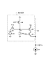
図1は、本開示の第1実施形態に係る固体撮像装置、例えばX−Yアドレス方式固体撮像装置の一種であるCMOSイメージセンサの構成の概略を示すシステム構成図である。ここで、CMOSイメージセンサとは、CMOSプロセスを応用して、または、部分的に使用して作成されたイメージセンサである。
<1. First Embodiment>
[1-1. System configuration]
FIG. 1 is a system configuration diagram illustrating an outline of a configuration of a solid-state imaging device according to the first embodiment of the present disclosure, for example, a CMOS image sensor which is a kind of an XY address type solid-state imaging device. Here, the CMOS image sensor is an image sensor created by applying or partially using a CMOS process.
図1に示すように、本実施形態に係るCMOSイメージセンサ10Aは、単位画素11が行列状に2次元配置されてなる画素アレイ部12と、当該画素アレイ部12の各画素11を駆動する周辺の駆動系及び信号処理系を有する。本例では、周辺の駆動系や信号処理系として、例えば、行走査部13、カラム処理部14A、参照信号生成部15、列走査部16、水平出力線17、及び、タイミング制御部18が設けられている。これらの駆動系及び信号処理系は、画素アレイ部12と同一の半導体基板(チップ)19上に集積されている。
As shown in FIG. 1, the CMOS image sensor 10 A according to the present embodiment drives a
このシステム構成において、タイミング制御部18は、マスタークロックMCKに基づいて、行走査部13、カラム処理部14A、参照信号生成部15、及び、列走査部16などの動作の基準となるクロック信号や制御信号などを生成する。タイミング制御部18で生成されたクロック信号や制御信号などは、行走査部13、カラム処理部14A、参照信号生成部15、及び、列走査部16などに対してそれらの駆動信号として与えられる。
In this system configuration, the
画素アレイ部12は、受光した光量に応じた光電荷を生成し、かつ、蓄積する光電変換部を有する単位画素(以下、単に「画素」と記述する場合もある)11が行方向及び列方向に、即ち、行列状に2次元配置された構成となっている。ここで、行方向とは画素行の画素の配列方向(即ち、水平方向/横方向)を言い、列方向とは画素列の画素の配列方向(即ち、垂直方向/縦方向)を言う。
The
この画素アレイ部12において、行列状の画素配置に対して、画素行毎に行制御線21(21-1〜21-n)が行方向に沿って配線され、画素列ごとに列信号線22(22-1〜22-m)が列方向に沿って配線されている。行制御線21は、単位画素11から読み出す際の制御を行うための制御信号を伝送する。図1では、行制御線21について1本の配線として示しているが、1本に限られるものではない。行制御線21-1〜21-nの各一端は、行走査部13の各行に対応した各出力端に接続されている。
In this
行走査部13は、シフトレジスタやアドレスデコーダなどによって構成され、画素アレイ部12の各画素11を全画素同時あるいは行単位等で駆動する。すなわち、行走査部13は、当該行走査部13を制御するタイミング制御部18と共に、画素アレイ部12の各画素11を駆動する駆動部を構成している。この行走査部13はその具体的な構成については図示を省略するが、一般的に、読出し走査系と掃出し走査系の2つの走査系を有する構成となっている。
The
読出し走査系は、単位画素11から信号を読み出すために、画素アレイ部12の単位画素11を行単位で順に選択走査する。単位画素11から読み出される信号はアナログ信号である。掃出し走査系は、読出し走査系によって読出し走査が行われる読出し行に対して、その読出し走査よりもシャッタスピードの時間分だけ先行して掃出し走査を行う。
The readout scanning system selectively scans the
この掃出し走査系による掃出し走査により、読出し行の単位画素11の光電変換部から不要な電荷が掃き出されることによって当該光電変換部がリセットされる。そして、この掃出し走査系によって不要電荷を掃き出す(リセットする)ことにより、所謂、電子シャッタ動作が行われる。ここで、電子シャッタ動作とは、光電変換部の光電荷を捨てて、新たに露光を開始する(光電荷の蓄積を開始する)動作のことを言う。
By the sweep scanning by the sweep scanning system, unnecessary charges are swept out from the photoelectric conversion unit of the
読出し走査系による読出し動作によって読み出される信号は、その直前の読出し動作または電子シャッタ動作以降に受光した光量に対応するものである。そして、直前の読出し動作による読出しタイミングまたは電子シャッタ動作による掃出しタイミングから、今回の読出し動作による読出しタイミングまでの期間が、単位画素11における光電荷の露光期間となる。
The signal read by the reading operation by the reading scanning system corresponds to the amount of light received after the immediately preceding reading operation or electronic shutter operation. The period from the read timing by the immediately preceding read operation or the sweep timing by the electronic shutter operation to the read timing by the current read operation is the photo charge exposure period in the
カラム処理部14Aは、例えば、画素アレイ部12の画素列毎、即ち、列信号線22(22-1〜22-m)毎に1対1の対応関係をもって設けられたAD(アナログ−デジタル)変換回路23(23-1〜23-m)を有する。AD変換回路23(23-1〜23-m)は、画素アレイ部12の各単位画素11から画素列毎に出力されるアナログ信号(画素信号)をデジタル信号に変換する。
Column processing section 14 A, for example, each pixel column of the
参照信号生成部15は、時間が経過するにつれて電圧値が階段状に変化する、所謂、ランプ(RAMP)波形(傾斜状の波形)の参照信号Vrefを生成する。参照信号生成部15については、例えば、DAC(デジタル−アナログ変換)回路を用いて構成することができる。尚、参照信号生成部15としては、DAC回路を用いた構成のものに限られるものではない。
The
参照信号生成部15は、タイミング制御部18から与えられる制御信号CS1による制御の下に、当該タイミング制御部18から与えられるクロックCKに基づいてランプ波の参照信号Vrefを生成する。そして、参照信号生成部15は、生成した参照信号Vrefをカラム処理部15のAD変換回路23-1〜23-mに対して供給する。
The reference
AD変換回路23-1〜23-mは全て同じ構成となっている。ここでは、m列目のAD変換回路23-mを例に挙げて説明するものとする。AD変換回路23-mは、比較器31、カウント部である例えばアップ/ダウンカウンタ(図中、「U/DCNT」と記している)32、転送スイッチ33、及び、メモリ装置34を有する構成となっている。
The
比較器31は、画素アレイ部12のn列目の各単位画素11から出力される画素信号に応じた列信号線22-mの信号電圧Voutを比較入力とし、参照信号生成部15から供給されるランプ波の参照信号Vrefを基準入力とし、両者を比較する。そして、比較器31は、例えば、参照信号Vrefが信号電圧Voutよりも大なるときに出力Vcoが第1の状態(例えば、高レベル)になり、参照信号Vrefが信号電圧Vx以下のときに出力Vcoが第2の状態(例えば、低レベル)になる。
The comparator 31 receives the signal voltage V out of the
アップ/ダウンカウンタ32は非同期カウンタであり、タイミング制御部18から与えられる制御信号CS2による制御の下に、当該タイミング制御部18からクロックCKが参照信号生成部15と同じタイミングで与えられる。そして、アップ/ダウンカウンタ32は、クロックCKに同期してダウン(DOWN)カウント、または、アップ(UP)カウントを行うことで、比較器31での比較動作の開始から比較動作の終了までの比較期間を計測する。
The up / down
転送スイッチ33は、タイミング制御部18から与えられる制御信号CS3による制御の下に、ある画素行の単位画素11についてのアップ/ダウンカウンタ32のカウント動作が完了した時点でオン(閉)状態となる。そして、転送スイッチ33は、アップ/ダウンカウンタ32のカウント結果をメモリ装置34に転送する。
The transfer switch 33 is turned on (closed) when the count operation of the up / down counter 32 for the
このようにして、画素アレイ部12の各単位画素11から列信号線22-1〜22-mを経由して画素列毎に供給されるアナログ信号について、AD変換回路23(23-1〜23-m)において先ず比較器31で比較動作が行われる。そして、アップ/ダウンカウンタ32において、比較器31での比較動作の開始から比較動作の終了までの期間に亘ってカウント動作を行うことで、アナログ信号がデジタル信号に変換されてメモリ装置34に格納される。
In this manner, the AD conversion circuit 23 (23 −1 to 23) is used for analog signals supplied from the
列走査部16は、シフトレジスタやアドレスデコーダなどによって構成され、カラム処理部14AにおけるAD変換回路23-1〜23-mの列アドレスや列走査の制御を行う。この列走査部16による制御の下に、AD変換回路23-1〜23-mの各々でAD変換されたデジタル信号は順に水平出力線17に読み出され、当該水平出力線17を経由して撮像データとして出力される。
The
尚、本開示には直接関連しないため特に図示しないが、水平出力線17を経由して出力される撮像データに対して各種の信号処理を施す回路等を、上記構成要素以外に設けることも可能である。その際、これらの回路が画素アレイ部12と同一の半導体基板19上に設けられているか否かは問わない。
Although not specifically shown because it is not directly related to the present disclosure, a circuit for performing various signal processing on imaging data output via the horizontal output line 17 may be provided in addition to the above-described components. It is. At this time, it does not matter whether these circuits are provided on the
上記構成の列並列ADC搭載のCMOSイメージセンサ10Aは、画素アレイ部12中の全画素11に対して同一のタイミングで露光開始と露光終了とを実行するグローバル露光も可能としている。このグローバル露光は、行走査部13及びタイミング制御部18からなる駆動部による駆動の下に実行される。グローバル露光を実現するグローバルシャッタ機能は、高速に動く被写体の撮像や、撮像画像の同時性を必要とするセンシング用途に用いて好適なシャッタ動作である。
The CMOS image sensor 10 A equipped with the column-parallel ADC having the above-described configuration can also perform global exposure in which the exposure start and the exposure end are executed at the same timing for all the
尚、本例では、カラム処理部14Aについて、AD変換回路23が列信号線22毎に1対1の対応関係をもって設けられた構成を例に挙げたが、1対1の対応関係の配置に限られるものではない。例えば、1つのAD変換回路23を複数の画素列で共有し、複数の画素列間で時分割にて使用する構成を採ることも可能である。
In this example, the column processing unit 14 A has a configuration in which the
[1−2.画素構成]
図2は、単位画素11の構成の一例を示す回路図である。図2に示すように、本構成例に係る単位画素11は、光電変換部として例えばフォトダイオード41を有している。単位画素11は、フォトダイオード41に加えて、例えば、電荷検出部42、転送トランジスタ(転送ゲート部)43、リセットトランジスタ44、増幅トランジスタ45、及び、選択トランジスタ46を有する構成となっている。
[1-2. Pixel configuration]
FIG. 2 is a circuit diagram illustrating an example of the configuration of the
尚、ここでは、転送トランジスタ43、リセットトランジスタ44、増幅トランジスタ45、及び、選択トランジスタ46として、例えばNチャネル型のMOSトランジスタを用いている。但し、ここで例示した転送トランジスタ43、リセットトランジスタ44、増幅トランジスタ45、及び、選択トランジスタ46の導電型の組み合わせは一例に過ぎず、これらの組み合わせに限られるものではない。
Here, as the
この単位画素11に対して、先述した行制御線21(21-1〜21-n)として、複数の制御線が同一画素行の各画素に対して共通に配線される。図2では、図面の簡略化のために、複数の制御線については図示を省略している。複数の制御線は、行走査部13の各画素行に対応した出力端に画素行単位で接続されている。行走査部13は、複数の制御線に対して転送信号TRG、リセット信号RST、及び、選択信号SELを適宜出力する。
For the
フォトダイオード41は、アノード電極が負側電源(例えば、グランド)に接続されており、受光した光をその光量に応じた電荷量の光電荷(ここでは、光電子)に光電変換してその光電荷を蓄積する。フォトダイオード41のカソード電極は、転送トランジスタ43を介して増幅トランジスタ45のゲート電極と電気的に接続されている。
The
増幅トランジスタ45のゲート電極と電気的に繋がった領域は、電荷を電圧に変換する電荷検出部42である。以下、電荷検出部42をFD(フローティング・ディフュージョン/浮遊拡散領域/不純物拡散領域)部42と呼ぶ。
A region electrically connected to the gate electrode of the
転送トランジスタ43は、フォトダイオード41のカソード電極とFD部42との間に接続されている。転送トランジスタ43のゲート電極には、高レベル(例えば、Vddレベル)がアクティブ(以下、「Highアクティブ」と記述する)となる転送信号TRGが行走査部13から与えられる。転送トランジスタ43は、転送信号RGに応答して導通状態となることで、フォトダイオード41で光電変換され、蓄積された光電荷をFD部42に転送する。
The
リセットトランジスタ44は、ドレイン電極がリセット電源Vrに、ソース電極がFD部42にそれぞれ接続されている。リセットトランジスタ44のゲート電極には、Highアクティブのリセット信号RSTが行走査部13から与えられる。リセットトランジスタ44は、リセット信号RSTに応答して導通状態となり、FD部42の電荷をリセット電源Vrに捨てることによって当該FD部42をリセットする。
The
増幅トランジスタ45は、ゲート電極がFD部42に、ドレイン電極が画素電源Vddにそれぞれ接続されている。この増幅トランジスタ45は、フォトダイオード41での光電変換によって得られる信号を読み出す読出し回路であるソースフォロワの入力部となる。すなわち、増幅トランジスタ45は、ソース電極が選択トランジスタ46を介して列信号線22に接続されることで、当該列信号線22の一端に接続される電流源24とソースフォロワを構成する。
The
選択トランジスタ46は、例えば、ドレイン電極が増幅トランジスタ45のソース電極に、ソース電極が列信号線22にそれぞれ接続されている。選択トランジスタ46のゲート電極には、Highアクティブの選択信号SELが行走査部13から与えられる。選択トランジスタ46は、選択信号SELに応答して導通状態となることで、単位画素11を選択状態として増幅トランジスタ45から出力される信号を列信号線22に伝達する。
For example, the
尚、選択トランジスタ46については、画素電源Vddと増幅トランジスタ45のドレイン電極との間に接続した回路構成を採ることも可能である。
The
[1−3.相関二重サンプリングによるノイズ除去処理]
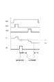
上記構成の単位画素11が行列状に2次元配置されて構成される固体撮像装置では、一般的に、リセット動作時のノイズを除去するために、相関二重サンプリングによるノイズ除去処理が行わる。図3に示すように、選択信号SELによって選択された状態にある単位画素11は、リセット信号RSTに応答してFD部42をリセット電位Vrにリセットし、当該リセット電位VrをリセットレベルVrstとして読み出す。続いて、転送信号TRGによって転送トランジスタ43を駆動し、フォトダイオード41に蓄積された電荷をFD部42へ転送し、当該電荷を信号レベルVsigとして読み出す。
[1-3. Noise removal processing by correlated double sampling]
In the solid-state imaging device configured by two-dimensionally arranging the
リセットレベルVrst及び信号レベルVsigには、熱雑音、寄生容量のカップリングによる雑音といった、リセット毎にランダムに発生するノイズ(Random Noise)が、FD部42をリセット電位Vrにリセットした際に加わっている。これらのノイズとしては、FD部42をリセットする度に異なるノイズが加わる。
In the reset level V rst and the signal level V sig , noise (Random Noise) randomly generated at each reset such as thermal noise and noise due to parasitic capacitance coupling resets the
リセットレベルVrstを先に読み出す読み出し方式においては、リセットしたときに発生するランダムノイズはFD部42で保持されているため、信号電荷を加えて読み出された信号レベルVsigには、リセットレベルVrstと同じノイズ量が保持されている。このため、信号レベルVsigからリセットレベルVrstを減算する相関二重サンプリング動作を行うことで、これらのノイズを除去した信号を得ることが可能となる。
In the readout method in which the reset level V rst is read first, random noise generated at the time of resetting is held in the
すなわち、相関二重サンプリング動作では、信号電荷をFD部42へ転送する前に、FD部42をリセットしてリセットレベルを読み出すことが、これらのリセットノイズを除去できる条件となる。また、信号の読み出しに用いられる増幅トランジスタ45の閾値ばらつき等、固定的に加わるノイズ(固定パターンノイズ;Fixed Pattern Noise)も除去することができる。
That is, in the correlated double sampling operation, before the signal charge is transferred to the
単位画素11から読み出されたリセットレベルVrst及び信号レベルVsigは、AD変換回路23においてデジタル信号に変換される。一般的に、AD変換回路23の変換可能な入力電圧の範囲には制限があるため、単位画素11から出力されるアナログ信号を、AD変換回路23の入力電圧範囲に収まるよう設計する必要がある。
The reset level V rst and the signal level V sig read from the
すなわち、リセットレベルVrstから、取得すべき信号レベルVsigまでの電圧範囲が、AD変換回路23の入力電圧範囲内に収まっている必要がある。例えば、リセットレベルVrstが3Vで、信号電荷による出力の振幅が−1Vであったとすると、取得すべき最大の信号レベルが2Vとなる。この場合、AD変換回路23の変換可能な入力電圧範囲は2V〜3Vであればよいことになる。
That is, the voltage range from the reset level V rst to the signal level V sig to be acquired needs to be within the input voltage range of the
しかし、実際には、増幅トランジスタ45の閾値ばらつきや、列信号線22との間の寄生容量によるオフセット等で、リセットレベルVrstは画素毎に異なっている。例えば、2次元配置された単位画素11のリセットレベルVrstの平均値は3Vであっても、単位画素11によって3.1Vや2.9VのリセットレベルVrstを出力する可能性がある。この場合、信号電荷による振幅の幅が一様に−1Vであったとしても、AD変換回路23は1.9V〜3.1Vの入力電圧を変換可能でなくてはいけない。AD変換回路23の変換可能な入力電圧範囲を広げることは、即ち、AD変換回路23の基本性能を高めることに他ならず、電源電圧、消費電力、面積などが増加する要因となる。
However, in practice, the reset level V rst varies from pixel to pixel due to variations in threshold value of the
このことから、AD変換回路23の変換可能な入力電圧範囲の幅は、信号電荷による出力の振幅に近づけることが好ましい。そのため、AD変換回路23の入力電圧範囲の基準となる基準電圧を調整する方法が採られる。基準電圧によってAD変換回路23の入力電圧範囲をシフトさせることで、画素の出力信号、即ち、AD変換回路23の入力信号のオフセット成分を除去し、リセットレベルVrstのばらつきによる必要な入力電圧範囲の拡大を回避することが可能となる。
For this reason, the width of the input voltage range that can be converted by the
[1−4.従来技術の説明]
特許文献1に記載の従来技術では、図4に示すように、単位画素11から先に読み出されるリセットレベルVrstを、制御信号ΦRによる制御の下に、AD変換回路23の基準電圧Vzrとして設定し、リセットレベルVrst及び信号レベルVsigをAD変換するようにしている。このように、基準電圧VzrをリセットレベルVrstと等しくすることで、リセットレベルVrstがノイズによって変動しても、信号電荷による単位画素11の出力振幅|Vsig−Vrst|を安定してAD変換回路23の入力電圧範囲に収めることが可能となる。
[1-4. Description of prior art]
In the prior art described in
前にも述べたように、AD変換回路23の基準電圧Vzrは、一般的に、AD変換回路23の入力電圧範囲に対して十分小さい範囲でしか調整できない。従って、AD変換回路23の基準電圧Vzrとしては、リセットレベルVrstのように、ばらつきの幅が安定して限られている信号が好ましい。逆に、信号レベルVsigのように入射光量によって電圧が大きく振幅する信号は、AD変換回路23の基準電圧Vzrとしては適さない。
As described above, the reference voltage V zr of the
このように、特許文献1に記載の従来技術では、ノイズ除去処理に際して、単位画素11から先にリセットレベルVrstを読み出し、当該リセットレベルVrstの直後に信号レベルVsigを読み出すことが前提となっている。
Thus, in the conventional technique described in
[1−5.第1実施形態の前提となる構成]
これに対して、第1実施形態に係るCMOSイメージセンサ10Aは、全画素一括露光のために、信号電荷をFD部42に保持した状態で信号読み出しを実行する構成を採っている。すなわち、第1実施形態に係るCMOSイメージセンサ10Aは、リセットレベルVrstを信号レベルVsigの直前に読み出すことができない構成となっている。従って、上述した考えの下では、単位画素11の信号レベルVsigをAD変換する前に同一画素から基準電圧Vzrを取得することができないことになる。
[1-5. Configuration as a premise of the first embodiment]
On the other hand, the CMOS image sensor 10 A according to the first embodiment adopts a configuration in which signal readout is performed in a state where the signal charge is held in the
一方で、全画素一括露光を実現するCMOSイメージセンサ10Aにおいては、基本的には1行毎に、単位画素11から信号を読み出す動作が2回行われる。2回の読み出し動作を行う前提として、単位画素11が、光電変換された電荷量が所定の電荷量を超えたときに、当該所定の飽和電荷量を超えた信号電荷がFD部42に蓄積される画素構造となっているものとする。
On the other hand, in the CMOS image sensor 10 A that realizes all-pixel batch exposure, basically, an operation of reading a signal from the
尚、本明細書においては、光電変換された電荷量が所定の電荷量を超える光が入射されるときを「高照度」と呼び、光電変換された電荷量が所定の電荷量以下となる光が入射されるときを「低照度」と呼ぶこととする。 In this specification, when light whose photoelectric charge amount exceeds a predetermined charge amount is incident, it is called “high illuminance”, and light whose photoelectric charge amount is equal to or less than a predetermined charge amount. Will be referred to as “low illumination”.
2回の読み出し動作のうち1回目の読み出し動作では、FD部42に保持、もしくは、蓄積されている信号電荷を信号レベルとして読み出し、次いで、FD部42を所定電位にリセットして当該所定電位をリセットレベルとして読み出す駆動(第1の駆動)が行われる。以下では、1回目の駆動を、「DDS(Double Data Sampling)駆動」と呼ぶこととする。このDDS駆動では、単位画素11から先に読み出される信号レベルを、AD変換回路23の変換可能な入力電圧範囲の基準となる基準電圧として用いる。
In the first read operation out of the two read operations, the signal charge held or accumulated in the
2回目の読み出し動作では、FD部42を所定電位にリセットして当該所定電位をリセットレベルとして読み出した後、フォトダイオード41に蓄積されている信号電荷をFD部42に転送し、次いで、FD部42の信号電荷を信号レベルとして読み出す駆動(第2の駆動)が行われる。以下では、2回目の駆動を、「CDS(Correlated Double Sampling)駆動」と呼ぶこととする。このCDS駆動では、単位画素11から先に読み出されるリセットレベルを、AD変換回路23の変換可能な入力電圧範囲の基準となる基準電圧として用いる。
In the second read operation, after resetting the
ここで、DDS駆動とCDS駆動とを併用する理由について説明する。先述したことから明らかなように、FD部42を信号保持、もしくは、蓄積部として用いることで、FD部42を用いない場合に比較して信号のダイナミックレンジを拡大することができる。但し、DDS駆動では、信号レベルの読み出しとリセットレベルの読み出しとの間にリセット動作が介在するため、先に読み出される信号レベルに含まれるリセットレベルと、後で読み出されるリセットレベルとの間の相関が低い。
Here, the reason why the DDS drive and the CDS drive are used together will be described. As is clear from the above description, by using the
これに対して、CDS駆動では、リセット動作を行った後に、リセットレベルと信号レベルとを連続して読み出すため、先に読み出されるリセットレベルと、後で読み出される信号レベルに含まれるリセットレベルとの間の相関が高い。従って、DDS駆動に比べてCDS駆動の方が確実にノイズ除去を行うことができるため高画質化を図る上で有利である。このような理由から、グローバル露光を実現しつつ高画質化を図るには、DDS駆動単独の駆動法よりも、DDS駆動とCDS駆動とを併用する駆動法の方が好ましい。 On the other hand, in the CDS drive, the reset level and the signal level are continuously read after the reset operation is performed. Therefore, the reset level read first and the reset level included in the signal level read later are Correlation between is high. Therefore, the CDS drive is more advantageous in achieving higher image quality than the DDS drive because noise can be reliably removed. For this reason, in order to achieve high image quality while realizing global exposure, a driving method using both DDS driving and CDS driving is preferable to a driving method using only DDS driving.
ところで、DDS駆動では、単位画素11から先に読み出される信号レベルをAD変換回路23の基準電圧として用いるとしているが、前にも述べたように、入射光量によって電圧が大きく振幅する信号レベルは、本来ならば、AD変換回路23の基準電圧としては適さない。信号レベルをAD変換回路23の基準電圧として用いる場合、AD変換回路23の入力段を構成する比較器31の動作範囲の確保の問題を解消する必要がある。この問題について詳しく説明する。その前に、AD変換回路23の入力段を構成する比較器31の従来構成について説明する。
By the way, in the DDS drive, the signal level read out first from the
(AD変換回路の入力段を構成する比較器の従来構成について)
図5は、AD変換回路の入力段を構成する比較器の従来構成についての説明図であり、(A)は比較器の構成例を、(B)は比較器の動作範囲をそれぞれ示している。
(Regarding the conventional configuration of the comparator constituting the input stage of the AD conversion circuit)
FIG. 5 is an explanatory diagram of a conventional configuration of a comparator constituting the input stage of the AD conversion circuit, where (A) shows a configuration example of the comparator and (B) shows an operation range of the comparator. .
図5(A)に示すように、従来構成に係る比較器31は、ソース電極が共通に接続された差動対トランジスタ(コンパレータトランジスタ)51,52と、そのソース共通ノードとグランドとの間に接続された電流源53とを有している。差動対トランジスタ51,52として、Nチャネル型のMOSトランジスタ(以下、「NMOSトランジスタ」と記述する)が用いられている。
As shown in FIG. 5A, a comparator 31 according to the conventional configuration includes a differential pair transistor (comparator transistor) 51 and 52 having source electrodes connected in common, and a common source node between the source and the ground. And a connected
NMOSトランジスタ51のゲート電極には、参照信号生成部15で生成される傾斜状波形(階段波)の参照信号Vrefiが容量54を介して与えられる。NMOSトランジスタ52のゲート電極には、単位画素11から列信号線22-mを通して供給される信号電圧Voutが容量55を介して与えられる。
A reference signal V refi having an inclined waveform (staircase wave) generated by the reference
NMOSトランジスタ51のドレイン電極と電源Vddとの間にはダイオード接続構成、即ち、ゲート電極とドレイン電極とが共通に接続されたPチャネル型のMOSトランジスタ(以下、「PMOSトランジスタ」と記述する)56が接続されている。NMOSトランジスタ52のドレイン電極と電源Vddとの間には、PMOSトランジスタ57が接続されている。PMOSトランジスタ56,57は、ゲート電極が互いに共通に接続されている。
A diode-connected configuration between the drain electrode of the
NMOSトランジスタ51のゲート電極とドレイン電極との間にはPMOSトランジスタ58が接続されている。NMOSトランジスタ52のゲート電極とドレイン電極との間にも、PMOSトランジスタ59が接続されている。そして、これらPMOSトランジスタ58,59の各ゲート電極には、基準電圧を設定するための制御を行う制御信号ΦRの反転信号xΦRが印加される。
A
上記の従来構成に係る比較器31において、AD変換回路23の基準電圧は、制御信号ΦRの反転信号xΦRがPMOSトランジスタ58,59の各ゲート電極に印加されることによって容量54,55に保持される。そして、比較器31において、参照信号Vrefと列信号線22-mの信号電圧Voutとが比較される。具体的には、参照信号Vrefの変化に応じて、信号電圧Voutとの比較結果(比較出力)Vcoが遷移するタイミングをデジタル信号として保持する。
In the comparator 31 according to the above-described conventional configuration, the reference voltage of the
制御信号ΦRの反転信号xΦRによって取得された基準電圧に対して、参照信号Vref及び信号電圧Voutがそれぞれ同じ振幅となったときに比較出力Vcoが遷移する。図5(B)において、VthはMOSトランジスタの閾値電圧であり、ΔVは単位画素11のリセットレベルと信号レベルとの電位差である。尚、本開示が適用されるAD変換回路23は、入力電圧範囲を調整する基準電圧の設定手段を有していれば、本構成に限るものではない。
The control signal Φ inverted signal Xfai R acquired by the reference voltage of the R, the comparison output V co transitions when a reference signal V ref and the signal voltage V out becomes the same amplitude, respectively. In FIG. 5B, V th is the threshold voltage of the MOS transistor, and ΔV is the potential difference between the reset level and the signal level of the
図6に、CDS駆動時の比較器31の内部ノードの電圧、及び、そのときの動作範囲を示す。また、図7及び図8に、DDS駆動時の低照度時、高照度時の比較器31の内部ノードの電圧、及び、そのときの動作範囲を示す。図6乃至図8に示すように、基準電圧を設定する期間(図中、AZの期間)の電圧は、図5の比較器31の入出力電圧をPMOSトランジスタ58,59にてショートした電圧となる。 FIG. 6 shows the voltage of the internal node of the comparator 31 during CDS driving and the operating range at that time. 7 and 8 show the voltage of the internal node of the comparator 31 at the time of low illuminance and high illuminance during DDS driving, and the operation range at that time. As shown in FIGS. 6 to 8, the voltage in the period for setting the reference voltage (period AZ in the figure) is the voltage obtained by shorting the input / output voltage of the comparator 31 in FIG. Become.
図6乃至図8において、○印は、比較器31の2つの入力、即ち、画素信号に応じた列信号線22-mの信号電圧Voutにより変位するNMOSトランジスタ52のゲート電極側の電位Voutiと、参照信号生成部15から供給されるランプ波の参照信号Vrefにより変位する、NMOSトランジスタ51のゲート電極側の電位Vrefiとが一致するポイントを示している。以下の動作範囲を示す図でも同様とする。
6 to 8, the circles indicate the potential V on the gate electrode side of the
図6に示すCDS駆動の場合は、参照信号Vrefが比較器31の動作範囲内に収まる。これに対して、図7及び図8に示すDDS駆動の場合は、リセットレベルは信号レベルよりも高いために、比較のための参照信号Vrefについては、信号レベルを読んだ場合よりも高い電圧とする必要がある。このとき、比較器31に入力される参照信号Vrefの電圧は比較器31の動作範囲を超えてしまうため、比較器31が動作しない。 In the case of CDS driving shown in FIG. 6, the reference signal V ref falls within the operation range of the comparator 31. On the other hand, in the case of the DDS drive shown in FIGS. 7 and 8, since the reset level is higher than the signal level, the reference signal V ref for comparison has a higher voltage than when the signal level is read. It is necessary to. At this time, the voltage of the reference signal V ref input to the comparator 31 exceeds the operation range of the comparator 31, so the comparator 31 does not operate.
参照信号Vrefが比較器31の動作範囲を超えてしまうことについては、図9(A),(B)に示すように、参照信号Vrefの傾斜を上下逆にしても同じである。従って、比較器31の動作範囲の確保の問題については根本的に解決することはできない。図9において、(A)は低照度時、(B)は高照度時をそれぞれ示している。 The fact that the reference signal V ref exceeds the operation range of the comparator 31 is the same even if the inclination of the reference signal V ref is turned upside down, as shown in FIGS. Therefore, the problem of ensuring the operating range of the comparator 31 cannot be fundamentally solved. In FIG. 9, (A) shows a low illuminance, and (B) shows a high illuminance.
また、図10に示すように、比較器31に関して、NMOSトランジスタとPMOSトランジスタとを入れ替えた回路構成を採る方法も考えられる。図10において、(A)はPMOS入力の比較器の構成例を、(B)はPMOS入力の比較器の動作範囲をそれぞれ示している。 Further, as shown in FIG. 10, a method of adopting a circuit configuration in which the NMOS transistor and the PMOS transistor are interchanged with respect to the comparator 31 is also conceivable. 10A shows a configuration example of a PMOS input comparator, and FIG. 10B shows an operation range of the PMOS input comparator.
しかし、図10の回路構成は、CDS駆動の動作範囲を確保できず、CDS駆動を行うことができないことになる。比較器31として2種類、即ち、図5(A)に示す回路構成のもの、及び、図10(A)に示す回路構成のものの双方を用意して、DDS駆動とCDS駆動とで使い分ける方法も考えられる。この方法の場合には、CDS駆動用の回路と併せて回路規模が2倍になるため、コスト増を招くことと、2種類の異なる回路を用いるため特性のばらつきの問題が発生する。 However, the circuit configuration of FIG. 10 cannot ensure the CDS driving operation range and cannot perform CDS driving. There are two types of comparators 31, that is, those having the circuit configuration shown in FIG. 5A and those having the circuit configuration shown in FIG. 10A, and a method of selectively using DDS driving and CDS driving. Conceivable. In the case of this method, the circuit scale is doubled together with the circuit for driving the CDS, which causes an increase in cost and causes a problem of variation in characteristics due to the use of two different types of circuits.
[1−6.第1実施形態の特徴とする事項]
そこで、第1実施形態では、単位画素11で得られるアナログ信号と傾斜状波形の参照信号Vrefとを比較する比較器31を有するAD変換回路23を備えたCMOSイメージセンサ10Aにおいて、次の構成を採ることを特徴とする。
[1-6. Matters Characteristic of First Embodiment]
Therefore, in the first embodiment, in the CMOS image sensor 10 A including the
具体的には、先ず、単位画素11の信号を第1の信号及び第2の信号として2回に分けて読み出す際に、先に読み出される第1の信号を、第1,第2の信号を処理する信号処理部の処理可能な入力電圧範囲の基準電圧として用いる。本実施形態の場合は、AD変換回路23が、第1,第2の信号を処理する信号処理部に相当する。また、基準電圧は、AD変換回路23の変換可能な入力電圧範囲の基準となる電圧となる。本実施形態では、比較器31の動作範囲がAD変換回路23の入力電圧範囲ということになる。
Specifically, first, when the signal of the
このとき、第1の信号がFD部42に蓄積、もしくは、保持された信号電荷に基づく信号、即ち、信号レベルVsigである場合には、当該信号レベルVsigを基準電圧として用いることになる。また、第1の信号がFD部42をリセットしたときのリセット電位Vrに基づく信号、即ち、リセットレベルVrstである場合には、当該リセットレベルVrstを基準電圧として用いることになる。そして、先に読み出される第1の信号をAD変換回路23の基準電圧として用いた上で、第1,第2の信号がAD変換回路23の入力電圧範囲内に入るようにAD変換回路23の内部の基準電圧、即ち、トランジスタ51,52のゲート電圧Vouti,Vrefiの初期値を調整した状態で第1,第2の信号に対してAD変換処理を施すようにする。
In this case, accumulation first signal to the
このように、第1,第2の信号がAD変換回路23の入力電圧範囲内に入るように調整することで、AD変換回路23は、第1,第2の信号が入力電圧範囲内に入った状態でこれら第1,第2の信号に対してAD変換処理を実行することが可能になる。従って、先に読み出される第1の信号が信号レベルVsigの場合、リセットレベルVrstの場合のいずれの場合にも、処理対象の画素の信号を用いて基準電圧を設定した上で、第1,第2の信号に対して確実にAD変換処理を施すことができることとなる。
Thus, by adjusting the first and second signals so that they fall within the input voltage range of the
これにより、特許文献5に記載の従来技術、即ち、別途外部で生成した所定電圧を用いて基準電圧を設定する場合のような、面内の大きな特性の揺らぎ(面内分布)の差異や、寄生容量の大きさに依存したオフセット成分を効果的に除去できる。その結果、画素の出力振幅に対して、AD変換回路23の変換可能な入力電圧範囲に必要なマージンを低減することが可能となる。そして、当該入力電圧範囲に必要なマージンを低減できることにより、AD変換回路23の電源電圧の低電圧化や低消費電力化を図ることができる。
Thereby, the conventional technique described in Patent Document 5, that is, a difference in fluctuation (in-plane distribution) of large in-plane characteristics, such as when a reference voltage is set using a predetermined voltage separately generated outside, An offset component depending on the size of the parasitic capacitance can be effectively removed. As a result, it is possible to reduce the margin necessary for the input voltage range that can be converted by the
(実施例1)
以下に、具体的な実施例について説明する。前にも述べたように、DDS駆動では、先ず、FD部42に保持、もしくは、蓄積されている信号電荷を信号レベルVsigとして読み出す駆動が行われる。次いで、FD部42をリセット電位Vrにリセットして当該リセット電位VrをリセットレベルVrstとして読み出す駆動が行われる。そして、単位画素11から先に読み出される信号レベルVsigを、AD変換回路23の変換可能な入力電圧範囲の基準となる基準電圧として用いる。換言すれば、先に読み出される信号レベルVsigを用いてAD変換回路23の内部の基準電圧Vouti,Vrefiを設定する。
Example 1
Specific examples will be described below. As described above, in the DDS drive, first, a drive for reading the signal charge held or accumulated in the
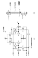
図11は、AD変換回路23の内部の基準電圧Vouti,Vrefiを調整する機能を備えた、実施例1に係る比較器についての説明図であり、(A)は当該比較器の構成例を、(B)は当該比較器の動作範囲をそれぞれ示している。図11において、図5と同等部位には同一符号を付して示している。
FIG. 11 is an explanatory diagram of the comparator according to the first embodiment having a function of adjusting the reference voltages V outi and V refi inside the
図11(A)に示すように、実施例1に係る比較器31Aは、NMOSトランジスタ51,52,56,57、PMOSトランジスタ58,59、電流源53、及び、容量54,55に加えて、AD変換回路23の内部の基準電圧Vouti,Vrefiを設定(調整)するための初期電圧設定回路70Aを有する構成となっている。
As shown in FIG. 11A, the comparator 31 A according to the first embodiment includes an
初期電圧設定回路70Aは、外部で設定される外部設定初期電圧Vextが与えられるラインL1とNMOSトランジスタ51,52の各ゲート電極との間に接続されたNMOSトランジスタ71,72によって構成されている。NMOSトランジスタ71,72の各ゲート電極には、制御ラインL2を介して制御信号Φextが与えられる。この制御信号Φextは、例えば、図1に示すタイミング制御部18から与えられる。すなわち、タイミング制御部18は、初期電圧設定回路70Aを制御する制御部としての機能を持っている。
The initial voltage setting circuit 70 A includes
上記構成の比較器31Aにおいて、CDS駆動時は、AD変換回路23の内部の基準電圧Vouti,Vrefiとして、制御信号xΦRの反転信号xΦRに応答してPMOSトランジスタ58,59が導通状態になることによって設定される初期電圧がNMOSトランジスタ51,52のゲート側に保持される。このCDS駆動時の初期電圧、即ち、AD変換回路23の基準電圧は、MOSトランジスタの閾値電圧をVth、単位画素11のリセットレベルVrstと信号レベルVsigとの電位差をΔVとすると、略(Vdd−|Vth+ΔV|)となる。
In the comparator 31 A configured as described above, the
DDS駆動時は、制御信号Φextに応答してNMOSトランジスタ71,72が導通状態になることで、外部設定初期電圧VextがNMOSトランジスタ51,52のゲート電極に与えられる。この外部設定初期電圧Vextにより、比較器31Aの動作範囲が傾斜状波形の参照信号Vrefのスロープの範囲内に入り、当該スロープ内で比較器31Aが動作可能なように、AD変換回路23の内部の基準電圧Vouti,Vrefiの調整が行われる。
During DDS driving, the
このように、DDS駆動時において、初期電圧設定回路70Aの作用により、信号レベルVsig及びリセットレベルVrstがAD変換回路23の入力電圧範囲内に入るように内部の基準電圧Vouti,Vrefiを調整することで、CDS駆動とDDS駆動との両立が可能になる。ここで、信号レベルVsig及びリセットレベルVrstがAD変換回路23の入力電圧範囲内に入るということは、比較器31Aの動作範囲がAD変換回路23の変換可能な入力電圧範囲内に入るということである。
Thus, during DDS driving, the internal reference voltages V outi , V so that the signal level V sig and the reset level V rst fall within the input voltage range of the
また、基準電圧Vouti,Vrefiを設定するための初期電圧設定回路70Aとしては、2つのNMOSトランジスタ71,72を追加するだけの非常に簡単な回路構成で実現できる。従って、比較器31A個々としては、僅かなレイアウト面積の増加で済む。すなわち、CDS駆動とDDS駆動との両立を、比較器31Aのレイアウト面積を僅かに増加するだけで実現できる。
Further , the initial voltage setting circuit 70 A for setting the reference voltages V outi and V refi can be realized with a very simple circuit configuration in which only two
ここで、DDS駆動とCDS駆動とを1行の読み出し期間中に交互に行う場合の動作について説明する。図12及び図13に、DDS駆動とCDS駆動とを交互に行う場合の、DDS駆動の際の低照度時、高照度時の場合の駆動波形をそれぞれ示す。図12及び図13には、制御信号xΦR、制御信号Φext、傾斜状波形の参照信号Vref、及び、単位画素11から列信号線22を介して与えられる信号電圧Voutの波形がそれぞれ示されている。
Here, an operation in the case where DDS driving and CDS driving are alternately performed during the reading period of one row will be described. FIG. 12 and FIG. 13 show driving waveforms in the case of low illuminance and high illuminance during DDS driving, respectively, when DDS driving and CDS driving are alternately performed. In FIGS. 12 and 13, the waveforms of the control signal xΦ R , the control signal Φ ext , the reference signal V ref having an inclined waveform, and the signal voltage V out applied from the
ここでは、参照信号Vrefについて、電圧の時間変化方向が高い側から低い側の場合を例として挙げているが、図9に示すように、電圧の時間変化方向が逆、即ち、低い側から高い側であっても、比較器31Aの動作範囲内であれば、本実施形態のDDS駆動を制限するものではない。また、図10に示すように、PMOS入力で構成した比較器の場合は、初期電圧設定回路70Aについては、図14に示すように、PMOSトランジスタ73,74によって構成するようにすればよい。
Here, the reference signal V ref is exemplified as a case where the time change direction of the voltage is high to low, but as shown in FIG. 9, the time change direction of the voltage is reverse, that is, from the low side. even high side, as long as it is within the operating range of the comparator 31 a, do not limit the DDS drive of the present embodiment. Also, as shown in FIG. 10, in the case of a comparator configured with PMOS inputs, the initial voltage setting circuit 70 A may be configured with
続いて、図11に示す実施例1に係る比較器31Aの回路動作について、図1、図2、及び、図5を参照しつつ図15のタイミング波形図を用いて説明する。 Next, the circuit operation of the comparator 31 A according to the first embodiment shown in FIG. 11 will be described using the timing waveform diagram of FIG. 15 with reference to FIG. 1, FIG. 2, and FIG.
先ず、選択信号SELiに応答して、選択トランジスタ46が導通状態になることにより、i番目(i行目)の単位画素11の選択が行われる。そのとき、FD部42には信号電荷が保持、もしくは、蓄積されている状態にあるものとする。このFD部42の信号電荷に基づく信号レベルVsigを比較器31Aの動作範囲内で検出するために、制御信号Φextがアクティブ状態(高電位の状態)になる。これにより、初期電圧設定回路70Aが動作状態となる。
First, in response to the selection signal SEL i , the
初期電圧設定回路70Aが動作する、即ち、NMOSトランジスタ71,72が導通状態になることで、外部設定初期電圧VextがNMOSトランジスタ51,52に各ゲート電圧Vouti,Vrefiとして印加される。これにより、比較器31Aの入力側の電位が、当該比較器31Aの動作範囲内で信号レベルVsigを取得可能なように、PMOSトランジスタ58,59によって設定される電位よりも低い電位に設定される。この初期電圧設定回路70Aによる動作が、信号レベルVsig及びリセットレベルVrstが比較器31Aの動作範囲内、即ち、AD変換回路23の入力電圧範囲内に入るように基準電圧Vouti,Vrefiを調整する動作である。
When the initial voltage setting circuit 70 A operates, that is, when the
このとき、タイミング制御部18による制御の下に、参照信号生成部15で生成される傾斜状の参照信号Vrefの初期値も、比較器31Aの入力側電位に対応した低い電位に設定(シフト)される。そして、制御信号Φextが非アクティブ状態(低電位の状態)になることで、比較器31Aの入力側の電位、即ち、AD変換回路23の変換可能な入力電圧範囲の基準電圧を調整する動作が完了する。
At this time, under the control of the
この後、タイミング制御部18による制御の下に、参照信号生成部15において、参照信号Vrefを初期状態から、回路のばらつきマージンの取れる範囲で電位をわずかに持ち上げ、スロープ状(傾斜状)に電圧降下させる動作を開始する。そして、比較器31Aの入力電圧間、即ち、単位画素11から読み出された信号レベルVsigと参照信号Vrefとの差分が0になったところで比較器31Aの比較出力Vcoが反転する。
After that, under the control of the
一方、アップ/ダウンカウンタ32は、参照信号Vrefのスロープ開始から例えばアップカウントを開始しており、比較器31Aの比較出力Vcoの反転を受けて、アップカウントを終了する。すなわち、アップ/ダウンカウンタ32は、スロープ開始時点から比較出力Vcoの反転時点までの時間をアップカウントする。このアップカウント動作により、AD変換回路23の基準電圧に対する信号レベルVsigの差を取得することができる。
On the other hand, up / down
次いで、i番目の単位画素11をリセットパルスRSTiにてリセットし、FD部42を初期化する。このとき、リセット前の信号レベルVsigが低ければ、即ち、高輝度であれば、リセット後のFD部42の電位は大きく上昇する。併せて、参照信号Vrefも最大輝度時の信号量であってもスロープがかかるように上昇させる。このとき、アップ/ダウンカウンタ32は、参照信号Vrefのスロープ開始からダウンカウントを行う。そして、比較器31Aの比較出力Vcoの反転を受けて、ダウンカウントを終了する。
Next, the i-
このように、アップ/ダウンカウンタ32のカウント動作を1回目に例えばアップカウント動作とし、2回目に逆方向のダウンカウント動作とすることにより、当該アップ/ダウンカウンタ32内で自動的に(1回目の比較期間)−(2回目の比較期間)の減算処理が行われる。そして、参照信号Vrefと列信号線22-1〜22-mの信号電圧Voutとが等しくなったときに比較器31の比較出力Vcoが極性反転し、この極性反転を受けてアップ/ダウンカウンタ32のカウント動作が停止する。その結果、アップ/ダウンカウンタ32には、(1回目の比較期間)−(2回目の比較期間)の減算処理の結果に応じたカウント値が保持される。
In this way, the counting operation of the up / down
(1回目の比較期間)−(2回目の比較期間)=(信号レベルVsig_i+リセットレベルVrst)−(リセットレベルVrst)=(正味の信号レベルVsig)である。以上の2回の読み出し動作とアップ/ダウンカウンタ32での減算処理により、単位画素11毎のばらつきを含んだリセットレベルVrstが除去されるため、単位画素11毎の入射光量に応じた信号レベルVsigを取り出すことができる。なお、この信号レベルVsigは、限られた照度でより高いダイナミックレンジがとれるよう、外部電圧Vrefのスロープ状の傾きや、信号レベルとリセットレベル間のVref電圧のシフト量とで調整される。
(First comparison period) − (Second comparison period) = (Signal level V sig — i + Reset level V rst ) − (Reset level V rst ) = (Net signal level V sig ) Since the reset level V rst including the variation for each
続いて、CDS駆動に移行する。CDS駆動では、比較器31Aの入出力を制御信号ΦRにて初期化する。この初期化動作により、単位画素11から先に読み出されるリセットレベルVrstを基にAD変換回路23の基準電圧を取得し、容量54,55に保持する。そして、参照信号生成部15において、参照信号Vrefを比較器31Aの動作範囲内で持ち上げてスロープを開始する。
Subsequently, the process shifts to CDS driving. In the CDS drive, the input / output of the comparator 31 A is initialized with the control signal Φ R. By this initialization operation, the reference voltage of the
このとき、参照信号Vrefのスロープ開始時点から比較器31Aの比較出力Vcoの反転時点までの時間を、アップ/ダウンカウンタ32にてダウンカウントする。参照信号Vrefの電圧をスロープ開始位置まで戻し、単位画素11内の転送トランジスタ43を導通状態にすることで、フォトダイオード41に蓄積された信号電荷を読み出す。このとき、フォトダイオード41から読み出された信号電荷の電荷量に応じて列信号線22の電位が変化する。この列信号線22の電位は高照度になるほど降下する。
At this time, the up / down counter 32 counts down the time from the start of the slope of the reference signal V ref to the inversion of the comparison output V co of the comparator 31 A. The voltage of the reference signal V ref is returned to the slope start position, and the
参照信号生成部15において、比較器31Aの動作範囲内で、かつ、単位画素11から読み出される信号をカバーするスロープの参照信号Vrefの生成を開始する。そして、参照信号Vrefのスロープ開始時点から比較器31Aの比較出力Vcoの反転時点までの時間を、アップ/ダウンカウンタ32にてアップカウントする。このアップカウント動作により、FD部42のリセットレベルVrstと、フォトダイオード41からの信号電荷の転送後の信号レベルVsigとの差が検出可能となる。
The reference
ここで、アップ/ダウンカウンタ32のカウント結果の外部への読み出しについては、DDS駆動、CDS駆動で個別にカウントし、メモリ装置34に記憶し外部へ出力してもよいし、連続してカウントしてからメモリ装置34に記憶し外部へ出力してもよい。
Here, regarding the reading of the count result of the up / down counter 32 to the outside, it may be counted individually by DDS driving and CDS driving, stored in the
また、参照信号Vrefのスロープの傾きを変化させることにより、比較器31Aの比較出力Vcoが反転するまでの時間を変化させてゲインをかけることが可能である。このとき、DDS駆動とCDS駆動でスロープの傾きを変え、カウントするときのカウント値に、ゲイン倍の重みをつけてカウントする手法を採ることも可能である。 Further, by changing the slope of the slope of the reference signal V ref , it is possible to apply a gain by changing the time until the comparison output V co of the comparator 31 A is inverted. At this time, it is also possible to change the slope of the slope between DDS driving and CDS driving, and to add a weight that is double the gain to the count value at the time of counting.
また、通常必要とされているCDS駆動の開始時のリセット動作については、電荷検出部であるFD部42がリセットされた直後であるので、再度リセットは必要ないために省いている。但し、暗電流など、FD部42に対する外乱が大きい場合は、DDS駆動とCDS駆動の間でリセット動作をもう一度入れて再初期化することが好ましい。
The reset operation at the start of the CDS drive that is normally required is omitted because the reset operation is not necessary again because it is immediately after the
更に、参照信号生成部15で生成される参照信号Vrefのスロープの方向についても、DDS駆動時とCDS駆動時とで傾き方向を逆にするなどの手法も考えられる。但し、CDS駆動の場合と動作起因の回路の特性ずれが発生しないように、DDS駆動時とCDS駆動時とでスロープの傾き方向を同じ方向にする方が好ましい。
Further, with respect to the direction of the slope of the reference signal V ref generated by the reference
ところで、比較器31Aにおいて、初期設定を行うスイッチ素子であるMOSトランジスタ58,59,71,72から入力部(差動対トランジスタ51,52のゲート)にリーク電流に起因する電流が流れ込み、入力電位の上昇、もしくは、下降が発生する場合がある。このとき、比較器31Aの両入力側でリーク量が同じであれば特性的には問題にならない。しかし、実デバイスにあっては、製造ばらつきなどによって比較器31Aの両入力側のリーク量のバランスが崩れてしまうことがある。
By the way, in the comparator 31 A , current due to leakage current flows from the
この問題については、MOSトランジスタ58,59,71,72のチャネル長Lを長くすることで、これらトランジスタのリーク電流を抑えることができるため解決可能である。しかしながら、チャネル長Lを長くすると、MOSトランジスタ58,59,71,72が非導通状態になるときに発生するクロックフィードスルーとチャージインジェクションが増加し、比較器31Aの特性を劣化させてしまう懸念がある。
This problem can be solved by increasing the channel length L of the
ここで、クロックフィードスルーとは、クロック制御ノードとフローティングノードとの容量比による電圧降下の減少を言う。また、チャージインジェクションとは、MOSトランジスタ58,59,71,72のチャネル直下の電荷のフローティングノードへの飛び込みを言う。クロックフィードスルー及びチャージインジェクションの量は、MOSトランジスタ58,59,71,72の面積に比例する。従って、MOSトランジスタ58,59,71,72のチャネル長Lを長くすると、必然的に、クロックフィードスルー及びチャージインジェクションが大きくなってしまう。
Here, clock feedthrough refers to a decrease in voltage drop due to a capacitance ratio between the clock control node and the floating node. Charge injection refers to the jump of charges immediately below the channels of the
このような理由から、MOSトランジスタ58,59,71,72のリーク電流に起因する、入力電位の上昇、もしくは、下降の問題を解決するために、単純に、これらMOSトランジスタのチャネル長Lを長くすることはできない。そこで、チャネル長Lを長くすることなく、上記の問題を解決するために為されたのが以下に説明する実施例2に係る比較器である。
For this reason, the channel length L of these MOS transistors is simply increased in order to solve the problem of the increase or decrease of the input potential caused by the leakage current of the
(実施例2)
図16は、AD変換回路23の内部の基準電圧Vouti,Vrefiを調整する機能を備えた、実施例2に係る比較器の構成例を示す回路図であり、図中、図11と同等部位には同一符号を付して示している。
(Example 2)
FIG. 16 is a circuit diagram illustrating a configuration example of a comparator according to the second embodiment having a function of adjusting the reference voltages V outi and V refi inside the
図11と図16との対比から明らかなように、実施例2に係る比較器31Bは、初期設定を行うスイッチ素子に関して、実施例1に係る比較器31Aと構成を異にしている。具体的には、実施例1に係る比較器31Aは、初期設定を行うスイッチ素子が単一のMOSトランジスタ58,59,71,72によって構成されている。
As is clear from the comparison between FIG. 11 and FIG. 16, the comparator 31 B according to the second embodiment is different in configuration from the comparator 31 A according to the first embodiment with respect to the switch element that performs the initial setting. Specifically, in the comparator 31 A according to the first embodiment, the switch element that performs the initial setting is configured by a
これに対し、実施例2に係る比較器31Bは、MOSトランジスタ58に代えて直列に接続された2つのMOSトランジスタ58A,58Bを用い、MOSトランジスタ59に代えて直列に接続された2つのMOSトランジスタ59A,5Bを用いた構成を採っている。同様に、MOSトランジスタ71に代えて直列に接続された2つのMOSトランジスタ71A,71Bを用い、MOSトランジスタ72に代えて直列に接続された2つのMOSトランジスタ72A,72Bを用いている。
On the other hand, the comparator 31 B according to the second embodiment uses two
2つのMOSトランジスタ58A,58Bは、MOSトランジスタ58に比べてチャネル長Lが1/2のトランジスタであり、2つのMOSトランジスタ59A,59Bは、MOSトランジスタ59に比べてチャネル長Lが1/2倍のトランジスタである。同様に、2つのMOSトランジスタ71A,71Bは、MOSトランジスタ71に比べてチャネル長Lが1/2のトランジスタであり、2つのMOSトランジスタ72A,72Bは、MOSトランジスタ72に比べてチャネル長Lが1/2倍のトランジスタである。
The two
尚、ここでは、直列に接続するMOSトランジスタの個数を2つとしているが、その個数は2つに限られるものではなく、3つ以上のMOSトランジスタを直列に接続する構成であっても良い。 Here, the number of MOS transistors connected in series is two, but the number is not limited to two, and a configuration in which three or more MOS transistors are connected in series may be used.
MOSトランジスタ58A,59Aの各ゲート電極には制御信号xΦRが印加され、MOSトランジスタ58B,59Bの各ゲート電極には制御信号xΦRよりも非アクティブ(本例では、高レベル)になるタイミングが遅い制御信号xΦRlkが印加される。また、MOSトランジスタ71A,72Aの各ゲート電極には制御信号Φextが印加され、MOSトランジスタ71B,72Bの各ゲート電極には制御信号Φextよりも非アクティブ(本例では、低レベル)になるタイミングが遅い制御信号Φextlkが印加される。
The control signal xΦ R is applied to the gate electrodes of the
図17に、実施例2に係る比較器31Bにおける制御信号xΦR、制御信号xΦRlk、制御信号Φext、制御信号Φextlk、傾斜状波形の参照信号Vref、及び、信号電圧Voutの各タイミング波形を示す。 FIG. 17 illustrates the control signal xΦ R , the control signal xΦ Rlk , the control signal Φ ext , the control signal Φ extlk , the reference signal V ref having a ramp waveform, and the signal voltage V out in the comparator 31 B according to the second embodiment. Each timing waveform is shown.
制御信号xΦRが非アクティブ状態になり、次いで、制御信号xΦRlkが非アクティブ状態になることで、比較器31Bの入力側のMOSトランジスタ58A,59Aが先ず非導通状態になり、次いで、MOSトランジスタ58B,59Bが非導通状態になる。同様にして、制御信号Φextが非アクティブ状態になり、次いで、制御信号Φextlkが非アクティブ状態になることで、比較器31Bの入力側のMOSトランジスタ71A,72Aが先ず非導通状態になり、次いで、MOSトランジスタ71B,72Bが非導通状態になる。
When the control signal xΦ R becomes inactive and then the control signal xΦ Rlk becomes inactive, the
ここで、初期設定を行うスイッチ素子として、直列に接続された複数、例えば2つのMOSトランジスタを用いることによる作用、効果、即ち、実施例2に係る比較器31Bの作用、効果について説明する。 Here, the operation and effect of using a plurality of, for example, two MOS transistors connected in series as the switch element for initial setting, that is, the operation and effect of the comparator 31 B according to the second embodiment will be described.
先ず、初期設定を行うスイッチ素子として単一のMOSトランジスタを用いる場合(実施例1の場合)について、図18(A),(B)を用いて説明する。チャネル長がLのMOSトランジスタにおいて、当該MOSトランジスタが導通状態(A)でチャネルに電荷Qchが存在しているものとする。この状態から、非導通状態(B)にすると、チャネル内の電荷Qchがチャネルの両側のソース/ドレイン領域にほぼ2分割されて分配される。これにより、一方のソース/ドレイン領域に対するインジェクション量が(1/2)・Qchとなる。 First, the case where a single MOS transistor is used as the switch element for initial setting (in the case of the first embodiment) will be described with reference to FIGS. In a MOS transistor having a channel length of L, it is assumed that the MOS transistor is in a conductive state (A) and a charge Qch exists in the channel . From this state, when the non-conducting state (B) is set, the charge Qch in the channel is divided into almost two parts and distributed to the source / drain regions on both sides of the channel. As a result, the injection amount for one of the source / drain regions is (1/2) · Q ch .
これに対して、チャネル長が実施例1の場合の1/2倍のMOSトランジスタを2つ直列に接続することで、これら2つのMOSトランジスタが導通状態にあるとき(C)は、各チャネルには単一の場合の1/2の電荷、即ち、(1/2)・Qchの電荷が存在することになる。 On the other hand, by connecting two MOS transistors whose channel length is 1/2 times that in the first embodiment in series, when these two MOS transistors are in a conductive state (C), Has a charge of 1/2 of a single case, that is, a charge of (1/2) · Q ch .
そして、これら2つのMOSトランジスタを順に非導通状態にする(D)ことで、先ず先に非導通状態になる一方のMOSトランジスタのチャネル内の電荷(1/2)・Qchがチャネルの両側のソース/ドレイン領域にほぼ2分割されて分配される。これにより、一方のMOSトランジスタにおいて、一方のソース/ドレイン領域に対するインジェクション量が(1/4)・Qchとなる。後で導通状態になる他方のMOSトランジスタについても同様のことが言える。 Then, by sequentially turning these two MOS transistors into a non-conductive state (D), the charge (1/2) · Q ch in the channel of one of the MOS transistors that is first brought into the non-conductive state is first transferred to both sides of the channel. The source / drain regions are distributed by being almost divided into two. Thereby, in one MOS transistor, the injection amount for one source / drain region is (1/4) · Q ch . The same can be said for the other MOS transistor which becomes conductive later.
このように、例えば、チャネル長を1/2倍にすると、統計的に、インジェクション量がチャネル長Lのとき((1/2)・Qch)の1/2、即ち、(1/4)・Qchとなる。従って、チャネル長が実施例1の場合の1/2倍のMOSトランジスタを2つ直列に接続する構成を採ることで、比較器31Bの2つの入力端に接続されるMOSトランジスタ58,59,71,72の各一方のソース/ドレイン領域へのインジェクション量を1/2にできる。その結果、インジェクション量に起因する、初期設定の値の変動を、実施例1の場合に比べて抑えることができる。
Thus, for example, when the channel length is halved, statistically, when the injection amount is the channel length L, ((1/2) · Q ch ), that is, (1/4)・ Q ch . Therefore, by adopting the configuration of connecting the half of the MOS transistor when the channel length is Example 1 in two series,
尚、ここでは、チャネル長が実施例1の1/2倍のMOSトランジスタを2つ直列に接続するとしたが、インジェクション量が実施例1と同程度で問題ない場合は、実施例1と同じチャネル長のMOSトランジスタを例えば2つ直列に接続する構成を採ることも可能である。この構成によれば、初期設定を行うスイッチ素子を構成するMOSトランジスタのトータルのチャネル長を2倍にできるため、トータルのトランジスタサイズは大きくなるものの、実施例1の場合に比べてリーク電流を抑制できる。 Here, two MOS transistors whose channel length is 1/2 times that of the first embodiment are connected in series. However, if the injection amount is the same as that of the first embodiment and there is no problem, the same channel as that of the first embodiment is used. It is also possible to adopt a configuration in which, for example, two long MOS transistors are connected in series. According to this configuration, since the total channel length of the MOS transistors constituting the switch elements for initial setting can be doubled, the total transistor size is increased, but the leakage current is suppressed as compared with the case of the first embodiment. it can.
(実施例3)
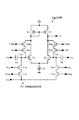
図19は、AD変換回路23の内部の基準電圧Vouti,Vrefiを調整する機能を備えた、実施例3に係る比較器の構成例を示す回路図であり、図中、図11と同等部位には同一符号を付して示している。
(Example 3)
FIG. 19 is a circuit diagram showing a configuration example of a comparator according to the third embodiment having a function of adjusting the reference voltages V outi and V refi inside the
図19に示すように、実施例3に係る比較器31Cは、前段の回路部と後段回路部との2段回路構成となっており、前段の回路部は、実施例1に係る比較器31Aと同じ回路構成、即ち、比較回路部81となっている。尚、前段の回路部については、実施例1に係る比較器31Aと同じ回路構成のものに限られるものではなく、実施例2に係る比較器31Bと同じ回路構成とすることも可能である。 As illustrated in FIG. 19, the comparator 31 C according to the third embodiment has a two-stage circuit configuration including a front-stage circuit unit and a rear-stage circuit unit, and the front-stage circuit unit is a comparator according to the first embodiment. The circuit configuration is the same as 31 A , that is, the comparison circuit unit 81. Note that the circuit section of the previous stage is not limited to the same circuit configuration as that of the comparator 31 A according to the first embodiment, and may be the same circuit configuration as that of the comparator 31 B according to the second embodiment. is there.
一方、後段の回路部は、前段の比較回路部81の出力電圧、即ち、PMOSトランジスタ57に流れる電流に応じた電圧によって決まる電流値に基づく(対応する)電圧値(バイアス電圧値)を記憶する記憶回路部82である。この記憶回路部82は、例えば、PMOSトランジスタ821、NMOSトランジスタ822,823、及び、容量824によって構成されている。
On the other hand, the subsequent circuit section stores an output voltage of the preceding comparison circuit section 81, that is, a voltage value (bias voltage value) based on (corresponding to) a current value determined by a voltage corresponding to the current flowing through the
PMOSトランジスタ821は、前段の比較回路部81の出力端、即ち、MOSトランジスタ52,57のドレイン共通接続ノードにゲート電極が接続され、電源Vddにソース電極が接続されている。NMOSトランジスタ822は、PMOSトランジスタ821のドレイン電極にドレイン電極が接続され、ソース電極が接地されている。
In the
NMOSトランジスタ823は、PMOSトランジスタ821のドレイン電極にドレイン電極が接続され、NMOSトランジスタ822のゲート電極にソース電極が接続されている。容量824は、NMOSトランジスタ822のゲート電極に一端が接続され、他端が接地されている。そして、MOSトランジスタ821,822のドレイン共通接続ノードが本比較器31Cの出力端となり、当該ドレイン共通接続ノードから比較出力Vcoが導出される。
The
NMOSトランジスタ823のゲート電極には、制御信号ΦR2が印加される。この制御信号ΦR2は、例えば、図1に示すタイミング制御部18から与えられる。すなわち、タイミング制御部18は、実施例3に係る比較器31Cの後段の回路部、即ち、記憶回路部82を制御する制御部としての機能を持っている。
A control signal Φ R2 is applied to the gate electrode of the
・第1駆動例
次に、比較回路部81の後段に記憶回路部82を有する、実施例3に係る比較器31Cの第1駆動例について、図20のタイミング波形図を用いて説明する。図20には、制御信号xΦR、制御信号Φextlk、制御信号xΦR2、傾斜状波形の参照信号Vref、及び、信号電圧Voutの各タイミング波形を示している。
First Driving Example Next, a first driving example of the comparator 31 C according to the third embodiment having the memory circuit unit 82 in the subsequent stage of the comparison circuit unit 81 will be described with reference to the timing waveform diagram of FIG. FIG. 20 shows timing waveforms of the control signal xΦ R , the control signal Φ extlk , the control signal xΦ R2 , the reference signal V ref having a ramp waveform, and the signal voltage V out .
先ず、CDS駆動時は、前段の比較回路部81において、制御信号xΦRによる制御の下に、PMOSトランジスタ58,59が導通することによって設定される初期電圧が、内部の基準電圧Vouti,VrefiとしてNMOSトランジスタ51,52のゲート側に保持される。この初期設定状態において、制御信号xΦR2による制御の下に、後段の記憶回路部82のNMOSトランジスタ83が導通状態となる。
First, when CDS driving, in front of the comparing circuit 81, a control signal Xfai R under the control of, the initial voltage set by the
後段の記憶回路部82において、NMOSトランジスタ83が導通状態となることで、前段の比較回路部81の初期設定値によって決まる出力電圧に応じた電流がMOSトランジスタ821,823を通して容量824に流れる。そして、初期設定期間内において、制御信号xΦR2による制御の下に、NMOSトランジスタ83が非導通状態になるタイミングで、比較回路部81の出力電圧の初期値によって決まる電流値に基づく電圧値が容量824に記憶(保持)される。
In the memory circuit unit 82 at the subsequent stage, the NMOS transistor 83 is turned on, so that a current corresponding to the output voltage determined by the initial setting value of the comparison circuit unit 81 at the previous stage flows to the
この容量824に記憶された電流値で後段の記憶回路部82の特性が決定される。後段の記憶回路部82の出力が反転するのは、比較回路部81の出力電流、即ち、PMOSトランジスタ821に流れる電流が容量824の保持電圧により発生する電流値を上回ったときとなる。
The characteristics of the subsequent storage circuit unit 82 are determined by the current value stored in the
一方、DDS駆動時は、前段の比較回路部81において、制御信号Φextによる制御の下に、NMOSトランジスタ71,72が導通状態になることで、外部設定初期電圧VextがNMOSトランジスタ51,52のゲート電極に与えられる。また、制御信号xΦR2による制御の下に、後段の記憶回路部82のNMOSトランジスタ83が導通状態となる。
On the other hand, at the time of DDS driving, the external setting initial voltage V ext becomes the
後段の記憶回路部82において、NMOSトランジスタ83が導通状態となることで、外部設定初期電圧Vextにより入力が決定されたときの出力電圧に応じた電流がMOSトランジスタ81,83を通して容量824に流れる。そして、制御信号xΦR2による制御の下に、NMOSトランジスタ83が非導通状態になるタイミングで、外部設定初期電圧Vextによって決まる電流値に基づく電圧値が容量824に記憶(保持)される。
In the memory circuit portion 82 at the subsequent stage, the NMOS transistor 83 becomes conductive, so that a current corresponding to the output voltage when the input is determined by the externally set initial voltage V ext flows to the
上述したように、第1駆動例の場合は、CDS駆動時、DDS駆動時共に、初期設定のときの比較回路部81の出力電圧によって決まる電流値に基づく電圧値を記憶回路部82で記憶するようにしている。しかしながら、上述した動作説明から明らかなように、比較回路部81のCDS駆動時における初期設定の出力電圧と、比較回路部81のDDS駆動時における初期設定の出力電圧とに差が生じる。 As described above, in the case of the first driving example, the voltage value based on the current value determined by the output voltage of the comparison circuit unit 81 at the initial setting is stored in the memory circuit unit 82 in both the CDS driving and the DDS driving. I am doing so. However, as is apparent from the above description of the operation, there is a difference between the initial setting output voltage when the comparison circuit unit 81 is driven by CDS and the initial setting output voltage when the comparison circuit unit 81 is DDS driving.
このように、CDS駆動時とDDS駆動時の初期設定の出力電圧に差が生じると、結果として、記憶回路部82が記憶する電圧値、即ち、記憶回路部82の出力が反転する電圧値がCDS駆動時とDDS駆動時で違ってくるため、比較器31Cとして同じ動作点が得られなくなる。すなわち、CDS駆動時とDDS駆動時で比較器31Cの初期の動作点が変わってしまう。この点に鑑みて為されたのが、以下に説明する第2駆動例である。 As described above, when a difference occurs in the output voltage of the initial setting during the CDS driving and the DDS driving, as a result, the voltage value stored in the memory circuit unit 82, that is, the voltage value at which the output of the memory circuit unit 82 is inverted is obtained. Since the CDS driving and the DDS driving are different, the same operating point as the comparator 31 C cannot be obtained. That is, the initial operating point of the comparator 31 C changes between CDS driving and DDS driving. In view of this point, the second driving example described below has been made.
・第2駆動例
続いて、実施例3に係る比較器31Cの第2駆動例について、図21のタイミング波形図を用いて説明する。図21にも、図20と同様に、制御信号xΦR、制御信号Φextlk、制御信号xΦR2、傾斜状波形の参照信号Vref、及び、信号電圧Voutの各タイミング波形を示している。
Second Driving Example Next, a second driving example of the comparator 31 C according to the third embodiment will be described with reference to the timing waveform diagram of FIG. FIG. 21 also shows timing waveforms of the control signal xΦ R , the control signal Φ extlk , the control signal xΦ R2 , the reference signal V ref having a ramp waveform, and the signal voltage V out , as in FIG.
第2駆動例の場合、CDS駆動時の動作については第1駆動例の場合と同じであり、DDS駆動時の動作を特徴としている。すなわち、図20のタイミング波形図と図21のタイミング波形図との対比から明らかなように、DDS駆動の際に、制御信号Φextによる制御に基づく外部設定初期電圧Vextによる初期設定を行う前に、CDS駆動時と同じ初期設定の動作を行う構成を採っている。 In the case of the second driving example, the operation at the time of CDS driving is the same as that in the case of the first driving example and is characterized by the operation at the time of DDS driving. That is, as apparent from the comparison between the timing waveform diagram of FIG. 20 and the timing waveform diagram of FIG. 21, before performing the initial setting by the externally set initial voltage V ext based on the control by the control signal Φ ext at the time of DDS driving. Further, the same initial setting operation as that at the time of CDS driving is employed.
具体的には、外部設定初期電圧Vextによる初期設定に先立って、前段の比較回路部81において、制御信号xΦRによる制御の下に、PMOSトランジスタ58,59が導通することによって設定される初期電圧を、内部の基準電圧Vouti,Vrefiとして初期設定する。
Initial Specifically, prior to the initial setting by the externally set initial voltage V ext, in front of the comparing circuit 81, which under the control of the control signal Xfai R, is set by the
この初期設定状態において、制御信号xΦR2による制御の下に、後段の記憶回路部82において、NMOSトランジスタ823が非導通状態になるタイミングで、比較回路部81の出力電圧の初期値によって決まる電流値に基づく電圧値を容量824に記憶(保持)する。このとき記憶する電圧値(電流値)は、CDS駆動時の初期設定で記憶する電圧値(電流値)と同じである。これにより、CDS駆動時とDDS駆動時で比較器31Cの初期の動作点、即ち、両者の特性が揃うことになる。
In this initial setting state, under the control of the control signal xΦ R2, the current value determined by the initial value of the output voltage of the comparison circuit unit 81 at the timing when the
DDS駆動の際には、CDS駆動時と同じ初期設定を行った後、再度、外部設定初期電圧Vextによる初期設定を行うことで、信号レベルVsig及びリセットレベルVrstがAD変換回路23の入力電圧範囲内に入るように内部の基準電圧Vouti,Vrefiを調整する。
In the DDS driving, the same initial setting as in the CDS driving is performed, and then the initial setting by the external setting initial voltage V ext is performed again, so that the signal level V sig and the reset level V rst are changed in the
上述したように、DDS駆動の際には、外部設定初期電圧Vextによる初期設定に先立って、CDS駆動時と同じ初期設定を行い、しかる後再度本来の初期設定、即ち、外部設定初期電圧Vextによる初期設定を行うことで、第1駆動例の問題を解決することができる。すなわち、DDS駆動、CDS駆動の双方において、同じ初期設定を行うことにより両駆動時の出力の動作点の特性を揃えることができる。その結果、初期電圧設定回路70Aの作用による作用、効果に加えて、CDS駆動とDDS駆動とをより確実に両立できる、という作用、効果を得ることができる。 As described above, at the time of DDS driving, the same initial setting as that at the time of CDS driving is performed prior to the initial setting by the external setting initial voltage V ext , and then the original initial setting, that is, the external setting initial voltage V By performing the initial setting with ext , the problem of the first driving example can be solved. In other words, by performing the same initial setting in both the DDS drive and the CDS drive, it is possible to align the characteristics of the operating points of the outputs during both drives. As a result, in addition to the operation and effect of the operation of the initial voltage setting circuit 70 A , the operation and effect that both the CDS drive and the DDS drive can be achieved more reliably can be obtained.
(駆動の高速化)
ところで、本実施形態に係るCMOSイメージセンサ10Aにおいては、単純に、CDS駆動とDDS駆動を交互に行うことで信号を取得する訳であるが、当然のことながら、信号の取得にはCDS駆動及びDDS駆動の時間分の時間を要することになる。具体的には、図22のタイミング波形図に示すように、DDS駆動の駆動時間をTdds、CDS駆動の駆動時間をTcdsとすると、CDS駆動及びDDS駆動で信号を取得する時間Ttotalは、Ttotal=Tdds+Tcdsとなる。この駆動例の場合は、AD変換の際に用いる傾斜状波形の参照信号Vrefのスロープ(傾斜)について、CDS駆動とDDS駆動で同じ勾配Aとなっている。
(Speeding up the drive)
By the way, in the CMOS image sensor 10 A according to the present embodiment, the signal is simply obtained by alternately performing the CDS driving and the DDS driving. In addition, a time corresponding to the DDS driving time is required. Specifically, as shown in the timing waveform diagram of FIG. 22, assuming that the drive time for DDS drive is T dds and the drive time for CDS drive is T cds , the time T total for acquiring signals by CDS drive and DDS drive is , T total = T dds + T cds . In the case of this driving example, the slope (inclination) of the reference signal Vref having an inclined waveform used for AD conversion has the same gradient A in the CDS driving and the DDS driving.
これに対して、傾斜状波形の参照信号Vrefに関して、CDS駆動及びDDS駆動のどちらか一方のスロープを他方のスロープに比べて急勾配にすることにより、AD変換に要する時間、ひいては、信号を取得するまでの時間を高速化できる。スロープを急勾配にした方の駆動によって得られるデータについては、後段の信号処理部において、高速化した分だけ、即ち、参照信号Vrefのスロープを急勾配にした分だけ係数(後述する)をかけることにより、入力換算で同じデータを取得するようにすれば良い。 On the other hand, with respect to the reference signal V ref having a sloped waveform, the time required for AD conversion, that is, the signal is changed by making the slope of one of the CDS drive and the DDS drive steeper than the other slope. The time to obtain can be increased. For the data obtained by driving the slope with a steep slope, the coefficient (described later) is increased in the signal processing unit at the subsequent stage by the speed increase, that is, the slope of the reference signal V ref is steep. By doing so, the same data may be acquired by input conversion.
一般的に、DDS駆動で取得する信号については、イメージセンサでは高輝度側の信号であることが多いために、DDS駆動側について、参照信号VrefのスロープをCDS駆動側に比べて急勾配にするのが望ましい。 In general, since signals acquired by DDS driving are often high-luminance signals in image sensors, the slope of the reference signal V ref is steeper on the DDS driving side than on the CDS driving side. It is desirable to do.
図23に、参照信号VrefのスロープについてDDS駆動側をCDS駆動側(勾配A)に比べて急勾配A′にした場合のタイミング波形を示す。DDS駆動側を急勾配A′にすることで、AD変換に要する時間は、Tdds´+Tcdsとなる。ここで、Tdds´=Tdds−(t1−t1´)−(t2−t2´)の時間の短縮が見込まれる。そして、その短縮分だけ信号を取得するまでの時間を高速化できる。 FIG. 23 shows timing waveforms when the slope of the reference signal V ref is a steep slope A ′ on the DDS driving side compared to the CDS driving side (gradient A). By setting the DDS driving side to the steep slope A ′, the time required for AD conversion becomes T dds ′ + T cds . Here, T dds ′ = T dds − (t 1 −t 1 ′) − (t 2 −t 2 ′) is expected to be shortened. And it is possible to speed up the time until the signal is acquired by the shortened amount.
高速化を図る図22の場合のDDS駆動時のスロープの傾き(勾配)をAとし、高速化を図った場合のDDS駆動時のスロープの傾きをA´としたとき、後段の信号処理部において用いる、先述した係数は、A´/Aとなる。すなわち、高速化した場合のDDS駆動で得られたデータに対してA´/Aなる係数をかけることで、高速化していない場合と同等の出力データを得ることが可能になる。尚、この係数をかける信号処理は、画素アレイ部12と同じチップ(半導体基板19)内、チップ外のどちらで行っても良く、特に制約は無い。
In the case of FIG. 22 for increasing the speed, the slope (gradient) of the slope during DDS driving is A, and the slope of the slope during DDS driving when increasing the speed is A ′. The aforementioned coefficient used is A ′ / A. That is, by applying a coefficient A ′ / A to the data obtained by DDS driving when the speed is increased, it is possible to obtain output data equivalent to the case where the speed is not increased. The signal processing for applying this coefficient may be performed either on the same chip (semiconductor substrate 19) as the
また、画素アレイ部12の全画素11に亘ってDDS駆動で取得する信号が無く、DDS動作自体が不要な信号レベルの場合、例えば、非常に暗い環境下での撮像の場合は、DDS駆動を止めてCDS駆動のみとすることによっても動作速度を向上させることができる。この場合、一例として、DDS駆動での出力データがゼロ出力と判定可能な出力結果がある一定時間連続していることを検出したら、その検出結果を受けてCDS駆動のみとする、といった制御が考えられる。
In addition, when there is no signal acquired by DDS driving over all the
(カウンタの駆動法)
前にも述べたことから明らかなように、傾斜状波形の参照信号Vrefを用いる、所謂、スロープ型のAD変換回路23は、単調減少(または、単調増加)する傾斜状波形の参照信号Vrefと画素の信号電圧Voutとを比較する。そして、比較器31の出力が反転するまでの時間をクロックCKによってカウントし、比較器31の出力の反転タイミングでのカウント値を変換データとして記憶することでAD変換を実現している。
(Counter driving method)
As is apparent from the above, the so-called slope-type
先述した実施形態の説明では、カラムAD変換回路のカウント部としてアップ/ダウンカウンタ32を用いるとしたが、例えば、カウント部が正負12ビットカウント可能な場合、CDS駆動ではダウンカウントのカウンタを搭載するものとする。図24に、CDS駆動時のカウンタ部の動作説明に供するタイミング波形を示す。CDS駆動では、リセットレベルVRSTまでの反転時刻tをダウンカウントし、カウント終了後1の補数を取ることで0を中心に正負を逆−1とした値にする。
In the description of the above-described embodiment, the up / down
次に、信号レベルVsigについてもこの値を基準にダウンカウントを行う。もし、単位画素11の信号が低照度(DARK)で同じ電位レベルしか比較器31に入力されないと仮定すると、図25に示すように、カウント値−1でカウントが終了する。単位画素11の信号が高照度であった場合は、図26に示すように、−4096までカウントする。最後に、このデータの1の補数を取得することで、低照度時は0、高照度時は4095のデータを出力できることとなる。
Next, the signal level V sig is also counted down based on this value. If it is assumed that the signal of the
しかしながら、同じ回路(カウンタ)を使用してDDS駆動のデータを取得しようとすると、高照度側では、わずかのカウント後に比較器31の出力が反転するため、CDS駆動時の低照度と同じレベルの信号が出力される。すなわち、DDS駆動の高照度時はCDS駆動の低照度に近いタイミングで反転し、DDS駆動の低照度時はCDS駆動の高照度時に近いタイミングで反転するために、同じ回路(カウンタ)を用いての入力信号とデータの整合性が取れないことになる。 However, if DDS drive data is acquired using the same circuit (counter), the output of the comparator 31 is inverted after a slight count on the high illuminance side. A signal is output. That is, the same circuit (counter) is used to invert at the timing close to the low illuminance of the CDS drive at the high illuminance of the DDS drive, and to reverse at the timing close to the high illuminance of the CDS drive at the low illuminance of the DDS drive. Therefore, the consistency of the input signal and the data cannot be obtained.
図27は、DDS駆動時のカウンタ部の動作説明に供するタイミング波形図である。また、図28には、DDS駆動の低照度時のカウント動作についての説明図を示し、図29には、DDS駆動の高照度時のカウント動作についての説明図を示す。 FIG. 27 is a timing waveform chart for explaining the operation of the counter unit during DDS driving. FIG. 28 is an explanatory diagram for the counting operation at low illuminance in DDS driving, and FIG. 29 is an explanatory diagram for the counting operation at high illuminance in DDS driving.
カラムAD変換回路のカウント部において、同じ回路(カウンタ)を用いての入力信号とデータの整合性を取るために、DDS駆動では、以下のような駆動を行うようにする。すなわち、DDS駆動で取得した信号については、例えば列走査部16による走査で選択した後、外部に出力する前に4096のデータを加算して出力するようにする。
In the count section of the column AD converter circuit, in order to ensure consistency between the input signal and data using the same circuit (counter), the following drive is performed in the DDS drive. That is, for the signal acquired by DDS driving, for example, after being selected by scanning by the
4096のデータの加算処理については、画素アレイ部12と同じチップ(半導体基板19)内で行っても良いし、チップ外部で演算処理の一環として行うようにしても良い。この加算処理回路については、DDS駆動で取得した信号であるか否かを判別する回路部と、当該回路部の判別結果を受けてDDS駆動時に加算処理を行う加算器とによって実現することが可能である。
The addition process of 4096 data may be performed within the same chip (semiconductor substrate 19) as the
このように、DDS駆動では、DDS駆動で取得した信号に対して、カウンタのビット数に対応したデータ、例えば12ビットの場合には4096のデータを加算することで、同じ回路(カウンタ)を用いての入力信号とデータの整合性を取ることができる。すなわち、CDS駆動とDDS駆動のデータの取得の際に、カラムAD変換回路のカウント部として同一の回路(カウンタ)を使用することが可能となる。 In this way, in DDS driving, the same circuit (counter) is used by adding data corresponding to the number of bits of the counter, for example, 4096 data in the case of 12 bits, to the signal acquired by DDS driving. All input signals and data can be consistent. In other words, the same circuit (counter) can be used as the counting unit of the column AD conversion circuit when acquiring data for CDS driving and DDS driving.
<2.第2実施形態>
[2−1.システム構成]
図30は、本開示の第2実施形態に係るCMOSイメージセンサの構成の概略を示すシステム構成図であり、図中、図1と同等部位には同一符号を付して示している。
<2. Second Embodiment>
[2-1. System configuration]
FIG. 30 is a system configuration diagram illustrating an outline of the configuration of a CMOS image sensor according to the second embodiment of the present disclosure. In FIG. 30, the same components as those in FIG. 1 are denoted by the same reference numerals.
図30に示すように、本実施形態に係るCMOSイメージセンサ10Bは、画素アレイ部12に加えて、その周辺回路として、例えば、行走査部13、カラム処理部14B、参照信号生成部15、列走査部16、水平出力線17、及び、タイミング制御部18を有する。
As shown in FIG. 30, the CMOS image sensor 10 B according to the present embodiment includes, for example, a
CMOSイメージセンサ10Bにおいては、カラム処理部14Bが第1実施形態のカラム処理部14Aと構成を異にしているだけであり、行走査部13、参照信号生成部15、列走査部16、水平出力線17、及び、タイミング制御部18については、基本的に、第1実施形態と同じである。
In the CMOS image sensor 10 B , the column processing unit 14 B only differs from the column processing unit 14 A of the first embodiment in configuration, and the
カラム処理部14Bは、例えば、画素アレイ部12の画素列毎、即ち、列信号線22(22-1〜22-m)毎に1対1の対応関係をもって設けられたカラムアンプ回路25(25-1〜25-m)を有する。カラムアンプ回路25(25-1〜25-m)は、画素アレイ部12の各単位画素11から列毎に出力されるアナログ信号に対して増幅処理を行うとともに、信号レベルとリセットレベルとの差分をとる相関二重サンプリング処理を行う。
Column processing section 14 B, for example, each pixel column of the
カラムアンプ回路25-1〜25-mは全て同じ構成となっている。ここでは、m列目のカラムアンプ回路25-mを例に挙げて説明するものとする。カラムアンプ回路25-mは、反転増幅器61、入力容量62、帰還容量63、制御スイッチ64、及び、水平選択スイッチ65を有する構成となっている。そして、カラムアンプ回路25-mは、列信号線22-mを介して単位画素11から供給される信号電圧Voutを増幅してアナログ信号Vampとして出力する。
The
尚、本例では、カラム処理部14Bについて、カラムアンプ回路25が列信号線22毎に1対1の対応関係をもって設けられた構成を例に挙げたが、1対1の対応関係の配置に限られるものではない。例えば、1つのカラムアンプ回路25を複数の画素列で共有し、複数の画素列間で時分割にて使用する構成とすることも可能である。
In this example, the column processing unit 14 B has a configuration in which the
(カラムアンプ回路の従来構成について)
信号処理部として、列並列に配置されたカラムアンプ回路25を用いる従来のCMOSイメージセンサは、CDS駆動を基本としている。すなわち、単位画素11から先にリセットレベルVrstを読み出し、次いで、信号レベルVsigが読み出すCDS駆動を基本としている。ここで、この従来例に係るCMOSイメージセンサに用いられるカラムアンプ回路の構成例について説明する
(Conventional configuration of column amplifier circuit)
A conventional CMOS image sensor using a
図31は、カラムアンプ回路25の従来構成を示す回路図である。図32に、従来構成に係るカラムアンプ回路25の出力信号の動作範囲を示す。
FIG. 31 is a circuit diagram showing a conventional configuration of the
図31に示すように、従来構成に係るカラムアンプ回路25は、反転増幅器61、入力容量62、帰還容量63、及び、制御スイッチ64を有する構成となっている。このカラムアンプ回路25においても、AD変換回路23の場合と同様に、制御信号ΦRによる制御の下に、制御スイッチ64によって反転増幅器61の入出力端間を短絡することで、カラムアンプ回路25の基準電圧を取得する。
As shown in FIG. 31, the
CDS動作では、リセットレベルVrst→信号レベルVsigの順に読み出されるが、電位的には、高い電位→低い電位となる。カラムアンプ回路25において、初期値として、出力電圧は低く設定し、入力信号が低くなる場合、即ち、単位画素11からの信号レベルが大きくなる場合、低い初期出力電圧が入力容量62と帰還容量63の容量比で増幅される。具体的には、入力容量62の容量値をCin、帰還容量63の容量値をCfbとすると、容量比Cin/Cfbで増幅される。
In the CDS operation, reading is performed in the order of the reset level V rst → the signal level V sig , but the potential is changed from a high potential to a low potential. In the
制御信号ΦRによる制御の下に、制御スイッチ64によって反転増幅器61の入出力端間を短絡したときの初期電圧(基準電圧)をVbとすると、カラムアンプ回路25の出力電圧Vampは、
Vamp=Vb+(Cin/Cfb)ΔV
となる。ここで、ΔVはリセットレベルVrstと信号レベルVsigの電位差である。カラムアンプ回路25の出力動作範囲は、反転増幅器61の入出力端間を短絡したときの初期電圧Vbに対して閾値電圧程度低い電圧から、カラムアンプ回路25の回路構成で決まる上部の動作範囲までとなる。
If the initial voltage (reference voltage) when the input / output terminals of the inverting amplifier 61 are short-circuited by the
V amp = V b + (C in / C fb ) ΔV
It becomes. Here, ΔV is a potential difference between the reset level V rst and the signal level V sig . The output operation range of the
この従来構成に係るカラムアンプ回路25を用いたCMOSイメージセンサでDDS駆動を行った場合の、カラムアンプ回路25の出力波形を図33に示す。
FIG. 33 shows an output waveform of the
DDS駆動では、信号出力順がCDS駆動の場合と逆である、即ち、信号レベルVsig→リセットレベルVrstの順に出力される。従って、カラムアンプ回路25の出力信号は、低い初期電圧の電圧値から更に低くなるため、回路の動作範囲を外れてしまう。これを解決するために、第2実施形態では以下の構成を採っている。
In the DDS drive, the signal output order is reverse to that in the CDS drive, that is, the signal level V sig is output in the order of the reset level V rst . Accordingly, the output signal of the
[2−2.第2実施形態の特徴とする事項]
すなわち、第2実施形態では、単位画素11からのアナログ信号に対して増幅処理を行うとともに、信号レベルVsigとリセットレベルVrstとの差分をとる相関二重サンプリング処理を行うカラムアンプ回路25を用いたCMOSイメージセンサ10Bにおいて、次の構成を採ることを特徴とする。
[2-2. Matters Characteristic of Second Embodiment]
That is, in the second embodiment, the
具体的には、先ず、単位画素11の信号を第1の信号及び第2の信号として2回に分けて読み出す際に、先に読み出される第1の信号を、第1,第2の信号を処理する信号処理部の処理可能な入力電圧範囲の基準電圧として用いる。本実施形態の場合は、カラムアンプ回路25が、第1,第2の信号を処理する信号処理部に相当する。また、基準電圧は、カラムアンプ回路25の増幅可能な入力電圧範囲の基準となる電圧となる。
Specifically, first, when the signal of the
このとき、第1の信号がFD部42に蓄積、もしくは、保持された信号電荷に基づく信号、即ち、信号レベルVsigである場合は、当該信号レベルを基準電圧として用いることになる。また、第1の信号がFD部42をリセットしたときのリセット電位Vrに基づく信号、即ち、リセットレベルVrstである場合は、当該リセットレベルを基準電圧として用いることになる。そして、先に読み出される第1の信号をカラムアンプ回路25の基準電圧として用いた上で、第1,第2の信号がカラムアンプ回路25の入力電圧範囲内に入るように基準電圧を調整した状態で第1,第2の信号に対して増幅処理を施すようにする。
At this time, when the first signal is a signal based on the signal charge accumulated or held in the
このように、第1,第2の信号がカラムアンプ回路25の入力電圧範囲内に入るように基準電圧を調整することで、カラムアンプ回路25は、第1,第2の信号が入力電圧範囲内に入った状態でこれら第1,第2の信号に対して増幅処理を施すことが可能になる。従って、先に読み出される第1の信号が信号レベルVsigの場合、リセットレベルVrstの場合のいずれの場合にも、処理対象の画素の信号を用いて基準電圧を設定した上で、第1,第2の信号に対して確実に信号増幅処理を施すことができることとなる。
Thus, by adjusting the reference voltage so that the first and second signals fall within the input voltage range of the
これにより、特許文献5に記載の従来技術、即ち、別途外部で生成した所定電圧を用いて基準電圧を設定する場合のような、面内の大きな特性の揺らぎの差異や、寄生容量の大きさに依存したオフセット成分を効果的に除去できる。その結果、画素の出力振幅に対して、カラムアンプ回路25の増幅可能な入力電圧範囲に必要なマージンを低減することが可能となる。そして、当該入力電圧範囲に必要なマージンを低減できることにより、カラムアンプ回路25の電源電圧の低電圧化や低消費電力化を図ることができる。
As a result, the conventional technique described in Patent Document 5, that is, the case where the reference voltage is set by using a predetermined voltage generated separately outside, a large difference in fluctuation of characteristics in the surface, and the size of the parasitic capacitance. The offset component depending on can be effectively removed. As a result, it is possible to reduce a margin necessary for the input voltage range that can be amplified by the
(実施例1)
以下に、具体的な実施例について説明する。前にも述べたように、DDS駆動では、先ず、FD部42に保持、もしくは、蓄積されている信号電荷を信号レベルVsigとして読み出す駆動が行われる。次いで、FD部42をリセット電位Vrにリセットして当該リセット電位VrをリセットレベルVrstとして読み出す駆動が行われる。そして、単位画素11から先に読み出される信号レベルVsigを、カラムアンプ回路25の変換可能な入力電圧範囲の基準となる基準電圧として用いる。換言すれば、先に読み出される信号レベルVsigを用いてカラムアンプ回路25の基準電圧を設定する。
Example 1
Specific examples will be described below. As described above, in the DDS drive, first, a drive for reading the signal charge held or accumulated in the
図34は、基準電圧を調整する機能を備えた、実施例1に係るカラムアンプ回路についての説明図であり、(A)はカラムアンプ回路の構成例を、(B)はカラムアンプ回路の動作範囲をそれぞれ示している。図34において、図31と同等部位には同一符号を付して示している。 FIG. 34 is an explanatory diagram of the column amplifier circuit according to the first embodiment having a function of adjusting the reference voltage, where (A) is a configuration example of the column amplifier circuit, and (B) is an operation of the column amplifier circuit. Each range is shown. 34, parts equivalent to those in FIG. 31 are denoted by the same reference numerals.
図34(A)に示すように、実施例1に係るカラムアンプ回路25Aは、反転増幅器61、入力容量62、帰還容量63、及び、制御スイッチ64に加えて、カラムアンプ回路25Aの基準電圧を設定(調整)するための初期電圧設定回路70Bを有する構成となっている。
As shown in FIG. 34 (A),
初期電圧設定回路70Bは、帰還容量63に対して直列に接続されたNMOSトランジスタ75と、帰還容量63とNMOSトランジスタ75との接続ノードと外部設定初期電圧Vextが与えられるラインLとの間に接続されたPMOSトランジスタ76によって構成されている。NMOSトランジスタ75及びPMOSトランジスタ76の各ゲート電極には、制御信号Φextの反転信号xΦextが印加される。制御信号Φextの反転信号xΦextは、例えば、図1に示すタイミング制御部18から与えられる。すなわち、タイミング制御部18は、初期電圧設定回路70Bを制御する制御部としての機能を持っている。
The initial voltage setting circuit 70 B includes an
図35は、実施例1に係るカラムアンプ回路25Aの各部位の信号波形を示す波形図である。図35には、制御信号Φextの反転信号xΦext、制御信号ΦR、列信号線22の信号電圧Vout、即ちカラムアンプ回路25Aの入力電圧、及び、カラムアンプ回路25Aの出力電圧Vampの各波形を示している。
FIG. 35 is a waveform diagram illustrating signal waveforms of respective parts of the
CDS駆動の場合は、制御信号Φextの反転信号xΦextが高電位の状態にあることで、NMOSトランジスタ75が導通状態になり、帰還容量63をカラムアンプ回路25Aの出力端に電気的に接続する。このときの回路構成は、図31に示したカラムアンプ回路25と同じ回路構成、即ち、通常のCDS駆動時の同じ回路形態となる。
For CDS driving, by inverting the signal Xfai ext of the control signal [Phi ext is in the state of high potential, the
DDS駆動時は、カラムアンプ回路25A自体の入出力間を短絡することで、カラムアンプ回路25Aの入力信号は初期電圧(基準電圧)をVbとなる。これにより、出力振幅を確保でき、かつ、回路の動作する入力信号レベルとなる。
When DDS drive, by short-circuiting the input and output of the
一方で、制御信号Φextの反転信号xΦextが低電位の状態になることで、NMOSトランジスタ75が非導通状態となり、カラムアンプ回路25Aの出力端に対する帰還容量63の電気的接続を開放する。すなわち、反転増幅器61の帰還ループを開放状態にする。このとき、PMOSトランジスタ76が導通状態になり、帰還容量63の開放端に対して外部設定初期電圧Vextを印加する。これにより、反転増幅器61の出力電圧の初期値は、外部設定初期電圧Vextとなる。そして、DDS駆動の場合は、入力信号は、低い信号レベルから高いリセットレベルへと変化するので、この動作範囲になるように、カラムアンプ回路25Aの基準電圧の調整が行われる。
On the other hand, when the inverted signal xΦ ext of the control signal Φ ext becomes a low potential state, the
このように、DDS駆動時において、初期電圧設定回路70Bの作用により、信号レベルVsig及びリセットレベルVrstがカラムアンプ回路25Aの動作範囲内に入るように基準電圧を調整することで、CDS駆動とDDS駆動の両立が可能になる。
In this way, by adjusting the reference voltage so that the signal level V sig and the reset level V rst fall within the operation range of the
また、基準電圧を調整するための初期電圧設定回路70Bとしては、2つのMOSトランジスタ75,76を追加するだけの非常に簡単な回路構成で実現できる。従って、個々のカラムアンプ回路25Aとしては、僅かな面積の増加で済む。すなわち、CDS駆動とDDS駆動との両立を、カラムアンプ回路25Aの面積を僅かに増加するだけで実現できる。
Further, the initial voltage setting circuit 70 B for adjusting the reference voltage can be realized with a very simple circuit configuration in which only two
(実施例2)
図36は、基準電圧を調整する機能を備えた、実施例2に係るカラムアンプ回路の構成例を示す回路図であり、図中、図34と同等部位には同一符号を付して示している。
(Example 2)
FIG. 36 is a circuit diagram illustrating a configuration example of the column amplifier circuit according to the second embodiment having a function of adjusting the reference voltage. In FIG. 36, the same components as those in FIG. 34 are denoted by the same reference numerals. Yes.
実施例2に係るカラムアンプ回路25Bは、入力側の容量と出力側の容量の容量比で信号を増幅する構成となっている。具体的には、反転増幅器61の出力端に、スイッチSW11〜SW14を介して4つの出力容量CN1,CS1,CN2,CS2が接続され、これら出力容量CN1,CS1,CN2,CS2の保持電荷がスイッチSW21〜SW24によって選択的に出力される構成となっている。出力側の容量の回路部分以外の構成、及び、その動作については、実施例1に係るカラムアンプ回路25Aの場合と同じである。
The
また、反転増幅器61の帰還容量63の部位には、実施例1に係るカラムアンプ回路25Aの場合と同様に、カラムアンプ回路25Bの基準電圧を設定(調整)するための初期電圧設定回路70Bが設けられている。初期電圧設定回路70Bは、実施例1の同様の構成、即ち、帰還容量63に対して直列に接続されたNMOSトランジスタ75と、帰還容量63とNMOSトランジスタ75との接続ノードに外部設定初期電圧Vextを選択的に与えるPMOSトランジスタ76とを有する構成となっている。
An initial voltage setting circuit for setting (adjusting) the reference voltage of the
次に、上記構成の実施例2に係るカラムアンプ回路25Bの回路動作について、図37のタイミング波形図を用いて説明する。
Next, the circuit operation of the
第1実施形態の場合と同様、DDS駆動時にカラムアンプ回路25Bの出力が下側に飽和しないように、初期電圧として外部設定初期電圧Vextを設定する。その設定後、フィードバックがかかった状態のカラムアンプ回路25Bの出力信号を制御信号ΦS1にて出力容量CS1にサンプルする。続いて、単位画素11のリセット信号RSTをアクティブ状態にして、信号レベルを制御信号ΦN1にて出力容量CN1にサンプルする。
As in the case of the first embodiment, the externally set initial voltage V ext is set as the initial voltage so that the output of the
カラムアンプ回路25Bに対して制御信号(リセット信号)ΦRを入力し、同時に、単位画素11のFD部42をリセットする。これにより、カラムアンプ回路25Bの入力側は初期電圧Vbに設定される。制御信号ΦRの印加をやめた状態を初期値として出力容量CN2に制御信号ΦN2にてサンプルし、転送信号TRGにてフォトダイオード41からFD部42へ信号を転送した後に制御信号ΦS2にて出力容量CS2にサンプルする。出力容量CN1,CS1には、DDS駆動での信号レベル差、出力容量CN2,CS2にはCDS駆動での信号レベル差が蓄積されている。これらの信号を水平転送制御で出力へ読み出す。
A control signal (reset signal) Φ R is input to the
このように、入力側の容量と出力側の容量の容量比で信号を増幅する構成のカラムアンプ回路25Bにおいても、初期電圧設定回路70Bの作用により、適切な初期状態とすることで、CDS駆動とDDS駆動とで、同一回路を用いて動作範囲内に出力が収まるように動作させることが可能となる。
In this way, even in the
また、基準電圧を調整するための初期電圧設定回路70Bとしては、2つのMOSトランジスタ75,76を追加するだけの非常に簡単な回路構成で実現できる。従って、個々のカラムアンプ回路25Bとしては、僅かな面積の増加で済む。すなわち、CDS駆動とDDS駆動との両立を、カラムアンプ回路25Bの面積を僅かに増加するだけで実現できる。
Further, the initial voltage setting circuit 70 B for adjusting the reference voltage can be realized with a very simple circuit configuration in which only two
また、DDS駆動とCDS駆動とでカラムアンプ回路25Bの入力側と帰還側の容量比を変えることで、信号のゲインをおのおの個別に設定可能となる。加えて、カラムアンプ回路25Bの出力側に、第1実施形態に係るシングルスロープ型のAD変換回路を接続し、制御信号ΦN1,ΦN2,ΦS1,ΦS2で表された期間にAD変換を行うことで、信号を取得することも可能となる。
Further, by changing the capacitance ratio between the input side and the feedback side of the
<3.他の画素構成>
第1、第2実施形態においては、リセットレベルを信号レベルの前に読み出すことができない固体撮像装置として、グローバル露光機能を持つCMOSイメージセンサ10A,10Bを例に挙げた。このグローバル露光機能を持つCMOSイメージセンサ10A,10Bは、全画素一括の露光を実現すべく、フォトダイオード41で発生した電荷を全画素同時にFD部42へ転送し、当該FD部42で信号電荷が保持された状態から、順次読み出し動作を実行する。
<3. Other pixel configurations>
In the first and second embodiments, the CMOS image sensors 10 A and 10 B having the global exposure function are taken as an example as a solid-state imaging device that cannot read the reset level before the signal level. The CMOS image sensors 10 A and 10 B having the global exposure function transfer charges generated in the
但し、信号検出部にリセット前に読み出したい信号電荷が存在するため、リセットレベルを信号レベルの前に読み出すことができない固体撮像装置としては、グローバル露光機能を持つCMOSイメージセンサ10A,10Bに限られるものではない。以下に他の画素例について説明する。 However, since there is a signal charge to be read before resetting in the signal detection unit, as a solid-state imaging device in which the reset level cannot be read before the signal level, CMOS image sensors 10 A and 10 B having a global exposure function are used. It is not limited. Other pixel examples will be described below.
(他の画素例1)
図38は、有機光電変換膜を用いた、他の画素例1に係る単位画素の一例を示す構成図であり、図中、図2と同等部位には同一符号を付して示している。
(Other pixel example 1)
FIG. 38 is a configuration diagram illustrating an example of a unit pixel according to another pixel example 1 using an organic photoelectric conversion film. In FIG. 38, the same parts as those in FIG. 2 are denoted by the same reference numerals.
他の画素例1に係る単位画素11Aにおいて、有機光電変換膜81は上部電極82と下部電極83で挟まれている。少なくとも下部電極83は画素毎に分割され、透明性の高い電極が使われることが多い。そして、上部電極82に対してバイアス電源84によりバイアス電圧Vbが印加されている。
In the
有機光電変換膜81での光電変換によって発生した電荷はFD部42に蓄積される。FD部42の電荷は、増幅トランジスタ45を含む読み出し回路を介して列信号線22から電圧として読み出される。FD部26は、リセットトランジスタ44によりドレイン電位Vrに設定される。そして、リセットトランジスタ44のドレイン電位Vrは、FD部42の空乏化されたリセットトランジスタ44側のポテンシャルよりも低い電圧Vr1から高い電圧Vr2へ遷移させることが可能となっている。
Electric charges generated by photoelectric conversion in the organic photoelectric conversion film 81 are accumulated in the
このように、有機光電変換膜81を用いた、他の画素例1に係る単位画素11Aの場合は、DDS駆動によって該当画素の信号を読み出す。他の有機光電変換膜のついていない、もしくは、有機光電変換膜の機能が無効となっている、4つのトランジスタ等で構成されたCDS動作が可能な画素については、別の駆動によって信号を読み出す。例えば、有機光電変換膜81を用いていない他の画素が、例えば図2に示す画素構成の場合は、DDS駆動とCDS駆動の組み合わせ、もしくは、CDS駆動のみの読出しを行う。
Thus, using an organic photoelectric conversion film 81, in the case of the
この他の画素例1に係る単位画素11Aを用いた固体撮像装置に対しても、先述した第1,第2実施形態に係る信号処理部に関する技術を同様に適用することができる。すなわち、同一の信号処理部によってDDS駆動とCDS駆動を両立できる。
Even for the solid-state imaging device using the
(他の画素例2)
次に、単位画素内にFD部42以外に電荷蓄積部を有する画素について、他の画素例2として説明する。ここでは、FD部42以外に電荷蓄積部を有する画素構成として2つの例を図39(A),(B)に示す。図39(A),(B)において、図2と同等部位には同一符号を付して示している。
(Other pixel example 2)
Next, a pixel having a charge storage unit in addition to the
図39(A)に示す画素構成に係る単位画素11Bは、増幅トランジスタ45のゲート電極に対して、容量選択トランジスタ47を介して蓄積容量48が電荷蓄積部として接続された画素構成となっている。図39(B)に示す画素構成に係る単位画素11Cは、容量選択トランジスタ47が増幅トランジスタ45とリセットトランジスタ44との間に接続され、その接続ノードとグランドとの間に蓄積容量48が接続された画素構成となっている。
The
上記構成の他の画素例2に係る単位画素11B,11Cを用いた固体撮像装置に対しても、先述した第1,第2実施形態に係る信号処理部に関する技術を同様に適用することができる。すなわち、同一の信号処理部によってDDS駆動とCDS駆動を両立できる。
The technique related to the signal processing unit according to the first and second embodiments described above is similarly applied to the solid-state imaging device using the
ここで、一例として、CDS駆動→DDS駆動の順で画素から信号を読み出す場合の動作について、図40のタイミング波形図を用いて説明する。 Here, as an example, an operation in the case of reading a signal from a pixel in the order of CDS driving → DDS driving will be described with reference to a timing waveform diagram of FIG.
選択信号SELによって選択トランジスタ46を導通状態にした後、リセット信号RSTによってリセットトランジスタ44を導通状態にし、FD部42をリセットする。このとき。容量選択トランジスタ47については非導通状態にしておく。そして、リセットしたときのFD部42の電位をリセットレベルとして読み出し、次いで、転送信号TRGをアクティブ状態にすることによってフォトダイオード41からFD部42に信号電荷を読み出す。この一連の駆動がCDS駆動である。
After the
続いて、容量選択トランジスタ47を導通状態にし、FD部42と蓄積容量48に蓄積されている信号電荷を読み出し、次いで、リセットトランジスタ44によってFD部42と蓄積容量48をリセットし、そのリセットレベルを読み出す。この一連の駆動がDDS駆動である。
Subsequently, the
ここでは、一例として、CDS駆動→DDS駆動の順で読み出し動作を行う場合について説明したが、DDS駆動→CDS駆動の順で読み出し動作を行う場合に対しても、先述した第1,第2実施形態に係る信号処理部に関する技術を同様に適用することができる。 Here, as an example, the case where the read operation is performed in the order of CDS drive → DDS drive has been described, but the first and second embodiments described above are also applied to the case where the read operation is performed in the order of DDS drive → CDS drive. The technique regarding the signal processing unit according to the embodiment can be similarly applied.
(他の画素例3)
次に、単位画素内に信号蓄積用アナログメモリを有し、中間オーバーフロー構造になっている画素について、他の画素例3として説明する。
(Other pixel example 3)
Next, a pixel having a signal storage analog memory in a unit pixel and having an intermediate overflow structure will be described as another pixel example 3.
図41は、信号蓄積用アナログメモリを有し、中間オーバーフロー構造になっている、他の画素例3に係る単位画素の一例を示す構成図であり、図中、図2と同等部位には同一符号を付して示している。 FIG. 41 is a configuration diagram illustrating an example of a unit pixel according to another pixel example 3 having an analog memory for storing signals and having an intermediate overflow structure. In FIG. 41, the same parts as those in FIG. A reference numeral is attached.
他の画素例3に係る単位画素11Dは、転送トランジスタ43の後段に信号蓄積用アナログメモリである画素内蓄積容量(MEM)91を有するとともに、当該蓄積容量91とFD部42との間に転送ゲート部92が配された構成となっている。単位画素11Dは更に、フォトダイオード41と電荷排出部(例えば、電源電圧Vdd)との間に接続された電荷排出ゲート部40を有している。電荷排出ゲート部40は、ゲート電極に印加される制御信号OFGがアクティブ状態になるとこれに応答して導通状態となり、フォトダイオード41から予め定められた所定量もしくはフォトダイオード41に蓄積された全ての光電荷を電荷排出部に選択的に排出する。
The
この他の画素例3に係る単位画素11Cでは、転送トランジスタ43に印加する転送信号TRGの電圧を、高電位と低電位の中間電圧とする。これにより、画素に高照度信号が入射した場合は、転送トランジスタ43のゲートのポテンシャル以上となった電荷が、容量側にオーバーフローすることで、取り扱い電荷量を増加させることができる。
In the
他の画素例3に係る単位画素11Dを有し、グローバルシャッタ機能を持った固体撮像装置の動作について、図42のタイミング波形図を用いて説明する。
Has a
先ず、蓄積時間の開始をグローバルリセットにて行い、全画素一斉に初期化する。蓄積時間が経過した後、オーバーフローで画素内蓄積容量91に蓄積した電荷を、転送ゲート部92の制御にて全画素一斉にFD部42へ転送する。その後、転送トランジスタ43を全画素一斉に導通状態にすることで、フォトダイオード41に蓄積した低照度側の信号を蓄積容量91に転送する。転送前後で、元々フォトダイオード41、蓄積容量91にあった信号が、蓄積容量91、FD部42に全画素一斉に移動することになる。
First, the accumulation time is started by global reset, and all pixels are initialized at the same time. After the storage time has elapsed, the charges accumulated in the in-
図42に示すように、FD部42の信号をDDS駆動により読み出し、蓄積容量91の信号をCDS駆動により読み出す。なお、選択信号SELはグローバル露光時には非アクティブ状態になっていることを想定しているので、読み出し時のリセット信号RSTが入力されるときは、画素の状態に相関を持たせるために選択信号SELは非アクティブ状態とすることが好ましい。このときの制御信号Φextと制御信号ΦRも前述のCDS駆動、DDS駆動の際に適切なタイミングにて入力される。
As shown in FIG. 42, the signal of the
<4.変形例>
上記各実施形態においては、基本的に、DDS駆動→CDS駆動の駆動例であるが、CDS駆動の読み出し回数は1回に限定するものではない。図面の記載を簡素化するため、スイッチはシンボルで記載した場合もあるが、これらについてはNMOSもしくはPMOSのトランジスタで代用も可能であり、NMOSはHighでスイッチを活性、PMOSはLowで活性とすることで前述の動作は可能である。
<4. Modification>
Each of the above embodiments is basically a driving example of DDS driving → CDS driving, but the number of reading times of CDS driving is not limited to one. In order to simplify the description of the drawings, the switch may be described by a symbol, but an NMOS or PMOS transistor can be substituted for this, and the NMOS activates the switch with High and the PMOS activates with Low. Thus, the above-described operation is possible.
また、1行の読み出し期間中にDDS駆動とCDS駆動を交互に1行毎実行するとしたが、この駆動法に限定するものではない。例えば、1フレーム毎にDDS駆動とCDS駆動を交互に実行する駆動法を採ることも可能である。この駆動法によれば、DDS駆動とCDS駆動の切り替えが1フレーム周期でよいため、1ライン(1行)周期で切り替えを行う場合に比べて、動作速度の高速化が図れる利点がある。一方、1フレーム周期での切り替えだと、後段の信号処理部においてフレームメモリが必要になるため、メモリ容量の観点からすると、1ライン周期での切り替えの方が有利ということも言える。 In addition, although the DDS driving and the CDS driving are alternately performed for each row during the reading period of one row, the driving method is not limited to this. For example, it is possible to adopt a driving method in which DDS driving and CDS driving are alternately executed for each frame. According to this driving method, since switching between DDS driving and CDS driving may be performed in one frame cycle, there is an advantage that the operation speed can be increased as compared with the case where switching is performed in one line (one row) cycle. On the other hand, when switching in one frame cycle, a frame memory is required in the signal processing unit in the subsequent stage. Therefore, it can be said that switching in one line cycle is more advantageous from the viewpoint of memory capacity.
また、上記各実施形態では、単位画素が行列状に配置されてなるCMOSイメージセンサに適用した場合を例に挙げて説明したが、本開示はCMOSイメージセンサへの適用に限られるものではない。すなわち、本開示は、単位画素が行列状に2次現配置されてなるX−Yアドレス方式の固体撮像装置全般に対して適用可能である。 In each of the above embodiments, the case where the present invention is applied to a CMOS image sensor in which unit pixels are arranged in a matrix has been described as an example, but the present disclosure is not limited to application to a CMOS image sensor. That is, the present disclosure can be applied to all XY address type solid-state imaging devices in which unit pixels are secondarily arranged in a matrix.
また、本開示は、可視光の入射光量の分布を検知して画像として撮像する固体撮像装置への適用に限らず、赤外線やX線、あるいは粒子等の入射量の分布を画像として撮像する固体撮像装置全般に対して適用可能である。 In addition, the present disclosure is not limited to application to a solid-state imaging device that detects the distribution of the amount of incident light of visible light and captures an image as an image. Applicable to all imaging devices.
尚、固体撮像装置はワンチップとして形成された形態であってもよいし、撮像部と、信号処理部または光学系とがまとめてパッケージングされた撮像機能を有するモジュール状の形態であってもよい。 Note that the solid-state imaging device may be formed as a single chip, or may be in a modular form having an imaging function in which an imaging unit and a signal processing unit or an optical system are packaged together. Good.
<5.電子機器>
本開示は、固体撮像装置への適用に限られるものではなく、デジタルスチルカメラやビデオカメラ等の撮像装置や、携帯電話機などの撮像機能を有する携帯端末装置など、画像取込部(光電変換部)に固体撮像装置を用いる電子機器全般に対して適用可能である。画像取込部に固体撮像装置を用いる電子機器には、画像読取部に固体撮像装置を用いる複写機も含まれる。尚、電子機器に搭載される上記モジュール状の形態、即ちカメラモジュールを撮像装置とする場合もある。
<5. Electronic equipment>
The present disclosure is not limited to application to a solid-state imaging device, but includes an image capturing unit (photoelectric conversion unit) such as an imaging device such as a digital still camera or a video camera, or a mobile terminal device having an imaging function such as a mobile phone. ) Can be applied to all electronic devices using a solid-state imaging device. Electronic devices that use a solid-state imaging device as an image capturing unit include a copying machine that uses a solid-state imaging device as an image reading unit. In some cases, the above-described module form mounted on an electronic device, that is, a camera module is used as an imaging device.
(撮像装置)
図43は、本開示に係る電子機器、例えば撮像装置の構成の一例を示すブロック図である。
(Imaging device)
FIG. 43 is a block diagram illustrating an exemplary configuration of an electronic apparatus according to the present disclosure, for example, an imaging apparatus.
図43に示すように、本開示に係る撮像装置100は、レンズ群101等を含む光学系、撮像素子(撮像デバイス)102、DSP回路103、フレームメモリ104、表示装置105、記録装置106、操作系107及び電源系108等を有する。そして、DSP回路103、フレームメモリ104、表示装置105、記録装置106、操作系107及び電源系108がバスライン109を介して相互に接続されている。
As illustrated in FIG. 43, an
レンズ群101は、被写体からの入射光(像光)を取り込んで撮像素子102の撮像面上に結像する。撮像素子102は、レンズ群101によって撮像面上に結像された入射光の光量を画素単位で電気信号に変換して画素信号として出力する。
The
表示装置105は、液晶表示装置や有機EL(electro luminescence)表示装置等のパネル型表示装置からなり、撮像素子102で撮像された動画または静止画を表示する。記録装置106は、撮像素子102で撮像された動画または静止画を、ビデオテープやDVD(Digital Versatile Disk)等の記録媒体に記録する。
The
操作系107は、ユーザによる操作の下に、本撮像装置が持つ様々な機能について操作指令を発する。電源系108は、DSP回路103、フレームメモリ104、表示装置105、記録装置106及び操作系107の動作電源となる各種の電源を、これら供給対象に対して適宜供給する。
The
上記の構成の撮像装置は、ビデオカメラやデジタルスチルカメラ、さらには携帯電話機等のモバイル機器向けカメラモジュールなどの撮像装置として用いることができる。そして、当該撮像装置において、撮像素子102として、先述した各実施形態に係るCMOSイメージセンサ10A,10B等の固体撮像装置を用いることで、次のような作用効果を得ることができる。
The imaging apparatus having the above-described configuration can be used as an imaging apparatus such as a video camera, a digital still camera, and a camera module for mobile devices such as a mobile phone. Then, in the image pickup apparatus, as the
すなわち、先述した各実施形態に係るCMOSイメージセンサ10A,10Bは、グローバル露光によって歪みのない撮像を実現できる。従って、画像歪みが許容できない、高速に動く被写体の撮像や、撮像画像の同時性を必要とするセンシング用途に用いて好適な撮像装置として実現出来る。 That is, the CMOS image sensors 10 A and 10 B according to the above-described embodiments can realize imaging without distortion by global exposure. Therefore, it can be realized as an imaging device suitable for use in sensing applications that require high-speed imaging of subjects moving at high speed and image synchronization that cannot permit image distortion.
また、先述した各実施形態に係るCMOSイメージセンサ10A,10Bは、面内の大きな特性の揺らぎ(面内分布)の差異や、寄生容量の大きさに依存したオフセット成分を効果的に除去することができる。これにより、画素の出力振幅に対して、信号処理部の処理可能な入力電圧範囲に必要なマージンを低減することが可能となるため、信号処理部の電源電圧の低電圧化や低消費電力化を図ることができる。従って、各種電子機器の低電圧化や低消費電力化に寄与できる。 In addition, the CMOS image sensors 10 A and 10 B according to each of the above-described embodiments effectively remove an offset component depending on a large in-plane characteristic fluctuation (in-plane distribution) and a parasitic capacitance. can do. This makes it possible to reduce the margin required for the input voltage range that can be processed by the signal processing unit with respect to the output amplitude of the pixel, so the power supply voltage of the signal processing unit can be reduced and the power consumption can be reduced. Can be achieved. Therefore, it can contribute to lower voltage and lower power consumption of various electronic devices.
10A,10B…CMOSイメージセンサ、11,11A,11B,11C,11D…単位画素、12…画素アレイ部、13…行走査部、14A,14B…カラム処理部、15…参照信号生成部、16…列走査部、17…水平出力線、18…タイミング制御部、21(21-1〜21-n)…行制御線、22(22-1〜22-m)…列信号線、23(23-1〜23-m)…AD変換回路、24…電流源、25(25-1〜25-m),25A,25B…カラムアンプ回路、31,31A,31B,31C…比較器、32…アップ/ダウンカウンタ、33…転送スイッチ、34…メモリ、41…フォトダイオード、42…電荷検出部(FD部)、43…転送トランジスタ(転送ゲート部)、44…リセットトランジスタ、45…増幅トランジスタ、46…選択トランジスタ、70A,70B…初期電圧設定回路、81…比較回路部、82…記憶回路部 10 A, 10 B ... CMOS image sensor, 11,11 A, 11 B, 11 C, 11 D ... unit pixels, 12 ... pixel array unit, 13 ... row scanning unit, 14 A, 14 B ... column processing unit, 15 ... reference signal generation unit, 16 ... column scanning unit, 17 ... horizontal output line, 18 ... timing controller, 21 (21 -1 ~21 -n) ... row control line, 22 (22 -1 ~22 -m) ... Column signal line, 23 (23 -1 to 23 -m ) ... AD converter circuit, 24 ... Current source, 25 (25 -1 to 25 -m ), 25 A , 25 B ... Column amplifier circuit, 31, 31 A , 31 B , 31 C ... Comparator, 32... Up / Down Counter, 33... Transfer Switch, 34. Memory, 41... Photodiode, 42 .. Charge Detection Unit (FD Unit), 43. 44 ... reset transistor, 45 ... amplification transistor, 4 ... select transistors, 70 A, 70 B ... initial voltage setting circuit, 81 ... comparator circuit section, 82 ... storage circuit unit
Claims (20)
前記単位画素の信号を第1の信号及び第2の信号として2回に分けて読み出す駆動を行う駆動部と、
前記単位画素から先に読み出される前記第1の信号を、処理可能な入力電圧範囲の基準電圧として用い、前記第1の信号及び前記第2の信号が前記入力電圧範囲内に入るように前記基準電圧を調整した状態で前記第1の信号及び前記第2の信号に対して信号処理を施す信号処理部と
を備えた固体撮像装置。 A pixel array unit in which unit pixels having a photoelectric conversion unit and a charge detection unit that detects charges photoelectrically converted by the photoelectric conversion unit are arranged;
A drive unit that performs driving to read the signal of the unit pixel in two times as a first signal and a second signal;
The first signal read out first from the unit pixel is used as a reference voltage of a processable input voltage range, and the reference signal is set so that the first signal and the second signal fall within the input voltage range. A solid-state imaging device comprising: a signal processing unit that performs signal processing on the first signal and the second signal in a state where the voltage is adjusted.
前記第2の信号は、前記電荷検出部をリセットしたときのリセット電位に基づく信号である
請求項1に記載の固体撮像装置。 The first signal is a signal based on a signal charge accumulated or held in the charge detection unit,
The solid-state imaging device according to claim 1, wherein the second signal is a signal based on a reset potential when the charge detection unit is reset.
前記基準電圧を設定するために先ず前記第1の信号を読み出し、
しかる後、前記電荷検出部をリセットして前記第2の信号を読み出す
請求項2に記載の固体撮像装置。 The drive unit is
First, the first signal is read to set the reference voltage,
The solid-state imaging device according to claim 2, after which the charge detection unit is reset and the second signal is read out.
前記第1の信号と前記第2の信号との差分をとる
請求項2に記載の固体撮像装置。 The signal processing unit
The solid-state imaging device according to claim 2, wherein a difference between the first signal and the second signal is obtained.
前記第2の信号は、前記電荷検出部に蓄積あるいは保持された信号電荷に基づく信号である
請求項1に記載の固体撮像装置。 The first signal is a signal based on a reset potential when the charge detection unit is reset,
The solid-state imaging device according to claim 1, wherein the second signal is a signal based on a signal charge accumulated or held in the charge detection unit.
前記基準電圧を設定するために先ず前記第1の信号を読み出し、
しかる後、前記第1の信号、前記第2の信号の順に読み出す
請求項5に記載の固体撮像装置。 The drive unit is
First, the first signal is read to set the reference voltage,
The solid-state imaging device according to claim 5, after which the first signal and the second signal are read in order.
前記第1の信号と前記第2の信号との差分をとる
請求項6に記載の固体撮像装置。 The signal processing unit
The solid-state imaging device according to claim 6, wherein a difference between the first signal and the second signal is obtained.
前記基準電圧を設定するために先ず前記電荷検出部に蓄積あるいは保持された信号電荷に基づく信号を読み出し、しかる後、前記電荷検出部をリセットしてそのリセット電位に基づく信号を読み出す第1の駆動と、
前記基準電圧を設定するために先ず前記電荷検出部をリセットしたときのリセット電位に基づく信号を読み出し、しかる後、当該リセット電位に基づく信号、前記電荷検出部に蓄積あるいは保持された信号電荷に基づく信号の順に読み出す第2の駆動と
を選択的に実行可能である
請求項1に記載の固体撮像装置。 The drive unit is
In order to set the reference voltage, first, a signal based on the signal charge accumulated or held in the charge detection unit is read, and then the charge detection unit is reset and a signal based on the reset potential is read out. When,
In order to set the reference voltage, first, a signal based on a reset potential when the charge detection unit is reset is read out, and then based on a signal based on the reset potential and a signal charge accumulated or held in the charge detection unit. The solid-state imaging device according to claim 1, wherein the second driving for reading out signals in order can be selectively executed.
前記電荷検出部に蓄積あるいは保持された信号電荷に基づく信号と、前記電荷検出部のリセット電位に基づく信号との差分をとる
請求項8に記載の固体撮像装置。 The signal processing unit
The solid-state imaging device according to claim 8, wherein a difference between a signal based on a signal charge accumulated or held in the charge detection unit and a signal based on a reset potential of the charge detection unit is obtained.
前記基準電圧は、前記アナログ−デジタル変換回路の変換可能な入力電圧範囲の基準となる電圧である
請求項8に記載の固体撮像装置。 The signal processing unit includes an analog-digital conversion circuit that converts an analog signal obtained by the unit pixel into a digital signal,
The solid-state imaging device according to claim 8, wherein the reference voltage is a voltage that serves as a reference of an input voltage range that can be converted by the analog-digital conversion circuit.
前記単位画素で得られるアナログ信号と傾斜状波形の参照信号とを比較する比較器と、
前記第1の駆動の際に、前記比較器の2つの入力端に所定の初期電圧を与えることによって前記第1の信号及び前記第2の信号が前記入力電圧範囲内に入るように前記基準電圧の初期設定を行う設定回路とを有する
請求項10に記載の固体撮像装置。 The analog-digital conversion circuit includes:
A comparator that compares an analog signal obtained by the unit pixel with a reference signal having an inclined waveform;
In the first driving, the reference voltage is set so that the first signal and the second signal fall within the input voltage range by applying a predetermined initial voltage to two input terminals of the comparator. The solid-state imaging device according to claim 10, further comprising: a setting circuit that performs initial setting.
請求項11に記載の固体撮像装置。 In the analog-to-digital conversion circuit, during the first driving, the same initial setting as that during the second driving is performed, so that the operating point of the circuit unit at the subsequent stage of the comparator is set to the first driving point. The solid-state imaging device according to claim 11, wherein the same is set for driving and the second driving, and thereafter, initial setting by the setting circuit is performed.
請求項12に記載の固体撮像装置。 The solid-state imaging device according to claim 12, wherein the circuit unit at the subsequent stage stores a voltage value based on a current value corresponding to an output voltage of the comparator.
請求項11に記載の固体撮像装置。 The solid-state imaging device according to claim 11, wherein the reference signal generation unit that generates the reference signal having the inclined waveform sets an initial value of the inclined waveform corresponding to the reference voltage set by the setting circuit.
請求項11に記載の固体撮像装置。 The solid-state imaging device according to claim 11, wherein the setting circuit includes two transistors that selectively apply the predetermined initial voltage to two input terminals of the comparator.
前記基準電圧は、前記アンプ回路の増幅可能な入力電圧範囲の基準となる電圧である
請求項8に記載の固体撮像装置。 The signal processing unit is an amplifier circuit that amplifies the signal level and the reset level output as an analog signal from the unit pixel,
The solid-state imaging device according to claim 8, wherein the reference voltage is a voltage that is a reference of an input voltage range that can be amplified by the amplifier circuit.
一方の入力端に初期電圧が与えられる反転増幅器と、
前記反転増幅器の他方の入力端に接続される入力容量と、
前記反転増幅器の他方の入力端と出力端との間に接続される帰還容量と、
前記反転増幅器の出力電圧の初期値を所定の初期電圧にすることによって前記第1の信号及び前記第2の信号が前記入力電圧範囲内に入るように前記基準電圧を設定する設定回路とを有する
請求項16に記載の固体撮像装置。 The signal processing unit
An inverting amplifier in which an initial voltage is applied to one input terminal;
An input capacitor connected to the other input terminal of the inverting amplifier;
A feedback capacitor connected between the other input terminal and the output terminal of the inverting amplifier;
A setting circuit that sets the reference voltage so that the first signal and the second signal fall within the input voltage range by setting an initial value of an output voltage of the inverting amplifier to a predetermined initial voltage. The solid-state imaging device according to claim 16.
請求項17に記載の固体撮像装置。 The setting circuit includes a transistor that opens a feedback loop of the inverting amplifier, and a transistor that applies the predetermined initial voltage to the feedback capacitor when the feedback loop is open. Item 18. The solid-state imaging device according to Item 17.
前記単位画素の信号を第1の信号及び第2の信号として2回に分けて読み出す固体撮像装置の信号処理に当たって、
前記単位画素から先に読み出される前記第1の信号を、前記第1の信号及び前記第2の信号を処理する信号処理部の処理可能な入力電圧範囲の基準電圧として用い、
前記第1の信号及び前記第2の信号が前記入力電圧範囲内に入るように前記基準電圧を調整した状態で前記第1の信号及び前記第2の信号に対して前記信号処理部によって信号処理を施す
固体撮像装置の信号処理方法。 A unit pixel having a photoelectric conversion unit and a charge detection unit that detects charges photoelectrically converted by the photoelectric conversion unit is arranged,
In the signal processing of the solid-state imaging device that reads out the signal of the unit pixel in two times as the first signal and the second signal,
The first signal read out first from the unit pixel is used as a reference voltage of an input voltage range that can be processed by a signal processing unit that processes the first signal and the second signal.
The signal processing unit performs signal processing on the first signal and the second signal in a state where the reference voltage is adjusted so that the first signal and the second signal fall within the input voltage range. A signal processing method for a solid-state imaging device.
前記単位画素の信号を第1の信号及び第2の信号として2回に分けて読み出す駆動を行う駆動部と、
前記単位画素から先に読み出される前記第1の信号を、処理可能な入力電圧範囲の基準電圧として用い、前記第1の信号及び前記第2の信号が前記入力電圧範囲内に入るように前記基準電圧を調整した状態で前記第1の信号及び前記第2の信号に対して信号処理を施す信号処理部と
を備えた固体撮像装置を有する電子機器。 A pixel array unit in which unit pixels having a photoelectric conversion unit and a charge detection unit that detects charges photoelectrically converted by the photoelectric conversion unit are arranged;
A drive unit that performs driving to read the signal of the unit pixel in two times as a first signal and a second signal;
The first signal read out first from the unit pixel is used as a reference voltage of a processable input voltage range, and the reference signal is set so that the first signal and the second signal fall within the input voltage range. An electronic apparatus comprising: a solid-state imaging device comprising: a signal processing unit that performs signal processing on the first signal and the second signal in a state where a voltage is adjusted.
Priority Applications (16)
| Application Number | Priority Date | Filing Date | Title |
|---|---|---|---|
| JP2011015994A JP2011229120A (en) | 2010-03-30 | 2011-01-28 | Solid-state imaging device, signal processing method of solid-state imaging device, and electronic apparatus |
| TW104127394A TWI587702B (en) | 2010-03-30 | 2011-03-18 | Solid-state image pickup apparatus, signal processing method for a solid-state image pickup apparatus, and electronic apparatus |
| TW106107278A TWI599226B (en) | 2010-03-30 | 2011-03-18 | Solid-state image pickup apparatus, signal processing method for a solid-state image pickup apparatus, and electronic apparatus |
| TW100109470A TWI511561B (en) | 2010-03-30 | 2011-03-18 | Solid-state image pickup apparatus, signal processing method for a solid-state image pickup apparatus, and electronic apparatus |
| US13/064,338 US8576317B2 (en) | 2010-03-30 | 2011-03-21 | Solid-state image pickup apparatus signal processing method for a solid-state image pickup apparatus, and electronic apparatus |
| KR1020110025414A KR101657320B1 (en) | 2010-03-30 | 2011-03-22 | Solid-state image pickup apparatus, signal processing method for a solid-state image pickup apparatus, and electronic apparatus |
| CN201110071202.1A CN102209210B (en) | 2010-03-30 | 2011-03-23 | Solid-state image pickup apparatus, signal processing method and electronic equipment |
| US14/046,268 US8964086B2 (en) | 2010-03-30 | 2013-10-04 | Solid-state image pickup apparatus, signal processing method for a solid-state image pickup apparatus, and electronic apparatus |
| US14/610,086 US20150138414A1 (en) | 2010-03-30 | 2015-01-30 | Solid-state image pickup apparatus, signal processing method for a solid-state image pickup apparatus, and electronic apparatus |
| US14/703,286 US9215390B2 (en) | 2010-03-30 | 2015-05-04 | Solid-state image pickup apparatus, signal processing method for a solid-state image pickup apparatus, and electronic apparatus |
| US14/927,212 US9769396B2 (en) | 2010-03-30 | 2015-10-29 | Solid-state image pickup apparatus, signal processing method for a solid-state image pickup apparatus, and electronic apparatus |
| US14/962,956 US9462200B2 (en) | 2010-03-30 | 2015-12-08 | Solid-state image pickup apparatus, signal processing method for a solid-state image pickup apparatus, and electronic apparatus |
| KR1020160113720A KR101705491B1 (en) | 2010-03-30 | 2016-09-05 | Solid-state image pickup apparatus, signal processing method for a solid-state image pickup apparatus, and electronic apparatus |
| KR1020160156327A KR20160138933A (en) | 2010-03-30 | 2016-11-23 | Solid-state image pickup apparatus, signal processing method for a solid-state image pickup apparatus, and electronic apparatus |
| US15/689,825 US9986178B2 (en) | 2010-03-30 | 2017-08-29 | Solid-state image pickup apparatus, signal processing method for a solid-state image pickup apparatus, and electronic apparatus |
| US15/962,180 US10257452B2 (en) | 2010-03-30 | 2018-04-25 | Solid-state image pickup apparatus, signal processing method for a solid-state image pickup apparatus, and electronic apparatus |
Applications Claiming Priority (3)
| Application Number | Priority Date | Filing Date | Title |
|---|---|---|---|
| JP2010079017 | 2010-03-30 | ||
| JP2010079017 | 2010-03-30 | ||
| JP2011015994A JP2011229120A (en) | 2010-03-30 | 2011-01-28 | Solid-state imaging device, signal processing method of solid-state imaging device, and electronic apparatus |
Publications (2)
| Publication Number | Publication Date |
|---|---|
| JP2011229120A true JP2011229120A (en) | 2011-11-10 |
| JP2011229120A5 JP2011229120A5 (en) | 2014-02-13 |
Family
ID=44697849
Family Applications (1)
| Application Number | Title | Priority Date | Filing Date |
|---|---|---|---|
| JP2011015994A Ceased JP2011229120A (en) | 2010-03-30 | 2011-01-28 | Solid-state imaging device, signal processing method of solid-state imaging device, and electronic apparatus |
Country Status (5)
| Country | Link |
|---|---|
| US (8) | US8576317B2 (en) |
| JP (1) | JP2011229120A (en) |
| KR (3) | KR101657320B1 (en) |
| CN (1) | CN102209210B (en) |
| TW (3) | TWI587702B (en) |
Cited By (21)
| Publication number | Priority date | Publication date | Assignee | Title |
|---|---|---|---|---|
| WO2014024922A1 (en) * | 2012-08-07 | 2014-02-13 | 国立大学法人静岡大学 | Solid-state image pickup device |
| CN104079846A (en) * | 2013-03-29 | 2014-10-01 | 索尼公司 | Comparator, solid-state imaging device, electronic apparatus, and driving method |
| JP2014197862A (en) * | 2012-02-29 | 2014-10-16 | 株式会社半導体エネルギー研究所 | Image sensor |
| JP2014197772A (en) * | 2013-03-29 | 2014-10-16 | ソニー株式会社 | Comparator, solid-state imaging device, electronic apparatus, and drive method |
| CN104853118A (en) * | 2014-02-13 | 2015-08-19 | 索尼公司 | Signal processing apparatus, signal processing method, image pickup element, and imaging apparatus |
| JP2015201733A (en) * | 2014-04-07 | 2015-11-12 | キヤノン株式会社 | Imaging apparatus and method for controlling the same |
| CN105100652A (en) * | 2014-05-08 | 2015-11-25 | 佳能株式会社 | Image pickup device, driving method for the same, imaging system and driving method for the same |
| JP2017011418A (en) * | 2015-06-18 | 2017-01-12 | 株式会社リコー | Photoelectric conversion element, image reading device, image forming apparatus, and control method of photoelectric conversion element |
| WO2017018215A1 (en) * | 2015-07-27 | 2017-02-02 | ソニー株式会社 | Solid-state imaging device, control method therefor, and electronic apparatus |
| WO2017169821A1 (en) * | 2016-03-30 | 2017-10-05 | ソニー株式会社 | Solid-state imaging device, signal processing method, and electronic instrument |
| WO2018096955A1 (en) * | 2016-11-25 | 2018-05-31 | ソニーセミコンダクタソリューションズ株式会社 | Solid-state imaging device, driving method, and electronic appliance |
| JP2018088717A (en) * | 2018-02-28 | 2018-06-07 | 株式会社Jvcケンウッド | Solid-state imaging device |
| JP2018093480A (en) * | 2016-11-25 | 2018-06-14 | ソニーセミコンダクタソリューションズ株式会社 | Solid state image sensor, driving method, and electronic apparatus |
| WO2018142706A1 (en) * | 2017-02-01 | 2018-08-09 | ソニーセミコンダクタソリューションズ株式会社 | Imaging system, imaging device, and control device |
| WO2018216309A1 (en) * | 2017-05-22 | 2018-11-29 | シャープ株式会社 | Solid-state imaging element, method for manufacturing solid-state imaging element, and electronic device |
| WO2020003980A1 (en) * | 2018-06-28 | 2020-01-02 | ソニーセミコンダクタソリューションズ株式会社 | Solid-state imaging element and electronic apparatus |
| US10805561B2 (en) | 2015-07-27 | 2020-10-13 | Sony Corporation | Solid-state image pickup device and control method therefor, and electronic apparatus |
| JP2021103893A (en) * | 2016-08-29 | 2021-07-15 | 浜松ホトニクス株式会社 | Linear image sensor |
| WO2021199511A1 (en) * | 2020-03-31 | 2021-10-07 | パナソニックIpマネジメント株式会社 | Infrared sensor device |
| WO2023037723A1 (en) * | 2021-09-08 | 2023-03-16 | 株式会社テックイデア | Image sensor and image sensing method |
| US11711634B2 (en) | 2018-10-30 | 2023-07-25 | Sony Semiconductor Solutions Corporation | Electronic circuit, solid-state image sensor, and method of controlling electronic circuit |
Families Citing this family (58)
| Publication number | Priority date | Publication date | Assignee | Title |
|---|---|---|---|---|
| JP2011229120A (en) * | 2010-03-30 | 2011-11-10 | Sony Corp | Solid-state imaging device, signal processing method of solid-state imaging device, and electronic apparatus |
| US9001107B2 (en) * | 2011-07-14 | 2015-04-07 | SK Hynix Inc. | Image pixel and image pixel control method |
| JP6021360B2 (en) * | 2012-03-07 | 2016-11-09 | キヤノン株式会社 | Imaging device, imaging system, and driving method of imaging device. |
| JP6019870B2 (en) * | 2012-07-20 | 2016-11-02 | ソニー株式会社 | Solid-state imaging device and manufacturing method |
| JP6108884B2 (en) * | 2013-03-08 | 2017-04-05 | キヤノン株式会社 | Photoelectric conversion device and imaging system |
| CN105144699B (en) * | 2013-03-15 | 2019-03-15 | 拉姆伯斯公司 | The imaging sensor and its operating method of the resetting of having ready conditions of threshold monitor |
| US9602742B2 (en) * | 2013-05-20 | 2017-03-21 | Intellectual Discovery Co., Ltd. | Imaging device and method for achieving wide dynamic range |
| CN104601173B (en) * | 2013-10-30 | 2018-06-05 | 联咏科技股份有限公司 | The conversion method of simulation numeral and its associated analog digital quantizer |
| JP6366285B2 (en) * | 2014-01-30 | 2018-08-01 | キヤノン株式会社 | Solid-state imaging device |
| KR102245973B1 (en) | 2014-02-17 | 2021-04-29 | 삼성전자주식회사 | Correlated double sampling circuit and image sensor including the same |
| JP6338440B2 (en) * | 2014-05-02 | 2018-06-06 | キヤノン株式会社 | Imaging device driving method, imaging device, and imaging system |
| JP6612056B2 (en) | 2014-05-16 | 2019-11-27 | 株式会社半導体エネルギー研究所 | Imaging device and monitoring device |
| JP6581825B2 (en) * | 2014-07-18 | 2019-09-25 | 株式会社半導体エネルギー研究所 | Display system |
| US9967501B2 (en) | 2014-10-08 | 2018-05-08 | Panasonic Intellectual Property Management Co., Ltd. | Imaging device |
| CN107079124B (en) * | 2014-11-05 | 2020-04-07 | 索尼公司 | Signal processing device, imaging element, and electronic apparatus |
| US9584707B2 (en) * | 2014-11-10 | 2017-02-28 | Semiconductor Energy Laboratory Co., Ltd. | Imaging device and electronic device |
| KR102261587B1 (en) * | 2014-12-05 | 2021-06-04 | 삼성전자주식회사 | Image sensor for improving nonlinearty of low code region, method thereof, and device including the same |
| TWI521418B (en) * | 2014-12-17 | 2016-02-11 | 速博思股份有限公司 | Self-capacitance input device with hovering touch |
| CN114390231A (en) * | 2015-02-23 | 2022-04-22 | 索尼公司 | Comparator and solid-state image pickup device |
| JP2016178408A (en) | 2015-03-19 | 2016-10-06 | キヤノン株式会社 | Solid-state image pickup device, driving method for the same and imaging system |
| US10306168B2 (en) | 2015-05-04 | 2019-05-28 | Semiconductor Energy Laboratory Co., Ltd. | Semiconductor device, imaging system, and electronic device |
| JP6587123B2 (en) * | 2015-06-08 | 2019-10-09 | パナソニックIpマネジメント株式会社 | Imaging device |
| US9843738B2 (en) * | 2015-10-01 | 2017-12-12 | Semiconductor Components Industries, Llc | High dynamic range imaging pixels with improved readout |
| TW201725900A (en) * | 2016-01-06 | 2017-07-16 | 原相科技股份有限公司 | Image sensor and image capture device using the same |
| KR102644352B1 (en) * | 2016-01-07 | 2024-03-07 | 소니그룹주식회사 | Comparative devices, analog-to-digital conversion devices, solid-state imaging devices and imaging devices |
| JP2017126833A (en) * | 2016-01-12 | 2017-07-20 | 株式会社リコー | Photoelectric conversion element, image reading apparatus, image forming apparatus, and image reading method |
| JP6782431B2 (en) * | 2016-01-22 | 2020-11-11 | パナソニックIpマネジメント株式会社 | Imaging device |
| CN112788225B (en) | 2016-01-29 | 2023-01-20 | 松下知识产权经营株式会社 | Image pickup apparatus |
| US9961255B2 (en) * | 2016-02-09 | 2018-05-01 | Canon Kabushiki Kaisha | Image capturing apparatus, control method thereof, and storage medium |
| US10334193B2 (en) * | 2016-02-11 | 2019-06-25 | Samsung Electronics Co., Ltd. | Read-out circuits of image sensors and image sensors including the same |
| US10559619B2 (en) * | 2016-02-22 | 2020-02-11 | Sony Corporation | Imaging device and method of manufacturing imaging device |
| EP3432565B1 (en) * | 2016-03-16 | 2020-07-08 | Ricoh Company, Ltd. | Photoelectric conversion device, image reading device, and image forming device |
| US9936150B2 (en) * | 2016-03-17 | 2018-04-03 | Semiconductor Components Industries, Llc | Image sensors with a rolling shutter scanning mode and high dynamic range |
| JP6890295B2 (en) * | 2016-03-17 | 2021-06-18 | パナソニックIpマネジメント株式会社 | Imaging device |
| KR102503213B1 (en) | 2016-04-05 | 2023-02-23 | 삼성전자 주식회사 | Cds circuit for decreasing settling time and image sensor including the same |
| CN107683603B (en) * | 2016-04-15 | 2021-05-14 | 索尼公司 | Solid-state image pickup element, electronic apparatus, and method of controlling solid-state image pickup element |
| JP2018019354A (en) * | 2016-07-29 | 2018-02-01 | キヤノン株式会社 | Imaging apparatus |
| CN108337409B (en) * | 2017-01-19 | 2021-06-22 | 松下知识产权经营株式会社 | Image pickup apparatus and camera system |
| JP6910009B2 (en) * | 2017-02-03 | 2021-07-28 | パナソニックIpマネジメント株式会社 | Imaging equipment and camera system |
| US9967505B1 (en) * | 2017-04-13 | 2018-05-08 | Omnivision Technologies, Inc. | Comparators for double ramp analog to digital converter |
| KR102469084B1 (en) * | 2018-03-09 | 2022-11-23 | 에스케이하이닉스 주식회사 | Single-slope comparator with high-resolution and low-noise, and cmos image sensor thereof |
| US11463636B2 (en) | 2018-06-27 | 2022-10-04 | Facebook Technologies, Llc | Pixel sensor having multiple photodiodes |
| US11956413B2 (en) | 2018-08-27 | 2024-04-09 | Meta Platforms Technologies, Llc | Pixel sensor having multiple photodiodes and shared comparator |
| JP2021184510A (en) * | 2018-08-31 | 2021-12-02 | ソニーセミコンダクタソリューションズ株式会社 | Solid-state image capturing device, method of driving the same, and electronic apparatus |
| CN111193840B (en) * | 2018-10-29 | 2021-10-29 | 格科微电子(上海)有限公司 | Method for realizing high-speed image sensor reading circuit |
| US11218660B1 (en) | 2019-03-26 | 2022-01-04 | Facebook Technologies, Llc | Pixel sensor having shared readout structure |
| FR3094598A1 (en) * | 2019-03-29 | 2020-10-02 | Stmicroelectronics (Grenoble 2) Sas | Pixel and its ordering process |
| JP6986046B2 (en) * | 2019-05-30 | 2021-12-22 | キヤノン株式会社 | Photoelectric converters and equipment |
| FR3096856B1 (en) | 2019-06-03 | 2021-06-25 | St Microelectronics Grenoble 2 | Image sensor and its control method |
| FR3096855B1 (en) | 2019-06-03 | 2022-08-05 | St Microelectronics Grenoble 2 | Image sensor and its driving method |
| CN110278397B (en) * | 2019-07-26 | 2021-04-13 | 北京思比科微电子技术股份有限公司 | Low-power-consumption column circuit for CMOS image sensor |
| CN112399104B (en) * | 2019-08-14 | 2023-06-16 | 天津大学青岛海洋技术研究院 | Global exposure low-noise high-speed three-dimensional sensor phase-locked pixel and reading mode |
| WO2021029937A1 (en) * | 2019-08-15 | 2021-02-18 | Brigham Young University | Solid-state charge detector |
| JP7419013B2 (en) * | 2019-10-11 | 2024-01-22 | キヤノン株式会社 | Photoelectric conversion device and imaging system |
| CN110987197B (en) * | 2019-11-14 | 2021-08-10 | 北京贯月芯通科技有限责任公司 | Signal processing device and method |
| US11910114B2 (en) | 2020-07-17 | 2024-02-20 | Meta Platforms Technologies, Llc | Multi-mode image sensor |
| KR20220033550A (en) | 2020-09-07 | 2022-03-17 | 삼성전자주식회사 | Image sensor |
| US20230051657A1 (en) * | 2021-08-10 | 2023-02-16 | ams Sensors USA Inc. | Self calibrating barrier modulation pixel |
Citations (3)
| Publication number | Priority date | Publication date | Assignee | Title |
|---|---|---|---|---|
| JP2002057581A (en) * | 2000-08-10 | 2002-02-22 | Sony Corp | Sampling processor and imaging device using the processor |
| JP2005323331A (en) * | 2004-02-23 | 2005-11-17 | Sony Corp | Method and apparatus for a/d conversion, semiconductor device for detecting distribution of physical quantity, and electronic apparatus |
| JP2007013756A (en) * | 2005-07-01 | 2007-01-18 | Seiko Epson Corp | Solid-state imaging apparatus |
Family Cites Families (16)
| Publication number | Priority date | Publication date | Assignee | Title |
|---|---|---|---|---|
| JP2001238132A (en) | 2000-02-21 | 2001-08-31 | Victor Co Of Japan Ltd | Mos-type solid-state imaging apparatus and image pickup method therefor |
| EP1301028A1 (en) * | 2001-10-05 | 2003-04-09 | STMicroelectronics Limited | Improvements in or relating to CMOS Image sensors |
| JP4437711B2 (en) | 2004-07-02 | 2010-03-24 | ソニー・エリクソン・モバイルコミュニケーションズ株式会社 | Communication system, communication terminal device, and wireless key device |
| JP4442515B2 (en) * | 2005-06-02 | 2010-03-31 | ソニー株式会社 | Solid-state imaging device, analog-digital conversion method in solid-state imaging device, and imaging device |
| FR2910710B1 (en) * | 2006-12-21 | 2009-03-13 | St Microelectronics Sa | CMOS IMAGE SENSOR WITH LOW VOLTAGE VOLTAGE TRAPPED PICODIODE |
| JP4674589B2 (en) * | 2007-02-05 | 2011-04-20 | ソニー株式会社 | Solid-state imaging device and imaging device |
| US8054356B2 (en) | 2007-02-14 | 2011-11-08 | Fujifilm Corporation | Image pickup apparatus having a charge storage section and charge sweeping section |
| JP5255790B2 (en) | 2007-02-14 | 2013-08-07 | 富士フイルム株式会社 | Imaging device |
| JP4458113B2 (en) * | 2007-05-02 | 2010-04-28 | ソニー株式会社 | Data transfer circuit, solid-state imaging device, and camera system |
| JP4281822B2 (en) * | 2007-05-11 | 2009-06-17 | ソニー株式会社 | Solid-state imaging device, imaging device |
| JP2009020176A (en) | 2007-07-10 | 2009-01-29 | Konica Minolta Business Technologies Inc | Image forming apparatus |
| JP4900200B2 (en) * | 2007-11-15 | 2012-03-21 | ソニー株式会社 | Solid-state imaging device and camera system |
| KR101448151B1 (en) * | 2008-02-21 | 2014-10-13 | 삼성전자주식회사 | Correlated Double Sampling circuit |
| JP2011229120A (en) * | 2010-03-30 | 2011-11-10 | Sony Corp | Solid-state imaging device, signal processing method of solid-state imaging device, and electronic apparatus |
| JP5704939B2 (en) * | 2011-01-31 | 2015-04-22 | オリンパス株式会社 | Imaging device |
| JP5791338B2 (en) * | 2011-04-07 | 2015-10-07 | キヤノン株式会社 | Solid-state imaging device and driving method thereof |
-
2011
- 2011-01-28 JP JP2011015994A patent/JP2011229120A/en not_active Ceased
- 2011-03-18 TW TW104127394A patent/TWI587702B/en active
- 2011-03-18 TW TW100109470A patent/TWI511561B/en not_active IP Right Cessation
- 2011-03-18 TW TW106107278A patent/TWI599226B/en active
- 2011-03-21 US US13/064,338 patent/US8576317B2/en not_active Expired - Fee Related
- 2011-03-22 KR KR1020110025414A patent/KR101657320B1/en active IP Right Grant
- 2011-03-23 CN CN201110071202.1A patent/CN102209210B/en active Active
-
2013
- 2013-10-04 US US14/046,268 patent/US8964086B2/en active Active
-
2015
- 2015-01-30 US US14/610,086 patent/US20150138414A1/en not_active Abandoned
- 2015-05-04 US US14/703,286 patent/US9215390B2/en active Active
- 2015-10-29 US US14/927,212 patent/US9769396B2/en active Active
- 2015-12-08 US US14/962,956 patent/US9462200B2/en active Active
-
2016
- 2016-09-05 KR KR1020160113720A patent/KR101705491B1/en active IP Right Grant
- 2016-11-23 KR KR1020160156327A patent/KR20160138933A/en not_active Application Discontinuation
-
2017
- 2017-08-29 US US15/689,825 patent/US9986178B2/en active Active
-
2018
- 2018-04-25 US US15/962,180 patent/US10257452B2/en active Active
Patent Citations (3)
| Publication number | Priority date | Publication date | Assignee | Title |
|---|---|---|---|---|
| JP2002057581A (en) * | 2000-08-10 | 2002-02-22 | Sony Corp | Sampling processor and imaging device using the processor |
| JP2005323331A (en) * | 2004-02-23 | 2005-11-17 | Sony Corp | Method and apparatus for a/d conversion, semiconductor device for detecting distribution of physical quantity, and electronic apparatus |
| JP2007013756A (en) * | 2005-07-01 | 2007-01-18 | Seiko Epson Corp | Solid-state imaging apparatus |
Cited By (42)
| Publication number | Priority date | Publication date | Assignee | Title |
|---|---|---|---|---|
| JP2014197862A (en) * | 2012-02-29 | 2014-10-16 | 株式会社半導体エネルギー研究所 | Image sensor |
| US9131171B2 (en) | 2012-02-29 | 2015-09-08 | Semiconductor Energy Laboratory Co., Ltd. | Image sensor, camera, surveillance system, and method for driving the image sensor |
| JPWO2014024922A1 (en) * | 2012-08-07 | 2016-07-25 | 国立大学法人静岡大学 | Solid-state imaging device |
| WO2014024922A1 (en) * | 2012-08-07 | 2014-02-13 | 国立大学法人静岡大学 | Solid-state image pickup device |
| US9681072B2 (en) | 2012-08-07 | 2017-06-13 | National University Corporation Shizuoka Univeristy | Solid-state image pickup device with averaging of signals from individual pixels |
| CN104079846A (en) * | 2013-03-29 | 2014-10-01 | 索尼公司 | Comparator, solid-state imaging device, electronic apparatus, and driving method |
| JP2014197773A (en) * | 2013-03-29 | 2014-10-16 | ソニー株式会社 | Comparator, solid-state imaging device, electronic apparatus, and drive method |
| JP2014197772A (en) * | 2013-03-29 | 2014-10-16 | ソニー株式会社 | Comparator, solid-state imaging device, electronic apparatus, and drive method |
| US9041583B2 (en) | 2013-03-29 | 2015-05-26 | Sony Corporation | Comparator, solid-state imaging device, electronic apparatus, and driving method |
| US9985622B2 (en) | 2013-03-29 | 2018-05-29 | Sony Corporation | Comparator, solid-state imaging device, electronic apparatus, and driving method |
| US11095278B2 (en) | 2013-03-29 | 2021-08-17 | Sony Corporation | Comparator, solid-state imaging device, electronic apparatus, and driving method |
| JP2015167343A (en) * | 2014-02-13 | 2015-09-24 | ソニー株式会社 | Signal processor and method, image pickup device and imaging apparatus |
| CN104853118A (en) * | 2014-02-13 | 2015-08-19 | 索尼公司 | Signal processing apparatus, signal processing method, image pickup element, and imaging apparatus |
| JP2015201733A (en) * | 2014-04-07 | 2015-11-12 | キヤノン株式会社 | Imaging apparatus and method for controlling the same |
| CN105100652A (en) * | 2014-05-08 | 2015-11-25 | 佳能株式会社 | Image pickup device, driving method for the same, imaging system and driving method for the same |
| CN105100652B (en) * | 2014-05-08 | 2018-09-25 | 佳能株式会社 | Image pick-up device and its driving method, imaging system and its driving method |
| JP2017011418A (en) * | 2015-06-18 | 2017-01-12 | 株式会社リコー | Photoelectric conversion element, image reading device, image forming apparatus, and control method of photoelectric conversion element |
| US10805561B2 (en) | 2015-07-27 | 2020-10-13 | Sony Corporation | Solid-state image pickup device and control method therefor, and electronic apparatus |
| JPWO2017018215A1 (en) * | 2015-07-27 | 2018-05-17 | ソニー株式会社 | SOLID-STATE IMAGING DEVICE, ITS CONTROL METHOD, AND ELECTRONIC DEVICE |
| WO2017018215A1 (en) * | 2015-07-27 | 2017-02-02 | ソニー株式会社 | Solid-state imaging device, control method therefor, and electronic apparatus |
| US10547802B2 (en) | 2015-07-27 | 2020-01-28 | Sony Corporation | Solid-state image pickup device and control method therefor, and electronic apparatus |
| WO2017169821A1 (en) * | 2016-03-30 | 2017-10-05 | ソニー株式会社 | Solid-state imaging device, signal processing method, and electronic instrument |
| US10694132B2 (en) | 2016-03-30 | 2020-06-23 | Sony Corporation | Solid-state imaging device, signal processing method, and electronic device |
| JPWO2017169821A1 (en) * | 2016-03-30 | 2019-02-14 | ソニー株式会社 | Solid-state imaging device, signal processing method, and electronic apparatus |
| JP7096390B2 (en) | 2016-08-29 | 2022-07-05 | 浜松ホトニクス株式会社 | Linear image sensor |
| JP2021103893A (en) * | 2016-08-29 | 2021-07-15 | 浜松ホトニクス株式会社 | Linear image sensor |
| JP2018093480A (en) * | 2016-11-25 | 2018-06-14 | ソニーセミコンダクタソリューションズ株式会社 | Solid state image sensor, driving method, and electronic apparatus |
| US11284024B2 (en) | 2016-11-25 | 2022-03-22 | Sony Semiconductor Solutions Corporation | Solid-state imaging device, driving method, and electronic device |
| JP7068796B2 (en) | 2016-11-25 | 2022-05-17 | ソニーセミコンダクタソリューションズ株式会社 | Solid-state image sensor, drive method, and electronic equipment |
| WO2018096955A1 (en) * | 2016-11-25 | 2018-05-31 | ソニーセミコンダクタソリューションズ株式会社 | Solid-state imaging device, driving method, and electronic appliance |
| US11025846B2 (en) | 2017-02-01 | 2021-06-01 | Sony Semiconductor Solutions Corporation | Imaging system, imaging apparatus, and control apparatus |
| JPWO2018142706A1 (en) * | 2017-02-01 | 2019-11-21 | ソニーセミコンダクタソリューションズ株式会社 | IMAGING SYSTEM, IMAGING DEVICE, AND CONTROL DEVICE |
| WO2018142706A1 (en) * | 2017-02-01 | 2018-08-09 | ソニーセミコンダクタソリューションズ株式会社 | Imaging system, imaging device, and control device |
| JP7071292B2 (en) | 2017-02-01 | 2022-05-18 | ソニーセミコンダクタソリューションズ株式会社 | Imaging system, imaging device, and control device |
| JPWO2018216309A1 (en) * | 2017-05-22 | 2020-02-27 | シャープ株式会社 | Solid-state imaging device, method of manufacturing solid-state imaging device, and electronic device |
| WO2018216309A1 (en) * | 2017-05-22 | 2018-11-29 | シャープ株式会社 | Solid-state imaging element, method for manufacturing solid-state imaging element, and electronic device |
| JP2018088717A (en) * | 2018-02-28 | 2018-06-07 | 株式会社Jvcケンウッド | Solid-state imaging device |
| WO2020003980A1 (en) * | 2018-06-28 | 2020-01-02 | ソニーセミコンダクタソリューションズ株式会社 | Solid-state imaging element and electronic apparatus |
| US11258975B2 (en) | 2018-06-28 | 2022-02-22 | Sony Semiconductor Solutions Corporation | Solid-state imaging device and electronic device |
| US11711634B2 (en) | 2018-10-30 | 2023-07-25 | Sony Semiconductor Solutions Corporation | Electronic circuit, solid-state image sensor, and method of controlling electronic circuit |
| WO2021199511A1 (en) * | 2020-03-31 | 2021-10-07 | パナソニックIpマネジメント株式会社 | Infrared sensor device |
| WO2023037723A1 (en) * | 2021-09-08 | 2023-03-16 | 株式会社テックイデア | Image sensor and image sensing method |
Also Published As
| Publication number | Publication date |
|---|---|
| TW201601540A (en) | 2016-01-01 |
| US20110242381A1 (en) | 2011-10-06 |
| TWI599226B (en) | 2017-09-11 |
| KR101705491B1 (en) | 2017-02-09 |
| US20160065871A1 (en) | 2016-03-03 |
| CN102209210A (en) | 2011-10-05 |
| TW201143417A (en) | 2011-12-01 |
| KR20110109891A (en) | 2011-10-06 |
| US20170359531A1 (en) | 2017-12-14 |
| US20150237278A1 (en) | 2015-08-20 |
| US9215390B2 (en) | 2015-12-15 |
| US20180249098A1 (en) | 2018-08-30 |
| TW201720138A (en) | 2017-06-01 |
| US8576317B2 (en) | 2013-11-05 |
| US8964086B2 (en) | 2015-02-24 |
| US9769396B2 (en) | 2017-09-19 |
| TWI511561B (en) | 2015-12-01 |
| KR20160110322A (en) | 2016-09-21 |
| US20140036123A1 (en) | 2014-02-06 |
| US10257452B2 (en) | 2019-04-09 |
| US20160094794A1 (en) | 2016-03-31 |
| US9986178B2 (en) | 2018-05-29 |
| TWI587702B (en) | 2017-06-11 |
| KR101657320B1 (en) | 2016-09-13 |
| US20150138414A1 (en) | 2015-05-21 |
| KR20160138933A (en) | 2016-12-06 |
| CN102209210B (en) | 2016-02-17 |
| US9462200B2 (en) | 2016-10-04 |
Similar Documents
| Publication | Publication Date | Title |
|---|---|---|
| US10257452B2 (en) | Solid-state image pickup apparatus, signal processing method for a solid-state image pickup apparatus, and electronic apparatus | |
| JP5552858B2 (en) | Solid-state imaging device, driving method of solid-state imaging device, and electronic apparatus | |
| US10237504B2 (en) | Solid-state imaging device and camera system with columm parallel ADC | |
| US7616146B2 (en) | A/D conversion circuit, control method thereof, solid-state imaging device, and imaging apparatus | |
| TWI386045B (en) | Solid-state imaging device, signal processing method for the same, and imaging apparatus | |
| US9185313B2 (en) | Solid-state imaging device, method of driving the same, signal processing method for the same, and imaging apparatus | |
| US8004587B2 (en) | Solid-state imaging device, signal processing method for the same, and imaging apparatus | |
| JP2008167004A (en) | Solid state imaging apparatus, method for driving the same, and imaging apparatus | |
| WO2013111629A1 (en) | Solid-state image sensor, driving method therefor, and electronic device | |
| JP2013123107A (en) | Solid-state image pickup device, solid-state image pickup device driving method, and electronic apparatus | |
| WO2018012068A1 (en) | Solid-state image pickup device, method for driving solid-state image pickup device, and electronic apparatus |
Legal Events
| Date | Code | Title | Description |
|---|---|---|---|
| A521 | Request for written amendment filed |
Free format text: JAPANESE INTERMEDIATE CODE: A523 Effective date: 20131220 |
|
| A621 | Written request for application examination |
Free format text: JAPANESE INTERMEDIATE CODE: A621 Effective date: 20131220 |
|
| A977 | Report on retrieval |
Free format text: JAPANESE INTERMEDIATE CODE: A971007 Effective date: 20140820 |
|
| A131 | Notification of reasons for refusal |
Free format text: JAPANESE INTERMEDIATE CODE: A131 Effective date: 20140826 |
|
| A521 | Request for written amendment filed |
Free format text: JAPANESE INTERMEDIATE CODE: A523 Effective date: 20141010 |
|
| A131 | Notification of reasons for refusal |
Free format text: JAPANESE INTERMEDIATE CODE: A131 Effective date: 20141111 |
|
| A521 | Request for written amendment filed |
Free format text: JAPANESE INTERMEDIATE CODE: A523 Effective date: 20141224 |
|
| A01 | Written decision to grant a patent or to grant a registration (utility model) |
Free format text: JAPANESE INTERMEDIATE CODE: A01 Effective date: 20150224 |
|
| A045 | Written measure of dismissal of application [lapsed due to lack of payment] |
Free format text: JAPANESE INTERMEDIATE CODE: A045 Effective date: 20150630 |