JP5921822B2 - Semiconductor device and manufacturing method thereof - Google Patents
Semiconductor device and manufacturing method thereof Download PDFInfo
- Publication number
- JP5921822B2 JP5921822B2 JP2011113410A JP2011113410A JP5921822B2 JP 5921822 B2 JP5921822 B2 JP 5921822B2 JP 2011113410 A JP2011113410 A JP 2011113410A JP 2011113410 A JP2011113410 A JP 2011113410A JP 5921822 B2 JP5921822 B2 JP 5921822B2
- Authority
- JP
- Japan
- Prior art keywords
- semiconductor device
- conductive
- tsv
- substrate
- pattern
- Prior art date
- Legal status (The legal status is an assumption and is not a legal conclusion. Google has not performed a legal analysis and makes no representation as to the accuracy of the status listed.)
- Active
Links
- 239000004065 semiconductor Substances 0.000 title claims description 145
- 238000004519 manufacturing process Methods 0.000 title description 31
- 239000000758 substrate Substances 0.000 claims description 68
- 230000004888 barrier function Effects 0.000 claims description 47
- 239000002131 composite material Substances 0.000 claims description 21
- 239000000463 material Substances 0.000 claims description 20
- 230000000149 penetrating effect Effects 0.000 claims description 9
- 230000008878 coupling Effects 0.000 claims description 2
- 238000010168 coupling process Methods 0.000 claims description 2
- 238000005859 coupling reaction Methods 0.000 claims description 2
- 238000000034 method Methods 0.000 description 44
- 239000011229 interlayer Substances 0.000 description 41
- 239000010410 layer Substances 0.000 description 38
- 230000008569 process Effects 0.000 description 26
- 239000010949 copper Substances 0.000 description 21
- RYGMFSIKBFXOCR-UHFFFAOYSA-N Copper Chemical compound [Cu] RYGMFSIKBFXOCR-UHFFFAOYSA-N 0.000 description 19
- 229910052802 copper Inorganic materials 0.000 description 19
- 229910052751 metal Inorganic materials 0.000 description 18
- 239000002184 metal Substances 0.000 description 18
- PXHVJJICTQNCMI-UHFFFAOYSA-N nickel Substances [Ni] PXHVJJICTQNCMI-UHFFFAOYSA-N 0.000 description 15
- 230000001681 protective effect Effects 0.000 description 11
- XUIMIQQOPSSXEZ-UHFFFAOYSA-N Silicon Chemical compound [Si] XUIMIQQOPSSXEZ-UHFFFAOYSA-N 0.000 description 9
- 229910052759 nickel Inorganic materials 0.000 description 9
- 229910052710 silicon Inorganic materials 0.000 description 9
- 239000010703 silicon Substances 0.000 description 9
- 229910052782 aluminium Inorganic materials 0.000 description 8
- XAGFODPZIPBFFR-UHFFFAOYSA-N aluminium Chemical compound [Al] XAGFODPZIPBFFR-UHFFFAOYSA-N 0.000 description 8
- 229910000679 solder Inorganic materials 0.000 description 8
- 238000010586 diagram Methods 0.000 description 7
- VYPSYNLAJGMNEJ-UHFFFAOYSA-N Silicium dioxide Chemical compound O=[Si]=O VYPSYNLAJGMNEJ-UHFFFAOYSA-N 0.000 description 6
- 238000005530 etching Methods 0.000 description 6
- PCHJSUWPFVWCPO-UHFFFAOYSA-N gold Chemical compound [Au] PCHJSUWPFVWCPO-UHFFFAOYSA-N 0.000 description 6
- 229910052737 gold Inorganic materials 0.000 description 6
- 239000010931 gold Substances 0.000 description 6
- 229910052738 indium Inorganic materials 0.000 description 6
- APFVFJFRJDLVQX-UHFFFAOYSA-N indium atom Chemical compound [In] APFVFJFRJDLVQX-UHFFFAOYSA-N 0.000 description 6
- 229920002120 photoresistant polymer Polymers 0.000 description 6
- 229910052814 silicon oxide Inorganic materials 0.000 description 6
- 238000010438 heat treatment Methods 0.000 description 5
- 239000007769 metal material Substances 0.000 description 5
- 239000010936 titanium Substances 0.000 description 5
- 239000004020 conductor Substances 0.000 description 4
- 238000000151 deposition Methods 0.000 description 4
- 238000002161 passivation Methods 0.000 description 4
- 239000004642 Polyimide Substances 0.000 description 3
- ATJFFYVFTNAWJD-UHFFFAOYSA-N Tin Chemical compound [Sn] ATJFFYVFTNAWJD-UHFFFAOYSA-N 0.000 description 3
- 239000011810 insulating material Substances 0.000 description 3
- 238000009413 insulation Methods 0.000 description 3
- 229920001721 polyimide Polymers 0.000 description 3
- 229910052707 ruthenium Inorganic materials 0.000 description 3
- 229910052581 Si3N4 Inorganic materials 0.000 description 2
- RTAQQCXQSZGOHL-UHFFFAOYSA-N Titanium Chemical compound [Ti] RTAQQCXQSZGOHL-UHFFFAOYSA-N 0.000 description 2
- HMDDXIMCDZRSNE-UHFFFAOYSA-N [C].[Si] Chemical compound [C].[Si] HMDDXIMCDZRSNE-UHFFFAOYSA-N 0.000 description 2
- 230000015572 biosynthetic process Effects 0.000 description 2
- 230000009969 flowable effect Effects 0.000 description 2
- 239000011521 glass Substances 0.000 description 2
- 238000000227 grinding Methods 0.000 description 2
- 230000004048 modification Effects 0.000 description 2
- 238000012986 modification Methods 0.000 description 2
- 229910021421 monocrystalline silicon Inorganic materials 0.000 description 2
- 238000005240 physical vapour deposition Methods 0.000 description 2
- 238000007517 polishing process Methods 0.000 description 2
- 239000011148 porous material Substances 0.000 description 2
- 239000011241 protective layer Substances 0.000 description 2
- HQVNEWCFYHHQES-UHFFFAOYSA-N silicon nitride Chemical compound N12[Si]34N5[Si]62N3[Si]51N64 HQVNEWCFYHHQES-UHFFFAOYSA-N 0.000 description 2
- 239000002210 silicon-based material Substances 0.000 description 2
- 229910052719 titanium Inorganic materials 0.000 description 2
- OKTJSMMVPCPJKN-UHFFFAOYSA-N Carbon Chemical compound [C] OKTJSMMVPCPJKN-UHFFFAOYSA-N 0.000 description 1
- BQCADISMDOOEFD-UHFFFAOYSA-N Silver Chemical compound [Ag] BQCADISMDOOEFD-UHFFFAOYSA-N 0.000 description 1
- BOTDANWDWHJENH-UHFFFAOYSA-N Tetraethyl orthosilicate Chemical compound CCO[Si](OCC)(OCC)OCC BOTDANWDWHJENH-UHFFFAOYSA-N 0.000 description 1
- 230000009471 action Effects 0.000 description 1
- 239000000853 adhesive Substances 0.000 description 1
- 230000001070 adhesive effect Effects 0.000 description 1
- 230000005540 biological transmission Effects 0.000 description 1
- 229910052799 carbon Inorganic materials 0.000 description 1
- 238000005229 chemical vapour deposition Methods 0.000 description 1
- 238000004891 communication Methods 0.000 description 1
- 238000013500 data storage Methods 0.000 description 1
- 230000007423 decrease Effects 0.000 description 1
- 238000005137 deposition process Methods 0.000 description 1
- 238000009792 diffusion process Methods 0.000 description 1
- 238000007772 electroless plating Methods 0.000 description 1
- 238000009713 electroplating Methods 0.000 description 1
- 230000006870 function Effects 0.000 description 1
- 150000002739 metals Chemical class 0.000 description 1
- 150000004767 nitrides Chemical class 0.000 description 1
- 230000003647 oxidation Effects 0.000 description 1
- 238000007254 oxidation reaction Methods 0.000 description 1
- UPSOBXZLFLJAKK-UHFFFAOYSA-N ozone;tetraethyl silicate Chemical compound [O-][O+]=O.CCO[Si](OCC)(OCC)OCC UPSOBXZLFLJAKK-UHFFFAOYSA-N 0.000 description 1
- 229910021420 polycrystalline silicon Inorganic materials 0.000 description 1
- 229920005591 polysilicon Polymers 0.000 description 1
- 230000002265 prevention Effects 0.000 description 1
- 230000008054 signal transmission Effects 0.000 description 1
- 229910052709 silver Inorganic materials 0.000 description 1
- 239000004332 silver Substances 0.000 description 1
- 230000007480 spreading Effects 0.000 description 1
- 238000003892 spreading Methods 0.000 description 1
- 239000000126 substance Substances 0.000 description 1
Images


Classifications
-
- H—ELECTRICITY
- H01—ELECTRIC ELEMENTS
- H01L—SEMICONDUCTOR DEVICES NOT COVERED BY CLASS H10
- H01L21/00—Processes or apparatus adapted for the manufacture or treatment of semiconductor or solid state devices or of parts thereof
- H01L21/70—Manufacture or treatment of devices consisting of a plurality of solid state components formed in or on a common substrate or of parts thereof; Manufacture of integrated circuit devices or of parts thereof
- H01L21/71—Manufacture of specific parts of devices defined in group H01L21/70
- H01L21/768—Applying interconnections to be used for carrying current between separate components within a device comprising conductors and dielectrics
- H01L21/76898—Applying interconnections to be used for carrying current between separate components within a device comprising conductors and dielectrics formed through a semiconductor substrate
-
- H—ELECTRICITY
- H01—ELECTRIC ELEMENTS
- H01L—SEMICONDUCTOR DEVICES NOT COVERED BY CLASS H10
- H01L25/00—Assemblies consisting of a plurality of individual semiconductor or other solid state devices ; Multistep manufacturing processes thereof
- H01L25/03—Assemblies consisting of a plurality of individual semiconductor or other solid state devices ; Multistep manufacturing processes thereof all the devices being of a type provided for in the same subgroup of groups H01L27/00 - H01L33/00, or in a single subclass of H10K, H10N, e.g. assemblies of rectifier diodes
- H01L25/04—Assemblies consisting of a plurality of individual semiconductor or other solid state devices ; Multistep manufacturing processes thereof all the devices being of a type provided for in the same subgroup of groups H01L27/00 - H01L33/00, or in a single subclass of H10K, H10N, e.g. assemblies of rectifier diodes the devices not having separate containers
- H01L25/065—Assemblies consisting of a plurality of individual semiconductor or other solid state devices ; Multistep manufacturing processes thereof all the devices being of a type provided for in the same subgroup of groups H01L27/00 - H01L33/00, or in a single subclass of H10K, H10N, e.g. assemblies of rectifier diodes the devices not having separate containers the devices being of a type provided for in group H01L27/00
- H01L25/0657—Stacked arrangements of devices
-
- H—ELECTRICITY
- H01—ELECTRIC ELEMENTS
- H01L—SEMICONDUCTOR DEVICES NOT COVERED BY CLASS H10
- H01L23/00—Details of semiconductor or other solid state devices
- H01L23/48—Arrangements for conducting electric current to or from the solid state body in operation, e.g. leads, terminal arrangements ; Selection of materials therefor
- H01L23/481—Internal lead connections, e.g. via connections, feedthrough structures
-
- H—ELECTRICITY
- H01—ELECTRIC ELEMENTS
- H01L—SEMICONDUCTOR DEVICES NOT COVERED BY CLASS H10
- H01L23/00—Details of semiconductor or other solid state devices
- H01L23/52—Arrangements for conducting electric current within the device in operation from one component to another, i.e. interconnections, e.g. wires, lead frames
- H01L23/522—Arrangements for conducting electric current within the device in operation from one component to another, i.e. interconnections, e.g. wires, lead frames including external interconnections consisting of a multilayer structure of conductive and insulating layers inseparably formed on the semiconductor body
- H01L23/528—Geometry or layout of the interconnection structure
-
- H—ELECTRICITY
- H01—ELECTRIC ELEMENTS
- H01L—SEMICONDUCTOR DEVICES NOT COVERED BY CLASS H10
- H01L2224/00—Indexing scheme for arrangements for connecting or disconnecting semiconductor or solid-state bodies and methods related thereto as covered by H01L24/00
- H01L2224/01—Means for bonding being attached to, or being formed on, the surface to be connected, e.g. chip-to-package, die-attach, "first-level" interconnects; Manufacturing methods related thereto
- H01L2224/10—Bump connectors; Manufacturing methods related thereto
- H01L2224/15—Structure, shape, material or disposition of the bump connectors after the connecting process
- H01L2224/16—Structure, shape, material or disposition of the bump connectors after the connecting process of an individual bump connector
- H01L2224/161—Disposition
- H01L2224/16135—Disposition the bump connector connecting between different semiconductor or solid-state bodies, i.e. chip-to-chip
- H01L2224/16145—Disposition the bump connector connecting between different semiconductor or solid-state bodies, i.e. chip-to-chip the bodies being stacked
- H01L2224/16146—Disposition the bump connector connecting between different semiconductor or solid-state bodies, i.e. chip-to-chip the bodies being stacked the bump connector connecting to a via connection in the semiconductor or solid-state body
-
- H—ELECTRICITY
- H01—ELECTRIC ELEMENTS
- H01L—SEMICONDUCTOR DEVICES NOT COVERED BY CLASS H10
- H01L2225/00—Details relating to assemblies covered by the group H01L25/00 but not provided for in its subgroups
- H01L2225/03—All the devices being of a type provided for in the same subgroup of groups H01L27/00 - H01L33/648 and H10K99/00
- H01L2225/04—All the devices being of a type provided for in the same subgroup of groups H01L27/00 - H01L33/648 and H10K99/00 the devices not having separate containers
- H01L2225/065—All the devices being of a type provided for in the same subgroup of groups H01L27/00 - H01L33/648 and H10K99/00 the devices not having separate containers the devices being of a type provided for in group H01L27/00
- H01L2225/06503—Stacked arrangements of devices
- H01L2225/06541—Conductive via connections through the device, e.g. vertical interconnects, through silicon via [TSV]
-
- H—ELECTRICITY
- H01—ELECTRIC ELEMENTS
- H01L—SEMICONDUCTOR DEVICES NOT COVERED BY CLASS H10
- H01L2924/00—Indexing scheme for arrangements or methods for connecting or disconnecting semiconductor or solid-state bodies as covered by H01L24/00
- H01L2924/013—Alloys
- H01L2924/0132—Binary Alloys
- H01L2924/01327—Intermediate phases, i.e. intermetallics compounds
Landscapes
- Engineering & Computer Science (AREA)
- Physics & Mathematics (AREA)
- Microelectronics & Electronic Packaging (AREA)
- Power Engineering (AREA)
- Condensed Matter Physics & Semiconductors (AREA)
- General Physics & Mathematics (AREA)
- Computer Hardware Design (AREA)
- Geometry (AREA)
- Manufacturing & Machinery (AREA)
- Internal Circuitry In Semiconductor Integrated Circuit Devices (AREA)
- Semiconductor Integrated Circuits (AREA)
- Semiconductor Memories (AREA)
Description
本発明は半導体素子及びその製造方法に関する。より詳細には、ビア(via)構造物上面に部分的に形成される導電構造物を含む半導体素子及びその製造方法に関する。 The present invention relates to a semiconductor device and a manufacturing method thereof. More particularly, the present invention relates to a semiconductor device including a conductive structure partially formed on an upper surface of a via structure and a manufacturing method thereof.
導電性ライン及びビアは共通的に相互連結された構造物で使われて半導体装置の集積回路を形成する。ビアは多層の相互連結膜上に形成された導電性ラインを連結することに使われる。 Conductive lines and vias are commonly used in interconnected structures to form an integrated circuit of a semiconductor device. Vias are used to connect conductive lines formed on a multilayer interconnection film.
さらに、TSV(through silicon via)は複合集積回路チップをカップリングするために、シリコン基板を貫通し形成して積層された半導体装置を形成する。そのような積層半導体装置は、高性能及び低面積を有する集積回路を提供する。 Further, TSV (Through Silicon Via) forms a semiconductor device which is formed by penetrating a silicon substrate to couple a composite integrated circuit chip. Such a stacked semiconductor device provides an integrated circuit having high performance and low area.
いかなる形態のビアに対しても、導電性ラインは高品質の接触性を有するビア上に形成されることが望ましい。そういう高品質の接触性は低抵抗及び高電流性能を有するビアと導電性ラインとの間の連結のために望ましい。 For any form of via, it is desirable that the conductive line be formed on a via with high quality contact. Such high quality contact is desirable for connections between vias and conductive lines having low resistance and high current performance.
本発明の目的は、高信頼性及び優秀な動作特性を有する半導体素子を提供することにある。 An object of the present invention is to provide a semiconductor device having high reliability and excellent operating characteristics.
発明の他の目的は、上述の半導体素子の製造方法を提供することにある。 Another object of the present invention is to provide a method for manufacturing the above-described semiconductor device.
上述の目的を達成するための本発明の実施形態に係る半導体素子は、ビア構造物及び導電構造物を含む。前記ビア構造物は、平坦部及び突出部を含む表面を有する。前記導電構造物は、前記ビア構造物の前記平坦部のうち少なくとも一部上に形成され、前記突出部のうち少なくとも一部上には形成されない。 In order to achieve the above object, a semiconductor device according to an embodiment of the present invention includes a via structure and a conductive structure. The via structure has a surface including a flat portion and a protruding portion. The conductive structure is formed on at least a part of the flat part of the via structure, and is not formed on at least a part of the protruding part.
一実施形態によると、前記導電構造物は前記平坦部上のみに形成され、前記突出部上には形成されない。例えば、前記導電構造物は、前記ビア構造物の前記表面領域の5〜80%に形成される。 According to an embodiment, the conductive structure is formed only on the flat portion and not on the protruding portion. For example, the conductive structure is formed in 5 to 80% of the surface area of the via structure.
一実施形態によると、前記半導体素子は、前記ビア構造物の前記突出部上のみに形成されるバッファ膜をさらに含む。さらに、前記半導体素子は、前記ビア構造物の前記突出部上に形成され、及び前記導電構造物を取り囲む誘電膜をさらに含む。 According to an embodiment, the semiconductor device further includes a buffer film formed only on the protruding portion of the via structure. Further, the semiconductor device further includes a dielectric film formed on the protrusion of the via structure and surrounding the conductive structure.
一実施形態によると、前記ビア構造物は、少なくとも一つの誘電膜及び半導体基板を貫通する開口内に形成されたTSV(through silicon via)である。例えば、前記TSVは、前記開口の内壁上に形成された絶縁膜、前記開口内の前記絶縁膜上に形成されたバリア膜及び前記バリア膜が形成された前記開口内に形成されて前記バリア膜によって少なくとも一部が囲まれる導電パターンを含む。 In one embodiment, the via structure is a TSV (Through Silicon Via) formed in an opening penetrating at least one dielectric film and a semiconductor substrate. For example, the TSV is formed in the opening in which the insulating film formed on the inner wall of the opening, the barrier film formed on the insulating film in the opening, and the barrier film is formed. Includes a conductive pattern at least partially surrounded by.
一実施形態によると、前記TSVは、前記導電パターンが形成された前記開口内に形成されて前記導電パターンによって少なくとも一部が囲まれる中心充填部を含む。前記中心充填部は、前記導電パターンに比べて低い熱膨張係数を有し、これによって、前記突出部はリング形状を有する。 According to an embodiment, the TSV includes a center filling portion that is formed in the opening in which the conductive pattern is formed and is at least partially surrounded by the conductive pattern. The center filling portion has a lower coefficient of thermal expansion than the conductive pattern, whereby the protrusion has a ring shape.
一実施形態によると、前記TSVは、他の半導体素子のコンタクト構造物と結合して積層型半導体素子を形成する。例えば、前記積層型半導体素子はメモリ素子である。 According to one embodiment, the TSV is combined with a contact structure of another semiconductor device to form a stacked semiconductor device. For example, the stacked semiconductor element is a memory element.
一実施形態によると、前記半導体素子は、前記ビア構造物の前記平坦部の少なくとも一部上に形成され、前記突出部上には形成されない他の導電構造物を含む。さらに、前記半導体素子は、前記導電構造物及び前記他の導電構造物を結合する連結構造物をさらに含む。 According to an embodiment, the semiconductor device includes another conductive structure formed on at least a part of the flat portion of the via structure and not formed on the protrusion. Furthermore, the semiconductor device further includes a connection structure that couples the conductive structure and the other conductive structure.
一実施形態によると、前記導電構造物は、前記ビア構造物の前記突出部の少なくとも一部上に形成された開口を含む。 According to an embodiment, the conductive structure includes an opening formed on at least a part of the protrusion of the via structure.
一実施形態によると、前記半導体素子は、平坦部及び突出部を含む表面を有する他のビア構造物をさらに含む。前記導電構造物は前記複合ビア構造物の平坦部上に形成され、前記突出部上には形成されない。 According to one embodiment, the semiconductor device further includes another via structure having a surface including a flat portion and a protrusion. The conductive structure is formed on a flat portion of the composite via structure, and is not formed on the protruding portion.
一実施形態によると、前記半導体素子は、複数個のビア構造物及び複数個の導電構造物をさらに含む。前記複数個のビア構造物は、各々が平坦部及び突出部を含む各表面を有する。前記導電構造物は、前記複数個のビア構造物のうち、少なくとも二つを含む各セットの平坦部上には形成されて突出部上には形成されない。さらに、前記半導体素子は前記複数個の導電構造物を結合する結合構造物をさらに含む。 The semiconductor device may further include a plurality of via structures and a plurality of conductive structures. Each of the plurality of via structures has a surface including a flat portion and a protruding portion. The conductive structure is formed on the flat portion of each set including at least two of the plurality of via structures, and is not formed on the protruding portion. The semiconductor device further includes a coupling structure that couples the plurality of conductive structures.
上述の目的を達成するための本発明の他の実施形態に係る半導体素子は、第1集積回路チップ及び第2集積回路チップを含む。前記第1集積回路チップは、ビア構造物及び導電構造物を含む。前記ビア構造物は平坦部及び突出部を含む表面を有する。前記導電構造物は、前記ビア構造物の前記平坦部のうち、少なくとも一部上に形成され、前記突出部のうち、少なくとも一部上には形成されない。前記第2集積回路チップは前記第1集積回路チップの前記ビア構造物に結合されるコンタクト構造物を含む。 In order to achieve the above object, a semiconductor device according to another embodiment of the present invention includes a first integrated circuit chip and a second integrated circuit chip. The first integrated circuit chip includes a via structure and a conductive structure. The via structure has a surface including a flat portion and a protruding portion. The conductive structure is formed on at least a part of the flat part of the via structure, and is not formed on at least a part of the protruding part. The second integrated circuit chip includes a contact structure coupled to the via structure of the first integrated circuit chip.
上述の目的を達成するための本発明のまた他の実施形態に係る半導体素子は、半導体基板を貫通して形成するビア構造物を含む。前記ビア構造物は中心部及び外郭部を含む表面を有する。前記半導体素子は、前記ビア構造物の前記外郭部のうち、少なくとも一部上に形成され、前記中心部上には形成されない導電構造物を含む。 In order to achieve the above object, a semiconductor device according to another embodiment of the present invention includes a via structure formed through a semiconductor substrate. The via structure has a surface including a central portion and an outer portion. The semiconductor element includes a conductive structure formed on at least a part of the outer portion of the via structure and not formed on the central portion.
一実施形態によると、前記中心部は、前記外郭部とともに平坦に形成され、これによって、前記中心部及び前記外郭部は同一平面上に形成される。これとは異なり、前記中心部は前記外郭部から突出することもできる。 According to an embodiment, the central portion is formed flat together with the outer portion, whereby the central portion and the outer portion are formed on the same plane. Alternatively, the central portion may protrude from the outer portion.
上述の他の目的を達成するための本発明の実施形態に係る半導体素子の製造方法は、平坦部及び突出部を含む表面を有するビア構造物を形成する段階、並びに前記ビア構造物の前記平坦部のうち少なくとも一部上に形成され、前記突出部のうち少なくとも一部上には形成されない導電構造物を形成する段階を含む。 According to another aspect of the present invention, there is provided a method of manufacturing a semiconductor device, comprising: forming a via structure having a surface including a flat portion and a protruding portion; and forming the flat structure of the via structure. Forming a conductive structure formed on at least a portion of the portion and not formed on at least a portion of the protruding portion.
前記導電構造物は、前記平坦部上のみに形成されて前記突出部上には形成されない。これによって、前記導電構造物は前記ビア構造物に低抵抗及び高電流性能を有して連結されることができる。 The conductive structure is formed only on the flat portion and is not formed on the protruding portion. Accordingly, the conductive structure can be connected to the via structure with low resistance and high current performance.
以下、図面を参照しつつ、本発明の望ましい実施形態をより詳しく説明する。 Hereinafter, preferred embodiments of the present invention will be described in more detail with reference to the drawings.
本発明の添付図面において、構造物のサイズは本発明の明確性に基づくために実際より拡大して示した。 In the accompanying drawings of the present invention, the size of the structure is shown to be larger than the actual size for the sake of clarity of the present invention.
本発明において第1、第2などの用語は多様な構成要素を説明するにあたって使用することができるが、各構成要素は使用される用語によって限定されるものではない。各用語は1つの構成要素を他の構成要素と区別する目的のみで使用される。 In the present invention, terms such as “first” and “second” can be used to describe various components, but each component is not limited by the terms used. Each term is used only to distinguish one component from another.
本明細書で使用する用語は、単に、特定実施形態を説明するために使用したものであって、本発明を限定しようとすることではない。単数表現は文脈上、明白に異なる意味を有しない限り、複数の表現を含む。本明細書において、「含む」または「有する」などの用語は、明細書上に記載された特徴、数字、段階、動作、構成要素、部分品、またはこれらを組み合わせたものが存在することを指定しようとすることであって、1つまたはそれ以上の別の特徴、数字、段階、動作、構成要素、部分品、またはこれらを組み合わせたものの存在または付加可能性を予め排除しないことと理解されるべきである。 The terminology used herein is for the purpose of describing particular embodiments only and is not intended to be limiting of the invention. The singular expression includes the plural unless the context clearly indicates otherwise. In this specification, terms such as “comprising” or “having” indicate that there is a feature, number, step, action, component, part, or combination thereof described in the specification. It is to be understood that it does not pre-exclude the presence or the possibility of adding one or more other features, numbers, steps, operations, components, parts, or combinations thereof. Should.
本明細書において、各層(膜)、領域、電極、パターンまたは、構造物が対象物、基板、各層(膜)、領域、電極または、パターンの「上に」、「上部に」または「下部に」形成されると言及される場合には各階(膜)、領域、電極、パターンまたは、構造物が直接、基板、各階(膜)、領域、または、パターン上に形成されたり、下に位置することを意味したり、他の層(膜)、他の領域、他の電極、他のパターンまたは、他の構造物が対象物や基板上に追加的に形成することを意味する。 In this specification, each layer (film), region, electrode, pattern, or structure is “on top”, “on top”, or “bottom” of an object, substrate, each layer (film), region, electrode, or pattern. When referred to as being formed, each floor (film), region, electrode, pattern or structure is formed directly on or under the substrate, each floor (film), region or pattern. This means that other layers (films), other regions, other electrodes, other patterns, or other structures are additionally formed on an object or a substrate.
本明細書に開示されている本発明の実施形態に対して、特定の構造的ないし機能的説明は単に本発明の実施形態を説明するための目的で例示されたもので、本発明の実施形態は多様な形態で実施可能で、本明細書に説明された実施形態に限定されるものではない。 For the embodiments of the present invention disclosed herein, the specific structural or functional descriptions are merely exemplary for the purpose of illustrating the embodiments of the present invention. Can be implemented in a variety of forms and is not limited to the embodiments described herein.
即ち、本発明は多様な変更を加えることができ、種々な形態を有することができるが、特定の実施形態を図面に例示し、本明細書に詳細に説明したものである。これは本発明を特定の開示形態に限定しようとするものではなく、本発明の思想及び技術範囲に含まれるすべての変更、均等物ないし代替物を含むと理解されるべきである。 In other words, the present invention can be variously modified and can have various forms, and specific embodiments are illustrated in the drawings and described in detail in the present specification. This should not be construed as limiting the invention to the particular forms disclosed, but should be understood to include all modifications, equivalents or alternatives that fall within the spirit and scope of the invention.
図1は本発明の一実施形態に係るビアと導電構造物を有する半導体素子の断面図である。図2は図1の半導体素子の平面図である。 FIG. 1 is a cross-sectional view of a semiconductor device having a via and a conductive structure according to an embodiment of the present invention. FIG. 2 is a plan view of the semiconductor element of FIG.
図1及び図2を参照すると、第1基板10上に第1回路パターン12が備わる。前記第1基板10は半導体物質で成り立った基板であることができ、一例として、単結晶シリコン基板であることができる。前記第1回路パターン12は、トランジスタ、ダイオードなど集積回路を形成するものなどを含むことができる。
Referring to FIGS. 1 and 2, the
前記第1基板10上には前記第1回路パターン12を覆う第1層間絶縁膜14が備わる。前記第1回路パターン12はドーピングされたポリシリコンまたは金属からなる下部配線16により電気的に接続されることができる。前記下部配線16のうち一部は上部面が前記第1層間絶縁膜14の上部面と同じ平面上に位置する。
A first
前記第1層間絶縁膜14及び第1基板10には、前記第1層間絶縁膜14を貫通して第1基板10内部まで延伸するビアホール20が生成されている。図示はしていないが、前記ビアホール20は複数個が備わることができる。前記ビアホール20の内壁について絶縁膜パターン22aが備わる。前記絶縁膜パターン22aは第1基板10とビアホール20内の導電物質を含むTSVコンタクト28との間を絶縁させる役割をする。
A via
前記TSVコンタクト28は、導電性ライン構造物に接続されるものであって、ビア構造物の一例である。だが、本発明は導電性ライン構造物に接続されるいかなる形態のビア構造物にも適用することができる。
The
前記絶縁膜パターン22a上には、バリア膜パターン24aが備わる。前記バリア膜パターン24aは、Ta、TaN、Ti、TiN、Ru、Co、Ni、NiB、WNなどの金属または金属窒化物を含むことができる。これらは単独または2つ以上を積層して使うことができる。
A
前記バリア膜パターン24a上には前記ビアホール20の残りを埋める導電パターン26aが備わる。前記導電パターン26aは、低抵抗を有する金属からなることができる。また、前記導電パターン26aは前記第1基板10をなすシリコン物質の熱膨張係数の1.5倍以上の熱膨張係数を有する金属物質を含むことができる。
A
一例として、前記導電パターン26aは銅、アルミニウム、金、インジウム、ニッケルなどからなることができ、これらは単独で形成することが望ましいが、2つ以上を含むことができる。本実施形態において、前記導電パターン26aは銅からなるとして説明する。即ち、前記ビアホール20内には前記バリア膜パターン24a及び導電パターン26aからなるTSVコンタクト28が備わる。
As an example, the
前記ビア構造物28は、図2に示したように、基板10から離れて上に向く外郭部及び中心部27を有する表面を含む。図1及び図2を参照すると、前記外郭部は絶縁膜パターン22aのような少なくとも一つの取り囲む物質に隣接して配置され、中心部27は前記外郭部によって囲まれる。
As shown in FIG. 2, the via
図1及び図2を参照すると、ビア構造物28の前記外郭部は、バリア膜パターン24a及び基板10表面と平行した上面を有する導電パターン26aの一部を含む。即ち、ビア構造物28の前記外郭部はバリア膜パターン24aと、取り囲んでいる第1層間絶縁膜14と同一平面上に位置する上面を有する導電パターン26a部分とを含む。
1 and 2, the outer portion of the via
ビア構造物28はビア構造物28の前記外郭部から突出した中心部27をさらに含む。即ち、中心部27は前記外郭部の平面及び取り囲んでいる第1層間絶縁膜14の平面から延伸する導電パターン26aの上面の部分(図2に示す)を含む。これによって、ビア構造物28の中心部はビア構造物28の突出部と命名されることができる。前記導電パターン26aが銅を含む場合、ビア構造物28の前記突出部は図1及び図2の半導体素子を製造する後続工程で銅熱膨張によって形成されることができる。
The via
前記導電パターン26aは10〜100μmの高さ(H)、望ましくは、30〜80μmの高さ(H)を有することができる。また、前記導電パターン26aは1〜15μmの直径(D)、望ましくは1〜10μmの直径(D)を有することができる。
The
図1及び図2をさらに参照すると、TSV構造物28及び第1層間絶縁膜14上にバッファ膜30が備わる。バッファ膜30の一部はビア構造物28の突出部27上に残留する。前記バッファ膜30は前記TSV構造物28の導電物質が別の構造物に広がることを防止する役割をする。
1 and 2, a
前記バッファ膜30はシリコン窒化物、シリコン炭素窒化物、及びSiCONなどからなることができ、これらは単独または2つ以上が積層された形状を有することができる。前記バッファ膜30は300〜1000Åの厚さを有することができる。
The
前記バッファ膜30上には第1金属間絶縁膜32が備わる。前記第1金属間絶縁膜32は、低誘電率を有する物質からなることができ、例えば、シリコン酸化物、炭素ドーピングされたシリコン酸化物などからなることができる。
A first
前記バッファ膜30及び第1金属間絶縁膜32を貫通する導電性ライン36が備わる。即ち、前記導電性ライン36は前記TSV構造物28の平坦な上部面と少なくとも部分的に接触する導電性構造物の一例である。
A
前記導電性ライン36と前記TSV構造物28の上部面が接触する部位の面積が、前記TSV構造物28上部面の面積の80%以上ならば、前記導電性ライン36が突出部27と接触しうる。また、前記導電性ライン36と前記TSV構造物28の上部面が接触する部位の面積が前記TSV構造物28上部面の面積の5%以下ならば、そのような狭い接触面積によってこれを介して流れる電流が不充分となりうる。従って、前記導電性ライン36と前記TSV構造物28の上部面が接触する部位の面積は、前記TSV構造物28上部面の面積の5〜80%であることが望ましい。
If the area of the portion where the
図2の実施形態において、一つの前記TSV構造物28の上部面には互いに平行するように配置される2つの導電性ライン36が備わる。前記導電性ライン36は前記TSV構造物28の突出部27と接触しないように前記TSV構造物28の外郭平坦部と接触する形状を有する。前記導電性ライン36はバリア膜及び金属膜を含むことができ、前記バリア膜及び金属膜は、低抵抗及びシリコンの1.5倍程度の熱膨張係数を有する金属を含むことができる。前記金属は銅、アルミニウム、金、インジウム、ニッケルなどを含むことができる。
In the embodiment of FIG. 2, the upper surface of one
前記第1金属間絶縁膜32及び導電性ライン36上に第2金属間絶縁膜38が備わることができる。前記第2金属間絶縁膜38を貫通して前記導電性ライン36と接続する第1上部配線40が備わることができる。これによって、第1上部配線40は導電性ライン36を接続させる接続構造物の例を形成する。
A second
図示はしていないが、前記第1上部配線40及び第2金属間絶縁膜38上に層間絶縁膜及び配線がさらに積層されることができる。
Although not shown, an interlayer insulating film and a wiring may be further stacked on the first
図3〜図10は一実施形態により図1に示した半導体素子を製造する方法を示す断面図である。 3 to 10 are cross-sectional views illustrating a method of manufacturing the semiconductor device shown in FIG. 1 according to an embodiment.
図3を参照すると、第1基板10上に第1回路パターン12を形成する。前記第1回路パターン12はCMOSトランジスタ、ダイオードなどを含むことができる。また、前記第1基板10上に前記第1回路パターン12を覆う第1層間絶縁膜14を形成する。前記第1層間絶縁膜14を貫通する下部配線16を形成する。以後、前記第1層間絶縁膜14及び下部配線16上にエッチング阻止膜18を形成する。前記工程を遂行することによって、FEOL工程が完了される。
Referring to FIG. 3, the
図4を参照すると、前記エッチング阻止膜18上にフォトレジスト膜(図示せず)を形成し、前記フォトレジスト膜をパターニングしてフォトレジストパターンを形成する。前記フォトレジストパターンは約2〜5μmの厚さを有することができる。前記フォトレジストパターンをエッチングマスクとして使って前記エッチング阻止膜18及び第1層間絶縁膜14をエッチングし、続けて第1基板10を乾式エッチングする。よって、前記第1層間絶縁膜14及びエッチング阻止膜18を貫通して第1基板10内部まで延伸するビアホール20を形成する。前記ビアホール20は複数個が備わることができる。前記ビアホール20内には後続工程を通じてTSV構造物が形成される。前記ビアホール20を形成した後に、前記フォトレジストパターンを除去する。
Referring to FIG. 4, a photoresist film (not shown) is formed on the
前記ビアホール20の内壁及びエッチング阻止膜18上に絶縁膜22を形成する。前記絶縁膜22はシリコン酸化物または炭素ドーピングされたシリコン酸化物から形成することができる。一例として、前記絶縁膜22はプラズマ酸化工程または化学気相蒸着工程を通じて形成することができ、ステップカバレッジ特性が優秀なTEOS膜、オゾンTEOS膜などから形成することができる。
An insulating
図5を参照すると、前記絶縁膜22上にバリア膜24を形成する。前記バリア膜24はTa、TaN、Ti、TiN、Ru、Co、Ni、NiB、WNなどの物質から形成することができ、これらは単独または2つ以上が積層されることができる。前記バリア膜24は100〜3000Åの厚さで形成することができる。
Referring to FIG. 5, a barrier film 24 is formed on the insulating
前記バリア膜24上に導電膜26を形成するための電極を提供するためにシード膜(図示せず)を形成する。一例として、前記シード膜は、物理気相蒸着法を通じて銅を蒸着させて形成することができる。
A seed film (not shown) is formed on the barrier film 24 to provide an electrode for forming the
前記シード膜上に前記ビアホール20内部を埋めるように導電膜26を形成する。前記導電膜26は低抵抗の金属物質から形成される。本実施形態において、前記導電膜26は電解めっき法、無電解めっき法、電子融合法(Electrografting)、物理気相蒸着法などによって銅を蒸着させて形成することができる。前記導電膜26を形成した後、前記導電膜26を熱処理する工程をさらに遂行することもできる。
A
これとは異なる例として、前記導電膜26は銅以外にも低抵抗を有する他の金属を蒸着させて形成することもできる。前記導電膜26は第1基板10をなすシリコン物質との熱膨張係数の2倍以上の熱膨張係数を有する金属物質を蒸着させて形成することができる。具体的に、前記導電膜26はアルミニウム、金、インジウム、ニッケルなどからなることもある。しかし、前記導電膜26は半導体製造工程に適合し、低抵抗を有する銅から形成することが望ましい。
As an example different from this, the
図6を参照すると、前記導電膜26、バリア膜24、絶縁膜22、及びエッチング阻止膜18を、第1層間絶縁膜14が露出する時まで化学機械的研磨工程を通じて研磨する。これに伴い、導電パターン26a、バリア膜パターン24a及び絶縁膜パターン22aがビアホール20内に残留する。導電パターン26aとバリア膜パターン24aは、TSV構造物28を形成する。前記エッチング阻止膜18は完全にエッチングされることもでき、一部が厚さほど残っていることもできる。
Referring to FIG. 6, the
図7を参照すると、前記絶縁膜パターン22a、TSV構造物28、及び下部配線16を覆うバッファ膜30を第1層間絶縁膜14上に形成する。前記バッファ膜30は絶縁物質からなり、前記TSV構造物28に含まれる金属物質の拡散を抑制させるために提供する。前記バッファ膜30はシリコン窒化物、シリコン炭素窒化物、SiCONなどから形成することができ、これらは単独または2つ以上を積層して形成することができる。前記バッファ膜30は300〜1000Åの厚さで形成することができる。
Referring to FIG. 7, a
前記バッファ膜30及び第1層間絶縁膜14上に第1金属間絶縁膜32を形成する。前記第1金属間絶縁膜32はシリコン酸化物または炭素ドーピングされたシリコン酸化物から形成することができる。前記蒸着工程を遂行する間前記導電パターン26aが熱膨張して、前記導電パターン26aは中心部位が突出し、これによって、突出部27を有することになる。
A first
図8を参照すると、前記第1金属間絶縁膜32及びバッファ膜30の一部分をエッチングして前記TSV構造物28の上部のうち、少なくとも平坦な部分の一部と下部配線16を露出する第1開口34を形成する。前記第1開口34はライン形状を有しながら延伸する。前記第1開口34の底面に露出するTSV構造物28の上部面の面積は前記TSV構造物28の上部面の面積の5〜80%になるようにする。
Referring to FIG. 8, the first
本実施形態においては、一つの前記TSV構造物28上部面のうち、平坦な部分上に2つの第1開口34が互いに平行するように配置される。これによって、前記TSV構造物28の中心突出部27上にはバッファ膜30及び前記第1金属間絶縁膜32の部分が残ることになる。
In the present embodiment, two
図9を参照すると、前記第1開口34の内部を埋めるバリア膜及び導電膜を、TSV構造物28、下部配線16、及び第1金属間絶縁膜32の露出した部分上に形成し、前記第1金属間絶縁膜32が露出するように前記導電膜及び前記バリア膜を化学機械的に研磨して第1開口34内に導電性ライン36を形成する。
Referring to FIG. 9, a barrier film and a conductive film filling the
前記導電性ライン36は前記TSV構造物28の中心突出部27とは接触しない。前記導電パターン26aが突出する高さ及び突出する部位は前記ビアホール20の直径及び深さと関連する。
The
即ち、前記ビアホール20が数千Å以下程度で直径及び深さが小さい場合、前記ビアホール20内に形成される前記導電パターン26aの体積が大きくなくて前記導電パターン26aが突出する体積も非常に小さい。例えば、数千Å以下の直径を有する下部配線16の場合には、下部配線16がバッファ膜30及び第1金属間絶縁膜32の形成期間の間、熱的にあまり膨張しない。
That is, when the via
しかし、TSV構造物28は半導体素子に含まれる他の配線に比べて非常に大きいサイズを有するので、バッファ膜30及び第1金属間絶縁膜32の形成期間の間にTSV構造物28は熱的に非常に膨張することになる。例えば、前記導電パターン26aが1〜15μmの直径及び10〜100μmの深さを有する場合には、前記導電パターン26aが熱膨張することによって前記導電パターン26aの中心部位が上へ突出することになる。
However, since the
バッファ膜30及び第1金属間絶縁膜32が形成される時、バリア膜パターン24aに接触する導電パターン26aは、物質の間の相対的に高い接着によってあまり膨張しない。従って、導電パターン26aの中心部のみが膨張して中心突出部27を形成する。
When the
前記導電パターン26aが15〜50μmの直径を有する場合、前記導電パターン26aとバリア膜パターン24aとの間の接着力が低い。この場合、導電パターン26aは上部面の全面にかけて上へ突出することになる。
When the
図10を参照すると、前記導電性ライン36及び第1金属間絶縁膜32上に第2金属間絶縁膜38が形成される。第1上部配線40が第2金属間絶縁膜38を貫通して形成されて前記導電性ライン36と電気的に接続される。具体的に、前記第2金属間絶縁膜38に第2開口(図示せず)を形成し、前記第2開口にバリア膜及び導電物質を埋め込んで第1上部配線40を形成する。前記第1上部配線40は銅を含む。
Referring to FIG. 10, a second intermetal insulating
図示はしていないが、上述した説明と同一方法で、層間絶縁膜及び配線をさらに形成することができる。これで、導電構造物の例として導電性ライン36がTSV構造物28の上面の外郭平坦部上のみに形成され、中心突出部27上には形成されない。従って、導電性ライン36は最小の接触抵抗を有し、TSV構造物28上に形成される。
Although not shown, an interlayer insulating film and wiring can be further formed by the same method as described above. Thus, as an example of the conductive structure, the
図34をさらに参照すると、本発明は絶縁膜パターン22a、バリア膜パターン24a、及び導電パターン26aと共に形成されるTSV構造物28aの他の例に適用することができる。図34を参照すると、TSV構造物28aはTSV構造物28aの上面の外郭部27aとともに平坦な中心部27bを有する。
Referring further to FIG. 34, the present invention can be applied to another example of the
図34において、TSV構造物28aの上面の外郭部27aは絶縁膜パターン22aに近接して形成される。TSV構造物28a上面の中心部27bは外郭部27aによって囲まれる。図35を参照すると、導電性ライン36aは外郭部27a上のみに形成され、中心部27b上には形成されない。
In FIG. 34, the outer portion 27a on the upper surface of the
図36及び図37を参照すると、本発明はリング形状を有するリング型TSV構造物28bの実施形態にも適用される。図37は図36のI−I’ラインに沿って切断した断面図である。TSV構造物28bはビアホールをリング形状に埋める絶縁膜パターン22a、バリア膜パターン24a、及び導電パターン26aと共に形成される。
36 and 37, the present invention is also applied to an embodiment of a ring-
TSV構造物28bは絶縁膜パターン22aに近接するTSV構造物28aの上面の外郭部27cを有する。TSV構造物28aの上面の中心部27dは外郭部27cによって囲まれ、リング形状の導電パターン26aの突出部を有する。図36及び図37の実施形態において、導電性ラインは外郭部27cの少なくとも一部上に形成され、リング型TSV構造物28bの中心突出部27d上には形成されない。
The
図11及び12は他の実施形態によって図1に示した半導体素子を製造する方法を示す断面図である。 11 and 12 are cross-sectional views illustrating a method of manufacturing the semiconductor device shown in FIG. 1 according to another embodiment.
以下にて説明する第2方法は、シリコン貫通ビアコンタクトの突出を抑制するために一部の工程がさらに追加されたことを除いては前記第1方法と同様である。従って、同一工程についての説明は省略する。 The second method described below is the same as the first method except that a part of the process is further added to suppress the protrusion of the through silicon via contact. Therefore, the description of the same process is omitted.
先に、図3〜図6を参照して説明した工程を遂行することによって、導電パターン26a及びバリア膜パターン24aを有するTSV構造物28を形成する。図11を参照すると、前記TSV構造物28が形成されている構造に対して熱処理工程を遂行することによって、前記TSV構造物28の上部面を人為的に突出させる。即ち、前記TSV構造物28に熱を加えて前記導電パターン26aの体積を膨張させて膨張した導電パターン26cを形成する。これによって、膨張したTSV構造物28cが形成される。
The
前記熱処理工程が100℃以下で遂行される場合には、前記TSV構造物28を充分に熱膨張させることができない。また、前記熱処理工程が600℃以上で遂行される場合には、前記TSV構造物28が劣化されうる。従って、前記熱処理工程は100〜600℃の温度で遂行されることが望ましい。
When the heat treatment process is performed at 100 ° C. or less, the
図12を参照すると、前記膨張したTSV構造物28cの上部面が平坦になるように前記膨張したTSV構造物28cを化学機械的に研磨する。前記研磨工程を通じて、平坦な上部面を有するTSV構造物28が形成される。この時、前記TSV構造物28は熱処理工程を通じて充分に熱膨張されたので、後続して熱工程を通じてバッファ膜30及び第1金属間絶縁膜32を形成する時に突出する程度が非常に緩和されることができる。
Referring to FIG. 12, the expanded
続いて、図7〜図10を参照して説明した工程を同一に遂行することによって、図10に示した半導体素子を製造することができる。 Subsequently, the semiconductor device shown in FIG. 10 can be manufactured by performing the same processes as described with reference to FIGS.
図13は本発明の一実施形態に係るTSV構造物を有する積層型半導体素子を示す断面図である。 FIG. 13 is a cross-sectional view showing a stacked semiconductor device having a TSV structure according to an embodiment of the present invention.
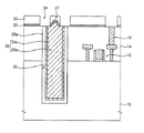
図13を参照すると、積層型半導体素子は第1集積回路チップ150、第2集積回路チップ152、はんだ50、及びコンタクト構造物112を含む。前記第1集積回路チップ150に含まれる素子はメモリ素子またはロジック素子でありうる。他の例として、前記第1集積回路チップ150に含まれる素子はイメージ素子でもある。
Referring to FIG. 13, the stacked semiconductor device includes a first
TSV構造物128aの底面及び絶縁膜パターン122bの底面が第1基板10aの底面の外へ露出していることを除いては、第1集積回路チップ150は、図1に示した半導体素子と同じ構成を有することができる。図13のTSV構造物128a及び絶縁膜パターン122bは、図1及び図2のTSV構造物28及び絶縁膜パターン22aと類似するように形成される。
The first
これに加えて、最上部の第2配線44及び第3金属間絶縁膜42上には第1保護膜46が備わることができる。前記第1保護膜46を貫通してはんだ50が形成されることができる。
In addition, a first
前記第1集積回路チップ150は第1基板10a、第1回路パターン12、下部配線16、第1層間絶縁膜14、及び絶縁膜パターン122bを含む。第1集積回路チップ150はTSV構造物128a及び導電性ライン36を含む。前記TSV構造物128aは第1層間絶縁膜14及び第1基板10aを貫通して形成される。図1及び図2のように、導電性ライン36がTSV構造物128aの上面の外郭平坦部上に形成され、前記上面の中心突出部上には形成されない。前記導電性ライン36は第1金属間絶縁膜32に取り囲まれる。
The first
第1上部配線40及び第2上部配線44、並びに第2金属間絶縁膜38及び第3金属間絶縁膜42が、第1集積回路チップ150内に含まれる。また、前記第2上部配線44を覆う第1保護膜46が備わり、はんだ50は第1保護膜46を貫通して第2上部配線44に接触する。
The first
前記第1基板10aは単結晶シリコン基板でありうる。前記第1基板10aは10〜100μmの厚さを有する。前記第1基板10aの底面がTSV構造物128aの底面と同じ平面に位置することができる。または、前記第1基板10a底面に比べて前記TSV構造物128aの底面が突出するように前記第1基板10aが位置することができる。
The
以下においては、前記第1基板10aを貫通するTSV構造物128aを説明する。
Hereinafter, the
前記第1基板10aを貫通するビアホール20が備わる。前記ビアホール20の側壁には円筒形状の絶縁膜パターン122bが備わる。前記絶縁膜パターン122b上にはバリア膜パターン124b及びシードパターン(図示せず)が備わる。前記シードパターン上に前記ビアホール20の残りを埋める導電パターン126aが備わる。
A via
前記導電パターン126aは低抵抗を有しながら第1基板10aをなす物質との熱膨張係数の2倍以上の熱膨張係数を有する金属物質を含む。一例として、前記導電パターン126aは銅、アルミニウム、金、インジウム、ニッケルなどを含むことができる。本実施形態においては半導体工程に適合した銅を含む。
The
前記TSV構造物128aは、半導体チップでアドレスまたはチップイネーブルなどのような電気信号パッド、ピンパワーシグナルパッド、パワーアンプモジュールなどと連結して、第1集積回路150と第2集積回路チップ152との間の電気的信号を伝達することができる。第2金属間絶縁膜38及び第3金属間絶縁膜42が、第1金属間絶縁膜32上に次々と形成される。導電性ライン36並びに第1上部配線40及び第2上部配線44が絶縁膜38、42を貫通して形成される。
The
前記第2上部配線44はパッド電極として使われることができ、これからは第1パッド電極44と言う。第2上部配線44をカバーする第1保護膜46が第3金属間絶縁膜42上に形成される。前記第1保護膜46は絶縁物質からなり、一例として、ポリイミド物質を含むことができる。
The second
前記第1パッド電極44と接触するはんだ50が備わることができる。図示はしていないが、前記はんだ50は印刷回路基板と接触することができる。これとは異なり、ワイヤーボンディングによって前記第1パッド電極44とリードフレームが電気的に連結されることができる。
一方、第2集積回路チップ152は第2基板100、前記第2基板100上に備わる第2回路パターン102、配線104、第2層間絶縁膜106、第2パッド電極108を含む。
Meanwhile, the second
前記第2集積回路チップ152に含まれた半導体素子は前記第1集積回路チップ150に含まれたものと同一の半導体素子であることもあり、互いに異なる半導体素子でもある。
The semiconductor elements included in the second
第2層間絶縁膜106上には配線104と接続される第2パッド電極108が備わる。前記第2パッド電極108は前記第1基板10aのTSV構造物128aに電気的に接続されている。第2層間絶縁膜106及び第2パッド電極108上には第2保護膜110が備わる。前記第2保護膜110はポリイミド物質からなることができる。
A
前記第1集積回路チップ150に含まれたTSV構造物128aと前記第2集積回路チップ152に含まれた第2パッド電極108との間には第2保護膜110を貫通して導電性を有するコンタクト構造物112が介在される。前記コンタクト構造物112で使われることのできる物質の例としては銀(Ag)はんだペーストを挙げることができる。
Between the
即ち、本実施形態に係る半導体素子は第1集積回路チップ150及び第2集積回路チップ152が積層された構造を有し、TSV構造物128aを通じて前記第1集積回路チップ150及び第2集積回路チップ152が電気的に接続される。また、本実施形態に係る積層型素子はTSV構造物128aと上部の導電性ライン36との間の接着特性が優れているため、信号伝達速度が速い。従って、半導体素子の電気的特性が良好、且つ高い信頼性を有する。
That is, the semiconductor device according to the present embodiment has a structure in which the first
図示はしていないが、第1集積回路チップと同一構造のTSV構造物を含む3つ以上の集積回路チップが垂直に積層されることができる。 Although not shown, three or more integrated circuit chips including a TSV structure having the same structure as the first integrated circuit chip may be stacked vertically.
図14〜図18は、図13に示した積層型半導体素子の製造方法を示す断面図である。 14 to 18 are cross-sectional views showing a method of manufacturing the stacked semiconductor element shown in FIG.
図14を参照すると、第1基板10上に第1回路パターン12を形成し、第1回路パターン12をカバーする第1層間絶縁膜14を第1基板10上に形成する。下部配線16が第1層間絶縁膜14を貫通して形成される。
Referring to FIG. 14, a
第1層間絶縁膜14及び第1基板10がパターニングされて内部にビアホール20を形成する。絶縁膜パターン122aと、バリア膜パターン124a及び導電パターン126aを含むTSV構造物128が図6と類似するようにビアホール20内に形成される。導電パターン126aは図10と類似するように中心突出部27を有する。
The first
図15を参照すると、前記TSV構造物128及び第1層間絶縁膜14上にバッファ膜30を形成する。前記バッファ膜30上に第1金属間絶縁膜32を形成する。前記第1金属間絶縁膜32及びバッファ膜30を貫通して導電性ライン36を形成し、TSV構造物128の外郭平坦部と電気的に接続され、下部配線16上に形成される。
Referring to FIG. 15, a
前記導電性ライン36は、図10と類似するように、TSV構造物128の突出部27とは接触しないように形成される。図7〜図10と類似するように、前記導電性ライン36及び第1金属間絶縁膜32上に第2金属間絶縁膜38及び第3金属間絶縁膜42、並びに第1上部配線40及び第2上部配線44を形成する。
The
図16を参照すると、第1保護膜46が第3金属間絶縁膜42上に形成されて第2上部配線44をカバーする。前記第1保護膜46はポリイミド物質を含むことができる。前記第1保護膜46の一部分を除去して第2上部配線44を露出させる第3開口48を形成する。
Referring to FIG. 16, the first
前記第1基板10、絶縁膜パターン122a、バリア膜パターン124a、及び導電パターン126aの底面をグラインディングを通じて除去して、前記導電パターン126aの底面を露出させる。前記工程を通して、第1基板10の厚さが減少する。残留する導電パターン126a及びバリア膜パターン124bはTSV構造物128aを定義する。絶縁膜パターン122bはビアホール内のTSV構造物128aを取り囲む。
The bottom surface of the
前記グラインディング工程を通して、導電パターン126aの底面が第1基板10aの底面と同一平面上に置かれることになる。しかし、本発明は導電パターン126aの底面が第1基板10aの底面から突出した実施形態にも適用される。
Through the grinding process, the bottom surface of the
絶縁膜パターン122bはビアホール20側壁上にシリンダ形状を有する。バリア膜パターン124bは絶縁膜パターン122bの側壁上にシリンダ形状を有する。バリア膜パターン124bは導電パターン126aを囲む。
The insulating
図17を参照すると、前記第1保護膜46に形成された第3開口48内にはんだ50を形成する。これで、TSV構造物128aを含む第1集積回路チップ150が完成される。
Referring to FIG. 17, the
図18を参照すると、第2基板100上に前記第1集積回路チップ150と接合するための第2集積回路チップ152を形成する。具体的に、前記第2基板100上に第2回路パターン102、配線104及び第2層間絶縁膜106を形成する。前記第2層間絶縁膜106上に前記配線104と電気的に接続する第2パッド電極108を形成する。前記第2パッド電極108は前記第1基板10aに形成されたTSV構造物128aと各々対向するように配置される。
Referring to FIG. 18, a second
前記第2パッド電極108をカバーする第2保護膜110が第2層間絶縁膜106上に形成される。次に、第2保護膜110をパターニングして、第2パッド電極108を露出させる第4開口(図示せず)を形成する。コンタクト構造物112が前記第4開口内に形成されて第2パッド電極108に電気的に接続する。
A
また、図13を参照すると、第1基板10aのTSV構造物128aの底面と第2基板100のコンタクト構造物112が互いに圧搾して第1集積回路チップ150及び第2集積回路チップ152を含む積層型半導体素子が完成される。
Referring to FIG. 13, the bottom surface of the
図19及び図20は各々本発明の一実施形態に係るビア構造物上に形成された開口を有する導電構造物を説明するための平面図である。 19 and 20 are each a plan view for explaining a conductive structure having an opening formed on a via structure according to an embodiment of the present invention.
以下にて説明する半導体素子は導電性ライン構造物の形状を除いては図1及び図2に示した半導体素子と同一である。 The semiconductor element described below is the same as the semiconductor element shown in FIGS. 1 and 2 except for the shape of the conductive line structure.
図19及び図20を参照すると、第1導電性ライン60a及び第2導電性ライン60bは、TSV構造物28の中心突出部27を露出する第1開口62a及び第2開口62bを含む。
Referring to FIGS. 19 and 20, the first
開口62a、62bの大きさは突出部27の大きさに依存する。第1開口62aは突出部27の大きさより大きく、TSV構造物28の大きさより小さい。第2開口62bは突出部27の大きさより大きく、導電性ライン60b方向に沿って延伸する。第2開口62bもやはりバリア膜パターン24a、絶縁膜パターン22a、及び第1層間絶縁膜14の上面の部分を露出させる。
The sizes of the
いかなる場合でも、各導電性ライン60a、60bは、TSV構造物28上面の5〜80%で接触する。
In any case, each
図19及び図20に示した半導体素子は、図3〜図8を参照して説明したことと同じ工程を遂行して形成される。ただし、第1開口34が形成される位置が異なる。次に、前記図9及び図10を参照で説明したのと同じ工程を遂行する。これで、図19及び図20の半導体素子を製造する。
The semiconductor device shown in FIGS. 19 and 20 is formed by performing the same process as described with reference to FIGS. However, the position where the
図21及び図22は本発明の一実施形態に係る複合ビア構造物上に形成された複合導電構造物を説明するための平面図である。 21 and 22 are plan views for explaining the composite conductive structure formed on the composite via structure according to the embodiment of the present invention.
以下において説明する半導体素子はTSV構造物上に形成される導電性ラインの形状を除いては図1及び図2に示した半導体素子と同一である。 The semiconductor element described below is the same as the semiconductor element shown in FIGS. 1 and 2 except for the shape of the conductive line formed on the TSV structure.
図21を参照すると、複合TSV構造物28a、28b上に一方向に延伸する導電性ライン64は、前記方向に沿って二つに分離される。導電性ライン64の各部分はTSV構造物28a、28b中、少なくとも一つの上面のうち外郭平坦部に接触する。導電性ライン64の前記の部分はTSV構造物28a、28bによって電気的に接続される。
Referring to FIG. 21, the
例示的な実施形態によると、導電性ライン64は三部分に分離される。導電性ライン64の一部分は両TSV構造物28a、28bの上面の外郭平坦部に接触する。導電性ライン64の他の部分は第1TSV構造物28aの上面の外郭平坦部に接触し、導電性ライン64のまた他の部分は第2TSV構造物28bの上面の外郭平坦部に接触する。
According to an exemplary embodiment,
導電性ライン64の前記部分はTSV構造物28a、28bの全体上面の5〜80%で接触する。
The portion of the
図21に示した半導体素子は、図3〜図10を参照して説明したのと同一工程を通して形成することができる。ただし、第1開口34の位置と形状のみが異なる。
The semiconductor element shown in FIG. 21 can be formed through the same process as described with reference to FIGS. However, only the position and shape of the
図22は本発明の一実施形態に係る半導体素子の平面図である。 FIG. 22 is a plan view of a semiconductor device according to an embodiment of the present invention.
図22に示した半導体素子は導電性ラインが追加的にさらに備わることを除いては、図1及び図2の半導体素子と同一構造を有する。 The semiconductor device shown in FIG. 22 has the same structure as the semiconductor device of FIGS. 1 and 2 except that a conductive line is additionally provided.
図22を参照すると、二つの導電性ライン36がTSV構造物28の上面の外郭平坦部の第1部分に接触する。第2導電性ライン37はTSV構造物28の中心部上で第1導電性ライン36間に平行するように延伸する二部分を含む。第2導電性ライン37の前記部分は第1導電性ライン36間にTSV構造物28の上面の外郭平坦部の部分に接触する。
Referring to FIG. 22, two
図22に示した半導体素子は、図3〜図10を参照して説明したのと同一工程を通して形成されることができる。ただし、第1開口34が形成される位置と形状が異なる。
The semiconductor device shown in FIG. 22 can be formed through the same process as described with reference to FIGS. However, the position and shape of the
図23は本発明の一実施形態に係る半導体素子内のビア構造物上に形成された追加導電構造物を含む断面図である。 FIG. 23 is a cross-sectional view including an additional conductive structure formed on a via structure in a semiconductor device according to an embodiment of the present invention.
以下において説明する半導体素子は、図1、図19、図20、図21、及び図22のように、導電性ライン36がTSV構造物28の外郭平坦部上で形成される。
In the semiconductor device described below, the
図23を参照すると、第1金属間絶縁膜32が導電性ライン構造物36を囲む。第2金属間絶縁膜38が第1金属間絶縁膜32及び導電性ライン構造物36上に形成される。上部配線40が第2金属間絶縁膜38を貫通して形成され、各々は上部導電性ライン40a及び上部コンタクト40bを含む。上部配線40は、図23のTSV構造物28の突出部27をオーバーラップしないように形成する。
Referring to FIG. 23, the first
TSV構造物28の突出部27上に形成された第2金属間絶縁膜38部分は平坦でないこともある。従って、上部配線40は突出部27にオーバーラップされないように形成して平坦に形成することができる。
The portion of the second
図23に示した半導体素子は図3〜図10を参照して説明したのと同一工程を通じて形成されることができる。ただし、上部配線40の位置のみが異なる。
The semiconductor device shown in FIG. 23 can be formed through the same process as described with reference to FIGS. However, only the position of the
図24及び図25は本発明の一実施形態に係る中心充填部を有するビア構造物を含む半導体素子の断面図である。 24 and 25 are cross-sectional views of a semiconductor device including a via structure having a center filling portion according to an embodiment of the present invention.
図24及び図25を参照すると、第1基板10上に第1回路パターン12が備わる。前記第1回路パターン12はトランジスタ、ダイオードなどを含むことができる。
Referring to FIGS. 24 and 25, the
前記第1基板10上には前記第1回路パターン12を覆う第1層間絶縁膜14が備わる。下部配線16が第1層間絶縁膜14を貫通して第1回路パターン12に接続される。ビアホール68が第1層間絶縁膜14及び第1基板10の少なくとも一部を貫通して形成される。前記ビアホール68は楕円形状を有することができる。
A first
前記ビアホール68の内壁上に絶縁膜パターン70aが備わる。前記絶縁膜パターン70a上にはバリア膜パターン72aが備わる。前記バリア膜パターン72aは、Ta、TaN、Ti、TiN、Ru、Co、Ni、NiB、WNなどの物質から形成することができる。これらは単独または2つ以上を積層して使うことができる。
An insulating
前記バリア膜パターン72a上には前記ビアホール68の残りを埋める導電パターン74aが備わる。導電パターン74aは中心充填部78aを取り囲むカップ形状を有する。前記導電パターン74aは低抵抗を有し、第1基板10をなすシリコンの熱膨張係数の2倍以上の熱膨張係数を有する金属からなることができる。前記導電パターン74aは銅(Cu)、アルミニウム、金、インジウム、ニッケルなどからなることができる。本実施形態では前記導電パターン74aは半導体製造工程に最も適合して低抵抗を有する銅を含むことができる。導電パターン74a及びバリア膜パターン72aはTSV構造物76を定義する。
A
中心充填部78aは前記ビアホール68の中心に形成される。前記中心充填部78aは絶縁物質または導電物質からなることができる。一例として、前記中心充填部78aはスピンオングラス(SOG)系列の酸化物、フロアブルシリコン(Flowable Si)、チタニウム、アルミニウム、多孔質物質(porous material)等を挙げることができる。
The
いかなる場合でも、中心充填部78aの物質は、導電パターン74a物質の熱膨張係数より3〜4倍低い熱膨張係数を有する。例えば、導電パターン74aは、17PPMの熱膨張係数を有する銅を含むことができる。この場合、中心充填部78aは、3〜4PPMの低い熱膨張係数を有する物質を含むことができる。
In any case, the material of the
導電パターン74aはカップ形状の導電パターン74aの上面中心部についてリング形状を有する突出部75を含む。中心充填部78a及び絶縁パターン70aに隣接するように配置される導電パターン74a上面の外郭部は第1層間絶縁膜14の上面と同一平面に位置することができる。
The
TSV構造物76及び第1層間絶縁膜14上部面を覆うバッファ膜30が備わる。複数の導電性ライン80aが形成されてTSV構造物76上面の外郭平坦部と接触し、または第1金属間絶縁膜32及びバッファ膜30を貫通して下部配線16と接触する。導電性ライン80aは突出部75上に形成されず、これと接触することもない。
A
二つの平行した導電性ライン80aがTSV構造物76の上面の外郭平坦部に接触する。これとは異なり、二個以上の導電性ライン80aがTSV構造物76の上面の平坦部に接触するように形成されることもできる。いかなる場合でも、導電性ライン80aは形成されてTSV構造物76の全体上面の5〜80%で接触する。
Two parallel
前記導電性ライン80aはバリア膜及び低抵抗を有する金属を含む導電膜を含む。前記金属は半導体製造工程に適合しながら低抵抗を有する銅を含むことができる。
The
前記第1金属間絶縁膜32上に第2金属間絶縁膜38が備わることができる。前記第2金属間絶縁膜38を貫通して前記導電性ライン80aと接続する上部配線40が備わることができる。これによって、上部配線40は導電性ライン80aに電気的に接続される接続構造物を形成することができる。図示はしていないが、前記第1上部配線40及び第2金属間絶縁膜38上に層間絶縁膜及び配線がさらに積層されることができる。
A second intermetallic insulating
図26及び図27は、図24及び図25に示した半導体素子を製造する方法を示す断面図である。 26 and 27 are cross-sectional views showing a method for manufacturing the semiconductor device shown in FIGS.
先に、図3及び図4を参照して説明したのと同一工程を遂行して、第1層間絶縁膜14にビアホール68及び絶縁膜70を形成する。この時、前記ビアホール68の上部面は円または楕円形状を有することができる。絶縁膜70はビアホール68の内壁上に形成され、また、第1層間絶縁膜14及び下部配線16上に形成されたエッチング阻止膜18上にも形成される。
The via
図26を参照すると、前記絶縁膜70上にバリア膜72を形成する。前記バリア膜72上に導電膜74を形成する。前記導電膜74は低抵抗を有し、第1基板10をなすシリコンの熱膨張係数の2倍以上の熱膨張係数を有する金属からなることができる。前記導電膜74は銅(Cu)、アルミニウム、金、インジウム、ニッケルなどからなることができる。本実施形態においては前記導電膜74は半導体製造工程に最も適合し、且つ低抵抗を有する銅を含むことができる。
Referring to FIG. 26, a
前記導電膜74上に前記ビアホール68の残りを埋める中心充填膜78を形成する。前記中心充填膜78はスピンオングラス(SOG)系列の酸化物、フロアブルシリコン(Flowable Si)、チタニウム、アルミニウム、多孔質物質(porous material)等を挙げることができる。一実施形態によると、導電膜74は17PPMの熱膨張係数を有する銅を含む。この場合、中心充填膜78は、3〜4PPMの低い熱膨張係数を有する物質を含むことができる。従って、中心充填膜78は導電膜74の熱膨張を緩衝して、リング形状の突出部75の高さを最小化する。
A
図27を参照すると、前記第1層間絶縁膜14の上部面が露出されるように前記中心充填膜78、導電膜74、バリア膜72、絶縁膜70及びエッチング阻止膜18を研磨する。これによって、TSV構造物76がビアホール68内に形成される。続いて、図7〜図10を参照して説明した工程を遂行する。それによって、図24に示した半導体素子を製造することができる。
Referring to FIG. 27, the
図28〜図30は本発明の一実施形態に係る複合ビア構造物上に形成された複合導電構造物を有する半導体素子の平面図である。 28 to 30 are plan views of a semiconductor device having a composite conductive structure formed on a composite via structure according to an embodiment of the present invention.
以下にて説明する半導体素子は、カップ形状で形成されたTSV構造物76a、76bが中心充填膜78a、78bを各々取り囲むことを除けば、図21に示した半導体素子と同一である。
The semiconductor element described below is the same as the semiconductor element shown in FIG. 21 except that the
図28を参照すると、導電性ライン81は複数個に分離し、複数個のTSV構造物76a、76bに沿って延伸する。各TSV構造物76a、76bは図27と類似するように形成する。導電性ライン81の各部分はTSV構造物76a、76bのうち、少なくとも一つの外郭平坦部に接触する。前記導電性ライン81の部分はTSV構造物76a、76bにより電気的に接続される。
Referring to FIG. 28, the
図28に示した実施形態において、導電性ライン81は三部分に分けられる。導電性ライン81の一部分は、TSV構造物76a、76bの上面の外郭平坦面部分に接触する。導電性ライン81の他の部分は、第1TSV構造物76aの上面の外郭平坦面の一部に接触し、導電性ライン81のまた他の部分は、第2TSV構造物76bの上面の外郭平坦面の一部に接触する。
In the embodiment shown in FIG. 28, the
第1TSV構造物76aは、第1導電パターン74a及び第1バリア膜パターン72aを含む。第2TSV構造物76bは、第2導電パターン74b及び第2バリア膜パターン72bを含む。各第1導電パターン74a及び第2導電パターン74bは、リング形状の中心突出部75を有する。
The
第1中心充填部78aは、第1導電パターン74aによって取り囲まれて、第2中心充填部78bは第2導電パターン74bによって取り囲まれる。
The first
図28に示した半導体素子は図26及び図27を参照して説明したのと同一工程を通じて形成することができる。ただし、導電性ライン構造物81の位置と形状のみが異なる。
The semiconductor element shown in FIG. 28 can be formed through the same process as described with reference to FIGS. However, only the position and shape of the
図29は本発明の一実施形態に係る半導体素子の平面図である。図29においては説明の便宜のために、TSV構造物及び導電性ラインのみを図示し、残りの部材は図24に示したものと類似している。 FIG. 29 is a plan view of a semiconductor device according to an embodiment of the present invention. In FIG. 29, only the TSV structure and the conductive line are shown for convenience of explanation, and the remaining members are similar to those shown in FIG.
図29を参照すると、輪状の導電パターンを含むTSV構造物90a、90b、90cが備わる。前記TSV構造物90a、90b、90cは図24に示したTSV構造物76と同一形状を有する。
Referring to FIG. 29,
本実施形態において、三つのTSV構造物90a、90b、90cはより大きい一つのTSV構造物92を形成することができる。即ち、直径が非常に広い一つのTSV構造物が要求される素子の場合、直径が非常に広い一つのTSV構造物を形成することが容易ではない。従って、狭い直径を有する複数のTSV構造物90a、90b、90cが実質的には一つのTSV構造物92の機能をするように提供する。相対的に小さい直径を有する各TSV構造物90a、90b、90cは最小化した突出部の高さを有する。
In the present embodiment, the three
前記各TSV構造物90a、90b、90cは、各中心充填部94を取り囲んで、輪(annular)状の突出部95を有する。各導電性ライン構造物96は、TSV構造物90a、90b、90cのうち、少なくとも二つを含む各セットの上面の外郭平坦部に接触する。各導電性ライン構造物96は、TSV構造物90a、90b、90cの突出部95には接触しない。
Each of the
前記導電性ライン96は図29に示したように、互いに平行するように延長し、複数個の部分に分離する。導電性ライン96の前記の部分はTSV構造物92によって電気的に接続する。導電性ライン92はTSV構造物90a、90b、90cの全体上面の5〜80%で接触する。
As shown in FIG. 29, the
図30は本発明の一実施形態に係る半導体素子の平面図である。説明の便宜のために図30にはTSV構造物及び導電性ラインだけが図示されている。しかし、図24と類似する追加構造物が図30の半導体素子のためにさらに形成されることもできる。一方、以下にて説明する半導体素子はTSV構造物93の形状を除いては図29に示した半導体素子と同一である。 FIG. 30 is a plan view of a semiconductor device according to an embodiment of the present invention. For convenience of explanation, only the TSV structure and the conductive lines are shown in FIG. However, additional structures similar to FIG. 24 may be further formed for the semiconductor device of FIG. On the other hand, the semiconductor element described below is the same as the semiconductor element shown in FIG. 29 except for the shape of the TSV structure 93.
図30を参照すると、各TSV構造物91a、91b、91cは、図1に示したTSV構造物28と同じ形状を有する。本実施形態において、互いに隣接する複数のTSV構造物91a、91b、91cは、より大きい一つであるTSV構造物93を定義する。各TSV構造物91a、91b、91cは中心突出部97を含む。
Referring to FIG. 30, each TSV structure 91a, 91b, 91c has the same shape as the
複数の導電性ライン構造物96がTSV構造物91a、91b、91cのうち、少なくとも二つを含むセットの外郭平坦部の部分上に形成されて接触する。導電性ライン96はTSV構造物91a、91b、91cの突出部97に接触しない。導電性ライン96は形成されてTSV構造物91a、91b、91cの間のラインに沿って延伸して互いに平行する。
A plurality of
導電性ライン96は複数個の部分に分離され、各部分はTSV構造物91a、91b、91cのうち、少なくとも二つを含むセットの外郭平坦部の部分上に形成して接触する。導電性ライン96の前記の部分はTSV構造物93によって電気的に接続される。導電性ライン96はTSV構造物91a、91b、91cの全体上面の5〜80%で接触する。図28〜図30の半導体素子において、上部配線(図示せず)もやはり導電性ラインの部分(81或いは96)を互いに接続する接続構造物として形成することが可能である。
The
図31〜図33は本発明の一実施形態に係る各積層半導体素子を有するシステムのブロックダイアグラムである。 31 to 33 are block diagrams of a system having each stacked semiconductor device according to an embodiment of the present invention.
図31は例えば、図13に示した積層型半導体素子を有するシステムのブロックダイアグラムである。 FIG. 31 is a block diagram of a system having the stacked semiconductor element shown in FIG. 13, for example.
図31を参照すると、システムはコントローラ520及びメモリ510を含む。メモリ510は例えば、図13に示した積層型メモリ素子を含む。前記メモリコントローラ520は、前記メモリの動作をコントロールするための入力信号を提供する。
Referring to FIG. 31, the system includes a
図32は例えば、図13に示した積層型半導体素子を有するシステムのブロックダイアグラムである。 FIG. 32 is a block diagram of a system having the stacked semiconductor element shown in FIG. 13, for example.
図32を参照すると、システムはホスト700及びメモリ510を含む。前記メモリ510は例えば、図13に示した積層型メモリ素子を含む。
Referring to FIG. 32, the system includes a
前記ホスト700はパーソナルコンピュータ、カメラ、モバイル機器、ゲーム機、通信機器などのような電子製品を含む。前記ホスト700はメモリ510を調節して作動させるための入力信号を印加し、前記メモリ510はデータ保存媒体として使われる。
The
図33は例えば、図13に示した積層型半導体素子を有するシステム600のブロックダイアグラムである。
FIG. 33 is a block diagram of a
図33を参照すると、前記システムは携帯用装置600であることができる。携帯用装置600はMP3プレーヤ、ビデオプレーヤ、ビデオとオーディオプレーヤの複合器などであることができる。携帯用装置600は例えば、図13に示した積層型メモリ素子のようなメモリ510を含む。
Referring to FIG. 33, the system can be a
図示したように、携帯用装置600はメモリ510、メモリコントローラ520、エンコーダ/デコーダ(EDC)610、表示部材620、及びインターフェース670を含むことができる。データ(オーディオ、ビデオなど)はエンコーダ/デコーダ(EDC)610によって前記メモリコントローラ520を経由して前記メモリ510から入/出力される。
As shown, the
エンコーダ/デコーダ(EDC)610はMP3プレーヤ或いはPMPプレーヤのようなメモリ510に保存されるオーディオ及び/または、ビデオデータをエンデコーディングする方法等を通じてメモリ510に保存されるデータをエンコーディングする。さらに、エンコーダ/デコーダ(EDC)610は、メモリ510内にビデオデータを保存するためのMPEGエンコーディングを行う。さらに、エンコーダ/デコーダ(EDC)610は複合エンコーダを含んでフォーマットにより互いに異なる類型のデータをエンコーディングする。例えば、エンコーダ/デコーダ(EDC)610はオーディオデータをエンコーディングするためのMP3エンコーダ或いはビデオデータをエンコーディングするためのMPEGエンコーダを含む。
An encoder / decoder (EDC) 610 encodes data stored in the
エンコーダ/デコーダ(EDC)610は、MP3プレーヤ或いはPMPプレーヤのようなメモリ510からMP3デコーディング或いはMPEGデコーディングする方法等を通じてメモリ510から出力されたデータをデコーディングする。さらに、エンコーダ/デコーダ(EDC)610は複合デコーダを含んで、フォーマットにより互いに異なる類型のデータをデコーディングする。例えば、エンコーダ/デコーダ(EDC)610はオーディオデータをデコーディングするためのMP3デコーダ或いはビデオデータをデコーディングするためのMPEGデコーダを含む。
The encoder / decoder (EDC) 610 decodes data output from the
他の実施形態によると、エンコーダ/デコーダ(EDC)610はデコーダのみを含む。例えば、エンコーディングしたデータはエンコーダ/デコーダ(EDC)610で入力され、以後、エンコーダ/デコーダ(EDC)610はメモリコントローラ520或いはメモリ510に伝送するために前記入力データをデコーディングすることができる。
According to another embodiment, encoder / decoder (EDC) 610 includes only a decoder. For example, encoded data is input by an encoder / decoder (EDC) 610, and the encoder / decoder (EDC) 610 can subsequently decode the input data for transmission to the
エンコーダ/デコーダ(EDC)610は、エンコーディングされるデータ或いはインターフェース670を通じてエンコーディングされるデータを受信することができる。インターフェース670は、確立されたインターフェース標準(例えば、FireWire、USBなど)にコンパイルしてFireWireインターフェース、USBインターフェースなどを含む。従って、データはインターフェース670を通じてメモリ510から出力されることができる。
An encoder / decoder (EDC) 610 can receive the encoded data or the encoded data through the
表示部材620はメモリ510から出力されてエンコーダ/デコーダ(EDC)610によりデコーディングされた使用者データを表示する。表示部材620の例として、オーディオデータを出力するスピーカー、ビデオデータを出力するディスプレースクリーンなどを挙げることができる。
The
以上、添付図面を参照しながら本発明の好適な実施形態について詳細に説明したが、本発明はかかる例に限定されない。本発明の属する技術の分野における通常の知識を有する者であれば、特徴請求の範囲に記載された技術的思想の範疇内において、各種の変更例または修正例に想到し得ることは明らかであり、これらについても、当然に本発明の技術的範囲に属するものと了解される。 The preferred embodiments of the present invention have been described in detail above with reference to the accompanying drawings, but the present invention is not limited to such examples. It is obvious that a person having ordinary knowledge in the technical field to which the present invention pertains can make various changes or modifications within the scope of the technical idea described in the claims. Of course, it is understood that these also belong to the technical scope of the present invention.
10 第1基板
12 第1回路パターン
14 第1層間絶縁膜
16 下部配線
18 エッチング阻止膜
20 ビアホール
22 絶縁膜
22a 絶縁膜パターン
24 バリア膜
24a バリア膜パターン
26 導電膜
26a 導電パターン
27 突出部
28 TSV構造物
30 バッファ膜
32 第1金属間絶縁膜
36 導電性ライン
38 第2金属間絶縁膜
40 第1上部配線
150 第1集積回路チップ
152 第2集積回路チップ
112 コンタクト構造物
42 第3金属間絶縁膜
44 第2上部配線
46 第1保護膜
50 はんだ
100 第2基板
102 第2回路パターン
104 配線
106 第2層間絶縁膜
108 第2パッド電極
110 第2保護膜
DESCRIPTION OF
Claims (24)
前記基板に埋め込まれ、平坦部及び前記平坦部に取り囲まれた突出部を含む表面を有し、前記基板よりも大きな熱膨張係数を有する材料からなるビア構造物と、
前記ビア構造物の前記平坦部のうち、少なくとも一部上に形成され、前記突出部のうち、少なくとも一部上には形成されない導電構造物と、を含む半導体素子。 A substrate,
A via structure made of a material embedded in the substrate and having a surface including a flat portion and a protruding portion surrounded by the flat portion, and having a larger thermal expansion coefficient than the substrate ;
And a conductive structure formed on at least a portion of the flat portion of the via structure and not formed on at least a portion of the protruding portion.
前記開口の内壁上に形成された絶縁膜と、
前記開口内の前記絶縁膜上に形成されたバリア膜と、
前記バリア膜が形成された前記開口内に形成されて前記バリア膜によって少なくとも一部が取り囲まれる導電パターンと、を含むことを特徴とする請求項6に記載の半導体素子。 The TSV is
An insulating film formed on the inner wall of the opening;
A barrier film formed on the insulating film in the opening;
The semiconductor element according to claim 6, further comprising: a conductive pattern formed in the opening in which the barrier film is formed and at least partially surrounded by the barrier film.
前記導電構造物及び前記他の導電構造物を結合する接続構造物と、をさらに含むことを特徴とする請求項1に記載の半導体素子。 Another conductive structure formed on at least a part of the flat portion of the via structure and not formed on the protrusion;
The semiconductor device according to claim 1, further comprising a connection structure that couples the conductive structure and the other conductive structure.
前記導電構造物は前記複合ビア構造物の平坦部上に形成され、前記突出部上には形成されないことを特徴とする請求項1に記載の半導体素子。 Further including other via structures having a surface including a flat portion and a protrusion,
The semiconductor device according to claim 1, wherein the conductive structure is formed on a flat portion of the composite via structure and is not formed on the protruding portion.
前記複数個のビア構造物のうち、少なくとも二つを含む各セットの平坦部上には形成され、突出部上には形成されない複数個の導電構造物をさらに含むことを特徴とする請求項1に記載の半導体素子。 A plurality of via structures each having a respective surface including a flat portion and a protrusion;
2. The conductive structure according to claim 1, further comprising a plurality of conductive structures formed on the flat portion of each set including at least two of the plurality of via structures, and not formed on the protrusions. The semiconductor element as described in.
前記第1集積回路チップの前記ビア構造物に結合されるコンタクト構造物を含む第2集積回路チップを具備する積層型半導体素子。 A via structure made of a material having a substrate and a surface including a flat portion and a protruding portion surrounded by the flat portion and having a larger thermal expansion coefficient than the substrate; and the via structure A first integrated circuit chip including a conductive structure formed on at least a portion of the flat portion and not formed on at least a portion of the protrusion;
A stacked semiconductor device comprising a second integrated circuit chip including a contact structure coupled to the via structure of the first integrated circuit chip.
前記ビア構造物の前記突出部上に形成され、及び前記導電構造物を取り囲む誘電膜と、をさらに含むことを特徴とする請求項17に記載の積層型半導体素子。 A buffer film formed on the protruding portion of the via structure;
The stacked semiconductor device of claim 17, further comprising a dielectric film formed on the projecting portion of the via structure and surrounding the conductive structure.
前記ビア構造物の前記外郭部のうち、少なくとも一部上に形成され、前記中心部上には形成されない導電構造物を含む半導体素子。 Center is a flat, outer portion is flat, and has a surface including a projecting portion disposed between said central portion and said outer portion, penetrating the semiconductor substrate, a large thermal expansion than the semiconductor substrate A via structure made of a material having a coefficient ;
A semiconductor device including a conductive structure formed on at least a part of the outer portion of the via structure and not formed on the central portion.
前記ビア構造物の前記外郭部のうち、少なくとも一部上に形成され、前記中心部上には形成されない導電構造物を含み、
前記ビア構造物の前記中心部は、前記外郭部から突出していることを特徴とする半導体素子。 A via structure made of a material having a thermal expansion coefficient larger than that of the semiconductor substrate, the surface including a central portion and a flat outer portion, and penetrating the semiconductor substrate;
A conductive structure formed on at least a part of the outer portion of the via structure and not formed on the center;
Wherein the central portion of the via structure, you characterized in that projecting from the outer portion semiconductors elements.
Applications Claiming Priority (4)
| Application Number | Priority Date | Filing Date | Title |
|---|---|---|---|
| KR1020100061080A KR101692434B1 (en) | 2010-06-28 | 2010-06-28 | Semiconductor device and method of manufacturing the same |
| KR10-2010-0061080 | 2010-06-28 | ||
| US12/913,748 | 2010-10-27 | ||
| US12/913,748 US8390120B2 (en) | 2010-06-28 | 2010-10-27 | Semiconductor device and method of fabricating the same |
Publications (3)
| Publication Number | Publication Date |
|---|---|
| JP2012009847A JP2012009847A (en) | 2012-01-12 |
| JP2012009847A5 JP2012009847A5 (en) | 2014-07-03 |
| JP5921822B2 true JP5921822B2 (en) | 2016-05-24 |
Family
ID=45351765
Family Applications (1)
| Application Number | Title | Priority Date | Filing Date |
|---|---|---|---|
| JP2011113410A Active JP5921822B2 (en) | 2010-06-28 | 2011-05-20 | Semiconductor device and manufacturing method thereof |
Country Status (4)
| Country | Link |
|---|---|
| US (1) | US8390120B2 (en) |
| JP (1) | JP5921822B2 (en) |
| KR (1) | KR101692434B1 (en) |
| CN (1) | CN102299136B (en) |
Families Citing this family (48)
| Publication number | Priority date | Publication date | Assignee | Title |
|---|---|---|---|---|
| US9831164B2 (en) * | 2010-06-28 | 2017-11-28 | Samsung Electronics Co., Ltd. | Semiconductor device and method of fabricating the same |
| US8659152B2 (en) * | 2010-09-15 | 2014-02-25 | Osamu Fujita | Semiconductor device |
| JP5733002B2 (en) * | 2011-04-28 | 2015-06-10 | 富士通セミコンダクター株式会社 | Manufacturing method of semiconductor device |
| US8541883B2 (en) * | 2011-11-29 | 2013-09-24 | Advanced Semiconductor Engineering, Inc. | Semiconductor device having shielded conductive vias |
| CN103187400B (en) * | 2011-12-31 | 2016-02-17 | 中芯国际集成电路制造(上海)有限公司 | Silicon through hole detection architecture and detection method |
| KR101918609B1 (en) * | 2012-01-11 | 2018-11-14 | 삼성전자 주식회사 | Integrated circuit device |
| US20150145144A1 (en) * | 2012-06-07 | 2015-05-28 | Rensselaer Polytechnic Institute | Use of a conformal coating elastic cushion to reduce through silicon vias (tsv) stress in 3-dimensional integration |
| US9275933B2 (en) * | 2012-06-19 | 2016-03-01 | United Microelectronics Corp. | Semiconductor device |
| US8956974B2 (en) * | 2012-06-29 | 2015-02-17 | Micron Technology, Inc. | Devices, systems, and methods related to planarizing semiconductor devices after forming openings |
| KR101965906B1 (en) * | 2012-07-12 | 2019-04-04 | 에스케이하이닉스 주식회사 | Semiconductor device |
| KR101960496B1 (en) * | 2012-08-29 | 2019-03-20 | 에스케이하이닉스 주식회사 | Semiconductor device |
| US9112007B2 (en) | 2012-09-14 | 2015-08-18 | Taiwan Semiconductor Manufacturing Company, Ltd. | Through via structure and method |
| KR101992352B1 (en) | 2012-09-25 | 2019-06-24 | 삼성전자주식회사 | Semicondctor devices |
| US8952542B2 (en) * | 2012-11-14 | 2015-02-10 | Advanced Semiconductor Engineering, Inc. | Method for dicing a semiconductor wafer having through silicon vias and resultant structures |
| KR20140073163A (en) | 2012-12-06 | 2014-06-16 | 삼성전자주식회사 | Semiconductor device and method of forming the same |
| US8921150B2 (en) * | 2012-12-06 | 2014-12-30 | Taiwan Semiconductor Manufacturing Co., Ltd. | Process to achieve contact protrusion for single damascene via |
| US9761481B2 (en) * | 2013-01-23 | 2017-09-12 | GlobalFoundries, Inc. | Integrated circuits and methods of forming the same with metal layer connection to through-semiconductor via |
| CN104051491B (en) * | 2013-03-15 | 2017-06-06 | 新加坡商格罗方德半导体私人有限公司 | Nonvolatile memory device with through-silicon intermediary/silicon guide hole application |
| US9059111B2 (en) * | 2013-04-11 | 2015-06-16 | International Business Machines Corporation | Reliable back-side-metal structure |
| US9287173B2 (en) * | 2013-05-23 | 2016-03-15 | United Microelectronics Corp. | Through silicon via and process thereof |
| CN103280427B (en) * | 2013-06-13 | 2016-08-10 | 华进半导体封装先导技术研发中心有限公司 | A kind of TSV front side end interconnection process |
| US9147642B2 (en) * | 2013-10-31 | 2015-09-29 | Nanya Technology Corporation | Integrated circuit device |
| US9476927B2 (en) | 2014-01-22 | 2016-10-25 | GlobalFoundries, Inc. | Structure and method to determine through silicon via build integrity |
| CN103794554A (en) * | 2014-02-27 | 2014-05-14 | 华进半导体封装先导技术研发中心有限公司 | Improved preparation method of through silicon via structure |
| CN103811416B (en) * | 2014-02-27 | 2017-01-04 | 华进半导体封装先导技术研发中心有限公司 | The flattening method of through-silicon via sidewall |
| KR102161263B1 (en) * | 2014-04-04 | 2020-10-05 | 삼성전자주식회사 | Semicoductor device having through eleectrode capped by self-aligned protective layer |
| CN105336569B (en) * | 2014-07-10 | 2019-01-18 | 中国科学院微电子研究所 | Semiconductor device manufacturing method |
| KR102303983B1 (en) | 2014-09-22 | 2021-09-23 | 삼성전자주식회사 | Semiconductor devices and methods of manufacturing the same, and semiconductor packages including the semiconductor devices |
| KR102400185B1 (en) | 2014-11-12 | 2022-05-20 | 삼성전자주식회사 | Semiconductor dervices having through electrodes |
| CN104600027B (en) * | 2015-01-30 | 2017-10-27 | 华进半导体封装先导技术研发中心有限公司 | A kind of preparation technology of TSV through hole |
| CN104749846B (en) | 2015-04-17 | 2017-06-30 | 京东方科技集团股份有限公司 | A kind of array base palte and preparation method thereof, display panel |
| KR102444823B1 (en) | 2015-08-13 | 2022-09-20 | 삼성전자주식회사 | Semiconductor devices having through electrodes and methods for fabricating the same |
| KR102497205B1 (en) | 2016-03-03 | 2023-02-09 | 삼성전자주식회사 | Semiconductor devices having through electrodes and methods for fabricating the same |
| US9812414B1 (en) * | 2016-06-17 | 2017-11-07 | Nanya Technology Corporation | Chip package and a manufacturing method thereof |
| US9917009B2 (en) * | 2016-08-04 | 2018-03-13 | Globalfoundries Inc. | Methods of forming a through-substrate-via (TSV) and a metallization layer after formation of a semiconductor device |
| KR102542614B1 (en) | 2017-10-30 | 2023-06-15 | 삼성전자주식회사 | Image sensor |
| US11843020B2 (en) | 2017-10-30 | 2023-12-12 | Samsung Electronics Co., Ltd. | Image sensor |
| KR102652452B1 (en) * | 2018-06-29 | 2024-03-29 | 삼성디스플레이 주식회사 | Display device and method for manufacturing thereof |
| JP2020038900A (en) * | 2018-09-04 | 2020-03-12 | キオクシア株式会社 | Semiconductor device |
| KR102652444B1 (en) * | 2019-01-11 | 2024-03-28 | 삼성전자주식회사 | Image sensor |
| US10867855B2 (en) * | 2019-05-13 | 2020-12-15 | Honeywell International Inc. | Through silicon via fabrication |
| TWI778594B (en) * | 2020-05-26 | 2022-09-21 | 台灣積體電路製造股份有限公司 | Integrated circuit and method for manufacturing the same |
| CN114512469A (en) * | 2020-11-16 | 2022-05-17 | 长鑫存储技术有限公司 | Semiconductor structure and manufacturing method thereof |
| CN115376993A (en) * | 2021-05-19 | 2022-11-22 | 长鑫存储技术有限公司 | Chip, memory and preparation method of chip |
| US20220375824A1 (en) * | 2021-05-19 | 2022-11-24 | Changxin Memory Technologies, Inc. | Die, memory and method of manufacturing die |
| KR20230009205A (en) | 2021-07-08 | 2023-01-17 | 삼성전자주식회사 | Semiconductor chip and semiconductor package including the same |
| CN116264184A (en) * | 2021-12-15 | 2023-06-16 | 长鑫存储技术有限公司 | Semiconductor structure and manufacturing method thereof |
| CN116646321A (en) * | 2023-06-08 | 2023-08-25 | 武汉新芯集成电路制造有限公司 | Semiconductor structure and forming method thereof |
Family Cites Families (19)
| Publication number | Priority date | Publication date | Assignee | Title |
|---|---|---|---|---|
| DK0613610T3 (en) * | 1992-09-24 | 1997-08-25 | Hughes Aircraft Co | Penetrations with magnetizable material in a multilayer circuit structure |
| US5378927A (en) * | 1993-05-24 | 1995-01-03 | International Business Machines Corporation | Thin-film wiring layout for a non-planar thin-film structure |
| JP4011695B2 (en) * | 1996-12-02 | 2007-11-21 | 株式会社東芝 | Chip for multi-chip semiconductor device and method for forming the same |
| US6809421B1 (en) * | 1996-12-02 | 2004-10-26 | Kabushiki Kaisha Toshiba | Multichip semiconductor device, chip therefor and method of formation thereof |
| JP3687435B2 (en) * | 1999-08-27 | 2005-08-24 | セイコーエプソン株式会社 | Semiconductor chip and manufacturing method thereof, semiconductor device, computer, circuit board, and electronic device |
| KR100363702B1 (en) * | 2000-12-29 | 2002-12-05 | 주식회사 하이닉스반도체 | Storage node contact plug of semiconductor device and method for forming thereof |
| JP3891299B2 (en) * | 2003-05-06 | 2007-03-14 | セイコーエプソン株式会社 | Semiconductor device manufacturing method, semiconductor device, semiconductor device, electronic device |
| JP2005150299A (en) * | 2003-11-13 | 2005-06-09 | Seiko Epson Corp | Semiconductor chip, semiconductor device, method of manufacturing the same, circuit board, and electronic equipment |
| US7485968B2 (en) * | 2005-08-11 | 2009-02-03 | Ziptronix, Inc. | 3D IC method and device |
| TWI416663B (en) * | 2005-08-26 | 2013-11-21 | Hitachi Ltd | Semiconductor device manufacturing method and semiconductor device |
| US7633167B2 (en) * | 2005-09-29 | 2009-12-15 | Nec Electronics Corporation | Semiconductor device and method for manufacturing same |
| JP5021992B2 (en) * | 2005-09-29 | 2012-09-12 | ルネサスエレクトロニクス株式会社 | Semiconductor device and manufacturing method thereof |
| JP2008305938A (en) | 2007-06-07 | 2008-12-18 | Toshiba Corp | Semiconductor device, and manufacturing method thereof |
| JP5089336B2 (en) | 2007-10-29 | 2012-12-05 | 新光電気工業株式会社 | Silicon substrate for package |
| JP2009252924A (en) * | 2008-04-04 | 2009-10-29 | Toshiba Corp | Semiconductor device and method of manufacturing the same |
| JP5343245B2 (en) | 2008-05-15 | 2013-11-13 | 新光電気工業株式会社 | Manufacturing method of silicon interposer |
| US8183673B2 (en) * | 2008-10-21 | 2012-05-22 | Samsung Electronics Co., Ltd. | Through-silicon via structures providing reduced solder spreading and methods of fabricating the same |
| US7687311B1 (en) * | 2008-11-13 | 2010-03-30 | Taiwan Semiconductor Manufacturing Company, Ltd. | Method for producing stackable dies |
| JP2011228419A (en) * | 2010-04-19 | 2011-11-10 | Renesas Electronics Corp | Semiconductor integrated circuit device and method for manufacturing the same |
-
2010
- 2010-06-28 KR KR1020100061080A patent/KR101692434B1/en active IP Right Grant
- 2010-10-27 US US12/913,748 patent/US8390120B2/en active Active
-
2011
- 2011-05-20 JP JP2011113410A patent/JP5921822B2/en active Active
- 2011-06-10 CN CN201110154632.XA patent/CN102299136B/en active Active
Also Published As
| Publication number | Publication date |
|---|---|
| KR101692434B1 (en) | 2017-01-18 |
| CN102299136B (en) | 2016-03-02 |
| US8390120B2 (en) | 2013-03-05 |
| KR20120000690A (en) | 2012-01-04 |
| JP2012009847A (en) | 2012-01-12 |
| US20110316168A1 (en) | 2011-12-29 |
| CN102299136A (en) | 2011-12-28 |
Similar Documents
| Publication | Publication Date | Title |
|---|---|---|
| JP5921822B2 (en) | Semiconductor device and manufacturing method thereof | |
| JP5916077B2 (en) | Manufacturing method of semiconductor device | |
| JP6548377B2 (en) | Integrated circuit device and method of manufacturing the same | |
| US9214411B2 (en) | Integrated circuit devices including a through-silicon via structure and methods of fabricating the same | |
| KR101677507B1 (en) | Method of manufacturing semiconductor devices | |
| KR102064863B1 (en) | Method of fabricating Semiconductor Devices Having TSV | |
| US8076234B1 (en) | Semiconductor device and method of fabricating the same including a conductive structure is formed through at least one dielectric layer after forming a via structure | |
| KR101992352B1 (en) | Semicondctor devices | |
| US8987869B2 (en) | Integrated circuit devices including through-silicon-vias having integral contact pads | |
| JP3891299B2 (en) | Semiconductor device manufacturing method, semiconductor device, semiconductor device, electronic device | |
| US9018768B2 (en) | Integrated circuit having through silicon via structure with minimized deterioration | |
| US9530726B2 (en) | Semiconductor device and method of fabricating the same | |
| TWI546872B (en) | Electronic device and semiconductor device | |
| KR20120090417A (en) | Semiconductor device and method of manufacturing a semiconductor device | |
| US9831164B2 (en) | Semiconductor device and method of fabricating the same | |
| US10763163B2 (en) | Integrated circuit device and method of manufacturing the same | |
| JP2008288595A (en) | Semiconductor package, manufacturing method thereof, package module using semiconductor package, and electronic product | |
| JP2010045371A (en) | Through-silicon-via structure including conductive protective film, and method of forming the same | |
| KR20140073163A (en) | Semiconductor device and method of forming the same | |
| CN110875271A (en) | Semiconductor chip and method for manufacturing the same | |
| JP2011003645A (en) | Semiconductor device, and method of manufacturing the same | |
| JP2013070057A (en) | Semiconductor chip, semiconductor package including semiconductor chip, and manufacturing methods of semiconductor chip and semiconductor package | |
| KR101960686B1 (en) | Semiconductor device and method of forming the same | |
| US9059067B2 (en) | Semiconductor device with interposer and method manufacturing same | |
| KR20140063271A (en) | Semiconductor devices having through vias and methods of fabricating the same |
Legal Events
| Date | Code | Title | Description |
|---|---|---|---|
| A521 | Request for written amendment filed |
Free format text: JAPANESE INTERMEDIATE CODE: A523 Effective date: 20140516 |
|
| A621 | Written request for application examination |
Free format text: JAPANESE INTERMEDIATE CODE: A621 Effective date: 20140516 |
|
| RD04 | Notification of resignation of power of attorney |
Free format text: JAPANESE INTERMEDIATE CODE: A7424 Effective date: 20141226 |
|
| A977 | Report on retrieval |
Free format text: JAPANESE INTERMEDIATE CODE: A971007 Effective date: 20150422 |
|
| A131 | Notification of reasons for refusal |
Free format text: JAPANESE INTERMEDIATE CODE: A131 Effective date: 20150501 |
|
| A521 | Request for written amendment filed |
Free format text: JAPANESE INTERMEDIATE CODE: A523 Effective date: 20150710 |
|
| TRDD | Decision of grant or rejection written | ||
| A01 | Written decision to grant a patent or to grant a registration (utility model) |
Free format text: JAPANESE INTERMEDIATE CODE: A01 Effective date: 20160314 |
|
| A61 | First payment of annual fees (during grant procedure) |
Free format text: JAPANESE INTERMEDIATE CODE: A61 Effective date: 20160413 |
|
| R150 | Certificate of patent or registration of utility model |
Ref document number: 5921822 Country of ref document: JP Free format text: JAPANESE INTERMEDIATE CODE: R150 |
|
| R250 | Receipt of annual fees |
Free format text: JAPANESE INTERMEDIATE CODE: R250 |
|
| R250 | Receipt of annual fees |
Free format text: JAPANESE INTERMEDIATE CODE: R250 |
|
| R250 | Receipt of annual fees |
Free format text: JAPANESE INTERMEDIATE CODE: R250 |
|
| R250 | Receipt of annual fees |
Free format text: JAPANESE INTERMEDIATE CODE: R250 |
|
| R250 | Receipt of annual fees |
Free format text: JAPANESE INTERMEDIATE CODE: R250 |
|
| R250 | Receipt of annual fees |
Free format text: JAPANESE INTERMEDIATE CODE: R250 |