JP5847472B2 - Detection device and detection system - Google Patents
Detection device and detection system Download PDFInfo
- Publication number
- JP5847472B2 JP5847472B2 JP2011159011A JP2011159011A JP5847472B2 JP 5847472 B2 JP5847472 B2 JP 5847472B2 JP 2011159011 A JP2011159011 A JP 2011159011A JP 2011159011 A JP2011159011 A JP 2011159011A JP 5847472 B2 JP5847472 B2 JP 5847472B2
- Authority
- JP
- Japan
- Prior art keywords
- unit
- thin film
- film transistor
- circuit
- input
- Prior art date
- Legal status (The legal status is an assumption and is not a legal conclusion. Google has not performed a legal analysis and makes no representation as to the accuracy of the status listed.)
- Active
Links
- 238000001514 detection method Methods 0.000 title claims description 54
- 239000010409 thin film Substances 0.000 claims description 169
- 238000006243 chemical reaction Methods 0.000 claims description 27
- 239000003990 capacitor Substances 0.000 claims description 24
- 239000000758 substrate Substances 0.000 claims description 20
- 230000005855 radiation Effects 0.000 claims description 15
- 239000011159 matrix material Substances 0.000 claims description 3
- 230000005540 biological transmission Effects 0.000 claims description 2
- 239000004065 semiconductor Substances 0.000 description 22
- 239000012535 impurity Substances 0.000 description 9
- 229910021420 polycrystalline silicon Inorganic materials 0.000 description 7
- 239000000463 material Substances 0.000 description 6
- 230000007423 decrease Effects 0.000 description 5
- 238000000034 method Methods 0.000 description 5
- 229910021417 amorphous silicon Inorganic materials 0.000 description 4
- 238000010586 diagram Methods 0.000 description 4
- 230000003071 parasitic effect Effects 0.000 description 4
- 239000010408 film Substances 0.000 description 3
- 238000003384 imaging method Methods 0.000 description 2
- 229910021421 monocrystalline silicon Inorganic materials 0.000 description 2
- 239000002245 particle Substances 0.000 description 2
- 238000002161 passivation Methods 0.000 description 2
- 230000001960 triggered effect Effects 0.000 description 2
- XUIMIQQOPSSXEZ-UHFFFAOYSA-N Silicon Chemical compound [Si] XUIMIQQOPSSXEZ-UHFFFAOYSA-N 0.000 description 1
- 238000004458 analytical method Methods 0.000 description 1
- JJWKPURADFRFRB-UHFFFAOYSA-N carbonyl sulfide Chemical compound O=C=S JJWKPURADFRFRB-UHFFFAOYSA-N 0.000 description 1
- 238000003745 diagnosis Methods 0.000 description 1
- 238000005516 engineering process Methods 0.000 description 1
- 229910052732 germanium Inorganic materials 0.000 description 1
- GNPVGFCGXDBREM-UHFFFAOYSA-N germanium atom Chemical compound [Ge] GNPVGFCGXDBREM-UHFFFAOYSA-N 0.000 description 1
- 239000011521 glass Substances 0.000 description 1
- 238000007689 inspection Methods 0.000 description 1
- 239000011810 insulating material Substances 0.000 description 1
- CNQCVBJFEGMYDW-UHFFFAOYSA-N lawrencium atom Chemical compound [Lr] CNQCVBJFEGMYDW-UHFFFAOYSA-N 0.000 description 1
- 239000004973 liquid crystal related substance Substances 0.000 description 1
- 238000012423 maintenance Methods 0.000 description 1
- 238000004519 manufacturing process Methods 0.000 description 1
- 230000003287 optical effect Effects 0.000 description 1
- 229910052710 silicon Inorganic materials 0.000 description 1
- 239000010703 silicon Substances 0.000 description 1
Images


Classifications
-
- H—ELECTRICITY
- H04—ELECTRIC COMMUNICATION TECHNIQUE
- H04N—PICTORIAL COMMUNICATION, e.g. TELEVISION
- H04N5/00—Details of television systems
- H04N5/30—Transforming light or analogous information into electric information
- H04N5/32—Transforming X-rays
-
- H—ELECTRICITY
- H01—ELECTRIC ELEMENTS
- H01L—SEMICONDUCTOR DEVICES NOT COVERED BY CLASS H10
- H01L27/00—Devices consisting of a plurality of semiconductor or other solid-state components formed in or on a common substrate
- H01L27/14—Devices consisting of a plurality of semiconductor or other solid-state components formed in or on a common substrate including semiconductor components sensitive to infrared radiation, light, electromagnetic radiation of shorter wavelength or corpuscular radiation and specially adapted either for the conversion of the energy of such radiation into electrical energy or for the control of electrical energy by such radiation
- H01L27/144—Devices controlled by radiation
- H01L27/146—Imager structures
- H01L27/14601—Structural or functional details thereof
- H01L27/14609—Pixel-elements with integrated switching, control, storage or amplification elements
-
- H—ELECTRICITY
- H01—ELECTRIC ELEMENTS
- H01L—SEMICONDUCTOR DEVICES NOT COVERED BY CLASS H10
- H01L27/00—Devices consisting of a plurality of semiconductor or other solid-state components formed in or on a common substrate
- H01L27/14—Devices consisting of a plurality of semiconductor or other solid-state components formed in or on a common substrate including semiconductor components sensitive to infrared radiation, light, electromagnetic radiation of shorter wavelength or corpuscular radiation and specially adapted either for the conversion of the energy of such radiation into electrical energy or for the control of electrical energy by such radiation
- H01L27/144—Devices controlled by radiation
- H01L27/146—Imager structures
- H01L27/14643—Photodiode arrays; MOS imagers
- H01L27/14658—X-ray, gamma-ray or corpuscular radiation imagers
- H01L27/14663—Indirect radiation imagers, e.g. using luminescent members
-
- H—ELECTRICITY
- H01—ELECTRIC ELEMENTS
- H01L—SEMICONDUCTOR DEVICES NOT COVERED BY CLASS H10
- H01L27/00—Devices consisting of a plurality of semiconductor or other solid-state components formed in or on a common substrate
- H01L27/14—Devices consisting of a plurality of semiconductor or other solid-state components formed in or on a common substrate including semiconductor components sensitive to infrared radiation, light, electromagnetic radiation of shorter wavelength or corpuscular radiation and specially adapted either for the conversion of the energy of such radiation into electrical energy or for the control of electrical energy by such radiation
- H01L27/144—Devices controlled by radiation
- H01L27/146—Imager structures
- H01L27/14683—Processes or apparatus peculiar to the manufacture or treatment of these devices or parts thereof
- H01L27/14692—Thin film technologies, e.g. amorphous, poly, micro- or nanocrystalline silicon
-
- H—ELECTRICITY
- H04—ELECTRIC COMMUNICATION TECHNIQUE
- H04N—PICTORIAL COMMUNICATION, e.g. TELEVISION
- H04N25/00—Circuitry of solid-state image sensors [SSIS]; Control thereof
- H04N25/70—SSIS architectures; Circuits associated therewith
- H04N25/71—Charge-coupled device [CCD] sensors; Charge-transfer registers specially adapted for CCD sensors
- H04N25/745—Circuitry for generating timing or clock signals
Description
本発明は、医療用画像診断装置、非破壊検査装置、放射線を用いた分析装置などに応用される、検出装置および検出システムに関する。 The present invention relates to a detection apparatus and a detection system applied to a medical image diagnostic apparatus, a nondestructive inspection apparatus, an analysis apparatus using radiation, and the like.
薄膜半導体製造技術は、薄膜トランジスタ(TFT)等のスイッチ素子と光電変換素子等の変換素子とを組み合わせた画素のアレイ(画素アレイ)を有する検出装置に利用されている。従来の検出装置は、150〜200μmのピッチで画素がアレイ状に配列された、例えば43cm×43cmの基板が用いられてきた。そして、駆動配線を介して画素アレイを行単位で駆動するための駆動回路や、行単位で駆動された画素アレイから信号配線を介して並列に入力した信号を直列な信号として出力する読出回路が、単結晶シリコンの集積回路で準備される。そして駆動回路や読出回路が、その基板にチップオングラス実装されて、検出装置が構成されている。 The thin film semiconductor manufacturing technology is used for a detection device having an array of pixels (pixel array) in which a switching element such as a thin film transistor (TFT) and a conversion element such as a photoelectric conversion element are combined. Conventional detectors have used a substrate of 43 cm × 43 cm, for example, in which pixels are arranged in an array at a pitch of 150 to 200 μm. A driving circuit for driving the pixel array in units of rows through the driving wiring, and a readout circuit for outputting signals input in parallel through the signal wiring from the pixel array driven in units of rows as serial signals. Prepared with an integrated circuit of single crystal silicon. A driving circuit and a reading circuit are mounted on the substrate in a chip-on-glass manner to constitute a detection device.
このような検出装置では、近年、従来の基板のサイズを維持したまま、画素の小ピッチ化が求められており、50〜80μmのピッチの画素アレイが要求されている。そのため、単結晶シリコンの集積回路で準備された駆動回路を画素アレイが備えられた基板にチップオングラス実装することが困難となる。また、画素の小ピッチ化だけでなく、部品点数の削減や基板に対する画素アレイの専有面積増大化のため、駆動回路等をTFTプロセスで基板上に一体形成するシステムオンパネル化が求められている。 In such a detection apparatus, in recent years, it is required to reduce the pitch of pixels while maintaining the size of a conventional substrate, and a pixel array having a pitch of 50 to 80 μm is required. Therefore, it becomes difficult to mount a drive circuit prepared by an integrated circuit of single crystal silicon on a substrate provided with a pixel array. In addition to reducing the pitch of pixels, in order to reduce the number of components and increase the area occupied by the pixel array with respect to the substrate, there is a need for a system-on-panel configuration in which drive circuits and the like are integrally formed on the substrate by a TFT process. .
一方、TFTを用いた液晶表示装置では、駆動回路等をTFTプロセスで基板上に一体形成するシステムオンパネル化が進められている。非特許文献1には、TFTプロセスで基板上に一体形成され、画素の行単位で準備された単位回路が、駆動配線に対応して複数段設けられた駆動回路が開示されている。この単位回路は、出力部と、第1入力部と、第2入力部と、第3入力部と、第4入力部と、を含む。ここで、第1入力部は、スタート信号又は前段の単位回路の出力信号が入力される部分であり、出力部は、スイッチ素子の導通電圧と非導通電圧を含む出力信号を駆動配線に供給するために駆動配線に接続される部分である。また、第2入力部は、クロック信号が入力される部分であり、第3入力部は、スイッチ素子の非導通電圧が入力される部分であり、第4入力部は、リセット信号又は後段の単位回路の出力信号が入力される部分である。そして、単位回路は、出力部に一方の端子が接続された第1容量素子と、第1入力部と第1容量素子の他方の端子との間で第1容量素子に直列に接続された第1薄膜トランジスタと、第2入力部と出力部との間に設けられた第2薄膜トランジスタと、を含む。第1薄膜トランジスタは、そのソース及びドレインの一方とゲートが第1入力部に接続され、ソース及びドレインの他方が第1容量素子の他方の端子に第1節点Pで接続される。第2薄膜トランジスタは、そのゲートが第1節点Pと接続され、ソース及びドレインの一方が第2入力部と接続され、ソース及びドレインの他方が出力部と接続される。また、この単位回路は、第3入力部と第1容量素子の他方の端子との間で第1容量素子と直列に接続された第3薄膜トランジスタと、第3入力部と出力部との間に設けられた第4薄膜トランジスタと、を含む。第3薄膜トランジスタは、そのゲートが第2節点Qと接続され、ソース及びドレインの一方が第3入力部に接続され、ソース及びドレインの他方が第1容量素子の他方の端子に第1節点Pで接続される。第4薄膜トランジスタは、そのゲートが第2節点Qと接続され、ソース及びドレインの一方が第3入力部と接続され、ソース及びドレインの他方が出力部と接続される。また、この単位回路は、第3入力部と第4薄膜トランジスタのゲートとの間に設けられた第2容量素子を含む。
On the other hand, in a liquid crystal display device using a TFT, a system-on-panel structure in which a drive circuit and the like are integrally formed on a substrate by a TFT process is being advanced. Non-Patent
更に、この単位回路は、第4入力部と第2及び第4薄膜トランジスタのゲートとの間に設けられた第5薄膜トランジスタと、第2容量素子に並列に設けられた第6薄膜トランジスタと、を含む。第2容量素子は、その一方の端子が第3入力部に接続され、他方の端子が第4薄膜トランジスタのゲートに第2節点Qで接続される。第5薄膜トランジスタは、そのソース及びドレインの一方とゲートが第4入力部に接続され、ソース及びドレインの他方が第2節点Qと接続される。第6薄膜トランジスタは、そのゲートが第1入力部に接続され、ソース及びドレインの一方が第3入力部に接続され、ソース及びドレインの他方が第2節点Qと接続される。ここで、第1〜6の各薄膜トランジスタの閾値電圧をVthと、第3入力部以外の単位回路の各部に入力される信号の最大電圧値をVDDと、最小電圧値をVSSと、する。また、第2入力部に供給される非導通電圧もVssとする。この単位回路は、第1及び第2薄膜トランジスタと第1容量素子により、当該単位回路が選択された際には、第3入力部に入力されるクロック信号の最大電圧値であるVDDを出力する、所謂ブートストラップ動作を行うことができる。また、この単位回路は、第5及び第6薄膜トランジスタと第2容量素子により、当該単位回路が非選択の際には、非導通電圧を出力することができる。つまり、第1及び第2薄膜トランジスタと第1容量素子は、当該単位回路が選択された際に画素のスイッチ素子の導通電圧として第2入力部に入力されるクロック信号の最大値であるVDDを出力部に供給する回路として機能する。また、第3〜第6薄膜トランジスタと第2容量素子は、当該単位回路が非選択の際に非導通電圧VSSを出力部に供給する回路として機能する。 The unit circuit further includes a fifth thin film transistor provided between the fourth input portion and the gates of the second and fourth thin film transistors, and a sixth thin film transistor provided in parallel with the second capacitor element. One terminal of the second capacitive element is connected to the third input unit, and the other terminal is connected to the gate of the fourth thin film transistor at the second node Q. The fifth thin film transistor has one of a source and a drain and a gate connected to the fourth input unit, and the other of the source and the drain connected to the second node Q. The sixth thin film transistor has a gate connected to the first input unit, one of the source and the drain connected to the third input unit, and the other of the source and the drain connected to the second node Q. Here, the Vth of the first to sixth threshold voltage of each thin film transistor, and V DD the maximum voltage value of the signal inputted to each part of the unit circuit other than the third input section, and V SS a minimum voltage value, . The non-conduction voltage supplied to the second input unit is also Vss. The unit circuit outputs V DD that is the maximum voltage value of the clock signal input to the third input unit when the unit circuit is selected by the first and second thin film transistors and the first capacitor. A so-called bootstrap operation can be performed. Further, the unit circuit can output a non-conducting voltage when the unit circuit is not selected by the fifth and sixth thin film transistors and the second capacitor element. In other words, the first and second thin film transistors and the first capacitor element obtain V DD that is the maximum value of the clock signal input to the second input unit as the conduction voltage of the switch element of the pixel when the unit circuit is selected. It functions as a circuit that supplies the output unit. The third to sixth thin film transistors and the second capacitor element function as a circuit that supplies the non-conduction voltage VSS to the output unit when the unit circuit is not selected.
薄膜トランジスタにはリーク電流(チャネルリーク)が存在するため、上記単位回路において、特に非選択の際の非導通電圧の維持に課題がある。これは、第5及び第6の薄膜トランジスタにチャネルリークが存在すると、第2節点Qの電位が徐々に低下して、経過時間が長くなると第4薄膜トランジスタのゲートにVthを超える電圧を供給することができなくなるためである。そのような場合、第4薄膜トランジスタが非導通状態となるため、単位回路の出力部にVssを供給できなくなり、単位回路の出力部がフローティング状態となる。そして、第2薄膜トランジスタのゲート−ドレイン間容量Cgd又はゲート−ソース間容量Cgsや、クロック信号を供給する配線と駆動配線とが交差する領域での寄生容量により、第2入力部と出力部とが直接的に容量結合している。そのため、単位回路の出力部がフローティング状態となると、第3入力部に入力されるクロック信号の電位変動が、駆動配線に影響し、駆動配線の電位が変動する。駆動配線は信号配線と交差する領域で寄生容量を有しており、駆動配線の電位変動はその寄生容量を介して信号配線の電位に影響を与え、画素から信号配線を介して出力される信号に駆動配線の電位変動が混入する。そのため、画素から信号配線を介して出力される信号に駆動配線の電位変動に起因するノイズ成分が多くなり、検出装置から得られる信号のS/N比を低下させる恐れがあった。 Since a thin film transistor has a leak current (channel leak), there is a problem in maintaining the non-conducting voltage in the unit circuit, particularly when it is not selected. This is because when the channel leak exists in the fifth and sixth thin film transistors, the potential of the second node Q gradually decreases, and when the elapsed time becomes longer, a voltage exceeding Vth is supplied to the gate of the fourth thin film transistor. It is because it becomes impossible. In such a case, since the fourth thin film transistor is in a non-conductive state, Vss cannot be supplied to the output portion of the unit circuit, and the output portion of the unit circuit is in a floating state. Then, the second input unit and the output unit are caused by the gate-drain capacitance Cgd or the gate-source capacitance Cgs of the second thin film transistor and the parasitic capacitance in the region where the clock signal supply wiring and the drive wiring intersect. Directly capacitively coupled. Therefore, when the output unit of the unit circuit is in a floating state, the potential variation of the clock signal input to the third input unit affects the drive wiring, and the potential of the drive wiring varies. The drive wiring has a parasitic capacitance in a region intersecting with the signal wiring, and the potential fluctuation of the driving wiring affects the potential of the signal wiring through the parasitic capacitance, and the signal output from the pixel through the signal wiring. The potential variation of the drive wiring is mixed in. For this reason, a signal output from the pixel through the signal wiring has a large noise component due to potential fluctuation of the driving wiring, which may reduce the S / N ratio of the signal obtained from the detection device.
そこで、本発明では、駆動回路をTFTプロセスで基板上に一体形成した検出装置において、駆動配線の電位変動に起因するS/N比の低下を抑制する検出装置を提供することを課題とする。 Therefore, an object of the present invention is to provide a detection device that suppresses a decrease in the S / N ratio caused by potential fluctuations in drive wiring in a detection device in which a drive circuit is integrally formed on a substrate by a TFT process.
本発明の検出装置は、放射線又は光を電荷に変換する変換素子と、前記電荷に応じた電気信号を出力するスイッチ素子と、を含む画素が行列状に複数配置された画素アレイと、各々が行方向の複数の前記スイッチ素子に共通に接続された複数の駆動配線と、複数の前記駆動配線の夫々に前記スイッチ素子の導通電圧と非導通電圧とを供給するために複数の前記駆動配線の夫々に対をなして設けられた単位回路を複数備える駆動回路部と、前記駆動回路部が前記駆動配線へ前記導通電圧を供給するタイミングを規定するためのクロック信号を前記駆動回路部に供給する制御部と、を含む検出装置であって、前記導通電圧は、前記クロック信号に基づいた電圧であり、前記制御部は、前記駆動配線への前記非導通電圧の供給を維持するための制御電圧を複数の前記単位回路に共通に供給し、前記単位回路は、前記クロック信号と、前記駆動配線への前記導通電圧の供給を前記単位回路が開始するための開始信号と、前記駆動配線への前記導通電圧の供給を前記単位回路が終了するための終了信号と、が入力され、前記導通電圧の前記駆動配線への供給を前記単位回路への前記開始信号の入力に応じて行う第1回路と、前記単位回路に入力される前記非導通電圧の前記駆動配線への供給を、前記単位回路への前記終了信号の入力に応じて行う第2回路と、前記駆動配線への前記非導通電圧の供給を前記単位回路への前記制御電圧の入力に応じて維持する第3回路と、を含み、前記制御電圧は、前記クロック信号、前記開始信号、及び、前記終了信号とは別に、複数の前記単位回路に供給されることを特徴とする。 The detection device of the present invention includes a pixel array in which a plurality of pixels including a conversion element that converts radiation or light into electric charge and a switch element that outputs an electric signal corresponding to the electric charge are arranged in a matrix, A plurality of drive wirings connected in common to the plurality of switch elements in a row direction, and a plurality of drive wirings for supplying a conduction voltage and a non-conduction voltage of the switch elements to each of the plurality of drive wirings. A drive circuit unit including a plurality of unit circuits provided in pairs, and a clock signal for defining a timing at which the drive circuit unit supplies the conduction voltage to the drive wiring is supplied to the drive circuit unit. A control unit, wherein the conduction voltage is a voltage based on the clock signal, and the control unit controls the supply of the non-conduction voltage to the drive wiring. Pressure is commonly supplied to a plurality of the unit circuits, and the unit circuit supplies the clock signal, a start signal for the unit circuit to start supplying the conduction voltage to the drive wiring, and the drive wiring. And an end signal for terminating the supply of the conduction voltage by the unit circuit, and a first signal for supplying the conduction voltage to the drive wiring in response to the input of the start signal to the unit circuit. A circuit, a second circuit for supplying the non-conduction voltage input to the unit circuit to the drive wiring in response to an input of the end signal to the unit circuit, and the non-conduction to the drive wiring It viewed including a third circuit to maintain according to the supply of the voltage to the input of the control voltage to the unit circuit, the said control voltage, the clock signal, the start signal, and, separately from the end signal, Supplied to a plurality of the unit circuits Characterized in that that.
本発明により、駆動回路をTFTプロセスで基板上に一体形成した検出装置において、駆動配線の電位変動に起因するS/N比の低下を抑制する検出装置を提供することが可能となる。 According to the present invention, in a detection device in which a drive circuit is integrally formed on a substrate by a TFT process, it is possible to provide a detection device that suppresses a decrease in S / N ratio due to potential fluctuation of a drive wiring.
本願発明者は、誠意検討の結果、駆動配線の電位変動は検出装置において創出され得る新規な課題であることを見出した。フレーム周期が1/30〜1/60秒である表示装置では、非選択の際の非導通電圧の維持に求められる時間は1/30〜1/60秒と短く、単位回路の出力部がフローティング状態となることは想定し難い。一方、検出装置では、非選択の際の非導通電圧の維持に求められる時間が1〜3秒と長い動作形態があり、単位回路の出力部がフローティング状態となる可能性がある。以下、上記検出装置において創出された課題を解決する本発明の実施の形態を、図面に基づいて説明する。なお、本願明細書において放射線は、放射線崩壊によって放出される粒子(光子を含む)の作るビームであるα線、β線、γ線などの他に、同程度以上のエネルギーを有するビーム、例えばX線や粒子線、宇宙線なども、含まれるものとする。 As a result of sincerity studies, the inventor of the present application has found that the potential fluctuation of the drive wiring is a new problem that can be created in the detection device. In a display device with a frame period of 1/30 to 1/60 seconds, the time required to maintain the non-conducting voltage at the time of non-selection is as short as 1/30 to 1/60 seconds, and the output part of the unit circuit is floating It is difficult to assume a state. On the other hand, in the detection device, there is an operation mode in which the time required for maintaining the non-conducting voltage at the time of non-selection is as long as 1 to 3 seconds, and the output unit of the unit circuit may be in a floating state. Hereinafter, embodiments of the present invention for solving the problems created in the above-described detection apparatus will be described with reference to the drawings. In addition, in this specification, radiation is a beam having energy of the same degree or more, for example, X-rays, β-rays, γ-rays, etc., which are beams formed by particles (including photons) emitted by radiation decay, such as X Lines, particle beams, cosmic rays, etc. are also included.
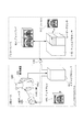
(第1の実施形態)
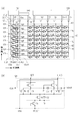
先ず、図1(a),(b)を用いて本発明の第1の実施形態に係る検出装置について説明する。図1(a)は検出装置の概略的等価回路であり、図1(b)は検出装置の駆動回路部に設けられる単位回路を説明する概略的等価回路である。
(First embodiment)
First, the detection apparatus according to the first embodiment of the present invention will be described with reference to FIGS. FIG. 1A is a schematic equivalent circuit of the detection device, and FIG. 1B is a schematic equivalent circuit illustrating a unit circuit provided in a drive circuit unit of the detection device.
本発明の検出装置100は、図1(a)に示すように、画素110が絶縁性基板101の上に行列状に複数配置された画素アレイを含む。本実施形態では、m行n列の画素アレイである。この画素110は、放射線又は光を電荷に変換する変換素子111と、変換された電荷に応じた電気信号を出力するスイッチ素子112と、を含む。変換素子111の第1電極には、スイッチ素子112のソース及びドレインの一方が電気的に接続され、変換素子111の第2電極には、電極配線180に電気的に接続される。電極配線180は、接続用端子Vsを介して電源部140に接続される。スイッチ素子112のソース及びドレインの他方には、信号配線170が電気的に接続される。信号配線170は、行方向に複数(n本)配置され、各々が列毎に、列方向に配列された複数のスイッチ素子112のソース及びドレインの他方に共通に接続され、接続用端子S1−Snを介して外部の読出回路部130に接続される。スイッチ素子103の制御電極には、駆動配線160が電気的に接続される。駆動配線160は、列方向に複数(m本)配置され、各々が行毎に、行方向に配列された複数のスイッチ素子112のゲートに共通に接続し、また、絶縁性基板101の上に設けられた駆動回路部120に接続される。駆動回路部120は、接続端子Vssを介して電源部140と接続され、接続端子CL1,CL2,ST,LHを介して制御部150と接続される。電源部140は、変換素子に供給するための電圧Vsを電極配線180に供給し、スイッチ素子の非導通電圧VSSを駆動回路部120に供給する。制御部150は、駆動回路部120が駆動配線160へのスイッチ素子112の導通電圧VDDの供給を開始するためのスタート信号ΦSTを駆動回路部120に供給する。また、制御部150は、導通電圧VDD又は非導通電圧VSSの供給のタイミングを規定するクロック信号ΦCL1及びΦCL2を駆動回路部120に供給する。更に、制御部150は、駆動配線160への導通電圧VDDの供給を終了するためのリセット信号と、駆動配線160への非導通電圧VSSの供給を維持するための制御信号ΦLHと、を駆動回路部120に供給する。なお、本実施形態では、制御信号ΦLHがリセット信号を兼ねるものとなっている。
As shown in FIG. 1A, the
駆動回路部120は、絶縁性基板101の上に設けられた単位回路121を一つの駆動配線160に一つ備えており、駆動回路部120全体としては、複数の駆動配線160夫々に対をなして複数個(m個)の単位回路121を備えている。単位回路121は、導通電圧VDDと非導通電圧VSSとを含む出力信号Vgを駆動配線160に供給する。
The
単位回路121は、図1(b)に示すように、出力部VOUTと、第1入力部SETと、第2入力部CLKと、第3入力部VSSと、第4入力部RESETと、第5入力部LHLDを含む。ここで、第1入力部SETは、スタート信号ΦST又は前段の単位回路の出力信号Vgが入力される部分であり、出力部VOUTは、出力信号Vgを駆動配線160に供給するために駆動配線160に接続される部分である。なお、本発明において、スタート信号ΦSTと前段の単位回路の出力信号Vgを、単位回路121がスイッチ素子112の導通電圧VDDの供給を開始するために単位回路121に入力される開始信号と規定する。また、第2入力部CLKは、クロック信号ΦCL1又はΦCL2が入力される部分であり、第3入力部VSSは、非導通電圧VSSが入力される部分である。また、第4入力部RESETは、リセット信号又は後段の単位回路121の出力信号Vgが入力される部分であり、第5入力部LHLDは、制御信号ΦLHは入力される部分である。なお、本発明において、リセット信号と後段の単位回路121の出力信号Vgを、単位回路121がスイッチ素子112の導通電圧VDDの供給を終了するために単位回路121に入力される終了信号と規定する。
As shown in FIG. 1B, the
単位回路121は、第1回路と第2回路に加えて、第3回路を有することを特徴とする。
The
第1回路は、第1薄膜トランジスタT1と第2薄膜トランジスタT2と第1容量素子C1とを含む。この第1回路は、ある単位回路121が選択された際に第2入力部CLKに入力されるクロック信号ΦCLの最大値であるVDDに基づいて導通電圧としてVDDを出力部VOUTに供給する回路である。第1容量素子C1は、一方の端子が出力部VOUTに接続される。第1薄膜トランジスタT1は、第1入力部SETと第1容量素子C1の他方の端子との間で第1容量素子C1に直列に接続される。第1薄膜トランジスタT1は、そのソース及びドレインの一方とゲートが第1入力部SETに接続され、ソース及びドレインの他方が第1容量素子C1の他方の端子に第1節点Pで接続される。また、第2薄膜トランジスタT2は、第2入力部CLKと出力部OUTとの間に設けられる。第2薄膜トランジスタT2は、そのゲートが第1節点Pと接続され、ソース及びドレインの一方が第2入力部CLKと接続され、ソース及びドレインの他方が出力部VOUTと接続される。
The first circuit includes a first thin film transistor T1, a second thin film transistor T2, and a first capacitor element C1. The first circuit supplies V DD to the output unit VOUT as a conduction voltage based on V DD which is the maximum value of the clock signal ΦCL input to the second input unit CLK when a
第2回路は、第3薄膜トランジスタT3と第4薄膜トランジスタT4と第2容量素子C2と第5薄膜トランジスタT5と第6薄膜トランジスタT6とを含む。この第2回路は、駆動配線160への導通電圧VDDの供給を終了するためにリセット信号又は後段の単位回路121の出力信号Vgに応じて、非導通電圧VSSの駆動配線160への供給を行う回路である。第3薄膜トランジスタT3は、第3入力部VSSと第1容量素子C1の他方の端子との間で第1容量素子C1と直列に接続される。第3薄膜トランジスタT3は、そのゲートが第4入力部RESETと接続され、ソース及びドレインの一方が第3入力部VSSに接続されソース及びドレインの他方が第1容量素子C1の他方の端子に第1節点Pで接続される。第4薄膜トランジスタT4は、第3入力部VSSと出力部VOUTとの間に設けられる。第4薄膜トランジスタT4は、そのゲートが第4入力部RESETに接続され、ソース及びドレインの一方が第3入力部VSSに接続され、ソース及びドレインの他方が出力部VOUTに接続される。第2容量素子C2は、第3入力部VSSと第4薄膜トランジスタT4のゲートとの間に設けられる。第2容量素子C2は、その一方の端子が第3入力部VSSに接続され、他方の端子が第4薄膜トランジスタT4のゲートに第2節点Qで接続される。第5薄膜トランジスタT5は、第4入力部RESETと第3薄膜トランジスタT3のゲート及び第4薄膜トランジスタT4のゲートとの間に設けられる。第5薄膜トランジスタT5は、そのソース及びドレインの一方とゲートが第4入力部RESETに接続され、ソース及びドレインの他方が第2節点Qに接続される。第6薄膜トランジスタT6は、第2容量素子に並列に設けられる。第6薄膜トランジスタT6は、そのゲートが第1入力部SETに接続され、ソース及びドレインの一方が第3入力部VSSに接続され、ソース及びドレインの他方が第2節点Qに接続される。
The second circuit includes a third thin film transistor T3, a fourth thin film transistor T4, a second capacitive element C2, a fifth thin film transistor T5, and a sixth thin film transistor T6. This second circuit supplies the non-conduction voltage VSS to the
そして、第3回路は、少なくとも第7薄膜トランジスタT7を含む。この第3回路は、制御信号ΦLHの電圧VDDに応じて駆動配線160への非導通電圧VSSの供給を維持する回路である。ここで、本発明では、制御信号ΦLHの電圧VDDを制御電圧と称する。第7薄膜トランジスタT7は、制御信号ΦLHの電圧VDDに応じて出力部VOUTへの非導通電圧VSSの供給を維持するために、第3入力部VSSと第5入力部LHLDと出力部VOUTとの間に設けられる。第7薄膜トランジスタT7は、そのゲートが第5入力部LHLDに接続され、ソース及びドレインの一方が第3入力部VSSに接続され、ソース及びドレインの他方が出力部VOUTに接続される。制御部150から複数の単位回路121の第7薄膜トランジスタT7に共通に制御信号ΦLHの電圧VDDが供給されることにより、供給された単位回路121に接続された駆動配線160への非導通電圧VSSの供給が維持される。なお、本実施形態の第3回路は、第7薄膜トランジスタT7に加えて、第8薄膜トランジスタT8も含むものである。第8薄膜トランジスタT8は、制御信号ΦLHに応じて第1節点Pを非導通電圧VSSに維持するために、第3入力部VSSと第5入力部LHLDと第1節点Pとの間に設けられる。第8薄膜トランジスタT8は、そのゲートが第5入力部LHLDに接続され、ソース及びドレインの一方が第3入力部VSSに接続され、ソース及びドレインの他方が第1節点Pに接続される。制御部150から複数の単位回路121の第8薄膜トランジスタT8に共通に制御信号ΦLHの電圧VDDが供給されることにより、供給された単位回路121の第1節点Pへの非導通電圧VSSの供給が維持される。なお、本実施形態では制御電圧として制御信号ΦLHの電圧VDDを用いたが、本発明はそれに限定されるものではない。制御電圧として制御信号ΦLHの電圧VSSを用いてもよく、その場合には、制御部150と第5入力部150との間に極性反転回路を設ける等、適宜設計し得る。
The third circuit includes at least a seventh thin film transistor T7. The third circuit is a circuit for maintaining the supply of non-conducting voltage V SS to the driving
本発明の駆動回路部120を構成する各薄膜トランジスタは、非晶質シリコン等の非晶質半導体材料、多結晶シリコン等の多結晶半導体材料、有機半導体材料、酸化物半導体材料を用いることができる。ここで、例えば、スイッチ素子112としてトップゲート型の多結晶シリコンのTFTを用いる場合、駆動回路部120もトップゲート型の多結晶シリコンのTFTを用いることが好ましい。また、スイッチ素子112としてボトムゲート型の非晶質シリコンのTFTを用いた場合であっても、駆動回路部120ではトップゲート型の多結晶シリコンのTFTを用いてもよい。
For each thin film transistor included in the
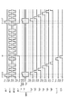
次に、図2のタイミングチャートを用いて、図1(a)及び図1(b)に示す検出装置の動作を説明する。なお、ここでは、各薄膜トランジスタT1〜T8の閾値電圧をいずれもVthとする。また、スタート信号ΦST、クロック信号ΦCL1及びΦCL2、及び、制御信号ΦLHの最大電圧値をVDDと、最小電圧値をVSSと、する。また、クロック信号ΦCL1とΦCL2とは、位相が互いに180度ことなるものであり、ΦCL1は奇数行の単位回路121に、ΦCL2は偶数行の単位回路121に、それぞれ供給されるものである。また、導通電圧VDDと非導通電圧VSSと閾値電圧Vthは、|VDD−VSS|>Vth、且つ、VDD>2Vth、を満たすように設定する
時刻t1では、1段目の単位回路121の第1入力部SETにスタート信号ΦSTのVDDが、第2入力部CLKにクロック信号ΦCL1のVSSが、第5入力部LHLDに制御信号ΦLHのVSSが、制御部150から与えられる。また、1段目の単位回路121の第3入力部VSSにはVSSが電源部140から与えられており、第4入力部RESETには2段目の出力信号Vg2としてVSSが与えられている。これにより、1段目の単位回路121では、第1薄膜トランジスタT1と第6薄膜トランジスタT6が導通状態となる。そして、1段目の単位回路121では、第3薄膜トランジスタT3と第4薄膜トランジスタT4と第5薄膜トランジスタT5と第7薄膜トランジスタT7と第8薄膜トランジスタT8とが非導通状態となる。これにより、1段目の単位回路121では、第1節点Pの電位が|VDD−Vth|となり、第2節点Qの電位がVSSとなる。そのため、1段目の単位回路121では、第2薄膜トランジスタT2が導通状態となり、出力部VOUTの電位がVSSとなる。
Next, the operation of the detection apparatus shown in FIGS. 1A and 1B will be described using the timing chart of FIG. Here, the threshold voltages of the thin film transistors T1 to T8 are all set to Vth. Further, the start signal .phi.ST, the clock signal ΦCL1 and CL2, and the maximum voltage value of the control signal ΦLH and V DD, and V SS the minimum voltage value is. The clock signals ΦCL1 and ΦCL2 are 180 degrees out of phase with each other. ΦCL1 is supplied to the odd-numbered
次に、時刻t2では、1段目の単位回路121の第1入力部SETにスタート信号ΦSTのVSSが、第2入力部CLKにクロック信号ΦCL1のVDDが、第5入力部LHLDに制御信号ΦLHのVSSが、制御部150から与えられる。また、1段目の単位回路121の第3入力部VSSにはVSSが電源部140から与えられており、第4入力部RESETには2段目の出力信号Vg2のVSSが与えられている。それにより、1段目の単位回路121では、第2薄膜トランジスタT2以外の薄膜トランジスタが非導通状態となる。この際、第2薄膜トランジスタT2のソース及びドレインの他方とゲートとが第1容量素子C1を介して結合しているため、1段目の単位回路121では、第1節点Pの電位が|2VDD−Vth|となる。それにより、1段目の単位回路121では、出力部VOUTの電位がVDDとなる(ブートストラップ動作)。これにより、1行目の駆動配線160に出力信号Vg1としてVDDが1段目の単位回路121から供給され、1行目の複数のスイッチ素子112が導通状態となる。これにより、1行目の複数の変換素子111の電荷に応じた電気信号が、行方向に配列された複数の信号配線170に並列に出力される。一方、2段目の単位回路121の第1入力部SETに1段目の単位回路121の出力信号Vg1のVDDが、第2入力部CLKにクロック信号ΦCL2のVSSが、第5入力部LHLDに制御信号ΦLHのVSSが、制御部150から与えられる。また、2段目の単位回路121の第3入力部VSSにはVSSが電源部140から与えられており、第4入力部RESETには3段目の出力信号Vg3のVSSが与えられている。そのため、時刻t1の1段目の単位回路121と同様に、2段目の単位回路121では、第1節点Pの電位が|VDD−Vth|となり、第2節点Qの電位がVSSとなり、第2薄膜トランジスタT2が導通状態となり、出力部VOUTの電位がVSSとなる。
Next, at time t2, the V SS of the start signal ΦST is controlled by the first input unit SET of the
次に、時刻t3では、1段目の単位回路121の第1入力部SETにスタート信号ΦSTのVSSが、第2入力部CLKにクロック信号ΦCL1のVSSが、第5入力部LHLDに制御信号ΦLHのVSSが、制御部150から与えられる。また、1段目の単位回路121の第3入力部VSSにはVSSが電源部140から与えられており、第4入力部RESETには後述する2段目の出力信号Vg2のVDDが与えられる。それにより、1段目の単位回路121では、第1薄膜トランジスタT1と第6薄膜トランジスタT6と第7薄膜トランジスタT7と第8薄膜トランジスタT8とが非導通状態である。そして、1段目の単位回路121では、第5薄膜トランジスタT5が導通状態となる。これにより、1段目の単位回路121では、第1節点Pの電位がVSSとなり、第2節点Qの電位が|VDD−Vth|となる。そのため、1段目の単位回路121では、第2薄膜トランジスタT2が非導通状態となり、第3薄膜トランジスタT3と第4薄膜トランジスタT4とが導通状態となり、出力部VOUTの電位がVSSとなる。一方、2段目の単位回路121の第1入力部SETに1段目の単位回路121の出力信号Vg1のVSSが、第2入力部CLKにクロック信号ΦCL2のVDDが、第5入力部LHLDに制御信号ΦLHのVSSが、制御部150から与えられる。また、2段目の単位回路121の第3入力部VSSにはVSSが電源部140から与えられており、第4入力部RESETには3段目の出力信号Vg3のVSSが与えられている。そのため、時刻t2の1段目の単位回路121と同様に、2段目の単位回路121では、第1節点Pの電位が|2VDD−Vth|となり、出力部VOUTの電位がVDDとなる(ブートストラップ動作)。つまり、2段目(後段)の単位回路121は、1段目(前段)の単位回路121の出力信号Vg1のVDDを引き金として、1段目(前段)からクロック信号の半周期分の時間(t3−t2)遅れて、1段目(前段)と同様の動作を行う。このような動作がm段目の単位回路121まで順次行われ、列方向に配置された複数の駆動配線160には、導通電圧VDDが駆動回路部120から順次に供給される。
Next, at time t3, V SS start signal ΦST to a first input SET of the
次に、時刻t4では、m段目の単位回路121の第1入力部SETにm−1段目の単位回路121の出力信号Vg1のVSSが、第2入力部CLKにクロック信号ΦCL1のVSSが、制御部150から与えられる。また、1段目の単位回路121の第4入力部RESETと第5入力部LHLDに制御信号ΦLHのVDDが、制御部150から与えられる。そして、1段目の単位回路121の第3入力部VSSにはVSSが電源部140から与えられている。それにより、m段目の単位回路121では、第1薄膜トランジスタT1と第6薄膜トランジスタT6とが非導通状態である。そして、m段目の単位回路121では、第5薄膜トランジスタT5と第7薄膜トランジスタT7と第8薄膜トランジスタT8とが導通状態となる。これにより、m段目の単位回路121では、第1節点Pの電位がVSSとなり、第2節点Qの電位が|VDD−Vth|となり、出力部VOUTの電位がVSSとなる。そのため、m段目の単位回路121では、第2薄膜トランジスタT2が非導通状態となり、第3薄膜トランジスタT3と第4薄膜トランジスタT4とが導通状態となり、出力部VOUTの電位がVSSとなる。また、他の単位回路121の第5入力部LHLDにも、制御信号ΦLHのVDDが、制御部150から共通に与えられる。これにより、他の単位回路121でも、第7薄膜トランジスタT7と第8薄膜トランジスタT8とが導通状態となる。それにより、他の単位回路121でも、第1節点Pの電位がVSSとなり、出力部VOUTの電位がVSSとなる。
Next, at time t4, V SS of the output signal Vg1 of the m−1
次に、時刻t5では、制御信号ΦLHがVDDからVSSとなり、各単位回路121の第7薄膜トランジスタT7及び第8薄膜トランジスタT8は非導通状態となる。そして、時刻t1と同様に、1段目の単位回路121の第1入力部SETにスタート信号ΦSTのVDDが、第2入力部CLKにクロック信号ΦCL1のVSSが、制御部150から与えられる。また、1段目の単位回路121の第3入力部VSSにはVSSが電源部140から与えられており、第4入力部RESETには2段目の出力信号Vg2としてVSSが与えられている。これにより、時刻t1と同様に、1段目の単位回路121では、第1節点Pの電位が|VDD−Vth|となり、第2節点Qの電位がVSSとなる。そのため、1段目の単位回路121では、第2薄膜トランジスタT2が導通状態となり、出力部VOUTの電位がVSSとなる。そして時刻t6では、時刻t2と同様に、1段目の単位回路121では出力部VOUTの電位がVDDとなり、時刻t7では、時刻t3と同様に、2段目の単位回路121では出力部VOUTの電位がVDDとなる。
Next, at time t5, the control signal ΦLH changes from V DD to V SS , and the seventh thin film transistor T7 and the eighth thin film transistor T8 of each
ここで、制御信号ΦLHは、時刻t4から時刻t5までVDDとなっており、その間は制御信号ΦLHが与えられている全ての単位回路121において出力部VOUTの電位がVSSに維持される。そのため、単位回路121は、制御信号ΦLHがVDDとなっていることに応じて、駆動配線160への非導通電圧VSSの供給を維持する。第5薄膜トランジスタT5や第6薄膜トランジスタT6にチャネルリークがあると、時間経過によっては第4薄膜トランジスタT4のゲートにVth以上の電圧供給が維持できなくなる。それにより、第4薄膜トランジスタT4によって出力部VOUTの電位をVSSに維持できなくなる。特に検出装置では、時刻t4から時刻t5までの間に、放射線又は光が照射される必要があり、その時間は一般撮影(静止画撮影)では1〜3秒必要となる。検出装置では、少なくともその間はスイッチ素子112を非導通状態とし続けなければならないため、1〜3秒もの長時間にわたって出力部VOUTの電位を非導通電圧VSSに維持しなければならない。出力部VOUTがフローティング状態となると、第2入力部CLKに入力されるクロック信号ΦCLの電位変動が、駆動配線160に影響し、駆動配線160の電位が変動する。駆動配線160と信号配線170とが交差する領域の寄生容量を介して駆動配線160の電位変動信号配線170の電位に影響を与え、画素から出力される信号に駆動配線160の電位変動が混入する。本発明では、第4薄膜トランジスタT4によって出力部VOUTの電位をVSSに維持できない場合でも、制御信号ΦLHのVDDが供給され続ける第7薄膜トランジスタT7によって出力部VOUTへの非導通電圧VSSの供給を維持できる。それにより、駆動配線160の電位変動に起因するS/N比の低下を抑制することが可能な検出装置を提供できる。
Here, the control signal ΦLH is a V DD from time t4 to time t5, during which the potential of the output unit VOUT is maintained at V SS in all the
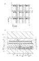
次に、図3(a)及び図3(b)を用いて、本発明の第1の実施形態に係る検出装置の一画素の構成について説明する。図3(a)は平面図であり、図3(b)は図3(a)のA−A’での断面図である。 Next, the configuration of one pixel of the detection apparatus according to the first embodiment of the present invention will be described with reference to FIGS. 3 (a) and 3 (b). FIG. 3A is a plan view, and FIG. 3B is a cross-sectional view taken along the line A-A ′ of FIG.
本実施形態では、スイッチ素子112にトップゲート型でダブルゲート型の多結晶シリコンTFTを用いている。スイッチ素子112は、絶縁性基板101の上に、真性半導体領域301と第1導電型の不純物半導体領域302とを含む多結晶シリコン層と、第1絶縁層303と、第1導電層304と、が絶縁性基板101側から順に積層された構成である。真性半導体領域301はTFTのチャネルとして、不純物半導体領域302はソース又はドレインとして、第1絶縁層303はゲート絶縁層として、第1導電層304はゲート又は駆動配線160として、それぞれ機能する。スイッチ素子112は第2絶縁層305によって覆われる。この第2絶縁層305はスイッチ素子112のパッシベーション層として機能する。第2絶縁層305上に設けられた第2導電層306は、第2絶縁層305及び第1絶縁層303に設けられたコンタクトホールにおいて不純物半導体領域302と接続される。ソース及びドレインの一方である不純物半導体領域302と接続された第2導電層306は変換素子110との接続端子として機能し、ソース及びドレインの他方である不純物半導体領域302と接続された第2導電層306は、信号配線170として機能する。第2導電層306は第3絶縁層307によって覆われる。この第3絶縁層307はスイッチ素子112及び信号配線170のパッシベーション層として機能する。第3絶縁層307は第4絶縁層308によって覆われる。この第4絶縁層308は、有機絶縁材料からなり、大きな膜厚で準備することにより、平坦化層として機能する。第4絶縁層309の上には、変換素子111が設けられる。本実施形態では、変換素子111として、放射線を光に変換するシンチレータ317と、その光を電荷に変換する光電変換素子と、を含むものを用いている。光電変換素子は、第3導電層310と、第1導電型の不純物半導体層311と、真性半導体層312と、第2導電型の不純物半導体層313と、第4導電層314と、が絶縁性基板101側から順に積層された構成である。第3導電層310は変換素子111の第1電極として機能し、第3絶縁層307及び第4絶縁層308に設けられたコンタクトホール309において第2導電層306と接続される。第1導電型の不純物半導体層311と真性半導体層312と第2導電型の不純物半導体層313には非晶質シリコンが用いられる。第4導電層314は変換素子111の第2電極として機能し、電極配線180として機能する第5導電層315と接続される。光電変換素子及び電極配線180は第5絶縁層316によって覆われ、第5絶縁層316の上にシンチレータ317が配置される。
In this embodiment, a top gate type double gate type polycrystalline silicon TFT is used for the
ここで、本実施形態では、変換素子111として、放射線を光に変換するシンチレータと、その光を電荷に変換する光電変換素子と、を含む間接型変換素子を用いたが、本発明はそれに限定されるものではない。変換素子111として、放射線を直接電荷に変換する直接型変換素子を用いてもよい。また、スイッチ素子112として、多結晶シリコンTFTを用いたが、本発明はそれに限定されるものではない。非晶質シリコンTFTや酸化物半導体を用いた酸化物TFT、有機半導体を用いた有機TFTも用いることができる。ここで、半導体材料としてシリコンを用いたが、本発明はこれに限定されるものではなく、ゲルマニウム等の他の半導体材料を用いてもよい。
Here, in this embodiment, as the
なお、本実施形態では、第3回路に、ゲートが第5入力部LHLDに接続され、ソース及びドレインの一方が第3入力部VSSに接続され、ソース及びドレインの他方が出力部VOUTに接続される第7薄膜トランジスタT7を用いた。しかしながら本発明はそれに限定されるものではない。図4に示すように、図1(b)の第7薄膜トランジスタT7に替えて、第7薄膜トランジスタT7’を用いてもよい。この第7薄膜トランジスタT7’は、そのゲートとソース及びドレインの一方とが第5入力部LHLDに接続され、そのソース及びドレインの他方が第2節点Qに接続される。それにより、第4薄膜トランジスタT4のゲートへのVth以上の電圧供給が維持され、第4薄膜トランジスタT4による出力部VOUTへの非導通電圧VSSの供給が維持される。つまり、本実施形態においては、第4薄膜トランジスタT4は第2回路だけでなく第3回路にも属するものである。同様に、第3薄膜トランジスタT3のゲートへのVth以上の電圧供給が維持され、第3薄膜トランジスタT3による第1節点Pへの非導通電圧VSSの供給が維持される。つまり、第3薄膜トランジスタT3も、第2回路だけでなく第3回路にも属するものである。 In this embodiment, in the third circuit, the gate is connected to the fifth input unit LHLD, one of the source and the drain is connected to the third input unit VSS, and the other of the source and the drain is connected to the output unit VOUT. A seventh thin film transistor T7 was used. However, the present invention is not limited thereto. As shown in FIG. 4, a seventh thin film transistor T7 ′ may be used instead of the seventh thin film transistor T7 of FIG. The seventh thin film transistor T7 ′ has a gate and one of a source and a drain connected to the fifth input portion LHLD, and the other of the source and the drain connected to the second node Q. Thereby, Vth or more voltage supply to the gate of the fourth thin film transistor T4 is maintained, the supply of the non-conducting voltage V SS to the output unit VOUT of the fourth thin film transistor T4 is maintained. That is, in the present embodiment, the fourth thin film transistor T4 belongs to not only the second circuit but also the third circuit. Similarly, Vth or more voltage supply to the gate of the third thin film transistor T3 is maintained, the supply of the non-conducting voltage V SS to the first node P according to the third thin film transistor T3 is maintained. That is, the third thin film transistor T3 belongs to the third circuit as well as the second circuit.
(第2の実施形態)
次に、図5(a),(b)を用いて本発明の第2の実施形態に係る検出装置について説明する。図5(a)は検出装置の概略的等価回路であり、図5(b)は検出装置の駆動回路部に設けられる単位回路を説明する概略的等価回路である。なお、第1の実施形態で説明したものと同じものは同じ番号を付与し、詳細な説明は割愛する。
(Second Embodiment)
Next, a detection apparatus according to a second embodiment of the present invention will be described with reference to FIGS. FIG. 5A is a schematic equivalent circuit of the detection device, and FIG. 5B is a schematic equivalent circuit illustrating a unit circuit provided in a drive circuit unit of the detection device. In addition, the same thing as what was demonstrated in 1st Embodiment is provided with the same number, and detailed description is omitted.
本実施形態における駆動回路部120’は、複数の単位回路121を一組とする単位回路群を複数含む。図5(a)では、3段分の単位回路を一組とする単位回路群をX群含むものである。そして、制御部150’は、複数の単位回路群毎に制御信号ΦLH1〜ΦLHxをそれぞれ独立に供給できるように、構成されている。これにより、駆動配線160への非導通電圧VSSの供給の維持を、単位回路群毎に別々に制御することが可能となる。また、制御部150’は、複数の単位回路群毎にスタート信号ΦST1に加えて、選択信号ΦST2〜ΦSTxをそれぞれ独立に供給できるように、構成されている。これにより、複数の単位回路群の中からある単位回路群を選択し、選択された単位回路群から駆動配線160への導通電圧の供給を開始することが可能となる。更に、本実施形態では、1段目の単位回路121を除く、単位回路群の初段の単位回路には、単位回路121に替えて、図5(b)に示す単位回路122を用いる。この単位回路122は、単位回路121の構成要素に加えて、更に、第6入力部TSETと、第4回路と、を含む。この第4回路は、選択信号ΦST2〜ΦSTxに応じて、第1回路に導通電圧VDDを駆動配線160に供給させる回路であり、第9薄膜トランジスタT9と、第10薄膜トランジスタT10と、を含む。第9薄膜トランジスタT9は、第6入力部TSETと第1容量素子C1の他方の端子との間で第1容量素子C1に直列に接続される。第9薄膜トランジスタT9は、そのソース及びドレインの一方とゲートが第6入力部TSETに接続され、ソース及びドレインの他方が第1節点Pに接続される。第10薄膜トランジスタT10は、第2容量素子C2及び第6薄膜トランジスタT6に並列に設けられる。第10薄膜トランジスタT10は、そのゲートが第6入力部TSETに接続され、ソース及びドレインの一方が第3入力部VSSに接続され、ソース及びドレインの他方は第2節点Qに接続される。
The
次に、図6のタイミングチャートを用いて、図5(a)及び図5(b)に示す検出装置の動作を説明する。なお、ここでは、第1群の単位回路群と第X群の単位回路群の単位回路を動作させず、第2群の単位回路群の初段(4段目)の単位回路122から動作を開始する例を用いて説明する。なお、第1の実施形態で説明したものと同じものは同じ番号を付与し、詳細な説明は割愛する。
Next, the operation of the detection apparatus shown in FIGS. 5A and 5B will be described using the timing chart of FIG. Here, the unit circuit of the first group and the unit circuit group of the X group are not operated, and the operation starts from the
時刻t1では、1段目の単位回路121の第1入力部SETにスタート信号ΦST1のVSSが、第2入力部CLKにクロック信号ΦCL1のVSSが、制御部150’から与えられる。そして、第1群の全ての単位回路121の第5入力部LHLDに制御信号ΦLH1のVDDが制御部150’から与えられる。また、第X群の初段であるm−2段目の単位回路121の第1入力部SETに選択信号ΦSTxのVSSが、第2入力部CLKにクロック信号ΦCL1のVSSが、制御部150’から与えられる。そして、第X群の全ての単位回路121及び122の第5入力部LHLDに制御信号ΦLHxのVDDが制御部150’から与えられる。これにより、第1群及び第X群の全ての単位回路121及び122の出力部VOUTの電位がVSSとなる。この制御信号ΦLH1及びΦLHxは、後述する時刻t5までVDDが維持され、第1群及び第X群の全ての単位回路121及び122の出力部VOUTの電位がt5までVSSに維持される。つまり、複数の単位回路群のうち選択的に導通電圧が供給されるべき複数の駆動配線160に接続される単位回路121を含む単位回路群を除く単位回路群(第1群及び第X群)の単位回路121及び122の出力部が非導通電圧に維持される。一方、第2群の初段である4段目の単位回路122の第1入力部SETに3段目の出力信号Vg3のVSSが、第2入力部CLKにクロック信号ΦCL2のVDDが、第5入力部LHLDに制御信号ΦLHのVSSが、制御部150’から与えられる。また、4段目の単位回路122の第3入力部VSSにはVSSが電源部140から与えられており、第4入力部RESETには5段目の出力信号Vg5のVSSが与えられている。更に、第6入力部TSETには選択信号ΦST2のVDDが制御部150’から与えられる。これにより、4段目の単位回路122では、第9薄膜トランジスタT9と第10薄膜トランジスタT10が導通状態となる。そして、4段目の単位回路122では、第1薄膜トランジスタT1から第8薄膜トランジスタT8までが非導通状態となる。これにより、4段目の単位回路122では、第1節点Pの電位が|VDD−Vth|となり、第2節点Qの電位がVSSとなる。そのため、4段目の単位回路122では、第2薄膜トランジスタT2が導通状態となり、出力部VOUTの電位がVSSとなる。
At time t1, V SS start signal ΦST1 to a first input SET of the
次に、時刻t2では、4段目の単位回路122の第1入力部SETに3段目の出力信号Vg3のVSSが、第2入力部CLKにクロック信号ΦCL2のVDDが、第5入力部LHLDに制御信号ΦLH2のVSSが、制御部150’から与えられる。また、4段目の単位回路122の第3入力部VSSにはVSSが電源部140から与えられており、第4入力部RESETには2段目の出力信号Vg2のVSSが与えられている。更に、第6入力部TSETには選択信号ΦST2のVSSが制御部150’から与えられる。それにより、4段目の単位回路122では、第2薄膜トランジスタT2以外の薄膜トランジスタが非導通状態となる。この際、第2薄膜トランジスタT2のソース及びドレインの他方とゲートとが第1容量素子C1を介して結合しているため、4段目の単位回路122では、第1節点Pの電位が|2VDD−Vth|となる。それにより、4段目の単位回路122では、出力部VOUTの電位がVDDとなる(ブートストラップ動作)。これにより、4行目の駆動配線160に出力信号Vg4としてVDDが4段目の単位回路122から供給され、4行目の複数のスイッチ素子112が導通状態となる。これにより、4行目の複数の変換素子111の電荷に応じた電気信号が、行方向に配列された複数の信号配線170に並列に出力される。一方、5段目の単位回路121の第1入力部SETに4段目の単位回路122の出力信号Vg4のVDDが、第2入力部CLKにクロック信号ΦCL1のVSSが、第5入力部LHLDに制御信号ΦLH2のVSSが、制御部150’から与えられる。また、5段目の単位回路121の第3入力部VSSにはVSSが電源部140から与えられており、第4入力部RESETには6段目の出力信号Vg6のVSSが与えられている。そのため、時刻t1の4段目の単位回路122と同様に、5段目の単位回路121では、第1節点Pの電位が|VDD−Vth|となり、第2節点Qの電位がVSSとなり、第2薄膜トランジスタT2が導通状態となり、出力部VOUTの電位がVSSとなる。
Next, at time t2, V SS of the third stage output signal Vg3 is input to the first input section SET of the fourth
次に、時刻t3では、4段目の単位回路122の第1入力部SETに3段目の出力信号Vg3のVSSが、第2入力部CLKにクロック信号ΦCL2のVSSが、第5入力部LHLDに制御信号ΦLH2のVSSが、制御部150’から与えられる。また、4段目の単位回路122の第3入力部VSSにはVSSが電源部140から与えられており、第4入力部RESETには後述する5段目の出力信号Vg2のVDDが与えられる。更に、第6入力部TSETには選択信号ΦST2のVSSが制御部150’から与えられる。それにより、4段目の単位回路122では、第1薄膜トランジスタT1と第6薄膜トランジスタT6から第10薄膜トランジスタT10までが非導通状態である。そして、4段目の単位回路122では、第5薄膜トランジスタT5が導通状態となる。これにより、4段目の単位回路122では、第1節点Pの電位がVSSとなり、第2節点Qの電位が|VDD−Vth|となる。そのため、4段目の単位回路122では、第2薄膜トランジスタT2が非導通状態となり、第3薄膜トランジスタT3と第4薄膜トランジスタT4とが導通状態となり、出力部VOUTの電位がVSSとなる。一方、5段目の単位回路121の第1入力部SETに1段目の単位回路121の出力信号Vg4のVSSが、第2入力部CLKにクロック信号ΦCL1のVDDが、第5入力部LHLDに制御信号ΦLH2のVSSが、制御部150’から与えられる。また、5段目の単位回路121の第3入力部VSSにはVSSが電源部140から与えられており、第4入力部RESETには6段目の出力信号Vg6のVSSが与えられている。そのため、時刻t2の4段目の単位回路122と同様に、5段目の単位回路121では、第1節点Pの電位が|2VDD−Vth|となり、出力部VOUTの電位がVDDとなる(ブートストラップ動作)。つまり、5段目(後段)の単位回路121は、4段目(前段)の単位回路122の出力信号Vg4のVDDを引き金として、4段目(前段)からクロック信号の半周期分の時間(t3−t2)遅れて、4段目(前段)と同様の動作を行う。このような動作がm−3段目の単位回路121まで順次行われ、列方向に配置された複数の駆動配線160のうちm−3行目の駆動配線160までは、導通電圧VDDが駆動回路部120から順次に供給される。
Next, at time t3, V SS of the first input unit 3-stage output signal SET Vg3 of the
次に、時刻t4では、第2群の全ての単位回路121及び122の第5入力部LHLDに制御信号ΦLH2のVDDが制御部150’から与えられる。これにより、第2群の全ての単位回路121及び122の出力部VOUTの電位がVSSとなる。この制御信号ΦLH2は、時刻t5までVDDが維持され、第2群の全ての単位回路121及び122の出力部VOUTの電位がt5までVSSに維持される。
Next, at time t4, V DD of the control signal ΦLH2 is supplied from the
時刻t5以降の動作については、第1群の初段の単位回路121を除く他の群の初段の単位回路122の第5入力部LHLDに制御信号ΦLH2〜ΦLHxのVSSが制御部150’から与えられること以外は、第1の実施形態と同様である。そのため、詳細な説明は割愛する。
Regarding the operation after time t5, the V SS of the control signals ΦLH2 to ΦLHx is given from the
これにより、本実施形態では、複数の単位回路群の中から選択して単位回路群を動作させることが可能となる。更に、複数の単位回路群の中から選択して単位回路群を動作させた場合でも、駆動配線160の電位変動に起因するS/N比の低下を抑制することが可能な検出装置を提供できる。
Thereby, in this embodiment, it becomes possible to select and operate the unit circuit group from among the plurality of unit circuit groups. Furthermore, it is possible to provide a detection device capable of suppressing a decrease in the S / N ratio due to potential fluctuation of the
なお、本実施形態では、第3回路に、ゲートが第5入力部LHLDに接続され、ソース及びドレインの一方が第3入力部VSSに接続され、ソース及びドレインの他方が出力部VOUTに接続される第7薄膜トランジスタT7を用いた。しかしながら、第1の実施形態と同様に、図7に示すように、図5(b)の第7薄膜トランジスタT7に替えて、第7薄膜トランジスタT7’を用いてもよい。 In this embodiment, in the third circuit, the gate is connected to the fifth input unit LHLD, one of the source and the drain is connected to the third input unit VSS, and the other of the source and the drain is connected to the output unit VOUT. A seventh thin film transistor T7 was used. However, as in the first embodiment, as shown in FIG. 7, a seventh thin film transistor T7 'may be used instead of the seventh thin film transistor T7 in FIG.
(応用実施形態)
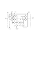
次に、図7を用いて、本発明の検出装置を用いた放射線検出システムを説明する。
(Application embodiment)
Next, a radiation detection system using the detection apparatus of the present invention will be described with reference to FIG.
放射線源であるX線チューブ6050で発生したX線6060は、患者あるいは被験者6061の胸部6062を透過し、放射線検出装置6040に含まれる変換部3の各変換素子12に入射する。この入射したX線には患者6061の体内部の情報が含まれている。X線の入射に対応して変換部3で放射線を電荷に変換して、電気的情報を得る。この情報はデジタルデータに変換され信号処理手段となるイメージプロセッサ6070により画像処理され制御室の表示手段となるディスプレイ6080で観察できる。
X-rays 6060 generated by an
また、この情報は電話回線6090等の伝送処理手段により遠隔地へ転送でき、別の場所のドクタールームなど表示手段となるディスプレイ6081に表示もしくは光ディスク等の記録手段に保存することができ、遠隔地の医師が診断することも可能である。また記録手段となるフィルムプロセッサ6100により記録媒体となるフィルム6110に記録することもできる。
Further, this information can be transferred to a remote place by transmission processing means such as a
101 絶縁性基板
110 画素
111 変換素子
112 スイッチ素子
120 駆動回路部
121、122 単位回路
130 読出回路部
140 電源部
150 制御部
160 駆動配線
170 信号配線
180 電極配線
T1〜T10 薄膜トランジスタ
SET 第1入力部
CLK 第2入力部
VSS 第3入力部
RESET 第4入力部
LHLD 第5入力部
TSET 第6入力部
VOUT 出力部
DESCRIPTION OF
Claims (11)
各々が行方向に配置された複数の前記スイッチ素子に共通に接続された複数の駆動配線と、
複数の前記駆動配線の夫々に前記スイッチ素子の導通電圧と非導通電圧とを供給するために複数の前記駆動配線の夫々に対をなして設けられた単位回路を複数備える駆動回路部と、
前記駆動回路部が前記駆動配線へ前記導通電圧を供給するタイミングを規定するためのクロック信号を前記駆動回路部に供給する制御部と、
を含む検出装置であって、
前記導通電圧は、前記クロック信号に基づいた電圧であり、
前記制御部は、前記駆動配線への前記非導通電圧の供給を維持するための制御電圧を複数の前記単位回路に供給し、
前記単位回路は、前記クロック信号と、前記駆動配線への前記導通電圧の供給を前記単位回路が開始するための開始信号と、前記駆動配線への前記導通電圧の供給を前記単位回路が終了するための終了信号と、が入力され、前記導通電圧の前記駆動配線への供給を前記単位回路への前記開始信号の入力に応じて行う第1回路と、前記単位回路に入力される前記非導通電圧の前記駆動配線への供給を、前記単位回路への前記終了信号の入力に応じて行う第2回路と、前記駆動配線への前記非導通電圧の供給を前記単位回路への前記制御電圧の入力に応じて維持する第3回路と、を含み、
前記制御電圧は、前記クロック信号、前記開始信号、及び、前記終了信号とは別に、複数の前記単位回路に供給されることを特徴とする検出装置。 A pixel array in which a plurality of pixels including a conversion element that converts radiation or light into electric charge and a switch element that outputs an electric signal corresponding to the electric charge are arranged in a matrix;
A plurality of drive wires each connected in common to the plurality of switch elements arranged in the row direction;
A drive circuit unit including a plurality of unit circuits provided in pairs to each of the plurality of drive wirings in order to supply the conduction voltage and the non-conduction voltage of the switch element to each of the plurality of drive wirings;
A control unit that supplies a clock signal to the drive circuit unit for defining a timing at which the drive circuit unit supplies the conduction voltage to the drive wiring;
A detection device comprising:
The conduction voltage is a voltage based on the clock signal;
The control unit supplies a control voltage for maintaining the supply of the non-conduction voltage to the drive wiring to the plurality of unit circuits,
The unit circuit ends the supply of the clock signal, a start signal for the unit circuit to start supplying the conduction voltage to the drive wiring, and the supply of the conduction voltage to the drive wiring. And a non-conduction input to the unit circuit, and a first circuit for supplying the conduction voltage to the drive wiring in response to the input of the start signal to the unit circuit. A second circuit that supplies a voltage to the drive wiring in response to an input of the end signal to the unit circuit; and a supply of the non-conduction voltage to the drive wiring of the control voltage to the unit circuit. look including a third circuit to maintain according to the input,
The detection apparatus , wherein the control voltage is supplied to the plurality of unit circuits separately from the clock signal, the start signal, and the end signal .
前記複数の駆動配線は、前記基板の上で行方向に配置された複数の前記スイッチ素子に共通に接続された駆動配線が、列方向に複数配置されたものであり、
前記駆動回路部は、前記単位回路を前記基板の上に複数配置されてなることを特徴とする請求項1に記載の検出装置。 The pixel array is disposed on a substrate;
The plurality of drive wires are a plurality of drive wires commonly connected to the plurality of switch elements arranged in a row direction on the substrate, and a plurality of drive wires are arranged in a column direction,
The detection device according to claim 1, wherein the drive circuit unit includes a plurality of the unit circuits arranged on the substrate.
前記第1回路は、前記出力部に一方の端子が接続された第1容量素子と、前記第1入力部と前記第1容量素子の他方の端子との間で前記第1容量素子に直列に接続された第1薄膜トランジスタと、前記第2入力部と前記出力部との間に設けられた第2薄膜トランジスタと、を含み、前記第1薄膜トランジスタのソース及びドレインの一方とゲートは前記第1入力部に接続され、前記第1薄膜トランジスタのソース及びドレインの他方は前記第1容量素子の他方の端子に第1節点で接続され、前記第2薄膜トランジスタのゲートは前記第1節点と接続され、前記第2薄膜トランジスタのソース及びドレインの一方は前記第2入力部と接続され、前記第2薄膜トランジスタのソース及びドレインの他方は前記出力部と接続されており、
前記第2回路は、前記第3入力部と前記第1容量素子の他方の端子との間で前記第1容量素子と直列に接続された第3薄膜トランジスタと、前記第3入力部と前記出力部との間に設けられた第4薄膜トランジスタと、前記第3入力部と前記第4薄膜トランジスタのゲートとの間に設けられた第2容量素子と、前記第4入力部と前記第3薄膜トランジスタのゲート及び前記第4薄膜トランジスタのゲートとの間に設けられた第5薄膜トランジスタと、前記第2容量素子に並列に設けられた第6薄膜トランジスタと、を含み、前記第3薄膜トランジスタのゲートは前記第5薄膜トランジスタを介して前記第4入力部と接続され、前記第3薄膜トランジスタのソース及びドレインの一方は前記第3入力部に接続され、前記第3薄膜トランジスタのソース及びドレインの他方は前記第1容量素子の他方の端子に前記第1節点で接続され、前記第4薄膜トランジスタのゲートは前記第5薄膜トランジスタを介して前記第4入力部に接続され、前記第4薄膜トランジスタのソース及びドレインの一方は前記第3入力部に接続され、前記第4薄膜トランジスタのソース及びドレインの他方は前記出力部に接続され、前記第2容量素子の一方の端子は前記第3入力部に接続され、前記第2容量素子の他方の端子は前記第4薄膜トランジスタのゲートに第2節点で接続され、前記第5薄膜トランジスタのソース及びドレインの一方とゲートは前記第4入力部に接続され、前記第5薄膜トランジスタのソース及びドレインの他方は前記第2節点に接続され、前記第6薄膜トランジスタのゲートは前記第1入力部に接続され、前記第6薄膜トランジスタのソース及びドレインの一方は前記第3入力部に接続され、前記第6薄膜トランジスタのソース及びドレインの他方は前記第2節点に接続されており、
前記第3回路は、前記制御電圧に応じて前記出力部を前記非導通電圧に維持するための第7薄膜トランジスタを含む、
ことを特徴とする請求項2に記載の検出装置。 The unit circuit includes an output unit connected to the drive wiring for supplying an output signal including the conduction voltage and the non-conduction voltage to the drive wiring, and a first input unit to which the start signal is input. The second input unit to which the clock signal is input, the third input unit to which the non-conduction voltage is input, the fourth input unit to which the end signal is input, and the fifth input to which the control voltage is input An input unit, and
The first circuit is connected in series to the first capacitive element between a first capacitive element having one terminal connected to the output unit, and the first input unit and the other terminal of the first capacitive element. A first thin film transistor connected thereto, and a second thin film transistor provided between the second input unit and the output unit, wherein one of a source and a drain of the first thin film transistor and a gate are the first input unit The other of the source and the drain of the first thin film transistor is connected to the other terminal of the first capacitor at a first node, the gate of the second thin film transistor is connected to the first node, and the second One of a source and a drain of the thin film transistor is connected to the second input unit, and the other of the source and the drain of the second thin film transistor is connected to the output unit,
The second circuit includes a third thin film transistor connected in series with the first capacitive element between the third input unit and the other terminal of the first capacitive element, the third input unit, and the output unit. A fourth thin film transistor provided between the third input portion and the gate of the fourth thin film transistor; a gate of the fourth input portion and the third thin film transistor; A fifth thin film transistor provided between a gate of the fourth thin film transistor and a sixth thin film transistor provided in parallel with the second capacitor element, wherein the gate of the third thin film transistor is interposed through the fifth thin film transistor. the fourth is connected to the input unit, the third one of a source and a drain of the thin film transistor is connected to the third input unit, source of the third thin film transistor Te The other of the scan and the drain is connected with the first node to the other terminal of the first capacitive element, a gate of the fourth thin film transistor is connected to the fourth input unit via the fifth TFT, the fourth One of a source and a drain of the thin film transistor is connected to the third input unit, the other of the source and the drain of the fourth thin film transistor is connected to the output unit, and one terminal of the second capacitive element is connected to the third input unit. The other terminal of the second capacitive element is connected to the gate of the fourth thin film transistor at a second node, and one of the source and drain of the fifth thin film transistor and the gate are connected to the fourth input unit, The other of the source and the drain of the fifth thin film transistor is connected to the second node, and the gate of the sixth thin film transistor is the first node. Is connected to the force unit, the sixth one of the source and drain of the thin film transistor is connected to the third input unit, the source and the drain the other of the sixth thin film transistor is connected to the second node,
The third circuit includes a seventh thin film transistor for maintaining the output unit at the non-conduction voltage according to the control voltage.
The detection apparatus according to claim 2.
前記制御部は、複数の前記単位回路群毎に前記制御電圧を供給することを特徴とする請求項3〜6のいずれか1項に記載の検出装置。 The drive circuit section includes a plurality of unit circuit groups each including a plurality of the unit circuits.
The detection device according to claim 3, wherein the control unit supplies the control voltage for each of the plurality of unit circuit groups.
前記単位回路群の初段の単位回路は、前記選択信号に応じて、前記第1回路に前記導通電圧を前記駆動配線に供給させるための第4回路を更に含むことを特徴とする請求項7に記載の検出装置。 The control unit outputs a selection signal for selectively starting supply of the conduction voltage from the unit circuit group selected from the plurality of unit circuit groups to the drive wiring in the first stage of the selected unit circuit group. Supply to the unit circuit,
The unit circuit of the first stage of the unit circuit group further includes a fourth circuit for causing the first circuit to supply the conduction voltage to the drive wiring in accordance with the selection signal. The detection device described.
前記第4回路は、前記第6入力部と前記第1容量素子の他方の端子との間で前記第1容量素子に直列に接続された第9薄膜トランジスタと、前記第2容量素子及び前記第6薄膜トランジスタとに並列に設けられた第10薄膜トランジスタと、を含み、前記第9薄膜トランジスタのソース及びドレインの一方とゲートは前記第6入力部に接続され、前記第9薄膜トランジスタのソース及びドレインの他方は前記第1節点に接続され、前記第10薄膜トランジスタのゲートは前記第6入力部に接続され、前記第10薄膜トランジスタのソース及びドレインの一方は前記第3入力部に接続され、前記第10薄膜トランジスタのソース及びドレインの他方は前記第2節点に接続されることを特徴とする請求項8に記載の検出装置。 The first unit circuit of the unit circuit group further includes a sixth input unit to which the selection signal is input,
The fourth circuit includes a ninth thin film transistor connected in series to the first capacitor between the sixth input unit and the other terminal of the first capacitor, the second capacitor, and the sixth capacitor. A tenth thin film transistor provided in parallel with the thin film transistor, wherein one of a source and a drain of the ninth thin film transistor and a gate are connected to the sixth input unit, and the other of the source and the drain of the ninth thin film transistor is the Connected to the first node, the gate of the tenth thin film transistor is connected to the sixth input unit, one of the source and drain of the tenth thin film transistor is connected to the third input unit, and the source of the tenth thin film transistor and 9. The detection device according to claim 8, wherein the other drain is connected to the second node.
前記検出装置からの信号を処理する信号処理手段と、
前記信号処理手段からの信号を記録するための記録手段と、
前記信号処理手段からの信号を表示するための表示手段と、
前記信号処理手段からの信号を伝送するための伝送処理手段と、
を具備する検出システム。 The detection device according to any one of claims 1 to 10,
Signal processing means for processing a signal from the detection device;
Recording means for recording a signal from the signal processing means;
Display means for displaying a signal from the signal processing means;
Transmission processing means for transmitting a signal from the signal processing means;
A detection system comprising:
Priority Applications (4)
| Application Number | Priority Date | Filing Date | Title |
|---|---|---|---|
| JP2011159011A JP5847472B2 (en) | 2011-07-20 | 2011-07-20 | Detection device and detection system |
| EP12173101.2A EP2549299B1 (en) | 2011-07-20 | 2012-06-22 | Radiation detection apparatus and detection system including same |
| US13/544,105 US8680478B2 (en) | 2011-07-20 | 2012-07-09 | Radiation detection apparatus and detection system including same |
| CN201210250693.0A CN102885632B (en) | 2011-07-20 | 2012-07-19 | Radiation detection apparatus and detection system including same |
Applications Claiming Priority (1)
| Application Number | Priority Date | Filing Date | Title |
|---|---|---|---|
| JP2011159011A JP5847472B2 (en) | 2011-07-20 | 2011-07-20 | Detection device and detection system |
Publications (3)
| Publication Number | Publication Date |
|---|---|
| JP2013026780A JP2013026780A (en) | 2013-02-04 |
| JP2013026780A5 JP2013026780A5 (en) | 2014-09-04 |
| JP5847472B2 true JP5847472B2 (en) | 2016-01-20 |
Family
ID=46980707
Family Applications (1)
| Application Number | Title | Priority Date | Filing Date |
|---|---|---|---|
| JP2011159011A Active JP5847472B2 (en) | 2011-07-20 | 2011-07-20 | Detection device and detection system |
Country Status (4)
| Country | Link |
|---|---|
| US (1) | US8680478B2 (en) |
| EP (1) | EP2549299B1 (en) |
| JP (1) | JP5847472B2 (en) |
| CN (1) | CN102885632B (en) |
Families Citing this family (10)
| Publication number | Priority date | Publication date | Assignee | Title |
|---|---|---|---|---|
| JP2014192320A (en) * | 2013-03-27 | 2014-10-06 | Sony Corp | Imaging device and imaging display system |
| FR3013546B1 (en) | 2013-11-15 | 2017-05-19 | Trixell | FIXING TWO COLUMNS OF PIXELS OF AN IMAGE DETECTOR |
| JP6339853B2 (en) * | 2014-05-01 | 2018-06-06 | キヤノン株式会社 | Radiation imaging apparatus and radiation imaging system |
| KR102509203B1 (en) * | 2014-08-29 | 2023-03-14 | 가부시키가이샤 한도오따이 에네루기 켄큐쇼 | Imaging device and electronic device |
| US10163948B2 (en) * | 2015-07-23 | 2018-12-25 | Semiconductor Energy Laboratory Co., Ltd. | Imaging device and electronic device |
| US10356027B2 (en) * | 2016-10-03 | 2019-07-16 | HYP3R Inc | Location resolution of social media posts |
| US10527728B2 (en) * | 2017-01-27 | 2020-01-07 | Samsung Electronics Co., Ltd | Apparatus and method for range measurement |
| KR102462071B1 (en) | 2017-12-27 | 2022-11-01 | 엘지디스플레이 주식회사 | Shift register, gate driving circuit, x-ray detector panel and x-ray detector device |
| JP7088686B2 (en) * | 2018-02-15 | 2022-06-21 | Tianma Japan株式会社 | Image sensor and how to drive the image sensor |
| WO2022029532A1 (en) * | 2020-08-03 | 2022-02-10 | 株式会社半導体エネルギー研究所 | Semiconductor device and electronic equipment |
Family Cites Families (13)
| Publication number | Priority date | Publication date | Assignee | Title |
|---|---|---|---|---|
| JPS6449381A (en) * | 1987-08-20 | 1989-02-23 | Fuji Photo Film Co Ltd | Solid-state image pickup device |
| JPH04114395A (en) * | 1990-09-05 | 1992-04-15 | Nec Corp | Semiconductor storage circuit |
| JPH09163244A (en) * | 1995-12-05 | 1997-06-20 | Olympus Optical Co Ltd | Solid-state image pickup device |
| JP2001056382A (en) * | 1999-06-07 | 2001-02-27 | Toshiba Corp | Radiation detector and radiation diagnosing device |
| JP2001273785A (en) * | 2000-03-29 | 2001-10-05 | Casio Comput Co Ltd | Shift register and electronic device |
| JP4670834B2 (en) * | 2007-05-21 | 2011-04-13 | エプソンイメージングデバイス株式会社 | ELECTRO-OPTICAL DEVICE, ELECTRIC OPTICAL DEVICE DRIVE CIRCUIT, AND ELECTRIC DEVICE |
| JP4991459B2 (en) * | 2007-09-07 | 2012-08-01 | キヤノン株式会社 | Imaging apparatus and radiation imaging system |
| JP5188221B2 (en) * | 2008-03-14 | 2013-04-24 | キヤノン株式会社 | Solid-state imaging device |
| JP5392533B2 (en) * | 2008-10-10 | 2014-01-22 | ソニー株式会社 | Solid-state imaging device, optical device, signal processing device, and signal processing system |
| JP5248396B2 (en) * | 2009-04-01 | 2013-07-31 | 浜松ホトニクス株式会社 | Solid-state imaging device and manufacturing method thereof, radiation imaging apparatus and manufacturing method thereof, and inspection method of solid-state imaging device |
| JP2011015158A (en) * | 2009-07-01 | 2011-01-20 | Toshiba Corp | Solid-state image pickup device |
| JP5436121B2 (en) * | 2009-09-28 | 2014-03-05 | キヤノン株式会社 | Imaging apparatus and radiation imaging system |
| US8054935B2 (en) * | 2009-11-13 | 2011-11-08 | Au Optronics Corporation | Shift register with low power consumption |
-
2011
- 2011-07-20 JP JP2011159011A patent/JP5847472B2/en active Active
-
2012
- 2012-06-22 EP EP12173101.2A patent/EP2549299B1/en active Active
- 2012-07-09 US US13/544,105 patent/US8680478B2/en active Active
- 2012-07-19 CN CN201210250693.0A patent/CN102885632B/en active Active
Also Published As
| Publication number | Publication date |
|---|---|
| EP2549299B1 (en) | 2019-10-30 |
| CN102885632A (en) | 2013-01-23 |
| CN102885632B (en) | 2014-09-24 |
| US20130020494A1 (en) | 2013-01-24 |
| JP2013026780A (en) | 2013-02-04 |
| US8680478B2 (en) | 2014-03-25 |
| EP2549299A3 (en) | 2015-04-01 |
| EP2549299A2 (en) | 2013-01-23 |
Similar Documents
| Publication | Publication Date | Title |
|---|---|---|
| JP5847472B2 (en) | Detection device and detection system | |
| JP5963551B2 (en) | Active matrix panel, detection device, and detection system | |
| US8878972B2 (en) | Imaging apparatus, radiation imaging system, and method for driving imaging apparatus | |
| CN105282462B (en) | Image sensor and driving method thereof | |
| US20130342514A1 (en) | Detection apparatus, detection system, and detection apparatus drive method | |
| US8822939B2 (en) | Matrix substrate, detection device, detection system, and method for driving detection device | |
| US9018590B2 (en) | Device for addressing lines of a control circuit for an active detection matrix | |
| JP6555609B2 (en) | Image sensor | |
| JP5895650B2 (en) | Imaging apparatus and imaging display system | |
| CN103067670A (en) | Image pickup unit and image pickup display system | |
| CN103067668A (en) | Image pickup unit and image pickup display system | |
| JP2010186551A (en) | Shift register circuit, basic circuit, and display | |
| JP6265655B2 (en) | Detection device and detection system | |
| JP5971959B2 (en) | Matrix substrate, detection apparatus, and detection system | |
| US9564461B2 (en) | Radiation image-pickup device and radiation image-pickup display system | |
| US20130075621A1 (en) | Radiation detection apparatus and detection system including same | |
| JP6138319B2 (en) | Detection device and detection system | |
| JP2006005150A (en) | Imaging device and radiographic imaging device and radiographic imaging system | |
| JP5817227B2 (en) | Radiation imaging apparatus and radiation imaging display system | |
| JP2013033945A (en) | Detection device and detection system |
Legal Events
| Date | Code | Title | Description |
|---|---|---|---|
| A521 | Request for written amendment filed |
Free format text: JAPANESE INTERMEDIATE CODE: A523 Effective date: 20140716 |
|
| A621 | Written request for application examination |
Free format text: JAPANESE INTERMEDIATE CODE: A621 Effective date: 20140716 |
|
| A977 | Report on retrieval |
Free format text: JAPANESE INTERMEDIATE CODE: A971007 Effective date: 20150423 |
|
| A131 | Notification of reasons for refusal |
Free format text: JAPANESE INTERMEDIATE CODE: A131 Effective date: 20150428 |
|
| A521 | Request for written amendment filed |
Free format text: JAPANESE INTERMEDIATE CODE: A523 Effective date: 20150626 |
|
| TRDD | Decision of grant or rejection written | ||
| A01 | Written decision to grant a patent or to grant a registration (utility model) |
Free format text: JAPANESE INTERMEDIATE CODE: A01 Effective date: 20151027 |
|
| A61 | First payment of annual fees (during grant procedure) |
Free format text: JAPANESE INTERMEDIATE CODE: A61 Effective date: 20151125 |
|
| R151 | Written notification of patent or utility model registration |
Ref document number: 5847472 Country of ref document: JP Free format text: JAPANESE INTERMEDIATE CODE: R151 |