JP5791934B2 - Method for manufacturing semiconductor device - Google Patents
Method for manufacturing semiconductor device Download PDFInfo
- Publication number
- JP5791934B2 JP5791934B2 JP2011077613A JP2011077613A JP5791934B2 JP 5791934 B2 JP5791934 B2 JP 5791934B2 JP 2011077613 A JP2011077613 A JP 2011077613A JP 2011077613 A JP2011077613 A JP 2011077613A JP 5791934 B2 JP5791934 B2 JP 5791934B2
- Authority
- JP
- Japan
- Prior art keywords
- film
- oxide semiconductor
- chamber
- substrate
- film formation
- Prior art date
- Legal status (The legal status is an assumption and is not a legal conclusion. Google has not performed a legal analysis and makes no representation as to the accuracy of the status listed.)
- Expired - Fee Related
Links
- 239000004065 semiconductor Substances 0.000 title claims description 288
- 238000000034 method Methods 0.000 title claims description 57
- 238000004519 manufacturing process Methods 0.000 title claims description 25
- 239000000758 substrate Substances 0.000 claims description 176
- 230000015572 biosynthetic process Effects 0.000 claims description 173
- 239000007789 gas Substances 0.000 claims description 142
- 238000000151 deposition Methods 0.000 claims description 69
- 230000008021 deposition Effects 0.000 claims description 67
- 125000004435 hydrogen atom Chemical group [H]* 0.000 claims description 48
- 238000004544 sputter deposition Methods 0.000 claims description 46
- 150000001875 compounds Chemical class 0.000 claims description 41
- 239000010408 film Substances 0.000 description 416
- 239000010410 layer Substances 0.000 description 200
- 238000010438 heat treatment Methods 0.000 description 119
- 239000012535 impurity Substances 0.000 description 99
- XKRFYHLGVUSROY-UHFFFAOYSA-N Argon Chemical compound [Ar] XKRFYHLGVUSROY-UHFFFAOYSA-N 0.000 description 82
- 238000005192 partition Methods 0.000 description 57
- 238000012546 transfer Methods 0.000 description 53
- 229910052786 argon Inorganic materials 0.000 description 42
- IJGRMHOSHXDMSA-UHFFFAOYSA-N Atomic nitrogen Chemical compound N#N IJGRMHOSHXDMSA-UHFFFAOYSA-N 0.000 description 38
- 239000012298 atmosphere Substances 0.000 description 37
- 229910052760 oxygen Inorganic materials 0.000 description 37
- 239000001301 oxygen Substances 0.000 description 35
- 239000001257 hydrogen Substances 0.000 description 24
- 229910052739 hydrogen Inorganic materials 0.000 description 24
- QVGXLLKOCUKJST-UHFFFAOYSA-N atomic oxygen Chemical compound [O] QVGXLLKOCUKJST-UHFFFAOYSA-N 0.000 description 23
- 239000000463 material Substances 0.000 description 23
- 229910052757 nitrogen Inorganic materials 0.000 description 21
- 238000007789 sealing Methods 0.000 description 21
- 229910007541 Zn O Inorganic materials 0.000 description 19
- 239000013078 crystal Substances 0.000 description 19
- 238000012545 processing Methods 0.000 description 19
- VYPSYNLAJGMNEJ-UHFFFAOYSA-N Silicium dioxide Chemical compound O=[Si]=O VYPSYNLAJGMNEJ-UHFFFAOYSA-N 0.000 description 16
- XLOMVQKBTHCTTD-UHFFFAOYSA-N Zinc monoxide Chemical compound [Zn]=O XLOMVQKBTHCTTD-UHFFFAOYSA-N 0.000 description 16
- 229910052814 silicon oxide Inorganic materials 0.000 description 16
- UFHFLCQGNIYNRP-UHFFFAOYSA-N Hydrogen Chemical compound [H][H] UFHFLCQGNIYNRP-UHFFFAOYSA-N 0.000 description 15
- 238000011049 filling Methods 0.000 description 15
- XLYOFNOQVPJJNP-UHFFFAOYSA-N water Substances O XLYOFNOQVPJJNP-UHFFFAOYSA-N 0.000 description 15
- MYMOFIZGZYHOMD-UHFFFAOYSA-N Dioxygen Chemical compound O=O MYMOFIZGZYHOMD-UHFFFAOYSA-N 0.000 description 13
- 229910001882 dioxygen Inorganic materials 0.000 description 13
- 229910052581 Si3N4 Inorganic materials 0.000 description 12
- 238000011068 loading method Methods 0.000 description 12
- 229910052751 metal Inorganic materials 0.000 description 12
- 230000001681 protective effect Effects 0.000 description 12
- HQVNEWCFYHHQES-UHFFFAOYSA-N silicon nitride Chemical compound N12[Si]34N5[Si]62N3[Si]51N64 HQVNEWCFYHHQES-UHFFFAOYSA-N 0.000 description 12
- 239000002184 metal Substances 0.000 description 11
- 239000011701 zinc Substances 0.000 description 10
- 229910044991 metal oxide Inorganic materials 0.000 description 9
- 150000004706 metal oxides Chemical class 0.000 description 9
- 230000008569 process Effects 0.000 description 9
- 229910052782 aluminium Inorganic materials 0.000 description 8
- 239000001307 helium Substances 0.000 description 8
- 229910052734 helium Inorganic materials 0.000 description 8
- SWQJXJOGLNCZEY-UHFFFAOYSA-N helium atom Chemical compound [He] SWQJXJOGLNCZEY-UHFFFAOYSA-N 0.000 description 8
- 239000011261 inert gas Substances 0.000 description 8
- 239000011734 sodium Substances 0.000 description 8
- 239000011787 zinc oxide Substances 0.000 description 8
- 239000000956 alloy Substances 0.000 description 7
- 125000004429 atom Chemical group 0.000 description 7
- 150000002431 hydrogen Chemical class 0.000 description 7
- 238000002156 mixing Methods 0.000 description 7
- 229910052754 neon Inorganic materials 0.000 description 7
- GKAOGPIIYCISHV-UHFFFAOYSA-N neon atom Chemical compound [Ne] GKAOGPIIYCISHV-UHFFFAOYSA-N 0.000 description 7
- 229910052710 silicon Inorganic materials 0.000 description 7
- XEEYBQQBJWHFJM-UHFFFAOYSA-N Iron Chemical compound [Fe] XEEYBQQBJWHFJM-UHFFFAOYSA-N 0.000 description 6
- -1 Li and Na Chemical class 0.000 description 6
- XUIMIQQOPSSXEZ-UHFFFAOYSA-N Silicon Chemical compound [Si] XUIMIQQOPSSXEZ-UHFFFAOYSA-N 0.000 description 6
- 229910052783 alkali metal Inorganic materials 0.000 description 6
- 150000001340 alkali metals Chemical class 0.000 description 6
- 229910045601 alloy Inorganic materials 0.000 description 6
- 239000010949 copper Substances 0.000 description 6
- 238000005530 etching Methods 0.000 description 6
- 230000006870 function Effects 0.000 description 6
- 229910052733 gallium Inorganic materials 0.000 description 6
- 230000005855 radiation Effects 0.000 description 6
- 239000010703 silicon Substances 0.000 description 6
- 238000005477 sputtering target Methods 0.000 description 6
- 239000010409 thin film Substances 0.000 description 6
- XAGFODPZIPBFFR-UHFFFAOYSA-N aluminium Chemical compound [Al] XAGFODPZIPBFFR-UHFFFAOYSA-N 0.000 description 5
- 229910052802 copper Inorganic materials 0.000 description 5
- 229910052708 sodium Inorganic materials 0.000 description 5
- RYGMFSIKBFXOCR-UHFFFAOYSA-N Copper Chemical compound [Cu] RYGMFSIKBFXOCR-UHFFFAOYSA-N 0.000 description 4
- 229910052784 alkaline earth metal Inorganic materials 0.000 description 4
- 150000001342 alkaline earth metals Chemical class 0.000 description 4
- 239000002585 base Substances 0.000 description 4
- 238000001816 cooling Methods 0.000 description 4
- 239000011521 glass Substances 0.000 description 4
- 239000000203 mixture Substances 0.000 description 4
- 150000004767 nitrides Chemical class 0.000 description 4
- 239000012299 nitrogen atmosphere Substances 0.000 description 4
- 230000003647 oxidation Effects 0.000 description 4
- 238000007254 oxidation reaction Methods 0.000 description 4
- 238000000206 photolithography Methods 0.000 description 4
- 238000004151 rapid thermal annealing Methods 0.000 description 4
- 239000002356 single layer Substances 0.000 description 4
- 238000001179 sorption measurement Methods 0.000 description 4
- 239000010936 titanium Substances 0.000 description 4
- QTBSBXVTEAMEQO-UHFFFAOYSA-N Acetic acid Chemical compound CC(O)=O QTBSBXVTEAMEQO-UHFFFAOYSA-N 0.000 description 3
- 229910019092 Mg-O Inorganic materials 0.000 description 3
- 229910019395 Mg—O Inorganic materials 0.000 description 3
- 229910020923 Sn-O Inorganic materials 0.000 description 3
- 239000000969 carrier Substances 0.000 description 3
- 230000018044 dehydration Effects 0.000 description 3
- 238000006297 dehydration reaction Methods 0.000 description 3
- 239000000428 dust Substances 0.000 description 3
- 150000004678 hydrides Chemical class 0.000 description 3
- 125000002887 hydroxy group Chemical group [H]O* 0.000 description 3
- 229910052738 indium Inorganic materials 0.000 description 3
- 229910003437 indium oxide Inorganic materials 0.000 description 3
- PJXISJQVUVHSOJ-UHFFFAOYSA-N indium(iii) oxide Chemical compound [O-2].[O-2].[O-2].[In+3].[In+3] PJXISJQVUVHSOJ-UHFFFAOYSA-N 0.000 description 3
- AMGQUBHHOARCQH-UHFFFAOYSA-N indium;oxotin Chemical compound [In].[Sn]=O AMGQUBHHOARCQH-UHFFFAOYSA-N 0.000 description 3
- 229910052742 iron Inorganic materials 0.000 description 3
- 229910052744 lithium Inorganic materials 0.000 description 3
- 230000015654 memory Effects 0.000 description 3
- 238000001552 radio frequency sputter deposition Methods 0.000 description 3
- 229910001220 stainless steel Inorganic materials 0.000 description 3
- 239000010935 stainless steel Substances 0.000 description 3
- 229910052719 titanium Inorganic materials 0.000 description 3
- 229910052725 zinc Inorganic materials 0.000 description 3
- OKTJSMMVPCPJKN-UHFFFAOYSA-N Carbon Chemical compound [C] OKTJSMMVPCPJKN-UHFFFAOYSA-N 0.000 description 2
- 108091006149 Electron carriers Proteins 0.000 description 2
- DGAQECJNVWCQMB-PUAWFVPOSA-M Ilexoside XXIX Chemical compound C[C@@H]1CC[C@@]2(CC[C@@]3(C(=CC[C@H]4[C@]3(CC[C@@H]5[C@@]4(CC[C@@H](C5(C)C)OS(=O)(=O)[O-])C)C)[C@@H]2[C@]1(C)O)C)C(=O)O[C@H]6[C@@H]([C@H]([C@@H]([C@H](O6)CO)O)O)O.[Na+] DGAQECJNVWCQMB-PUAWFVPOSA-M 0.000 description 2
- 229910003023 Mg-Al Inorganic materials 0.000 description 2
- 229910052779 Neodymium Inorganic materials 0.000 description 2
- CBENFWSGALASAD-UHFFFAOYSA-N Ozone Chemical compound [O-][O+]=O CBENFWSGALASAD-UHFFFAOYSA-N 0.000 description 2
- NBIIXXVUZAFLBC-UHFFFAOYSA-N Phosphoric acid Chemical compound OP(O)(O)=O NBIIXXVUZAFLBC-UHFFFAOYSA-N 0.000 description 2
- 229910006404 SnO 2 Inorganic materials 0.000 description 2
- GWEVSGVZZGPLCZ-UHFFFAOYSA-N Titan oxide Chemical compound O=[Ti]=O GWEVSGVZZGPLCZ-UHFFFAOYSA-N 0.000 description 2
- RTAQQCXQSZGOHL-UHFFFAOYSA-N Titanium Chemical compound [Ti] RTAQQCXQSZGOHL-UHFFFAOYSA-N 0.000 description 2
- 230000009471 action Effects 0.000 description 2
- 239000005407 aluminoborosilicate glass Substances 0.000 description 2
- 229910052788 barium Inorganic materials 0.000 description 2
- DSAJWYNOEDNPEQ-UHFFFAOYSA-N barium atom Chemical compound [Ba] DSAJWYNOEDNPEQ-UHFFFAOYSA-N 0.000 description 2
- 230000004888 barrier function Effects 0.000 description 2
- 239000005388 borosilicate glass Substances 0.000 description 2
- 229910052799 carbon Inorganic materials 0.000 description 2
- 229910052804 chromium Inorganic materials 0.000 description 2
- 239000011651 chromium Substances 0.000 description 2
- 239000004020 conductor Substances 0.000 description 2
- 230000007423 decrease Effects 0.000 description 2
- 238000006356 dehydrogenation reaction Methods 0.000 description 2
- 238000011161 development Methods 0.000 description 2
- 230000000694 effects Effects 0.000 description 2
- 229910052736 halogen Inorganic materials 0.000 description 2
- 150000002367 halogens Chemical class 0.000 description 2
- 230000001678 irradiating effect Effects 0.000 description 2
- 229910052748 manganese Inorganic materials 0.000 description 2
- QSHDDOUJBYECFT-UHFFFAOYSA-N mercury Chemical compound [Hg] QSHDDOUJBYECFT-UHFFFAOYSA-N 0.000 description 2
- 229910052753 mercury Inorganic materials 0.000 description 2
- 229910001507 metal halide Inorganic materials 0.000 description 2
- 150000005309 metal halides Chemical class 0.000 description 2
- 229910052750 molybdenum Inorganic materials 0.000 description 2
- QGLKJKCYBOYXKC-UHFFFAOYSA-N nonaoxidotritungsten Chemical compound O=[W]1(=O)O[W](=O)(=O)O[W](=O)(=O)O1 QGLKJKCYBOYXKC-UHFFFAOYSA-N 0.000 description 2
- TWNQGVIAIRXVLR-UHFFFAOYSA-N oxo(oxoalumanyloxy)alumane Chemical compound O=[Al]O[Al]=O TWNQGVIAIRXVLR-UHFFFAOYSA-N 0.000 description 2
- 238000005268 plasma chemical vapour deposition Methods 0.000 description 2
- 238000009832 plasma treatment Methods 0.000 description 2
- 230000003449 preventive effect Effects 0.000 description 2
- 229910052706 scandium Inorganic materials 0.000 description 2
- 238000009751 slip forming Methods 0.000 description 2
- 239000000126 substance Substances 0.000 description 2
- 229910052715 tantalum Inorganic materials 0.000 description 2
- OGIDPMRJRNCKJF-UHFFFAOYSA-N titanium oxide Inorganic materials [Ti]=O OGIDPMRJRNCKJF-UHFFFAOYSA-N 0.000 description 2
- 229910052721 tungsten Inorganic materials 0.000 description 2
- 229910001930 tungsten oxide Inorganic materials 0.000 description 2
- 238000001039 wet etching Methods 0.000 description 2
- 229910052724 xenon Inorganic materials 0.000 description 2
- FHNFHKCVQCLJFQ-UHFFFAOYSA-N xenon atom Chemical compound [Xe] FHNFHKCVQCLJFQ-UHFFFAOYSA-N 0.000 description 2
- YVTHLONGBIQYBO-UHFFFAOYSA-N zinc indium(3+) oxygen(2-) Chemical compound [O--].[Zn++].[In+3] YVTHLONGBIQYBO-UHFFFAOYSA-N 0.000 description 2
- FIPWRIJSWJWJAI-UHFFFAOYSA-N Butyl carbitol 6-propylpiperonyl ether Chemical compound C1=C(CCC)C(COCCOCCOCCCC)=CC2=C1OCO2 FIPWRIJSWJWJAI-UHFFFAOYSA-N 0.000 description 1
- VYZAMTAEIAYCRO-UHFFFAOYSA-N Chromium Chemical compound [Cr] VYZAMTAEIAYCRO-UHFFFAOYSA-N 0.000 description 1
- 229910005191 Ga 2 O 3 Inorganic materials 0.000 description 1
- 108010083687 Ion Pumps Proteins 0.000 description 1
- ZOKXTWBITQBERF-UHFFFAOYSA-N Molybdenum Chemical compound [Mo] ZOKXTWBITQBERF-UHFFFAOYSA-N 0.000 description 1
- GRYLNZFGIOXLOG-UHFFFAOYSA-N Nitric acid Chemical compound O[N+]([O-])=O GRYLNZFGIOXLOG-UHFFFAOYSA-N 0.000 description 1
- 229910004298 SiO 2 Inorganic materials 0.000 description 1
- AZWHFTKIBIQKCA-UHFFFAOYSA-N [Sn+2]=O.[O-2].[In+3] Chemical compound [Sn+2]=O.[O-2].[In+3] AZWHFTKIBIQKCA-UHFFFAOYSA-N 0.000 description 1
- 230000002411 adverse Effects 0.000 description 1
- 229910000147 aluminium phosphate Inorganic materials 0.000 description 1
- 125000004432 carbon atom Chemical group C* 0.000 description 1
- 238000006243 chemical reaction Methods 0.000 description 1
- 238000011109 contamination Methods 0.000 description 1
- PMHQVHHXPFUNSP-UHFFFAOYSA-M copper(1+);methylsulfanylmethane;bromide Chemical compound Br[Cu].CSC PMHQVHHXPFUNSP-UHFFFAOYSA-M 0.000 description 1
- 238000002425 crystallisation Methods 0.000 description 1
- 230000008025 crystallization Effects 0.000 description 1
- 238000005137 deposition process Methods 0.000 description 1
- 238000009792 diffusion process Methods 0.000 description 1
- 238000001312 dry etching Methods 0.000 description 1
- 230000005684 electric field Effects 0.000 description 1
- 238000005265 energy consumption Methods 0.000 description 1
- 238000000605 extraction Methods 0.000 description 1
- 230000003211 malignant effect Effects 0.000 description 1
- 230000007246 mechanism Effects 0.000 description 1
- 239000007769 metal material Substances 0.000 description 1
- 150000002739 metals Chemical class 0.000 description 1
- 239000011259 mixed solution Substances 0.000 description 1
- 230000004048 modification Effects 0.000 description 1
- 238000012986 modification Methods 0.000 description 1
- 239000011733 molybdenum Substances 0.000 description 1
- QEFYFXOXNSNQGX-UHFFFAOYSA-N neodymium atom Chemical compound [Nd] QEFYFXOXNSNQGX-UHFFFAOYSA-N 0.000 description 1
- 229910017604 nitric acid Inorganic materials 0.000 description 1
- 229910052756 noble gas Inorganic materials 0.000 description 1
- 125000004430 oxygen atom Chemical group O* 0.000 description 1
- 230000003071 parasitic effect Effects 0.000 description 1
- 239000002245 particle Substances 0.000 description 1
- 230000035515 penetration Effects 0.000 description 1
- 239000000843 powder Substances 0.000 description 1
- 239000003870 refractory metal Substances 0.000 description 1
- 230000003252 repetitive effect Effects 0.000 description 1
- SIXSYDAISGFNSX-UHFFFAOYSA-N scandium atom Chemical compound [Sc] SIXSYDAISGFNSX-UHFFFAOYSA-N 0.000 description 1
- 238000000859 sublimation Methods 0.000 description 1
- 230000008022 sublimation Effects 0.000 description 1
- GUVRBAGPIYLISA-UHFFFAOYSA-N tantalum atom Chemical compound [Ta] GUVRBAGPIYLISA-UHFFFAOYSA-N 0.000 description 1
- 229910052718 tin Inorganic materials 0.000 description 1
- XOLBLPGZBRYERU-UHFFFAOYSA-N tin dioxide Chemical compound O=[Sn]=O XOLBLPGZBRYERU-UHFFFAOYSA-N 0.000 description 1
- 229910001887 tin oxide Inorganic materials 0.000 description 1
- WFKWXMTUELFFGS-UHFFFAOYSA-N tungsten Chemical compound [W] WFKWXMTUELFFGS-UHFFFAOYSA-N 0.000 description 1
- 239000010937 tungsten Substances 0.000 description 1
- 238000001771 vacuum deposition Methods 0.000 description 1
- OYQCBJZGELKKPM-UHFFFAOYSA-N zinc indium(3+) oxygen(2-) Chemical compound [O-2].[Zn+2].[O-2].[In+3] OYQCBJZGELKKPM-UHFFFAOYSA-N 0.000 description 1
Images


Classifications
-
- C—CHEMISTRY; METALLURGY
- C23—COATING METALLIC MATERIAL; COATING MATERIAL WITH METALLIC MATERIAL; CHEMICAL SURFACE TREATMENT; DIFFUSION TREATMENT OF METALLIC MATERIAL; COATING BY VACUUM EVAPORATION, BY SPUTTERING, BY ION IMPLANTATION OR BY CHEMICAL VAPOUR DEPOSITION, IN GENERAL; INHIBITING CORROSION OF METALLIC MATERIAL OR INCRUSTATION IN GENERAL
- C23C—COATING METALLIC MATERIAL; COATING MATERIAL WITH METALLIC MATERIAL; SURFACE TREATMENT OF METALLIC MATERIAL BY DIFFUSION INTO THE SURFACE, BY CHEMICAL CONVERSION OR SUBSTITUTION; COATING BY VACUUM EVAPORATION, BY SPUTTERING, BY ION IMPLANTATION OR BY CHEMICAL VAPOUR DEPOSITION, IN GENERAL
- C23C14/00—Coating by vacuum evaporation, by sputtering or by ion implantation of the coating forming material
- C23C14/22—Coating by vacuum evaporation, by sputtering or by ion implantation of the coating forming material characterised by the process of coating
- C23C14/56—Apparatus specially adapted for continuous coating; Arrangements for maintaining the vacuum, e.g. vacuum locks
- C23C14/564—Means for minimising impurities in the coating chamber such as dust, moisture, residual gases
-
- C—CHEMISTRY; METALLURGY
- C23—COATING METALLIC MATERIAL; COATING MATERIAL WITH METALLIC MATERIAL; CHEMICAL SURFACE TREATMENT; DIFFUSION TREATMENT OF METALLIC MATERIAL; COATING BY VACUUM EVAPORATION, BY SPUTTERING, BY ION IMPLANTATION OR BY CHEMICAL VAPOUR DEPOSITION, IN GENERAL; INHIBITING CORROSION OF METALLIC MATERIAL OR INCRUSTATION IN GENERAL
- C23C—COATING METALLIC MATERIAL; COATING MATERIAL WITH METALLIC MATERIAL; SURFACE TREATMENT OF METALLIC MATERIAL BY DIFFUSION INTO THE SURFACE, BY CHEMICAL CONVERSION OR SUBSTITUTION; COATING BY VACUUM EVAPORATION, BY SPUTTERING, BY ION IMPLANTATION OR BY CHEMICAL VAPOUR DEPOSITION, IN GENERAL
- C23C14/00—Coating by vacuum evaporation, by sputtering or by ion implantation of the coating forming material
- C23C14/06—Coating by vacuum evaporation, by sputtering or by ion implantation of the coating forming material characterised by the coating material
- C23C14/08—Oxides
- C23C14/086—Oxides of zinc, germanium, cadmium, indium, tin, thallium or bismuth
-
- C—CHEMISTRY; METALLURGY
- C23—COATING METALLIC MATERIAL; COATING MATERIAL WITH METALLIC MATERIAL; CHEMICAL SURFACE TREATMENT; DIFFUSION TREATMENT OF METALLIC MATERIAL; COATING BY VACUUM EVAPORATION, BY SPUTTERING, BY ION IMPLANTATION OR BY CHEMICAL VAPOUR DEPOSITION, IN GENERAL; INHIBITING CORROSION OF METALLIC MATERIAL OR INCRUSTATION IN GENERAL
- C23C—COATING METALLIC MATERIAL; COATING MATERIAL WITH METALLIC MATERIAL; SURFACE TREATMENT OF METALLIC MATERIAL BY DIFFUSION INTO THE SURFACE, BY CHEMICAL CONVERSION OR SUBSTITUTION; COATING BY VACUUM EVAPORATION, BY SPUTTERING, BY ION IMPLANTATION OR BY CHEMICAL VAPOUR DEPOSITION, IN GENERAL
- C23C14/00—Coating by vacuum evaporation, by sputtering or by ion implantation of the coating forming material
- C23C14/58—After-treatment
- C23C14/5846—Reactive treatment
- C23C14/5853—Oxidation
-
- H—ELECTRICITY
- H01—ELECTRIC ELEMENTS
- H01J—ELECTRIC DISCHARGE TUBES OR DISCHARGE LAMPS
- H01J37/00—Discharge tubes with provision for introducing objects or material to be exposed to the discharge, e.g. for the purpose of examination or processing thereof
- H01J37/32—Gas-filled discharge tubes
- H01J37/32431—Constructional details of the reactor
- H01J37/32458—Vessel
-
- H—ELECTRICITY
- H01—ELECTRIC ELEMENTS
- H01J—ELECTRIC DISCHARGE TUBES OR DISCHARGE LAMPS
- H01J37/00—Discharge tubes with provision for introducing objects or material to be exposed to the discharge, e.g. for the purpose of examination or processing thereof
- H01J37/32—Gas-filled discharge tubes
- H01J37/34—Gas-filled discharge tubes operating with cathodic sputtering
-
- H—ELECTRICITY
- H01—ELECTRIC ELEMENTS
- H01L—SEMICONDUCTOR DEVICES NOT COVERED BY CLASS H10
- H01L21/00—Processes or apparatus adapted for the manufacture or treatment of semiconductor or solid state devices or of parts thereof
- H01L21/02—Manufacture or treatment of semiconductor devices or of parts thereof
- H01L21/02104—Forming layers
- H01L21/02365—Forming inorganic semiconducting materials on a substrate
- H01L21/02518—Deposited layers
- H01L21/02521—Materials
- H01L21/02551—Group 12/16 materials
- H01L21/02554—Oxides
-
- H—ELECTRICITY
- H01—ELECTRIC ELEMENTS
- H01L—SEMICONDUCTOR DEVICES NOT COVERED BY CLASS H10
- H01L21/00—Processes or apparatus adapted for the manufacture or treatment of semiconductor or solid state devices or of parts thereof
- H01L21/02—Manufacture or treatment of semiconductor devices or of parts thereof
- H01L21/02104—Forming layers
- H01L21/02365—Forming inorganic semiconducting materials on a substrate
- H01L21/02518—Deposited layers
- H01L21/02521—Materials
- H01L21/02565—Oxide semiconducting materials not being Group 12/16 materials, e.g. ternary compounds
-
- H—ELECTRICITY
- H01—ELECTRIC ELEMENTS
- H01L—SEMICONDUCTOR DEVICES NOT COVERED BY CLASS H10
- H01L21/00—Processes or apparatus adapted for the manufacture or treatment of semiconductor or solid state devices or of parts thereof
- H01L21/02—Manufacture or treatment of semiconductor devices or of parts thereof
- H01L21/02104—Forming layers
- H01L21/02365—Forming inorganic semiconducting materials on a substrate
- H01L21/02612—Formation types
- H01L21/02617—Deposition types
- H01L21/02631—Physical deposition at reduced pressure, e.g. MBE, sputtering, evaporation
Landscapes
- Chemical & Material Sciences (AREA)
- Engineering & Computer Science (AREA)
- Materials Engineering (AREA)
- Chemical Kinetics & Catalysis (AREA)
- Mechanical Engineering (AREA)
- Metallurgy (AREA)
- Organic Chemistry (AREA)
- Plasma & Fusion (AREA)
- Analytical Chemistry (AREA)
- Physics & Mathematics (AREA)
- Thin Film Transistor (AREA)
- Physical Vapour Deposition (AREA)
- Physical Deposition Of Substances That Are Components Of Semiconductor Devices (AREA)
Description
本発明は成膜装置に関する。半導体装置の作製方法に関する。 The present invention relates to a film forming apparatus. The present invention relates to a method for manufacturing a semiconductor device.
なお、本明細書中において半導体装置とは、半導体特性を利用することで機能しうる装置全般を指し、表示装置などの電気光学装置、半導体回路及び電子機器は全て半導体装置である。 Note that in this specification, a semiconductor device refers to all devices that can function by utilizing semiconductor characteristics, and electro-optical devices such as display devices, semiconductor circuits, and electronic devices are all semiconductor devices.
近年、半導体装置に用いるLSIやCPUやメモリなど、半導体集積回路の開発が進められている。半導体集積回路は、例えば半導体ウェハなどの基板上にトランジスタやメモリと共に、接続端子である電極が形成された半導体装置の集合体である。 In recent years, development of semiconductor integrated circuits such as LSIs, CPUs and memories used in semiconductor devices has been promoted. A semiconductor integrated circuit is an aggregate of semiconductor devices in which electrodes, which are connection terminals, are formed together with transistors and memories on a substrate such as a semiconductor wafer.
LSIやCPUやメモリなどの半導体集積回路(ICチップ)は、回路基板、例えばプリント配線板に実装され、様々な電子機器の部品の一つとして用いられる。 A semiconductor integrated circuit (IC chip) such as an LSI, a CPU, or a memory is mounted on a circuit board, for example, a printed wiring board, and used as one of various electronic device components.
また、データの送受信が可能な半導体装置の開発が進められている。このような半導体装置は、無線タグ、RFIDタグなどと呼ばれ、例えば半導体集積回路(ICチップ)とアンテナを接続したものが実用化されている。 In addition, development of semiconductor devices capable of transmitting and receiving data is in progress. Such a semiconductor device is called a wireless tag, an RFID tag or the like. For example, a semiconductor device in which a semiconductor integrated circuit (IC chip) and an antenna are connected is put into practical use.
また、トランジスタに適用可能な半導体としてシリコン系半導体材料が公知であるが、その他の材料として酸化物半導体が注目されている。酸化物半導体の材料としては、酸化亜鉛又は酸化亜鉛を成分とするものが知られている。そして、電子キャリア濃度が1018/cm3未満である酸化物半導体なるもので形成されたトランジスタが開示されている(特許文献1乃至3)。
Silicon-based semiconductor materials are known as semiconductors applicable to transistors, but oxide semiconductors are attracting attention as other materials. As materials for oxide semiconductors, zinc oxide or a material containing zinc oxide as a component is known. A transistor formed using an oxide semiconductor having an electron carrier concentration of less than 10 18 / cm 3 is disclosed (
低消費電力の半導体装置を実現するためには、トランジスタなどの半導体装置のオフ電流は極めて低い値が要求される。上記特許文献に開示される薄膜トランジスタのオンオフ比は十分な値を得られていない。それは、電子キャリア濃度が1018/cm3未満であっても、酸化物半導体においては実質的にはn型であり、オフ電流の低減が困難であるためである。 In order to realize a semiconductor device with low power consumption, an off-state current of a semiconductor device such as a transistor is required to be extremely low. A sufficient value is not obtained for the on / off ratio of the thin film transistor disclosed in the above patent document. This is because even when the electron carrier concentration is less than 10 18 / cm 3 , an oxide semiconductor is substantially n-type and it is difficult to reduce off-state current.
酸化物半導体を用いたトランジスタのオフ電流を極めて低いレベルにまで低減するためには、酸化物半導体膜中及び、酸化物半導体膜に接する層中にOH結合を有する化合物などの水素原子を含む化合物が不純物として混入せず、当該膜及び層中の水素原子の濃度が十分に低減されている必要がある。 In order to reduce the off-state current of a transistor including an oxide semiconductor to an extremely low level, a compound containing a hydrogen atom such as a compound having an OH bond in the oxide semiconductor film and in a layer in contact with the oxide semiconductor film Are not mixed as impurities, and the concentration of hydrogen atoms in the film and the layer must be sufficiently reduced.
しかし、成膜装置内を高真空に排気しても、例えば成膜装置の接続部等を介して大気が成膜装置の外部から装置内に漏洩(リーク)し、成膜装置内の不純物を十分に除去できていないことがある。このような成膜装置で成膜した膜は不純物を含む膜になってしまう。すなわち、大気中に置かれた成膜装置を用いて成膜した膜は、常に大気に含まれる不純物に汚染される可能性にさらされることになる。 However, even if the inside of the film forming apparatus is evacuated to a high vacuum, for example, the atmosphere leaks from the outside of the film forming apparatus into the apparatus through the connection part of the film forming apparatus, and impurities in the film forming apparatus are removed. It may not be removed sufficiently. A film formed by such a film forming apparatus becomes a film containing impurities. That is, a film formed using a film forming apparatus placed in the atmosphere is always exposed to the possibility of being contaminated by impurities contained in the atmosphere.
また、成膜中に混入した不純物を膜内から除去する手段の一つとして、加熱処理が挙げられるが、半導体装置の作製工程に加熱処理を加えることで、工程数が増え、所要時間の増加、及び加熱を行うためにエネルギーの消費が増える等の課題がある。 In addition, heat treatment can be given as one of the means for removing impurities mixed in during film formation, but adding heat treatment to the manufacturing process of a semiconductor device increases the number of steps and increases the required time. In addition, there are problems such as increased energy consumption for heating.
また、種々の方法を講じても一旦成膜中に混入してしまった不純物、例えば水等の水素原子を含む化合物を膜内から完全に除去することは困難である。 Further, even if various methods are employed, it is difficult to completely remove impurities, for example, compounds containing hydrogen atoms such as water, which have been once mixed during film formation from the film.
本発明の一態様は、不純物が混入しない酸化物半導体膜を成膜する成膜装置を提供することを課題とする。本発明の一態様は、不純物が混入しない酸化物半導体膜を含む半導体装置の作製方法を提供することを課題とする。 An object of one embodiment of the present invention is to provide a film formation apparatus for forming an oxide semiconductor film in which impurities are not mixed. An object of one embodiment of the present invention is to provide a method for manufacturing a semiconductor device including an oxide semiconductor film in which impurities are not mixed.
上記目的を達成するために、本発明は成膜装置を含む環境に着眼した。すなわち、成膜装置を含む環境から不純物を排除して、成膜装置の外部から成膜装置内へ不純物を含む気体が漏洩(リーク)する現象を防げばよい。また、当該装置を用いて成膜した酸化物半導体層を半導体装置に適用すればよい。 In order to achieve the above object, the present invention has focused on an environment including a film forming apparatus. In other words, impurities may be excluded from the environment including the film formation apparatus to prevent a phenomenon in which a gas containing impurities leaks from the outside of the film formation apparatus into the film formation apparatus. In addition, an oxide semiconductor layer formed using the device may be applied to the semiconductor device.
よって、本発明の一態様の成膜装置は、成膜室と、成膜室を囲うように配置された隔壁と、成膜室と隔壁との間に空間とを有する。また、隔壁は水素原子を含む化合物の濃度が1ppm以下であるガスを空間に供給する手段と、空間内を大気圧以上の圧力とする圧力調整手段とを有する。さらに、成膜室はスパッタリング用金属酸化物ターゲットを固定するターゲット保持部、及び真空排気手段を有する成膜装置である。 Therefore, the film formation apparatus of one embodiment of the present invention includes a film formation chamber, a partition wall arranged to surround the film formation chamber, and a space between the film formation chamber and the partition wall. Further, the partition wall has means for supplying a gas having a hydrogen atom-containing compound concentration of 1 ppm or less to the space, and pressure adjusting means for making the inside of the space have a pressure higher than atmospheric pressure. Further, the film formation chamber is a film formation apparatus having a target holding unit for fixing a metal oxide target for sputtering and a vacuum exhaust means.
隔壁に覆われた空間内を、水素原子を含む化合物の濃度が1ppm以下のガスを用いて大気圧以上の圧力に保持することで、大気圧である大気から空間内に水素原子を含んだ化合物が浸入することを防ぎ、成膜室内部に水素原子を含んだ化合物が侵入することを効果的に防止することができる。 A compound containing hydrogen atoms in the atmosphere from the atmosphere at atmospheric pressure by maintaining the space covered with the partition walls at a pressure higher than atmospheric pressure using a gas having a concentration of a compound containing hydrogen atoms of 1 ppm or less. Can be prevented, and the compound containing hydrogen atoms can be effectively prevented from entering the film formation chamber.
また、本発明の一態様は、上記成膜装置の内、基板を加熱する加熱手段が設けられた基板保持部と、真空排気手段と、を備えたロードロック室を有する成膜装置である。 Another embodiment of the present invention is a film formation apparatus including a load lock chamber including a substrate holding portion provided with a heating unit for heating a substrate and a vacuum exhaust unit among the above film formation devices.
上記成膜装置にロードロック室を加えることで、基板の搬入出時に成膜室が真空排気した状態を保持できるため、成膜室の清浄度を保つことができる。 By adding a load lock chamber to the film formation apparatus, the film formation chamber can be kept evacuated when the substrate is carried in and out, so that the cleanness of the film formation chamber can be maintained.
また、本発明の一態様の成膜装置は複数の成膜室と、成膜室の少なくとも一つを囲うように配置された隔壁と、成膜室の少なくとも一つと隔壁との間に空間とを有する。また、基板を加熱する加熱手段が設けられた基板保持部と、真空排気手段と、を備えたロードロック室とを有する。さらに、隔壁は水素原子を含む化合物の濃度が1ppm以下であるガスを空間に供給する手段と、空間内を大気圧以上の圧力とする圧力調整手段とを有する。また、成膜室の少なくとも一つはスパッタリング用ターゲットを固定するターゲット保持部、及び真空排気手段を備え、成膜室の他の一つは、スパッタリング用金属酸化物ターゲットを固定するターゲット保持部を備える。さらに、空間の中に、ロードロック室及び成膜室のそれぞれとゲートバルブを介して連結され、真空排気手段を有する搬送手段とを備える成膜装置である。 The film formation apparatus of one embodiment of the present invention includes a plurality of film formation chambers, a partition wall disposed so as to surround at least one of the film formation chambers, and a space between at least one of the film formation chambers and the partition wall. Have Further, a load holding chamber provided with a substrate holding portion provided with a heating means for heating the substrate and a vacuum exhaust means is provided. Further, the partition wall has means for supplying a gas having a hydrogen atom-containing compound concentration of 1 ppm or less to the space, and a pressure adjusting means for making the inside of the space have a pressure higher than atmospheric pressure. Further, at least one of the film formation chambers includes a target holding unit for fixing the sputtering target and a vacuum exhaust unit, and the other one of the film formation chambers includes a target holding unit for fixing the sputtering metal oxide target. Prepare. Furthermore, the film forming apparatus includes a transfer unit having a vacuum exhaust unit connected to each of the load lock chamber and the film forming chamber through a gate valve in the space.
隔壁に覆われた空間内を、水素原子を含む化合物の濃度が1ppm以下のガスを用いて大気圧以上の圧力に保持することで、大気圧である大気から空間内に水素原子を含んだ化合物が浸入することを防ぎ、複数の成膜室内部、及び搬送手段に水素原子を含んだ化合物が侵入することを効果的に防止することができる。 A compound containing hydrogen atoms in the atmosphere from the atmosphere at atmospheric pressure by maintaining the space covered with the partition walls at a pressure higher than atmospheric pressure using a gas having a concentration of a compound containing hydrogen atoms of 1 ppm or less. Can be prevented, and the compound containing hydrogen atoms can be effectively prevented from entering the plurality of film forming chambers and the transfer means.
また、本発明の一態様は、上記成膜装置の内、水素原子を含む化合物の濃度が1ppm以下であるガスが、希ガスを含む成膜装置である。 Another embodiment of the present invention is a film formation apparatus in which the gas in which the concentration of the compound containing a hydrogen atom is 1 ppm or less in the film formation apparatus includes a rare gas.
隔壁に覆われた空間内を満たすガスの主成分を希ガスとすることで、漏洩(リーク)により成膜装置に混入するガスの主成分を希ガスとすることができる。希ガスは酸化物半導体膜の成膜時の成膜ガスと同様に悪影響を与えないため、不純物の混入が極めて小さい半導体装置を作製することができる。 By making the main component of the gas filling the space covered with the partition wall a rare gas, the main component of the gas mixed into the film formation apparatus due to leakage can be made a rare gas. Since the rare gas does not adversely affect the deposition gas in the formation of the oxide semiconductor film, a semiconductor device in which impurities are hardly mixed can be manufactured.
また、本発明の一態様は、上記成膜装置の内、水素原子を含む化合物の濃度が1ppm以下であるガスが、アルゴンを含む成膜装置である。 Another embodiment of the present invention is the film formation apparatus in which the gas in which the concentration of the compound containing a hydrogen atom is 1 ppm or less in the film formation apparatus includes argon.
隔壁に覆われた空間内を満たすガスの主成分をアルゴンとすることで、同じ希ガスであるヘリウムなどと比較して入手が容易であり、安価に実施することができる。 By using argon as the main component of the gas that fills the space covered with the partition walls, it is easier to obtain than helium, which is the same rare gas, and it can be implemented at low cost.
また、本発明の一態様は、上記成膜装置の内、隔壁が、可撓性を有する袋体、又はチャンバーである成膜装置である。 Another embodiment of the present invention is a film formation apparatus in which the partition of the film formation apparatus is a flexible bag body or a chamber.
上記隔壁を、可撓性を有する袋体で構成することで、金属等で構成されたチャンバーと比較して、既存の装置に上記効果を付与することが容易となる。また、上記隔壁を金属等で構成されたチャンバーとすることで、空間内の圧力を広い範囲で調整できる。 By forming the partition wall with a flexible bag, it becomes easier to give the above effects to an existing apparatus as compared with a chamber made of metal or the like. Moreover, the pressure in the space can be adjusted in a wide range by using the partition wall as a chamber made of metal or the like.
また、本発明の一態様は、水素原子を含む化合物の濃度が1ppm以下であるガスが導入され大気圧以上の圧力に保たれた空間内に設けられ、真空排気された成膜室内に基板を導入し、成膜室内に高純度のスパッタリング用ガスを導入し、スパッタリング法を用いて、基板上に酸化物半導体膜を形成する、半導体装置の作製方法である。 Another embodiment of the present invention is a method in which a gas having a concentration of a compound containing hydrogen atoms of 1 ppm or less is introduced in a space maintained at a pressure higher than atmospheric pressure, and the substrate is placed in a vacuum evacuated deposition chamber. This is a method for manufacturing a semiconductor device, in which a high-purity sputtering gas is introduced into a deposition chamber and an oxide semiconductor film is formed over a substrate by a sputtering method.
上記方法により、成膜室内に水素原子を含む化合物の濃度が極めて低い環境で成膜することが可能となり、水素原子濃度が低減された酸化物半導体膜を形成することができる。 By the above method, a film can be formed in an environment where the concentration of the compound containing hydrogen atoms is extremely low in the deposition chamber, and an oxide semiconductor film with a reduced hydrogen atom concentration can be formed.
また、本発明の一態様は基板をロードロック室に搬入し、ロードロック室を真空排気し、基板に加熱処理を行い、基板を、水素原子を含む化合物の濃度が1ppm以下であるガスが導入され大気圧以上の圧力に保たれた空間内に設けられ真空排気された第1の成膜室に搬送する。次いで第1の成膜室内に高純度のスパッタリング用ガスを導入し、スパッタリング法を用いて、基板上にゲート絶縁膜を形成し、第1の成膜室内を真空排気する。さらに基板を、空間内に設けられ真空排気された第2の成膜室に搬送し、第2の成膜室内に高純度のスパッタリング用ガスを導入し、スパッタリング法を用いて、ゲート絶縁膜上に酸化物半導体膜を形成する、半導体装置の作製方法である。 In one embodiment of the present invention, the substrate is carried into the load lock chamber, the load lock chamber is evacuated, the substrate is subjected to heat treatment, and a gas having a concentration of a compound containing hydrogen atoms of 1 ppm or less is introduced into the substrate. Then, the film is transferred to a first film formation chamber that is provided in a space maintained at a pressure equal to or higher than atmospheric pressure and is evacuated. Next, a high-purity sputtering gas is introduced into the first deposition chamber, a gate insulating film is formed over the substrate by a sputtering method, and the first deposition chamber is evacuated. Further, the substrate is transported to a second film formation chamber provided in the space and evacuated, a high-purity sputtering gas is introduced into the second film formation chamber, and a sputtering method is used to form a substrate on the gate insulating film. This is a method for manufacturing a semiconductor device, in which an oxide semiconductor film is formed.
上記基板加熱処理により基板に吸着した水素原子を含む化合物を脱離、排気することが可能である。さらに水素原子を含む化合物の濃度が極めて低い環境でゲート絶縁膜及び酸化物半導体膜を連続成膜することが可能となり、絶縁膜中、酸化物半導体膜中、及びその界面の水素原子濃度が低減された積層膜を形成することができる。 The compound containing a hydrogen atom adsorbed on the substrate can be desorbed and exhausted by the substrate heat treatment. Furthermore, it becomes possible to continuously form a gate insulating film and an oxide semiconductor film in an environment where the concentration of the compound containing hydrogen atoms is extremely low, and the concentration of hydrogen atoms in the insulating film, in the oxide semiconductor film, and at the interface thereof is reduced. A laminated film formed can be formed.
また、本発明の一態様は酸化物半導体膜を形成した後、第2の成膜室内を真空排気し、基板を、空間内に設けられ真空排気された第3の成膜室に搬送し、第3の成膜室内に高純度のスパッタリング用ガスを導入し、スパッタリング法を用いて、酸化物半導体膜上に導電膜を形成する、半導体装置の作製方法である。 According to one embodiment of the present invention, after the oxide semiconductor film is formed, the second deposition chamber is evacuated, and the substrate is transferred to a third deposition chamber provided in the space and evacuated. This is a method for manufacturing a semiconductor device, in which a high-purity sputtering gas is introduced into a third deposition chamber and a conductive film is formed over the oxide semiconductor film by a sputtering method.
上記方法により、基板を大気に触れさせずに、水素原子を含む化合物の濃度が極めて低い環境で、連続的に酸化物半導体膜と導電膜を形成することができ、酸化物半導体膜と導電膜の界面及び導電膜中の水素原子濃度が低減された半導体装置を作製することができる。 By the above method, the oxide semiconductor film and the conductive film can be formed continuously in an environment where the concentration of the compound containing hydrogen atoms is extremely low without exposing the substrate to the atmosphere. Thus, a semiconductor device in which the hydrogen atom concentration in the interface and the conductive film is reduced can be manufactured.
本発明の一態様は、不純物が混入しない酸化物半導体膜を成膜する成膜装置を提供することができる。本発明の一態様は、不純物が混入しない酸化物半導体膜を含む半導体装置の作製方法を提供することができる。 One embodiment of the present invention can provide a deposition apparatus in which an oxide semiconductor film in which impurities are not mixed is formed. One embodiment of the present invention can provide a method for manufacturing a semiconductor device including an oxide semiconductor film into which impurities are not mixed.
以下に、実施の態様について図面を用いて詳細に説明する。ただし、本明細書で開示する発明は以下の説明に限定されず、本発明の趣旨及びその範囲から逸脱することなくその形態及び詳細を様々に変更し得ることは、当業者であれば容易に理解される。従って、本明細書の実施の形態及び実施例の記載内容に限定して解釈されるものではない。なお、実施の形態を説明するための全図において、同一部分又は同様な機能を有する部分には同一の符号を付し、その繰り返しの説明は省略する。 Embodiments will be described below in detail with reference to the drawings. However, the invention disclosed in this specification is not limited to the following description, and it is easily understood by those skilled in the art that modes and details can be variously changed without departing from the spirit and scope of the present invention. Understood. Therefore, the present invention is not construed as being limited to the description of the embodiments and examples in this specification. Note that in all the drawings for describing the embodiments, the same portions or portions having similar functions are denoted by the same reference numerals, and repetitive description thereof is omitted.
(実施の形態1)
本実施の形態では、本発明の一態様の成膜装置について図面を参照して説明する。
(Embodiment 1)
In this embodiment, a film formation apparatus of one embodiment of the present invention is described with reference to drawings.
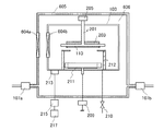
図1は本実施の形態の成膜装置の断面概略図である。 FIG. 1 is a schematic sectional view of a film forming apparatus according to the present embodiment.
図1に示す成膜装置は、隔壁605の内部に成膜室103を備え、隔壁605と成膜室103との間に空間606を有する。
The film formation apparatus illustrated in FIG. 1 includes a
はじめに、成膜室103を囲う隔壁605の構成について説明する。
First, the structure of the
隔壁605は空間606にガスを供給するためのガス導入手段107a、圧力調整手段107b、並びに搬入出口604aを備える。
The
隔壁605は成膜室103と大気との間に空間606を形成するために設けられる。隔壁605は大気に含まれる不純物を透過しなければ良く、例えば鉄、アルミニウム、ステンレス等の金属で構成されても良いし、または大気に含まれる不純物を透過しない十分な厚さや、透過防止膜(バリア膜)を持つ、可撓性を有する袋体を用いることができる。なお、大気に含まれる不純物としては、酸化物半導体層を成膜する場合は例えば水など、水素原子を含む化合物をその例に挙げることができる。
A
搬入出口604aは、被処理基板を隔壁605内に搬入及び搬出するための搬入出口である。搬入出口604aは開閉可能な扉を有し、基板を搬入出するときに扉を開いて隔壁605に開口部を形成する。搬入出口604aを開口することで、空間606の圧力が大気圧まで低下し、大気に含まれる不純物が空間606の封止ガスに拡散する恐れがある。従って、搬入出口604aの開口後は空間606の封止ガスを高純度なガスで充分置換し、例えば、水素原子を含む化合物の濃度を1ppm以下、好ましくは0.1ppm以下とすることが好ましい。
The loading / unloading
圧力調整手段107bは、例えば圧力センサとバルブ及び排気ラインで構成されていて良く、内部の圧力が設定値よりも高い場合はバルブを開け、また内部の圧力が設定値よりも低い場合はバルブを閉じることにより圧力を調整できる。 The pressure adjusting means 107b may be composed of, for example, a pressure sensor, a valve, and an exhaust line. When the internal pressure is higher than the set value, the valve is opened, and when the internal pressure is lower than the set value, the valve is opened. The pressure can be adjusted by closing.
ガス導入手段107aと圧力調整手段107bを用いて、空間606にアルゴンなどの希ガスからなる封止ガスを導入できる。この封止ガスには水素原子を含む化合物が含まれないことが望ましく、水素原子を含む化合物の濃度は1ppm以下、好ましくは0.1ppm以下とすることが好ましい。
A sealing gas made of a rare gas such as argon can be introduced into the
この封止ガスの一部は、成膜室103内の接続部や配管の継ぎ目などを介して、成膜室103の内部に漏洩(リーク)するが、リークする封止ガスの主たる成分はアルゴンなどの希ガスとなる。
A part of this sealing gas leaks into the
また、隔壁605の接続部や配管の継ぎ目などを介して、大気中から空間606へ酸素や窒素、H2O等の水素原子を含む化合物が不純物として漏洩(リーク)するが、ガス導入手段107aと圧力調整手段107bを用いて、空間606の圧力を大気圧より大きくすることにより、その影響を抑制することができる。
Further, a compound containing hydrogen atoms such as oxygen, nitrogen, H 2 O and the like leaks from the atmosphere into the
次に、成膜室103について説明する。成膜室103は、被処理基板である基板110を保持するための基板保持部201、基板加熱手段203、基板回転手段205、ターゲット保持部に保持されたスパッタリング用ターゲット211、防着板212、メインバルブ213、及び搬入出口604b、を有する。なお、スパッタリング用ターゲット211と基板110の間にはシャッター(図示しない)が設けられている。また、電源209、ガス導入手段210、自動圧力制御装置215、及び排気手段217は、隔壁605の外部に配置され、配管等を用いて直接成膜室103へ接続されている。
Next, the
排気手段217としては、例えばクライオポンプなどの排気手段を用いることが好ましい。酸化物半導体層を成膜する場合、膜中に混入する不純物の量を低く抑えることができるためである。
As the
ガス導入手段210は、例えばマスフローコントローラ等で制御された電磁バルブ等を介してガス供給ラインに接続すればよい。マスフローコントローラを用いることにより、複数のガスの混合比が制御されたガスを成膜室103に導入できる。なお、成膜室103内に不純物が混入するのを防ぐため、成膜室103に導入するガスとしては高純度のガスを用いる。例えば、成膜室103内に導入されるこれらのガスは、装置内に導入される前にガス精製機により高純度化されたものを用いる。これにより、ガス中に含まれる水等の不純物を予め除去することができるため、装置内部にこれらの不純物が導入されるのを防ぐことができる。
The
基板保持部201は、基板110を保持する役割を有する。また、基板保持部201は、基板加熱手段203を備える。基板加熱手段203としては、例えば、抵抗発熱体などの発熱体からの熱伝導または熱輻射によって、被処理物を加熱する手段を用いてもよいし、ランプから発する光(電磁波)の輻射により被処理物を加熱する手段を用いてもよい。基板加熱手段203を設けることにより基板110を加熱しながら成膜を行うことができる。
The
基板回転手段205は基板110を回転できる。基板110を回転しながら成膜すると膜厚の均一性が高まるため好ましい。
The substrate rotating means 205 can rotate the
防着板212は、成膜時に基板に付着しなかった成膜材料が、成膜室103の内壁に付着し、ゴミの発生原因となるのを防ぐ。防着板212の材料としては、鉄、アルミニウム、ステンレス等の金属を用いることができる。
The
なお、成膜室103は、基板保持部201周辺の壁面を加熱する手段(図示しない)を有していてもよい。定期的に成膜室の内壁を加熱し、内壁に吸着する不純物を脱離処理することで高真空を実現することができる。
Note that the
搬入出口604bは被処理基板を成膜室103に搬入及び搬出するための搬入出口である。搬入出口604bは開閉可能な扉を有し、基板を搬入出するときに扉を開いて成膜室103に開口部を形成する。
The loading / unloading
なお、成膜室103は、基板110を成膜装置内に搬入するためのロードロック室と、ロードロック室から成膜室に基板を搬送するための搬送室とを備えていても良い。
Note that the
次に、上述の、成膜室、搬送室、及びロードロック室を備えた成膜装置について説明する。 Next, the film forming apparatus including the film forming chamber, the transfer chamber, and the load lock chamber will be described.
図7は、本実施の形態の成膜装置の側面概略図である。 FIG. 7 is a schematic side view of the film forming apparatus of the present embodiment.
図7に示す成膜装置100は、ロードロック室101、及び隔壁105を有し、隔壁105内には、ロードロック室101と連結された搬送室102と、搬送室102に連結された成膜室103が設けられ、それぞれの連結部にはそれぞれゲートバルブが設けられている。また、隔壁105と、搬送室102及び成膜室103との間には、空間106を有する。また、隔壁105は空間106にガスを導入するためのガス導入手段107aと圧力調整手段107bとを具備する。
A
ロードロック室101は、基板加熱手段を有する基板保持部109、排気手段222、及びガス導入手段(図示しない)を有する。なお、ロードロック室101は前記搬送室102に加えて、成膜装置の外部ともゲートバルブ104により隔てられている。
The
ロードロック室101は基板の搬入出を行う場所であると同時に、処理前の基板に対し予備加熱を行うことが可能である。またその内部は、排気手段222を用いて排気することができる。処理前の基板に対して、排気しながら予備加熱を行うことで基板に吸着した不純物を脱離し、排気することができる。なお、不純物としては、例えば水素、H2O等の水素原子を含む化合物や、炭素原子を含む化合物をその例に挙げることができる。予備加熱の温度は、室温以上600℃以下であれば良く、100℃以上400℃以下であることが特に好ましい。
The
搬送室102は搬送ロボット108、及び排気手段220を有し、基板110をロードロック室101と成膜室103との間で搬送を行うための受け渡し室の役割を有している。
The
搬送室102に設けられた排気手段220により、搬送室内を真空排気することが可能である。搬送室内を真空排気することにより、予備加熱によって不純物を除去した基板の搬送時における再汚染を抑制することができる。
The
隔壁105は上記隔壁605と同様の役割を果たす。また、同様に、空間106は、上記空間606と同様の役割を果たす。すなわち隔壁105は、隔壁105に設けられたガス導入手段107aと圧力調整手段107bにより、空間106内部に希ガスからなる封止ガスを導入して大気圧以上とすることができ、大気から空間106への不純物の混入を抑制する働きを有する。
The
搬送室102は成膜室103と同様に、隔壁105の内部に配置されている。従って前記成膜装置と同様、空間106にアルゴン等の希ガスからなる封止ガスを導入して大気圧以上とすることにより、搬送室102内の接続部や配管の継ぎ目などを介して、搬送室102の内部に漏洩(リーク)するガスの主たる成分はアルゴンなどの希ガスとなる。
Similarly to the
次に、成膜装置100を用いてガラス基板上に酸化物半導体膜を形成する方法について説明する。本実施の形態では、成膜室103でスパッタリング法を用いて酸化物半導体膜を成膜する場合について説明する。しかし、その膜種は酸化物半導体膜に限らず、スパッタリング用ターゲット211を変更することなどにより酸化物絶縁膜や窒化物絶縁膜なども成膜可能である。
Next, a method for forming an oxide semiconductor film over a glass substrate using the
成膜装置100を用いることにより、酸化物半導体に主成分以外の不純物が極力含まれないように酸化物半導体を高純度化し、I型(真性)の酸化物半導体、又はI型(真性)に限りなく近い酸化物半導体にできる。すなわち、不純物を添加してI型化するのでなく、不純物を極力取り込まないことにより、高純度化されたI型(真性半導体)又はそれに近づけて酸化物半導体を成膜する。
By using the
高純度化された酸化物半導体中にはキャリアが極めて少なく(ゼロに近く)することができる。具体的には、キャリア濃度を1×10¹²/cm3未満、好ましくは1×1011/cm3未満まで抑制できる。また、高純度化された酸化物半導体中の水素濃度は、1×1016atoms/cm3未満である。 In a highly purified oxide semiconductor, carriers can be extremely small (close to zero). Specifically, the carrier concentration can be suppressed to less than 1 × 10 12 / cm 3 , preferably less than 1 × 10 11 / cm 3 . The hydrogen concentration in the highly purified oxide semiconductor is less than 1 × 10 16 atoms / cm 3 .
まず、隔壁105に設けられたガス導入手段107aを用いて、空間106に水素原子を含む化合物の濃度が1ppm以下のアルゴンからなる封止ガスを導入する。同時に圧力調整手段107bを用いて、空間106の圧力が大気圧以上になるように調整する。
First, a sealing gas composed of argon having a concentration of a compound containing hydrogen atoms of 1 ppm or less is introduced into the
なお、ここでは封止ガスとしてアルゴンを用いたが、必ずしもこれに限定されず、他の希ガスも用いることができる。 Note that although argon is used as the sealing gas here, the present invention is not necessarily limited thereto, and other rare gases can also be used.
次に、搬送室102及び成膜室103内部を、それぞれに設けられた排気手段を用いて減圧する。
Next, the insides of the
また、成膜室103の内壁に吸着する不純物を脱離処理するため、成膜室103の内壁を定期的に加熱処理してもよい。
Further, in order to desorb impurities adsorbed on the inner wall of the
次に、ロードロック室101と外部とを仕切るゲートバルブ104を開け、基板110をロードロック室101に搬入する。搬入後、ロードロック室101に接続された排気手段222を用いて室内を減圧すると共に、基板加熱手段を用いて基板110の予備加熱を行い、基板110に付着した不純物を脱離、排気する。
Next, the
基板110に使用することができる基板に大きな制限はないが、バリウムホウケイ酸ガラスやアルミノホウケイ酸ガラスなどのガラス基板を用いる。
There is no particular limitation on a substrate that can be used as the
続いて、予備加熱を終えた基板110を、搬送ロボット108を用いて搬送室102を経由して成膜室103に搬入する。
Subsequently, the
まず、ロードロック室101と搬送室102を仕切るゲートバルブを開け、搬送ロボット108を用いて搬送室102に基板110を搬入し、上記ゲートバルブを閉じる。次いで搬送室102と成膜室103を仕切るゲートバルブを開け、同様に成膜室103に基板110を搬入する。
First, the gate valve that partitions the
なお、基板110を搬出後、真空排気されたロードロック室101内部に希ガスを充填して大気圧以上としておいても良い。こうすることで、大気からロードロック室への不純物を含んだ大気成分の混入を抑制することができる。
Note that after unloading the
基板110は、成膜室103内の基板保持部201に搬送される。基板保持部201にある基板ホルダ(図示しない)は、上下駆動機構によって上下に移動し、基板を固定することが可能である。なお、図7に示すように、フェイスダウン方式(基板の被成膜面が下を向いた状態で成膜する方式)を採用すると、基板110へのゴミの付着などを抑えることができるため、好ましい。
The
基板110を搬入後、搬送室102と成膜室103とを仕切るゲートバルブを閉じる。
After the
成膜室103内の排気手段217、メインバルブ213、自動圧力制御装置215及びガス導入手段210を用いて成膜室103内の圧力を制御しながら、高純度のスパッタリング用のガスを導入し、スパッタリング法を用いて基板110に酸化物半導体膜を成膜する。
While controlling the pressure in the
スパッタリングに用いる電源209は、DC(直流)であってもRF(高周波)のいずれを用いても良い。例えば、成膜室103において、絶縁膜を成膜する場合には、RF電源を用いたRFスパッタリング法を用いれば良く、金属からなる導電膜を成膜する場合には、DC電源を用いたDCスパッタリング法を用いれば良い。
The
成膜終了後、排気手段217を用いて成膜室103内を再び排気することにより、清浄な状態に保たれる。成膜後に成膜室103内が清浄な状態に保たれることで、成膜された酸化物半導体膜表面に吸着する不純物は効果的に低減される。
After the film formation is completed, the
そして、搬入時と同様に搬送ロボット108を用いて、成膜処理を終えた基板110を成膜室103から搬送室102を経由してロードロック室101内の基板保持部109に搬入する。搬送室102とロードロック室101とを仕切るゲートバルブを閉じた後、ロードロック室101に設けられた排気手段222を用いてロードロック室101の内圧を大気圧とする。その後、ロードロック室101と外部とを仕切るゲートバルブ104を開け、基板110を取り出す。
Then, using the
以上の工程でガラス基板上に酸化物半導体膜が成膜される。 Through the above steps, an oxide semiconductor film is formed over the glass substrate.
なお、ロードロック室101と搬送室102との間で基板110を搬送する際、それぞれの内部を希ガスで充填し、大気圧以上の同一の圧力とした状態で基板搬送を行っても良い。こうすることで、基板搬送時における大気からロードロック室101への、不純物を含んだ大気成分の混入を抑制することができる。
Note that when the
以上のように、本実施の形態の成膜装置は、搬送室及び成膜室と大気を隔てる隔壁によって設けられた、希ガスからなる封止ガスを導入可能な空間を有している。この空間に水素原子を含む化合物の濃度が1ppm以下の希ガスを主成分とする封止ガスを導入し、大気圧以上の圧力に調整することにより、水素原子を含む化合物が搬送室や成膜室へ混入することを防ぐことができる。 As described above, the film formation apparatus of this embodiment includes a space in which a sealing gas made of a rare gas can be introduced, which is provided by a partition wall that separates the transfer chamber and the film formation chamber from the atmosphere. By introducing a sealing gas mainly containing a rare gas having a concentration of 1 ppm or less of a hydrogen atom-containing compound into this space and adjusting the pressure to a pressure higher than atmospheric pressure, the compound containing hydrogen atoms can be transferred into a transfer chamber or a film. Mixing into the chamber can be prevented.
このような成膜装置を用いて酸化物半導体膜を成膜することで、酸化物半導体膜中及び、基板と酸化物半導体膜の界面に不純物が混入せず、水素濃度が十分に低減された高純度な酸化物半導体膜を形成することができる。例えばこのような高純度な酸化物半導体膜をトランジスタに適用することにより、オフ電流が低く、低消費電力のトランジスタを提供できる。 By forming an oxide semiconductor film using such a deposition apparatus, impurities are not mixed in the oxide semiconductor film and at the interface between the substrate and the oxide semiconductor film, and the hydrogen concentration is sufficiently reduced. A high-purity oxide semiconductor film can be formed. For example, by using such a high-purity oxide semiconductor film for a transistor, a transistor with low off-state current and low power consumption can be provided.
(実施の形態2)
本実施の形態では、本発明の一態様の連続成膜装置について図面を参照して説明する。
(Embodiment 2)
In this embodiment, a continuous film formation apparatus of one embodiment of the present invention is described with reference to drawings.
図2は、本実施の形態の連続成膜装置の上面概略図である。 FIG. 2 is a schematic top view of the continuous film forming apparatus of the present embodiment.
図2に示す連続成膜装置は、第1のロードロック室111、第2のロードロック室131、及び隔壁134を有する。さらに隔壁134内には、搬送室112、複数の成膜室(図2では、第1の成膜室113、第2の成膜室115、第3の成膜室117、第4の成膜室121、及び第5の成膜室127)、複数の加熱室(図2では、第1の加熱室119及び第2の加熱室123)、処理室125、基板待機室129、及び基板搬送手段133を有する。また、隔壁134と、搬送室112、複数の成膜室、複数の加熱室、処理室125、基板待機室129、及び基板搬送手段133との間には、空間135を有する。なお、図示しないが、本実施の形態の連続成膜装置は、装置の内壁を300℃以上に加熱する手段を有する。
The continuous film forming apparatus illustrated in FIG. 2 includes a first
第1のロードロック室111、搬送室112、複数の成膜室、複数の加熱室、処理室125、基板待機室129、及び第2のロードロック室131は、それぞれ排気手段1111〜1131を有する。これらの排気手段は、各室の使用用途に応じて適宜排気装置を選定すればよく、例えば、吸着型のポンプを備えた排気手段や、ターボポンプにコールドトラップを備えた排気手段等が挙げられる。特に、吸着型のポンプを備えることが好ましい。吸着型のポンプとしては、例えば、クライオポンプ、スパッタイオンポンプ、チタンサブリメーションポンプ等の、吸着手段を有するポンプが挙げられる。
The first
本実施の形態では、処理前の基板を収納する基板ホルダを有する場所として、第1のロードロック室111、処理済みの基板を収納する基板ホルダを有する場所として、第2のロードロック室131を設けたが、本発明の一態様の成膜装置は、これに限らず、一室で基板の搬入出を行っても良い。
In the present embodiment, the first
また図示しないが、第1のロードロック室111は基板加熱手段を有する。排気手段1111、及び基板加熱手段を併用し、排気しながら処理前の基板の予備加熱を行うことで、基板に付着した不純物を脱離、排気することができる。
Although not shown, the first
搬送室112は、基板搬送手段133を用いて基板をある一室から他の一室に搬送する受け渡し室の役割を有している。本実施の形態の連続成膜装置は、2つの基板搬送手段を有する構成としたが、基板搬送手段は1つ以上の任意の数だけ設ければ良い。
The
加熱室(第1の加熱室119及び第2の加熱室123)は、基板を加熱する手段を備えている。本実施の形態の連続成膜装置は、2つの加熱室を有する構成としたが、加熱室は1つ以上の任意の数だけ設ければ良い。
The heating chamber (the
処理室125は、酸素ラジカル処理を行うことができる場所である。酸素ラジカルは、酸素を含むプラズマ発生装置により供給されてもよいし、オゾン発生装置により供給されてもよい。供給された酸素ラジカル又は酸素を薄膜に照射することによって膜表面を改質することができる。また、処理室で行う処理は、酸素ラジカル処理に限定されない。連続成膜装置において、処理室は必要でなければ設けなくても良いし、複数設けても良い。
The
基板待機室129は、連続成膜の工程中の基板を待機させておくことができる場所である。基板待機室129は、冷却手段を有していても良い。冷却手段を有することで、基板待機室において、成膜等のために熱された基板を十分に冷却することができる。冷却は、ヘリウム、ネオン、アルゴン等を基板待機室129に導入して行っても良い。なお、冷却に用いる窒素、またはヘリウム、ネオン、アルゴン等の希ガスに、水、水素など水素原子を含む化合物が含まれないことが好ましい。または、窒素、またはヘリウム、ネオン、アルゴン等の希ガスの純度を、6N(99.9999%)以上、好ましくは7N(99.99999%)以上、(即ち不純物濃度を1ppm以下、好ましくは0.1ppm以下)とすることが好ましい。連続成膜装置において、基板待機室は必要でなければ設けなくても良い。
The
本発明の一態様の連続成膜装置は、複数の成膜室を有する。図2の連続成膜装置は、5つの成膜室(第1の成膜室113、第2の成膜室115、第3の成膜室117、第4の成膜室121、及び第5の成膜室127)を有する構成としたが、成膜室の数はこれに限定されず、連続成膜する膜の数に合わせて適宜定めればよい。
The continuous film formation apparatus of one embodiment of the present invention includes a plurality of film formation chambers. The continuous film formation apparatus in FIG. 2 includes five film formation chambers (a first
成膜室で行う成膜は、スパッタリング法、真空蒸着法、プラズマCVD法など、目的とする膜の種類に応じて、種々の成膜方法を用いることができる。例えば、第1の成膜室113ではスパッタリング法により窒化珪素膜、第2の成膜室115ではスパッタリング法により酸化珪素膜、第3の成膜室117、及び第4の成膜室121ではスパッタリング法により酸化物半導体膜、及び第5の成膜室127ではスパッタリング法により導電膜がそれぞれ成膜できる。
For the film formation performed in the film formation chamber, various film formation methods such as a sputtering method, a vacuum evaporation method, and a plasma CVD method can be used depending on the type of the target film. For example, a silicon nitride film is formed by a sputtering method in the first
次に、ロードロック室以外の各室(搬送室112、複数の成膜室、複数の加熱室、処理室125及び基板待機室129)を囲う、隔壁134の構成について説明する。
Next, the structure of the
隔壁134はロードロック室以外の各室と大気との間に空間135を形成するために設けられる。隔壁134は大気に含まれる不純物を透過しなければ良く、例えば鉄、アルミニウム、ステンレス等の金属で構成されても良いし、または大気に含まれる不純物を透過しない十分な厚さや、透過防止膜(バリア膜)を持つ、可撓性を有する袋体を用いることができる。なお、大気に含まれる不純物としては、酸化物半導体膜を成膜する場合は例えば水など、水素原子を含む化合物をその例に挙げることができる。
The
図示しないが、隔壁134はガス導入手段と圧力調整手段を有する。
Although not shown, the
圧力調整手段は、例えば圧力センサとバルブ及び排気ラインで構成されていて良く、内部の圧力が設定値よりも高い場合はバルブを開け、また内部の圧力が設定値よりも低い場合はバルブを閉じることにより圧力を調整できる。 The pressure adjusting means may be composed of, for example, a pressure sensor, a valve, and an exhaust line. The valve is opened when the internal pressure is higher than the set value, and is closed when the internal pressure is lower than the set value. Thus, the pressure can be adjusted.
ガス導入手段と圧力調整手段を用いて、空間135にアルゴンなどの希ガスからなる封止ガスを導入できる。この封止ガスには水素原子を含む化合物が含まれないことが望ましく、水素原子を含む化合物の濃度は1ppm以下、好ましくは0.1ppm以下とすることが好ましい。
A sealing gas made of a rare gas such as argon can be introduced into the
この封止ガスの一部は、ロードロック室以外の各室内の接続部や配管の継ぎ目などを介して、ロードロック室以外の各室の内部に漏洩(リーク)するが、リークする封止ガスの主たる成分はアルゴンなどの希ガスとなる。 A part of this sealing gas leaks into the interior of each chamber other than the loadlock chamber via the connecting part of each chamber other than the loadlock chamber and the joint of the piping. The main component is a rare gas such as argon.
また、隔壁134の接続部や隔壁134に設けられた配管の継ぎ目などを介して、大気中から空間135へ酸素や窒素、H2O等の水素原子を含む化合物が不純物として漏洩(リーク)するが、ガス導入手段と圧力調整手段を用いて、空間135の圧力を大気圧より大きくすることにより、その影響を抑制することができる。
In addition, a compound containing hydrogen atoms such as oxygen, nitrogen, and H 2 O leaks from the atmosphere to the
なお、図8に示すように、酸化物半導体膜を成膜する第3の成膜室117を隔壁134aで囲い、同様に第4の成膜室121を隔壁134bで囲う構成としてもよい。このような構成とすることで、成膜装置の大きさを図2の構成よりも小さくすることが可能となる。
Note that as illustrated in FIG. 8, the
以上のように、本実施の形態の成膜装置は、搬送室、成膜室、加熱室、処理室及び基板待機室と大気を隔てるようにして隔壁によって設けられた、希ガスからなる封止ガスを導入可能な空間を有している。この空間に水素原子を含む化合物の濃度が1ppm以下のガス、例えば希ガスを主成分とする封止ガスを導入し、大気圧以上の圧力に調整することにより、水素原子を含んだ化合物が搬送室、成膜室、加熱室、処理室及び基板待機室へ混入することを防ぐことができる。 As described above, the film formation apparatus of this embodiment mode includes a seal made of a rare gas provided by a partition so as to separate the atmosphere from a transfer chamber, a film formation chamber, a heating chamber, a processing chamber, and a substrate standby chamber. It has a space where gas can be introduced. By introducing a gas whose concentration of a compound containing hydrogen atoms is 1 ppm or less, for example, a sealing gas containing a rare gas as a main component into this space, and adjusting the pressure to a pressure higher than atmospheric pressure, the compound containing hydrogen atoms is transported. Mixing into the chamber, the film formation chamber, the heating chamber, the processing chamber, and the substrate standby chamber can be prevented.
このような連続成膜装置を用いて大気開放せずに酸化物半導体膜と、酸化物半導体膜に接する膜を連続して成膜処理を行うことで、酸化物半導体膜中、酸化物半導体に接する膜中、及びこれらの界面に水素原子を含む化合物が混入せず、水素原子濃度が十分に低減された高純度な酸化物半導体膜を積層することができる。また、当該積層膜を用いて半導体装置を作製することができる。例えばこのような高純度な酸化物半導体膜をトランジスタに適用することにより、オフ電流が低く、低消費電力のトランジスタを提供できる。 Using such a continuous film formation apparatus, the oxide semiconductor film and the film in contact with the oxide semiconductor film are continuously formed without being exposed to the atmosphere. A high-purity oxide semiconductor film in which a hydrogen atom concentration is sufficiently reduced without being mixed with a compound containing a hydrogen atom in a film in contact with each other and an interface between these films can be stacked. In addition, a semiconductor device can be manufactured using the stacked film. For example, by using such a high-purity oxide semiconductor film for a transistor, a transistor with low off-state current and low power consumption can be provided.
(実施の形態3)
本実施の形態では、実施の形態2に示した連続成膜装置を用いてボトムゲート型のトランジスタを作製する方法について図2乃至図4を用いて説明する。本実施の形態では、半導体層に酸化物半導体を用いたトランジスタを作製する方法について説明する。
(Embodiment 3)
In this embodiment, a method for manufacturing a bottom-gate transistor with the use of the continuous deposition apparatus described in Embodiment 2 will be described with reference to FIGS. In this embodiment, a method for manufacturing a transistor including an oxide semiconductor in a semiconductor layer will be described.
本実施の形態で例示する半導体装置は、高純度化された酸化物半導体層を有する。実施の形態1又は2で例示する成膜装置を用いることにより、酸化物半導体に主成分以外の不純物が極力含まれないように酸化物半導体を高純度化し、I型(真性)の酸化物半導体、又はI型(真性)に限りなく近い酸化物半導体にできる。すなわち、不純物を添加してI型化するのでなく、不純物を極力取り込まないことにより、高純度化されたI型(真性半導体)又はそれに近づけて酸化物半導体を成膜する。従って、本実施の形態で作製するトランジスタは、高純度化及び電気的にI型(真性)化された酸化物半導体層を有する。
The semiconductor device illustrated in this embodiment includes a highly purified oxide semiconductor layer. By using the film formation apparatus exemplified in
高純度化された酸化物半導体中にはキャリアが極めて少なく(ゼロに近く)することができる。具体的には、キャリア濃度を1×10¹²/cm3未満、好ましくは1×1011/cm3未満まで抑制できる。また、高純度化された酸化物半導体中の水素濃度は、1×1016atoms/cm3未満である。 In a highly purified oxide semiconductor, carriers can be extremely small (close to zero). Specifically, the carrier concentration can be suppressed to less than 1 × 10 12 / cm 3 , preferably less than 1 × 10 11 / cm 3 . The hydrogen concentration in the highly purified oxide semiconductor is less than 1 × 10 16 atoms / cm 3 .
実施の形態1又は2に例示する成膜装置を用いることで、酸化物半導体に含まれるキャリアを極めて少なく抑制できる。このような高純度化された酸化物半導体層をトランジスタのチャネル形成領域に適用することにより、オフ状態における電流値、所謂オフ電流を少なくすることができる。なお、オフ電流は少なければ少ないほど消費電力を低減できるため好ましい。
With the use of the film formation apparatus exemplified in
本実施の形態で例示するボトムゲート型のトランジスタ300の断面図を図3(A)に示す。トランジスタ300は、ゲート電極層303、第1のゲート絶縁層305、第2のゲート絶縁層307、高純度化された酸化物半導体層312、ソース電極層311a、ドレイン電極層311b、絶縁層313、及び保護絶縁層315を有する。
A cross-sectional view of a
トランジスタ300を実施の形態2で例示する連続成膜装置を用いて作製する方法について、図4を用いて説明する。
A method for manufacturing the
まず、基板301上に導電膜を形成し、第1のフォトマスクを用いてレジストマスクを形成し、エッチングによりゲート電極層303を形成する(図4(A))。
First, a conductive film is formed over the
基板301に使用することができる基板に大きな制限はないが、バリウムホウケイ酸ガラスやアルミノホウケイ酸ガラスなどのガラス基板を用いる。
There is no particular limitation on a substrate that can be used as the
なお、下地となる絶縁層を基板301とゲート電極層303との間に設けてもよい。当該絶縁層には、基板301からの不純物元素(例えばLi、Naなどのアルカリ金属、及びCaなどのアルカリ土類金属など)の拡散を防止する機能があり、窒化シリコン膜、酸化シリコン膜、窒化酸化シリコン膜、酸化窒化シリコン膜などから選ればれた一または複数の膜による積層構造により形成することができる。
Note that an insulating layer serving as a base may be provided between the
ゲート電極層303を形成する導電膜の材料としては、モリブデン、チタン、クロム、タンタル、タングステン、アルミニウム、銅、ネオジム、スカンジウム等の金属材料またはこれらを主成分とする合金材料若しくは導電性酸化物を用いて、単層でまたは積層して形成することができる。
As a material for the conductive film for forming the
また、ゲート電極層に銅を用いる場合は、下地となる層にCu−Mg−Al合金を設け、その上に銅を形成する構成が好ましい。Cu−Mg−Al合金を設けることで、酸化膜などの下地と銅の密着性が高まる効果を奏する。 In the case where copper is used for the gate electrode layer, a structure in which a Cu—Mg—Al alloy is provided as a base layer and copper is formed thereover is preferable. By providing the Cu—Mg—Al alloy, there is an effect that the adhesion between the base such as an oxide film and copper is increased.
また、ゲート電極層に、インジウム錫酸化物、酸化タングステンを含むインジウム酸化物、酸化タングステンを含むインジウム亜鉛酸化物、酸化チタンを含むインジウム酸化物、酸化チタンを含むインジウム錫酸化物、インジウム亜鉛酸化物、酸化ケイ素を添加したインジウム錫酸化物などの透光性を有する導電性材料を、適用することもできる。また、上記透光性を有する導電性材料と、上記金属元素の積層構造とすることもできる。 In addition, in the gate electrode layer, indium tin oxide, indium oxide containing tungsten oxide, indium zinc oxide containing tungsten oxide, indium oxide containing titanium oxide, indium tin oxide containing titanium oxide, indium zinc oxide Alternatively, a light-transmitting conductive material such as indium tin oxide to which silicon oxide is added can be used. Alternatively, a stacked structure of the above light-transmitting conductive material and the above metal element can be employed.
また、ゲート電極層とゲート絶縁層の間に、ゲート絶縁層に接する材料層を設けても良い。当該ゲート絶縁層に接する材料層としては、窒素を含むIn−Ga−Zn−O膜や、窒素を含むIn−Sn−O膜や、窒素を含むIn−Ga−O膜や、窒素を含むIn−Zn−O膜や、窒素を含むSn−O膜や、窒素を含むIn−O膜や、金属窒化膜(InN、ZnNなど)を用いることができる。これらの膜は5eV、好ましくは5.5eV以上の仕事関数を有し、トランジスタの電気特性のしきい値電圧をプラスにすることができ、所謂ノーマリーオフのスイッチング素子を実現できる。 Further, a material layer in contact with the gate insulating layer may be provided between the gate electrode layer and the gate insulating layer. As the material layer in contact with the gate insulating layer, an In—Ga—Zn—O film containing nitrogen, an In—Sn—O film containing nitrogen, an In—Ga—O film containing nitrogen, or an In containing nitrogen A —Zn—O film, a Sn—O film containing nitrogen, an In—O film containing nitrogen, or a metal nitride film (InN, ZnN, or the like) can be used. These films have a work function of 5 eV, preferably 5.5 eV or more, can increase the threshold voltage of the electrical characteristics of the transistor, and can realize a so-called normally-off switching element.
例えば、窒素を含むIn−Ga−Zn−O膜を用いる場合、少なくとも酸化物半導体層より高い窒素濃度、具体的には7原子%以上のIn−Ga−Zn−O膜を用いる。 For example, when an In—Ga—Zn—O film containing nitrogen is used, an In—Ga—Zn—O film with a nitrogen concentration higher than that of at least the oxide semiconductor layer, specifically, 7 atomic% or more is used.
次に、実施の形態2に示した連続成膜装置(図2参照)を用いて、ゲート絶縁層、酸化物半導体膜、及び導電膜を大気にさらすことなく連続成膜する。 Next, using the continuous film formation apparatus described in Embodiment 2 (see FIG. 2), the gate insulating layer, the oxide semiconductor film, and the conductive film are successively formed without being exposed to the air.
まず、隔壁134に設けられたガス導入手段を用いて、空間135に水素原子を含む化合物の濃度が1ppm以下のアルゴンからなる封止ガスを導入する。同時に圧力調整手段を用いて、空間135の圧力が大気圧以上になるように調整する。空間135の圧力を大気圧以上に調整することで、水素原子を含む化合物の、空間135への混入を抑制することができる。
First, a sealing gas composed of argon having a concentration of a compound containing hydrogen atoms of 1 ppm or less is introduced into the
なお、ここでは封止ガスとしてアルゴンを用いたが、必ずしもこれに限定されず、他の希ガスも用いることができる。 Note that although argon is used as the sealing gas here, the present invention is not necessarily limited thereto, and other rare gases can also be used.
次に、あらかじめゲート電極層303が形成された基板301を連続成膜装置の第1のロードロック室111に搬入する。そして、排気手段1111を用いて第1のロードロック室111内を減圧する。さらに基板加熱手段を用いて基板301の予備加熱を行い、基板301に付着した不純物(例えば水素原子やH2Oなどの水素原子を含む化合物など)を脱離、排気する。
Next, the
連続成膜装置において、基板301は、搬送室112を経由して、ある部屋から別の部屋まで搬送される。搬送室112内の圧力は、クライオポンプなどの排気手段1112を用いて、真空排気されている。なお、空間135をアルゴンで満たすことにより、搬送室112の内部に装置の接続部や配管の継ぎ目を介して漏洩(リーク)するガス中の不純物濃度が極めて低減されている。そのため、搬送室112内部は不純物が低減された、極めて清浄な状態にある。また、定期的に装置の内壁を加熱し、内壁に吸着する不純物を脱離処理することで高真空を実現できる。
In the continuous film formation apparatus, the
基板301を、基板搬送手段133を用いて、第1の成膜室113に搬送する。次いで、クライオポンプなどの排気手段1113を用いて第1の成膜室113の内圧を制御しながら高純度のスパッタリング用のガスを導入し、スパッタリング法を用いて、基板301及びゲート電極層303上に第1のゲート絶縁層305となる窒化珪素膜を成膜する。成膜終了後に第1の成膜室113内は、排気手段1113を用いて再び排気され、第1の成膜室113内が清浄な状態に保たれる。成膜後に第1の成膜室113内が清浄に保たれることで、第1のゲート絶縁層305の膜中及び界面に含まれる不純物は効果的に低減される。
The
そして、基板301を第1の成膜室113から第2の成膜室115に搬送し、スパッタリング法を用いて第1のゲート絶縁層305上に酸化珪素膜を成膜して、第2のゲート絶縁層307を形成する。成膜前後において、第2の成膜室115内は、排気手段1115を用いて排気され清浄な状態に保たれる。
Then, the
本実施の形態で作製する半導体装置に用いるI型化又は実質的にI型化された酸化物半導体は、界面準位及び界面電荷に対して極めて敏感であるため、酸化物半導体層とゲート絶縁層との界面は半導体装置の特性を制御する上で重要である。そのため高純度化された酸化物半導体に接する第2のゲート絶縁層307は、不純物や固定電荷を含まず、高品質な絶縁層であることが要求される。ここで、空間135をアルゴンで満たすことにより、第1の成膜室113及び第2の成膜室115の内部に、装置の接続部や配管の継ぎ目を介して漏洩(リーク)するガス中の不純物濃度が極めて低減されている。そのため、第1の成膜室113及び第2の成膜室115内部は不純物が低減された、極めて清浄な状態にある。このような成膜室内で積層された窒化珪素膜と酸化珪素膜は、不純物濃度が抑制されたゲート絶縁層として機能する。
An I-type or substantially I-type oxide semiconductor used for the semiconductor device manufactured in this embodiment is extremely sensitive to an interface state and an interface charge; The interface with the layer is important in controlling the characteristics of the semiconductor device. Therefore, the second
本実施の形態では、ゲート絶縁層を、窒化珪素膜と酸化珪素膜の積層構造としたが、ゲート絶縁層はこれに限らず、窒化珪素膜、酸化珪素膜、酸化窒化珪素膜、窒化酸化珪素膜、酸化アルミニウム膜等の単層又は積層構造とすることができる。後に形成する酸化物半導体層と接する層は酸化物絶縁膜を用いることが好ましい。ゲート絶縁層の形成方法としてはプラズマCVD法又はスパッタリング法等を用いることができるが、層中に水素が多量に含まれないようにするためには、スパッタリング法で成膜することが好ましい。ゲート絶縁層の厚さは特に限定されないが、例えば、10nm以上500nm以下とすることができる。 In this embodiment, the gate insulating layer has a stacked structure of a silicon nitride film and a silicon oxide film; however, the gate insulating layer is not limited to this, and a silicon nitride film, a silicon oxide film, a silicon oxynitride film, and a silicon nitride oxide film A single layer or a laminated structure such as a film or an aluminum oxide film can be used. An oxide insulating film is preferably used for a layer in contact with the oxide semiconductor layer to be formed later. As a method for forming the gate insulating layer, a plasma CVD method, a sputtering method, or the like can be used. However, in order to prevent a large amount of hydrogen from being contained in the layer, it is preferable to form the film by a sputtering method. Although the thickness of a gate insulating layer is not specifically limited, For example, it is 10 nm or more and 500 nm or less.
次に、基板301を、第2の成膜室115から第3の成膜室117に搬送し、第2のゲート絶縁層307上に、スパッタリング法を用いて、酸化物半導体膜309を成膜する。処理前後において、第3の成膜室117は排気手段1117を用いて真空排気されている。また、空間135をアルゴンで満たすことにより、装置の接続部や配管の継ぎ目を介して第3の成膜室117内部に漏洩(リーク)するガス中の不純物濃度が極めて低減されている。そのため、第3の成膜室117内部は不純物が低減された、極めて清浄な状態にある。成膜前後に清浄に保たれた成膜室で酸化物半導体膜309を成膜するため、酸化物半導体膜309に含まれる不純物は効果的に低減される。
Next, the
酸化物半導体膜309に用いる酸化物半導体は、四元系金属酸化物であるIn−Sn−Ga−Zn−O系酸化物半導体や、三元系金属酸化物であるIn−Ga−Zn−O系酸化物半導体、In−Sn−Zn−O系酸化物半導体、In−Al−Zn−O系酸化物半導体、Sn−Ga−Zn−O系酸化物半導体、Al−Ga−Zn−O系酸化物半導体、Sn−Al−Zn−O系酸化物半導体や、二元系金属酸化物であるIn−Zn−O系酸化物半導体、Sn−Zn−O系酸化物半導体、Al−Zn−O系酸化物半導体、Zn−Mg−O系酸化物半導体、Sn−Mg−O系酸化物半導体、In−Mg−O系酸化物半導体、In−Ga−O系酸化物半導体や、In−O系酸化物半導体、Sn−O系酸化物半導体、Zn−O系酸化物半導体などを用いることができる。また、上記酸化物半導体にInとGaとSnとZn以外の元素、例えばSiO2を含んでもよい。ここで、例えば、In−Ga−Zn−O系酸化物半導体とは、少なくともInとGaとZnを含む酸化物であり、その組成比に特に制限はない。また、InとGaとZn以外の元素を含んでもよい。
An oxide semiconductor used for the
酸化物半導体膜は、非単結晶であり、且つ酸化物半導体膜全体が非晶質状態(アモルファス状態)ではない。酸化物半導体膜全体が非晶質状態(アモルファス状態)ではないため、電気特性が不安定な非晶質の形成が抑制される。 The oxide semiconductor film is non-single crystal and the entire oxide semiconductor film is not in an amorphous state (amorphous state). Since the entire oxide semiconductor film is not in an amorphous state (amorphous state), formation of amorphous with unstable electrical characteristics is suppressed.
また、酸化物半導体膜309は、化学式InMO3(ZnO)m(m>0、且つmは自然数ではない)で表記される薄膜を用いることができる。ここで、Mは、Ga、Al、MnおよびCoから選ばれた一または複数の金属元素を示す。例えばMとして、Ga、Ga及びAl、Ga及びMn、またはGa及びCoなどがある。
The
また、酸化物半導体としてIn−Zn−O系の材料を用いる場合、用いるターゲットの組成比は、原子数比で、In:Zn=50:1〜1:2(モル数比に換算するとIn2O3:ZnO=25:1〜1:4)、好ましくはIn:Zn=20:1〜1:1(モル数比に換算するとIn2O3:ZnO=10:1〜2:1)、さらに好ましくはIn:Zn=15:1〜1.5:1(モル数比に換算するとIn2O3:ZnO=15:2〜3:4)とする。例えば、In−Zn−O系酸化物半導体の形成に用いるターゲットは、原子数比がIn:Zn:O=X:Y:Zのとき、Z>1.5X+Yとする。 In the case where an In—Zn—O-based material is used as the oxide semiconductor, the composition ratio of the target used is an atomic ratio, and In: Zn = 50: 1 to 1: 2 (in terms of the molar ratio, In 2 O 3 : ZnO = 25: 1 to 1: 4), preferably In: Zn = 20: 1 to 1: 1 (In 2 O 3 : ZnO = 10: 1 to 2: 1 in terms of molar ratio), More preferably, In: Zn = 15: 1 to 1.5: 1 (In 2 O 3 : ZnO = 15: 2 to 3: 4 in terms of molar ratio). For example, a target used for forming an In—Zn—O-based oxide semiconductor satisfies Z> 1.5X + Y when the atomic ratio is In: Zn: O = X: Y: Z.
本実施の形態では、In−Ga−Zn−O系酸化物ターゲットを用いてスパッタリング法により酸化物半導体膜309を成膜する。この段階での断面図が図4(B)に相当する。酸化物半導体膜309は、希ガス(代表的にはアルゴン)雰囲気下、酸素雰囲気下、又は希ガスと酸素の混合雰囲気下において形成することができる。
In this embodiment, the
酸化物半導体膜309をスパッタリング法で作製するためのターゲットとしては、例えば、組成比として、In2O3:Ga2O3:ZnO=1:1:1[mol数比](すなわち、In:Ga:Zn=1:1:0.5[atom比])を用いることができる。また、他にも、In:Ga:Zn=1:1:1[atom比]、又はIn:Ga:Zn=1:1:2[atom比]の組成比を有するターゲットを用いてもよい。酸化物ターゲットの充填率は90.0%以上100%以下、好ましくは95.0%以上99.9%である。充填率の高い金属酸化物ターゲットを用いることにより、成膜した酸化物半導体膜は緻密な膜となる。また、ターゲットの純度は99.99%以上が好ましく、特にNa、Li等のアルカリ金属及びCaなどのアルカリ土類金属などの不純物は低減されているものが好ましい。
As a target for forming the
酸化物半導体膜309を成膜する際に用いるスパッタリング用のガスは水素、水、水酸基又は水素化物などの不純物が除去された高純度ガスを用いる。
As a sputtering gas used for forming the
成膜条件の一例としては、基板とターゲットの間との距離を100mm、圧力0.6Pa、直流(DC)電源0.5kW、酸素(酸素流量比率100%)雰囲気下の条件が適用される。なお、パルス直流電源を用いると、成膜時に発生する粉状物質(パーティクル、ごみともいう)が軽減でき、膜厚分布も均一となるために好ましい。減圧状態に保持された成膜室内に基板を保持し、基板温度を100℃以上600℃以下、好ましくは150℃以上450℃以下、より好ましくは200℃以上400℃以下とする。特に、250℃以上320℃以下の範囲が脱水化に好適である。基板を加熱しながら成膜することにより、成膜した酸化物半導体膜に含まれる不純物濃度を低減することができる。また、スパッタリングによる損傷が軽減される。 As an example of the film forming conditions, the distance between the substrate and the target is 100 mm, the pressure is 0.6 Pa, the direct current (DC) power source is 0.5 kW, and the oxygen (oxygen flow rate is 100%) atmosphere is applied. Note that a pulse direct current power source is preferable because powder substances (also referred to as particles or dust) generated in film formation can be reduced and the film thickness can be made uniform. The substrate is held in a deposition chamber kept under reduced pressure, and the substrate temperature is set to 100 ° C. to 600 ° C., preferably 150 ° C. to 450 ° C., more preferably 200 ° C. to 400 ° C. In particular, the range from 250 ° C. to 320 ° C. is suitable for dehydration. By forming the film while heating the substrate, the concentration of impurities contained in the formed oxide semiconductor film can be reduced. Further, damage due to sputtering is reduced.
なお、酸化物半導体膜中に含まれる、Li、Naなどのアルカリ金属、及びCaなどのアルカリ土類金属などの不純物は低減されていることが好ましい。具体的には、SIMSにより検出されるLiが5×1015cm−3以下、好ましくは1×1015cm−3以下、Naが5×1015cm−3以下、好ましくは1×1015cm−3以下、Kは5×1015cm−3以下、好ましくは1×1015cm−3以下であることが好ましい。 Note that impurities such as an alkali metal such as Li and Na and an alkaline earth metal such as Ca contained in the oxide semiconductor film are preferably reduced. Specifically, Li detected by SIMS is 5 × 10 15 cm −3 or less, preferably 1 × 10 15 cm −3 or less, and Na is 5 × 10 15 cm −3 or less, preferably 1 × 10 15 cm. −3 or less and K is 5 × 10 15 cm −3 or less, preferably 1 × 10 15 cm −3 or less.
アルカリ金属、及びアルカリ土類金属は酸化物半導体にとっては悪性の不純物であり、少ないほうがよい。特にアルカリ金属のうち、Naは酸化物半導体に接する絶縁膜が酸化物であった場合、その中に拡散し、Na+となる。また、酸化物半導体内において、金属と酸素の結合を分断し、あるいは結合中に割り込む。その結果、トランジスタ特性の劣化(例えば、ノーマリーオン化(しきい値の負へのシフト)、移動度の低下等)をもたらす。加えて、特性のばらつきの原因ともなる。このような問題は、特に酸化物半導体中の水素の濃度が十分に低い場合において顕著となる。したがって、酸化物半導体中の水素の濃度が5×1019cm−3以下、特に5×1018cm−3以下である場合には、アルカリ金属の濃度を上記の値にすることが強く求められる。 Alkali metals and alkaline earth metals are malignant impurities for oxide semiconductors, and it is better that they are less. In particular, among the alkali metals, Na diffuses into an Na + when the insulating film in contact with the oxide semiconductor is an oxide. Further, in the oxide semiconductor, the bond between the metal and oxygen is broken or interrupted. As a result, transistor characteristics are deteriorated (for example, normally-on (threshold shift to negative), mobility decrease, etc.). In addition, it causes variation in characteristics. Such a problem becomes prominent particularly when the concentration of hydrogen in the oxide semiconductor is sufficiently low. Therefore, when the concentration of hydrogen in the oxide semiconductor is 5 × 10 19 cm −3 or less, particularly 5 × 10 18 cm −3 or less, it is strongly required to set the alkali metal concentration to the above value. .
酸化物半導体膜309を成膜した後、酸化物半導体膜309に、酸化ラジカル処理を行うことが好ましい。本実施の形態では、処理室125で酸素ラジカル処理を行う。処理前後において、処理室125は排気手段1125を用いて真空排気されている。また、空間135をアルゴンで満たすことにより、処理室125内部に装置の接続部や配管の継ぎ目を介して漏洩(リーク)するガス中の不純物濃度が極めて低減されている。そのため、処理室125内部は不純物が低減された、極めて清浄な状態にある。
After the
酸素ラジカルは、酸素を含むプラズマ発生装置により供給されてもよいし、オゾン発生装置により供給されてもよい。供給された酸素ラジカル又は酸素を薄膜に照射することによって膜表面を改質することができる。酸素ラジカル処理の代わりに、アルゴンと酸素のラジカル処理を行ってもよい。アルゴンと酸素のラジカル処理とは、アルゴンガスと酸素ガスを導入してプラズマを発生させて薄膜表面の改質を行うことである。 The oxygen radicals may be supplied by a plasma generator containing oxygen or may be supplied by an ozone generator. The film surface can be modified by irradiating the thin film with supplied oxygen radicals or oxygen. Instead of oxygen radical treatment, radical treatment of argon and oxygen may be performed. The radical treatment of argon and oxygen is to reform the thin film surface by introducing argon gas and oxygen gas to generate plasma.
アルゴンと酸素のラジカル処理の一例について説明する。電界が印加され放電プラズマが発生している反応空間中のアルゴン原子(Ar)は、放電プラズマ中の電子により励起又は電離され、アルゴンラジカル(Ar*)やアルゴンイオン(Ar+)や電子となる。アルゴンラジカル(Ar*)はエネルギーの高い準安定状態にあり、周辺にある同種又は異種の原子と反応し、それらの原子を励起又は電離させて安定状態に戻ろうとして雪崩現象的に反応が発生する。その時に周辺に酸素があると、酸素原子(O)が励起又は電離され、酸素ラジカル(O*)や酸素イオン(O+)となる。その酸素ラジカル(O*)が被処理物である薄膜表面の材料と反応し、表面改質が行われる。なお、不活性ガスのラジカルは、反応性ガスのラジカルと比較して準安定状態が長く維持されるという特徴があり、そのためプラズマを発生させるのに不活性ガスを用いるのが一般的である。 An example of the radical treatment of argon and oxygen will be described. Argon atoms (Ar) in a reaction space where an electric field is applied and discharge plasma is generated are excited or ionized by electrons in the discharge plasma to become argon radicals (Ar * ), argon ions (Ar + ), and electrons. . Argon radical (Ar * ) is in a metastable state with high energy, reacts with the same or different atoms in the vicinity, and reacts in an avalanche phenomenon to excite or ionize those atoms to return to a stable state. To do. If oxygen is present in the vicinity at that time, oxygen atoms (O) are excited or ionized to become oxygen radicals (O * ) or oxygen ions (O + ). The oxygen radical (O * ) reacts with the material on the surface of the thin film that is the object to be processed, and surface modification is performed. Inert gas radicals are characterized in that the metastable state is maintained longer than reactive gas radicals. Therefore, it is common to use an inert gas to generate plasma.
次に、基板301を、第5の成膜室127に搬送し、酸化物半導体膜309上に、スパッタリング法を用いて、導電膜310を成膜する(図4(C))。処理前後において、第5の成膜室127は排気手段1127を用いて真空排気されている。また、空間135をアルゴンで満たすことにより、第5の成膜室127内部に装置の接続部や配管の継ぎ目を介して漏洩(リーク)するガス中の不純物濃度が極めて低減されている。そのため、第5の成膜室127内部は不純物が低減された、極めて清浄な状態にある。
Next, the
導電膜の材料としては、例えば、Al、Cr、Cu、Ta、Ti、Mo、Wからから選ばれた元素、または上述した元素を成分とする合金か、上述した元素を組み合わせた合金等を用いることができる。また、Al膜、Cu膜などの金属膜の下側又は上側の一方または双方にTi膜、Mo膜、W膜などの高融点金属膜を積層させた構成としても良い。また、Al膜に生ずるヒロックやウィスカーの発生を防止する元素(Si、Nd、Scなど)が添加されているAl材料を用いることで耐熱性を向上させることが可能となる。また導電膜は、導電性の金属酸化物を用いて形成しても良い。導電性の金属酸化物としては酸化インジウム(In2O3)、酸化スズ(SnO2)、酸化亜鉛(ZnO)、酸化インジウム酸化スズ合金(In2O3−SnO2、ITOと略記する)、酸化インジウム酸化亜鉛合金(In2O3−ZnO)またはこれらの金属酸化物材料に酸化珪素を含ませたものを用いることができる。 As a material of the conductive film, for example, an element selected from Al, Cr, Cu, Ta, Ti, Mo, W, an alloy containing the above-described element as a component, or an alloy combining the above-described elements is used. be able to. Alternatively, a configuration may be adopted in which a refractory metal film such as a Ti film, a Mo film, or a W film is laminated on one or both of the lower side or the upper side of a metal film such as an Al film or Cu film. In addition, heat resistance can be improved by using an Al material to which an element (Si, Nd, Sc, or the like) that prevents generation of hillocks and whiskers generated in the Al film is used. The conductive film may be formed using a conductive metal oxide. As the conductive metal oxide, indium oxide (In 2 O 3 ), tin oxide (SnO 2 ), zinc oxide (ZnO), indium oxide tin oxide alloy (In 2 O 3 —SnO 2 , abbreviated as ITO), An indium oxide-zinc oxide alloy (In 2 O 3 —ZnO) or a metal oxide material containing silicon oxide can be used.
次に、連続成膜処理が終了した基板301を当該連続成膜装置外で処理を行うため、第2のロードロック室131に搬送する。第2のロードロック室131の内圧を大気圧まで戻した後、基板を搬出する。
Next, the
なお、連続成膜の工程中に、ある部屋から搬出された基板を、次の成膜や処理を行う部屋に搬入する前に別の場所で待機させる必要が生じた場合は、基板待機室129に基板を搬入すれば良い。基板待機室129は排気手段1129を用いて真空排気されている。また、空間135をアルゴンで満たすことにより、基板待機室129内部に装置の接続部や配管の継ぎ目を介して漏洩(リーク)するガス中の不純物濃度が極めて低減されている。そのため、基板待機室129内部は不純物が低減された、極めて清浄な状態にある。
In the case where the substrate unloaded from one room needs to be waited in another place before being loaded into the room where the next film forming or processing is performed during the continuous film forming process, the
次に、導電膜310上に第2のフォトマスクを用いてレジストマスクを形成し、エッチングにより不要な導電膜310、及び酸化物半導体膜309を除去する。次いで、第3のフォトマスクを用いて、酸化物半導体層のチャネル形成領域と重畳する導電膜をエッチングし、ソース電極層311a、及びドレイン電極層311bを形成する。なお、この段階の断面図を図4(D)に示す。
Next, a resist mask is formed over the
次いで、酸化物半導体層に第1の加熱処理を行う。この第1の加熱処理によって酸化物半導体層の脱水化または脱水素化を行うことができる。第1の加熱処理の温度は、400℃以上750℃以下、または400℃以上基板の歪み点未満とする。ここでは、加熱処理装置の一つである電気炉に基板を導入し、酸化物半導体層に対して窒素雰囲気下450℃において1時間の加熱処理を行い、酸化物半導体層312を得る。
Next, first heat treatment is performed on the oxide semiconductor layer. Through the first heat treatment, the oxide semiconductor layer can be dehydrated or dehydrogenated. The temperature of the first heat treatment is 400 ° C. or higher and 750 ° C. or lower, or 400 ° C. or higher and lower than the strain point of the substrate. Here, a substrate is introduced into an electric furnace which is one of heat treatment apparatuses, and the oxide semiconductor layer is subjected to heat treatment at 450 ° C. for 1 hour in a nitrogen atmosphere, whereby the
なお、加熱処理装置は電気炉に限られず、抵抗発熱体などの発熱体からの熱伝導または熱輻射によって、被処理物を加熱する装置を用いてもよい。例えば、GRTA(Gas Rapid Thermal Anneal)装置、LRTA(Lamp Rapid Thermal Anneal)装置等のRTA(Rapid Thermal Anneal)装置を用いることができる。LRTA装置は、ハロゲンランプ、メタルハライドランプ、キセノンアークランプ、カーボンアークランプ、高圧ナトリウムランプ、高圧水銀ランプなどのランプから発する光(電磁波)の輻射により、被処理物を加熱する装置である。GRTA装置は、高温のガスを用いて加熱処理を行う装置である。高温のガスには、アルゴンなどの希ガス、または窒素のような、加熱処理によって被処理物と反応しない不活性気体が用いられる。 Note that the heat treatment apparatus is not limited to an electric furnace, and an apparatus for heating an object to be processed by heat conduction or heat radiation from a heating element such as a resistance heating element may be used. For example, a rapid thermal annealing (RTA) device such as a GRTA (Gas Rapid Thermal Anneal) device or an LRTA (Lamp Rapid Thermal Anneal) device can be used. The LRTA apparatus is an apparatus that heats an object to be processed by radiation of light (electromagnetic waves) emitted from a lamp such as a halogen lamp, a metal halide lamp, a xenon arc lamp, a carbon arc lamp, a high pressure sodium lamp, or a high pressure mercury lamp. The GRTA apparatus is an apparatus that performs heat treatment using a high-temperature gas. As the high-temperature gas, an inert gas that does not react with an object to be processed by heat treatment, such as nitrogen or a rare gas such as argon, is used.
例えば、第1の加熱処理として、650℃〜700℃の高温に加熱した不活性ガス中に基板を移動させて入れ、数分間加熱した後、基板を移動させて高温に加熱した不活性ガス中から出すGRTAを行ってもよい。 For example, as the first heat treatment, the substrate is moved into an inert gas heated to a high temperature of 650 ° C. to 700 ° C., heated for several minutes, and then moved to a high temperature by moving the substrate to a high temperature. GRTA may be performed from
なお、第1の加熱処理においては、窒素、またはヘリウム、ネオン、アルゴン等の希ガスに、水、水素などが含まれないことが好ましい。または、加熱処理装置に導入する窒素、またはヘリウム、ネオン、アルゴン等の希ガスの純度を、6N(99.9999%)以上好ましくは7N(99.99999%)以上(即ち不純物濃度を1ppm以下、好ましくは0.1ppm以下)とすることが好ましい。 Note that in the first heat treatment, it is preferable that water, hydrogen, or the like be not contained in nitrogen or a rare gas such as helium, neon, or argon. Alternatively, the purity of nitrogen or a rare gas such as helium, neon, or argon introduced into the heat treatment apparatus is 6N (99.9999%) or more, preferably 7N (99.99999%) or more (that is, the impurity concentration is 1 ppm or less, Preferably it is 0.1 ppm or less.
また、第1の加熱処理で酸化物半導体層を加熱した後、同じ炉に高純度の酸素ガス、高純度のN2Oガス、又は超乾燥エア(露点が−40℃以下、好ましくは−60℃以下)を導入してもよい。酸素ガスまたはN2Oガスに、水、水素などが含まれないことが好ましい。または、加熱処理装置に導入する酸素ガスまたはN2Oガスの純度を、6N以上好ましくは7N以上(即ち、酸素ガスまたはN2Oガス中の不純物濃度を1ppm以下、好ましくは0.1ppm以下)とすることが好ましい。酸素ガス又はN2Oガスの作用により、脱水化または脱水素化処理による不純物の排除工程によって同時に減少してしまった酸化物半導体を構成する主成分材料である酸素を供給することによって、酸化物半導体層を高純度化及び電気的にI型(真性)化する。 In addition, after the oxide semiconductor layer is heated by the first heat treatment, high-purity oxygen gas, high-purity N 2 O gas, or ultra-dry air (with a dew point of −40 ° C. or lower, preferably −60 ° C.) in the same furnace. May be introduced). It is preferable that water, hydrogen, and the like are not contained in the oxygen gas or N 2 O gas. Alternatively, the purity of the oxygen gas or N 2 O gas introduced into the heat treatment apparatus is 6 N or more, preferably 7 N or more (that is, the impurity concentration in the oxygen gas or N 2 O gas is 1 ppm or less, preferably 0.1 ppm or less). It is preferable that By supplying oxygen, which is a main component material of the oxide semiconductor, which is simultaneously reduced by the impurity removal step by dehydration or dehydrogenation treatment by the action of oxygen gas or N 2 O gas, the oxide The semiconductor layer is highly purified and electrically made I-type (intrinsic).
その後、再び第1のロードロック室111から基板301を搬入し、予備加熱を行った後、処理室125にて、N2O、N2、またはArなどのガスを用いたプラズマ処理を行い、露出している酸化物半導体層の表面に付着した吸着水などを除去してもよい。プラズマ処理を行った場合、大気に触れることなく、酸化物半導体層の一部に接する保護絶縁層となる絶縁層313を形成できる。
After that, the
絶縁層313は、少なくとも1nm以上の膜厚とし、スパッタリング法など、絶縁層313に水、水素等の不純物を混入させない方法を適宜用いて形成することができる。絶縁層313に水素が含まれると、その水素の酸化物半導体層への侵入、又は水素による酸化物半導体層中の酸素の引き抜き、が生じ酸化物半導体層312のバックチャネルが低抵抗化(N型化)してしまい、寄生チャネルが形成されるおそれがある。よって、絶縁層313はできるだけ水素を含まない膜になるように、成膜方法に水素を用いないことが重要である。
The insulating
絶縁層313の成膜は第1の成膜室113で行う。第1の成膜室113は排気手段1113を用いて真空排気されている。また、空間135をアルゴンで満たすことにより、成膜室内部に装置の接続部や配管の継ぎ目を介して漏洩(リーク)するガス中の不純物濃度が極めて低減されている。そのため、成膜室内部は不純物が低減された、極めて清浄な状態にある。
The insulating
酸化物半導体層312に接して形成する絶縁層313は、水分や、水素イオンや、OH−などの不純物を含まず、これらが外部から侵入することを防ぐ無機絶縁膜を用いる。特に、酸化物絶縁膜を用いることが好ましい。代表的には酸化珪素膜、酸化窒化珪素膜、酸化アルミニウム膜、または酸化窒化アルミニウム膜などを用いる。
The insulating
本実施の形態では、絶縁層313として膜厚200nmの酸化珪素膜を、スパッタリング法を用いて成膜する。成膜時の基板温度は、室温以上500℃以下とすれば良い。酸化珪素膜のスパッタリング法による成膜は、希ガス(代表的にはアルゴン)雰囲気下、酸素雰囲気下、または希ガスと酸素の混合雰囲気下において行うことができる。絶縁層313を、成膜する際に用いるスパッタリング用のガスは水素、水、水酸基又は水素化物などの不純物が除去された高純度ガスを用いることが好ましい。スパッタリング用ターゲットとしては、酸化珪素ターゲットまたは珪素ターゲットを用いることができる。例えば、珪素ターゲットを用いて、酸素を含む雰囲気下でスパッタ法により酸化珪素膜を形成することができる。
In this embodiment, a 200-nm-thick silicon oxide film is formed as the insulating
次いで、第2の加熱処理を第1の加熱室119にて行う。なお、第1の加熱室119は排気手段1119を用いて真空排気されている。また、空間135をアルゴンで満たすことにより、加熱室内部に装置の接続部や配管の継ぎ目を介して漏洩(リーク)するガス中の不純物濃度が極めて低減されている。そのため、加熱室内部は不純物が低減された、極めて清浄な状態にある。第2の加熱処理は不活性ガス雰囲気下、または酸素ガス雰囲気下で、好ましくは200℃以上400℃以下、例えば250℃以上350℃以下で行う。例えば、窒素雰囲気下で250℃、1時間の第2の加熱処理を行う。第2の加熱処理を行うと、酸化物半導体層の一部(チャネル形成領域)が絶縁層313と接した状態で加熱される。
Next, second heat treatment is performed in the
以上の工程を経ることによって、酸化物半導体層に対して第1の加熱処理を行って水素、水分、水酸基又は水素化物(水素化合物ともいう)などの不純物を酸化物半導体層より意図的に排除し、かつ不純物の排除工程によって同時に減少してしまう酸化物半導体を構成する主成分材料の一つである酸素を供給することができる。よって、酸化物半導体層は高純度化及び電気的にI型(真性)化する。 Through the above steps, the first heat treatment is performed on the oxide semiconductor layer, and impurities such as hydrogen, moisture, a hydroxyl group, or hydride (also referred to as a hydrogen compound) are intentionally removed from the oxide semiconductor layer. In addition, oxygen that is one of the main component materials of the oxide semiconductor that is simultaneously reduced by the impurity removal step can be supplied. Thus, the oxide semiconductor layer is highly purified and electrically i-type (intrinsic).
絶縁層313上にさらに保護絶縁層315を形成してもよい。例えば、RFスパッタ法を用いて窒化珪素膜を形成する。RFスパッタ法は、量産性がよいため、保護絶縁層の成膜方法として好ましい。保護絶縁層は、水分などの不純物を含まず、これらが外部から侵入することをブロックする無機絶縁膜を用い、窒化珪素膜、窒化アルミニウム膜などを用いる。本実施の形態では、保護絶縁層315を、窒化珪素膜を用いて形成する。
A protective insulating
絶縁層313の成膜時と同様に、保護絶縁層315を成膜する第1の成膜室113内は排気手段1113を用いて真空排気されている。また、空間135をアルゴンで満たすことにより、成膜室内部に装置の接続部や配管の継ぎ目を介して漏洩(リーク)するガス中の不純物濃度が極めて低減されている。そのため、成膜室内部は不純物が低減された、極めて清浄な状態にある。
As in the formation of the insulating
以上の工程でトランジスタ300が形成される。なお、この段階の断面図を図4(E)に示す。
Through the above process, the
以上のように、実施の形態2で示した連続成膜装置を用いてトランジスタを作製することで、酸化物半導体層中、酸化物半導体に接する層中、及びこれらの界面に不純物が混入せず、水素原子濃度が十分に低減された高純度な酸化物半導体層を有するトランジスタを作製することができる。また、酸化物半導体層に接する層も不純物が低減されているため、酸化物半導体層は高純度に保たれる。本実施の形態で例示する方法を用いて作製する高純度な酸化物半導体層を有するトランジスタはオフ電流が低く、このトランジスタを用いることにより低消費電力の半導体装置を実現できる。 As described above, by using the continuous deposition apparatus described in Embodiment 2, a transistor is manufactured, so that impurities are not mixed in an oxide semiconductor layer, a layer in contact with an oxide semiconductor, and an interface thereof. A transistor having a high-purity oxide semiconductor layer in which the hydrogen atom concentration is sufficiently reduced can be manufactured. In addition, since the impurities in the layer in contact with the oxide semiconductor layer are reduced, the oxide semiconductor layer is kept highly purified. A transistor having a high-purity oxide semiconductor layer manufactured using the method exemplified in this embodiment has low off-state current, and a semiconductor device with low power consumption can be realized by using this transistor.
(実施の形態4)
本実施の形態では、実施の形態2に示した連続成膜装置を用いて、実施の形態3で説明したトランジスタとは異なる構成を有するトランジスタを作製する方法について図2、図3、及び図5を用いて説明する。本実施の形態では、酸化物半導体層を用いた半導体装置を作製する方法について説明する。
(Embodiment 4)
In this embodiment, a method for manufacturing a transistor having a structure different from that of the transistor described in Embodiment 3 using the continuous deposition apparatus described in Embodiment 2 will be described with reference to FIGS. Will be described. In this embodiment, a method for manufacturing a semiconductor device including an oxide semiconductor layer will be described.
本実施の形態で例示するボトムゲート型のトランジスタ400の断面図を図3(B)に示す。トランジスタ400は、ゲート電極層303、第1のゲート絶縁層305、第2のゲート絶縁層307、高純度化された酸化物半導体層308、ソース電極層314a、ドレイン電極層314b、絶縁層313、及び保護絶縁層315を有する。
A cross-sectional view of the
トランジスタ400を実施の形態2で例示する連続成膜装置を用いて作製する方法について、図5を用いて説明する。まず、実施の形態3と同様の方法で、基板301上に導電膜を形成し、第1のフォトマスクを用いてレジストマスクを形成し、エッチングによりゲート電極層303を形成する。なお、この段階の断面図を図5(A)に示す。
A method for manufacturing the
次に、実施の形態2に示した連続成膜装置(図2参照)を用いて、ゲート絶縁層(第1のゲート絶縁層305、第2のゲート絶縁層307)及び酸化物半導体膜306を大気にさらすことなく連続成膜する。ゲート絶縁層及び酸化物半導体膜306の成膜は、実施の形態3と同様の方法で行えば良い。なお、この段階の断面図を図5(B)に示す。
Next, using the continuous deposition apparatus (see FIG. 2) described in Embodiment 2, the gate insulating layer (the first
次に、連続成膜装置外において、第2のフォトマスクを用いてレジストマスクを形成し、フォトリソグラフィ工程により酸化物半導体膜306を、島状の酸化物半導体層308に加工する。酸化物半導体層308を形成するためのレジストマスクは、インクジェット法で形成してもよい。レジストマスクをインクジェット法で形成するとフォトマスクを使用しないため、製造コストを低減できる。なお、この段階の断面図を図5(C)に示す。
Next, a resist mask is formed using a second photomask outside the continuous deposition apparatus, and the
なお、ここでの酸化物半導体膜306のエッチングは、ドライエッチングでもウェットエッチングでもよく、両方を用いてもよい。例えば、酸化物半導体膜306のウェットエッチングに用いるエッチング液としては、燐酸と酢酸と硝酸を混ぜた溶液などを用いることができる。また、ITO07N(関東化学社製)を用いてもよい。
Note that the etching of the
次いで、酸化物半導体層に第1の加熱処理を行う。この第1の加熱処理によって酸化物半導体層の脱水化または脱水素化を行うことができる。第1の加熱処理の温度は、400℃以上750℃以下、または400℃以上基板の歪み点未満とする。ここでは、加熱処理装置の一つである電気炉に基板を導入し、酸化物半導体層に対して窒素雰囲気下450℃において1時間の加熱処理を行った後、大気に触れることなく、酸化物半導体層への水や水素の再混入を防ぎ、酸化物半導体層308を得る。
Next, first heat treatment is performed on the oxide semiconductor layer. Through the first heat treatment, the oxide semiconductor layer can be dehydrated or dehydrogenated. The temperature of the first heat treatment is 400 ° C. or higher and 750 ° C. or lower, or 400 ° C. or higher and lower than the strain point of the substrate. Here, a substrate is introduced into an electric furnace which is one of heat treatment apparatuses, and the oxide semiconductor layer is subjected to heat treatment at 450 ° C. for 1 hour in a nitrogen atmosphere, and then the oxide semiconductor layer is exposed to the atmosphere without being exposed to air. The
なお、加熱処理装置は電気炉に限られず、抵抗発熱体などの発熱体からの熱伝導または熱輻射によって、被処理物を加熱する装置を用いてもよい。例えば、GRTA(Gas Rapid Thermal Anneal)装置、LRTA(Lamp Rapid Thermal Anneal)装置等のRTA(Rapid Thermal Anneal)装置を用いることができる。LRTA装置は、ハロゲンランプ、メタルハライドランプ、キセノンアークランプ、カーボンアークランプ、高圧ナトリウムランプ、高圧水銀ランプなどのランプから発する光(電磁波)の輻射により、被処理物を加熱する装置である。GRTA装置は、高温のガスを用いて加熱処理を行う装置である。高温のガスには、アルゴンなどの希ガス、または窒素のような、加熱処理によって被処理物と反応しない不活性気体が用いられる。 Note that the heat treatment apparatus is not limited to an electric furnace, and an apparatus for heating an object to be processed by heat conduction or heat radiation from a heating element such as a resistance heating element may be used. For example, a rapid thermal annealing (RTA) device such as a GRTA (Gas Rapid Thermal Anneal) device or an LRTA (Lamp Rapid Thermal Anneal) device can be used. The LRTA apparatus is an apparatus that heats an object to be processed by radiation of light (electromagnetic waves) emitted from a lamp such as a halogen lamp, a metal halide lamp, a xenon arc lamp, a carbon arc lamp, a high pressure sodium lamp, or a high pressure mercury lamp. The GRTA apparatus is an apparatus that performs heat treatment using a high-temperature gas. As the high-temperature gas, an inert gas that does not react with an object to be processed by heat treatment, such as nitrogen or a rare gas such as argon, is used.
例えば、第1の加熱処理として、650℃〜700℃の高温に加熱した不活性ガス中に基板を移動させて入れ、数分間加熱した後、基板を移動させて高温に加熱した不活性ガス中から出すGRTAを行ってもよい。 For example, as the first heat treatment, the substrate is moved into an inert gas heated to a high temperature of 650 ° C. to 700 ° C., heated for several minutes, and then moved to a high temperature by moving the substrate to a high temperature. GRTA may be performed from
なお、第1の加熱処理においては、窒素、またはヘリウム、ネオン、アルゴン等の希ガスに、水、水素などが含まれないことが好ましい。または、加熱処理装置に導入する窒素、またはヘリウム、ネオン、アルゴン等の希ガスの純度を、6N(99.9999%)以上好ましくは7N(99.99999%)以上(即ち不純物濃度を1ppm以下、好ましくは0.1ppm以下)とすることが好ましい。 Note that in the first heat treatment, it is preferable that water, hydrogen, or the like be not contained in nitrogen or a rare gas such as helium, neon, or argon. Alternatively, the purity of nitrogen or a rare gas such as helium, neon, or argon introduced into the heat treatment apparatus is 6N (99.9999%) or more, preferably 7N (99.99999%) or more (that is, the impurity concentration is 1 ppm or less, Preferably it is 0.1 ppm or less.
また、第1の加熱処理で酸化物半導体層を加熱した後、同じ炉に高純度の酸素ガス、高純度のN2Oガス、又は超乾燥エア(露点が−40℃以下、好ましくは−60℃以下)を導入してもよい。酸素ガスまたはN2Oガスに、水、水素などが含まれないことが好ましい。または、加熱処理装置に導入する酸素ガスまたはN2Oガスの純度を、6N以上好ましくは7N以上(即ち、酸素ガスまたはN2Oガス中の不純物濃度を1ppm以下、好ましくは0.1ppm以下)とすることが好ましい。酸素ガス又はN2Oガスの作用により、脱水化または脱水素化処理による不純物の排除工程によって同時に減少してしまった酸化物半導体を構成する主成分材料である酸素を供給することによって、酸化物半導体層を高純度化及び電気的にI型(真性)化する。 In addition, after the oxide semiconductor layer is heated by the first heat treatment, high-purity oxygen gas, high-purity N 2 O gas, or ultra-dry air (with a dew point of −40 ° C. or lower, preferably −60 ° C.) in the same furnace. May be introduced). It is preferable that water, hydrogen, and the like are not contained in the oxygen gas or N 2 O gas. Alternatively, the purity of the oxygen gas or N 2 O gas introduced into the heat treatment apparatus is 6 N or more, preferably 7 N or more (that is, the impurity concentration in the oxygen gas or N 2 O gas is 1 ppm or less, preferably 0.1 ppm or less). It is preferable that By supplying oxygen, which is a main component material of the oxide semiconductor, which is simultaneously reduced by the impurity removal step by dehydration or dehydrogenation treatment by the action of oxygen gas or N 2 O gas, the oxide The semiconductor layer is highly purified and electrically made I-type (intrinsic).
また、酸化物半導体層の第1の加熱処理は、島状の酸化物半導体層に加工する前の酸化物半導体膜に行うこともできる。その場合には、第1の加熱処理後に、加熱処理装置から基板を取り出し、フォトリソグラフィ工程を行う。 The first heat treatment of the oxide semiconductor layer can be performed on the oxide semiconductor film before being processed into the island-shaped oxide semiconductor layer. In that case, after the first heat treatment, the substrate is taken out of the heat treatment apparatus and a photolithography process is performed.
なお、第1の加熱処理は、上記以外にも、酸化物半導体膜成膜後であれば、酸化物半導体層上にソース電極層及びドレイン電極層を積層させた後、あるいは、ソース電極層及びドレイン電極層上に絶縁層を形成した後に行っても良い。 Note that in addition to the above, the first heat treatment may be performed after the oxide semiconductor film is formed, after the source electrode layer and the drain electrode layer are stacked over the oxide semiconductor layer, or This may be performed after an insulating layer is formed on the drain electrode layer.
また、ゲート絶縁層にコンタクトホールを形成する場合、その工程は酸化物半導体層に第1の加熱処理を行う前でも行った後に行ってもよい。 In the case of forming a contact hole in the gate insulating layer, the step may be performed before or after the first heat treatment is performed on the oxide semiconductor layer.
次に、第2のゲート絶縁層307及び酸化物半導体層308上に、スパッタリング法を用いて、導電膜を成膜する。そして、第3のフォトマスクを用いて導電膜上にレジストマスクを形成し、選択的にエッチングを行って、ソース電極層314a、及びドレイン電極層314bを形成する。なお、この段階の断面図を図5(D)に示す。
Next, a conductive film is formed over the second
その後、N2O、N2、またはArなどのガスを用いたプラズマ処理を行い、露出している酸化物半導体層の表面に付着した吸着水などを除去してもよい。 Thereafter, plasma treatment using a gas such as N 2 O, N 2 , or Ar may be performed to remove adsorbed water or the like attached to the exposed surface of the oxide semiconductor layer.
そして、実施の形態2と同様の方法で、酸化物半導体層の一部に接する絶縁層313として酸化珪素膜を成膜し、絶縁層313上に保護絶縁層315として窒化珪素膜を成膜する。
Then, a silicon oxide film is formed as the insulating
次いで、不活性ガス雰囲気下、または酸素ガス雰囲気下で第2の加熱処理(好ましくは200℃以上400℃以下、例えば250℃以上350℃以下)を行う。例えば、窒素雰囲気下で250℃、1時間の第2の加熱処理を行う。第2の加熱処理を行うと、酸化物半導体層の一部(チャネル形成領域)が絶縁層313と接した状態で加熱される。
Next, second heat treatment (preferably 200 ° C. to 400 ° C., for example, 250 ° C. to 350 ° C.) is performed in an inert gas atmosphere or an oxygen gas atmosphere. For example, the second heat treatment is performed at 250 ° C. for 1 hour in a nitrogen atmosphere. When the second heat treatment is performed, part of the oxide semiconductor layer (a channel formation region) is heated in contact with the insulating
以上の工程でトランジスタ400が形成される。なお、この段階の断面図を図5(E)に示す。
Through the above process, the
以上のように、実施の形態2で示した連続成膜装置を用いてトランジスタを作製することで、酸化物半導体層中、酸化物半導体に接する層中、及びこれらの界面に不純物が混入せず、水素原子濃度が十分に低減された高純度な酸化物半導体層を有するトランジスタを作製することができる。また、酸化物半導体層に接するゲート絶縁層、導電層も不純物が低減されているため、酸化物半導体層は高純度に保たれる。本実施の形態で例示する方法を用いて作製する高純度な酸化物半導体層を有するトランジスタはオフ電流が低く、このトランジスタを用いることにより低消費電力の半導体装置を実現できる。 As described above, by using the continuous deposition apparatus described in Embodiment 2, a transistor is manufactured, so that impurities are not mixed in an oxide semiconductor layer, a layer in contact with an oxide semiconductor, and an interface thereof. A transistor having a high-purity oxide semiconductor layer in which the hydrogen atom concentration is sufficiently reduced can be manufactured. Further, impurities are also reduced in the gate insulating layer and the conductive layer which are in contact with the oxide semiconductor layer, so that the oxide semiconductor layer is kept at high purity. A transistor having a high-purity oxide semiconductor layer manufactured using the method exemplified in this embodiment has low off-state current, and a semiconductor device with low power consumption can be realized by using this transistor.
(実施の形態5)
本実施の形態では、実施の形態2に示した連続成膜装置を用いて、実施の形態3、及び実施の形態4で説明した半導体装置とは異なる構成を有するトランジスタを作製する方法について図2、図3、及び図6を用いて説明する。本実施の形態では、特に、結晶領域を有する酸化物半導体層を用いたトランジスタを作製する方法について説明する。
(Embodiment 5)
In this embodiment, a method for manufacturing a transistor having a structure different from those of the semiconductor device described in Embodiments 3 and 4 using the continuous deposition apparatus described in Embodiment 2 will be described with reference to FIGS. This will be described with reference to FIGS. In this embodiment, a method for manufacturing a transistor including an oxide semiconductor layer having a crystalline region will be described in particular.
本実施の形態で作製方法を説明するトランジスタの断面図を図3(C)に示す。トランジスタ500は、ゲート電極層303、第1のゲート絶縁層305、第2のゲート絶縁層307、第1の酸化物半導体層406、第2の酸化物半導体層408、ソース電極層411a、ドレイン電極層411b、絶縁層313、及び保護絶縁層315を有する。なお、第1の酸化物半導体層406、及び第2の酸化物半導体層408は結晶化している。
FIG. 3C is a cross-sectional view of a transistor for describing a manufacturing method in this embodiment. The
トランジスタ500を実施の形態2で例示する連続成膜装置を用いて作製する方法について、図6を用いて説明する。
A method for manufacturing the
まず、基板301上に導電膜を形成し、第1のフォトリソグラフィ工程により、ゲート電極層303を形成する。
First, a conductive film is formed over the
次に、実施の形態2に示した連続成膜装置(図2参照)を用いて、第1のゲート絶縁層305、及び第2のゲート絶縁層307を形成する。なお、この段階の断面図を図6(A)に示す。
Next, the first
次に、基板301を、第2の成膜室115から第3の成膜室117に搬送し、第2のゲート絶縁層307上に、結晶領域を有する酸化物半導体膜を形成する。本実施の形態では酸化物半導体膜を2回に分けて成膜し、2回に分けて加熱処理を行う。このような成膜方法を適用することで、膜厚の厚い結晶領域、即ち、膜表面に垂直にc軸配向した結晶領域を有する酸化物半導体膜が形成できる。なお、このような方法を用いることで、下地部材の材料が酸化物、窒化物、金属など材料を問わず、酸化物半導体に結晶領域を形成することができる。
Next, the
第1の酸化物半導体膜を、スパッタリング法を用いて成膜する。なお、第1の酸化物半導体膜を成膜する第3の成膜室117内は排気手段を用いて真空排気されている。また、アルゴンを主成分とした封止ガスで空間135を満たすことにより、成膜室内部に装置の接続部や配管の継ぎ目を介して漏洩(リーク)するガス中の不純物濃度は極めて低減される。そのため、成膜室内部は不純物が低減された、極めて清浄な状態にある。
A first oxide semiconductor film is formed by a sputtering method. Note that the inside of the
第1の酸化物半導体膜に用いる酸化物半導体としては、実施の形態3に挙げた酸化物半導体を用いることができる。 As the oxide semiconductor used for the first oxide semiconductor film, the oxide semiconductor described in Embodiment 3 can be used.
第1の酸化物半導体膜は、のちに形成する第2の酸化物半導体膜を結晶成長させるための種として用いるため、結晶成長する厚さとすればよく、代表的には一原子層以上30nm以下、好ましくは2nm以上5nm以下でよい。第1の酸化物半導体膜の厚さを薄くすることで成膜処理及び加熱処理におけるスループットを高めることができる。 Since the first oxide semiconductor film is used as a seed for crystal growth of the second oxide semiconductor film to be formed later, the thickness may be set to a crystal growth thickness. Preferably, it may be 2 nm or more and 5 nm or less. By reducing the thickness of the first oxide semiconductor film, throughput in the deposition process and the heat treatment can be increased.
次に、基板301を、第3の成膜室117から第1の加熱室119に搬送し、第1の加熱処理を行い、第1の酸化物半導体膜の表面を含む領域に結晶領域(板状結晶を含む)を形成する。第1の加熱処理によって、表面を含む領域に結晶領域(板状結晶を含む)を有する第1の酸化物半導体膜405が形成される。(図6(B))。
Next, the
第1の加熱処理は、窒素、酸素、希ガス、または乾燥空気の雰囲気下で行う。第1の加熱処理の温度は、450℃以上850℃以下、好ましくは550℃以上750℃以下とする。また、加熱時間は1分以上24時間以下とする。 The first heat treatment is performed in an atmosphere of nitrogen, oxygen, a rare gas, or dry air. The temperature of the first heat treatment is 450 ° C to 850 ° C, preferably 550 ° C to 750 ° C. The heating time is 1 minute to 24 hours.
第1の加熱室119は、室温以上850℃以下に加熱できる手段を有することが好ましい。
The
なお、第3の成膜室117が基板加熱手段を有している場合は、第1の酸化物半導体膜を加熱しながら成膜することで、結晶成長を促すことができる。成膜中に第1の酸化物半導体膜の結晶を成長させることで、第1の加熱処理を省略することができる。基板加熱条件としては、基板301を450℃以上850℃以下、好ましくは550℃以上750℃以下に加熱すればよい。
Note that in the case where the
次に、基板を第1の加熱室119から第4の成膜室121に搬送し、第1の酸化物半導体膜よりも厚い第2の酸化物半導体膜を、スパッタリング法を用いて形成する。なお、第2の酸化物半導体膜を成膜する第4の成膜室121内は排気手段を用いて真空排気されている。また、空間135を、アルゴンを主成分とした封止ガスで満たすことにより、第4の成膜室121内部に装置の接続部や配管の継ぎ目を介して漏洩(リーク)するガス中の不純物濃度が極めて低減されている。そのため、第4の成膜室121内部は不純物が低減された、極めて清浄な状態にある。
Next, the substrate is transferred from the
第2の酸化物半導体膜に用いる酸化物半導体としては、実施の形態3に挙げた酸化物半導体を用いることができる。 As the oxide semiconductor used for the second oxide semiconductor film, the oxide semiconductor described in Embodiment 3 can be used.
第2の酸化物半導体膜の膜厚は、作製するデバイスによって最適な膜厚を実施者が決定すればよい。 The practitioner may determine the optimum thickness of the second oxide semiconductor film depending on a device to be manufactured.
第4の成膜室121が基板加熱手段を有している場合は、第2の酸化物半導体膜を加熱しながら成膜しても良い。
In the case where the
次に、基板301を、第4の成膜室121から第2の加熱室123に搬送し、第2の加熱処理を行う。なお、第2の加熱室123内は排気手段を用いて真空排気されている。また、空間135を、アルゴンを主成分とした封止ガスで満たすことにより、第2の加熱室123内部に装置の接続部や配管の継ぎ目を介して漏洩(リーク)するガス中の不純物濃度が極めて低減されている。そのため、第2の加熱室123内部は不純物が低減された、極めて清浄な状態にある。
Next, the
第2の加熱処理は450℃以上850℃以下、好ましくは600℃以上700℃以下の温度で行う。第1の酸化物半導体膜405を結晶成長の種として、上方に結晶成長させ、第2の酸化物半導体膜の全体を結晶化させ、結果として膜厚の厚い結晶領域を有する第2の酸化物半導体膜407を形成する。なお、この段階の断面図を図6(B)に示す。
The second heat treatment is performed at a temperature of 450 ° C to 850 ° C, preferably 600 ° C to 700 ° C. Using the first
また、図6(B)、図6(C)、図6(D)、及び図6(E)に、結晶領域を有する第1の酸化物半導体膜405、及び結晶領域を有する第2の酸化物半導体膜407の界面を点線で示したが、第1の酸化物半導体膜405及び結晶領域を有する第2の酸化物半導体膜407の境界が判別できず、同一の層とみなせることもある。
6B, 6C, 6D, and 6E illustrate a first
また、第1の酸化物半導体膜405及び第2の酸化物半導体膜407を成膜した後に、第2の酸化物半導体膜407の表面に、酸化ラジカル処理を行う事が好ましい。本実施の形態では、処理室125で酸素ラジカル処理を行う。酸化ラジカル処理は実施の形態3と同様の方法で行うことができる。
In addition, after the first
次に、基板301を、第5の成膜室127に搬送し、第2の酸化物半導体膜407上に、スパッタリング法を用いて、導電膜409を成膜する。導電膜409は実施の形態3で示した導電膜310と同様の材料、方法を用いて形成することができる。よって、詳細については、実施の形態3の記載を参酌することができる。なお、この段階の断面図を図6(C)に示す。
Next, the
そして、連続成膜が完了した基板301を第2のロードロック室131に搬送し、連続成膜装置から基板を搬出する。
Then, the
次に、実施の形態3と同様の方法で、第2のフォトマスクを用いたフォトリソグラフィ工程及びエッチングにより、第1の酸化物半導体層406、第2の酸化物半導体層408、ソース電極層411a、及びドレイン電極層411bを形成する。なお、この段階の断面図を図6(D)に示す。
Next, in the same manner as in Embodiment 3, the first
次いで、実施の形態3と同様の材料、方法で、絶縁層313として酸化硅素膜を形成し、保護絶縁層315として窒化硅素膜を成膜する。
Next, a silicon oxide film is formed as the insulating
以上の工程で、結晶領域を有する酸化物半導体層を用いたトランジスタ500を作製できる。なお、この段階の断面図を図6(E)に示す。
Through the above steps, the
なお、本実施の形態では、2層の酸化物半導体膜を用いて結晶領域を有する酸化物半導体膜を形成する場合について説明したが、結晶領域を有する酸化物半導体膜が、単層でも、3層以上であっても良い。 Note that although the case where an oxide semiconductor film having a crystal region is formed using two oxide semiconductor films is described in this embodiment, the oxide semiconductor film having a crystal region may be a single layer or a three-layer oxide semiconductor film. It may be more than a layer.
単層の酸化物半導体膜を用いて結晶領域を有する酸化物半導体膜を成膜する場合は、例えば、第3の成膜室117において、酸化物半導体膜を形成し、第1の加熱室119において加熱処理を行えばよい。また、基板301を加熱し結晶化を促しながら成膜しても良い。また、処理室125において、成膜後の酸化物半導体膜に酸化ラジカル処理を行っても良い。
In the case where an oxide semiconductor film having a crystal region is formed using a single-layer oxide semiconductor film, for example, the oxide semiconductor film is formed in the
なお、結晶領域を有する酸化物半導体膜を、結晶領域を有する島状の酸化物半導体層に加工してから、その上に導電層を形成する工程を用いてトランジスタを作製する場合は、酸化物半導体層の形成を除いて実施の形態4に示した方法を適用することができる。よって、詳細については、実施の形態4の記載を参酌することができる。 Note that an oxide semiconductor film having a crystalline region is processed into an island-shaped oxide semiconductor layer having a crystalline region and then a conductive layer is formed over the oxide semiconductor film. The method described in Embodiment Mode 4 can be applied except for formation of a semiconductor layer. Therefore, for details, the description of Embodiment Mode 4 can be referred to.
以上のように、実施の形態2で示した連続成膜装置を用いてトランジスタを作製することで、酸化物半導体層中、酸化物半導体に接する層中、及びこれらの界面に不純物が混入せず、水素原子濃度が十分に低減された高純度な酸化物半導体層を有するトランジスタを作製することができる。また、酸化物半導体層に接するゲート絶縁層、導電層も不純物が低減されているため、酸化物半導体層は高純度に保たれる。本実施の形態で例示する方法を用いて作製する高純度な酸化物半導体層を有するトランジスタはオフ電流が低く、このトランジスタを用いることにより低消費電力の半導体装置を実現できる。 As described above, by using the continuous deposition apparatus described in Embodiment 2, a transistor is manufactured, so that impurities are not mixed in an oxide semiconductor layer, a layer in contact with an oxide semiconductor, and an interface thereof. A transistor having a high-purity oxide semiconductor layer in which the hydrogen atom concentration is sufficiently reduced can be manufactured. Further, impurities are also reduced in the gate insulating layer and the conductive layer which are in contact with the oxide semiconductor layer, so that the oxide semiconductor layer is kept at high purity. A transistor having a high-purity oxide semiconductor layer manufactured using the method exemplified in this embodiment has low off-state current, and a semiconductor device with low power consumption can be realized by using this transistor.
100 成膜装置
101 ロードロック室
102 搬送室
103 成膜室
104 ゲートバルブ
105 隔壁
106 空間
107a ガス導入手段
107b 圧力調整手段
108 搬送ロボット
109 基板保持部
110 基板
111 第1のロードロック室
112 搬送室
113 第1の成膜室
115 第2の成膜室
117 第3の成膜室
119 第1の加熱室
121 第4の成膜室
123 第2の加熱室
125 処理室
127 第5の成膜室
129 基板待機室
133 基板搬送手段
131 第2のロードロック室
134 隔壁
134a 隔壁
134b 隔壁
135 空間
201 基板保持部
203 基板加熱手段
205 基板回転手段
209 電源
210 ガス導入手段
211 スパッタリング用ターゲット
212 防着板
213 メインバルブ
215 自動圧力制御装置
217 排気手段
220 排気手段
222 排気手段
300 トランジスタ
301 基板
303 ゲート電極層
305 第1のゲート絶縁層
306 酸化物半導体膜
307 第2のゲート絶縁層
308 酸化物半導体層
309 酸化物半導体膜
310 導電膜
311a ソース電極層
311b ドレイン電極層
312 酸化物半導体層
313 絶縁層
314a ソース電極層
314b ドレイン電極層
315 保護絶縁層
400 トランジスタ
405 第1の酸化物半導体膜
406 第1の酸化物半導体層
407 第2の酸化物半導体膜
408 第2の酸化物半導体層
409 導電膜
411a ソース電極層
411b ドレイン電極層
500 トランジスタ
604a 搬入出口
604b 搬入出口
605 隔壁
606 空間
1111 排気手段
1112 排気手段
1113 排気手段
1115 排気手段
1117 排気手段
1119 排気手段
1121 排気手段
1123 排気手段
1125 排気手段
1127 排気手段
1129 排気手段
1131 排気手段
DESCRIPTION OF SYMBOLS 100 Film-forming apparatus 101 Load lock chamber 102 Transfer chamber 103 Film formation chamber 104 Gate valve 105 Partition 106 Space 107a Gas introduction means 107b Pressure adjustment means 108 Transfer robot 109 Substrate holding part 110 Substrate 111 First load lock chamber 112 Transfer chamber 113 First deposition chamber 115 Second deposition chamber 117 Third deposition chamber 119 First heating chamber 121 Fourth deposition chamber 123 Second heating chamber 125 Processing chamber 127 Fifth deposition chamber 129 Substrate standby chamber 133 Substrate transfer means 131 Second load lock chamber 134 Partition wall 134a Partition wall 134b Partition wall 135 Space 201 Substrate holder 203 Substrate heating unit 205 Substrate rotation unit 209 Power supply 210 Gas introduction unit 211 Sputtering target 212 Adhesion plate 213 Main Valve 215 Automatic pressure control device 217 Exhaust means 2 0 exhaust means 222 exhaust means 300 transistor 301 substrate 303 gate electrode layer 305 first gate insulating layer 306 oxide semiconductor film 307 second gate insulating layer 308 oxide semiconductor layer 309 oxide semiconductor film 310 conductive film 311a source electrode layer 311b Drain electrode layer 312 Oxide semiconductor layer 313 Insulating layer 314a Source electrode layer 314b Drain electrode layer 315 Protective insulating layer 400 Transistor 405 First oxide semiconductor film 406 First oxide semiconductor layer 407 Second oxide semiconductor film 408 Second oxide semiconductor layer 409 Conductive film 411a Source electrode layer 411b Drain electrode layer 500 Transistor 604a Carry-in / out port 604b Carry-in / out port 605 Partition 606 Space 1111 Exhaust unit 1112 Exhaust unit 1113 Exhaust unit 1115 Exhaust unit 1117 Care means 1119 exhaust means 1121 exhaust means 1123 exhaust means 1125 exhaust means 1127 exhaust means 1129 exhaust means 1131 exhaust means
Claims (2)
前記ロードロック室を真空排気し、
前記基板に加熱処理を行い、
前記基板を、真空排気された第1の成膜室に搬送し、
前記第1の成膜室内に、高純度のスパッタリング用ガスを導入し、スパッタリング法を用いて、前記基板上にゲート絶縁膜を形成し、
前記第1の成膜室内を真空排気し、
前記基板を、真空排気された第2の成膜室に搬送し、
前記第2の成膜室内に、高純度のスパッタリング用ガスを導入し、スパッタリング法を用いて、前記ゲート絶縁膜上に酸化物半導体膜を形成し、
前記第1の成膜室及び前記第2の成膜室は、水素原子を含む化合物の濃度が1ppm以下であるガスが導入され、大気圧以上の圧力に保たれた空間内に設けられていることを特徴とする半導体装置の作製方法。 Bring the board into the load lock chamber,
The load lock chamber is evacuated,
Heat-treating the substrate;
The substrate is transported to a vacuum-evacuated first film formation chamber;
A high-purity sputtering gas is introduced into the first deposition chamber, and a gate insulating film is formed on the substrate using a sputtering method.
Evacuating the first deposition chamber;
The substrate is transferred to a second film formation chamber that is evacuated,
A high-purity sputtering gas is introduced into the second deposition chamber, and an oxide semiconductor film is formed over the gate insulating film by a sputtering method.
The first film formation chamber and the second film formation chamber are provided in a space in which a gas having a hydrogen atom-containing compound concentration of 1 ppm or less is introduced and maintained at a pressure of atmospheric pressure or higher. A method for manufacturing a semiconductor device.
前記酸化物半導体膜を形成した後、前記第2の成膜室内を真空排気し、
前記基板を、真空排気された第3の成膜室に搬送し、
前記第3の成膜室内に、高純度のスパッタリング用ガスを導入し、スパッタリング法を用いて、前記酸化物半導体膜上に導電膜を形成し、
前記第3の成膜室は、前記空間内に設けられていることを特徴とする半導体装置の作製方法。 In claim 1 ,
After forming the oxide semiconductor film, the second deposition chamber is evacuated,
The substrate is transferred to a third film formation chamber that is evacuated,
A high-purity sputtering gas is introduced into the third deposition chamber, and a conductive film is formed over the oxide semiconductor film using a sputtering method.
The method for manufacturing a semiconductor device, wherein the third film formation chamber is provided in the space.
Priority Applications (1)
| Application Number | Priority Date | Filing Date | Title |
|---|---|---|---|
| JP2011077613A JP5791934B2 (en) | 2010-04-02 | 2011-03-31 | Method for manufacturing semiconductor device |
Applications Claiming Priority (3)
| Application Number | Priority Date | Filing Date | Title |
|---|---|---|---|
| JP2010085714 | 2010-04-02 | ||
| JP2010085714 | 2010-04-02 | ||
| JP2011077613A JP5791934B2 (en) | 2010-04-02 | 2011-03-31 | Method for manufacturing semiconductor device |
Publications (3)
| Publication Number | Publication Date |
|---|---|
| JP2011228688A JP2011228688A (en) | 2011-11-10 |
| JP2011228688A5 JP2011228688A5 (en) | 2014-05-01 |
| JP5791934B2 true JP5791934B2 (en) | 2015-10-07 |
Family
ID=44708339
Family Applications (1)
| Application Number | Title | Priority Date | Filing Date |
|---|---|---|---|
| JP2011077613A Expired - Fee Related JP5791934B2 (en) | 2010-04-02 | 2011-03-31 | Method for manufacturing semiconductor device |
Country Status (2)
| Country | Link |
|---|---|
| US (1) | US20110240462A1 (en) |
| JP (1) | JP5791934B2 (en) |
Families Citing this family (7)
| Publication number | Priority date | Publication date | Assignee | Title |
|---|---|---|---|---|
| KR101942701B1 (en) * | 2011-01-20 | 2019-01-29 | 가부시키가이샤 한도오따이 에네루기 켄큐쇼 | Oxide semiconductor element and semiconductor device |
| JP6257900B2 (en) * | 2012-02-23 | 2018-01-10 | 株式会社半導体エネルギー研究所 | Method for manufacturing semiconductor device |
| JP6505769B2 (en) * | 2012-04-13 | 2019-04-24 | 株式会社半導体エネルギー研究所 | Semiconductor device |
| SG10201610711UA (en) * | 2012-04-13 | 2017-02-27 | Semiconductor Energy Lab Co Ltd | Semiconductor device |
| CN108603281B (en) * | 2016-03-29 | 2020-07-28 | 株式会社爱发科 | Method for manufacturing substrate with transparent conductive film, apparatus for manufacturing substrate with transparent conductive film, and solar cell |
| CN107488832B (en) * | 2016-06-12 | 2019-11-29 | 北京北方华创微电子装备有限公司 | Depositing device and physical vapor deposition chamber |
| CN113140483A (en) * | 2021-03-03 | 2021-07-20 | 上海璞芯科技有限公司 | Wafer conveying method and wafer conveying platform |
Family Cites Families (12)
| Publication number | Priority date | Publication date | Assignee | Title |
|---|---|---|---|---|
| US4064222A (en) * | 1976-02-20 | 1977-12-20 | Koppers Company, Inc. | Nitrogen fixation and molecular magneto hydrodynamic generation using a coal gasification gas stream |
| GB2204066A (en) * | 1987-04-06 | 1988-11-02 | Philips Electronic Associated | A method for manufacturing a semiconductor device having a layered structure |
| JPH06104178A (en) * | 1992-09-18 | 1994-04-15 | Hitachi Ltd | Vacuum treatment method and vacuum treatment device |
| JPH09181046A (en) * | 1995-12-21 | 1997-07-11 | Hitachi Ltd | Semiconductor manufacturing method and apparatus |
| JPH09316642A (en) * | 1996-05-23 | 1997-12-09 | Hitachi Cable Ltd | Multichamber type process apparatus and production of optical part |
| US7141489B2 (en) * | 2003-05-20 | 2006-11-28 | Burgener Ii Robert H | Fabrication of p-type group II-VI semiconductors |
| JP4560502B2 (en) * | 2005-09-06 | 2010-10-13 | キヤノン株式会社 | Field effect transistor |
| JP2007311404A (en) * | 2006-05-16 | 2007-11-29 | Fuji Electric Holdings Co Ltd | Process for fabricating thin film transistor |
| JP4845786B2 (en) * | 2007-03-26 | 2011-12-28 | 公益財団法人国際科学振興財団 | Vacuum exhaust apparatus, semiconductor manufacturing apparatus, and vacuum processing method |
| US7947544B2 (en) * | 2007-11-27 | 2011-05-24 | Semiconductor Energy Laboratory Co., Ltd. | Method of manufacturing semiconductor device, film deposition method, and film deposition apparatus |
| TWI642113B (en) * | 2008-08-08 | 2018-11-21 | 半導體能源研究所股份有限公司 | Method for manufacturing semiconductor device |
| JP5537787B2 (en) * | 2008-09-01 | 2014-07-02 | 株式会社半導体エネルギー研究所 | Method for manufacturing semiconductor device |
-
2011
- 2011-03-31 JP JP2011077613A patent/JP5791934B2/en not_active Expired - Fee Related
- 2011-03-31 US US13/076,825 patent/US20110240462A1/en not_active Abandoned
Also Published As
| Publication number | Publication date |
|---|---|
| JP2011228688A (en) | 2011-11-10 |
| US20110240462A1 (en) | 2011-10-06 |
Similar Documents
| Publication | Publication Date | Title |
|---|---|---|
| JP6220829B2 (en) | Deposition equipment | |
| JP6595144B1 (en) | Method for manufacturing semiconductor device | |
| US20220384443A1 (en) | Semiconductor device and manufacturing method thereof | |
| JP5791934B2 (en) | Method for manufacturing semiconductor device | |
| JP6211643B2 (en) | Method for manufacturing transistor | |
| JP6062015B2 (en) | Method for manufacturing semiconductor device | |
| JP6143423B2 (en) | Manufacturing method of semiconductor device |
Legal Events
| Date | Code | Title | Description |
|---|---|---|---|
| A521 | Request for written amendment filed |
Free format text: JAPANESE INTERMEDIATE CODE: A523 Effective date: 20140317 |
|
| A621 | Written request for application examination |
Free format text: JAPANESE INTERMEDIATE CODE: A621 Effective date: 20140317 |
|
| A977 | Report on retrieval |
Free format text: JAPANESE INTERMEDIATE CODE: A971007 Effective date: 20150119 |
|
| A131 | Notification of reasons for refusal |
Free format text: JAPANESE INTERMEDIATE CODE: A131 Effective date: 20150203 |
|
| A521 | Request for written amendment filed |
Free format text: JAPANESE INTERMEDIATE CODE: A523 Effective date: 20150304 |
|
| TRDD | Decision of grant or rejection written | ||
| A01 | Written decision to grant a patent or to grant a registration (utility model) |
Free format text: JAPANESE INTERMEDIATE CODE: A01 Effective date: 20150728 |
|
| A61 | First payment of annual fees (during grant procedure) |
Free format text: JAPANESE INTERMEDIATE CODE: A61 Effective date: 20150805 |
|
| R150 | Certificate of patent or registration of utility model |
Ref document number: 5791934 Country of ref document: JP Free format text: JAPANESE INTERMEDIATE CODE: R150 |
|
| R250 | Receipt of annual fees |
Free format text: JAPANESE INTERMEDIATE CODE: R250 |
|
| R250 | Receipt of annual fees |
Free format text: JAPANESE INTERMEDIATE CODE: R250 |
|
| R250 | Receipt of annual fees |
Free format text: JAPANESE INTERMEDIATE CODE: R250 |
|
| LAPS | Cancellation because of no payment of annual fees |