JP5790889B2 - Switching power supply device and AC-DC power conversion system - Google Patents
Switching power supply device and AC-DC power conversion system Download PDFInfo
- Publication number
- JP5790889B2 JP5790889B2 JP2014558537A JP2014558537A JP5790889B2 JP 5790889 B2 JP5790889 B2 JP 5790889B2 JP 2014558537 A JP2014558537 A JP 2014558537A JP 2014558537 A JP2014558537 A JP 2014558537A JP 5790889 B2 JP5790889 B2 JP 5790889B2
- Authority
- JP
- Japan
- Prior art keywords
- switch element
- voltage
- input
- current
- input voltage
- Prior art date
- Legal status (The legal status is an assumption and is not a legal conclusion. Google has not performed a legal analysis and makes no representation as to the accuracy of the status listed.)
- Active
Links
Images


Classifications
-
- H—ELECTRICITY
- H02—GENERATION; CONVERSION OR DISTRIBUTION OF ELECTRIC POWER
- H02M—APPARATUS FOR CONVERSION BETWEEN AC AND AC, BETWEEN AC AND DC, OR BETWEEN DC AND DC, AND FOR USE WITH MAINS OR SIMILAR POWER SUPPLY SYSTEMS; CONVERSION OF DC OR AC INPUT POWER INTO SURGE OUTPUT POWER; CONTROL OR REGULATION THEREOF
- H02M1/00—Details of apparatus for conversion
- H02M1/42—Circuits or arrangements for compensating for or adjusting power factor in converters or inverters
- H02M1/4208—Arrangements for improving power factor of AC input
- H02M1/4258—Arrangements for improving power factor of AC input using a single converter stage both for correction of AC input power factor and generation of a regulated and galvanically isolated DC output voltage
-
- Y—GENERAL TAGGING OF NEW TECHNOLOGICAL DEVELOPMENTS; GENERAL TAGGING OF CROSS-SECTIONAL TECHNOLOGIES SPANNING OVER SEVERAL SECTIONS OF THE IPC; TECHNICAL SUBJECTS COVERED BY FORMER USPC CROSS-REFERENCE ART COLLECTIONS [XRACs] AND DIGESTS
- Y02—TECHNOLOGIES OR APPLICATIONS FOR MITIGATION OR ADAPTATION AGAINST CLIMATE CHANGE
- Y02B—CLIMATE CHANGE MITIGATION TECHNOLOGIES RELATED TO BUILDINGS, e.g. HOUSING, HOUSE APPLIANCES OR RELATED END-USER APPLICATIONS
- Y02B70/00—Technologies for an efficient end-user side electric power management and consumption
- Y02B70/10—Technologies improving the efficiency by using switched-mode power supplies [SMPS], i.e. efficient power electronics conversion e.g. power factor correction or reduction of losses in power supplies or efficient standby modes
-
- Y—GENERAL TAGGING OF NEW TECHNOLOGICAL DEVELOPMENTS; GENERAL TAGGING OF CROSS-SECTIONAL TECHNOLOGIES SPANNING OVER SEVERAL SECTIONS OF THE IPC; TECHNICAL SUBJECTS COVERED BY FORMER USPC CROSS-REFERENCE ART COLLECTIONS [XRACs] AND DIGESTS
- Y02—TECHNOLOGIES OR APPLICATIONS FOR MITIGATION OR ADAPTATION AGAINST CLIMATE CHANGE
- Y02P—CLIMATE CHANGE MITIGATION TECHNOLOGIES IN THE PRODUCTION OR PROCESSING OF GOODS
- Y02P80/00—Climate change mitigation technologies for sector-wide applications
- Y02P80/10—Efficient use of energy, e.g. using compressed air or pressurized fluid as energy carrier
Landscapes
- Engineering & Computer Science (AREA)
- Power Engineering (AREA)
- Rectifiers (AREA)
- Dc-Dc Converters (AREA)
Description
本発明は、交流電力を入力されて直流電力を出力するスイッチング電源装置、およびAC−DC電力変換システムに関するものである。 The present invention relates to a switching power supply apparatus that receives AC power and outputs DC power, and an AC-DC power conversion system.
商用の電力系統に接続されて動作する電子機器においては、単相、もしくは3相の交流を整流し、トランスを用いて絶縁を確保した状態で電力変換した後、一定の直流電圧値に安定化して前記電子機器に電力を供給するシステムが一般的に使用されている。前記のAC−DC電力変換システムには一般的にスイッチング電源装置が用いられる。 In an electronic device that is connected to a commercial power system and operates, the single-phase or three-phase AC is rectified, and power is converted using a transformer to ensure insulation, and then stabilized to a constant DC voltage value. In general, a system for supplying electric power to the electronic device is used. A switching power supply device is generally used for the AC-DC power conversion system.
一方で、前記のAC−DC電力変換システムの力率が低いと、前記電力系統の設備で過大な損失が発生したり、前記電力系統に共通接続された電子機器に誤動作を発生させたり、異音が発生する等の弊害を生じる。そのため、交流入力電流に含まれる高調波に関して、例えばIEC6100−3−2のような国際的な規制があり、高調波を規制の限度値以下に抑制する必要がある。 On the other hand, if the power factor of the AC-DC power conversion system is low, excessive power loss may occur in the power system facilities, malfunctions may occur in electronic devices commonly connected to the power system, It causes bad effects such as sound. Therefore, there is an international regulation such as IEC6100-3-2 regarding harmonics included in the AC input current, and it is necessary to suppress the harmonics to a regulation limit value or less.
力率を改善し、高調波を規制限度値以下に抑制するには、インダクタ、コンデンサのみでフィルタを構成するパッシブ方式と、スイッチング電源の技術を応用したアクティブ方式がある。アクティブ方式では、PFC(Power Factor Correction、力率改善)コンバータが用いられる。PFCコンバータではスイッチング動作による損失は伴うが、パッシブ方式より力率改善効果が高く、必要なインダクタ、コンデンサの値もパッシブ方式より小さい。 In order to improve the power factor and suppress the harmonics below the regulation limit value, there are a passive method in which a filter is composed only of an inductor and a capacitor, and an active method using a switching power supply technology. In the active method, a PFC (Power Factor Correction) is used. Although the PFC converter has a loss due to switching operation, it has a higher power factor improvement effect than the passive method, and the required inductor and capacitor values are also smaller than the passive method.
前述のように構成したAC−DC電力変換システムの第1従来例を図12に示す。なお、本発明の全ての回路図においては、わかりやすくするためにMOSFETの寄生ダイオードを点線で明示している。第1従来例では、交流電源ACinから供給される単相の交流が整流素子D7、D8、D9、D10で構成されるブリッジ整流ステージで整流されて脈流に変換される。PFCステージのPFCコンバータはPFCステージの入力電圧とほぼ比例した脈流状の入力電流を維持しつつ、前記脈流を直流に変換する。第1従来例の構成では、PFCコンバータにはブーストコンバータのトポロジーが用いられ、PFCインダクタLpfc1、スイッチ素子Q9、整流素子D11、と平滑用のエネルギー蓄積コンデンサCens1がブーストコンバータの電力変換回路を構成している。 FIG. 12 shows a first conventional example of an AC-DC power conversion system configured as described above. In all the circuit diagrams of the present invention, a MOSFET parasitic diode is clearly indicated by a dotted line for easy understanding. In the first conventional example, single-phase alternating current supplied from the alternating-current power supply ACin is rectified by a bridge rectification stage including rectifying elements D7, D8, D9, and D10 and converted into a pulsating flow. The PFC converter of the PFC stage converts the pulsating flow into a direct current while maintaining a pulsating input current substantially proportional to the input voltage of the PFC stage. In the configuration of the first conventional example, the topology of the boost converter is used for the PFC converter, and the PFC inductor Lpfc1, the switch element Q9, the rectifier element D11, and the smoothing energy storage capacitor Cens1 constitute the power converter circuit of the boost converter. ing.
通常、PFC出力の直流電圧は脈流のピーク値よりも大きく設定され、一例として、最大で240Vacの入力を想定するワールドワイド対応の電力変換システムでは、PFCコンバータの出力電圧は400Vdc程度に設定される。PFCステージの出力電圧は抵抗R3、R4で分圧された後、第3の比較器AMP3に入力され、第1の基準電圧Vref1と比較されて第1の誤差信号を形成する。前記第1の誤差信号は抵抗R1、R2で分圧された脈流電圧と共に乗算器M1に入力され、第1の誤差信号と脈流電圧の乗算値が計算される。前記乗算値とPFCステージの入力電流に比例する電圧が第1の比較器AMP1で比較されて第2の誤差信号を形成する。前記第2の誤差信号は、鋸歯状波発生器STG1から出力された鋸歯状波電圧とコンパレータCOMP1で比較されてPWM制御された方形波信号を形成する。前記方形波信号に従って1次側制御回路CNTP1がスイッチ素子Q9を駆動する事で、入力電流が正弦波状を維持しつつ、PFCステージの出力電圧が目標値に安定化される。 Normally, the DC voltage of the PFC output is set to be larger than the peak value of the pulsating current. For example, in a power conversion system that is compatible with the world wide and assumes an input of 240 Vac at the maximum, the output voltage of the PFC converter is set to about 400 Vdc. The The output voltage of the PFC stage is divided by resistors R3 and R4, and then input to the third comparator AMP3, where it is compared with the first reference voltage Vref1 to form a first error signal. The first error signal is input to the multiplier M1 together with the pulsating voltage divided by the resistors R1 and R2, and a multiplication value of the first error signal and the pulsating voltage is calculated. A voltage proportional to the multiplication value and the input current of the PFC stage is compared by a first comparator AMP1 to form a second error signal. The second error signal is compared with the sawtooth voltage output from the sawtooth generator STG1 by the comparator COMP1 to form a PWM-controlled square wave signal. The primary side control circuit CNTP1 drives the switch element Q9 according to the square wave signal, so that the output voltage of the PFC stage is stabilized at the target value while the input current is maintained in a sine wave shape.
PFCコンバータから出力されエネルギー蓄積コンデンサCens1に一旦蓄積された直流電力は絶縁型コンバータステージの絶縁型DC−DCコンバータに入力され、トランスで絶縁を確保した状態で電力変換された後、安定化された直流電圧として出力される。第1従来例の絶縁型コンバータステージは電流共振ハーフブリッジコンバータのトポロジーで構成されている。PFC ステージから供給される直流電力は、デューティ比50%(D=0.5)で交互に駆動されるスイッチ素子Q10、Q11でスイッチングされて交流電力に変換され、トランスT1によって1次側から2次側に伝送される。NチャネルMOSFETで構成される第1、第2の同期整流素子SR7、SR8はそれぞれ、2次側制御回路CNTS1によって、ほぼ正弦波状に変化するトランスT1の2次巻線から出力される出力電流のうち、ソース→ドレイン方向の導通期間のみターンオンされる。前記第1、第2の同期整流素子SR7、SR8の整流動作によって、平滑コンデンサCf1両端に直流出力電圧が形成される。スイッチ素子Q10、Q11をZVS(Zero−Voltage Switching:ゼロ電圧スイッチング)、同期整流素子SR7、SR8をZCS(Zero−Current Switching:ゼロ電流スイッチング)駆動させることで、高効率な電力変換動作が可能である。 The DC power output from the PFC converter and temporarily stored in the energy storage capacitor Cens1 is input to the isolated DC-DC converter of the isolated converter stage, and is stabilized after being converted into power while ensuring insulation with a transformer. Output as a DC voltage. The isolated converter stage of the first conventional example is configured with a topology of a current resonance half bridge converter. The DC power supplied from the PFC stage is switched by the switching elements Q10 and Q11 that are alternately driven at a duty ratio of 50% (D = 0.5) to be converted into AC power, and 2 from the primary side by the transformer T1. It is transmitted to the next side. The first and second synchronous rectifier elements SR7 and SR8 formed of N-channel MOSFETs each have an output current output from the secondary winding of the transformer T1 that changes in a substantially sinusoidal shape by the secondary side control circuit CNTS1. Among them, it is turned on only during the conduction period from the source to the drain. A DC output voltage is formed across the smoothing capacitor Cf1 by the rectifying operation of the first and second synchronous rectifying elements SR7 and SR8. The switching elements Q10 and Q11 are driven by ZVS (Zero-Voltage Switching: Zero Voltage Switching) and the synchronous rectifier elements SR7, SR8 are driven by ZCS (Zero-Current Switching: Zero Current Switching), thereby enabling highly efficient power conversion operation. is there.
前記直流出力電圧は、抵抗R5、R6で分圧された後、第2の比較器AMP2で第2の基準電圧Vref2と比較され第3の誤差信号を形成する。前記第3の誤差信号はフォトカプラ等で形成される絶縁信号伝送素子ISO1を介して1次側制御回路CNTP1に入力される。1次側制御回路CNTP1は、前記第3の誤差信号に応じた周波数制御を行い、直流出力電圧を目標値に安定化させる。 The DC output voltage is divided by resistors R5 and R6 and then compared with the second reference voltage Vref2 by the second comparator AMP2 to form a third error signal. The third error signal is input to the primary side control circuit CNTP1 through an insulation signal transmission element ISO1 formed of a photocoupler or the like. The primary side control circuit CNTP1 performs frequency control according to the third error signal, and stabilizes the DC output voltage to a target value.
図13に示す第2従来例はブリッジレスPFCコンバータと一般に呼ばれる、特許文献1(米国特許第4412277号公報)に開示された回路である。交流入力に対して2つのブーストコンバータを逆方向、直列に接続する事で、交流電力を整流しながら力率を改善でき、第1従来例のブリッジ整流ステージとPFCステージを1つのステージで構成している。従って、第1従来例でブリッジ整流ステージ、PFC ステージ 、絶縁型コンバータステージの3つのステージの直列接続で構成されていたAC−DC電力変換システムが、整流 /PFCステージと絶縁型コンバータステージの2つのステージの直列接続で構成できる。 The second conventional example shown in FIG. 13 is a circuit disclosed in Patent Document 1 (US Pat. No. 4,421,277) generally called a bridgeless PFC converter. The power factor can be improved while rectifying the AC power by connecting the two boost converters in reverse direction and in series with the AC input, and the bridge rectification stage and the PFC stage of the first conventional example are configured in one stage. ing. Therefore, in the first conventional example, the AC-DC power conversion system configured by connecting the three stages of the bridge rectification stage, the PFC stage, and the isolated converter stage in series has two rectification / PFC stages and an isolated converter stage. It can be configured by connecting stages in series.
交流入力電圧の正の半周期ではインダクタ9、11、スイッチ素子17、ダイオード13が構成する第1のブーストコンバータがPFCコンバータとして動作する。スイッチ素子17のスイッチング電流は、スイッチ素子19の寄生ダイオードを経由して流れ、スイッチ素子17が入力電流を正弦波状にするようにPWM制御される。一方で、交流入力電圧の負の半周期ではインダクタ9、11、スイッチ素子19、ダイオード15が構成する第2のブーストコンバータがPFCコンバータとして動作する。スイッチ素子19のスイッチング電流は、スイッチ素子17の寄生ダイオードを経由して流れ、スイッチ素子19が入力電流を正弦波状にするようにPWM制御される。
In the positive half cycle of the AC input voltage, the first boost converter constituted by the
図14に示す第3従来例は特許文献2(特許第2632586号公報)に開示されている絶縁型のブリッジレスPFCコンバータである。第3従来例は、図15に示すカレントフェッドプッシュプルコンバータ(Current−Fed Push−pull Converter:電流供給形プッシュプルコンバータ)の1次側電力スイッチ素子Q12、Q13を、それぞれMOSFETを逆方向、直列に接続して構成した双方向スイッチ素子に置き換える事で交流入力に対応している。図14が2次側整流回路にブリッジ整流を用いているのに対して図15は両波整流を用いている点は異なるが、トポロジーは同じである。カレントフェッドプッシュプルコンバータでは、1次側電力スイッチQ12、Q13が共にオンするオーバーラップ時間を制御する事でPWM制御が可能であり、入力電圧、出力電流の変動に対して出力電圧を安定化させる事ができる。カレントフェッドプッシュプルコンバータでは、入力電流は電流連続モードで動作する。従って、カレントフェッドプッシュプルコンバータを第3従来例に示すように絶縁型ブリッジレスPFCコンバータに適用すると、入力電流から高調波を除去するための入力フィルタを簡易化できる利点がある。第1従来例がブリッジ整流ステージ、PFC ステージ 、絶縁型コンバータステージの3つのステージの直列接続で構成し、第2従来例が整流 /PFCステージと絶縁型コンバータステージの2つのステージの直列接続で構成しているのに対して、第3従来例は整流 /PFC/絶縁ステージの1つのステージでAC−DC電力変換システムを構成できる。 A third conventional example shown in FIG. 14 is an insulating bridgeless PFC converter disclosed in Patent Document 2 (Japanese Patent No. 2632586). In the third conventional example, primary power switch elements Q12 and Q13 of the current-fed push-pull converter (current-feed push-pull converter) shown in FIG. It is compatible with AC input by replacing it with a bidirectional switch element that is connected to. Although FIG. 14 uses bridge rectification for the secondary side rectifier circuit, FIG. 15 is different in that both wave rectification is used, but the topology is the same. In the current fed push-pull converter, PWM control is possible by controlling the overlap time during which both the primary power switches Q12 and Q13 are turned on, and the output voltage is stabilized against fluctuations in the input voltage and output current. I can do things. In the current fed push-pull converter, the input current operates in a current continuous mode. Therefore, when the current fed push-pull converter is applied to the insulated bridgeless PFC converter as shown in the third conventional example, there is an advantage that the input filter for removing the harmonics from the input current can be simplified. The first conventional example consists of a series connection of three stages: a bridge rectification stage, a PFC stage, and an insulated converter stage. The second conventional example consists of a series connection of two stages, a rectification / PFC stage and an insulated converter stage. On the other hand, in the third conventional example, an AC-DC power conversion system can be configured by one stage of rectification / PFC / insulation stage.
前述のように、第1従来例においては3つのステージが直列接続されており、AC−DC電力変換システムの総合効率はそれぞれのステージ効率の乗算値になる。1例として各ステージ効率を98.0%、94.0%、94.0%と仮定すると総合効率は86.6%となる。各ステージを高効率に設計しても、乗算値である総合効率の高効率化は容易ではない。AC−DC電力変換システムの高効率化には、各ステージの高効率化だけでなく、直列に接続されるステージの数を減らす事が効果的である。前述のように、第1従来例は3つのステージの直列接続で構成し、第2従来例は2つのステージの直列接続で構成している。また、第2従来例は入力電流が整流ダイオードを通過する回数が第1従来例より1回少なく(3回→2回)、第1従来例よりも1%程度の効率向上が期待できる。 As described above, in the first conventional example, three stages are connected in series, and the overall efficiency of the AC-DC power conversion system is a multiplication value of each stage efficiency. As an example, assuming that the efficiency of each stage is 98.0%, 94.0%, and 94.0%, the total efficiency is 86.6%. Even if each stage is designed with high efficiency, it is not easy to increase the overall efficiency, which is a multiplication value. In order to increase the efficiency of the AC-DC power conversion system, it is effective not only to increase the efficiency of each stage but also to reduce the number of stages connected in series. As described above, the first conventional example is configured by series connection of three stages, and the second conventional example is configured by serial connection of two stages. Further, in the second conventional example, the number of times the input current passes through the rectifier diode is one less than that in the first conventional example (from 3 times to 2 times), and an improvement in efficiency of about 1% can be expected from the first conventional example.
しかし、第2従来例においても2つのステージの直列接続になるので、AC−DC電力変換システムの総合効率は第1、第2ステージ効率の乗算値になり、高効率化が難しい問題点がある。 However, in the second conventional example, since the two stages are connected in series, the overall efficiency of the AC-DC power conversion system is a multiplication value of the first and second stage efficiencies, and there is a problem that it is difficult to increase the efficiency. .
第1従来例では3つ、第2従来例では2つのステージの直列接続でAC−DC電力変換システムが構成されていたのに対し、第3従来例は1つのステージでAC−DC電力変換システムを構成できる。第3従来例は図15に示すカレントフェッドプッシュプルコンバータの1次側電力スイッチ素子Q12、Q13を、双方向スイッチ素子に置き換える事で構成しているが、カレントフェッドプッシュプルコンバータには、単体で動作させるには致命的な欠点がある。入力電圧をVin、トランス巻数比をNs/Np(=2次コイル巻き数/1次コイル巻き数)とすると、カレントフェッドプッシュプルコンバータでは、出力電圧Voutを以下に示す値以下に低減する事ができない。 The AC-DC power conversion system is configured by connecting three stages in the first conventional example and two stages in the second conventional example, whereas the AC-DC power conversion system is configured by one stage in the third conventional example. Can be configured. The third conventional example is configured by replacing the primary side power switch elements Q12 and Q13 of the current fed push-pull converter shown in FIG. 15 with bidirectional switch elements. There are fatal drawbacks to make it work. Assuming that the input voltage is Vin and the transformer turns ratio is Ns / Np (= secondary coil turns / primary coil turns), the current fed push-pull converter may reduce the output voltage Vout below the value shown below. Can not.

図16は降圧ステージを直列接続したカレントフェッドプッシュプルコンバータの構成例である。スイッチ素子Q14、整流素子D14とインダクタL1とで降圧コンバータを構成し、スイッチ素子Q14を1次側電力スイッチ素子Q12、Q13のスイッチング動作に同期させてスイッチングする。スイッチ素子Q14のPWM制御によってカレントフェッドプッシュプルコンバータの入力電圧Vinを低減、もしくは遮断する事ができる。 FIG. 16 shows a configuration example of a current fed push-pull converter in which step-down stages are connected in series. The switch element Q14, the rectifier element D14 and the inductor L1 constitute a step-down converter, and the switch element Q14 is switched in synchronization with the switching operation of the primary power switch elements Q12 and Q13. The input voltage Vin of the current fed push-pull converter can be reduced or cut off by PWM control of the switch element Q14.
カレントフェッドプッシュプルコンバータを基に構成した第3従来例も、カレントフェッドプッシュプルコンバータと同じ問題を有する。即ち、前段に入力電圧を低減、もしくは遮断するための 降圧ステージを直列接続しないと、過電流に対する出力電圧の垂下動作、ソフトスタート動作、及びスイッチング動作の停止ができない。一方で、前段に降圧ステージを直列接続すると、2つのステージの直列接続になるので電力変換効率が低下する問題がある。 The third conventional example configured based on the current fed push-pull converter also has the same problem as the current fed push-pull converter. In other words, if the step-down stage for reducing or blocking the input voltage is not connected in series with the previous stage, the output voltage drooping operation, the soft start operation, and the switching operation cannot be stopped against an overcurrent. On the other hand, when a step-down stage is connected in series to the previous stage, there is a problem that power conversion efficiency is lowered because two stages are connected in series.
また、第3従来例は、第1、第2従来例にはない問題点を抱えている。第1、第2従来例では、PFCコンバータの出力に直流電圧を保持するエネルギー蓄積コンデンサを有するが、第3従来例にはエネルギー蓄積機能がなく、交流電力を直接スイッチングして絶縁、電力変換しているので、交流入力電圧が低下する位相においては出力平滑コンデンサ20に電力が供給されない。従って、交流入力電圧が低下する位相では、出力電力を出力平滑コンデンサ20の蓄積電荷のみから供給するので交流リップルが大きく、大きなリップルを許容できる負荷装置にしか採用できない。更に、商用の電力系統に接続されて動作する電力変換システムでは、瞬時停電によって交流入力が遮断された際、一定期間(例えば20msec程度)出力電圧を保持する機能が一般的に要求されるが、エネルギー蓄積機能がない第3従来例では対応する事ができない。
Further, the third conventional example has problems that are not present in the first and second conventional examples. The first and second conventional examples have an energy storage capacitor that holds a DC voltage at the output of the PFC converter. However, the third conventional example does not have an energy storage function, and the AC power is directly switched for insulation and power conversion. Therefore, power is not supplied to the
本発明は従来例の電力変換システムを1ステージだけで構成できるので高効率化に適しており、入力電流が電流連続モードになるので入力フィルタが簡易化でき、PFC制御に必要な交流入力電圧、交流入力電流を1次側制御回路のグランド電位を基準に測定できるので測定回路が簡易化でき、エネルギー蓄積機能と蓄積エネルギーからの電力供給機能を有するので出力リップルが小さく、瞬時停電に対する出力電圧保持機能を有し、かつ、部品点数が少ないので小型化、低価格化が容易なスイッチング電源装置を提供することを目的としている。 Since the power conversion system of the conventional example can be configured by only one stage, the present invention is suitable for high efficiency, and since the input current is in a current continuous mode, the input filter can be simplified, and the AC input voltage necessary for PFC control, Since the AC input current can be measured with reference to the ground potential of the primary control circuit, the measurement circuit can be simplified, and since it has an energy storage function and a power supply function from the stored energy, the output ripple is small and the output voltage is maintained against instantaneous power outages. An object of the present invention is to provide a switching power supply device which has a function and has a small number of parts and is easy to be reduced in size and price.
本発明のスイッチング電源装置は、交流電源(Acin)に少なくとも1つのPFCインダクタ(Lpfc)と、双方向スイッチ素子(Qbd)とを直列接続し、前記双方向スイッチ(Qbd)の一端に、交流入力電圧の正の半周期に導通する極性の第1の整流素子(D1)と、交流入力電圧の負の半周期に導通する極性の第2の整流素子(D2)とを接続し、前記第1の整流素子(D1)と第1のスイッチ素子(Q1)とを有する直列回路と、前記第2の整流素子(D2)と第2のスイッチ素子(Q2)とを有する直列回路とを、前記双方向スイッチ素子(Qbd)と並列に接続し、前記第1のスイッチ素子(Q1)と前記第2のスイッチ素子(Q2)とが構成する直列スイッチ回路と並列に、エネルギー蓄積コンデンサ(Cens1)を接続し、前記第1のスイッチ素子(Q1)と前記第2のスイッチ素子(Q2)の接続点には、少なくとも1つの共振コンデンサ(Cr1)と少なくとも1つのトランス(T1)の1次巻線、もしくは前記共振コンデンサ(Cr1)と少なくとも1つの共振インダクタ(Lr1)と前記トランス(T1)の1次巻線と、を有する直列共振回路の一端を接続して前記エネルギー蓄積コンデンサ(Cens1)を入力源とするブリッジ形電力変換回路を構成し、かつ前記トランス(T1)の2次巻線に整流平滑回路を接続し、前記ブリッジ形電力変換回路と、前記トランス(T1)と、前記整流平滑回路とを有する絶縁型DC−DCコンバータ部を構成し、交流入力電圧の正の半周期には前記双方向スイッチ素子(Qbd)、もしくは前記第1のスイッチ素子(Q1)が主スイッチ素子、前記第2のスイッチ素子(Q2)が同期整流素子、前記エネルギー蓄積コンデンサ(Cens1)が平滑コンデンサとして動作する第1の整流/PFC回路部を構成し、交流入力電圧の負の半周期には前記双方向スイッチ素子(Qbd)、もしくは前記第2のスイッチ素子(Q2)が主スイッチ素子、前記第1のスイッチ素子(Q1)が同期整流素子、前記エネルギー蓄積コンデンサ(Cens1)が平滑コンデンサとして動作する第2の整流/PFC回路部を構成し、前記第1のスイッチ素子(Q1)と前記第2のスイッチ素子(Q2)を、双方がオフ状態になるデッドタイムを挟んで駆動し、正弦波状の交流入力電圧が加わると、この交流入力電圧に実質的に比例する正弦波状の電流を流入し、かつ安定化した直流電圧を出力することを特徴とする。 In the switching power supply device of the present invention, at least one PFC inductor (Lpfc) and a bidirectional switch element (Qbd) are connected in series to an AC power supply (Acin), and an AC input is connected to one end of the bidirectional switch (Qbd). A first rectifier element (D1) having a polarity conducting in a positive half cycle of a voltage and a second rectifier element (D2) having a polarity conducting in a negative half cycle of an AC input voltage are connected, and the first A series circuit having a rectifier element (D1) and a first switch element (Q1), and a series circuit having the second rectifier element (D2) and a second switch element (Q2). An energy storage capacitor (Cens1) is connected in parallel with the direction switch element (Qbd) and in parallel with the series switch circuit formed by the first switch element (Q1) and the second switch element (Q2). Subsequently, at the connection point of the first switch element (Q1) and the second switch element (Q2), at least one resonance capacitor (Cr1) and a primary winding of at least one transformer (T1), Alternatively, one end of a series resonant circuit having the resonant capacitor (Cr1), at least one resonant inductor (Lr1), and a primary winding of the transformer (T1) is connected to connect the energy storage capacitor (Cens1) as an input source. And a rectifying / smoothing circuit connected to the secondary winding of the transformer (T1), the bridge-type power converting circuit, the transformer (T1), and the rectifying / smoothing circuit The bidirectional DC switching element (Qbd) or the first switching element is included in the positive half cycle of the AC input voltage. The first switch element (Q1) constitutes a main switch element, the second switch element (Q2) constitutes a synchronous rectifier element, and the energy storage capacitor (Cens1) constitutes a first rectifier / PFC circuit unit, In the negative half cycle of the AC input voltage, the bidirectional switch element (Qbd) or the second switch element (Q2) is a main switch element, the first switch element (Q1) is a synchronous rectifier element, and the energy The storage capacitor (Cens1) constitutes a second rectification / PFC circuit unit that operates as a smoothing capacitor, and both the first switch element (Q1) and the second switch element (Q2) are turned off. Driving with dead time in between, when a sinusoidal AC input voltage is applied, a sinusoidal current that is substantially proportional to the AC input voltage flows in, and It is characterized by outputting a stabilized DC voltage.
また、本発明のスイッチング電源装置は、PFCインダクタ(Lpfc)と直列に接続された双方向スイッチ素子(Qbd)と、交流入力電圧の正の半周期に入力電流をスイッチングする第1の整流素子(D1)と第1のスイッチ素子(Q1)とで構成する第1の直列回路と、交流入力電圧の負の半周期に入力電流をスイッチングする第2の整流素子(D2)と第2のスイッチ素子(Q2)とで構成する第2の直列回路と、エネルギー蓄積コンデンサ(Cens1)と、少なくとも1次巻線と2次巻線とを備えるトランス(T1)と、前記トランス(T1)の2次側に構成される整流平滑回路と、交流入力電流と交流入力電圧に応じた信号と、を比較する第1の比較器(AMP1)と、直流出力電圧と基準電圧と、を比較する第2の比較器(AMP2)とを備え、交流電源から前記交流入力電圧が加わると前記交流入力電圧に実質的に比例する電流を流入し、前記エネルギー蓄積コンデンサ(Cens1)の両端に直流電圧を出力する整流/PFC回路部と、前記エネルギー蓄積コンデンサ(Cens1)を直流電力源として、スイッチング動作によって直流を交流に変換した後、前記トランス(T1)によって1次側から2次側に伝送し、直流電圧を出力する絶縁型DC−DCコンバータ部と、を備えるスイッチング電源装置であって、前記整流/PFC回路部が前記第1のスイッチ素子(Q1)、もしくは第2のスイッチ素子(Q2)を同期整流に用いるブーストコンバータで構成される事を特徴とする。 Further, the switching power supply device of the present invention includes a bidirectional switch element (Qbd) connected in series with a PFC inductor (Lpfc), and a first rectifier element that switches an input current in a positive half cycle of an AC input voltage ( D1) and a first switch element (Q1), a second series rectifier element (D2) and a second switch element for switching the input current in the negative half cycle of the AC input voltage (Q2), a transformer (T1) including an energy storage capacitor (Cens1), at least a primary winding and a secondary winding, and a secondary side of the transformer (T1). A first comparator (AMP1) that compares the rectifying and smoothing circuit configured in the above, a signal corresponding to the AC input current and the AC input voltage, and a second comparison that compares the DC output voltage and the reference voltage. vessel( MP2), and when the AC input voltage is applied from an AC power source, a current substantially proportional to the AC input voltage flows and a DC voltage is output across the energy storage capacitor (Cens1). And the energy storage capacitor (Cens1) as a direct current power source, the direct current is converted into alternating current by a switching operation, and then transmitted from the primary side to the secondary side by the transformer (T1) to output a direct current voltage. Type DC-DC converter unit, wherein the rectifier / PFC circuit unit uses the first switch element (Q1) or the second switch element (Q2) for synchronous rectification It is characterized by comprising.
また、本発明では、前記交流電源が3相交流であり、上記のスイッチング電源装置が3相交流入力の各相間に接続され、かつ各相間の電流バランスを保持する電流バランス回路を有するAC−DC電力変換システムを構成してもよい。 In the present invention, the AC power supply is a three-phase alternating current, the switching power supply device is connected between the phases of the three-phase alternating current input, and has a current balance circuit that maintains a current balance between the phases. A power conversion system may be configured.
本発明によれば、1ステージで交流入力、直流出力でPFC機能を有する絶縁型スイッチング電源装置、もしくはAC−DC電力変換システムを構成できる。1ステージであっても、交流リップルが発生せず、瞬時停電に対する出力電圧保持動作が可能であり、かつ、従来の3ステージよりも導通損失が少ないので高効率な電力変換が可能である。 ADVANTAGE OF THE INVENTION According to this invention, the insulation type switching power supply device or AC-DC power conversion system which has a PFC function by AC input and DC output by 1 stage can be comprised. Even with one stage, AC ripple does not occur, output voltage holding operation against instantaneous power failure is possible, and since there is less conduction loss than the conventional three stages, highly efficient power conversion is possible.
《第1実施例》
図1の回路図に示す本発明の第1実施例におけるスイッチング電源装置101は、整流/PFC回路部、絶縁型DC−DCコンバータ部を一体化したスイッチング電源装置である。整流/PFC回路部とは、整流機能およびPFC機能の両方の機能を合わせ持つ回路部である。交流電源AcinにPFCインダクタLpfc1と、双方向スイッチ素子Qbdとを直列接続している。PFCインダクタLpfc1は入力電流を検出するための補助巻線を有するトランスとして構成されており、双方向スイッチ素子Qbdは、単方向スイッチ素子である第3のスイッチ素子Q3と第4のスイッチ素子Q4を逆方向に接続した直列回路によって構成される。第3のスイッチ素子Q3、第4のスイッチ素子Q4はNチャネルMOSFETであり、並列に寄生ダイオードを備える。前記双方向スイッチQbdの一端に、交流入力電圧の正の半周期に導通する極性の第1の整流素子D1と、交流入力電圧の負の半周期に導通する極性の第2の整流素子D2とが接続され、第1の整流素子D1と第1のスイッチ素子Q1とを有する直列回路と、第2の整流素子D2と第2のスイッチ素子Q2とを有する直列回路とが、前記双方向スイッチ素子Qbdと並列に接続されている。第1のスイッチ素子Q1と第2のスイッチ素子Q2とが構成する直列スイッチ回路と並列に、エネルギー蓄積コンデンサCens1が接続されている。エネルギー蓄積コンデンサCens1は交流入力電圧が低下する位相や交流入力の瞬時停電時に負荷回路Loadにエネルギーを供給する役割を担うため、比較的大容量のコンデンサを必要とする。エネルギー蓄積コンデンサCens1には常に第1のスイッチ素子Q1のドレイン側を(+)、第2のスイッチ素子Q2のソース側を(−)とする直流電圧が加わるので、極性を有するアルミ電解コンデンサを用いる事ができる。第1のスイッチ素子Q1と第2のスイッチ素子Q2の接続点と、第2のスイッチ素子Q2のソース端子の間には、共振インダクタLr1と、トランスT1の1次巻線Np1と、共振コンデンサCr1とで構成する直列共振回路の一端が接続されており、エネルギー蓄積コンデンサCens1を入力源とするブリッジ形電力変換回路を構成している。トランスT1の2次巻線Ns1、Ns2には、第1の同期整流素子SR1、第2の同期整流素子SR2、及び平滑コンデンサCf1で構成される整流平滑回路が接続されている。<< First Example >>
A switching
図2の動作波形に示す様に正弦波状の交流入力電圧が加わると、交流入力電圧に実質的に比例する正弦波状の電流を流入し、かつ安定化した直流電圧を出力する。本発明のスイッチング電源装置は、整流/PFC回路部、絶縁型DC−DCコンバータ部を一体化して構成しているが、整流/PFC回路部、絶縁型DC−DCコンバータ部がそれぞれ、独立に入出力変換比を制御する事ができる。従って、エネルギー蓄積コンデンサCens1の両端に発生する交流リップルは、絶縁型DC−DCコンバータ部の制御動作によって打ち消され、スイッチング電源装置からは出力されない。出力電圧の変動に対して、絶縁型DC−DCコンバータ部の独立な制御によって高速応答する事ができる。瞬時停電が発生しても一定期間は出力電圧値を規定値に保持する出力電圧保持動作が可能である。 When a sinusoidal AC input voltage is applied as shown in the operation waveform of FIG. 2, a sinusoidal current substantially proportional to the AC input voltage flows in and a stabilized DC voltage is output. The switching power supply device of the present invention is configured by integrating the rectification / PFC circuit unit and the insulation type DC-DC converter unit. However, the rectification / PFC circuit unit and the insulation type DC-DC converter unit are each independently input. The output conversion ratio can be controlled. Therefore, the AC ripple generated at both ends of the energy storage capacitor Cens1 is canceled by the control operation of the isolated DC-DC converter unit and is not output from the switching power supply device. A high-speed response can be made to fluctuations in the output voltage by independent control of the isolated DC-DC converter unit. Even if an instantaneous power failure occurs, an output voltage holding operation for holding the output voltage value at a specified value for a certain period is possible.
図3は、交流入力電圧に対する第3従来例のスイッチング電源装置と、本発明のスイッチング電源装置との、出力電圧の差異を示した図であり、第3従来例のスイッチング電源装置で発生する交流リップルが、本発明のスイッチング電源装置では発生せず、第3従来例のスイッチング電源装置が瞬時停電に対する出力電圧保持動作ができないのに対して、本発明のスイッチング電源装置は必要とされる出力電圧保持時間を確保する事ができる。かつ、図12に示す従来の3ステージAC−DC電力変換システムよりも導通損失が少ないので高効率な電力変換が可能である。 FIG. 3 is a diagram showing a difference in output voltage between the switching power supply device of the third conventional example with respect to the AC input voltage and the switching power supply device of the present invention, and the AC generated in the switching power supply device of the third conventional example. Ripple does not occur in the switching power supply device of the present invention, and the switching power supply device of the third conventional example cannot perform the output voltage holding operation against the instantaneous power failure, whereas the switching power supply device of the present invention requires the required output voltage. Retention time can be secured. In addition, since the conduction loss is smaller than that of the conventional three-stage AC-DC power conversion system shown in FIG. 12, highly efficient power conversion is possible.
整流/PFC回路部は、PFCインダクタLpfc1、双方向スイッチQbd、第1の整流素子D1、第2の整流素子D2、第1のスイッチ素子Q1、第2のスイッチ素子Q2、エネルギー蓄積コンデンサCens1で構成され、交流入力電圧の正の半周期においては並列接続された双方向スイッチ素子Qbdと第1のスイッチ素子Q1との少なくとも一方を主スイッチとし、第2のスイッチ素子Q2を同期整流素子とするブーストコンバータとして機能し、交流入力電圧の負の半周期においては並列接続された双方向スイッチ素子Qbdと第2のスイッチ素子Q2との少なくとも一方を主スイッチとし、第1のスイッチ素子Q1を同期整流素子とするブーストコンバータとして機能する。 The rectification / PFC circuit unit includes a PFC inductor Lpfc1, a bidirectional switch Qbd, a first rectifier element D1, a second rectifier element D2, a first switch element Q1, a second switch element Q2, and an energy storage capacitor Cens1. In the positive half cycle of the AC input voltage, at least one of the bidirectional switch element Qbd and the first switch element Q1 connected in parallel is a main switch, and the second switch element Q2 is a synchronous rectifier element. In the negative half cycle of the AC input voltage that functions as a converter, at least one of the bidirectional switch element Qbd and the second switch element Q2 connected in parallel is a main switch, and the first switch element Q1 is a synchronous rectifier element It functions as a boost converter.
従って、整流/PFC回路部の入出力変換比にはブーストコンバータの式が成り立ち、交流入力電圧をVin、エネルギー蓄積コンデンサの両端電圧をVensと定義し、交流入力電圧Vinの正の半周期において、双方向スイッチ素子Qbd、第1のスイッチ素子Q1の少なくとも一方がオンしている期間の、1周期に対する比率、および交流入力電圧Vinの負の半周期において、双方向スイッチ素子Qbd、第2のスイッチ素子Q2の少なくとも一方がオンしている期間の、1周期に対する比率を第1のデューティ比Dと定義すると、 Therefore, the boost converter equation is established for the input / output conversion ratio of the rectification / PFC circuit unit, the AC input voltage is defined as Vin, the voltage across the energy storage capacitor is defined as Vens, and in the positive half cycle of the AC input voltage Vin, The ratio of the period when at least one of the bidirectional switch element Qbd and the first switch element Q1 is on to one period, and the negative half period of the AC input voltage Vin, the bidirectional switch element Qbd and the second switch When a ratio of one period of at least one of the elements Q2 to one cycle is defined as a first duty ratio D,
絶縁型DC−DCコンバータ部は、第1のスイッチ素子Q1、第2のスイッチ素子Q2、共振インダクタLr1、共振コンデンサCr1、トランスT1、第1の同期整流素子SR1、第2の同期整流素子SR2、平滑コンデンサCf1で構成され、エネルギー蓄積コンデンサCens1を直流入力電源とする電流共振コンバータ、もしくはLLC共振コンバータと呼ばれるトポロジーで構成される。共振コンデンサの容量をCr、共振インダクタのインダクタンスをLr、トランスの励磁インダクタンスをLmとすると、前記絶縁型DC−DCコンバータ部の入出力電圧変換比はスイッチング周波数fswを、 The insulated DC-DC converter unit includes a first switch element Q1, a second switch element Q2, a resonant inductor Lr1, a resonant capacitor Cr1, a transformer T1, a first synchronous rectifier element SR1, a second synchronous rectifier element SR2, It is composed of a smoothing capacitor Cf1 and a topology called a current resonance converter or LLC resonance converter using the energy storage capacitor Cens1 as a DC input power source. If the capacitance of the resonant capacitor is Cr, the inductance of the resonant inductor is Lr, and the exciting inductance of the transformer is Lm, the input / output voltage conversion ratio of the isolated DC-DC converter unit is the switching frequency fsw,
図4は、第1の共振周波数fr1を480kHz、第2の共振周波数fr2を210kHzに設定し、エネルギー蓄積コンデンサの両端電圧Vensを一定値と仮定した際の、スイッチング周波数fswと出力電圧Voutの関係の一例を示すグラフである。共振コンデンサCrと共振インダクタLr、トランスT1の励磁インダクタンスLmの共振により、第2の共振周波数fr2の近傍で出力電圧Voutは増大し、エネルギー蓄積コンデンサの両端電圧Vensに対する出力電圧Voutの変換比率がピーク値になる。 FIG. 4 shows the relationship between the switching frequency fsw and the output voltage Vout when the first resonance frequency fr1 is set to 480 kHz, the second resonance frequency fr2 is set to 210 kHz, and the voltage Vens across the energy storage capacitor is assumed to be a constant value. It is a graph which shows an example. The resonance of the resonance capacitor Cr, the resonance inductor Lr, and the excitation inductance Lm of the transformer T1 causes the output voltage Vout to increase near the second resonance frequency fr2, and the conversion ratio of the output voltage Vout to the voltage Vens across the energy storage capacitor peaks. Value.
絶縁型DC−DCコンバータ部を構成する電流共振コンバータのデューティ比をDiと定義した場合、デューティ比Diの変化によって出力電圧Voutは増減するが、第1の共振周波数fr1の近傍ではデューティ比Diの影響が比較的小さい。従って、第2の共振周波数fr2より高周波の領域で周波数制御を行い、出力電圧Voutが目標値より低い場合はスイッチング周波数fswを低下させて第2の共振周波数fr2に近づけ、出力電圧Voutが目標値より高い場合はスイッチング周波数fswを増加させて第2の共振周波数fr2から遠ざけるように制御すれば出力電圧Voutを目標とする電圧値に対して安定化できる。この際、定常動作におけるスイッチング周波数fswを第1の共振周波数fr1の近傍に設定する事で、デューティ比Diの影響が小さくなり、また、電流共振コンバータは第1の共振周波数fr1近傍で最も高効率な電力変換が可能である事から、高効率な電力変換動作も可能になる。前述の動作により、整流/PFC回路部の入出力変換比はPWM(デューティ比)制御、絶縁型DC−DCコンバータ部の入出力変換比はPFM(スイッチング周波数)制御により、それぞれ独立に制御する事ができる。 When the duty ratio of the current resonance converter constituting the isolated DC-DC converter unit is defined as Di, the output voltage Vout increases or decreases depending on the change of the duty ratio Di, but the duty ratio Di is near the first resonance frequency fr1. The impact is relatively small. Therefore, frequency control is performed in a region higher than the second resonance frequency fr2, and when the output voltage Vout is lower than the target value, the switching frequency fsw is lowered to approach the second resonance frequency fr2, and the output voltage Vout is set to the target value. If it is higher, the output voltage Vout can be stabilized with respect to the target voltage value by increasing the switching frequency fsw so as to be away from the second resonance frequency fr2. At this time, the influence of the duty ratio Di is reduced by setting the switching frequency fsw in the steady operation in the vicinity of the first resonance frequency fr1, and the current resonance converter has the highest efficiency in the vicinity of the first resonance frequency fr1. Since efficient power conversion is possible, highly efficient power conversion operation is also possible. By the above-described operation, the input / output conversion ratio of the rectification / PFC circuit section is controlled independently by PWM (duty ratio) control, and the input / output conversion ratio of the isolated DC-DC converter section is controlled independently by PFM (switching frequency) control. Can do.
第1実施例において前述の制御を行うために、図1の回路図に示す制御回路が構成されている。1次側制御回路グランドは交流電源Acinを整流素子D3、D4で整流したノードに設定する事で安全規格への対応を容易にしている。交流電源Acinの各端子と1次側制御回路グランドとの間には、分圧用の抵抗R1、R2、R3、R4が接続されており、分圧された電圧は動作モード判別器Mdt1に入力される。動作モード判別器Mdt1は、交流入力電圧Vinの範囲に応じて以下5種類の動作モードを判別し、モード判別信号として1次側制御回路CNTP1に出力する(図2に示すA1、A2、B1、B2、Cのそれぞれのモードを参照)。 In order to perform the above-described control in the first embodiment, the control circuit shown in the circuit diagram of FIG. 1 is configured. The primary side control circuit ground makes it easy to comply with safety standards by setting the AC power supply Acin to a node rectified by the rectifying elements D3 and D4. Voltage dividing resistors R1, R2, R3, and R4 are connected between each terminal of the AC power source Acin and the primary side control circuit ground, and the divided voltage is input to the operation mode discriminator Mdt1. The The operation mode discriminator Mdt1 discriminates the following five types of operation modes according to the range of the AC input voltage Vin, and outputs them to the primary side control circuit CNTP1 as mode discrimination signals (A1, A2, B1, (Refer to each mode of B2 and C).
Cモードは交流入力電圧Vinの絶対値が小さく、力率にはほとんど影響しない期間である。A1モード、A2モードは交流入力電圧Vinの正の半周期に相当する期間であるが、抵抗R1、R2の分圧点に現れる正弦半波電圧から交流入力電圧Vinの絶対値を計測して2種類のモードに判別する。交流入力電圧Vinの正の半周期で、交流入力電圧Vinの絶対値がCモードの基準値より大きく、かつエネルギー蓄積コンデンサの両端電圧Vensの1/2以下の場合はA1モードと判別し、交流入力電圧Vinの絶対値がエネルギー蓄積コンデンサの両端電圧Vensの1/2より大きい場合はA2モードと判別する。B1モード、B2モードは交流入力電圧Vinの負の半周期に相当する期間であるが、抵抗R3、R4の分圧点に現れる正弦半波電圧から交流入力電圧Vinの絶対値を計測して2種類のモードに判別する。交流入力電圧Vinの負の半周期で、交流入力電圧Vinの絶対値がCモードの基準値より大きく、かつエネルギー蓄積コンデンサの両端電圧Vensの1/2以下の場合はB1モードと判別し、交流入力電圧Vinの絶対値がエネルギー蓄積コンデンサの両端電圧Vensの1/2より大きい場合はB2モードと判別する。 The C mode is a period in which the absolute value of the AC input voltage Vin is small and hardly affects the power factor. The A1 mode and the A2 mode are periods corresponding to the positive half cycle of the AC input voltage Vin, but the absolute value of the AC input voltage Vin is measured by measuring the absolute value of the AC input voltage Vin from the sine half wave voltage appearing at the voltage dividing points of the resistors R1 and R2. Determine the type of mode. If the absolute value of the AC input voltage Vin is greater than the reference value of the C mode and less than half of the voltage Vens across the energy storage capacitor in the positive half cycle of the AC input voltage Vin, it is determined that the mode is the A1 mode. When the absolute value of the input voltage Vin is larger than ½ of the voltage Vens across the energy storage capacitor, it is determined as the A2 mode. The B1 mode and the B2 mode are periods corresponding to the negative half cycle of the AC input voltage Vin. Determine the type of mode. If the absolute value of the AC input voltage Vin is larger than the reference value of the C mode and less than half of the voltage Vens across the energy storage capacitor in the negative half cycle of the AC input voltage Vin, it is determined that the mode is the B1 mode. When the absolute value of the input voltage Vin is larger than ½ of the voltage Vens across the energy storage capacitor, it is determined as the B2 mode.
第1実施例の整流/PFC回路部でPFC動作を行うためには、交流入力電圧Vin、入力電流、及びエネルギー蓄積コンデンサの両端電圧Vensを基準電圧と比較して生成した第2の誤差信号を必要とする。交流入力電圧Vinは前述のように抵抗R1、R2、もしくは抵抗R3、R4の分圧電圧から交流入力電圧Vinに比例する電圧を得る事ができる。入力電流は、トランスとして構成されたPFCインダクタLpfc1の補助巻線の電圧を積分回路INT1で積分して計測する。エネルギー蓄積コンデンサの両端電圧Vensを計測するためには、エネルギー蓄積コンデンサCens1各端子の電圧を抵抗R5、R6、抵抗R7、R8で分圧して第4の比較器AMP4に入力する。一例として抵抗R5、R6、及び抵抗R7、R8でエネルギー蓄積コンデンサCens1各端子の電圧を1/100に分圧すると、第4の比較器AMP4の入力端子間にはエネルギー蓄積コンデンサの両端電圧Vensの1/100の電圧が現れ、それを第4の比較器AMP4で一定の倍率で増幅してエネルギー蓄積コンデンサの両端電圧Vensに比例する電圧を第4の比較器AMP4から出力する。第4の比較器AMP4の出力を第3の比較器AMP3で第2の基準電圧Vref2と比較して第2の誤差信号を生成する。第2の誤差信号は抵抗R1、R2、もしくは抵抗R3、R4の分圧電圧から得られた交流入力電圧Vinに比例する電圧と、乗算器M1で乗算され、交流入力電圧Vinに応じた信号が生成される。積分回路INT1から出力した交流入力電流Vinに応じた信号と、乗算器M1から出力された交流入力電圧Vinに応じた信号と、を第1の比較器AMP1で比較し、第1の比較器AMP1から第2の誤差信号を出力してデューティ比計算器Dcnt1に入力する。デューティ比計算器Dcnt1には抵抗R1、R2、もしくは抵抗R3、R4の分圧電圧から得られた交流入力電圧Vinに比例する電圧と、第4の比較器AMP4からエネルギー蓄積コンデンサの両端電圧Vensに比例する電圧とが入力されており、 In order to perform the PFC operation in the rectification / PFC circuit unit of the first embodiment, the second error signal generated by comparing the AC input voltage Vin, the input current, and the voltage Vens across the energy storage capacitor with the reference voltage is generated. I need. As described above, the AC input voltage Vin can be obtained as a voltage proportional to the AC input voltage Vin from the divided voltages of the resistors R1 and R2 or the resistors R3 and R4. The input current is measured by integrating the voltage of the auxiliary winding of the PFC inductor Lpfc1 configured as a transformer by the integration circuit INT1. In order to measure the voltage Vens across the energy storage capacitor, the voltage at each terminal of the energy storage capacitor Cens1 is divided by resistors R5, R6, resistors R7, R8 and input to the fourth comparator AMP4. As an example, when the voltage of each terminal of the energy storage capacitor Cens1 is divided by 1/100 with the resistors R5 and R6 and the resistors R7 and R8, the voltage Vens across the energy storage capacitor is between the input terminals of the fourth comparator AMP4. A voltage of 1/100 appears, which is amplified by the fourth comparator AMP4 at a constant magnification, and a voltage proportional to the voltage Vens across the energy storage capacitor is output from the fourth comparator AMP4. The output of the fourth comparator AMP4 is compared with the second reference voltage Vref2 by the third comparator AMP3 to generate a second error signal. The second error signal is multiplied by a voltage proportional to the AC input voltage Vin obtained from the divided voltage of the resistors R1 and R2 or the resistors R3 and R4 by the multiplier M1, and a signal corresponding to the AC input voltage Vin is obtained. Generated. A signal corresponding to the AC input current Vin output from the integrating circuit INT1 and a signal corresponding to the AC input voltage Vin output from the multiplier M1 are compared by the first comparator AMP1, and the first comparator AMP1. To output a second error signal to the duty ratio calculator Dcnt1. The duty ratio calculator Dcnt1 includes a voltage proportional to the AC input voltage Vin obtained from the divided voltage of the resistors R1 and R2 or the resistors R3 and R4, and a voltage Vens across the energy storage capacitor from the fourth comparator AMP4. A proportional voltage is input,
一方で、鋸歯状波発生器STG1から出力される鋸歯状波の周波数は出力からのフィードバックによって変調される。スイッチング電源装置の2次側回路において、出力電圧Voutを抵抗R9、R10で分圧して検出し、第2の比較器AMP2で第1の基準電圧Vref1と比較してフィードバック信号を形成する。フィードバック信号は周波数制御器Fcnt1に入力されて鋸歯状波の周波数を変調する。その結果、絶縁型DC−DCコンバータ部の入出力変換比がスイッチング周波数の変調によって制御される。 On the other hand, the frequency of the sawtooth wave output from the sawtooth wave generator STG1 is modulated by feedback from the output. In the secondary circuit of the switching power supply device, the output voltage Vout is detected by dividing it with resistors R9 and R10, and compared with the first reference voltage Vref1 by the second comparator AMP2, to form a feedback signal. The feedback signal is input to the frequency controller Fcnt1 to modulate the frequency of the sawtooth wave. As a result, the input / output conversion ratio of the isolated DC-DC converter unit is controlled by modulation of the switching frequency.
1次側制御回路CNTP1は、入力された方形波信号と、モード判別信号とに応じて、第1、第2、第3、第4のスイッチ素子Q1、Q2、Q3、Q4、及び第1、第2の同期整流素子SR1、SR2の駆動タイミング信号を生成し、それぞれ、第1、第2の絶縁信号伝送素子ISO1、ISO2に出力する。第1、第2の絶縁信号伝送素子ISO1、ISO2は1次側制御回路のグランドを基準とする駆動タイミング信号を、各スイッチ素子のソース電位を基準とする駆動信号に変換して各スイッチ素子を駆動する。短絡電流の発生を防止するために、第1のスイッチ素子Q1のオン期間と第2のスイッチ素子Q2のオン期間の間に、双方がオフ状態になるデッドタイムを設けるように駆動信号を形成する。 The primary-side control circuit CNTP1 includes first, second, third, and fourth switch elements Q1, Q2, Q3, Q4, and first, second, and second switching elements Q1, Q2, and Q4 according to the input square wave signal and the mode determination signal. Drive timing signals for the second synchronous rectification elements SR1 and SR2 are generated and output to the first and second insulation signal transmission elements ISO1 and ISO2, respectively. The first and second insulation signal transmission elements ISO1 and ISO2 convert the drive timing signal based on the ground of the primary side control circuit into a drive signal based on the source potential of each switch element to convert each switch element. To drive. In order to prevent occurrence of a short-circuit current, a drive signal is formed so as to provide a dead time during which both of the first switch element Q1 and the second switch element Q2 are turned off between the on period of the first switch element Q1 and the second switch element Q2. .
また、第1、第2の同期整流素子SR1、SR2の駆動に関しては、第1の同期整流素子SR1のオン期間は第2のスイッチ素子Q2のオン期間内、第2の同期整流素子SR2のオン期間は第1のスイッチ素子Q1のオン期間内に設定する必要があるが、 Regarding the driving of the first and second synchronous rectifier elements SR1 and SR2, the on-period of the first synchronous rectifier element SR1 is within the on-period of the second switch element Q2, and the second synchronous rectifier element SR2 is on. The period needs to be set within the ON period of the first switch element Q1,
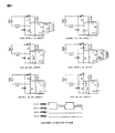
次に、図5から図9の等価回路に従って各動作モードの回路動作を説明する。図5に示すCモードは交流入力電圧Vinの絶対値が小さく、力率にはほとんど影響しない期間である。第3、第4のスイッチ素子Q3、Q4は、駆動損失を節約するためにオフ状態に保持されており、等価回路上には表記していない。交流電源Acinから正極性の電圧が出力される場合は、第1のスイッチ素子Q1を主スイッチ、第2のスイッチ素子Q2を同期整流素子、その逆に交流電源Acinから負極性の電圧が出力される場合は、第2のスイッチ素子Q2を主スイッチ、第1のスイッチ素子Q1を同期整流素子とする電流不連続モードのブーストコンバータに相似した電流が、交流電源Acinから流入するが、電流量は小さい。それ以外はエネルギー蓄積コンデンサCens1を入力源とする電流共振コンバータの動作と全く同じである。 Next, the circuit operation in each operation mode will be described in accordance with the equivalent circuits of FIGS. The C mode shown in FIG. 5 is a period in which the absolute value of the AC input voltage Vin is small and hardly affects the power factor. The third and fourth switch elements Q3 and Q4 are held in an off state in order to save drive loss, and are not shown on the equivalent circuit. When the positive voltage is output from the AC power source Acin, the first switch element Q1 is the main switch, the second switch element Q2 is the synchronous rectifier element, and conversely the negative voltage is output from the AC power source Acin. In this case, a current similar to a boost converter in a current discontinuous mode in which the second switch element Q2 is a main switch and the first switch element Q1 is a synchronous rectifier element flows from the AC power supply Acin. small. Other than that, the operation is the same as that of the current resonant converter using the energy storage capacitor Cens1 as an input source.
図5(a)においては、第2のスイッチ素子Q2と第1の同期整流素子SR1がオン状態で、第1のスイッチ素子Q1と第2の同期整流素子SR2がオフ状態であり、矢印で示した経路には共振インダクタLr1、共振コンデンサCr1の電流共振による正弦波状の電流が流れる。電流共振の半周期が終了すると、第1の同期整流素子SR1がターンオフして図5(b)の動作に移行する。 In FIG. 5A, the second switch element Q2 and the first synchronous rectifier element SR1 are in an on state, and the first switch element Q1 and the second synchronous rectifier element SR2 are in an off state, which are indicated by arrows. A sinusoidal current due to current resonance of the resonance inductor Lr1 and the resonance capacitor Cr1 flows through the path. When the half cycle of the current resonance ends, the first synchronous rectifier SR1 is turned off and the operation proceeds to the operation of FIG.
図5(b)においては、第2のスイッチ素子Q2がオン状態で、第1のスイッチ素子Q1、第1の同期整流素子SR1、第2の同期整流素子SR2がオフ状態であり、矢印で示した経路に共振インダクタLr1、トランスT1の励磁インダクタンスLm、共振コンデンサCr1の共振電流が流れる。第2のスイッチ素子Q2がターンオフすると、図5(b)の動作から図5(c)の動作に移行する。 In FIG. 5B, the second switch element Q2 is in the on state, and the first switch element Q1, the first synchronous rectifier element SR1, and the second synchronous rectifier element SR2 are in the off state, and are indicated by arrows. The resonant inductor Lr1, the exciting inductance Lm of the transformer T1, and the resonant current of the resonant capacitor Cr1 flow through the paths. When the second switch element Q2 is turned off, the operation of FIG. 5B shifts to the operation of FIG.
図5(c)においては、第1のスイッチ素子Q1、第2のスイッチ素子Q2、第1の同期整流素子SR1、第2の同期整流素子SR2が全てオフ状態であり、矢印で示した経路で電流が流れて、第1、第2のスイッチ素子Q1、Q2と並列に存在する寄生容量Cdisが充電される。寄生容量Cdisが充電されて第1のスイッチ素子Q1の両端電圧が0Vになった状態で第1のスイッチ素子Q1をターンオンすれば、ZVS(ゼロ電圧スイッチング)が達成され、図5(d)の動作に移行する。 In FIG. 5 (c), the first switch element Q1, the second switch element Q2, the first synchronous rectifier element SR1, and the second synchronous rectifier element SR2 are all in the off state, and the path indicated by the arrows. A current flows, and the parasitic capacitance Cdis existing in parallel with the first and second switch elements Q1 and Q2 is charged. If the first switch element Q1 is turned on in a state where the parasitic capacitance Cdis is charged and the voltage across the first switch element Q1 becomes 0V, ZVS (zero voltage switching) is achieved, as shown in FIG. Move to operation.
図5(d)においては、第1のスイッチ素子Q1と第2の同期整流素子SR2がオン状態で、第2のスイッチ素子Q2と第1の同期整流素子SR1がオフ状態であり、矢印で示した経路には共振インダクタLr1、共振コンデンサCr1の電流共振による正弦波状の電流が流れる。電流共振の半周期が終了すると、第2の同期整流素子SR2がターンオフして図5(e)の動作に移行する。 In FIG. 5D, the first switch element Q1 and the second synchronous rectifier element SR2 are in an on state, and the second switch element Q2 and the first synchronous rectifier element SR1 are in an off state, which are indicated by arrows. A sinusoidal current due to current resonance of the resonance inductor Lr1 and the resonance capacitor Cr1 flows through the path. When the half cycle of the current resonance is completed, the second synchronous rectifier SR2 is turned off and the operation proceeds to FIG.
図5(e)においては、第1のスイッチ素子Q1がオン状態で、第2のスイッチ素子Q2、第1の同期整流素子SR1、第2の同期整流素子SR2がオフ状態であり、矢印で示した共振インダクタLr1、トランスT1の励磁インダクタンスLm、共振コンデンサCr1の経路に共振電流が流れる。第1のスイッチ素子Q1がターンオフすると、図5(e)の動作から図5(f)の動作に移行する。 In FIG. 5 (e), the first switch element Q1 is in an on state, the second switch element Q2, the first synchronous rectifier element SR1, and the second synchronous rectifier element SR2 are in an off state, indicated by arrows. A resonance current flows through the path of the resonance inductor Lr1, the excitation inductance Lm of the transformer T1, and the resonance capacitor Cr1. When the first switch element Q1 is turned off, the operation of FIG. 5 (e) is shifted to the operation of FIG. 5 (f).
図5(f)においては、第1のスイッチ素子Q1、第2のスイッチ素子Q2、第1の同期整流素子SR1、第2の同期整流素子SR2が全てオフ状態であり、矢印で示した経路で電流が流れて、第1、第2のスイッチ素子Q1、Q2と並列に存在する寄生容量Cdisが放電される。寄生容量Cdisが放電されて第2のスイッチ素子Q2の両端電圧が0Vになった状態で第2のスイッチ素子Q2をターンオンすれば、ZVS(ゼロ電圧スイッチング)が達成され、再び、図5(a)の動作に移行する。前述の動作に従って、スイッチング動作が繰り返される。 In FIG. 5 (f), the first switch element Q1, the second switch element Q2, the first synchronous rectifier element SR1, and the second synchronous rectifier element SR2 are all in an off state, and are shown in the path indicated by the arrows. A current flows, and the parasitic capacitance Cdis existing in parallel with the first and second switch elements Q1 and Q2 is discharged. If the second switch element Q2 is turned on in a state where the parasitic capacitance Cdis is discharged and the voltage across the second switch element Q2 becomes 0V, ZVS (zero voltage switching) is achieved, and again FIG. ) The switching operation is repeated according to the above-described operation.
交流入力電圧Vinの正の半周期において、第1のスイッチ素子Q1がオンしている期間の1周期に対する比率、および交流入力電圧Vinの負の半周期において、第2のスイッチ素子Q2がオンしている期間の1周期に対する比率を第2のデューティ比D´と定義した場合、図5(g)に示す様に第2のデューティ比D´は0.5に保持され、周波数制御は、図5(b)と図5(e)に相当する期間の長さによって絶縁型DC−DCコンバータ部の入出力変換比を調整する。 In the positive half cycle of the AC input voltage Vin, the ratio of the period during which the first switch element Q1 is on to one cycle, and in the negative half cycle of the AC input voltage Vin, the second switch element Q2 is turned on. If the ratio of one period to one cycle is defined as the second duty ratio D ′, the second duty ratio D ′ is held at 0.5 as shown in FIG. The input / output conversion ratio of the isolated DC-DC converter unit is adjusted according to the length of the period corresponding to 5 (b) and FIG. 5 (e).
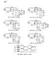
図6に示すA1モードは交流入力電圧Vinの正の半周期で、交流入力電圧Vinの絶対値がCモードの基準値より大きく、かつエネルギー蓄積コンデンサの両端電圧Vensの1/2以下の場合に相当する。A1モードの期間においては、PFC動作を行うために、第1のデューティ比D(整流/PFC回路部のデューティ比)は0.5以上の範囲でPWM制御されるが、第2のデューティ比D´は0.5に保持される。なお、A1モードにおいては、第4のスイッチ素子Q4は整流素子としてのみ作用するので、等価回路図にはダイオードとして表記している。 The A1 mode shown in FIG. 6 is a positive half cycle of the AC input voltage Vin, when the absolute value of the AC input voltage Vin is larger than the reference value of the C mode and less than 1/2 of the voltage Vens across the energy storage capacitor. Equivalent to. In the period of the A1 mode, in order to perform the PFC operation, the first duty ratio D (duty ratio of the rectification / PFC circuit unit) is PWM controlled within a range of 0.5 or more, but the second duty ratio D 'Is held at 0.5. In the A1 mode, the fourth switch element Q4 functions only as a rectifying element, and therefore is represented as a diode in the equivalent circuit diagram.
図6(a)においては、第1のスイッチ素子Q1、第3のスイッチ素子Q3、第2の同期整流素子SR2がオン状態で、第2のスイッチ素子Q2と第1の同期整流素子SR1がオフ状態である。A1モードにおける整流/PFC回路部は、第3のスイッチ素子Q3が主スイッチ、第2のスイッチ素子Q2が同期整流素子を成すブーストコンバータとして機能し、図6(a)では第3のスイッチ素子Q3がオン状態なので入力電流が漸増する。絶縁型DC−DCコンバータ部においては、エネルギー蓄積コンデンサCens1を入力源として矢印で示した共振インダクタLr1、共振コンデンサCr1の経路に電流共振による正弦波状の電流が流れる。電流共振の半周期が終了すると、第2の同期整流素子SR2がターンオフして図6(b)の動作に移行する。 In FIG. 6A, the first switch element Q1, the third switch element Q3, and the second synchronous rectifier element SR2 are in the on state, and the second switch element Q2 and the first synchronous rectifier element SR1 are in the off state. State. The rectification / PFC circuit unit in the A1 mode functions as a boost converter in which the third switch element Q3 forms a main switch and the second switch element Q2 forms a synchronous rectifier element. In FIG. 6A, the third switch element Q3 Since is on, the input current gradually increases. In the insulated DC-DC converter unit, a sinusoidal current due to current resonance flows through the path of the resonant inductor Lr1 and the resonant capacitor Cr1 indicated by arrows using the energy storage capacitor Cens1 as an input source. When the half cycle of the current resonance is completed, the second synchronous rectifier SR2 is turned off and the operation proceeds to the operation of FIG.
図6(b)においては、第1のスイッチ素子Q1と第3のスイッチ素子Q3がオン状態で、第2のスイッチ素子Q2、第1の同期整流素子SR1、第2の同期整流素子SR2がオフ状態である。整流/PFC回路部では第3のスイッチ素子Q3がオン状態なので引き続き入力電流が漸増する。第3、第4のスイッチ素子Q3、Q4の直列回路と並列に、第1の整流素子D1と第1のスイッチ素子Q1の直列回路が接続されているので、PFCインダクタLpfc1を流れる電流の一部は第1の整流素子D1と第1のスイッチ素子Q1の直列回路に分流し、導通損失が軽減される。絶縁型DC−DCコンバータ部においては、エネルギー蓄積コンデンサCens1を入力源として矢印で示した共振インダクタLr1、トランスT1の励磁インダクタンスLm、共振コンデンサCr1の経路に共振電流が流れる。第1のスイッチ素子Q1がターンオフすると、図6(b)の動作から図6(c)の動作に移行する。 In FIG. 6B, the first switch element Q1 and the third switch element Q3 are in the on state, and the second switch element Q2, the first synchronous rectifier element SR1, and the second synchronous rectifier element SR2 are off. State. In the rectification / PFC circuit portion, the third switch element Q3 is in the ON state, so that the input current gradually increases. Since the series circuit of the first rectifier element D1 and the first switch element Q1 is connected in parallel with the series circuit of the third and fourth switch elements Q3 and Q4, a part of the current flowing through the PFC inductor Lpfc1 Is shunted to the series circuit of the first rectifying element D1 and the first switching element Q1, and the conduction loss is reduced. In the insulated DC-DC converter unit, a resonance current flows through the path of the resonance inductor Lr1, the excitation inductance Lm of the transformer T1, and the resonance capacitor Cr1 indicated by an arrow with the energy storage capacitor Cens1 as an input source. When the first switch element Q1 is turned off, the operation of FIG. 6B shifts to the operation of FIG.
図6(c)においては、第3のスイッチ素子Q3がオン状態で、第1のスイッチ素子Q1、第2のスイッチ素子Q2、第1の同期整流素子SR1、第2の同期整流素子SR2がオフ状態である。整流/PFC回路部では第3のスイッチ素子Q3がオン状態なので引き続き入力電流が漸増する。絶縁型DC−DCコンバータ部においては、矢印で示した経路で電流が流れて、第1、第2のスイッチ素子Q1、Q2と並列に存在する寄生容量Cdisが放電される。寄生容量Cdisが放電されて第2のスイッチ素子Q2の両端電圧が0Vになった状態で第2のスイッチ素子Q2をターンオンすれば、ZVS(ゼロ電圧スイッチング)が達成され、図6(d)の動作に移行する。 In FIG. 6C, the third switch element Q3 is on, and the first switch element Q1, the second switch element Q2, the first synchronous rectifier element SR1, and the second synchronous rectifier element SR2 are off. State. In the rectification / PFC circuit portion, the third switch element Q3 is in the ON state, so that the input current gradually increases. In the insulated DC-DC converter unit, a current flows through a path indicated by an arrow, and the parasitic capacitance Cdis existing in parallel with the first and second switch elements Q1 and Q2 is discharged. If the second switch element Q2 is turned on in a state in which the parasitic capacitance Cdis is discharged and the voltage across the second switch element Q2 becomes 0V, ZVS (zero voltage switching) is achieved, and FIG. Move to operation.
図6(d)においては、第2のスイッチ素子Q2、第3のスイッチ素子Q3、第1の同期整流素子SR1がオン状態で、第1のスイッチ素子Q1と第2の同期整流素子SR2がオフ状態である。整流/PFC回路部では第3のスイッチ素子Q3がオン状態なので引き続き入力電流が漸増する。絶縁型DC−DCコンバータ部においては、矢印で示した共振インダクタLr1、共振コンデンサCr1の経路に電流共振による正弦波状の電流が流れる。図6(d)の期間において、第3のスイッチ素子Q3がターンオフすると整流/PFC回路部のブーストコンバータがオン状態からオフ状態に切り換わり、図6(e)の動作に移行する。 In FIG. 6D, the second switch element Q2, the third switch element Q3, and the first synchronous rectifier element SR1 are in the on state, and the first switch element Q1 and the second synchronous rectifier element SR2 are in the off state. State. In the rectification / PFC circuit portion, the third switch element Q3 is in the ON state, so that the input current gradually increases. In the insulated DC-DC converter section, a sinusoidal current due to current resonance flows through the path of the resonant inductor Lr1 and the resonant capacitor Cr1 indicated by arrows. In the period of FIG. 6D, when the third switch element Q3 is turned off, the boost converter of the rectification / PFC circuit unit is switched from the on state to the off state, and the operation shifts to the operation of FIG.
図6(e)においては、PFCインダクタLpfc1の電流は第1の整流素子D1、第2のスイッチ素子Q2を経由して、エネルギー蓄積コンデンサCens1を充電しながら漸減する。絶縁型DC−DCコンバータ部においては、引き続き、矢印で示した共振インダクタLr1、共振コンデンサCr1の経路に電流共振による正弦波状の電流が流れる。図6(e)の期間において、第2のスイッチ素子Q2は、整流/PFC回路部の同期整流素子としてソースからドレイン方向の電流が流れ込む一方で、絶縁型DC−DCコンバータ部の1次側ローサイドスイッチ素子としてドレインからソース方向の電流が流れ込む。互いに逆方向の電流が打ち消しあうため、第2のスイッチ素子Q2を流れる電流量が減少し、導通損失が減少する。電流共振の半周期が終了すると、第1の同期整流素子SR1がターンオフして図6(f)の動作に移行する。 In FIG. 6E, the current of the PFC inductor Lpfc1 gradually decreases while charging the energy storage capacitor Cens1 via the first rectifier element D1 and the second switch element Q2. In the insulated DC-DC converter unit, a sinusoidal current due to current resonance flows through the path of the resonant inductor Lr1 and the resonant capacitor Cr1 indicated by arrows. In the period of FIG. 6 (e), the second switch element Q2 has a current flowing from the source to the drain as a synchronous rectifier of the rectification / PFC circuit section, while the primary side of the isolated DC-DC converter section is low side. A current in the source direction flows from the drain as the switch element. Since currents in opposite directions cancel each other, the amount of current flowing through the second switch element Q2 is reduced, and conduction loss is reduced. When the half cycle of the current resonance is completed, the first synchronous rectifier SR1 is turned off and the operation proceeds to the operation of FIG.
図6(f)においては、第2のスイッチ素子Q2がオン状態で、第1のスイッチ素子Q1、第3のスイッチ素子Q3、第1の同期整流素子SR1、第2の同期整流素子SR2がオフ状態である。PFCインダクタLpfc1の電流は、引き続き、第1の整流素子D1、第2のスイッチ素子Q2を経由して、エネルギー蓄積コンデンサCens1を充電しながら漸減する。絶縁型DC−DCコンバータ部においては、矢印で示した、共振コンデンサCr1、トランスT1の励磁インダクタンスLm、共振インダクタLr1、第2のスイッチ素子Q2の経路に共振電流が流れる。図6(f)の期間においても、第2のスイッチ素子Q2は、整流/PFC回路部の同期整流素子としてソースからドレイン方向の電流が流れ込む一方で、絶縁型DC−DCコンバータ部の1次側ローサイドスイッチ素子としてドレインからソース方向の電流が流れ込む。互いに逆方向の電流が打ち消しあうため、第2のスイッチ素子Q2を流れる電流量が減少し、導通損失が減少する。図6(f)の期間において、第2のスイッチ素子Q2をターンオフすると同時に、第3のスイッチ素子Q3をターンオンすると図6(g)の動作に移行する。 In FIG. 6 (f), the second switch element Q2 is on, and the first switch element Q1, the third switch element Q3, the first synchronous rectifier element SR1, and the second synchronous rectifier element SR2 are off. State. The current of the PFC inductor Lpfc1 gradually decreases while charging the energy storage capacitor Cens1 via the first rectifier element D1 and the second switch element Q2. In the insulated DC-DC converter section, a resonance current flows through the path of the resonance capacitor Cr1, the exciting inductance Lm of the transformer T1, the resonance inductor Lr1, and the second switch element Q2 indicated by arrows. Also in the period of FIG. 6F, the second switch element Q2 has a current flowing from the source to the drain as a synchronous rectifier of the rectification / PFC circuit section, while the primary side of the isolated DC-DC converter section. A current in the source direction flows from the drain as the low-side switch element. Since currents in opposite directions cancel each other, the amount of current flowing through the second switch element Q2 is reduced, and conduction loss is reduced. In the period of FIG. 6 (f), when the second switch element Q2 is turned off and at the same time the third switch element Q3 is turned on, the operation shifts to the operation of FIG. 6 (g).
図6(g)においては、整流/PFC回路部のブーストコンバータはオフ状態からオン状態に切り換わり、入力電流が漸増する。絶縁型DC−DCコンバータ部においては、第1のスイッチ素子Q1、第2のスイッチ素子Q2、第1の同期整流素子SR1、第2の同期整流素子SR2が全てオフ状態であり、矢印で示した経路で電流が流れて、第1、第2のスイッチ素子Q1、Q2と並列に存在する寄生容量Cdisが充電される。寄生容量Cdisが充電されて第1のスイッチ素子Q1の両端電圧が0Vになった状態で第1のスイッチ素子Q1をターンオンすれば、ZVSが達成される。第1のスイッチ素子Q1をターンオンするより前のタイミングで第3のスイッチ素子Q3をターンオンする事によって、寄生容量Cdisの充電を妨げる方向の電流が流れなくなるので、ZVSが達成しやすくなる。第1のスイッチ素子Q1がターンオンすると、再び、図6(a)の動作に移行する。前述の動作に従って、スイッチング動作が繰り返される。 In FIG. 6G, the boost converter of the rectification / PFC circuit section switches from the off state to the on state, and the input current gradually increases. In the insulated DC-DC converter unit, the first switch element Q1, the second switch element Q2, the first synchronous rectifier element SR1, and the second synchronous rectifier element SR2 are all in an off state, and are indicated by arrows. A current flows through the path, and the parasitic capacitance Cdis existing in parallel with the first and second switch elements Q1 and Q2 is charged. If the first switch element Q1 is turned on in a state where the parasitic capacitance Cdis is charged and the voltage across the first switch element Q1 becomes 0V, ZVS is achieved. By turning on the third switch element Q3 at a timing before the first switch element Q1 is turned on, current in a direction that prevents charging of the parasitic capacitance Cdis does not flow, so that ZVS is easily achieved. When the first switch element Q1 is turned on, the operation again proceeds to the operation of FIG. The switching operation is repeated according to the above-described operation.
図6(h)に示す様に第2のデューティ比D´は0.5に保持され、第1のデューティ比D(整流/PFC回路部のデューティ比)は、PFC動作を行うために0.5以上の範囲でPWM制御される。周波数制御においては、図6(b)と図6(f)に相当する期間の長さによって絶縁型DC−DCコンバータ部の入出力変換比を調整する。 As shown in FIG. 6 (h), the second duty ratio D ′ is maintained at 0.5, and the first duty ratio D (duty ratio of the rectification / PFC circuit unit) is 0. 0 in order to perform the PFC operation. PWM control is performed in a range of 5 or more. In the frequency control, the input / output conversion ratio of the insulated DC-DC converter unit is adjusted according to the length of the period corresponding to FIGS. 6 (b) and 6 (f).
なお、図6(h)では、第4のスイッチ素子Q4のG−S間電圧はローレベル(オフ状態)に維持されているが、寄生ダイオードのみを利用しているのでG−S間電圧はハイレベル(オン状態)であっても良い。 In FIG. 6 (h), the GS voltage of the fourth switch element Q4 is maintained at a low level (off state). However, since only a parasitic diode is used, the GS voltage is It may be at a high level (on state).
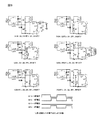
図7に示すA2モードは交流入力電圧Vinの正の半周期で、交流入力電圧Vinの絶対値がエネルギー蓄積コンデンサの両端電圧Vensの1/2より大きい場合に相当する。A2モードは全ての交流入力電圧範囲で発生するわけではなく、例えばエネルギー蓄積コンデンサの両端電圧Vensを400Vに設定すると、交流電圧の実効値が140V以下だとA2モードは発生しない。A2モードの期間においては、PFC動作を行うために、第1のデューティ比D(整流/PFC回路部のデューティ比)は0.5より小さい範囲でPWM制御され、それに応じて第2のデューティ比D´も第1のデューティ比Dと実質的に等しい値となり、PWM制御される。なお、A2モードにおいても、第4のスイッチ素子Q4は整流素子としてのみ作用するので、等価回路図にはダイオードとして表記している。 The A2 mode shown in FIG. 7 corresponds to a case where the AC input voltage Vin is a positive half cycle and the absolute value of the AC input voltage Vin is larger than ½ of the voltage Vens across the energy storage capacitor. The A2 mode does not occur in the entire AC input voltage range. For example, when the voltage Vens across the energy storage capacitor is set to 400 V, the A2 mode does not occur when the effective value of the AC voltage is 140 V or less. In the period of the A2 mode, in order to perform the PFC operation, the first duty ratio D (duty ratio of the rectification / PFC circuit unit) is PWM controlled within a range smaller than 0.5, and the second duty ratio is accordingly adjusted. D ′ is also substantially equal to the first duty ratio D, and is PWM controlled. Even in the A2 mode, the fourth switch element Q4 acts only as a rectifying element, and therefore is represented as a diode in the equivalent circuit diagram.
図7(a)においては、第1のスイッチ素子Q1、第3のスイッチ素子Q3、第2の同期整流素子SR2がオン状態で、第2のスイッチ素子Q2と第1の同期整流素子SR1がオフ状態である。A2モードにおける整流/PFC回路部は、第1のスイッチ素子Q1と第3のスイッチ素子Q3とが主スイッチ、第2のスイッチ素子Q2が同期整流素子を成すブーストコンバータとして機能し、図7(a)では第1のスイッチ素子Q1と第3のスイッチ素子Q3がオン状態なので入力電流が漸増する。絶縁型DC−DCコンバータ部においては、エネルギー蓄積コンデンサCens1を入力源として矢印で示した共振インダクタLr1、共振コンデンサCr1の経路に電流共振による正弦波状の電流が流れる。電流共振の半周期が終了すると、第2の同期整流素子SR2がターンオフして図7(b)の動作に移行する。 In FIG. 7A, the first switch element Q1, the third switch element Q3, and the second synchronous rectifier element SR2 are on, and the second switch element Q2 and the first synchronous rectifier element SR1 are off. State. The rectification / PFC circuit unit in the A2 mode functions as a boost converter in which the first switch element Q1 and the third switch element Q3 form a main switch and the second switch element Q2 forms a synchronous rectifier element. ), Since the first switch element Q1 and the third switch element Q3 are in the ON state, the input current gradually increases. In the insulated DC-DC converter unit, a sinusoidal current due to current resonance flows through the path of the resonant inductor Lr1 and the resonant capacitor Cr1 indicated by arrows using the energy storage capacitor Cens1 as an input source. When the half cycle of the current resonance is completed, the second synchronous rectifier SR2 is turned off and the operation proceeds to the operation of FIG.
図7(b)においては、第1のスイッチ素子Q1と第3のスイッチ素子Q3がオン状態で、第2のスイッチ素子Q2、第1の同期整流素子SR1、第2の同期整流素子SR2がオフ状態である。整流/PFC回路部では第1のスイッチ素子Q1と第3のスイッチ素子Q3がオン状態なので引き続き入力電流が漸増する。図7(b)においては、絶縁型DC−DCコンバータ部から第1のスイッチ素子Q1に流れ込む電流による電圧降下が比較的小さいので、PFCインダクタLpfc1を流れる電流の一部は第1の整流素子D1と第1のスイッチ素子Q1の直列回路に分流し、導通損失が軽減される。絶縁型DC−DCコンバータ部においては、エネルギー蓄積コンデンサCens1を入力源として矢印で示した共振インダクタLr1、トランスT1の励磁インダクタンスLm、共振コンデンサCr1の経路に共振電流が流れる。第1のスイッチ素子Q1と第3のスイッチ素子Q3を同時にターンオフすると、図7(b)の動作から図7(c)の動作に移行する。 In FIG. 7B, the first switch element Q1 and the third switch element Q3 are on, and the second switch element Q2, the first synchronous rectifier element SR1, and the second synchronous rectifier element SR2 are off. State. In the rectification / PFC circuit section, the first switch element Q1 and the third switch element Q3 are in the ON state, so that the input current continues to increase gradually. In FIG. 7B, since the voltage drop due to the current flowing into the first switch element Q1 from the insulated DC-DC converter section is relatively small, a part of the current flowing through the PFC inductor Lpfc1 is the first rectifier element D1. And the first switch element Q1 are shunted to reduce the conduction loss. In the insulated DC-DC converter unit, a resonance current flows through the path of the resonance inductor Lr1, the excitation inductance Lm of the transformer T1, and the resonance capacitor Cr1 indicated by an arrow with the energy storage capacitor Cens1 as an input source. When the first switch element Q1 and the third switch element Q3 are turned off simultaneously, the operation shown in FIG. 7B is shifted to the operation shown in FIG. 7C.
図7(c)においては、第1のスイッチ素子Q1、第2のスイッチ素子Q2、第3のスイッチ素子Q3、第1の同期整流素子SR1、第2の同期整流素子SR2が全てオフ状態である。整流/PFC回路部のブーストコンバータがオン状態からオフ状態に切り換わる。PFCインダクタLpfc1の電流と絶縁型DC−DCコンバータ部の矢印で示した経路の電流によって、第1、第2のスイッチ素子Q1、Q2と並列に存在する寄生容量Cdisが放電される。寄生容量Cdisが放電されて第2のスイッチ素子Q2の両端電圧が0Vになった状態で第2のスイッチ素子Q2をターンオンすれば、ZVS(ゼロ電圧スイッチング)が達成され、図7(d)の動作に移行する。 In FIG. 7C, the first switch element Q1, the second switch element Q2, the third switch element Q3, the first synchronous rectifier element SR1, and the second synchronous rectifier element SR2 are all in an OFF state. . The boost converter of the rectification / PFC circuit unit switches from the on state to the off state. The parasitic capacitance Cdis existing in parallel with the first and second switch elements Q1 and Q2 is discharged by the current of the PFC inductor Lpfc1 and the current of the path indicated by the arrow of the insulated DC-DC converter unit. If the second switch element Q2 is turned on in a state in which the parasitic capacitance Cdis is discharged and the voltage across the second switch element Q2 becomes 0V, ZVS (zero voltage switching) is achieved, and FIG. Move to operation.
図7(d)においては、第2のスイッチ素子Q2と第1の同期整流素子SR1がオン状態で、第1のスイッチ素子Q1、第3のスイッチ素子Q3、第2の同期整流素子SR2がオフ状態である。PFCインダクタLpfc1の電流は第1の整流素子D1、第2のスイッチ素子Q2を経由して、エネルギー蓄積コンデンサCens1を充電しながら漸減する。絶縁型DC−DCコンバータ部においては、矢印で示した共振インダクタLr1、共振コンデンサCr1の経路に電流共振による正弦波状の電流が流れる。図7(d)の期間において、第2のスイッチ素子Q2は、整流/PFC回路部の同期整流素子としてソースからドレイン方向の電流が流れ込む一方で、絶縁型DC−DCコンバータ部の1次側ローサイドスイッチ素子としてドレインからソース方向の電流が流れ込む。互いに逆方向の電流が打ち消しあうため、第2のスイッチ素子Q2を流れる電流量が減少し、導通損失が減少する。電流共振の半周期が終了すると、第1の同期整流素子SR1がターンオフして図7(e)の動作に移行する。 In FIG. 7D, the second switch element Q2 and the first synchronous rectifier element SR1 are in the on state, and the first switch element Q1, the third switch element Q3, and the second synchronous rectifier element SR2 are off. State. The current of the PFC inductor Lpfc1 gradually decreases while charging the energy storage capacitor Cens1 via the first rectifier element D1 and the second switch element Q2. In the insulated DC-DC converter section, a sinusoidal current due to current resonance flows through the path of the resonant inductor Lr1 and the resonant capacitor Cr1 indicated by arrows. In the period of FIG. 7D, the second switch element Q2 has a current flowing from the source to the drain as a synchronous rectifier element of the rectification / PFC circuit section, while the primary low side of the isolated DC-DC converter section. A current in the source direction flows from the drain as the switch element. Since currents in opposite directions cancel each other, the amount of current flowing through the second switch element Q2 is reduced, and conduction loss is reduced. When the half cycle of the current resonance is completed, the first synchronous rectifying element SR1 is turned off and the operation proceeds to the operation of FIG.
図7(e)においては、第2のスイッチ素子Q2がオン状態で、第1のスイッチ素子Q1、第3のスイッチ素子Q3、第1の同期整流素子SR1、第2の同期整流素子SR2がオフ状態である。PFCインダクタLpfc1の電流は、引き続き、第1の整流素子D1、第2のスイッチ素子Q2を経由して、エネルギー蓄積コンデンサCens1を充電しながら漸減する。絶縁型DC−DCコンバータ部においては、矢印で示した、共振コンデンサCr1、トランスT1の励磁インダクタンスLm、共振インダクタLr1、第2のスイッチ素子Q2の経路に共振電流が流れる。図7(e)の期間においても、第2のスイッチ素子Q2は、整流/PFC回路部の同期整流素子としてソースからドレイン方向の電流が流れ込む一方で、絶縁型DC−DCコンバータ部の1次側ローサイドスイッチ素子としてドレインからソース方向の電流が流れ込む。互いに逆方向の電流が打ち消しあうため、第2のスイッチ素子Q2を流れる電流量が減少し、導通損失が減少する。図7(e)の期間において、第2のスイッチ素子Q2をターンオフすると同時に、第3のスイッチ素子Q3をターンオンすると図7(f)の動作に移行する。 In FIG. 7E, the second switch element Q2 is in the on state, and the first switch element Q1, the third switch element Q3, the first synchronous rectifier element SR1, and the second synchronous rectifier element SR2 are off. State. The current of the PFC inductor Lpfc1 gradually decreases while charging the energy storage capacitor Cens1 via the first rectifier element D1 and the second switch element Q2. In the insulated DC-DC converter section, a resonance current flows through the path of the resonance capacitor Cr1, the exciting inductance Lm of the transformer T1, the resonance inductor Lr1, and the second switch element Q2 indicated by arrows. Even during the period of FIG. 7 (e), the second switch element Q2 has a current flowing from the source to the drain as a synchronous rectifier of the rectification / PFC circuit section, while the primary side of the isolated DC-DC converter section. A current in the source direction flows from the drain as the low-side switch element. Since currents in opposite directions cancel each other, the amount of current flowing through the second switch element Q2 is reduced, and conduction loss is reduced. When the second switch element Q2 is turned off and the third switch element Q3 is turned on simultaneously with the period of FIG. 7E, the operation shifts to the operation of FIG.
図7(f)においては、第3のスイッチ素子Q3がオン状態であり、第1のスイッチ素子Q1、第2のスイッチ素子Q2、第1の同期整流素子SR1、第2の同期整流素子SR2はオフ状態である。整流/PFC回路部のブーストコンバータがオフ状態からオン状態に切り換わるので、入力電流は漸増する。絶縁型DC−DCコンバータ部においては、矢印で示した経路で電流が流れて、第1、第2のスイッチ素子Q1、Q2と並列に存在する寄生容量Cdisが充電される。寄生容量Cdisが充電されて第1のスイッチ素子Q1の両端電圧が0Vになった状態で第1のスイッチ素子Q1をターンオンすれば、ZVSが達成される。第1のスイッチ素子Q1をターンオンするより前のタイミングで第3のスイッチ素子Q3をターンオンする事によって、寄生容量Cdisの充電を妨げる方向の電流が流れなくなるので、ZVSが達成しやすくなる。第1のスイッチ素子Q1がターンオンすると、再び、図7(a)の動作に移行する。前述の動作に従って、スイッチング動作が繰り返される。 In FIG. 7F, the third switch element Q3 is in the ON state, and the first switch element Q1, the second switch element Q2, the first synchronous rectifier element SR1, and the second synchronous rectifier element SR2 are Off state. Since the boost converter of the rectification / PFC circuit section switches from the off state to the on state, the input current gradually increases. In the insulated DC-DC converter unit, a current flows through a path indicated by an arrow, and the parasitic capacitance Cdis existing in parallel with the first and second switch elements Q1 and Q2 is charged. If the first switch element Q1 is turned on in a state where the parasitic capacitance Cdis is charged and the voltage across the first switch element Q1 becomes 0V, ZVS is achieved. By turning on the third switch element Q3 at a timing before the first switch element Q1 is turned on, current in a direction that prevents charging of the parasitic capacitance Cdis does not flow, so that ZVS is easily achieved. When the first switch element Q1 is turned on, the operation again proceeds to the operation of FIG. The switching operation is repeated according to the above-described operation.
図7(g)に示す様に第1のデューティ比D(整流/PFC回路部のデューティ比)と第2のデューティ比D´は実質的に同じ値となり、PFC動作を行うために第1のデューティ比Dを0.5より小さい範囲でPWM制御すると、それに伴って第2のデューティ比D´もPWM制御される。周波数制御においては、図7(b)と図7(e)に相当する期間の長さによって絶縁型DC−DCコンバータ部の入出力変換比を調整する。 As shown in FIG. 7 (g), the first duty ratio D (duty ratio of the rectification / PFC circuit portion) and the second duty ratio D ′ are substantially the same value, and the first duty ratio D ' When the PWM control is performed in a range where the duty ratio D is smaller than 0.5, the second duty ratio D ′ is also PWM controlled accordingly. In the frequency control, the input / output conversion ratio of the insulated DC-DC converter unit is adjusted according to the length of the period corresponding to FIGS. 7B and 7E.
なお、図7(g)では、第4のスイッチ素子Q4のG−S間電圧はローレベル(オフ状態)に維持されているが、寄生ダイオードのみを利用しているのでG−S間電圧はハイレベル(オン状態)であっても良い。 In FIG. 7G, the GS voltage of the fourth switch element Q4 is maintained at a low level (off state), but only the parasitic diode is used, so the GS voltage is It may be at a high level (on state).
図8に示すB1モードは交流入力電圧Vinの負の半周期で、交流入力電圧Vinの絶対値がCモードの基準値より大きく、かつエネルギー蓄積コンデンサの両端電圧Vensの1/2以下の場合に相当する。B1モードでは、A1モードと相似した回路動作になるが、第1の整流素子D1と第2の整流素子D2、第1のスイッチ素子Q1と第2のスイッチ素子Q2、第3のスイッチ素子Q3と第4のスイッチ素子Q4、第1の同期整流素子SR1と第2の同期整流素子SR2、とは互いの役割が入れかわる。B1モードの期間においては、PFC動作を行うために、第1のデューティ比D(整流/PFC回路部のデューティ比)は0.5以上の範囲でPWM制御されるが、第2のデューティ比D´は0.5に保持される。なお、B1モードにおいては、第3のスイッチ素子Q3は整流素子としてのみ作用するので、等価回路図にはダイオードとして表記している。 The B1 mode shown in FIG. 8 is a negative half cycle of the AC input voltage Vin, and the absolute value of the AC input voltage Vin is larger than the reference value of the C mode and is less than or equal to 1/2 of the voltage Vens across the energy storage capacitor. Equivalent to. In the B1 mode, the circuit operation is similar to that of the A1 mode, but the first rectifier element D1, the second rectifier element D2, the first switch element Q1, the second switch element Q2, the third switch element Q3, The roles of the fourth switch element Q4, the first synchronous rectifier element SR1, and the second synchronous rectifier element SR2 are interchanged. In the period of the B1 mode, in order to perform the PFC operation, the first duty ratio D (duty ratio of the rectification / PFC circuit unit) is PWM controlled within a range of 0.5 or more, but the second duty ratio D 'Is held at 0.5. In the B1 mode, the third switch element Q3 acts only as a rectifying element, and therefore is represented as a diode in the equivalent circuit diagram.
図8(a)においては、第2のスイッチ素子Q2、第4のスイッチ素子Q4、第1の同期整流素子SR1がオン状態で、第1のスイッチ素子Q1と第2の同期整流素子SR2がオフ状態である。B1モードにおける整流/PFC回路部は、第4のスイッチ素子Q4が主スイッチ、第1のスイッチ素子Q1が同期整流素子を成すブーストコンバータとして機能し、図8(a)では第4のスイッチ素子Q4がオン状態なので入力電流が漸増する。絶縁型DC−DCコンバータ部においては、矢印で示した共振コンデンサCr1、共振インダクタLr1の経路に電流共振による正弦波状の電流が流れる。電流共振の半周期が終了すると、第1の同期整流素子SR1がターンオフして図8(b)の動作に移行する。 In FIG. 8A, the second switch element Q2, the fourth switch element Q4, and the first synchronous rectifier element SR1 are on, and the first switch element Q1 and the second synchronous rectifier element SR2 are off. State. The rectification / PFC circuit unit in the B1 mode functions as a boost converter in which the fourth switch element Q4 forms a main switch and the first switch element Q1 forms a synchronous rectifier element. In FIG. 8A, the fourth switch element Q4 Since is on, the input current gradually increases. In the insulated DC-DC converter section, a sinusoidal current due to current resonance flows through the path of the resonance capacitor Cr1 and the resonance inductor Lr1 indicated by arrows. When the half cycle of the current resonance is completed, the first synchronous rectifying element SR1 is turned off and the operation proceeds to the operation of FIG.
図8(b)においては、第2のスイッチ素子Q2と第4のスイッチ素子Q4がオン状態で、第1のスイッチ素子Q1、第1の同期整流素子SR1、第2の同期整流素子SR2がオフ状態である。整流/PFC回路部では第4のスイッチ素子Q4がオン状態なので引き続き入力電流が漸増する。第3、第4のスイッチ素子Q3、Q4の直列回路と並列に、第2の整流素子D2と第2のスイッチ素子Q2の直列回路が接続されているので、PFCインダクタLpfc1を流れる電流の一部は第2の整流素子D2と第2のスイッチ素子Q2の直列回路に分流し、導通損失が軽減される。絶縁型DC−DCコンバータ部においては、矢印で示した共振コンデンサCr1、トランスT1の励磁インダクタンスLm、共振インダクタLr1、第2のスイッチ素子Q2の経路に共振電流が流れる。第2のスイッチ素子Q2がターンオフすると、図8(b)の動作から図8(c)の動作に移行する。 In FIG. 8B, the second switch element Q2 and the fourth switch element Q4 are in the on state, and the first switch element Q1, the first synchronous rectifier element SR1, and the second synchronous rectifier element SR2 are off. State. In the rectification / PFC circuit portion, the fourth switch element Q4 is in the ON state, so that the input current gradually increases. Since the series circuit of the second rectifier element D2 and the second switch element Q2 is connected in parallel with the series circuit of the third and fourth switch elements Q3 and Q4, a part of the current flowing through the PFC inductor Lpfc1 Is shunted to the series circuit of the second rectifier element D2 and the second switch element Q2, and the conduction loss is reduced. In the insulated DC-DC converter section, a resonance current flows through the path of the resonance capacitor Cr1, the excitation inductance Lm of the transformer T1, the resonance inductor Lr1, and the second switch element Q2 indicated by arrows. When the second switch element Q2 is turned off, the operation of FIG. 8B shifts to the operation of FIG.
図8(c)においては、第4のスイッチ素子Q4がオン状態で、第1のスイッチ素子Q1、第2のスイッチ素子Q2、第1の同期整流素子SR1、第2の同期整流素子SR2がオフ状態である。整流/PFC回路部では第4のスイッチ素子Q4がオン状態なので引き続き入力電流が漸増する。絶縁型DC−DCコンバータ部においては、矢印で示した経路で電流が流れて、第1、第2のスイッチ素子Q1、Q2と並列に存在する寄生容量Cdisが充電される。寄生容量Cdisが充電されて第1のスイッチ素子Q1の両端電圧が0Vになった状態で第1のスイッチ素子Q1をターンオンすれば、ZVS(ゼロ電圧スイッチング)が達成され、図8(d)の動作に移行する。 In FIG. 8C, the fourth switch element Q4 is in the on state, and the first switch element Q1, the second switch element Q2, the first synchronous rectifier element SR1, and the second synchronous rectifier element SR2 are off. State. In the rectification / PFC circuit portion, the fourth switch element Q4 is in the ON state, so that the input current gradually increases. In the insulated DC-DC converter unit, a current flows through a path indicated by an arrow, and the parasitic capacitance Cdis existing in parallel with the first and second switch elements Q1 and Q2 is charged. If the first switch element Q1 is turned on in a state where the parasitic capacitance Cdis is charged and the voltage across the first switch element Q1 becomes 0V, ZVS (zero voltage switching) is achieved, as shown in FIG. Move to operation.
図8(d)においては、第1のスイッチ素子Q1、第4のスイッチ素子Q4、第2の同期整流素子SR2がオン状態で、第2のスイッチ素子Q2と第1の同期整流素子SR1がオフ状態である。整流/PFC回路部では第4のスイッチ素子Q4がオン状態なので引き続き入力電流が漸増する。絶縁型DC−DCコンバータ部においては、エネルギー蓄積コンデンサCens1を入力源として矢印で示した共振インダクタLr1、共振コンデンサCr1の経路に電流共振による正弦波状の電流が流れる。図8(d)の期間において、第4のスイッチ素子Q4がターンオフすると整流/PFC回路部のブーストコンバータがオン状態からオフ状態に切り換わり、図8(e)の動作に移行する。 In FIG. 8D, the first switch element Q1, the fourth switch element Q4, and the second synchronous rectifier element SR2 are on, and the second switch element Q2 and the first synchronous rectifier element SR1 are off. State. In the rectification / PFC circuit portion, the fourth switch element Q4 is in the ON state, so that the input current gradually increases. In the insulated DC-DC converter unit, a sinusoidal current due to current resonance flows through the path of the resonant inductor Lr1 and the resonant capacitor Cr1 indicated by arrows using the energy storage capacitor Cens1 as an input source. In the period of FIG. 8D, when the fourth switch element Q4 is turned off, the boost converter of the rectification / PFC circuit unit is switched from the on state to the off state, and the operation shifts to the operation of FIG.
図8(e)においては、PFCインダクタLpfc1の電流は第2の整流素子D2、第1のスイッチ素子Q1を経由して、エネルギー蓄積コンデンサCens1を充電しながら漸減する。絶縁型DC−DCコンバータ部においては、引き続き、エネルギー蓄積コンデンサCens1を入力源として矢印で示した共振インダクタLr1、共振コンデンサCr1の経路に電流共振による正弦波状の電流が流れる。図8(e)の期間において、第1のスイッチ素子Q1は、整流/PFC回路部の同期整流素子としてソースからドレイン方向の電流が流れ込む一方で、絶縁型DC−DCコンバータ部の1次側ハイサイドスイッチ素子としてドレインからソース方向の電流が流れ込む。互いに逆方向の電流が打ち消しあうため、第1のスイッチ素子Q1を流れる電流量が減少し、導通損失が減少する。電流共振の半周期が終了すると、第2の同期整流素子SR2がターンオフして図8(f)の動作に移行する。 In FIG. 8E, the current of the PFC inductor Lpfc1 gradually decreases while charging the energy storage capacitor Cens1 via the second rectifier element D2 and the first switch element Q1. In the isolated DC-DC converter unit, a sine wave current due to current resonance flows through the path of the resonant inductor Lr1 and the resonant capacitor Cr1 indicated by arrows using the energy storage capacitor Cens1 as an input source. In the period of FIG. 8 (e), the first switch element Q1 has a current flowing from the source to the drain as a synchronous rectifier element of the rectification / PFC circuit section, while the primary side of the isolated DC-DC converter section is high. A current in the source direction flows from the drain as the side switch element. Since currents in opposite directions cancel each other, the amount of current flowing through the first switch element Q1 is reduced, and conduction loss is reduced. When the half cycle of the current resonance ends, the second synchronous rectifier SR2 is turned off and the operation proceeds to the operation of FIG.
図8(f)においては、第1のスイッチ素子Q1がオン状態で、第2のスイッチ素子Q2、第4のスイッチ素子Q4、第1の同期整流素子SR1、第2の同期整流素子SR2がオフ状態である。PFCインダクタLpfc1の電流は、引き続き、第2の整流素子D2、第1のスイッチ素子Q1を経由して、エネルギー蓄積コンデンサCens1を充電しながら漸減する。絶縁型DC−DCコンバータ部においては、エネルギー蓄積コンデンサCens1を入力源として矢印で示した第1のスイッチ素子Q1、共振インダクタLr1、トランスT1の励磁インダクタンスLm、共振コンデンサCr1の経路に共振電流が流れる。図8(f)の期間においても、第1のスイッチ素子Q1は、整流/PFC回路部の同期整流素子としてソースからドレイン方向の電流が流れ込む一方で、絶縁型DC−DCコンバータ部の1次側ハイサイドスイッチ素子としてドレインからソース方向の電流が流れ込む。互いに逆方向の電流が打ち消しあうため、第1のスイッチ素子Q1を流れる電流量が減少し、導通損失が減少する。図8(f)の期間において、第1のスイッチ素子Q1をターンオフすると同時に、第4のスイッチ素子Q4をターンオンすると図8(g)の動作に移行する。 In FIG. 8F, the first switch element Q1 is in the on state, and the second switch element Q2, the fourth switch element Q4, the first synchronous rectifier element SR1, and the second synchronous rectifier element SR2 are off. State. The current of the PFC inductor Lpfc1 continues to gradually decrease while charging the energy storage capacitor Cens1 via the second rectifier element D2 and the first switch element Q1. In the insulated DC-DC converter unit, a resonance current flows through the path of the first switch element Q1, the resonance inductor Lr1, the excitation inductance Lm of the transformer T1, and the resonance capacitor Cr1 indicated by arrows using the energy storage capacitor Cens1 as an input source. . Also in the period of FIG. 8 (f), the first switch element Q1 has a current flowing from the source to the drain as a synchronous rectifier of the rectification / PFC circuit section, while the primary side of the isolated DC-DC converter section. A current in the source direction flows from the drain as the high-side switch element. Since currents in opposite directions cancel each other, the amount of current flowing through the first switch element Q1 is reduced, and conduction loss is reduced. In the period of FIG. 8F, when the first switch element Q1 is turned off and the fourth switch element Q4 is turned on, the operation shown in FIG. 8G is started.
図8(g)においては、整流/PFC回路部のブーストコンバータはオフ状態からオン状態に切り換わり、入力電流が漸増する。絶縁型DC−DCコンバータ部においては、第1のスイッチ素子Q1、第2のスイッチ素子Q2、第1の同期整流素子SR1、第2の同期整流素子SR2が全てオフ状態であり、矢印で示した経路で電流が流れて、第1、第2のスイッチ素子Q1、Q2と並列に存在する寄生容量Cdisが放電される。寄生容量Cdisが放電されて第2のスイッチ素子Q2の両端電圧が0Vになった状態で第2のスイッチ素子Q2をターンオンすれば、ZVSが達成される。第2のスイッチ素子Q2をターンオンするより前のタイミングで第4のスイッチ素子Q4をターンオンする事によって、寄生容量Cdisの放電を妨げる方向の電流が流れなくなるので、ZVSが達成しやすくなる。第2のスイッチ素子Q2がターンオンすると、再び、図8(a)の動作に移行する。前述の動作に従って、スイッチング動作が繰り返される。 In FIG. 8G, the boost converter of the rectification / PFC circuit section is switched from the off state to the on state, and the input current gradually increases. In the insulated DC-DC converter unit, the first switch element Q1, the second switch element Q2, the first synchronous rectifier element SR1, and the second synchronous rectifier element SR2 are all in an off state, and are indicated by arrows. A current flows through the path, and the parasitic capacitance Cdis existing in parallel with the first and second switch elements Q1 and Q2 is discharged. If the second switch element Q2 is turned on in a state where the parasitic capacitance Cdis is discharged and the voltage across the second switch element Q2 becomes 0V, ZVS is achieved. By turning on the fourth switch element Q4 at a timing before turning on the second switch element Q2, no current flows in a direction that prevents the discharge of the parasitic capacitance Cdis, so that ZVS is easily achieved. When the second switch element Q2 is turned on, the operation again proceeds to the operation of FIG. The switching operation is repeated according to the above-described operation.
図8(h)に示す様に第2のデューティ比D´は0.5に保持され、第1のデューティ比D(整流/PFC回路部のデューティ比)は、PFC動作を行うために0.5以上の範囲でPWM制御される。周波数制御においては、図8(b)と図8(f)に相当する期間の長さによって絶縁型DC−DCコンバータ部の入出力変換比を調整する。 As shown in FIG. 8H, the second duty ratio D ′ is held at 0.5, and the first duty ratio D (duty ratio of the rectification / PFC circuit unit) is set to 0. 0 to perform the PFC operation. PWM control is performed in a range of 5 or more. In the frequency control, the input / output conversion ratio of the insulated DC-DC converter unit is adjusted according to the length of the period corresponding to FIGS. 8B and 8F.
なお、図8(h)では、第3のスイッチ素子Q3のG−S間電圧はローレベル(オフ状態)に維持されているが、寄生ダイオードのみを利用しているのでG−S間電圧はハイレベル(オン状態)であっても良い。 In FIG. 8 (h), the GS voltage of the third switch element Q3 is maintained at a low level (off state). However, since only a parasitic diode is used, the GS voltage is It may be at a high level (on state).
図9に示すB2モードは交流入力電圧Vinの負の半周期で、交流入力電圧Vinの絶対値がエネルギー蓄積コンデンサの両端電圧Vensの1/2より大きい場合に相当する。B2モードの期間においては、PFC動作を行うために、第1のデューティ比D(整流/PFC回路部のデューティ比)は0.5より小さい範囲でPWM制御され、それに応じて第2のデューティ比D´も第1のデューティ比Dと実質的に等しい値となり、PWM制御される。B2モードでは、A2モードと相似した回路動作になるが、第1の整流素子D1と第2の整流素子D2、第1のスイッチ素子Q1と第2のスイッチ素子Q2、第3のスイッチ素子Q3と第4のスイッチ素子Q4、第1の同期整流素子SR1と第2の同期整流素子SR2、とは互いの役割が入れかわる。B2モードにおいては、第3のスイッチ素子Q3は整流素子としてのみ作用するので、等価回路図にはダイオードとして表記している。なお、B2モードは全ての交流入力電圧範囲で発生するわけではなく、例えばエネルギー蓄積コンデンサの両端電圧Vensを400Vに設定すると、交流電圧の実効値が140V以下だとB2モードは発生しない。 The B2 mode shown in FIG. 9 corresponds to the case where the AC input voltage Vin is a negative half cycle and the absolute value of the AC input voltage Vin is larger than ½ of the voltage Vens across the energy storage capacitor. In the period of the B2 mode, in order to perform the PFC operation, the first duty ratio D (duty ratio of the rectification / PFC circuit unit) is PWM controlled within a range smaller than 0.5, and the second duty ratio is accordingly adjusted. D ′ is also substantially equal to the first duty ratio D, and is PWM controlled. In the B2 mode, the circuit operation is similar to the A2 mode, but the first rectifier element D1, the second rectifier element D2, the first switch element Q1, the second switch element Q2, the third switch element Q3, The roles of the fourth switch element Q4, the first synchronous rectifier element SR1, and the second synchronous rectifier element SR2 are interchanged. In the B2 mode, the third switching element Q3 acts only as a rectifying element, and therefore is represented as a diode in the equivalent circuit diagram. The B2 mode does not occur in the entire AC input voltage range. For example, when the voltage Vens across the energy storage capacitor is set to 400 V, the B2 mode does not occur if the effective value of the AC voltage is 140 V or less.
図9(a)においては、第2のスイッチ素子Q2、第4のスイッチ素子Q4、第1の同期整流素子SR1がオン状態で、第1のスイッチ素子Q1と第2の同期整流素子SR2がオフ状態である。B2モードにおける整流/PFC回路部は、第2のスイッチ素子Q2と第4のスイッチ素子Q4とが主スイッチ、第1のスイッチ素子Q1が同期整流素子を成すブーストコンバータとして機能し、図9(a)では第2のスイッチ素子Q2と第4のスイッチ素子Q4がオン状態なので入力電流が漸増する。絶縁型DC−DCコンバータ部においては、矢印で示した共振インダクタLr1、共振コンデンサCr1の経路に電流共振による正弦波状の電流が流れる。電流共振の半周期が終了すると、第1の同期整流素子SR1がターンオフして図9(b)の動作に移行する。 In FIG. 9A, the second switch element Q2, the fourth switch element Q4, and the first synchronous rectifier element SR1 are on, and the first switch element Q1 and the second synchronous rectifier element SR2 are off. State. The rectification / PFC circuit section in the B2 mode functions as a boost converter in which the second switch element Q2 and the fourth switch element Q4 form a main switch and the first switch element Q1 forms a synchronous rectifier element. ), Since the second switch element Q2 and the fourth switch element Q4 are in the ON state, the input current gradually increases. In the insulated DC-DC converter section, a sinusoidal current due to current resonance flows through the path of the resonant inductor Lr1 and the resonant capacitor Cr1 indicated by arrows. When the half cycle of the current resonance is completed, the first synchronous rectifier SR1 is turned off and the operation proceeds to the operation of FIG.
図9(b)においては、第2のスイッチ素子Q2と第4のスイッチ素子Q4がオン状態で、第1のスイッチ素子Q1、第1の同期整流素子SR1、第2の同期整流素子SR2がオフ状態である。整流/PFC回路部では第2のスイッチ素子Q2と第4のスイッチ素子Q4がオン状態なので引き続き入力電流が漸増する。図9(b)においては、絶縁型DC−DCコンバータ部から第2のスイッチ素子Q2に流れ込む電流による電圧降下が比較的小さいので、PFCインダクタLpfc1を流れる電流の一部は第2の整流素子D2と第2のスイッチ素子Q2の直列回路に分流し、導通損失が軽減される。絶縁型DC−DCコンバータ部においては、矢印で示した共振コンデンサCr1、トランスT1の励磁インダクタンスLm、共振インダクタLr1の経路に共振電流が流れる。第2のスイッチ素子Q2と第4のスイッチ素子Q4を同時にターンオフすると、図9(b)の動作から図9(c)の動作に移行する。 In FIG. 9B, the second switch element Q2 and the fourth switch element Q4 are in the on state, and the first switch element Q1, the first synchronous rectifier element SR1, and the second synchronous rectifier element SR2 are off. State. In the rectification / PFC circuit section, the second switch element Q2 and the fourth switch element Q4 are in the ON state, so that the input current continues to increase gradually. In FIG. 9B, since the voltage drop due to the current flowing into the second switch element Q2 from the insulated DC-DC converter portion is relatively small, a part of the current flowing through the PFC inductor Lpfc1 is the second rectifier element D2. And the second switch element Q2 are shunted to reduce the conduction loss. In the insulated DC-DC converter unit, a resonance current flows through the path of the resonance capacitor Cr1, the excitation inductance Lm of the transformer T1, and the resonance inductor Lr1 indicated by arrows. When the second switch element Q2 and the fourth switch element Q4 are simultaneously turned off, the operation shown in FIG. 9B is shifted to the operation shown in FIG. 9C.
図9(c)においては、第1のスイッチ素子Q1、第2のスイッチ素子Q2、第4のスイッチ素子Q4、第1の同期整流素子SR1、第2の同期整流素子SR2が全てオフ状態である。整流/PFC回路部のブーストコンバータがオン状態からオフ状態に切り換わる。PFCインダクタLpfc1の電流と絶縁型DC−DCコンバータ部の矢印で示した経路の電流によって、第1、第2のスイッチ素子Q1、Q2と並列に存在する寄生容量Cdisが充電される。寄生容量Cdisが充電されて第1のスイッチ素子Q1の両端電圧が0Vになった状態で第1のスイッチ素子Q1をターンオンすれば、ZVS(ゼロ電圧スイッチング)が達成され、図9(d)の動作に移行する。 In FIG. 9C, the first switch element Q1, the second switch element Q2, the fourth switch element Q4, the first synchronous rectifier element SR1, and the second synchronous rectifier element SR2 are all in the OFF state. . The boost converter of the rectification / PFC circuit unit switches from the on state to the off state. The parasitic capacitance Cdis existing in parallel with the first and second switch elements Q1 and Q2 is charged by the current of the PFC inductor Lpfc1 and the current of the path indicated by the arrow of the insulated DC-DC converter unit. If the first switch element Q1 is turned on in a state where the parasitic capacitance Cdis is charged and the voltage across the first switch element Q1 becomes 0V, ZVS (zero voltage switching) is achieved, as shown in FIG. Move to operation.
図9(d)においては、第1のスイッチ素子Q1と第2の同期整流素子SR2がオン状態で、第2のスイッチ素子Q2、第4のスイッチ素子Q4、第1の同期整流素子SR1がオフ状態である。PFCインダクタLpfc1の電流は第2の整流素子D2、第1のスイッチ素子Q1を経由して、エネルギー蓄積コンデンサCens1を充電しながら漸減する。絶縁型DC−DCコンバータ部においては、エネルギー蓄積コンデンサCens1を入力源として矢印で示した共振インダクタLr1、共振コンデンサCr1の経路に電流共振による正弦波状の電流が流れる。図9(d)の期間において、第1のスイッチ素子Q1は、整流/PFC回路部の同期整流素子としてソースからドレイン方向の電流が流れ込む一方で、絶縁型DC−DCコンバータ部の1次側ハイサイドスイッチ素子としてドレインからソース方向の電流が流れ込む。互いに逆方向の電流が打ち消しあうため、第1のスイッチ素子Q1を流れる電流量が減少し、導通損失が減少する。電流共振の半周期が終了すると、第2の同期整流素子SR2がターンオフして図9(e)の動作に移行する。 In FIG. 9 (d), the first switch element Q1 and the second synchronous rectifier element SR2 are on, and the second switch element Q2, the fourth switch element Q4, and the first synchronous rectifier element SR1 are off. State. The current of the PFC inductor Lpfc1 gradually decreases while charging the energy storage capacitor Cens1 via the second rectifier element D2 and the first switch element Q1. In the insulated DC-DC converter unit, a sinusoidal current due to current resonance flows through the path of the resonant inductor Lr1 and the resonant capacitor Cr1 indicated by arrows using the energy storage capacitor Cens1 as an input source. In the period shown in FIG. 9D, the first switch element Q1 has a current flowing from the source to the drain as a synchronous rectifier element of the rectification / PFC circuit section, while the primary side of the isolated DC-DC converter section is high. A current in the source direction flows from the drain as the side switch element. Since currents in opposite directions cancel each other, the amount of current flowing through the first switch element Q1 is reduced, and conduction loss is reduced. When the half cycle of the current resonance is completed, the second synchronous rectifier SR2 is turned off and the operation proceeds to the operation of FIG.
図9(e)においては、第1のスイッチ素子Q1がオン状態で、第2のスイッチ素子Q2、第4のスイッチ素子Q4、第1の同期整流素子SR1、第2の同期整流素子SR2がオフ状態である。PFCインダクタLpfc1の電流は、引き続き、第2の整流素子D2、第1のスイッチ素子Q1を経由して、エネルギー蓄積コンデンサCens1を充電しながら漸減する。絶縁型DC−DCコンバータ部においては、エネルギー蓄積コンデンサCens1を入力源として矢印で示した、第1のスイッチ素子Q1、共振インダクタLr1、トランスT1の励磁インダクタンスLm、共振コンデンサCr1の経路に共振電流が流れる。図9(e)の期間においても、第1のスイッチ素子Q1は、整流/PFC回路部の同期整流素子としてソースからドレイン方向の電流が流れ込む一方で、絶縁型DC−DCコンバータ部の1次側ハイサイドスイッチ素子としてドレインからソース方向の電流が流れ込む。互いに逆方向の電流が打ち消しあうため、第1のスイッチ素子Q1を流れる電流量が減少し、導通損失が減少する。図9(e)の期間において、第1のスイッチ素子Q1をターンオフすると同時に、第4のスイッチ素子Q4をターンオンすると図9(f)の動作に移行する。 In FIG. 9 (e), the first switch element Q1 is in the on state, and the second switch element Q2, the fourth switch element Q4, the first synchronous rectifier element SR1, and the second synchronous rectifier element SR2 are off. State. The current of the PFC inductor Lpfc1 continues to gradually decrease while charging the energy storage capacitor Cens1 via the second rectifier element D2 and the first switch element Q1. In the insulated DC-DC converter unit, the resonance current is supplied to the path of the first switch element Q1, the resonant inductor Lr1, the exciting inductance Lm of the transformer T1, and the resonant capacitor Cr1, which are indicated by arrows using the energy storage capacitor Cens1 as an input source. Flowing. Also in the period of FIG. 9 (e), the first switch element Q1 has a current flowing from the source to the drain as a synchronous rectifier of the rectification / PFC circuit section, while the primary side of the isolated DC-DC converter section. A current in the source direction flows from the drain as the high-side switch element. Since currents in opposite directions cancel each other, the amount of current flowing through the first switch element Q1 is reduced, and conduction loss is reduced. In the period of FIG. 9 (e), when the first switch element Q1 is turned off and the fourth switch element Q4 is turned on, the operation shifts to the operation of FIG. 9 (f).
図9(f)においては、第4のスイッチ素子Q4がオン状態であり、第1のスイッチ素子Q1、第2のスイッチ素子Q2、第1の同期整流素子SR1、第2の同期整流素子SR2はオフ状態である。整流/PFC回路部のブーストコンバータがオフ状態からオン状態に切り換わるので、入力電流は漸増する。絶縁型DC−DCコンバータ部においては、矢印で示した経路で電流が流れて、第1、第2のスイッチ素子Q1、Q2と並列に存在する寄生容量Cdisが放電される。寄生容量Cdisが放電されて第2のスイッチ素子Q2の両端電圧が0Vになった状態で第2のスイッチ素子Q2をターンオンすれば、ZVSが達成される。第2のスイッチ素子Q2をターンオンするより前のタイミングで第4のスイッチ素子Q4をターンオンする事によって、寄生容量Cdisの放電を妨げる方向の電流が流れなくなるので、ZVSが達成しやすくなる。第2のスイッチ素子Q2がターンオンすると、再び、図9(a)の動作に移行する。前述の動作に従って、スイッチング動作が繰り返される。 In FIG. 9 (f), the fourth switch element Q4 is in the ON state, and the first switch element Q1, the second switch element Q2, the first synchronous rectifier element SR1, and the second synchronous rectifier element SR2 are Off state. Since the boost converter of the rectification / PFC circuit section switches from the off state to the on state, the input current gradually increases. In the insulated DC-DC converter unit, a current flows through a path indicated by an arrow, and the parasitic capacitance Cdis existing in parallel with the first and second switch elements Q1 and Q2 is discharged. If the second switch element Q2 is turned on in a state where the parasitic capacitance Cdis is discharged and the voltage across the second switch element Q2 becomes 0V, ZVS is achieved. By turning on the fourth switch element Q4 at a timing before turning on the second switch element Q2, no current flows in a direction that prevents the discharge of the parasitic capacitance Cdis, so that ZVS is easily achieved. When the second switch element Q2 is turned on, the operation again proceeds to the operation of FIG. The switching operation is repeated according to the above-described operation.
図9(g)に示す様に第1のデューティ比D(整流/PFC回路部のデューティ比)と第2のデューティ比D´は実質的に同じ値となり、PFC動作を行うために第1のデューティ比Dを0.5より小さい範囲でPWM制御すると、それに伴って第2のデューティ比D´もPWM制御される。周波数制御においては、図9(b)と図9(e)に相当する期間の長さによって絶縁型DC−DCコンバータ部の入出力変換比を調整する。 As shown in FIG. 9 (g), the first duty ratio D (duty ratio of the rectification / PFC circuit portion) and the second duty ratio D ′ are substantially the same value, and the first duty ratio D ' When the PWM control is performed in a range where the duty ratio D is smaller than 0.5, the second duty ratio D ′ is also PWM controlled accordingly. In the frequency control, the input / output conversion ratio of the insulated DC-DC converter unit is adjusted according to the length of the period corresponding to FIGS. 9B and 9E.
なお、図9(g)では、第3のスイッチ素子Q3のG−S間電圧はローレベル(オフ状態)に維持されているが、寄生ダイオードのみを利用しているのでG−S間電圧はハイレベル(オン状態)であっても良い。 In FIG. 9G, the GS voltage of the third switch element Q3 is maintained at a low level (off state), but only the parasitic diode is used, so the GS voltage is It may be at a high level (on state).
図10は、第1実施例のスイッチング電源装置の軽負荷領域における間欠動作の波形を示している。図10(a)に示すように、重負荷領域においては第1のスイッチ素子Q1と第2のスイッチ素子Q2は、双方がオフ状態になるデッドタイムを挟んで相補的なタイミングで連続的に駆動され、双方向スイッチ素子Qbd(第3のスイッチ素子Q3と第4のスイッチ素子Q4を逆方向に接続した直列回路によって構成)もCモードを除く領域では連続的にスイッチングされる。その結果、PFCインダクタLpfc1を流れる電流は連続モードになり、簡易な入力フィルタを設けるだけで、点線で示すように実質的に正弦波の入力電流波形を得る事ができる。一方で、軽負荷領域では図10(b)に示す間欠動作に移行する。第1のスイッチ素子Q1、第2のスイッチ素子Q2の内、整流/PFC回路部の同期整流素子として機能するスイッチ素子がターンオフした後、全てのスイッチ素子(Q1、Q2、Qbd、SR1、SR2)がオフ状態となる休止期間を設け、負荷電流が少なくなるに従って休止期間を延長する間欠動作を行う事により、軽負荷領域におけるスイッチング損失、スイッチ素子の駆動損失、PFCインダクタLpfc1、共振インダクタLr1、トランスT1のコア損失を軽減する事で、軽負荷領域においても高効率な電力変換を行う事ができる。間欠動作時においては、PFCインダクタLpfc1を流れる電流は図10(b)に示す様に不連続モードになる。 FIG. 10 shows waveforms of intermittent operation in the light load region of the switching power supply device of the first embodiment. As shown in FIG. 10A, in the heavy load region, the first switch element Q1 and the second switch element Q2 are continuously driven at a complementary timing with a dead time when both are turned off. In addition, the bidirectional switch element Qbd (configured by a series circuit in which the third switch element Q3 and the fourth switch element Q4 are connected in the reverse direction) is also continuously switched in the region excluding the C mode. As a result, the current flowing through the PFC inductor Lpfc1 is in a continuous mode, and it is possible to obtain a substantially sinusoidal input current waveform as shown by a dotted line simply by providing a simple input filter. On the other hand, in the light load region, the operation shifts to the intermittent operation shown in FIG. Of the first switch element Q1 and the second switch element Q2, all the switch elements (Q1, Q2, Qbd, SR1, SR2) are turned off after the switch elements functioning as the synchronous rectifier elements of the rectification / PFC circuit section are turned off. Is provided with an idle period in which the off-state is turned off and an intermittent operation is performed in which the idle period is extended as the load current decreases, so that switching loss in the light load region, switching element drive loss, PFC inductor Lpfc1, resonant inductor Lr1, transformer By reducing the core loss of T1, highly efficient power conversion can be performed even in a light load region. During the intermittent operation, the current flowing through the PFC inductor Lpfc1 is in a discontinuous mode as shown in FIG.
第1実施例のスイッチング電源装置はブーストコンバータの主スイッチに相当するスイッチ素子のデューティ比を低減するか、スイッチング周波数を高周波化すれば出力電圧Voutを目標値よりも低減できるので、それらを利用してソフトスタート動作や過電流に対する出力電圧の垂下動作に対応できる。また、動作中に、スイッチング動作を停止してもスイッチ素子、及び整流素子の両端にサージ電圧は発生しないので、問題なく停止する事ができる。 The switching power supply of the first embodiment can reduce the output voltage Vout below the target value by reducing the duty ratio of the switch element corresponding to the main switch of the boost converter or by increasing the switching frequency. Therefore, it can support soft start operation and drooping operation of output voltage against overcurrent. Further, even if the switching operation is stopped during the operation, no surge voltage is generated at both ends of the switching element and the rectifying element, so that the switching can be stopped without any problem.
第1従来例のAC−DC電力変換システムではダイオードを5個、スイッチ素子を3個、同期整流素子を2個必要とし、第2従来例のブリッジレスPFCコンバータの後段に電流共振コンバータを接続すると、ダイオードを2個、スイッチ素子を4個、同期整流素子を2個必要とするのに対して、第1実施例ではダイオードを2個、スイッチ素子を4個、同期整流素子を2個で必要とし、電力半導体部品の数はほぼ同等である。回路の構成に当たって特別な部品は必要とせず、第1従来例のAC−DC電力変換システム、及び第2従来例のブリッジレスPFCコンバータと同じ部品を流用できる。一方で、第1実施例ではやや複雑な制御を必要とするが、近年発展が目覚ましいスイッチング電源のデジタル制御技術を適用すれば容易に実現可能であるため、問題にはならない。 The AC-DC power conversion system of the first conventional example requires five diodes, three switch elements, and two synchronous rectifier elements, and when a current resonance converter is connected to the subsequent stage of the bridgeless PFC converter of the second conventional example 2 diodes, 4 switch elements and 2 synchronous rectifier elements are required, whereas in the first embodiment, 2 diodes, 4 switch elements and 2 synchronous rectifier elements are required. And the number of power semiconductor components is almost the same. No special parts are required for the circuit configuration, and the same parts as the AC-DC power conversion system of the first conventional example and the bridgeless PFC converter of the second conventional example can be used. On the other hand, although somewhat complicated control is required in the first embodiment, it is not a problem because it can be easily realized by applying a digital control technology of a switching power supply that has been remarkable in recent years.
第1実施例のスイッチング電源装置は、前述した以外にも高効率な電力変換に適した以下のような特徴を備えている。 The switching power supply device according to the first embodiment has the following features suitable for highly efficient power conversion in addition to the above.
絶縁型DC−DCコンバータ部を構成する電流共振コンバータは、デューティ比が0.5の場合に最も高効率な電力変換が可能であるが、AC−DC電力変換システムを1ステージに複合化したにも関わらず、絶縁型DC−DCコンバータ部のデューティ比を0.5に保持できる期間の割合が大きい。一例として、エネルギー蓄積コンデンサの両端電圧Vensを400Vに設定すると、交流電圧の実効値が240Vの場合は全期間の40%、交流電圧の実効値が140V以下なら全期間にわたってデューティ比を0.5に保持できる。AC−DC電力変換システムにおいては、交流電圧の実効値が低いと効率が低くなる傾向があるが、第1実施例のスイッチング電源装置は、デューティ比を全期間にわたって0.5に保持できる低電圧入力で特に効率を改善する効果が大きく、電力変換部品の放熱が容易になる。 The current resonance converter that constitutes the isolated DC-DC converter unit can perform the most efficient power conversion when the duty ratio is 0.5, but the AC-DC power conversion system is combined into one stage. Nevertheless, the ratio of the period during which the duty ratio of the insulated DC-DC converter section can be maintained at 0.5 is large. As an example, when the voltage Vens across the energy storage capacitor is set to 400 V, the duty ratio is set to 0.5% over the entire period when the effective value of the AC voltage is 240 V and when the effective value of the AC voltage is 140 V or less. Can be retained. In the AC-DC power conversion system, the efficiency tends to decrease when the effective value of the AC voltage is low. However, the switching power supply device of the first embodiment is a low voltage that can maintain the duty ratio at 0.5 over the entire period. The effect of improving the efficiency is particularly great at the input, and heat dissipation of the power conversion component is facilitated.
第1、第2のスイッチ素子に有用なMOSFETの寄生ダイオードは、一般的に、市販の高速ダイオードよりも逆回復特性が劣る傾向にあるが、第1実施例のスイッチング電源装置においては、以下の理由により問題にならない。 MOSFET parasitic diodes useful for the first and second switching elements generally tend to have poor reverse recovery characteristics than commercially available high-speed diodes. However, in the switching power supply of the first embodiment, the following It doesn't matter for a reason.
第1のスイッチ素子Q1、もしくは第2のスイッチ素子Q2が整流/PFC回部の同期整流をしている期間には、絶縁型DC−DCコンバータ部から逆方向の電流が流れ込む事によって寄生ダイオードを導通する電流量が減少する。 During the period in which the first switch element Q1 or the second switch element Q2 performs the synchronous rectification of the rectification / PFC circuit, the parasitic diode is generated by the reverse current flowing from the isolated DC-DC converter. The amount of current that is conducted decreases.
第1のスイッチ素子Q1、もしくは第2のスイッチ素子Q2が整流/PFC回部の同期整流をしている期間には、第1のスイッチ素子Q1、もしくは第2のスイッチ素子Q2はゲート信号が加えられてオンしている状態なので、寄生ダイオード部分を導通する電流量は少ない。 During the period in which the first switch element Q1 or the second switch element Q2 performs the rectification / synchronization of the PFC circuit, the gate signal is applied to the first switch element Q1 or the second switch element Q2. In this state, the amount of current that conducts the parasitic diode portion is small.
直列に接続された第1の整流素子D1、及び第2の整流素子D2に逆回復特性に優れた高速ダイオードを用いれば逆回復電流を阻止できる。 Reverse recovery current can be prevented by using high-speed diodes having excellent reverse recovery characteristics for the first rectifying element D1 and the second rectifying element D2 connected in series.
第1実施例によれば次のような効果を奏する。 According to the first embodiment, the following effects can be obtained.
出力電圧を0V近辺まで低下させる事が可能なので、過電流に対する出力電圧の垂下動作やソフトスタート動作が可能である。 Since the output voltage can be lowered to around 0 V, the output voltage drooping operation and soft start operation against overcurrent are possible.
交流入力電圧Vinが加わった状態でスイッチング動作を停止しても、スイッチ素子、及び整流素子の両端にサージ電圧は発生しない。 Even if the switching operation is stopped in a state where the AC input voltage Vin is applied, no surge voltage is generated at both ends of the switch element and the rectifier element.
出力リップルが小さく、過渡急変に対する高速応答や、瞬時停電に対する出力電圧の保持が可能である。 The output ripple is small, and it is possible to maintain a high-speed response to a transient change and an output voltage against an instantaneous power failure.
大半の領域で入力電流が電流連続モードになるので入力フィルタが簡易化できる。 Since the input current is in the continuous current mode in most areas, the input filter can be simplified.
本発明は第1従来例において3ステージ、第2従来例において2ステージで構成される交流入力/直流出力の電力変換システムを、第3従来例と同様に1ステージだけで構成できるので、電力部品の数が少なく回路構成が簡易なので、小型化、低コスト化に有利である。 According to the present invention, an AC input / DC output power conversion system constituted by three stages in the first conventional example and two stages in the second conventional example can be constituted by only one stage as in the third conventional example. Since the circuit configuration is small and the circuit configuration is simple, it is advantageous for downsizing and cost reduction.
入力電流が通過する整流素子の数が、第1従来例より1個少ないので導通損失が少ない。 Since the number of rectifying elements through which the input current passes is one less than in the first conventional example, conduction loss is small.
整流/PFC回路部の同期整流素子が、絶縁型DC−DCコンバータ部の1次側スイッチ素子としても機能し、互いに逆方向の電流が打ち消って減少するので、導通損失が少ない。 The synchronous rectifying element of the rectifying / PFC circuit part also functions as a primary side switching element of the insulated DC-DC converter part, and currents in opposite directions cancel each other and decrease, so that there is little conduction loss.
整流/PFC回路部でブーストコンバータの主スイッチとして機能する双方向スイッチ素子Qbdと並列に、第1の整流素子D1と第1のスイッチ素子Q1の直列回路、もしくは第2の整流素子D2と第2のスイッチ素子Q2の直列回路が接続されており、双方向スイッチ素子Qbdの電流が大きく、並列回路の電流が小さい動作状態において、双方向スイッチ素子Qbdの電流が並列回路に分流する事で電圧降下を軽減できる。 In parallel with the bidirectional switch element Qbd functioning as the main switch of the boost converter in the rectification / PFC circuit section, the series circuit of the first rectifier element D1 and the first switch element Q1, or the second rectifier element D2 and the second In the operating state where the current of the bidirectional switch element Qbd is large and the current of the parallel circuit is small, the current of the bidirectional switch element Qbd is shunted to the parallel circuit. Can be reduced.
双方向スイッチ素子Qbdを、並列接続された第1のスイッチ素子Q1、もしくは第2のスイッチ素子Q2より先にターンオンする事によって、寄生容量Cdisの充電を妨げる方向の電流が流れなくなるので、ZVSが達成しやすくなる。 By turning on the bidirectional switch element Qbd prior to the first switch element Q1 or the second switch element Q2 connected in parallel, current in a direction that prevents charging of the parasitic capacitance Cdis does not flow. Easier to achieve.
絶縁型DC−DCコンバータ部のデューティ比を最も効率が良い0.5に保持できる期間の割合が大きい。 The ratio of the period during which the duty ratio of the insulated DC-DC converter section can be maintained at 0.5, which is the most efficient, is large.
第1、第2のスイッチ素子を構成するMOSFETの寄生ダイオードの低速な逆回復特性が問題にならない。 The slow reverse recovery characteristics of the parasitic diodes of the MOSFETs constituting the first and second switch elements do not matter.
軽負荷領域においても間欠動作を行う事で、高効率な電力変換が実現できる。 By performing intermittent operation even in a light load region, highly efficient power conversion can be realized.
《第2実施例》
図11は本発明の第2実施例におけるAC−DC電力変換システム102の回路図であり、本発明を3相交流に適用した例であり、3相交流電源ACin3PからΔ結線で供給される3相交流に対して第1実施例で既に示した本発明のスイッチング電源装置を各相間に合計で3台接続している。3相交流であっても、第1実施例で示した回路構成が使用可能であり、各相間に合計3台のスイッチング電源装置を接続すれば、第1実施例と同様に高効率で、出力リップルが小さく、かつ、高速応答や入力瞬時停電に対する保持時間の確保も実現可能である。唯一異なるのは、3相交流では各相の電流をバランスさせる必要があるため、各相の電流バランス機能を備える事が望ましい点である。各スイッチング電源装置の1次側制御回路CNTP1、CNTP2、CNTP3における制御、及びスイッチング動作は第1実施例とほぼ同じである。各スイッチング電源装置の2次側制御回路CNTS1、CNTS2、CNTS3は、トランスT1、T2、T3の2次コイル両端電圧を計測して積分する事で2次コイル電圧降下の平均値を求めている。2次コイル電圧降下の平均値は出力電流にほぼ比例するので、各スイッチング電源装置の出力電流と相関する出力電流信号が得られる。各スイッチング電源装置は、電流バランス回路Cshareにおいて出力電流信号を交換し、出力電流分担の少ないスイッチング電源装置は出力電圧を微増するように自動調整する事で出力電流をバランスさせる事ができる。各スイッチング電源装置の出力電流をバランスさせる事で、結果的に3相交流の入力電流をバランスさせる事ができる。<< Second Embodiment >>
FIG. 11 is a circuit diagram of the AC-DC
第2実施例では、第1実施例の効果に加え、以下のような効果を奏する。 The second embodiment has the following effects in addition to the effects of the first embodiment.
電流バランス機能を有するスイッチング電源装置を構成すれば、単相交流用のスイッチング電源装置をそのまま流用して3相交流用のAC−DC電力変換システムを構築する事ができる。 If a switching power supply having a current balance function is configured, a single-phase AC switching power supply can be used as it is to construct a three-phase AC-DC power conversion system.
なお、本発明は前述した以外にも多くの応用例に展開可能である。第1、第2実施例では、PFCインダクタは各スイッチング電源装置に1個ずつ接続しているが、2個に分割して交流入力ラインの双方に挿入しても良い。第1、第2の整流素子を同期整流素子で構成すれば双方向の電力伝送も可能である。また、特開2000−260639号公報に開示されているような技術を用いてPFCインダクタLpfc1とトランスT1とを複合化して1つの磁性部品にする事も可能である。制御の方法も第1、第2実施例の方法に限定されない。入力電流の検出には電流検出抵抗やカレントトランスを用いても良い。各スイッチ素子のデューティ比の決定にフィードフォワード制御を用いずにフィードバック制御のみを用いても良い。また、瞬時停電による交流入力遮断時において、デューティ比を0.5以外の値、例えば0.2や0.8に固定した周波数制御で出力電圧を安定化しても良い。 It should be noted that the present invention can be applied to many applications other than those described above. In the first and second embodiments, one PFC inductor is connected to each switching power supply, but it may be divided into two and inserted into both AC input lines. Bidirectional power transmission is also possible if the first and second rectifying elements are composed of synchronous rectifying elements. It is also possible to combine the PFC inductor Lpfc1 and the transformer T1 into a single magnetic component using a technique disclosed in Japanese Patent Application Laid-Open No. 2000-260639. The control method is not limited to the methods of the first and second embodiments. A current detection resistor or a current transformer may be used to detect the input current. Instead of using the feedforward control, only the feedback control may be used to determine the duty ratio of each switch element. Further, when the AC input is interrupted due to an instantaneous power failure, the output voltage may be stabilized by frequency control with a duty ratio fixed to a value other than 0.5, for example, 0.2 or 0.8.
ACin・・・交流電源(単相)
ACin3P・・・3相交流電源
Vin(dc)・・・直流入力電源
Vout・・・出力電圧(直流)
Load・・・負荷回路
CNTP1、CNTP2、CNTP3、CNTP4・・・1次側制御回路
CNTS1、CNTS2、CNTS3・・・2次側制御回路
Mdt1・・・動作モード判別器
Vin・・・交流入力電圧
A1モード・・・交流入力電圧Vinの正の半周期で、かつ交流入力電圧Vinの絶対値がCモードの基準値以上でエネルギー蓄積コンデンサの両端電圧Vensの1/2以下
A2モード・・・交流入力電圧Vinの正の半周期で、かつ交流入力電圧Vinの絶対値がエネルギー蓄積コンデンサの両端電圧Vensの1/2より大きい
B1モード・・・交流入力電圧Vinの負の半周期で、かつ交流入力電圧Vinの絶対値がCモードの基準値以上でエネルギー蓄積コンデンサの両端電圧Vensの1/2以下
B2モード・・・交流入力電圧Vinの負の半周期で、かつ交流入力電圧Vinの絶対値がエネルギー蓄積コンデンサの両端電圧Vensの1/2より大きい
Cモード・・・交流入力電圧Vinの絶対値が基準値未満
Dcnt1・・・デューティ比計算器
Fcnt1・・・周波数制御器
STG1・・・鋸歯状波発生器
M1・・・乗算器
AMP1、AMP2、AMP3、AMP4・・・比較器
COMP1・・・コンパレータ
INT1・・・積分回路
ISO1、ISO2・・・絶縁信号伝送素子
Vref1、Vref2・・・基準電圧
Cshare・・・電流バランス回路
Q1、Q2、Q3、Q4、Q5、Q6、Q7、Q8、Q9、Q10、Q11、Q12、Q13、Q14・・・スイッチ素子
Qbd・・・双方向スイッチ素子
D1、D2、D3、D4、D5、D6、D7、D8、D9、D10、D11、D12、D13、D14・・・整流素子
SR1、SR2、SR3、SR4、SR5、SR6、SR7、SR8・・・同期整流素子T1、T2、T3・・・トランス
Np1、Np2・・・トランスの1次巻線
Ns1、Ns2・・・トランスの2次巻線
Lpfc1、Lpfc2、Lpfc3・・・PFCインダクタ
Lr1、Lr2、Lr3・・・共振インダクタ
L1・・・インダクタ
Cens1、Cens2、Cens3・・・エネルギー蓄積コンデンサ
Vens・・・エネルギー蓄積コンデンサの両端電圧
Cr1、Cr2、Cr3・・・共振コンデンサ
Cf1・・・平滑コンデンサ
Cdis・・・寄生容量
R1、R2、R3、R4、R5、R6、R7、R8、R9、R10・・・抵抗
D・・・第1のデューティ比
D´・・・第2のデューティ比
Dr・・・概略デューティ比
Di・・・絶縁型DC−DCコンバータ部を構成する電流共振コンバータのデューティ比
fr1・・・第1の共振周波数
fr2・・・第2の共振周波数
fsw・・・スイッチング周波数
Lm・・・トランスの励磁インダクタンス
Trh・・・電流共振期間ACin ... AC power supply (single phase)
ACin3P ... three-phase AC power supply Vin (dc) ... DC input power supply Vout ... output voltage (DC)
Load ... Load circuit CNTP1, CNTP2, CNTP3, CNTP4 ... Primary side control circuit CNTS1, CNTS2, CNTS3 ... Secondary side control circuit Mdt1 ... Operation mode discriminator Vin ... AC input voltage A1 Mode: Positive half cycle of AC input voltage Vin, and the absolute value of AC input voltage Vin is equal to or higher than the reference value of C mode, and less than 1/2 of voltage Vens across energy storage capacitor. A2 mode: AC input B1 mode with a positive half cycle of the voltage Vin and the absolute value of the AC input voltage Vin being greater than 1/2 of the voltage Vens across the energy storage capacitor .... A negative half cycle of the AC input voltage Vin and an AC input. The absolute value of the voltage Vin is greater than or equal to the reference value of the C mode and less than 1/2 of the voltage Vens across the energy storage capacitor.・ C mode with negative half cycle of AC input voltage Vin and the absolute value of AC input voltage Vin is larger than 1/2 of the voltage Vens across the energy storage capacitor: The absolute value of AC input voltage Vin is less than the reference value Dcnt1 ... Duty ratio calculator Fcnt1 ... Frequency controller STG1 ... Sawtooth wave generator M1 ... Multipliers AMP1, AMP2, AMP3, AMP4 ... Comparator COMP1 ... Comparator INT1 ...・ Integral circuits ISO1, ISO2... Insulated signal transmission elements Vref1, Vref2... Reference voltage Cshare... Current balance circuits Q1, Q2, Q3, Q4, Q5, Q6, Q7, Q8, Q9, Q10, Q11, Q12, Q13, Q14 ... switch element Qbd ... bidirectional switch elements D1, D2, D3, D4, D5 D6, D7, D8, D9, D10, D11, D12, D13, D14 ... Rectifier elements SR1, SR2, SR3, SR4, SR5, SR6, SR7, SR8 ... Synchronous rectifier elements T1, T2, T3,. -Transformers Np1, Np2 ... Transformer primary windings Ns1, Ns2 ... Transformer secondary windings Lpfc1, Lpfc2, Lpfc3 ... PFC inductors Lr1, Lr2, Lr3 ... Resonant inductors L1 ... Inductors Cens1, Cens2, Cens3 ... Energy storage capacitor Vens ... Voltage across the energy storage capacitor Cr1, Cr2, Cr3 ... Resonance capacitor Cf1 ... Smoothing capacitor Cdis ... Parasitic capacitance R1, R2, R3, R4, R5, R6, R7, R8, R9, R10 ... resistance D ... first Duty ratio D '... second duty ratio Dr ... approximate duty ratio Di ... duty ratio fr1 of current resonance converter constituting insulated DC-DC converter section ... first resonance frequency fr2. .... Second resonance frequency fsw ... Switching frequency Lm ... Transformer excitation inductance Trh ... Current resonance period
Claims (14)
前記双方向スイッチの一端に、交流入力電圧の正の半周期に導通する極性の第1の整流素子と、交流入力電圧の負の半周期に導通する極性の第2の整流素子とを接続し、
前記第1の整流素子と第1のスイッチ素子とを有する直列回路と、前記第2の整流素子と第2のスイッチ素子とを有する直列回路とを、前記双方向スイッチ素子と並列に接続し、
前記第1のスイッチ素子と前記第2のスイッチ素子とが構成する直列スイッチ回路と並列に、エネルギー蓄積コンデンサを接続し、
前記第1のスイッチ素子と前記第2のスイッチ素子の接続点には、少なくとも1つの共振コンデンサと少なくとも1つのトランスの1次巻線、もしくは前記共振コンデンサと少なくとも1つの共振インダクタと前記トランスの1次巻線とを有する直列共振回路の一端を接続して前記エネルギー蓄積コンデンサを入力源とするブリッジ形電力変換回路を構成し、
かつ前記トランスの2次巻線に整流平滑回路を接続し、前記ブリッジ形電力変換回路と、前記トランスと、前記整流平滑回路とを有する絶縁型DC−DCコンバータ部を構成し、
交流入力電圧の正の半周期には前記双方向スイッチ素子、もしくは前記第1のスイッチ素子が主スイッチ素子、前記第2のスイッチ素子が同期整流素子、前記エネルギー蓄積コンデンサが平滑コンデンサとして動作する第1の整流/PFC回路部を構成し、
交流入力電圧の負の半周期には前記双方向スイッチ素子、もしくは前記第2のスイッチ素子が主スイッチ素子、前記第1のスイッチ素子が同期整流素子、前記エネルギー蓄積コンデンサが平滑コンデンサとして動作する第2の整流/PFC回路部を構成し、
前記第1のスイッチ素子と前記第2のスイッチ素子を、双方がオフ状態になるデッドタイムを挟んで駆動し、
正弦波状の交流入力電圧が加わると、この交流入力電圧に実質的に比例する正弦波状の電流を流入し、かつ安定化した直流電圧を出力することを特徴とするスイッチング電源装置。At least one PFC inductor and a bidirectional switch element are connected in series to an AC power source,
One end of the bidirectional switch is connected to a first rectifying element having a polarity conducting in a positive half cycle of the AC input voltage and a second rectifying element having a polarity conducting in a negative half cycle of the AC input voltage. ,
A series circuit having the first rectifier element and the first switch element, and a series circuit having the second rectifier element and the second switch element are connected in parallel with the bidirectional switch element;
An energy storage capacitor is connected in parallel with the series switch circuit formed by the first switch element and the second switch element,
At the connection point of the first switch element and the second switch element, at least one resonance capacitor and at least one primary winding of the transformer, or one of the resonance capacitor, at least one resonance inductor, and one of the transformers. A bridge type power conversion circuit using the energy storage capacitor as an input source by connecting one end of a series resonant circuit having a secondary winding,
And a rectifying / smoothing circuit is connected to the secondary winding of the transformer, and an insulated DC-DC converter unit having the bridge-type power conversion circuit, the transformer, and the rectifying / smoothing circuit is configured,
In the positive half cycle of the AC input voltage, the bidirectional switch element or the first switch element operates as a main switch element, the second switch element operates as a synchronous rectifier element, and the energy storage capacitor operates as a smoothing capacitor. 1 rectification / PFC circuit part,
In the negative half cycle of the AC input voltage, the bidirectional switch element or the second switch element operates as a main switch element, the first switch element operates as a synchronous rectifier element, and the energy storage capacitor operates as a smoothing capacitor. 2 rectification / PFC circuit part,
Driving the first switch element and the second switch element across a dead time when both are turned off;
When a sine wave AC input voltage is applied, a sine wave current that is substantially proportional to the AC input voltage flows and a stabilized DC voltage is output.
交流入力電圧の正の半周期において、前記双方向スイッチ素子、前記第1のスイッチ素子の少なくとも一方がオンしている期間の、1周期に対する比率、および交流入力電圧の負の半周期において、前記双方向スイッチ素子、前記第2のスイッチ素子の少なくとも一方がオンしている期間の、1周期に対する比率を第1のデューティ比Dと定義すると、
In the positive half cycle of the AC input voltage, the ratio of the period in which at least one of the bidirectional switch element and the first switch element is ON to one cycle, and in the negative half cycle of the AC input voltage, When a ratio of one period of a period in which at least one of the bidirectional switch element and the second switch element is on is defined as a first duty ratio D,
交流入力電圧の正の半周期において、前記第1のスイッチ素子がオンしている期間の1周期に対する比率、および交流入力電圧の負の半周期において、前記第2のスイッチ素子がオンしている期間の1周期に対する比率を第2のデューティ比D´と定義すると、
交流入力電圧Vinの絶対値がエネルギー蓄積コンデンサの両端電圧Vensの1/2以下の範囲においては前記第2のデューティ比D´は実質的に0.5(50%)に固定され、
交流入力電圧Vinの絶対値がエネルギー蓄積コンデンサの両端電圧Vensの1/2より大きい範囲においては
前記第1のデューティ比Dと第2のデューティ比D´とが、実質的に等しくなるように制御される事を特徴とする請求項4に記載のスイッチング電源装置。The AC input voltage is defined as Vin, and the voltage across the energy storage capacitor is defined as Vens.
In the positive half cycle of the AC input voltage, the ratio of the period in which the first switch element is ON to one cycle, and in the negative half cycle of the AC input voltage, the second switch element is ON. When the ratio of the period to one cycle is defined as the second duty ratio D ′,
In the range where the absolute value of the AC input voltage Vin is ½ or less of the voltage Vens across the energy storage capacitor, the second duty ratio D ′ is substantially fixed to 0.5 (50%),
In a range where the absolute value of the AC input voltage Vin is larger than 1/2 of the voltage Vens across the energy storage capacitor, the first duty ratio D and the second duty ratio D ′ are controlled to be substantially equal. The switching power supply device according to claim 4, wherein:
前記エネルギー蓄積コンデンサの両端電圧、もしくは出力電圧と第一の目標値とを比較して第1の誤差信号を形成し、
前記第1の誤差信号と入力電圧に比例する信号との乗算値を計算し、前記乗算値と交流入力電流に比例する信号とを比較して第2の誤差信号を形成し、
前記第2の誤差信号をフィードバック信号として前記フィードフォワード信号に負帰還となる極性で加算して、前記第1のデューティ比Dを決定する事を特徴とする請求項4または請求項5に記載のスイッチング電源装置。The approximate duty ratio is defined as Dr,
Comparing the voltage across the energy storage capacitor or the output voltage with a first target value to form a first error signal;
Calculating a multiplication value of the first error signal and a signal proportional to the input voltage, and comparing the multiplication value and a signal proportional to the AC input current to form a second error signal;
6. The first duty ratio D is determined by adding the second error signal as a feedback signal to the feedforward signal with a negative feedback polarity. Switching power supply.
交流入力電圧の負の半周期における前記双方向スイッチ素子のオン期間は、前記第2のスイッチ素子のオン期間を含み、前記双方向スイッチ素子がオンした後に前記第2のスイッチ素子がゼロ電圧状態でターンオンする事を特徴とする請求項1から請求項6に記載のスイッチング電源装置。The ON period of the bidirectional switch element in the positive half cycle of the AC input voltage includes the ON period of the first switch element, and the first switch element is in a zero voltage state after the bidirectional switch element is turned ON. Turn on
The on-period of the bidirectional switch element in the negative half cycle of the AC input voltage includes the on-period of the second switch element, and the second switch element is in a zero voltage state after the bidirectional switch element is turned on. 7. The switching power supply device according to claim 1, wherein the switching power supply device is turned on.
前記スイッチング周波数fswを低下させて前記第2の共振周波数fr2に近づけると前記入出力電圧変換比が増加し、前記スイッチング周波数fswを増加させて前記第2の共振周波数fr2から遠ざけると前記入出力電圧変換比が低下する関係を利用して、出力電圧を目標値に漸近させるように負帰還制御することを特徴とする請求項1から請求項7に記載のスイッチング電源装置。Assuming that the switching frequency is fsw, the capacitance of the resonant capacitor in the series resonant circuit is Cr, the inductance of the resonant inductor is Lr, and the exciting inductance of the transformer is Lm, the input / output voltage conversion ratio of the isolated DC-DC converter unit is the switching frequency. fsw
When the switching frequency fsw is lowered to approach the second resonance frequency fr2, the input / output voltage conversion ratio increases, and when the switching frequency fsw is increased and away from the second resonance frequency fr2, the input / output voltage is increased. 8. The switching power supply according to claim 1, wherein negative feedback control is performed so as to make the output voltage asymptotic to a target value by utilizing a relationship in which the conversion ratio decreases.
交流入力電圧の正の半周期に入力電流をスイッチングする第1の整流素子と第1のスイッチ素子とで構成する第1の直列回路と、
交流入力電圧の負の半周期に入力電流をスイッチングする第2の整流素子と第2のスイッチ素子とで構成する第2の直列回路と、
エネルギー蓄積コンデンサと、
少なくとも1次巻線と2次巻線とを備えるトランスと、
前記トランスの2次側に構成される整流平滑回路と、
交流入力電流に応じた信号と、交流入力電圧に応じた信号とを比較する第1の比較器と、
直流出力電圧と基準電圧とを比較する第2の比較器とを備え、
交流電源から前記交流入力電圧が加わると前記交流入力電圧に実質的に比例する電流を流入し、前記エネルギー蓄積コンデンサの両端に直流電圧を出力する整流/PFC回路部と、
前記エネルギー蓄積コンデンサを直流電力源として、スイッチング動作によって直流を交流に変換した後、前記トランスによって1次側から2次側に伝送し、直流電圧を出力する絶縁型DC−DCコンバータ部とを備えるスイッチング電源装置であって、
前記整流/PFC回路部が前記第1のスイッチ素子、もしくは第2のスイッチ素子を同期整流に用いるブーストコンバータで構成される事を特徴とするスイッチング電源装置。A bidirectional switch element connected in series with the PFC inductor;
A first series circuit composed of a first rectifier element and a first switch element that switch an input current in a positive half cycle of an AC input voltage;
A second series circuit composed of a second rectifier element and a second switch element that switch the input current in the negative half cycle of the AC input voltage;
An energy storage capacitor;
A transformer comprising at least a primary winding and a secondary winding;
A rectifying and smoothing circuit configured on the secondary side of the transformer;
A first comparator for comparing a signal according to an AC input current and a signal according to an AC input voltage;
A second comparator for comparing the DC output voltage and the reference voltage;
A rectification / PFC circuit unit that flows a current substantially proportional to the AC input voltage when the AC input voltage is applied from an AC power source, and outputs a DC voltage across the energy storage capacitor;
An insulation type DC-DC converter unit that converts the direct current into alternating current by a switching operation using the energy storage capacitor as a direct current power source and then transmits the direct current from the primary side to the secondary side by the transformer and outputs a direct current voltage; A switching power supply,
A switching power supply device characterized in that the rectification / PFC circuit section is constituted by a boost converter that uses the first switch element or the second switch element for synchronous rectification.
Priority Applications (1)
| Application Number | Priority Date | Filing Date | Title |
|---|---|---|---|
| JP2014558537A JP5790889B2 (en) | 2013-01-22 | 2014-01-15 | Switching power supply device and AC-DC power conversion system |
Applications Claiming Priority (4)
| Application Number | Priority Date | Filing Date | Title |
|---|---|---|---|
| JP2013009538 | 2013-01-22 | ||
| JP2013009538 | 2013-01-22 | ||
| JP2014558537A JP5790889B2 (en) | 2013-01-22 | 2014-01-15 | Switching power supply device and AC-DC power conversion system |
| PCT/JP2014/050562 WO2014115618A1 (en) | 2013-01-22 | 2014-01-15 | Switching power source device and ac-dc power conversion system |
Publications (2)
| Publication Number | Publication Date |
|---|---|
| JP5790889B2 true JP5790889B2 (en) | 2015-10-07 |
| JPWO2014115618A1 JPWO2014115618A1 (en) | 2017-01-26 |
Family
ID=51227410
Family Applications (1)
| Application Number | Title | Priority Date | Filing Date |
|---|---|---|---|
| JP2014558537A Active JP5790889B2 (en) | 2013-01-22 | 2014-01-15 | Switching power supply device and AC-DC power conversion system |
Country Status (2)
| Country | Link |
|---|---|
| JP (1) | JP5790889B2 (en) |
| WO (1) | WO2014115618A1 (en) |
Cited By (2)
| Publication number | Priority date | Publication date | Assignee | Title |
|---|---|---|---|---|
| KR101854630B1 (en) * | 2017-09-13 | 2018-05-03 | 주식회사 인터엠 | Technique of short circuit protection for switching mode power supply for amplifier |
| CN113890364A (en) * | 2020-07-01 | 2022-01-04 | 宏碁股份有限公司 | Boost converter with improved output stability |
Families Citing this family (6)
| Publication number | Priority date | Publication date | Assignee | Title |
|---|---|---|---|---|
| EP3220531A4 (en) * | 2014-11-11 | 2018-07-18 | Mitsubishi Electric Corporation | Power conversion device |
| KR101877019B1 (en) * | 2018-02-13 | 2018-07-10 | 스마트론파워(주) | Smart Turn-onLLC Converter for ZVS(Zero-Voltage-Switching) |
| KR102446692B1 (en) * | 2018-02-13 | 2022-09-27 | 스마트론파워(주) | Smart Turn-onLLC Converter for ZVS(Zero-Voltage-Switching) |
| JP7166843B2 (en) * | 2018-08-28 | 2022-11-08 | キヤノン株式会社 | Power supply and image forming apparatus |
| TWI678874B (en) | 2018-09-19 | 2019-12-01 | 宏碁股份有限公司 | Power supply circuit with improved power factor |
| CN114640262B (en) * | 2022-05-16 | 2022-08-02 | 广东希荻微电子股份有限公司 | Voltage conversion circuit and electronic device |
Citations (4)
| Publication number | Priority date | Publication date | Assignee | Title |
|---|---|---|---|---|
| JPH11356047A (en) * | 1998-06-08 | 1999-12-24 | Cosel Co Ltd | Switching regulator |
| JP2008048487A (en) * | 2006-08-11 | 2008-02-28 | Toyota Industries Corp | Ac/dc converter and its driving method |
| JP2008283818A (en) * | 2007-05-11 | 2008-11-20 | Nanao Corp | Switching power supply unit |
| JP2013021861A (en) * | 2011-07-13 | 2013-01-31 | Sanken Electric Co Ltd | Power-supply device and method of controlling the same |
-
2014
- 2014-01-15 WO PCT/JP2014/050562 patent/WO2014115618A1/en active Application Filing
- 2014-01-15 JP JP2014558537A patent/JP5790889B2/en active Active
Patent Citations (4)
| Publication number | Priority date | Publication date | Assignee | Title |
|---|---|---|---|---|
| JPH11356047A (en) * | 1998-06-08 | 1999-12-24 | Cosel Co Ltd | Switching regulator |
| JP2008048487A (en) * | 2006-08-11 | 2008-02-28 | Toyota Industries Corp | Ac/dc converter and its driving method |
| JP2008283818A (en) * | 2007-05-11 | 2008-11-20 | Nanao Corp | Switching power supply unit |
| JP2013021861A (en) * | 2011-07-13 | 2013-01-31 | Sanken Electric Co Ltd | Power-supply device and method of controlling the same |
Cited By (3)
| Publication number | Priority date | Publication date | Assignee | Title |
|---|---|---|---|---|
| KR101854630B1 (en) * | 2017-09-13 | 2018-05-03 | 주식회사 인터엠 | Technique of short circuit protection for switching mode power supply for amplifier |
| CN113890364A (en) * | 2020-07-01 | 2022-01-04 | 宏碁股份有限公司 | Boost converter with improved output stability |
| CN113890364B (en) * | 2020-07-01 | 2023-05-09 | 宏碁股份有限公司 | Boost converter with improved output stability |
Also Published As
| Publication number | Publication date |
|---|---|
| WO2014115618A1 (en) | 2014-07-31 |
| JPWO2014115618A1 (en) | 2017-01-26 |
Similar Documents
| Publication | Publication Date | Title |
|---|---|---|
| JP5790889B2 (en) | Switching power supply device and AC-DC power conversion system | |
| JP5757344B2 (en) | Switching power supply device and AC-DC power conversion system | |
| JP5704124B2 (en) | Switching power supply | |
| US8891261B2 (en) | Three-phase three-level soft-switched PFC rectifiers | |
| JP5530401B2 (en) | Power supply | |
| US8842450B2 (en) | Power converter using multiple phase-shifting quasi-resonant converters | |
| Das et al. | Analysis and design of a new AC–DC single-stage full-bridge PWM converter with two controllers | |
| JP4232845B1 (en) | DC converter | |
| JP2015144554A (en) | Power conversion equipment | |
| WO2019206067A1 (en) | Switched-mode power supply circuit | |
| TW201223107A (en) | AC/DC power conversion methods and apparatus | |
| WO2019206068A1 (en) | Pfwm control system for switched-mode power supply circuit | |
| JP2015208171A (en) | Power supply unit | |
| JP2008289228A (en) | Power conversion device | |
| WO2020052617A1 (en) | Bridgeless triple-rectifier boost power supply circuit | |
| WO2015106643A1 (en) | Bridgeless buck active power factor correction (apfc) circuit | |
| TW201436444A (en) | Alternative current-direct current power converter | |
| JP6667750B1 (en) | DC-DC converter | |
| US9755504B2 (en) | Flux converter with power factor correction | |
| TWI551024B (en) | Ac-dc power conversion device and control method thereof | |
| JP2011083049A (en) | Voltage converter | |
| JP2015042080A (en) | Switching power supply device | |
| JP6048150B2 (en) | Isolated switching power supply | |
| JP2017163657A (en) | Power conversion apparatus | |
| JP5608181B2 (en) | Power converter |
Legal Events
| Date | Code | Title | Description |
|---|---|---|---|
| TRDD | Decision of grant or rejection written | ||
| A01 | Written decision to grant a patent or to grant a registration (utility model) |
Free format text: JAPANESE INTERMEDIATE CODE: A01 Effective date: 20150707 |
|
| A61 | First payment of annual fees (during grant procedure) |
Free format text: JAPANESE INTERMEDIATE CODE: A61 Effective date: 20150720 |
|
| R150 | Certificate of patent or registration of utility model |
Ref document number: 5790889 Country of ref document: JP Free format text: JAPANESE INTERMEDIATE CODE: R150 |