JP5786571B2 - Power semiconductor device temperature measurement device - Google Patents
Power semiconductor device temperature measurement device Download PDFInfo
- Publication number
- JP5786571B2 JP5786571B2 JP2011194942A JP2011194942A JP5786571B2 JP 5786571 B2 JP5786571 B2 JP 5786571B2 JP 2011194942 A JP2011194942 A JP 2011194942A JP 2011194942 A JP2011194942 A JP 2011194942A JP 5786571 B2 JP5786571 B2 JP 5786571B2
- Authority
- JP
- Japan
- Prior art keywords
- temperature
- value
- converter
- temperature detection
- output
- Prior art date
- Legal status (The legal status is an assumption and is not a legal conclusion. Google has not performed a legal analysis and makes no representation as to the accuracy of the status listed.)
- Expired - Fee Related
Links
- 239000004065 semiconductor Substances 0.000 title claims description 29
- 238000009529 body temperature measurement Methods 0.000 title claims description 19
- 238000001514 detection method Methods 0.000 claims description 123
- 238000005259 measurement Methods 0.000 claims description 80
- 238000012545 processing Methods 0.000 claims description 78
- 238000012937 correction Methods 0.000 claims description 57
- 238000006243 chemical reaction Methods 0.000 claims description 28
- 238000003860 storage Methods 0.000 claims description 18
- 230000005540 biological transmission Effects 0.000 claims description 9
- XUIMIQQOPSSXEZ-UHFFFAOYSA-N Silicon Chemical compound [Si] XUIMIQQOPSSXEZ-UHFFFAOYSA-N 0.000 claims description 8
- 229910052710 silicon Inorganic materials 0.000 claims description 8
- 239000010703 silicon Substances 0.000 claims description 8
- 238000005070 sampling Methods 0.000 claims description 6
- 238000009413 insulation Methods 0.000 claims description 4
- 238000009499 grossing Methods 0.000 claims description 3
- 230000010355 oscillation Effects 0.000 claims description 2
- 238000000034 method Methods 0.000 description 48
- 238000010586 diagram Methods 0.000 description 20
- 238000009826 distribution Methods 0.000 description 8
- 238000013461 design Methods 0.000 description 6
- 239000003990 capacitor Substances 0.000 description 5
- 238000009966 trimming Methods 0.000 description 4
- 230000000694 effects Effects 0.000 description 3
- 230000005669 field effect Effects 0.000 description 3
- 230000007613 environmental effect Effects 0.000 description 2
- 230000006870 function Effects 0.000 description 2
- 230000003321 amplification Effects 0.000 description 1
- 230000001186 cumulative effect Effects 0.000 description 1
- 238000005520 cutting process Methods 0.000 description 1
- 230000007547 defect Effects 0.000 description 1
- 230000005684 electric field Effects 0.000 description 1
- 238000002955 isolation Methods 0.000 description 1
- 239000004973 liquid crystal related substance Substances 0.000 description 1
- 238000004519 manufacturing process Methods 0.000 description 1
- 238000003199 nucleic acid amplification method Methods 0.000 description 1
- 230000008929 regeneration Effects 0.000 description 1
- 238000011069 regeneration method Methods 0.000 description 1
- 230000004044 response Effects 0.000 description 1
- 230000001568 sexual effect Effects 0.000 description 1
Images


Classifications
-
- G—PHYSICS
- G01—MEASURING; TESTING
- G01K—MEASURING TEMPERATURE; MEASURING QUANTITY OF HEAT; THERMALLY-SENSITIVE ELEMENTS NOT OTHERWISE PROVIDED FOR
- G01K3/00—Thermometers giving results other than momentary value of temperature
- G01K3/08—Thermometers giving results other than momentary value of temperature giving differences of values; giving differentiated values
- G01K3/14—Thermometers giving results other than momentary value of temperature giving differences of values; giving differentiated values in respect of space
-
- G—PHYSICS
- G01—MEASURING; TESTING
- G01K—MEASURING TEMPERATURE; MEASURING QUANTITY OF HEAT; THERMALLY-SENSITIVE ELEMENTS NOT OTHERWISE PROVIDED FOR
- G01K15/00—Testing or calibrating of thermometers
- G01K15/005—Calibration
-
- G—PHYSICS
- G01—MEASURING; TESTING
- G01K—MEASURING TEMPERATURE; MEASURING QUANTITY OF HEAT; THERMALLY-SENSITIVE ELEMENTS NOT OTHERWISE PROVIDED FOR
- G01K7/00—Measuring temperature based on the use of electric or magnetic elements directly sensitive to heat ; Power supply therefor, e.g. using thermoelectric elements
- G01K7/01—Measuring temperature based on the use of electric or magnetic elements directly sensitive to heat ; Power supply therefor, e.g. using thermoelectric elements using semiconducting elements having PN junctions
-
- G—PHYSICS
- G01—MEASURING; TESTING
- G01K—MEASURING TEMPERATURE; MEASURING QUANTITY OF HEAT; THERMALLY-SENSITIVE ELEMENTS NOT OTHERWISE PROVIDED FOR
- G01K2219/00—Thermometers with dedicated analog to digital converters
-
- H—ELECTRICITY
- H03—ELECTRONIC CIRCUITRY
- H03K—PULSE TECHNIQUE
- H03K17/00—Electronic switching or gating, i.e. not by contact-making and –breaking
- H03K17/08—Modifications for protecting switching circuit against overcurrent or overvoltage
- H03K2017/0806—Modifications for protecting switching circuit against overcurrent or overvoltage against excessive temperature
Landscapes
- Physics & Mathematics (AREA)
- General Physics & Mathematics (AREA)
- Inverter Devices (AREA)
- Dc-Dc Converters (AREA)
Description
本発明は、車両用の電圧コンバータ装置等に組み込まれるパワー半導体装置の温度測定装置に関する。 The present invention relates to a temperature measuring device for a power semiconductor device incorporated in a voltage converter device for a vehicle or the like.
近年、車両機器においては、高効率化、省エネルギー対策として、図11に示す駆動力を生む電動機1104を有する車両駆動システム1100では、大別して電源1101と、昇降圧コンバータ1102と、インバータ1103とが含まれている。但し、電動機1104は、車両の駆動時には3相のモータであるが、車両の制動時には発電機となる。また、矢印Y1で車両駆動時に流れるエネルギーの方向を示し、矢印Y2で車両制動時に流れるエネルギーの方向を示す。
In recent years, in vehicle equipment, as a measure for improving efficiency and saving energy, a
電源1101は、架線からの給電電圧又は直列接続されたバッテリーから構成される。
昇降圧コンバータ1102は、車両駆動時には電源1101の電圧VL(例:280V)を、モータ1104の駆動に適した電圧VH(例:750V)に昇圧し、車両の制動時には発電機となるモータ1104から生じる電圧VH(例:750V)を電源回路の電圧VL(例:280V)に降圧して電力の回生動作を行う。
The
The step-up /
インバータ1103は、車両駆動時には昇降圧コンバータ1102により昇圧された電圧VHから、3相モータ1104の各相に電流を流すように、インバータ1103内部のスイッチング素子をON/OFF制御し、このスイッチングの周波数により車両の速度を変化させる。また、車両制動時には、モータ1104の各相に生じる電圧に同期してスイッチング素子をON/OFF制御し、いわゆる整流動作を行い、直流電圧に変換して回生を行う。
The
次に、昇降圧コンバータ1102の詳細構成を図12に示し、その説明を行う。昇降圧コンバータ1102は、大別してリアクトルRと、コンデンサCと、2つのスイッチング素子SW1,SW2と、これらスイッチング素子SW1,SW2を制御する制御回路1111,1112とを備えて構成されている。最近の車両機器の駆動系のスイッチング素子SW1,SW2は、図12に示すように、IGBT1105(又は1106)と、このIGBT1105(又は1106)のエミッタ・コレクタ間に、並列にダイオードD1(又はD2)を接続して構成されている。つまり、ダイオードD1(又はD2)は、IGBT1105(又は1106)に流れる電流とは逆方向で電流を流すように接続されている。
Next, a detailed configuration of the step-up /
この昇降圧コンバータ1102の昇降圧動作の原理を説明する。また、昇圧時にリアクトルRに流れる電流波形を図13に示す。
最初に、昇圧動作を説明する。図13の時刻t0〜t1間、時刻t2〜t3間、時刻t4〜t5間に示すように、スイッチング素子SW1のIGBT1105がON(導通)すると、リアクトルRに電流Iが流れ、リアクトルR(インダクタンスL)にLI2/2のエネルギーが蓄積される。
The principle of the step-up / step-down operation of the step-up /
First, the boosting operation will be described. When the
一方、時刻t1〜t2間、時刻t3〜t4間、時刻t5以降に示すように、スイッチング素子SW1のIGBT1105がOFF(非導通)すると、スイッチング素子SW2のダイオードD2に電流Iが流れて、リアクトルRに蓄えられたエネルギーがコンデンサCに送られる。
次に、降圧動作を説明する。スイッチング素子SW2のIGBT1106がON(導通)すると、リアクトルRに電流Iが流れ、リアクトルRにLI2/2のエネルギーが蓄積される。
一方、スイッチング素子SW2のIGBT1106がOFF(非導通)すると、スイッチング素子SW1のダイオードD1に電流が流れて、リアクトルRに蓄えられたエネルギーが電源1101へ回生される。
On the other hand, as shown in time t1 to t2, between time t3 and t4, and after time t5, when IGBT 1105 of switching element SW1 is turned off (non-conducting), current I flows through diode D2 of switching element SW2, and reactor R Is stored in the capacitor C.
Next, the step-down operation will be described. IGBT1106 is ON of the switching element SW2 (conducting), the current I flows in the reactor R, the energy of the LI 2/2 is stored in the reactor R.
On the other hand, when the IGBT 1106 of the switching element SW2 is OFF (non-conducting), a current flows through the diode D1 of the switching element SW1, and the energy stored in the reactor R is regenerated to the
このようにスイッチング素子SW1又はSW2のON時間(ONデューティ)を変更する事で、昇降圧の電圧を調整する事が可能であり、概略の値は次式にて求める事が出来る。
VL/VH=ONデューティ (%)
VL:電源電圧
VH:昇圧後の電圧
ONデューティ:スイッチング素子SW1又はSW2のスイッチング周期に対する導通期間の割合。
しかし、実際には負荷の変動、電源電圧の変動などがあるので、昇降圧後の電圧VHを監視し、目標値となるように、スイッチング素子SW1,SW2のON時間(ONデューティ)の制御を行う。
Thus, by changing the ON time (ON duty) of the switching element SW1 or SW2, the voltage of the step-up / step-down can be adjusted, and an approximate value can be obtained by the following equation.
V L / V H = ON duty (%)
V L : power supply voltage V H : voltage after boosting ON duty: ratio of conduction period to switching cycle of switching element SW1 or SW2.
However, since there are actually fluctuations in the load, fluctuations in the power supply voltage, etc., the voltage V H after the step-up / step-down is monitored, and the ON time (ON duty) of the switching elements SW1 and SW2 is controlled so as to become the target value. I do.
図14は、昇降圧コンバータ用IPM2100のブロック図である。IPM2100は、大きく分けて、下アームのスイッチング部2101と、上アームのスイッチング部2102と、制御部2103とを備えて構成されている。高電圧回路側の各スイッチング部2101,2102と、低電圧回路側の制御部2103とは電気的に絶縁が必要であり、このためフォトカプラ2115,2116,2117,2118,2119や図示せぬパルストランスなどを用いて、信号の授受を行うようになっている。
FIG. 14 is a block diagram of a step-up /
上アームのスイッチング部2102は、上述したスイッチング素子SW12と同一チップ内に埋め込まれた温度検出用ダイオードD12と、IGBT2112のエミッタとアース間に直列接続された2つの抵抗器R21,R22の間と温度検出用ダイオード2142のアノード側とに接続されたIGBT保護回路2122と、このIGBT保護回路2122の出力側とIGBT2112のゲート側との間に接続されたゲートドライバ2124と、温度検出用ダイオードD12のアノード側に接続されたIGBTチップ温度検出部2126とを備えている。
The
下アームのスイッチング部2101は、上述したスイッチング素子SW11と同一チップ内に埋め込まれた温度検出用ダイオードD11と、IGBT2111のエミッタとアース間に直列接続された2つの抵抗器R11,R12同士の間と温度検出用ダイオード2141のアノード側とに接続されたIGBT保護回路2121と、このIGBT保護回路2121の出力側とIGBT2111のゲート側との間に接続されたゲートドライバ2123と、温度検出用ダイオード2141のアノード側に接続されたIGBTチップ温度検出部2125と、昇圧後の電圧VHを検出するVH検出回路2150とを備えている。
The
VH検出回路2150は、入力される電圧VHを分圧する分圧回路2151と、この分圧回路2151で分圧された電圧のレベルを調整するレベル調整回路2152と、三角波を生成する三角波生成器215359と、その三角波とレベル調整後の電圧を比較し、この比較結果で得られる「L」又は「H」レベルの電圧をフォトカプラ2119へ出力する比較器2154とを備えている。
The
制御部2103は、フォトカプラ2119からの「L」に対応する「0」又は「H」に対応する「1」の信号を平滑化して直流レベルに変換するLPF(Low Pass Filter)2161と、このLPF2161からの直流レベルと昇降圧指令値とを比較するVH比較器2162と、このVH比較器2162の比較結果に応じて、昇圧後の電圧VHが昇降圧指令値に応じた所定電圧値となるようにゲート信号をフォトカプラ2115,2117へ出力するゲート信号発生器2163とを備えている。
The
このような構成のIPM2100において、本発明の対象となる部分は、システムとしてIPM2100の稼動状態を制御するために、スイッチング素子SW11,SW12と同一チップ内に埋め込まれた温度検出用ダイオード2141,2142のVF電圧により、IGBT2111,2112のチップ温度を測定するIGBTチップ温度検出部2125,2126である。
In the IPM 2100 having such a configuration, the target part of the present invention is that the
これらIGBTチップ温度検出部2125,2126を、上アームのスイッチング部2102のIGBTチップ温度検出部2126を代表して図15に内部ブロック図を示し、その説明を行う。
IGBTチップ温度検出部2126は、高電圧回路側に、温度検出用ダイオード2142のアノード側に接続された定電流源2170と、定電流源2170と温度検出用ダイオード2142との間に+入力が接続されたオペアンプによるバッファ回路(単に、バッファとも称す)2171と、レベル変換器2177と、三角波発生器2178と、三角波発生器2178及びレベル変換器2177の出力側に接続されたオペアンプによるコンパレータ2179と、このコンパレータ2179の出力側に抵抗器2180を介してゲートが接続され、ドレインが抵抗器2182を介してPWM・アナログ変換器2190のフォトカプラ2116に接続された電界効果トランジスタ2181とを備えている。
The IGBT chip
The IGBT chip
レベル変換器2177は、バッファ回路2171の出力に抵抗器2172を介して−入力が接続されたオペアンプ2173、当該オペアンプ2173の入出力の間に接続された抵抗器2174、及び第1の電源Vcc1及びアース間並びにオペアンプ2173の+,−入力の間に接続された抵抗器2175,2176を備えている。
PWM・アナログ変換器2190は、フォトカプラ2116と、2値化回路2191と、バッファ回路2192と、LPF回路(低域通過フィルタ)2193とを備えている。
The
The PWM /
フォトカプラ2116は、第1の電源Vcc1とFET2181との間に接続されると共に抵抗2184が並列接続された発光ダイオード2185と、この発光ダイオード2185からの発光光を受光する受光ダイオード2187とを備えている。そして、受光ダイオード2187が、トランジスタ2188のベースと第2の電源Vcc2との間に接続され、また、受光ダイオード2187のカソードとトランジスタ2188のコレクタとの間に抵抗器2189が接続されている。
The
このフォトカプラ2116のトランジスタ2188のエミッタに2値化回路2191が接続され、この2値化回路2191の出力側に+入力が接続されると共に−入力と出力とが接続されたオペアンプによるバッファ回路2192が接続され、このバッファ回路2192の出力側にローパスフィルタ(LPF)回路2193が接続されている。
A
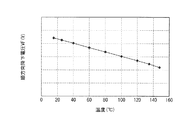
このようなIGBTチップ温度検出部2126によってIGBT2112の温度を測定する場合、定電流源2170からIGBT2112と同一チップ内に埋め込まれた温度検出用ダイオード2142に定電流を供給する。これによって、温度検出用ダイオード2142の両電圧VF(VF電圧信号とも称す)が、図16に示すように温度に比例した電圧値となる。即ち、温度検出用ダイオード2142のチップ温度が165℃ではVF=1.5V、25℃ではVF=2.0Vとして得られ、実際にはVFの変化量500mVが温度信号のフルスパンとなる。
When the temperature of the
図17は、上記のバッファ回路2171と、レベル変換器2177と、三角波発生器2178と、コンパレータ2179とを有して成るVF/PWM変換回路2180の詳細を示す。
三角波発生器2178は、コンパレータ2201及びオペアンプ2202と、これら2201,2202の−,+入力端子と出力端子並びに電源Vcc1及びアースとの間に図示のように接続された抵抗器R21,R22、R23,R24,R25,R26と、コンデンサC11とを備えている。図15と同じ構成については同じ符号を用いて説明する。
FIG. 17 shows details of the VF /
The
三角波発生器2178からは三角波信号が所定の上限値と下限値との間で発生されている。
温度検出用ダイオード2142の順方向降下電圧VFは、バッファ回路2171でインピーダンス変換された後、レベル変換器2177にて、三角波信号の上限値と高温(例:165℃)側VFとが合致、三角波信号の下限値と低温(例:25℃)側VFとが合致するように、増幅及びレベルの加減算が行われる。
A triangular wave signal is generated from a
The forward drop voltage VF of the
つまり、レベル変換器2177は、三角波信号の上限と下限との幅のレベル(振幅)に、VF電圧信号の幅のレベルが一致するようにVF電圧信号の幅を拡大する(ゲインの調整)と共に、この拡大したVF電圧信号のレベルの上下が三角波の上限と下限の位置に一致させる(オフセットの調整)。ゲインとオフセットの調整は次のように行う。
That is, the
図17において、抵抗R11,R12にて電源Vcc1の電圧を分圧してオペアンプ2173の+入力とし、電源Vcc1とオペアンプ2173の−入力との間に接続した抵抗R13によってオフセット量を決定する。また、バッファ回路2171の出力とオペアンプ2173の−入力との間に接続された抵抗R14とオペアンプ2173の−入力と出力との間に接続された抵抗R15とによってオペアンプ2173のゲインを決定する。
In FIG. 17, the voltage of the power supply Vcc1 is divided by resistors R11 and R12 to be the + input of the
このレベル合わせを行った後、後段のコンパレータ2179にてレベル変換器2177の出力電圧Vlevと、三角波発生器の出力電圧Vtriとを比較し、Vlev>Vtriの場合はコンパレータ2179の出力を「L」、Vlev<Vtriの場合は「H」とする。
この動作によって生成されるコンパレータ2179の出力パルスのデューティは、VF電圧信号に比例する。例えばデューティ0%は低温(例:25℃)側VF、100%は高温(例:165℃)側VFとして、次段のフォトカプラ2116,2118によるPWM信号の絶縁伝送回路を介して、上及び下アームのスイッチング部2101,2102から制御部2103の2値化回路2191へPWM信号として伝送される。
After this level adjustment, the output voltage Vlev of the
The duty of the output pulse of the
このPWM信号は、2値化回路2191において、当該PWM信号のデューティが0%ではV1、100%ではV2なる電圧(2値化信号V1/V2)が形成されて出力される。この2値化信号V1/V2をバッファ回路2192でインピーダンス変換した後、LPF回路2193にて平滑化して直流レベルに変換すると、温度検出用ダイオード2141,2142の両端電圧VFに相当する各アームと絶縁された出力電圧(IGBTチップ温度電圧信号)Voutを得る事が出来る。
In the
このようにして得られたIGBTチップ温度に比例した電圧信号Voutは、昇降圧コンバータ1102の上位のシステム(図示せず)に伝達され、そのシステムが常にIGBT2111,2111の温度を検出しながら、例えばIGBTチップ温度が所定の温度T1を超過すると、スイッチング周波数を1/2にし、更に所定の温度T2を超過するとスイッチング(昇降圧動作)を停止する保護機能を働かせる。
The voltage signal Vout proportional to the IGBT chip temperature obtained in this way is transmitted to a higher system (not shown) of the buck-
この保護機能の作動は車両の駆動に影響を与えるので、IGBT2111,2112のチップ温度は正確に測定されなければならず、概ね±5%の精度が要求される。チップ温度の測定の際の誤差要因は大別すると、IGBTチップに埋め込まれた温度検出用ダイオード2141,2142の順方向降下電圧VF値及び温度係数のバラツキと、バッファ回路2171、レベル変換器2177、三角波発生器2178、フォトカプラ(PWM信号の絶縁伝送回路)2116、2値化回路2191、バッファ回路2192及びLPF回路2193から成る回路系のバラツキとの2種類となる。
Since the operation of this protection function affects the driving of the vehicle, the chip temperatures of the
温度検出用ダイオード2141,2142のVF値のバラツキは、半導体プロセスに起因する要因が主で有るので、全体の許容誤差±5%のうち、例えばその6割である±3%をVF値のバラツキとして見込むと、回路系では±2%の誤差に抑制する必要がある。このため各々の回路では±0.5%の誤差に抑えた性能が求められる。
このため、抵抗素子、定電圧素子、オペアンプ等の回路素子は高精度品を用いる必要があるが、車両の環境温度は−40〜+105℃と広範囲での動作保証、車両用としての高信頼性及びクレームを生じた場合の敏速な対応が求められる点から、国内の大手半導体メーカー等の車載対応ICから選択せざるを得ない。
The variations in the VF values of the
For this reason, it is necessary to use highly accurate circuit elements such as resistance elements, constant voltage elements, operational amplifiers, etc., but the environmental temperature of the vehicle is assured to operate in a wide range of −40 to + 105 ° C., and high reliability for vehicles. From the point that prompt response in the case of a complaint is required, it must be selected from in-vehicle ICs such as major domestic semiconductor manufacturers.
図17に示すVF/PWM変換回路2180において、定電流源2170(図17には不図示、図15参照)から供給される定電流IFにより、温度検出用ダイオード2142に生ずる温度に比例した順方向降下電圧(チップ温度が165℃ではVF=1.5V、25℃ではVF=2.0V)がバッファ回路2171でインピーダンス変換され、レベル変換器2177に供給される。
レベル変換器2177のオペアンプ2173の+入力端子には、電源Vcc1の電位を抵抗器R11とR12で分圧した電位Vcc11に固定されているので、オペアンプ2173の出力電圧は下式(1)で表される。
In the VF /
Since the potential of the power supply Vcc1 is fixed to the potential Vcc11 obtained by dividing the potential of the power supply Vcc1 by the resistors R11 and R12 at the + input terminal of the

一方、三角波発生器2178からの三角波信号の上限値Vsuと下限値Vsdは下式(2)及び(3)で表される。なお、コンパレータ2201の−入力端子には電源Vcc1を抵抗器R21とR22で分圧された電位Vcc12に固定されている。
On the other hand, the upper limit value Vsu and the lower limit value Vsd of the triangular wave signal from the
但し、Vic3LOWは、コンパレータ2201の「L」レベル出力である。また、「//」はその前後に示す抵抗等を並列接続した際の合成値を簡易表記したものであり、例えば(3)式の「R24//R25」はR24とR25とを並列接続した時の合成抵抗値を示す。以下においても同様である。
このような三角波発生器2178の出力信号の上限値Vsuと下限値Vsdの三角波と、レベル変換器2177の出力とを、コンパレータ2179で比較して、下式(4)〜(6)で表される温度に比例したパルス幅のPWM信号を生成する。
However, V ic3LOW is an “L” level output of the
The triangular wave of the upper limit value Vsu and the lower limit value Vsd of the output signal of the
このPWM信号は、図18に詳細構成を示すPWM・アナログ変換器2190のフォトカプラ2116で絶縁された後、2値化回路2191、バッファ回路2192、LPF回路2193へ伝送される。このPWM信号のデューティ(Duty)とLPF回路2193の出力(IGBTチップ温度電圧信号Vout)との関係は下式(7)で表される。
This PWM signal is insulated by a
但し、Vceは、Tr2250の飽和状態におけるコレクタ・エミッター間の電圧であり、概ね0.15Vである。また、VLPFは、LPF回路2193の出力である。
これらの式(1)〜(7)において、±0.1%の高精度抵抗器を用いれば、LPF回路2193の出力の誤差は電源Vcc1,Vcc2のバラツキに依存することになる。
特に、Vcc1はフルスパンが500mVの信号を取り扱う回路に用いられるので高安定、高精度な電圧源が必要とされ、高精度なシャントレギュレータを用いる必要がある。
また、Vcc2はフルスパンが4Vの信号を取り扱うので、Vcc1よりも高い精度は要求されない。
However, V ce is the voltage between the collector and emitter of the saturation Tr2250, is generally 0.15V. V LPF is an output of the
In these equations (1) to (7), if a high-precision resistor of ± 0.1% is used, the error in the output of the
In particular, since Vcc1 is used in a circuit that handles a signal having a full span of 500 mV, a highly stable and highly accurate voltage source is required, and a highly accurate shunt regulator must be used.
Further, since Vcc2 handles a signal having a full span of 4V, higher accuracy than Vcc1 is not required.
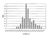
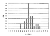
図19に電源Vcc1にシャントレギュレータを用いた場合の電位Vcc1のバラツキ分布を、図20に電源Vcc2に標準レギュレータを用いた場合の電位Vcc2のバラツキ分布を示す。
これらの基準電圧源の電圧バラツキは上式(1)〜(7)において、Vcc1,Vcc2の値が変わるので、温度に比例したLPF回路2193の出力において、温度幅が130℃で出力電圧幅が4Vに割り当てているスパン、及び温度25℃で出力が4.5Vに割り当てているオフセットが影響を受ける事になる。
FIG. 19 shows the variation distribution of the potential Vcc1 when the shunt regulator is used for the power supply Vcc1, and FIG. 20 shows the variation distribution of the potential Vcc2 when the standard regulator is used for the power supply Vcc2.
In the voltage variation of these reference voltage source is above formula (1) ~ (7), V cc1, the value of V cc2 is changed, the output of the
上記のVcc1を変動させた場合のLPF回路2193の出力への影響を図21及び図22に、Vcc2を変動させた場合のLPF回路2193の出力への影響を図23及び図24に示す。
Vcc1,Vcc2の出力電圧のバラツキの分布が正規分布と仮定した場合、分布の中心値から3σまでの範囲において、IGBTチップ温度電圧信号(LPF出力)Voutに生じる誤差及び区間内累積分布割合を統計計算した。この結果、1.2σ以下(母集団の77%)では、回路による温度計測は、最大±2.88%以下に抑制出来るが、残りの23%は±2.88%を超過してしまうので、図17に示したレベル変換器2177における抵抗器R13をオフセット調整用、R15をゲイン調整用として抵抗値を変更しなければならない。
The effect on the output of the
If V cc1, variations in the distribution of the output voltage of the V cc2 is assumed normal distribution, in the range from the center value of the distribution to the 3 [sigma], IGBT chip temperature voltage signal (LPF output) error and interval in cumulative distribution ratio caused Vout Was statistically calculated. As a result, at 1.2σ or less (77% of the population), the temperature measurement by the circuit can be suppressed to a maximum of ± 2.88% or less, but the remaining 23% exceeds ± 2.88%. In the
このため、抵抗器R13,R15に関しては、±5σ以内であれば調整出来るように、予め抵抗値の低い素子を実装しておき、これをレーザートリミング装置で抵抗パターンを部分的に切断することによって目標とする調整値に合致させる必要がある。
この場合には、チップ温度測定回路の入力信号として既知の電圧(2点:VF1,VF2)を入力し、その時の出力電圧(2点:Vout1_m,Vout2_m)を測定し、目標電圧値(2点:Vout1_s,Vout2_s)からのずれを算出する。そして、算出したずれに基づいて抵抗R13及びR15の目標抵抗値を決定し、各抵抗R13及びR15のトリミングを実施する。
For this reason, with regard to the resistors R13 and R15, an element having a low resistance value is mounted in advance so that it can be adjusted within ± 5σ, and this is performed by partially cutting the resistance pattern with a laser trimming device. It is necessary to match the target adjustment value.
In this case, a known voltage (2 points: VF1, VF2) is input as an input signal of the chip temperature measuring circuit, the output voltage (2 points: Vout1_m, Vout2_m) at that time is measured, and the target voltage value (2 points) : Vout1_s, Vout2_s) is calculated. Then, based on the calculated deviation, target resistance values of the resistors R13 and R15 are determined, and trimming of the resistors R13 and R15 is performed.
その後に、トリミング後のチップ温度測定回路に対して、再度、既知の電圧(2点:VF1,VF2)を入力し、その時の出力電圧2点:Vout1_m,Vout2_m)を測定し、目標電圧値(2点:Vout1_s,Vout2_s)に対して、許容誤差の範囲内であることを確認している。
このような、調整方法では、高価なレーザートリミング装置を導入する必要があるとともに、抵抗調整工数がかかり、製造コスト高の要因となるという未解決の課題がある。さらに、再調整ができないため、ある程度の不良率を考慮しなければならないという未解決の課題もある。
After that, a known voltage (2 points: VF1, VF2) is input again to the chip temperature measurement circuit after trimming, and the output voltage at that time: 2 points: Vout1_m, Vout2_m) is measured, and the target voltage value ( 2 points: Vout1_s, Vout2_s), it is confirmed that they are within the allowable error range.
Such an adjustment method has an unresolved problem that it is necessary to introduce an expensive laser trimming apparatus, and it takes a man-hour for resistance adjustment, which causes a high manufacturing cost. Furthermore, since readjustment cannot be performed, there is an unsolved problem that a certain defect rate must be considered.
このため、チップ温度測定回路の温度補正を電子的に行うことが考えられている。
たとえば、特許文献1及び特許文献2に記載の従来例では、外部ツールを介して転送書込みされる制御プログラムと制御定数とを格納した不揮発メモリと、演算処理用RAMメモリとを有するマイクロプロセッサを備えた車載エンジン制御装置が開示されている。この車載エンジン制御装置は、定電圧電源回路部と、温度センサと多チャンネルAD変換器とを備える。
For this reason, it is considered to electronically correct the temperature of the chip temperature measuring circuit.
For example, the conventional examples described in
さらに、上記不揮発メモリは、校正処理データと換算処理データとを格納している。ここで、校正処理データは、車載エンジン制御装置の調整操作段階において、外部設置された計測装置による測定結果を外部ツールから転送書込したデータである。この校正処理データは、調整操作時点における環境温度から推定される定電圧電源回路部の近傍温度と、調整操作時点における定電圧電源回路部の実際の出力電圧とに関する外部計測データとを含んでいる。 Further, the nonvolatile memory stores calibration processing data and conversion processing data. Here, the calibration processing data is data obtained by transferring and writing a measurement result from an externally installed measuring device from an external tool in the adjustment operation stage of the in-vehicle engine control device. This calibration processing data includes external measurement data relating to the temperature near the constant voltage power supply circuit unit estimated from the environmental temperature at the time of adjustment operation and the actual output voltage of the constant voltage power supply circuit unit at the time of adjustment operation. .
換算処理データは、定電圧電源回路部の近傍温度対出力電圧の変動特性に関して予め多数の製品について実測測定して統計的に算出された平均的な電圧変動特性データを含んでいる。
そして、温度検出センサの検出出力と校正処理データと換算処理データとを参照することによって、異なる温度環境下における定電圧電源回路部の出力電圧を推定し、推定した出力電圧を定電圧で除した値でなる補正係数をアナログ入力電圧に対するデジタル変換値掛け合わせて、補正されたデジタル変換値を得るようにしている。
The conversion processing data includes average voltage fluctuation characteristic data that is statistically calculated by actually measuring and measuring a large number of products in advance with respect to fluctuation characteristics of the temperature near the constant voltage power supply circuit section versus the output voltage.
Then, by referring to the detection output of the temperature detection sensor, the calibration processing data, and the conversion processing data, the output voltage of the constant voltage power supply circuit unit under different temperature environments is estimated, and the estimated output voltage is divided by the constant voltage. The corrected digital conversion value is obtained by multiplying the correction coefficient consisting of the value by the digital conversion value for the analog input voltage.
また、特許文献3に記載された従来例では、スイッチング素子の温度検出用のダイオードの出力値を、モータを組み付けた際の、モータ温度検出値とスイッチング温度検出値に基づくキャリブレーション値(温度補正値)によって補正するようにしている。ここで、温度検出用ダイオードの温度特性及び上記キャリブレーション値(温度補正値)はメモリ等の記憶媒体に記憶されている。
Further, in the conventional example described in
さらに、特許文献4に記載された従来例では、半導体スイッチング素子の動作温度を検出する温度検知手段と、この温度検出手段からの検知信号が不揮発メモリに記憶された規定のトリップレベルを上回ったとき、上記半導体スイッチング素子の動作を停止させる過温度保護手段と、前記トリップレベルの補正を行う特性補正手段とを備えた半導体装置が記載されている。
Furthermore, in the conventional example described in
さらに、特許文献5に記載された従来例では、半導体素子に温度測定用ダイオードを形成し、この温度測定用ダイオードの順方向電圧降下の温度特性から温度測定用ダイオードが設けられている位置の温度データを求めるようにしている。一方、電流センス用エミッタから流れるセンス電流を電流検出回路で測定し、演算部でセンス電流の値に基づいて、補正温度を算出する。そして、演算部は、温度データに補正温度を加算することにより、接合部温度を求めるようにしている。そして、メモリには、電流検出回路で検出した電流値に対応する補正温度がテーブル形式で格納されており、電流検出回路で検出した電流値を受信するとテーブルを参照して補正温度を算出するようにしている。
Furthermore, in the conventional example described in
ところで、特許文献1及び2に記載の従来例にあっては、不揮発性メモリに記憶されている標準特性における温度−出力電圧特性を換算処理データとして記憶するとともに、車載エンジン制御装置の調整操作段階における校正温度と、この校正温度における出力電圧を校正処理データとして記憶して置く。そして、実用温度を測定したときに、不揮発性メモリに記憶された校正処理データ及び換算処理データを参照して、実用計測温度における定電圧出力を所定の演算式に従って算出する。算出した定電圧出力を基準電圧で除して補正係数を演算し、この補正係数をデジタル変換値に掛け合わせて補正されたデジタル変換値を得るようにしている。
By the way, in the conventional examples described in
このため、不揮発性メモリに校正処理データ及び換算処理データを格納する必要があり、記憶容量が多くなるとともに、実用温度が変化する毎に、校正処理データと換算処理データを参照した演算処理を繰り返す必要があり、演算処理負荷が大きくなるという未解決の課題がある。 For this reason, it is necessary to store the calibration processing data and the conversion processing data in the nonvolatile memory, the storage capacity increases, and the calculation processing referring to the calibration processing data and the conversion processing data is repeated every time the practical temperature changes. There is an unsolved problem that the calculation processing load becomes large.
同様に、特許文献3に記載の従来例にあっては、モータ駆動装置の組み付け時に、モータ温度算出部で算出したモータ温度とスイッチング素子温度算出部で算出したスイッチング素子の温度との差分をスイッチング素子温度算出部において算出結果を補正するキャリブレーション値(温度補正値)としてメモリ等の記憶媒体に記憶している。そして、このキャリブレーション値でスイッチング素子温度検出用のダイオードの出力値の補正を行うことにより、オフセット補正を行うようにしている。しかしながら、特許文献3に記載の従来例にあっては、単にキャリブレーション値をスイッチング素子温度検出用のダイオードの出力に加算するだけであり、温度−出力電圧特性の傾きが異なる場合には適用することができないという未解決の課題がある。
Similarly, in the conventional example described in
また、特許文献4に記載の従来例にあっては、過温度の判断基準となるトリップレベルの補正を、EPROMに書込まれた特性補正信号に基づいて接続するコンデンサ数を選択することにより行うようにしているので、温度−出力電圧特性の傾きが異なる場合には適用することができないという未解決の課題がある。
Further, in the conventional example described in
同様に、特許文献5に記載の従来例にあっては、半導体素子の電流センス用エミッタから流れるセンス電流の値に基づいてメモリに格納された電流値対補正温度のテーブルを参照して補正温度を算出し、この補正温度を温度検出回路から取得した温度データに加算して接合部温度を算出するようにしており、温度−出力電圧特性の傾きが異なる場合には適用することができないという未解決の課題がある。
そこで、本発明は、上記従来例の未解決の課題に着目してなされたものであり、設計上の特性と実測した特性との傾きが異なる場合に、容易に且つ正確に温度検出ができるパワー半導体装置の温度測定装置を提供することを目的としている。
Similarly, in the conventional example described in
Therefore, the present invention has been made paying attention to the unsolved problems of the above-described conventional example, and can easily and accurately detect the temperature when the slope between the designed characteristic and the actually measured characteristic is different. An object of the present invention is to provide a temperature measuring device for a semiconductor device.
上記目的を達成するために、本発明に係るパワー半導体装置の温度測定装置の第1の態様は、シリコンチップにパワースイッチング素子と温度検出用ダイオードとを設けたパワー半導体装置における前記パワースイッチング素子のチップ温度を検出するチップ温度検出回路を備えたパワー半導体装置の温度測定装置である。そして、前記チップ温度検出回路は、前記温度検出用ダイオードに定電流を供給する定電流源と、前記温度検出用ダイオードの両端の順方向電圧をデジタル変換して測定値として出力するA/D変換器と、該A/D変換器から出力される測定値が入力され、当該測定値に基づいて前記チップ温度を演算する演算処理部とを少なくとも備えている。ここで、前記演算処理部は、校正処理部とチップ温度演算部とを備えている。校正処理部は、前記チップ温度検出回路の誤差の校正時に、前記温度検出用ダイオードに代えて既知の異なる複数の基準電圧値を印加する基準電圧源を接続し、前記複数の基準電圧値をそれぞれ印加したときの前記A/D変換器から出力される測定値を結ぶ線分の傾きを演算し、演算した線分の傾きと、前記A/D変換器から出力される測定値のうちの1つであるオフセット補正値とを記憶部に記憶する。チップ温度演算部は、前記温度検出用ダイオードによる温度測定時に、前記A/D変換器から出力される測定値と、前記記憶部に記憶されている線分の傾き及びオフセット補正値とに基づいて補正測定値を演算し、当該補正測定値に基づいて前記チップ温度を演算する。前記校正処理部は、前記基準電圧を印加した時の前記A/D変換器から得られる測定値の測定を複数回行い、複数回の測定値の平均値を測定値としている。 In order to achieve the above object, a first aspect of a power semiconductor device temperature measuring device according to the present invention is a power semiconductor device in which a power switching element and a temperature detection diode are provided on a silicon chip. A temperature measurement device for a power semiconductor device including a chip temperature detection circuit for detecting a chip temperature. The chip temperature detection circuit converts the forward voltage across the temperature detection diode to a constant current source that supplies a constant current to the temperature detection diode and outputs it as a measurement value by digital conversion And a calculation processing unit that receives the measurement value output from the A / D converter and calculates the chip temperature based on the measurement value. Here, the calculation processing unit includes a calibration processing unit and a chip temperature calculation unit. The calibration processing unit connects a reference voltage source that applies a plurality of known different reference voltage values in place of the temperature detection diode at the time of calibration of the error of the chip temperature detection circuit, and each of the plurality of reference voltage values The slope of the line segment connecting the measurement values output from the A / D converter when applied is calculated, and the calculated slope of the line segment and one of the measurement values output from the A / D converter are calculated. Is stored in the storage unit. The chip temperature calculation unit is based on the measurement value output from the A / D converter and the slope and offset correction value stored in the storage unit during temperature measurement by the temperature detection diode. A corrected measurement value is calculated, and the chip temperature is calculated based on the corrected measurement value. The calibration processing unit performs measurement of a measurement value obtained from the A / D converter when the reference voltage is applied a plurality of times, and uses an average value of the plurality of measurement values as a measurement value .
また、本発明に係るパワー半導体装置の温度測定装置の第2の態様は、シリコンチップにパワースイッチング素子と温度検出用ダイオードとを設けたパワー半導体装置における前記パワースイッチング素子のチップ温度を検出するチップ温度検出回路を備えたパワー半導体装置の温度測定装置である。前記チップ温度検出回路は、前記温度検出用ダイオードに定電流を供給する定電流源と、前記温度検出用ダイオードの両端の順方向電圧を入力信号としてパルス幅変調信号を出力するパルス幅変調回路と、該パルス幅変調回路から出力されるパルス幅変調信号を電気的に絶縁して伝送させる絶縁伝送回路と、該絶縁伝送回路の出力信号を平滑化するローパスフィルタと、該ローパスフィルタのフィルタ出力をデジタル変換して測定値として出力するA/D変換器と、該A/D変換器から出力される測定値が入力され、当該測定値に基づいて前記チップ温度を演算する演算処理部とを少なくとも備えている。ここで、前記演算処理部は、校正処理部とチップ温度演算部とを備えている。校正処理部は、前記チップ温度検出回路の誤差の校正時に、前記温度検出用ダイオードに代えて既知の異なる複数の基準電圧値を印加する基準電圧源を接続し、前記複数の基準電圧値をそれぞれ印加したときの前記A/D変換器から出力される測定値を結ぶ線分の傾きを演算し、演算した線分の傾きと、前記A/D変換器から出力される測定値のうちの1つであるオフセット補正値とを記憶部に記憶する。チップ温度演算部は、前記温度検出用ダイオードによる温度測定時に、前記A/D変換器から出力される測定値と、前記記憶部に記憶されている線分の傾き及びオフセット補正値とに基づいて補正測定値を演算し、当該補正測定値に基づいて前記チップ温度を演算する。前記校正処理部は、基準電圧を印加した時の前記A/D変換器から出力される測定値に対して、前記パルス幅変調回路に含まれる三角波発生回路の発振周期の整数倍の期間においてサンプリングを行い、サンプリング値の平均値を測定値としている。 According to a second aspect of the temperature measuring device for a power semiconductor device according to the present invention, a chip for detecting a chip temperature of the power switching element in a power semiconductor device in which a power switching element and a temperature detecting diode are provided on a silicon chip. 1 is a temperature measurement device for a power semiconductor device including a temperature detection circuit. The chip temperature detection circuit includes a constant current source that supplies a constant current to the temperature detection diode, a pulse width modulation circuit that outputs a pulse width modulation signal using a forward voltage across the temperature detection diode as an input signal, and An insulation transmission circuit for electrically insulating and transmitting the pulse width modulation signal output from the pulse width modulation circuit, a low-pass filter for smoothing the output signal of the insulation transmission circuit, and a filter output of the low-pass filter. At least an A / D converter that performs digital conversion and outputs a measurement value, and an arithmetic processing unit that receives the measurement value output from the A / D converter and calculates the chip temperature based on the measurement value I have. Here, the calculation processing unit includes a calibration processing unit and a chip temperature calculation unit. The calibration processing unit connects a reference voltage source that applies a plurality of known different reference voltage values in place of the temperature detection diode at the time of calibration of the error of the chip temperature detection circuit, and each of the plurality of reference voltage values The slope of the line segment connecting the measurement values output from the A / D converter when applied is calculated, and the calculated slope of the line segment and one of the measurement values output from the A / D converter are calculated. Is stored in the storage unit. The chip temperature calculation unit is based on the measurement value output from the A / D converter and the slope and offset correction value stored in the storage unit during temperature measurement by the temperature detection diode. A corrected measurement value is calculated, and the chip temperature is calculated based on the corrected measurement value. The calibration processing unit samples the measurement value output from the A / D converter when a reference voltage is applied in a period that is an integral multiple of the oscillation period of the triangular wave generation circuit included in the pulse width modulation circuit. The average value of the sampling values is used as the measurement value.
また、本発明に係るパワー半導体装置の温度測定装置の第3の態様は、前記記憶部が、前記演算処理部内に形成した不揮発性メモリ領域で形成されている。 According to a third aspect of the temperature measuring device for a power semiconductor device according to the present invention, the storage unit is formed of a nonvolatile memory region formed in the arithmetic processing unit.
また、本発明に係るパワー半導体装置の温度測定装置の第4の態様は、前記校正処理部が、既知の異なる複数の基準電圧値を、チップ温度の測定範囲の最大及び最小温度における前記温度検出ダイオードの順方向電圧値の範囲内に設定している。
また、本発明に係るパワー半導体装置の温度測定装置の第5の態様は、前記校正処理部が、既知の異なる複数の基準電圧値の両端の2点が、チップ温度の測定範囲の最大及び最小温度における前記温度検出ダイオードの順方向電圧値と同等の値又は近傍の値に設定されている。
According to a fourth aspect of the temperature measurement device for a power semiconductor device according to the present invention, the calibration processing unit detects the plurality of known different reference voltage values at the maximum and minimum temperatures of the chip temperature measurement range. It is set within the range of the forward voltage value of the diode.
Further, according to a fifth aspect of the temperature measuring device for a power semiconductor device according to the present invention, the calibration processing unit is configured such that two points at both ends of a plurality of different known reference voltage values are the maximum and minimum of the chip temperature measurement range. The temperature is set to a value equal to or close to the forward voltage value of the temperature detection diode.
本発明によれば、校正時に、温度検出用ダイオードに代えて基準電圧源を接続し、この基準電圧源で既知の複数の基準電圧を印加し、そのときの基準電圧毎のA/D変換器の測定値を結ぶ線分の傾きを演算し、この線分の傾きとA/D変換器の測定値の1つであるオフセット補正値とを記憶部に記憶する。そして、温度検出用ダイオードによる温度測定時に、A/D変換器から出力される測定値に対して、記憶部に記憶されている線分の傾き及びオフセット補正値に基づいて補正演算を行う。このため、校正処理部で、既知の複数の基準電圧を使用することにより、チップ温度検出回路の特性に基づく線分の傾きを容易に算出することができる。そして、測定補正演算部では、記憶されている線分の傾き及びオフセット補正値と、A/D変換器から出力される測定値とに基づいて簡易な演算処理で補正された測定値を算出することができ、演算処理部での演算負荷を減少させることができる。 According to the present invention, at the time of calibration, a reference voltage source is connected instead of the temperature detection diode, a plurality of known reference voltages are applied by this reference voltage source, and an A / D converter for each reference voltage at that time The slope of the line segment connecting the measured values is calculated, and the slope of this line segment and the offset correction value that is one of the measured values of the A / D converter are stored in the storage unit. Then, at the time of temperature measurement by the temperature detection diode, correction calculation is performed on the measurement value output from the A / D converter based on the slope of the line segment and the offset correction value stored in the storage unit. For this reason, the inclination of the line segment based on the characteristics of the chip temperature detection circuit can be easily calculated by using a plurality of known reference voltages in the calibration processing unit. Then, the measurement correction calculation unit calculates a measurement value corrected by a simple calculation process based on the stored line segment inclination and offset correction value and the measurement value output from the A / D converter. It is possible to reduce the calculation load in the calculation processing unit.
以下、本発明に係るパワー半導体装置の温度測定装置の第1の実施形態について図面を参照しながら説明する。
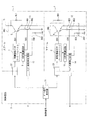
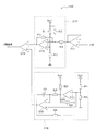
図1は、本発明が適用されるインテリジェントパワーモジュール(IPM:Inteligent Power Module)の概略構成を示すブロック図である。
図1において、インテリジェントパワーモジュールは、負荷へ流入する電流を制御する上アーム1および下アーム2を備えている。これら上アーム1および下アーム2は、負荷へ流入する電流を通電および遮断するパワースイッチング素子SWU、SWDを有する。これらパワースイッチング素子SWU、SWDの導通および非導通を指示する制御信号がそれぞれ制御回路3で生成される。ここで、制御回路3は、CPUまたは論理IC、あるいは論理ICとCPUが搭載されたシステムLSIなどで構成することができる。
Hereinafter, a first embodiment of a temperature measuring device for a power semiconductor device according to the present invention will be described with reference to the drawings.
FIG. 1 is a block diagram showing a schematic configuration of an intelligent power module (IPM: Intelligent Power Module) to which the present invention is applied.
In FIG. 1, the intelligent power module includes an
また、上アーム1、下アーム2のパワースイッチング素子SWU、SWDは直列に接続されている。上アーム1、下アーム2のパワースイッチング素子SWU、SWDの直列接続点を外部に導出する端子の図示は省略する。このようなインテリジェントパワーモジュールを、図12に示すように、パワースイッチング素子SWU、SWDの直列接続点にリアクトルを接続すれば、昇降圧コンバータを構成することができる。あるいは、このようなインテリジェントパワーモジュールを3組用い、パワースイッチング素子SWU、SWDの直列接続回路の両端に直流電源を接続し、パワースイッチング素子SWU、SWDの直列接続点を交流出力端子とすることで3相インバータを構成することができる。
The power switching elements SWU and SWD of the
また、図1は、上アーム1、下アーム2のパワースイッチング素子SWU、SWDの直列回路の1組をパッケージしたいわゆる2in1構成のインテリジェントパワーモジュールであるが、上アーム1、下アーム2のパワースイッチング素子SWU、SWDの直列回路の3組をパッケージしたいわゆる6in1構成のインテリジェントパワーモジュールとして構成することもできる。
FIG. 1 shows an intelligent power module having a so-called 2-in-1 configuration in which a set of series circuits of the power switching elements SWU and SWD of the
そして、パワースイッチング素子SWUには、ゲート信号SU4に基づいてスイッチング動作を行うIGBT5が設けられ、IGBT5に流れる電流と逆方向に電流を流すフリーホイーリングダイオードDU1がIGBT5に並列に接続されている。また、IGBT5が形成されたシリコンチップには、チップの温度変化に対応する順方向電圧が得られる温度検出用ダイオードDU2が設けられているとともに、エミッタ電流を分流してエミッタ電流値を検出するためにIGBT5に設けられた第2のエミッタ端子に接続された抵抗RU1、RU2により過電流を検出する過電流検出部11が設けられている。
The power switching element SWU is provided with an
また、パワースイッチング素子SWDには、ゲート信号SD4に従ってスイッチング動作を行うIGBT6が設けられ、IGBT6に流れる電流と逆方向に電流を流すフリーホイーリングダイオードDD1がIGBT6に並列に接続されている。また、IGBT6が形成されたシリコンチップには、チップの温度変化に対応する順方向電圧が得られる温度検出用ダイオードDD2が設けられているとともに、エミッタ電流を分流してエミッタ電流値を検出するためにIGBT6に設けられた第2のエミッタ端子に接続された抵抗RD1、RD2により過電流を検出する過電流検出部12が設けられている。
Further, the power switching element SWD is provided with an
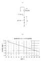
温度検出用ダイオードDU2およびDD2は、図2に示すように、ダイオード1個では温度変化による順方向電圧がおおよそ0.5V〜0.7Vと低くて取り扱いにくいため、3個のダイオードを直列接続する構成を採用して温度変化による順方向電圧をチップ温度200℃で1.38V、−50℃で2.43Vとなるように設定してある。 As shown in FIG. 2, the temperature detecting diodes DU2 and DD2 have three diodes connected in series because a single diode has a low forward voltage of about 0.5V to 0.7V due to a temperature change and is difficult to handle. By adopting the configuration, the forward voltage due to temperature change is set to 1.38 V at a chip temperature of 200 ° C. and 2.43 V at −50 ° C.
そして、上アーム1側には、IGBT5の制御端子を駆動するためのゲート信号SU4を生成するゲートドライバIC7が設けられている。また、上アーム1側には、内蔵する定電流源から温度検出用ダイオードDU2に例えば200μAの定電流を供給し、このときの温度検出用ダイオードDU2の順方向電圧VFでなる過熱検知信号SU6を監視するチップ温度検出回路13が設けられている。さらに、上アーム1側には、過電流検出部11からの過電流検知信号SU5を監視してIGBT保護信号を生成し、IGBT保護信号をゲートドライバIC7に供給するIGBT保護回路9が設けられている。
On the
また、下アーム2側には、IGBT6の制御端子を駆動するためのゲート信号SD4を生成するゲートドライバIC8が設けられている。また、下アーム2側には、内蔵する定電流源から温度検出用ダイオードDD2に例えば200μAの定電流を供給し、このときの温度検出用ダイオードDD2の順方向電圧VFでなる過熱検知信号SD6を監視するチップ温度検出回路14が設けられている。さらに、下アーム2側には、過電流検出部12からの過電流検知信号SD5を監視してIGBT保護信号を生成し、IGBT保護信号をゲートドライバIC8に供給する温度測定部を含むIGBT保護回路10が設けられている。
On the
そして、IGBT保護回路9および10は、過電流検知信号SD5,SU5の電流値が予め設定した所定電流値Iovを超えた場合に、ゲート信号の出力を停止するIGBT保護信号をゲートドライバIC7および8に出力する。
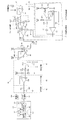
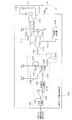
チップ温度検出回路13および14は、共に同じ回路構成を有し、両者を代表してチップ温度検出回路13の構成を説明すると、図3に示すように構成されている。すなわち、定電流源70から定電流IFを温度検出用ダイオードDU2に供給したときの温度検出用ダイオードDU2の順方向電圧VFを、バッファアンプIC1でインピーダンス変換した後、レベル変換器77に供給し、レベル変換器77からレベル調整された電圧Vlevを出力する。
Then, the
The chip
このレベル変換器77は、オペアンプIC2を有し、このオペアンプIC2の反転入力端子にバッファアンプIC1の出力が抵抗R14を介して入力されている。また、オペアンプIC2の非反転入力端子には、直流電源Vcc1を抵抗R11およびR12で分圧した電位Vcc11が入力されている。さらに、直流電源Vcc1が抵抗R13を介してオペアンプIC2の反転入力端子および抵抗R14との間に供給され、オペアンプIC2の反転入力端子と出力端子との間に抵抗R15が接続されている。
このレベル変換器77の出力電圧Vlevは、下記(8)式で表わされる。
The level converter 77 has an operational amplifier IC2, and the output of the buffer amplifier IC1 is input to the inverting input terminal of the operational amplifier IC2 through a resistor R14. The potential Vcc11 obtained by dividing the DC power supply Vcc1 by the resistors R11 and R12 is input to the non-inverting input terminal of the operational amplifier IC2. Further, the DC power source Vcc1 is supplied between the inverting input terminal of the operational amplifier IC2 and the resistor R14 via the resistor R13, and the resistor R15 is connected between the inverting input terminal and the output terminal of the operational amplifier IC2.
The output voltage Vlev of the level converter 77 is expressed by the following equation (8).
なお、このレベル変換は線形変換である。
また、チップ温度検出回路13は、パルス幅変調回路76を備えている。このパルス幅変調回路76は、三角波信号Vtriを発生する三角波発生回路78とコンパレータIC5とを備えている。
This level conversion is a linear conversion.
The chip
三角波発生回路78は、コンパレータIC3とこのコンパレータIC3の出力が入力される積分器を構成するオペアンプIC4とを備えている。コンパレータIC3の反転入力側には、直流電源Vcc1を抵抗R21およびR22で分圧した電位Vcc12が入力され、非反転入力側にはオペアンプIC4の出力端子が抵抗R26を介して接続され、さらに、コンパレータIC3の非反転入力端子および出力端子間に抵抗R25が接続されている。
The triangular
また、コンパレータIC3の出力端子には、直流電源Vcc1が抵抗R23を介して接続され、さらにコンパレータIC3の出力端子が抵抗R24を介してオペアンプIC4の反転入力端子に接続されている。
オペアンプIC4の反転入力端子および出力端子間には積分用コンデンサC11が接続されている。
Further, the DC power supply Vcc1 is connected to the output terminal of the comparator IC3 via the resistor R23, and the output terminal of the comparator IC3 is connected to the inverting input terminal of the operational amplifier IC4 via the resistor R24.
An integrating capacitor C11 is connected between the inverting input terminal and the output terminal of the operational amplifier IC4.
そして、レベル変換器77でレベル調整された出力電圧Vlevおよび三角波発生回路78から出力される三角波信号VtriがコンパレータIC5に入力されている。このコンパレータIC5は、出力電圧Vlevおよび三角波信号Vtriを比較して、Vlev<Vtriであるときには高レベルとなり、Vlev≧Vtriであるときに低レベルとなるPWM信号を出力する。
このコンパレータIC5から出力されるPWM信号は、次段のフォトカプラ90によるPWM信号の絶縁伝送回路を介して上アーム1および下アーム2から、制御回路3側に設けられているPWM−アナログ変換回路91に温度検出用のPWM信号として伝送される。
The output voltage Vlev adjusted in level by the level converter 77 and the triangular wave signal Vtri output from the triangular
The PWM signal output from the comparator IC5 is supplied from the
このPWM−アナログ変換回路91では、フォトカプラ90から入力されるPWM信号を2値信号に変換する2値化回路92に供給し、この2値化回路92でデューティ比が0%では電圧V1、デューティ比が100%では電圧V2となる2値信号を生成する。この2値信号をバッファ回路93でインピーダンス変換した後に、ローパスフィルタ回路94で平滑化して直流レベルに変換することにより、IGBTチップ温度に比例したIGBTチップ温度信号Voutを得ることができる。
In this PWM-
このIGBTチップ温度信号Voutが定電圧素子100から定電圧が供給されたA/D変換器101に入力され、このA/D変換器101でデジタル変換してデジタル値の測定値Vout_mとして出力される。
そして、A/D変換器101から出力される測定値が演算処理部としてのマイクロコンピュータ102に入力される。
The IGBT chip temperature signal Vout is input to the A /
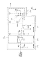
Then, the measurement value output from the A /
このマイクロコンピュータ102は、A/D変換器101に接続されたインタフェース回路103と、このインタフェース回路103から入力される測定値を演算処理する中央処理装置(CPU)104とを備えている。また、マイクロコンピュータ102は、中央処理装置104で実行するプログラグラムや実行結果等を記憶するROM及びRAMで構成される揮発性メモリ部105と、後述する校正処理部で算出した線分の傾き及びオフセット補正値を記憶する不揮発性メモリ部106とを備えている。
The
そして、マイクロコンピュータ102の中央処理装置104は、機能ブロック図で表すと、図4に示すように、少なくとも校正処理部107とチップ温度演算部108とを備えている。
校正処理部107では、調整操作段階で、図5に示すように、チップ温度検出回路14の温度測定用ダイオードDU2のアノード及びカソードの接続端子間に電圧印加指令に基づいて印加電圧を変更可能な定電圧源110を接続した状態で校正処理を行う。
The
The
この校正処理は、先ず、定電圧源110で、既知の異なる2つ基準電圧値を印加する。ここで、2つの基準電圧値としては、たとえばチップ温度155℃に相当する電圧値VF1=105298Vと、25℃に相当する電圧値VF2=2.0619Vとを設定する。
そして、各電圧値VF1及びVF2の印加時におけるA/D変換器101から出力される測定値Vout1_m及びVout2_mを読込んで、両測定値Vout1_m及びVout2_mを結ぶ線分の傾きαを演算する。演算した線分の傾きαと、両測定値Vout1_m及びVout2_mの一方であるオフセット補正値Vout1_mとを不揮発性メモリ部106に記憶する。
In this calibration process, first, two different known reference voltage values are applied by the constant voltage source 110. Here, as the two reference voltage values, for example, a voltage value VF1 = 105298V corresponding to the chip temperature 155 ° C. and a voltage value VF2 = 2.0619V corresponding to 25 ° C. are set.
Then, the measurement values Vout1_m and Vout2_m output from the A /
また、チップ温度演算部108では、実際に温度検出用ダイオードDU2を接続した状態で、A/D変換器101から出力される測定値Vout_mを読込み、この測定値Vout_mと不揮発性メモリ部106に記憶されている線分の傾きα及びオフセット補正値Vout1_mとに基づいて後述する演算を行って温度検出用ダイオードDU2の順方向電圧VFを算出する。そして、チップ温度演算部108では、算出した順方向電圧VFをもとに、図2(b)に示す温度検出用ダイオードDU2の温度と順方向電圧の関係を表す特性線図を参照してチップ温度Tcを算出する。
The chip
このとき、A/D変換値は、本来はHexコードで表示しなければならないが、汎用性を持たせるため及び説明を分かりやすくするために、0〜5Vの電圧値で表現する。そして、PWM−アナログ変換回路91の出力は、入力であるパルス幅変調回路76のパルス幅変調信号のオンデューティ:0〜100%に対して、設計値として概ね4.5〜0.5Vとなるように設定されている。
At this time, the A / D conversion value must originally be displayed in Hex code, but is expressed by a voltage value of 0 to 5 V in order to provide versatility and make the explanation easy to understand. The output of the PWM-
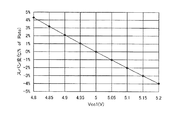
そして、定電圧源110による印加電圧VF1及びVF2とA/D変換器101の測定値との関係は図6に示すようになる。両者の関係がリニアな関係である範囲を、設計上はチップ温度+15〜+165℃に相当する電圧1.489〜2.103Vとし、A/D変換器101から出力される測定値を4.5〜0.5Vとする。この場合には、チップ温度155℃に相当する電圧VF1=1.5298V及びチップ温度25℃に相当する電圧値VF2=2.0619Vを印加した場合に、A/D変換器101から得られる測定値は、設計上はVF1=1.5298Vの時には、Vout1_s=4.233V、VF2=2.0619の時にはVout2_s=0.7667Vとなる。
The relationship between the voltages VF1 and VF2 applied by the constant voltage source 110 and the measured value of the A /
これら測定値Vout1_s及びVout2_sを結ぶ実線図示の線分S1−S2に基づいて、得られたAD変換器101の測定値Vout_sから入力値である電圧VFを逆算によって算出することができる。
このときの測定値Vout_sは、下記(9)式によって算出される。
Based on the line segment S1-S2 shown by the solid line connecting these measurement values Vout1_s and Vout2_s, the voltage VF as an input value can be calculated from the measurement value Vout_s of the obtained
The measured value Vout_s at this time is calculated by the following equation (9).
この(9)式において、右辺第2項の+Vout1_sがオフセット補正値となる。
この(9)式において、線分S1−S2の傾きをα12_sとすると、この傾きα12_sは、下記(10)式で表される。
α12_s={Vout2_s−Vout1_s}/(VF2−VF1)……(10)
したがって、上記(9)式を変形することにより、下記(11)式に示すように、得られた測定値Vout_sから入力値である電圧VFを算出することができる。
In this equation (9), + Vout1_s in the second term on the right side is the offset correction value.
In the equation (9), when the slope of the line segment S1-S2 is α12_s, the slope α12_s is expressed by the following equation (10).
α12_s = {Vout2_s−Vout1_s} / (VF2−VF1) (10)
Therefore, by modifying the above equation (9), as shown in the following equation (11), the voltage VF that is the input value can be calculated from the obtained measured value Vout_s.
この逆算によって求められた電圧VFかからチップ温度を算出するには、図2(b)に示す温度検出用ダイオードの温度と順方向電圧VFの関係を示す特性線図から求めることができる。すなわち、電圧VF=2.0619Vの時には、チップ温度Tc=25℃、電圧VF=1.5298Vの時には、チップ温度Tc=155℃となって、任意の電圧VFからチップ温度Tcを求めることができる。 In order to calculate the chip temperature from the voltage VF obtained by this reverse calculation, it can be obtained from the characteristic diagram showing the relationship between the temperature of the temperature detecting diode and the forward voltage VF shown in FIG. That is, when the voltage VF = 2.0619V, the chip temperature Tc = 25 ° C., and when the voltage VF = 1.5298V, the chip temperature Tc = 155 ° C., and the chip temperature Tc can be obtained from the arbitrary voltage VF. .
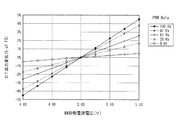
上記の説明は、回路定数が設計値そのもので、理想的な場合について行ったが、実際には、図3の電圧源Vcc1,Vcc2、A/D変換器101の基準電圧、抵抗値などのバラツキがあるので、図6に示す線分S1−S2にはならず、図6で一点鎖線図示のような線分S1−S2に対して偏移した線分M1−M2となる。
The above description has been made for an ideal case where the circuit constant is the design value itself. In practice, however, variations in the voltage sources Vcc1 and Vcc2, the reference voltage of the A /
すなわち、図5に示す定電圧源110からチップ温度155℃に相当する電圧値VF1及び25℃に相当する電圧値VF2を印加した時に、入力電圧VF1に対するA/D変換器101の設計上の測定値Vout1_s及び設計上の測定値Vout2_sを結ぶ線分S1−S2と、入力電圧VF1に対する実測の測定値Vout1_m及び実測の測定値Vout2_mを結ぶ線分M1−M2とに着目する。
That is, when the voltage value VF1 corresponding to the chip temperature 155 ° C. and the voltage value VF2 corresponding to 25 ° C. are applied from the constant voltage source 110 shown in FIG. 5, the design measurement of the A /
線分S1−S2と線分M1−M2とは、傾きとオフセット量が異なるので、測定された測定値Vout_mから、順方向電圧VFを逆算によって求める際に、線分S1−S2を用いると、得られた順方向電圧VFには、線分S1−S2及び線分M1−M2の相違による誤差を含んでしまう問題がある。このため、測定された測定値Vout_mから、順方向電圧VFを逆算によって算出する際に適用する線分をM1−M2になるように傾きとオフセット補正を行う必要がある。
そこで、実際のチップ温度検出回路13によって得られる線分M1−M2の特性を用いて、温度検出ダイオードDU2の任意の順方向電圧VFに対する測定値Vout_mは下記(12)式で表現される。
Since the line segment S1-S2 and the line segment M1-M2 have different slopes and offset amounts, when the line segment S1-S2 is used when calculating the forward voltage VF from the measured value Vout_m by back calculation, The obtained forward voltage VF has a problem that it includes an error due to a difference between the line segment S1-S2 and the line segment M1-M2. For this reason, it is necessary to perform inclination and offset correction so that the line segment applied when calculating the forward voltage VF by back calculation from the measured value Vout_m is M1-M2.
Therefore, using the characteristic of the line segment M1-M2 obtained by the actual chip
この(12)式において、傾きα12_mを下記(13)式のように設定すると、測定値Vout_mから温度検出用ダイオードDU2の順方向電圧VFは下記(14)式によって求められ、チップ温度検出回路の回路素子のバラツキを軽減した値が得られることになる。
α12_m={Vout2_m−Vout1_m}/(VF2−VF1)……(13)
In this equation (12), when the inclination α12_m is set as in the following equation (13), the forward voltage VF of the temperature detection diode DU2 is obtained from the measured value Vout_m by the following equation (14), and the chip temperature detection circuit A value with reduced variations in circuit elements can be obtained.
α12_m = {Vout2_m−Vout1_m} / (VF2−VF1) (13)
この(14)式で求められるチップ温度検出回路の回路素子のバラツキを軽減した温度検出用ダイオードの温度と順方向電圧VFから図2(b)の温度検出ダイオードの温度と順方向電圧の関係を表す特性線図から正確なチップ温度を求めることができる。
このようにして、設計に基づく(9)式及び(11)式を、実測値に基づく式(12)式及び(14)式に置換することは、線分S1−S2を線分M1−M2とすることであり、線分S1−S2に対して傾き補正及びオフセット補正を行ったこととなる。
The relationship between the temperature of the temperature detecting diode and the forward voltage in FIG. 2B is calculated from the temperature of the temperature detecting diode and the forward voltage VF in which the variation of the circuit elements of the chip temperature detecting circuit obtained by the equation (14) is reduced. An accurate chip temperature can be obtained from the characteristic diagram.
In this way, replacing the formulas (9) and (11) based on the design with the formulas (12) and (14) based on the actually measured values replaces the line segment S1-S2 with the line segment M1-M2. In other words, the inclination correction and the offset correction are performed on the line segment S1-S2.
このため、校正処理部107で、定電圧源110からチップ温度155℃に相当する電圧値VF1及び25℃に相当する電圧値VF2を印加して、A/D変換器101から出力される測定値Vout1_m及びVout2_mを読込み、前記(13)式の演算を行って線分M1−M2の傾きα12_mを算出し、この傾きα12_mとオフセット補正値Vout1_mとを不揮発性メモリ部106に記憶する。
Therefore, the
そして、チップ温度演算部108で、温度検出用ダイオードDU2を接続した状態でのA/D変換器101から出力される測定値Vout_mを読込み、この測定値Vout_mと不揮発性メモリ部106に記憶されている線分M1−M2の傾きα12_m及びオフセット補正値Vout1_mとを前記(14)式に代入して、温度検出用ダイオードDU2の順方向電圧VFを算出する。さらに、チップ温度演算部108で、算出した順方向電圧VFに基づいて図2(b)に示す特性線図を参照してチップ温度Tcを算出する。
The chip
そして、マイクロコンピュータ102の中央処理装置104では、図7に示す演算処理を実行する。
この演算処理は、図7に示すように、先ず、ステップS1で中央処理装置104に接続された例えばモーメンタリ式の校正処理開始スイッチ109がオン状態となったか否かを判定し、校正処理開始スイッチ109がオフ状態であるときにはオン状態となるまで待機し、校正処理開始スイッチ109がオン状態となると、ステップS2に移行する。
Then, the
As shown in FIG. 7, in this calculation process, first, in step S1, for example, it is determined whether or not a momentary type calibration process start
このステップS2では、定電圧源110に対して、チップ温度155℃に相当する電圧値VF1を印加する印加指令を出力してからステップS3に移行する。このステップS3では、印加した電圧VF1に相当する測定値がA/D変換器101から出力されるまでの所定時間が経過した後にA/D変換器101から出力される測定値Vout1_mを読込む。
In step S2, an application command for applying a voltage value VF1 corresponding to a chip temperature of 155 ° C. is output to the constant voltage source 110, and then the process proceeds to step S3. In step S3, the measurement value Vout1_m output from the A /
次いで、ステップS4に移行して、定電圧源110に対して、チップ温度25℃に相当する電圧値VF2を印加する印加指令を出力してからステップS5に移行する。このステップS5では、印加した電圧VF2に相当する測定値がA/D変換器101から出力されるまでの所定時間が経過した後にA/D変換器101から出力される測定値Vout2_mを読込んでからステップS6に移行する。
Next, the process proceeds to step S4, an application command for applying a voltage value VF2 corresponding to a chip temperature of 25 ° C. is output to the constant voltage source 110, and then the process proceeds to step S5. In this step S5, after reading a measurement value Vout2_m output from the A /
このステップS6では、読込んだ測定値Vout1_m及びVour2_mと、既知である電圧値VF1及びVF2とに基づいて前記(13)式の演算を行って線分M1−M2の傾きα12_mを算出してからステップS7に移行する。
このステップS7では、算出した線分M1−M2の傾きα12_mとオフセット補正値Vout1_mを不揮発性メモリ部106に格納してから校正処理を終了する。
In this step S6, after calculating the equation (13) based on the read measurement values Vout1_m and Vour2_m and the known voltage values VF1 and VF2, the slope α12_m of the line segment M1-M2 is calculated. The process proceeds to step S7.
In step S7, the calculated inclination α12_m of the line segment M1-M2 and the offset correction value Vout1_m are stored in the
チップ温度演算処理は、図8に示すように、所定時間毎のタイマ割込処理として実行される。このチップ温度演算処理では、先ず、ステップS11で、不揮発性メモリ部106に線分M1−M2の傾きα12_mとオフセット補正値Vout1_mとが格納されているか否かを判定する。この判定結果が、不揮発性メモリ部106に傾きα12_m及び測定値Vout1_mが格納されていないときには、そのままタイマ割込処理を終了して所定のメインプログラムに復帰する。
As shown in FIG. 8, the chip temperature calculation process is executed as a timer interrupt process at predetermined time intervals. In this chip temperature calculation process, first, in step S11, it is determined whether or not the slope α12_m of the line segment M1-M2 and the offset correction value Vout1_m are stored in the
ステップS11の判定結果が、不揮発性メモリ部106に傾きα12_m及び測定値Vout1_mが格納されているものであるときにはステップS12に移行して、A/D変換器101から出力される測定値Vout_mを読込む。
次いで、ステップS13に移行して、不揮発性メモリ部106に記憶されている線分M1−M2の傾きα12_mとオフセット補正値Vout1_mと、上記ステップS12で読込んだ測定値Vout_mとを前述した(14)式に代入して温度検出用ダイオードDU2の順方向電圧VFを算出する。
When the determination result in step S11 is that the inclination α12_m and the measured value Vout1_m are stored in the
Subsequently, the process proceeds to step S13, and the inclination α12_m of the line segment M1-M2 and the offset correction value Vout1_m stored in the
次いで、ステップS14に移行して、ステップS13で算出した順方向電圧VFをもとにROM等に記憶された図2(b)の温度と順方向電圧との関係を表すチップ温度算出テーブルを参照してチップ温度Tcを算出してからステップS15に移行する。
このステップS15では、ステップS14で算出したチップ温度Tcの表示情報を中央処理装置104に接続された液晶等の表示装置に出力してからタイマ割込処理を終了して所定のメインプログラムに復帰する。
ここで、図7の校正処理が図4における校正処理部107に対応し、図8のチップ温度算出処理が図4におけるチップ温度演算部108に対応している。
Next, the process proceeds to step S14, and the chip temperature calculation table showing the relationship between the temperature and the forward voltage in FIG. 2B stored in the ROM or the like based on the forward voltage VF calculated in step S13 is referred to. After calculating the chip temperature Tc, the process proceeds to step S15.
In step S15, the display information of the chip temperature Tc calculated in step S14 is output to a display device such as a liquid crystal connected to the
Here, the calibration process in FIG. 7 corresponds to the
次に、上記第1の実施形態の動作を説明する。
インテリジェントパワーモジュールの調整操作段階で、チップ温度検出回路13(又は14)の校正処理を行うには、先ず、図5に示すように、温度検出用ダイオードDU2(又はDD2)に代えて、電圧印加指令によって電圧値VF1及びVF2を出力可能な定電圧源110を接続する。
この状態で、マイクロコンピュータ102の校正処理開始スイッチ109をオン状態とすることにより、中央処理装置104で、図7に示す校正処理を実行開始させる。
この校正処理では、校正処理開始スイッチ109がオン状態となることにより、ステップS1からステップS2に移行して、定電圧源110に155℃に相当する電圧値VF1を印加する印加指令値を出力する。
Next, the operation of the first embodiment will be described.
In order to perform the calibration process of the chip temperature detection circuit 13 (or 14) at the adjustment operation stage of the intelligent power module, first, as shown in FIG. 5, a voltage application is performed instead of the temperature detection diode DU2 (or DD2). A constant voltage source 110 capable of outputting voltage values VF1 and VF2 is connected according to a command.
In this state, the calibration
In this calibration process, when the calibration process start
これにより、定電圧源110で電圧値VF1が温度検出用ダイオードDU2(又はDU19の接続端子に印加され、この電圧値VF1がパルス幅変調回路76のレベル変換器77でレベル変換されたレベル変換電圧VlevがコンパレータIC5に入力される。このコンパレータIC5には三角波発生器78から出力される三角波電圧Vtriが入力されているので、このコンパレータIC5からレベル変換電圧Vlevの電圧値に応じたデューティ比のパルス幅変調信号が出力される。このパルス幅変調信号が電界効果トランジスタ81を介し、フォトカプラ90を介してPWM−アナログ変換回路91に供給される。
As a result, the voltage value VF1 is applied to the temperature detection diode DU2 (or the connection terminal of the DU19) by the constant voltage source 110, and the voltage value VF1 is level-converted by the level converter 77 of the pulse width modulation circuit 76. Vlev is input to the
このPWM−アナログ変換回路91では、フォトカプラ90から入力されパルス幅変調信号に基づいて2値化回路で2値化信号を生成し、バッファ回路93でインピーダンス変換した後、ローパスフィルタ回路94で平滑化して直流レベルに変換される。
この直流レベル信号がA/D変換器101に入力されてデジタル変換されて測定値として出力される。
In this PWM-
This DC level signal is input to the A /
この電圧値VF1に対応する測定値Vout1_mが中央処理装置104に読込まれ(ステップS3)、次いで定電圧源110に対して25℃に相当する電圧値VF2を印加する電圧印加指令が出力される。
このため、定電圧源110から電圧値VF2が温度検出用ダイオードDU2(又はDD2)の接続端子に印加される。この印加された電圧VF2が上記と同様にしてパルス幅変調信号に変換されてからPWM−アナログ変換回路91で直流レベルに変換されてA/D変換器101から測定値Vout2_mとして出力され、これが中央処理装置104に読込まれる(ステップS5)。
The measured value Vout1_m corresponding to the voltage value VF1 is read into the central processing unit 104 (step S3), and then a voltage application command for applying the voltage value VF2 corresponding to 25 ° C. is output to the constant voltage source 110.
For this reason, the voltage value VF2 is applied from the constant voltage source 110 to the connection terminal of the temperature detection diode DU2 (or DD2). The applied voltage VF2 is converted into a pulse width modulation signal in the same manner as described above, and then converted into a DC level by the PWM-
そして、読込まれた測定値Vout1_m及びVout2_mと、既知の電圧値VF1及びVF2とに基づいて前記(13)式の演算を行って図6で一点鎖線図示の線分M1−M2の傾きα12_mを算出する(ステップS6)。
次いで、算出した線分M1−M2の傾きα12_mと測定値Vout1_m及びVout2_mの1つであるオフセット補正値Vout1_mとが不揮発性メモリ部106に格納され(ステップS7)、校正処理を終了する。
Based on the read measured values Vout1_m and Vout2_m and the known voltage values VF1 and VF2, the calculation of the equation (13) is performed to calculate the slope α12_m of the line segment M1-M2 shown in FIG. (Step S6).
Next, the calculated slope α12_m of the line segment M1-M2 and the offset correction value Vout1_m that is one of the measured values Vout1_m and Vout2_m are stored in the nonvolatile memory unit 106 (step S7), and the calibration process is terminated.
このように、校正処理によって不揮発性メモリ部106に、線分M1−M2の傾きα12_mとオフセット補正値Vout_mとが格納されると、定電圧源110を取り外して温度測定用ダイオードDU2(又はDD2)を接続してマイクロコンピュータ102を再起動する。
これによって、中央処理装置104で図8のチップ温度演算処理が実行され、不揮発性メモリ部106に線分M1−M2の傾きα12_m及びオフセット補正値Vout1_mが格納されているので、ステップS11からステップS12に移行して、A/D変換器101から出力される温度検出用ダイオードDU2(又はDD2)の順方向電圧VFに応じた測定値Vout_mを読込む。
As described above, when the inclination α12_m of the line segment M1-M2 and the offset correction value Vout_m are stored in the
As a result, the chip temperature calculation process of FIG. 8 is executed by the
次いで、読込んだ測定値Vout_mと、不揮発性メモリ部106に記憶されている線分M1−M2の傾きα12_m及びオフセット補正値Vout1_m、既知の電圧値VF1とを前記(14)式に代入して、温度検出用ダイオードDU2(又はDD2)の順方向電圧VFを算出する(ステップS13)。
次いで、算出した順方向電圧VFをもとに、図2(b)に示す順方向電圧算出テーブルを参照して、チップ温度Tcを算出し(ステップS14)、算出したチップ温度Tcを表示装置に表示し(ステップS15)、タイマ割込処理を終了する。
Next, the read measurement value Vout_m, the inclination α12_m of the line segment M1-M2 stored in the
Next, based on the calculated forward voltage VF, the chip temperature Tc is calculated with reference to the forward voltage calculation table shown in FIG. 2B (step S14), and the calculated chip temperature Tc is displayed on the display device. This is displayed (step S15), and the timer interrupt process is terminated.
このように、上記第1の実施形態によると、調整操作段階で、温度検出用ダイオードDU2(又はDD2)に代えて、定電圧源110を接続した状態で校正処理を行って、線分M1−M2の傾きα12_mを算出し、算出した傾きα12_mとオフセット補正値Vout1_mとを不揮発性メモリ部106に記憶する。
その後、温度検出用ダイオードDU2(又はDD2)を正規に接続した状態で、チップ温度演算処理を行うことにより、チップ温度検出回路13(又は14)の回路素子のバラツキを軽減したすなわち設計上の線分S1−S2に対して、傾き補正及びオフセット補正を行った正確なチップ温度Tcを得ることができる。
Thus, according to the first embodiment, in the adjustment operation stage, the calibration process is performed with the constant voltage source 110 connected in place of the temperature detection diode DU2 (or DD2), and the line segment M1- The inclination α12_m of M2 is calculated, and the calculated inclination α12_m and the offset correction value Vout1_m are stored in the
Thereafter, chip temperature calculation processing is performed in a state where the temperature detection diode DU2 (or DD2) is properly connected, thereby reducing variations in the circuit elements of the chip temperature detection circuit 13 (or 14), that is, a design line. It is possible to obtain an accurate chip temperature Tc in which the inclination correction and the offset correction are performed on the minute S1-S2.
しかも、不揮発性メモリ部106に線分M1−M2の傾きα12_mを演算してオフセット補正値Vout1_mとともに格納するようにしたので、チップ温度Tcの演算処理を容易に行うことができ、中央処理装置104の演算負荷を軽減することができる。
なお、上記第1の実施形態においては、A/D変換器101から出力される測定値Vout1_m、Vout2_m及びVout_mをそのまま演算処理に使用した場合について説明した。しかしながら、A/D変換器101から出力される測定値を取り込む際に、ノイズの影響を受ける場合がある。この場合には、A/D変換器101から出力される測定値のサンプリングを多数回行い、多数回のサンプリング値を加算平均処理して加算平均値を測定値Vout1_m、Vout2_m及びVout_mとして使用することにより、ノイズの影響を軽減することができる。
In addition, since the slope α12_m of the line segment M1-M2 is calculated in the
In the first embodiment, the case where the measurement values Vout1_m, Vout2_m, and Vout_m output from the A /
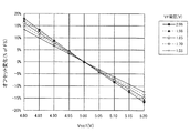
また、A/D変換器101の入力信号は、パルス幅変調(PEM)信号をローパスフィルタ回路94で平滑化された直流レベル信号であるが、微視的に見ると図9に示すように、数10mV程度の変動がある。このため、A/D変換器101で、図9に示すように、変動周期(パルス幅変調回路76における三角波発生器78の周波数)の任意の整数n倍のサンプリング期間でサンプリングを行い、サンプリング値の加算平均値を測定値Vout1_m、Vout2_m及びVout_mとして使用することにより、A/D変換器101の入力信号の変動の影響を軽減することができる。
Further, the input signal of the A /
次に、本発明の第2の実施形態を図10について説明する。
この第2の実施形態では、A/D変換器をマイクロコンピュータ102側に設ける場合に代えて温度検出用ダイオードの順方向電圧を直接デジタル変換するようにしたものである。
すなわち、第2の実施形態では、図10に示すように、温度検出用ダイオードDU2(又はDD2)の順方向電圧VFをA/D変換器120で直接デジタル変換して測定値を出力し、このA/D変換器120から出力される測定値を、低機能のマイクロコンピュータに搭載されるシリアル伝送ユニット130を介して電界効果トランジスタ81のゲートに供給するようにしている。
Next, a second embodiment of the present invention will be described with reference to FIG.
In this second embodiment, instead of providing an A / D converter on the
That is, in the second embodiment, as shown in FIG. 10, the forward voltage VF of the temperature detection diode DU2 (or DD2) is directly digitally converted by the A /
これに応じて、PWM−アナログ変換回路91が省略されて、2値化回路92のみが設けられ、この2値化回路92から出力される2値化信号が直接マイクロコンピュータ102のインタフェース回路103に入力されている。ここで、マイクロコンピュータ102の中央処理装置104で実行する校正処理及びチップ演算処理については、前述した第1の実施形態における図7及び図8の処理と同様の処理を行い、校正処理時に温度検出用ダイオードDU2(又はDD2)に代えて定電圧源110を温度検出用ダイオードDU2(又はDD2)の接続端子に接続して、校正処理を行う。
Accordingly, the PWM-
この第2の実施形態によると、温度検出用ダイオードDU2(又はDD2)の順方向電圧VFが直接A/D変換器120で測定値に変換されるので、この測定値をシリアル伝送ユニット130、電界効果トランジスタ81及びフォトカプラ90を介して2値化回路92で2値化信号に変換してマイクロコンピュータ102に供給するだけでよく、低機能のマイクロコンピュータに搭載されるシリアル伝送ユニット130をアーム側に搭載する必要はあるが、チップ温度検出回路13(又は14)の構成を簡略化することができる。
According to the second embodiment, the forward voltage VF of the temperature detection diode DU2 (or DD2) is directly converted into a measured value by the A /
なお、上記第1及び第2の実施形態においては、説明を省略したが、チップ温度検出回路13及び14の校正処理を行う場合に、制御回路3と各アーム1及び2のパワースイッチング素子SWU及びSWDとを接続する前に、チップ温度検出回路13及び14の温度検出用ダイオードDU2及びDD2を接続する接続端子に定電圧源110を接続して校正処理を行い、その後に制御回路3とパワースイッチング素子SWU及びSWDとを接続して、チップ温度の検出を行うようにすることが好ましい。
In the first and second embodiments, the description is omitted. However, when the calibration processing of the chip
また、上記第1及び第2の実施形態においては、校正処理で、不揮発性メモリ部106に線分M1−M2の傾きα12_m及びオフセット補正値Vout1_mを記憶する場合について説明した。本発明における不揮発性メモリ部106としてはフラッシュメモリ、EPROM、ROM等の任意の不揮発性記憶媒体を適用することができる他、常時電源を供給するRAM等を適用することもできる。要は、校正処理で算出した線分M1−M2の傾きα12_m及びオフセット補正値Vout1_mを読み出し可能に記憶していればよいものである。
また、上記第1及び第2の実施形態においては、オフセット補正値として測定値Vout1_mを適用したが、これに代えて測定値Vout2_mをオフセット補正値としてもよい。
In the first and second embodiments described above, the case where the inclination α12_m of the line segment M1-M2 and the offset correction value Vout1_m are stored in the
In the first and second embodiments, the measurement value Vout1_m is applied as the offset correction value. Instead, the measurement value Vout2_m may be used as the offset correction value.
1…上アーム、2…下アーム、3…制御回路、5,6…IGBT、7,8…ゲートドライバIC、9,10…IGBT保護回路、11,12…過電流検出部、SWU,SWD…パワースイッチング素子、DD2,DU2…温度検出用ダイオード、13,14…温度測定回路、70…定電流源、IC1…バッファアンプ、76…パルス幅変調回路、77…レベル変換器、78…三角波発生回路、IC3…コンパレータ、IC4…オペアンプ、IC5…コンパレータ、90…フォトカプラ、91…PWM−アナログ変換回路、92…2値化回路、93…バッファ回路、94…ローパスフィルタ回路、100…定電圧素子、101…A/D変換器、102…マイクロコンピュータ、103…インタフェース回路、104…中央処理装置、105…揮発性メモリ部、106…不揮発性メモリ部、107…校正処理部、108…チップ温度演算部、109…校正処理開始スイッチ、110…定電圧源、120…A/D変換器、130…シリアル伝送ユニット
DESCRIPTION OF
Claims (5)
前記チップ温度検出回路は、前記温度検出用ダイオードに定電流を供給する定電流源と、前記温度検出用ダイオードの両端の順方向電圧をデジタル変換して測定値として出力するA/D変換器と、該A/D変換器から出力される測定値が入力され、当該測定値に基づいて前記チップ温度を演算する演算処理部とを少なくとも備え、
前記演算処理部は、前記チップ温度検出回路の誤差の校正時に、前記温度検出用ダイオードに代えて既知の異なる複数の基準電圧値を印加する基準電圧源を接続し、前記複数の基準電圧値をそれぞれ印加したときの前記A/D変換器から出力される測定値を結ぶ線分の傾きを演算し、演算した線分の傾きと、前記A/D変換器から出力される測定値のうちの1つであるオフセット補正値とを記憶部に記憶する校正処理部と、前記温度検出用ダイオードによる温度測定時に、前記A/D変換器から出力される測定値と、前記記憶部に記憶されている線分の傾き及びオフセット補正値とに基づいて補正測定値を演算し、当該補正測定値に基づいて前記チップ温度を演算するチップ温度演算部とを備え、
前記校正処理部は、前記基準電圧を印加した時の前記A/D変換器から得られる測定値の測定を複数回行い、複数回の測定値の平均値を測定値とした
ことを特徴とするパワー半導体装置の温度測定装置。 A power semiconductor device temperature measurement device comprising a chip temperature detection circuit for detecting a chip temperature of the power switching element in a power semiconductor device provided with a power switching element and a temperature detection diode on a silicon chip,
The chip temperature detection circuit includes a constant current source that supplies a constant current to the temperature detection diode, an A / D converter that digitally converts a forward voltage at both ends of the temperature detection diode, and outputs the result as a measurement value; A measurement value output from the A / D converter is input, and at least an arithmetic processing unit that calculates the chip temperature based on the measurement value,
The arithmetic processing unit connects a reference voltage source that applies a plurality of known different reference voltage values instead of the temperature detection diode at the time of calibration of the error of the chip temperature detection circuit, and the plurality of reference voltage values are The slope of the line segment connecting the measurement values output from the A / D converter when applied is calculated, and the slope of the calculated line segment and the measurement value output from the A / D converter are calculated. A calibration processing unit that stores one offset correction value in the storage unit, a measurement value that is output from the A / D converter at the time of temperature measurement by the temperature detection diode, and a storage unit that is stored in the storage unit A chip temperature calculation unit that calculates a correction measurement value based on the slope of the line segment and the offset correction value, and calculates the chip temperature based on the correction measurement value ;
The calibration processing unit performs measurement of the measurement value obtained from the A / D converter when the reference voltage is applied a plurality of times, and sets an average value of the plurality of measurement values as a measurement value. A temperature measuring device for a power semiconductor device characterized by
前記チップ温度検出回路は、前記温度検出用ダイオードに定電流を供給する定電流源と、前記温度検出用ダイオードの両端の順方向電圧を入力信号としてパルス幅変調信号を出力するパルス幅変調回路と、該パルス幅変調回路から出力されるパルス幅変調信号を電気的に絶縁して伝送させる絶縁伝送回路と、該絶縁伝送回路の出力信号を平滑化するローパスフィルタと、該ローパスフィルタのフィルタ出力をデジタル変換して測定値として出力するA/D変換器と、該A/D変換器から出力される測定値が入力され、当該測定値に基づいて前記チップ温度を演算する演算処理部とを少なくとも備え、
前記演算処理部は、前記チップ温度検出回路の誤差の校正時に、前記温度検出用ダイオードに代えて既知の異なる複数の基準電圧値を印加する基準電圧源を接続し、前記複数の基準電圧値をそれぞれ印加したときの前記A/D変換器から出力される測定値を結ぶ線分の傾きを演算し、演算した線分の傾きと、前記A/D変換器から出力される測定値のうちの1つであるオフセット補正値とを記憶部に記憶する校正処理部と、前記温度検出用ダイオードによる温度測定時に、前記A/D変換器から出力される測定値と、前記記憶部に記憶されている線分の傾き及びオフセット補正値とに基づいて補正測定値を演算し、当該補正測定値に基づいて前記チップ温度を演算するチップ温度演算部とを備え、
前記校正処理部は、基準電圧を印加した時の前記A/D変換器から出力される測定値に対して、前記パルス幅変調回路に含まれる三角波発生回路の発振周期の整数倍の期間においてサンプリングを行い、サンプリング値の平均値を測定値とした
ことを特徴とするパワー半導体装置の温度測定装置。 A power semiconductor device temperature measurement device comprising a chip temperature detection circuit for detecting a chip temperature of the power switching element in a power semiconductor device provided with a power switching element and a temperature detection diode on a silicon chip,
The chip temperature detection circuit includes a constant current source that supplies a constant current to the temperature detection diode, a pulse width modulation circuit that outputs a pulse width modulation signal using a forward voltage across the temperature detection diode as an input signal, and An insulation transmission circuit for electrically insulating and transmitting the pulse width modulation signal output from the pulse width modulation circuit, a low-pass filter for smoothing the output signal of the insulation transmission circuit, and a filter output of the low-pass filter. At least an A / D converter that performs digital conversion and outputs a measurement value, and an arithmetic processing unit that receives the measurement value output from the A / D converter and calculates the chip temperature based on the measurement value Prepared,
The arithmetic processing unit connects a reference voltage source that applies a plurality of known different reference voltage values instead of the temperature detection diode at the time of calibration of the error of the chip temperature detection circuit, and the plurality of reference voltage values are The slope of the line segment connecting the measurement values output from the A / D converter when applied is calculated, and the slope of the calculated line segment and the measurement value output from the A / D converter are calculated. A calibration processing unit that stores one offset correction value in the storage unit, a measurement value that is output from the A / D converter at the time of temperature measurement by the temperature detection diode, and a storage unit that is stored in the storage unit A chip temperature calculation unit that calculates a correction measurement value based on the slope of the line segment and the offset correction value, and calculates the chip temperature based on the correction measurement value;
The calibration processing unit samples the measurement value output from the A / D converter when a reference voltage is applied in a period that is an integral multiple of the oscillation period of the triangular wave generation circuit included in the pulse width modulation circuit. was carried out, the temperature measuring device features and to Rupa Wah semiconductor device that the average value of the sampling values and the measured values.
されていることを特徴とする請求項4に記載のパワー半導体装置の温度測定装置。 In the calibration processing unit, two points at both ends of a plurality of known different reference voltage values are set to a value equivalent to or close to the forward voltage value of the temperature detection diode at the maximum and minimum temperatures of the chip temperature measurement range. temperature measuring apparatus of a power semiconductor device according to claim 4, characterized in that it is set <br/>.
Priority Applications (3)
| Application Number | Priority Date | Filing Date | Title |
|---|---|---|---|
| JP2011194942A JP5786571B2 (en) | 2011-09-07 | 2011-09-07 | Power semiconductor device temperature measurement device |
| CN201210327790.5A CN102998017B (en) | 2011-09-07 | 2012-09-06 | The temperature measurement equipment of power semiconductor arrangement |
| US13/607,017 US9562812B2 (en) | 2011-09-07 | 2012-09-07 | Temperature measuring device of a power semiconductor apparatus |
Applications Claiming Priority (1)
| Application Number | Priority Date | Filing Date | Title |
|---|---|---|---|
| JP2011194942A JP5786571B2 (en) | 2011-09-07 | 2011-09-07 | Power semiconductor device temperature measurement device |
Publications (2)
| Publication Number | Publication Date |
|---|---|
| JP2013057550A JP2013057550A (en) | 2013-03-28 |
| JP5786571B2 true JP5786571B2 (en) | 2015-09-30 |
Family
ID=47753793
Family Applications (1)
| Application Number | Title | Priority Date | Filing Date |
|---|---|---|---|
| JP2011194942A Expired - Fee Related JP5786571B2 (en) | 2011-09-07 | 2011-09-07 | Power semiconductor device temperature measurement device |
Country Status (3)
| Country | Link |
|---|---|
| US (1) | US9562812B2 (en) |
| JP (1) | JP5786571B2 (en) |
| CN (1) | CN102998017B (en) |
Families Citing this family (51)
| Publication number | Priority date | Publication date | Assignee | Title |
|---|---|---|---|---|
| JP4807352B2 (en) * | 2007-12-25 | 2011-11-02 | 三菱電機株式会社 | Temperature detection system |
| CN103843460B (en) * | 2011-10-12 | 2016-04-13 | Dialog半导体有限公司 | For the controller of Solid-state light bulb assembly |
| US9250137B2 (en) | 2012-09-21 | 2016-02-02 | Silicon Laboratories Inc. | Temperature measurement circuitry and system |
| CN103245435B (en) * | 2013-05-30 | 2015-07-29 | 上海贝岭股份有限公司 | For temperature calibration instrument and the method for CMOS temperature transmitter |
| KR101526680B1 (en) * | 2013-08-30 | 2015-06-05 | 현대자동차주식회사 | Temperature sensing circuit for igbt module |
| CN104458034B (en) * | 2013-09-22 | 2019-03-15 | 中兴通讯股份有限公司 | Temperature checking method and temperature-detecting device |
| CN103528714B (en) * | 2013-09-27 | 2016-11-02 | 上海贝岭股份有限公司 | The temperature calibration instrument of integrated CMOS temperature sensor and method |
| CN104515611B (en) * | 2013-09-29 | 2019-05-31 | 中兴通讯股份有限公司 | A kind of temperature-sensitive circuit and temperature sensor |
| WO2015084410A1 (en) * | 2013-12-06 | 2015-06-11 | Intel Corporation | Method and apparatus for calibrating a sensor |
| CN103759847B (en) * | 2014-01-25 | 2016-08-17 | 深圳清华大学研究院 | Junction temperature of light emitting diode detection device and detection method thereof |
| US10132696B2 (en) | 2014-07-11 | 2018-11-20 | Infineon Technologies Ag | Integrated temperature sensor for discrete semiconductor devices |
| DE112015005998T5 (en) | 2015-01-20 | 2017-10-05 | Mitsubishi Electric Corporation | SEMICONDUCTOR DEVICE |
| JP6319126B2 (en) * | 2015-02-05 | 2018-05-09 | 株式会社デンソー | Temperature correction circuit and temperature sensing element detection temperature correction method |
| US10247616B2 (en) | 2015-03-05 | 2019-04-02 | Renesas Electronics Corporation | Electronics device |
| JP6557136B2 (en) * | 2015-03-05 | 2019-08-07 | ルネサスエレクトロニクス株式会社 | Electronic equipment |
| CN104880225A (en) * | 2015-06-10 | 2015-09-02 | 河南科技学院 | Internet-of-things-based sensing system for crop planting field microclimate information |
| CN106339011A (en) * | 2015-07-10 | 2017-01-18 | 深圳市中兴微电子技术有限公司 | Chip temperature detection and control method and device |
| CN105628246A (en) * | 2015-12-20 | 2016-06-01 | 常州瑞华电力电子器件有限公司 | Power semiconductor module temperature monitoring system |
| KR101889780B1 (en) * | 2016-03-03 | 2018-09-28 | 주식회사 바스맨테크놀러지 | Dual Thermistor Sensing Circuit for high Accuracy Temperature |
| JP6637374B2 (en) * | 2016-04-27 | 2020-01-29 | ルネサスエレクトロニクス株式会社 | Semiconductor device and temperature sensor |
| US10802053B2 (en) * | 2016-09-22 | 2020-10-13 | Infineon Technologies Ag | Configuration of integrated current flow sensor |
| US10386189B2 (en) | 2016-10-04 | 2019-08-20 | Qualcomm Incorporated | Utilizing processing units to control temperature |
| EP3336499B1 (en) * | 2016-12-16 | 2019-12-11 | Mitsubishi Electric R & D Centre Europe B.V. | Method for controlling the temperature of a multi-die power module |
| TWI620407B (en) * | 2016-12-23 | 2018-04-01 | Actron Technology Corporation | Rectifier package module for vehicle and connection status detection method for temperature sensor thereof |
| CN107144778A (en) * | 2017-05-16 | 2017-09-08 | 珠海格力节能环保制冷技术研究中心有限公司 | A kind of chip temperature detection means and method |
| JP6764834B2 (en) | 2017-06-23 | 2020-10-07 | 日立オートモティブシステムズ株式会社 | Detector and power converter |
| DE102017212113A1 (en) * | 2017-07-14 | 2019-01-17 | Continental Teves Ag & Co. Ohg | Control arrangement, vehicle control unit and corresponding method and use |
| JP6958307B2 (en) * | 2017-12-08 | 2021-11-02 | トヨタ自動車株式会社 | Boost converter device and its control method |
| US10256024B1 (en) | 2018-01-15 | 2019-04-09 | Ford Global Technologies, Llc | Power converter temperature estimation |
| CN108768515B (en) * | 2018-05-24 | 2020-01-31 | 武汉华工正源光子技术有限公司 | Burst received optical power calibration method and device |
| JP7200522B2 (en) * | 2018-07-12 | 2023-01-10 | 株式会社デンソー | gate drive circuit |
| JP7205091B2 (en) * | 2018-07-18 | 2023-01-17 | 富士電機株式会社 | semiconductor equipment |
| CN109100052B (en) * | 2018-09-30 | 2024-03-12 | 深圳众城卓越科技有限公司 | PT100 temperature sensor's detection circuitry |
| KR20210015261A (en) * | 2019-08-01 | 2021-02-10 | 현대자동차주식회사 | Overcurrent detection reference compensation system of switching element for inverter and overcurrent detection system using the same |
| KR20210032111A (en) | 2019-09-16 | 2021-03-24 | 삼성전자주식회사 | Semiconductor memory device and memory system having the same |
| CN110896105A (en) * | 2019-11-29 | 2020-03-20 | 广东芯聚能半导体有限公司 | Power diode assembly and power diode protection method |
| GB2590976B (en) * | 2020-01-13 | 2022-04-20 | Nokia Technologies Oy | Semiconductor based temperature sensor |
| JP7427996B2 (en) * | 2020-02-13 | 2024-02-06 | 富士電機株式会社 | Testing method for semiconductor devices |
| JP7419948B2 (en) * | 2020-04-16 | 2024-01-23 | 株式会社デンソー | Internal combustion engine ignition system |
| CN113870917B (en) * | 2020-06-30 | 2023-09-12 | 长鑫存储技术有限公司 | Semiconductor device with a semiconductor device having a plurality of semiconductor chips |
| EP3965105B1 (en) | 2020-07-17 | 2024-02-07 | Changxin Memory Technologies, Inc. | Calibration of temperature detection module in semiconductor memory comprising a plurality of memory chips |
| KR20220130826A (en) | 2020-07-17 | 2022-09-27 | 창신 메모리 테크놀로지즈 아이엔씨 | semiconductor device |
| EP3968324B1 (en) * | 2020-07-17 | 2023-07-05 | Changxin Memory Technologies, Inc. | Semiconductor device |
| CN111933070A (en) * | 2020-07-27 | 2020-11-13 | 重庆惠科金渝光电科技有限公司 | Drive circuit and display device |
| US11764209B2 (en) * | 2020-10-19 | 2023-09-19 | MW RF Semiconductors, LLC | Power semiconductor device with forced carrier extraction and method of manufacture |
| CN112486224B (en) * | 2020-12-10 | 2022-03-18 | 安徽环瑞电热器材有限公司 | Bathroom equipment temperature control system and temperature control method thereof |
| CN112815819B (en) * | 2020-12-31 | 2022-12-30 | 大族激光科技产业集团股份有限公司 | Distance measuring device with temperature compensation function and cutting system |
| JP2022121034A (en) * | 2021-02-08 | 2022-08-19 | 富士電機株式会社 | Power conversion device |
| CN113050176B (en) * | 2021-03-10 | 2024-06-18 | 维沃移动通信有限公司 | Proximity detection circuit, electronic device, proximity detection processing method and device |
| JP7183337B2 (en) * | 2021-05-11 | 2022-12-05 | 三菱電機株式会社 | Temperature sensing system and temperature sensing circuit |
| CN115166459A (en) * | 2022-06-28 | 2022-10-11 | 中国第一汽车股份有限公司 | Junction temperature detection device, junction temperature detection method, electronic equipment and storage medium |
Family Cites Families (15)
| Publication number | Priority date | Publication date | Assignee | Title |
|---|---|---|---|---|
| JPH0755588A (en) * | 1993-08-10 | 1995-03-03 | Fujitsu Ltd | Temperature detector |
| JP3358459B2 (en) * | 1996-09-12 | 2002-12-16 | 株式会社デンソー | Temperature detection circuit |
| DE10029446A1 (en) * | 2000-06-21 | 2002-01-03 | Braun Gmbh | Method and circuit arrangement for measuring a voltage and / or a temperature |
| US7132868B2 (en) | 2001-06-27 | 2006-11-07 | Mitsubishi Denki Kabushiki Kaisha | Semiconductor device |
| JP2005333667A (en) | 2001-06-27 | 2005-12-02 | Mitsubishi Electric Corp | Semiconductor apparatus |
| JP2004117111A (en) | 2002-09-25 | 2004-04-15 | Toshiba Corp | Semiconductor device |
| US7427158B2 (en) * | 2005-01-13 | 2008-09-23 | Kabushiki Kaisha Toshiba | Advanced thermal sensor |
| JP4141444B2 (en) * | 2005-01-25 | 2008-08-27 | 三菱電機株式会社 | In-vehicle engine controller |
| AU2005336596B2 (en) * | 2005-09-21 | 2009-06-11 | Mitsubishi Denki Kabushiki Kaisha | Excessive-temperature detection system of motor controller |
| US7522434B2 (en) * | 2005-10-27 | 2009-04-21 | Wisconsin Alumni Research Foundation | Temperature estimation based on a signal oscillation |
| JP4229945B2 (en) | 2006-01-05 | 2009-02-25 | 三菱電機株式会社 | In-vehicle electronic control unit |
| JP2008116233A (en) | 2006-11-01 | 2008-05-22 | Hitachi Ltd | Motor drive device |
| JP4816489B2 (en) * | 2007-02-14 | 2011-11-16 | 株式会社デンソー | Calibration device for sensor built-in device |
| JP4886562B2 (en) * | 2007-03-19 | 2012-02-29 | 本田技研工業株式会社 | Power converter and multi-input / output power converter |
| US8674544B2 (en) * | 2009-01-26 | 2014-03-18 | Geneva Cleantech, Inc. | Methods and apparatus for power factor correction and reduction of distortion in and noise in a power supply delivery network |
-
2011
- 2011-09-07 JP JP2011194942A patent/JP5786571B2/en not_active Expired - Fee Related
-
2012
- 2012-09-06 CN CN201210327790.5A patent/CN102998017B/en not_active Expired - Fee Related
- 2012-09-07 US US13/607,017 patent/US9562812B2/en active Active
Also Published As
| Publication number | Publication date |
|---|---|
| US20130060499A1 (en) | 2013-03-07 |
| US9562812B2 (en) | 2017-02-07 |
| CN102998017B (en) | 2016-12-21 |
| JP2013057550A (en) | 2013-03-28 |
| CN102998017A (en) | 2013-03-27 |
Similar Documents
| Publication | Publication Date | Title |
|---|---|---|
| JP5786571B2 (en) | Power semiconductor device temperature measurement device | |
| US9035624B1 (en) | Power supply circuitry and current measurement | |
| JP6081718B2 (en) | Current compensation method for pulse width modulation converter for environmentally friendly vehicles | |
| JP4882706B2 (en) | Device for measuring input / output characteristics of analog circuit including operational amplifier and method for measuring input / output characteristics of analog circuit including operational amplifier | |
| US9776522B2 (en) | Wireless power supply system and power transmission device | |
| US8878583B2 (en) | PWM duty cycle converter | |
| JP6247034B2 (en) | CONVERTER DEVICE, FUEL CELL SYSTEM INCLUDING THE SAME, CONVERTER DEVICE CONTROL METHOD AND CONTROL DEVICE | |
| US8988899B2 (en) | Switching regulator device | |
| JPH0962387A (en) | Method and device for power control of battery power source and battery power source system | |
| US20110025248A1 (en) | Multi-phase dc/dc boost converter | |
| US9641071B2 (en) | Cuk based current source | |
| JP5360019B2 (en) | Power semiconductor device temperature measurement device | |
| JP2004208342A (en) | Power generation controller for vehicle | |
| JP2009207239A (en) | Charging controller for solar cells | |
| US20120217944A1 (en) | Current detector of inductive load | |
| US7312597B2 (en) | Actuation circuit for a switch in a switch-mode converter for improving the response to sudden changes | |
| JP4450792B2 (en) | Power saving effect display device in inverter device | |
| US8115458B2 (en) | Driver | |
| US20120013312A1 (en) | Power Control Device and Method thereof | |
| JP5141122B2 (en) | Switching power supply | |
| JP2006242610A (en) | Single power source voltage measuring circuit | |
| JP4848856B2 (en) | Digital / analog converter | |
| JP4967738B2 (en) | Method for adjusting input / output characteristics of analog circuit including operational amplifier | |
| JP2012157145A (en) | Bidirectional converter, control circuit thereof, and control method thereof | |
| JPWO2017126104A1 (en) | INVERTER DEVICE AND INVERTER DEVICE CONTROL METHOD |
Legal Events
| Date | Code | Title | Description |
|---|---|---|---|
| A621 | Written request for application examination |
Free format text: JAPANESE INTERMEDIATE CODE: A621 Effective date: 20140616 |
|
| A977 | Report on retrieval |
Free format text: JAPANESE INTERMEDIATE CODE: A971007 Effective date: 20150304 |
|
| A131 | Notification of reasons for refusal |
Free format text: JAPANESE INTERMEDIATE CODE: A131 Effective date: 20150428 |
|
| A521 | Request for written amendment filed |
Free format text: JAPANESE INTERMEDIATE CODE: A523 Effective date: 20150615 |
|
| TRDD | Decision of grant or rejection written | ||
| A01 | Written decision to grant a patent or to grant a registration (utility model) |
Free format text: JAPANESE INTERMEDIATE CODE: A01 Effective date: 20150630 |
|
| A61 | First payment of annual fees (during grant procedure) |
Free format text: JAPANESE INTERMEDIATE CODE: A61 Effective date: 20150713 |
|
| R150 | Certificate of patent or registration of utility model |
Ref document number: 5786571 Country of ref document: JP Free format text: JAPANESE INTERMEDIATE CODE: R150 |
|
| R250 | Receipt of annual fees |
Free format text: JAPANESE INTERMEDIATE CODE: R250 |
|
| R250 | Receipt of annual fees |
Free format text: JAPANESE INTERMEDIATE CODE: R250 |
|
| R250 | Receipt of annual fees |
Free format text: JAPANESE INTERMEDIATE CODE: R250 |
|
| R250 | Receipt of annual fees |
Free format text: JAPANESE INTERMEDIATE CODE: R250 |
|
| R250 | Receipt of annual fees |
Free format text: JAPANESE INTERMEDIATE CODE: R250 |
|
| LAPS | Cancellation because of no payment of annual fees |