JP5774701B2 - 液晶光学素子及び画像表示装置 - Google Patents
液晶光学素子及び画像表示装置 Download PDFInfo
- Publication number
- JP5774701B2 JP5774701B2 JP2013525528A JP2013525528A JP5774701B2 JP 5774701 B2 JP5774701 B2 JP 5774701B2 JP 2013525528 A JP2013525528 A JP 2013525528A JP 2013525528 A JP2013525528 A JP 2013525528A JP 5774701 B2 JP5774701 B2 JP 5774701B2
- Authority
- JP
- Japan
- Prior art keywords
- liquid crystal
- electrode
- region
- electrodes
- voltage
- Prior art date
- Legal status (The legal status is an assumption and is not a legal conclusion. Google has not performed a legal analysis and makes no representation as to the accuracy of the status listed.)
- Expired - Fee Related
Links
Images


Classifications
-
- G—PHYSICS
- G02—OPTICS
- G02B—OPTICAL ELEMENTS, SYSTEMS OR APPARATUS
- G02B30/00—Optical systems or apparatus for producing three-dimensional [3D] effects, e.g. stereoscopic images
- G02B30/20—Optical systems or apparatus for producing three-dimensional [3D] effects, e.g. stereoscopic images by providing first and second parallax images to an observer's left and right eyes
- G02B30/26—Optical systems or apparatus for producing three-dimensional [3D] effects, e.g. stereoscopic images by providing first and second parallax images to an observer's left and right eyes of the autostereoscopic type
- G02B30/27—Optical systems or apparatus for producing three-dimensional [3D] effects, e.g. stereoscopic images by providing first and second parallax images to an observer's left and right eyes of the autostereoscopic type involving lenticular arrays
-
- G—PHYSICS
- G02—OPTICS
- G02F—OPTICAL DEVICES OR ARRANGEMENTS FOR THE CONTROL OF LIGHT BY MODIFICATION OF THE OPTICAL PROPERTIES OF THE MEDIA OF THE ELEMENTS INVOLVED THEREIN; NON-LINEAR OPTICS; FREQUENCY-CHANGING OF LIGHT; OPTICAL LOGIC ELEMENTS; OPTICAL ANALOGUE/DIGITAL CONVERTERS
- G02F1/00—Devices or arrangements for the control of the intensity, colour, phase, polarisation or direction of light arriving from an independent light source, e.g. switching, gating or modulating; Non-linear optics
- G02F1/01—Devices or arrangements for the control of the intensity, colour, phase, polarisation or direction of light arriving from an independent light source, e.g. switching, gating or modulating; Non-linear optics for the control of the intensity, phase, polarisation or colour
- G02F1/13—Devices or arrangements for the control of the intensity, colour, phase, polarisation or direction of light arriving from an independent light source, e.g. switching, gating or modulating; Non-linear optics for the control of the intensity, phase, polarisation or colour based on liquid crystals, e.g. single liquid crystal display cells
- G02F1/133—Constructional arrangements; Operation of liquid crystal cells; Circuit arrangements
- G02F1/1333—Constructional arrangements; Manufacturing methods
- G02F1/1343—Electrodes
- G02F1/134309—Electrodes characterised by their geometrical arrangement
-
- G—PHYSICS
- G02—OPTICS
- G02B—OPTICAL ELEMENTS, SYSTEMS OR APPARATUS
- G02B3/00—Simple or compound lenses
- G02B3/12—Fluid-filled or evacuated lenses
- G02B3/14—Fluid-filled or evacuated lenses of variable focal length
-
- G—PHYSICS
- G02—OPTICS
- G02B—OPTICAL ELEMENTS, SYSTEMS OR APPARATUS
- G02B30/00—Optical systems or apparatus for producing three-dimensional [3D] effects, e.g. stereoscopic images
- G02B30/20—Optical systems or apparatus for producing three-dimensional [3D] effects, e.g. stereoscopic images by providing first and second parallax images to an observer's left and right eyes
- G02B30/22—Optical systems or apparatus for producing three-dimensional [3D] effects, e.g. stereoscopic images by providing first and second parallax images to an observer's left and right eyes of the stereoscopic type
- G02B30/25—Optical systems or apparatus for producing three-dimensional [3D] effects, e.g. stereoscopic images by providing first and second parallax images to an observer's left and right eyes of the stereoscopic type using polarisation techniques
-
- G—PHYSICS
- G02—OPTICS
- G02B—OPTICAL ELEMENTS, SYSTEMS OR APPARATUS
- G02B30/00—Optical systems or apparatus for producing three-dimensional [3D] effects, e.g. stereoscopic images
- G02B30/20—Optical systems or apparatus for producing three-dimensional [3D] effects, e.g. stereoscopic images by providing first and second parallax images to an observer's left and right eyes
- G02B30/26—Optical systems or apparatus for producing three-dimensional [3D] effects, e.g. stereoscopic images by providing first and second parallax images to an observer's left and right eyes of the autostereoscopic type
- G02B30/27—Optical systems or apparatus for producing three-dimensional [3D] effects, e.g. stereoscopic images by providing first and second parallax images to an observer's left and right eyes of the autostereoscopic type involving lenticular arrays
- G02B30/28—Optical systems or apparatus for producing three-dimensional [3D] effects, e.g. stereoscopic images by providing first and second parallax images to an observer's left and right eyes of the autostereoscopic type involving lenticular arrays involving active lenticular arrays
-
- G—PHYSICS
- G02—OPTICS
- G02B—OPTICAL ELEMENTS, SYSTEMS OR APPARATUS
- G02B30/00—Optical systems or apparatus for producing three-dimensional [3D] effects, e.g. stereoscopic images
- G02B30/20—Optical systems or apparatus for producing three-dimensional [3D] effects, e.g. stereoscopic images by providing first and second parallax images to an observer's left and right eyes
- G02B30/26—Optical systems or apparatus for producing three-dimensional [3D] effects, e.g. stereoscopic images by providing first and second parallax images to an observer's left and right eyes of the autostereoscopic type
- G02B30/30—Optical systems or apparatus for producing three-dimensional [3D] effects, e.g. stereoscopic images by providing first and second parallax images to an observer's left and right eyes of the autostereoscopic type involving parallax barriers
- G02B30/31—Optical systems or apparatus for producing three-dimensional [3D] effects, e.g. stereoscopic images by providing first and second parallax images to an observer's left and right eyes of the autostereoscopic type involving parallax barriers involving active parallax barriers
-
- G—PHYSICS
- G02—OPTICS
- G02F—OPTICAL DEVICES OR ARRANGEMENTS FOR THE CONTROL OF LIGHT BY MODIFICATION OF THE OPTICAL PROPERTIES OF THE MEDIA OF THE ELEMENTS INVOLVED THEREIN; NON-LINEAR OPTICS; FREQUENCY-CHANGING OF LIGHT; OPTICAL LOGIC ELEMENTS; OPTICAL ANALOGUE/DIGITAL CONVERTERS
- G02F1/00—Devices or arrangements for the control of the intensity, colour, phase, polarisation or direction of light arriving from an independent light source, e.g. switching, gating or modulating; Non-linear optics
- G02F1/01—Devices or arrangements for the control of the intensity, colour, phase, polarisation or direction of light arriving from an independent light source, e.g. switching, gating or modulating; Non-linear optics for the control of the intensity, phase, polarisation or colour
- G02F1/13—Devices or arrangements for the control of the intensity, colour, phase, polarisation or direction of light arriving from an independent light source, e.g. switching, gating or modulating; Non-linear optics for the control of the intensity, phase, polarisation or colour based on liquid crystals, e.g. single liquid crystal display cells
- G02F1/133—Constructional arrangements; Operation of liquid crystal cells; Circuit arrangements
- G02F1/1333—Constructional arrangements; Manufacturing methods
- G02F1/1343—Electrodes
- G02F1/134309—Electrodes characterised by their geometrical arrangement
- G02F1/134363—Electrodes characterised by their geometrical arrangement for applying an electric field parallel to the substrate, i.e. in-plane switching [IPS]
-
- G—PHYSICS
- G02—OPTICS
- G02F—OPTICAL DEVICES OR ARRANGEMENTS FOR THE CONTROL OF LIGHT BY MODIFICATION OF THE OPTICAL PROPERTIES OF THE MEDIA OF THE ELEMENTS INVOLVED THEREIN; NON-LINEAR OPTICS; FREQUENCY-CHANGING OF LIGHT; OPTICAL LOGIC ELEMENTS; OPTICAL ANALOGUE/DIGITAL CONVERTERS
- G02F1/00—Devices or arrangements for the control of the intensity, colour, phase, polarisation or direction of light arriving from an independent light source, e.g. switching, gating or modulating; Non-linear optics
- G02F1/29—Devices or arrangements for the control of the intensity, colour, phase, polarisation or direction of light arriving from an independent light source, e.g. switching, gating or modulating; Non-linear optics for the control of the position or the direction of light beams, i.e. deflection
-
- G—PHYSICS
- G02—OPTICS
- G02F—OPTICAL DEVICES OR ARRANGEMENTS FOR THE CONTROL OF LIGHT BY MODIFICATION OF THE OPTICAL PROPERTIES OF THE MEDIA OF THE ELEMENTS INVOLVED THEREIN; NON-LINEAR OPTICS; FREQUENCY-CHANGING OF LIGHT; OPTICAL LOGIC ELEMENTS; OPTICAL ANALOGUE/DIGITAL CONVERTERS
- G02F1/00—Devices or arrangements for the control of the intensity, colour, phase, polarisation or direction of light arriving from an independent light source, e.g. switching, gating or modulating; Non-linear optics
- G02F1/01—Devices or arrangements for the control of the intensity, colour, phase, polarisation or direction of light arriving from an independent light source, e.g. switching, gating or modulating; Non-linear optics for the control of the intensity, phase, polarisation or colour
- G02F1/13—Devices or arrangements for the control of the intensity, colour, phase, polarisation or direction of light arriving from an independent light source, e.g. switching, gating or modulating; Non-linear optics for the control of the intensity, phase, polarisation or colour based on liquid crystals, e.g. single liquid crystal display cells
- G02F1/133—Constructional arrangements; Operation of liquid crystal cells; Circuit arrangements
- G02F1/1333—Constructional arrangements; Manufacturing methods
- G02F1/1343—Electrodes
- G02F1/134309—Electrodes characterised by their geometrical arrangement
- G02F1/134381—Hybrid switching mode, i.e. for applying an electric field with components parallel and orthogonal to the substrates
Description
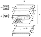
図1は、第1実施形態に係る画像表示装置10の模式図である。画像表示装置10は、2次元画像を表示可能な画像表示部11、偏光板12、屈折率分布型液晶光学素子としての液晶GRINレンズ20、第1電圧制御部50、及び第2電圧制御部51を備えている。画像表示部11は、画素がマトリクス状に配列された、所謂フラットパネルディスプレイ(FPD)が好ましく、そのような画像表示部として、非発光型の液晶ディスプレイ(LCD)、発光型のプラズマディスプレイ(PDP:Plasma Display Panel)、発光型の有機EL(electroluminescence)ディスプレイなどが用いられる。非発光型のディスプレイは、バックライトを有し、このバックライトからの光線を用いて画像を表示する。
次に、液晶GRINレンズ20の動作について説明する。液晶GRINレンズ20の電圧制御は、図1に示した第1電圧制御部50及び第2電圧制御部51によって行われる。第1電圧制御部50は、複数の引出線32(又は引出線33)のそれぞれに電気的に接続され、複数の引出線32をそれぞれ独立して電圧制御できるように構成されている。第2電圧制御部51は、第2電極40に電気的に接続され、第2電極40を電圧制御する。
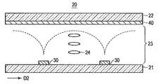
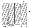
以上詳述したように第1実施形態では、液晶GRINレンズ20は、対向配置された一対の透明基板21及び22と、透明基板21及び22間に設けられた液晶層23と、液晶層23側の透明基板21上に設けられ、第1方向D1に沿って配列された複数の第1電極30と、液晶層23側の透明基板22上に設けられた第2電極40とを具備する。そして、複数の第1電極30は、第1方向D1と異なる第2方向D2に沿って配列された複数の第1電極領域31に分割される。また、各第1電極領域31に含まれる所定数の第1電極30は、引出線32によって電気的に接続されるようにしている。
第1電極領域31の境界(すなわち、引出線32のライン)は、レンズの境界(すなわち、第1電極30のライン)とは独立して設定される。そして、本実施形態では、第1電極領域31を単位として、レンズ機能のオン/オフを切り替えることが可能となる。これにより、第2方向D2に直交する方向に対して傾いた斜めレンズアレイを構成する液晶GRINレンズ20において、レンズの境界に束縛されることなく、矩形領域を単位として、部分的に2D表示と3D表示との切り替えを実現することができる。
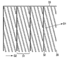
第2実施形態は、複数の第1電極30を電気的に接続する引出線32の他の構成例について示している。本実施形態の液晶光学素子である液晶GRINレンズ20においては、第1実施形態と比較して、引出線32の配置が異なる。図5は、第2実施形態に係る複数の第1電極30の平面図である。
本実施形態におけるその他の効果は、第1実施形態と同様である。
第3実施形態は、複数の第1電極30を電気的に接続する引出線32のさらに他の構成例について示している。本実施形態の液晶光学素子である液晶GRINレンズ20においては、第2実施形態と比較して、引出線32の配置が異なる。図6は、第3実施形態に係る複数の第1電極30の平面図である。
本実施形態におけるその他の効果は、第2実施形態と同様である。
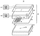
第4実施形態は、透明基板22上に設けられる第2電極40を複数に分割して形成し、2D/3D表示を切り替える領域の単位を、第1実施形態に比べて小さく制御できるようにしている。図7は、第4実施形態に係る画像表示装置10の模式図である。図8は、液晶GRINレンズ20を構成する第1電極30及び第2電極40の平面図である。
|V1on−V2off|<Vth
|V1off−V2on|<Vth
|V1off−V2off|<Vth
図9は、部分的に3D表示させるための電圧関係の一例を示す図である。一例として、図9の破線で示した領域、すなわち中央の4つの分割領域のみを3D表示にする場合について説明する。この例の場合、第1電圧制御部50は、第1電極30−2及び30−3にそれぞれ電圧V1onを印加し、それ以外の第1電極30−1及び30−4にそれぞれ電圧V1offを印加する。また、第2電圧制御部51は、第2電極40−2及び40−3にそれぞれ電圧V2onを印加し、それ以外の第2電極40−1及び40−4にそれぞれ電圧V2offを印加する。このような電圧制御により、図9の破線で示した領域のみに対して閾値電圧Vth以上の電位差が与えられ、この領域にレンズ効果が発現する。これにより、図9の破線で示した領域が3D表示される。
本実施形態におけるその他の効果は、第1実施形態と同様である。また、第4実施形態に、第2及び第3実施形態を適用することも可能であることは勿論である。
第5実施形態は、液晶レンズアレイに代えて、視差発生手段として液晶パララックスバリア(視差バリア)を用いて2D/3D表示切替が可能な画像表示装置10を構成している。液晶パララックスバリアは、一方向に配列されたスリットアレイを有する。画像表示部11からの光線は、液晶パララックスバリアのスリット(開口部)越しに観測されることになるため、画像表示部11の画素の観測可能な方向は、ごく狭い範囲に限られる。スリットのピッチ及びスリットと画像表示部11との距離を適正に設定することにより、画像表示装置10は、複数の視差画像を表示することができる。これにより、観測者が立体画像を視認することが可能となる。
前述の第4実施形態においては、透明基板21側に形成されている電極は第1電極30のみであった。しかし実際に液晶GRINレンズを形成する場合には、実現するレンズの焦点距離などの条件によっては、レンズ性能向上のために電極を追加した方が好ましい場合がある。そこで第6実施形態では、レンズ端部に第1電極30を配置し、レンズ中央部に第1電極30と異なる電圧制御が行える第3電極60を配置することで、レンズ性能をより向上させるようにしている。
複数の第3電極60は、第1電極30と同様に、第1方向D1に沿って等間隔に配列されている。第3電極60の配列ピッチは、第1電極30と同じであり、各第3電極60は、第1電極30間に配置されている。第3電極60の幅は、第1電極30間の距離より小さく形成される。液晶GRINレンズ20は、隣接する2つの第1電極30によって柱状の1個のレンズが形成される。よって、隣接する2つの第1電極30がレンズの両端に配置されて端部電極を構成し、隣接する2つの第1電極30間の第3電極60がレンズの中心に配置されて中心電極を構成する。
Claims (9)
- 第1領域と、前記第1領域と境界線を介して接する第2領域とを有する主面を有する第1基板と、
前記第1基板の前記主面に対向配置された第2基板と、
前記第1及び第2基板間に設けられた液晶層と、
前記第1領域及び前記第2領域の各々に設けられ、前記境界線と交差する第1方向に延在しかつ前記第1方向と交差する第2方向に並ぶ複数の第1電極と、
前記各領域における複数の第1電極に電気的に接続され、前記境界線付近において前記境界線に沿って設けられた第1引出線と、
前記液晶層側の前記第2基板上に設けられ、前記第1領域と前記第2領域とに対向して形成された複数の第2電極と、
を具備し、
前記第1領域及び前記第2領域は、前記境界線と交差する第3方向に並び、
前記第1方向は、前記第3方向及び前記境界線と交差することを特徴とする液晶光学素子。 - 前記第1電極及び前記第1引出線に電気的に接続され、前記第3方向に延在する第2引出線をさらに具備し、
前記第1領域と前記第2領域とは、交互に配列されることを特徴とする請求項1に記載の液晶光学素子。 - 前記第1電極の幅は、前記第1電極の配列ピッチの半分より大きいことを特徴とする請求項1に記載の液晶光学素子。
- 前記第1電極に第1電圧を印加する第1電圧制御部と、
前記第2電極に第2電圧を印加する第2電圧制御部と、
をさらに具備し、
前記第1電圧は、前記第2電圧に前記液晶層の閾値電圧を足した電圧以上であることを特徴とする請求項1に記載の液晶光学素子。 - 第1領域と、前記第1領域と境界線を介して接する第2領域とを有する主面を有する第1基板と、
前記第1基板の前記主面に対向配置された第2基板と、
前記第1基板の前記主面上に設けられた誘電体層と、
前記誘電体層及び前記第2基板間に設けられた液晶層と、
前記誘電体層上かつ前記第1領域及び前記第2領域の各々に設けられ、前記境界線と交差する第1方向に延在しかつ前記第1方向と交差する第2方向に並ぶ複数の第1電極と、
前記各領域における複数の第1電極に電気的に接続され、前記境界線付近において前記境界線に沿って設けられた第1引出線と、
前記液晶層側の前記第2基板上に設けられ、前記第1領域と前記第2領域とに対向して形成された複数の第2電極と、
前記第1基板の前記主面上に設けられ、前記第1方向に延在しかつ前記第2方向に並び、前記複数の第1電極間に配置された複数の第3電極と、
を具備し、
前記第1領域及び前記第2領域は、前記境界線と交差する第3方向に並び、
前記第1方向は、前記第3方向及び前記境界線と交差することを特徴とする液晶光学素子。 - 前記第1電極及び前記第1引出線に電気的に接続され、前記第3方向に延在する第2引出線をさらに具備し、
前記第1領域と前記第2領域とは、交互に配列されることを特徴とする請求項5に記載の液晶光学素子。 - 前記複数の第3電極は、前記複数の第2電極に対応して設けられた複数の電極領域に分割され、
前記複数の電極領域の各々に含まれる第3電極は、第3引出線に電気的に接続されることを特徴とする請求項5に記載の液晶光学素子。 - 前記第1電極に第1電圧を印加する第1電圧制御部と、
前記第2電極及び前記第3電極に第2電圧を印加する第2電圧制御部と、
をさらに具備し、
前記第1電圧は、前記第2電圧に前記液晶層の閾値電圧を足した電圧以上であることを特徴とする請求項5に記載の液晶光学素子。 - 請求項1に記載の液晶光学素子と、前記液晶光学素子に光線を射出する画像表示部とを具備することを特徴とする画像表示装置。
Applications Claiming Priority (1)
| Application Number | Priority Date | Filing Date | Title |
|---|---|---|---|
| PCT/JP2011/067366 WO2013014802A1 (ja) | 2011-07-28 | 2011-07-28 | 液晶光学素子及び画像表示装置 |
Publications (2)
| Publication Number | Publication Date |
|---|---|
| JPWO2013014802A1 JPWO2013014802A1 (ja) | 2015-02-23 |
| JP5774701B2 true JP5774701B2 (ja) | 2015-09-09 |
Family
ID=47600685
Family Applications (1)
| Application Number | Title | Priority Date | Filing Date |
|---|---|---|---|
| JP2013525528A Expired - Fee Related JP5774701B2 (ja) | 2011-07-28 | 2011-07-28 | 液晶光学素子及び画像表示装置 |
Country Status (5)
| Country | Link |
|---|---|
| US (1) | US9279991B2 (ja) |
| JP (1) | JP5774701B2 (ja) |
| CN (1) | CN103597401A (ja) |
| TW (1) | TWI479243B (ja) |
| WO (1) | WO2013014802A1 (ja) |
Families Citing this family (6)
| Publication number | Priority date | Publication date | Assignee | Title |
|---|---|---|---|---|
| JP6132281B2 (ja) * | 2013-01-07 | 2017-05-24 | Nltテクノロジー株式会社 | 液晶レンズ素子及び表示装置並びに端末機 |
| TWI502247B (zh) * | 2013-02-26 | 2015-10-01 | Chunghwa Picture Tubes Ltd | 裸視立體顯示裝置及其顯示方法 |
| JP6130727B2 (ja) * | 2013-05-16 | 2017-05-17 | 株式会社東芝 | 液晶光学装置及び画像表示装置 |
| TWI575255B (zh) * | 2014-07-18 | 2017-03-21 | 深圳超多維光電子有限公司 | 液晶透鏡及立體顯示裝置 |
| KR20160062311A (ko) * | 2014-11-24 | 2016-06-02 | 삼성디스플레이 주식회사 | 액정 렌즈 유닛 및 3d 표시 장치 |
| WO2018095388A1 (zh) | 2016-11-23 | 2018-05-31 | 广州华睿光电材料有限公司 | 有机化合物 |
Family Cites Families (16)
| Publication number | Priority date | Publication date | Assignee | Title |
|---|---|---|---|---|
| GB9715397D0 (en) | 1997-07-23 | 1997-09-24 | Philips Electronics Nv | Lenticular screen adaptor |
| JP2000102038A (ja) * | 1998-09-18 | 2000-04-07 | Sanyo Electric Co Ltd | 2次元映像/3次元映像互換型映像表示装置 |
| CN100352007C (zh) * | 2003-03-24 | 2007-11-28 | 精工爱普生株式会社 | 电极膜及其制造方法和强电介质存储器及半导体装置 |
| US8094771B2 (en) | 2003-11-21 | 2012-01-10 | Global Technologies, Inc. | Nuclear voltaic cell |
| JP2005258013A (ja) * | 2004-03-11 | 2005-09-22 | Sharp Corp | 表示パネルおよび表示装置 |
| KR101087568B1 (ko) * | 2004-12-30 | 2011-11-28 | 엘지디스플레이 주식회사 | 입체영상표시장치용 패러랙스 베리어 액정패널 및 그제조방법 |
| KR101113066B1 (ko) * | 2005-05-26 | 2012-02-15 | 엘지디스플레이 주식회사 | 패러렉스 베리어 액정패널 및 이를 이용한입체영상표시장치 |
| TWI282004B (en) * | 2005-07-01 | 2007-06-01 | Chunghwa Picture Tubes Ltd | Liquid crystal display panel and liquid crystal display device |
| TW200809353A (en) * | 2006-07-07 | 2008-02-16 | Hitachi Displays Ltd | Optically isotropic liquid crystal materials and display apparatus using the same |
| KR100846707B1 (ko) * | 2007-02-27 | 2008-07-16 | 삼성에스디아이 주식회사 | 전자 영상 기기 |
| JP5545664B2 (ja) * | 2007-04-17 | 2014-07-09 | コーニンクレッカ フィリップス エヌ ヴェ | ビーム成形デバイス |
| JP2010224191A (ja) | 2009-03-23 | 2010-10-07 | Toshiba Corp | 立体画像表示装置 |
| JP5521380B2 (ja) * | 2009-04-13 | 2014-06-11 | ソニー株式会社 | 立体表示装置 |
| TWI391738B (zh) | 2010-01-08 | 2013-04-01 | Unique Instr Co Ltd | A device for multifunctional liquid crystal parallax gratings |
| TWI439730B (zh) * | 2010-07-16 | 2014-06-01 | Au Optronics Corp | 視差控制元件及其應用 |
| TW201217833A (en) * | 2010-10-27 | 2012-05-01 | Chunghwa Picture Tubes Ltd | Parallax barrier, method of adjusting parallax barrier transmittance and 3D display |
-
2011
- 2011-07-28 CN CN201180071559.8A patent/CN103597401A/zh active Pending
- 2011-07-28 WO PCT/JP2011/067366 patent/WO2013014802A1/ja active Application Filing
- 2011-07-28 JP JP2013525528A patent/JP5774701B2/ja not_active Expired - Fee Related
- 2011-12-07 TW TW100145042A patent/TWI479243B/zh active
-
2014
- 2014-01-27 US US14/164,589 patent/US9279991B2/en not_active Expired - Fee Related
Also Published As
| Publication number | Publication date |
|---|---|
| CN103597401A (zh) | 2014-02-19 |
| US20140139766A1 (en) | 2014-05-22 |
| TWI479243B (zh) | 2015-04-01 |
| US9279991B2 (en) | 2016-03-08 |
| TW201305696A (zh) | 2013-02-01 |
| JPWO2013014802A1 (ja) | 2015-02-23 |
| WO2013014802A1 (ja) | 2013-01-31 |
Similar Documents
| Publication | Publication Date | Title |
|---|---|---|
| JP5329231B2 (ja) | 自動立体表示装置 | |
| US9488842B2 (en) | Liquid crystal optical device and stereoscopic image display device | |
| JP4650279B2 (ja) | 電気光学装置及び電子機器 | |
| US9726898B2 (en) | Autostereoscopic display device | |
| JP5774701B2 (ja) | 液晶光学素子及び画像表示装置 | |
| JP2010224191A (ja) | 立体画像表示装置 | |
| KR101852121B1 (ko) | 전자 영상 기기 | |
| JP2012141575A (ja) | 回折素子を用いた映像表示装置 | |
| KR20120047534A (ko) | 광학 유닛 및 이를 포함하는 표시 장치 | |
| KR20130048070A (ko) | 표시장치 | |
| KR20150142891A (ko) | 입체영상 표시장치 | |
| KR20080084527A (ko) | 액정렌즈를 포함하는 액정표시장치 | |
| TWI467245B (zh) | 顯示裝置及液晶透鏡 | |
| US20130222716A1 (en) | Liquid crystal optical element and stereoscopic image display device | |
| KR102061234B1 (ko) | 표시 장치 및 이를 위한 액정 렌즈 패널 | |
| US9658483B2 (en) | Liquid crystal lens and display including the same | |
| KR100879298B1 (ko) | 전자 영상 기기 | |
| US9575326B2 (en) | Stereoscopic image display apparatus | |
| JP5781170B2 (ja) | 光学装置、画像表示装置、駆動装置および駆動方法 | |
| JP2013174695A (ja) | 液晶レンズ及び表示装置 | |
| US20130265510A1 (en) | Three-dimensional display device and active optical element thereof | |
| KR20140060835A (ko) | 스윗처블 입체 영상 표시장치 | |
| US9256074B2 (en) | Liquid crystal optical element and stereoscopic image display device | |
| JP2012226216A (ja) | 液晶表示装置 | |
| KR20130113813A (ko) | 입체 영상 표시장치 |
Legal Events
| Date | Code | Title | Description |
|---|---|---|---|
| A131 | Notification of reasons for refusal |
Free format text: JAPANESE INTERMEDIATE CODE: A131 Effective date: 20141118 |
|
| A521 | Request for written amendment filed |
Free format text: JAPANESE INTERMEDIATE CODE: A523 Effective date: 20150115 |
|
| A02 | Decision of refusal |
Free format text: JAPANESE INTERMEDIATE CODE: A02 Effective date: 20150310 |
|
| A521 | Request for written amendment filed |
Free format text: JAPANESE INTERMEDIATE CODE: A523 Effective date: 20150430 |
|
| A911 | Transfer to examiner for re-examination before appeal (zenchi) |
Free format text: JAPANESE INTERMEDIATE CODE: A911 Effective date: 20150511 |
|
| TRDD | Decision of grant or rejection written | ||
| A01 | Written decision to grant a patent or to grant a registration (utility model) |
Free format text: JAPANESE INTERMEDIATE CODE: A01 Effective date: 20150602 |
|
| A61 | First payment of annual fees (during grant procedure) |
Free format text: JAPANESE INTERMEDIATE CODE: A61 Effective date: 20150701 |
|
| R151 | Written notification of patent or utility model registration |
Ref document number: 5774701 Country of ref document: JP Free format text: JAPANESE INTERMEDIATE CODE: R151 |
|
| LAPS | Cancellation because of no payment of annual fees |