JP5774701B2 - Liquid crystal optical element and image display device - Google Patents
Liquid crystal optical element and image display device Download PDFInfo
- Publication number
- JP5774701B2 JP5774701B2 JP2013525528A JP2013525528A JP5774701B2 JP 5774701 B2 JP5774701 B2 JP 5774701B2 JP 2013525528 A JP2013525528 A JP 2013525528A JP 2013525528 A JP2013525528 A JP 2013525528A JP 5774701 B2 JP5774701 B2 JP 5774701B2
- Authority
- JP
- Japan
- Prior art keywords
- liquid crystal
- electrode
- region
- electrodes
- voltage
- Prior art date
- Legal status (The legal status is an assumption and is not a legal conclusion. Google has not performed a legal analysis and makes no representation as to the accuracy of the status listed.)
- Expired - Fee Related
Links
Images


Classifications
-
- G—PHYSICS
- G02—OPTICS
- G02B—OPTICAL ELEMENTS, SYSTEMS OR APPARATUS
- G02B30/00—Optical systems or apparatus for producing three-dimensional [3D] effects, e.g. stereoscopic images
- G02B30/20—Optical systems or apparatus for producing three-dimensional [3D] effects, e.g. stereoscopic images by providing first and second parallax images to an observer's left and right eyes
- G02B30/26—Optical systems or apparatus for producing three-dimensional [3D] effects, e.g. stereoscopic images by providing first and second parallax images to an observer's left and right eyes of the autostereoscopic type
- G02B30/27—Optical systems or apparatus for producing three-dimensional [3D] effects, e.g. stereoscopic images by providing first and second parallax images to an observer's left and right eyes of the autostereoscopic type involving lenticular arrays
-
- G—PHYSICS
- G02—OPTICS
- G02F—OPTICAL DEVICES OR ARRANGEMENTS FOR THE CONTROL OF LIGHT BY MODIFICATION OF THE OPTICAL PROPERTIES OF THE MEDIA OF THE ELEMENTS INVOLVED THEREIN; NON-LINEAR OPTICS; FREQUENCY-CHANGING OF LIGHT; OPTICAL LOGIC ELEMENTS; OPTICAL ANALOGUE/DIGITAL CONVERTERS
- G02F1/00—Devices or arrangements for the control of the intensity, colour, phase, polarisation or direction of light arriving from an independent light source, e.g. switching, gating or modulating; Non-linear optics
- G02F1/01—Devices or arrangements for the control of the intensity, colour, phase, polarisation or direction of light arriving from an independent light source, e.g. switching, gating or modulating; Non-linear optics for the control of the intensity, phase, polarisation or colour
- G02F1/13—Devices or arrangements for the control of the intensity, colour, phase, polarisation or direction of light arriving from an independent light source, e.g. switching, gating or modulating; Non-linear optics for the control of the intensity, phase, polarisation or colour based on liquid crystals, e.g. single liquid crystal display cells
- G02F1/133—Constructional arrangements; Operation of liquid crystal cells; Circuit arrangements
- G02F1/1333—Constructional arrangements; Manufacturing methods
- G02F1/1343—Electrodes
- G02F1/134309—Electrodes characterised by their geometrical arrangement
-
- G—PHYSICS
- G02—OPTICS
- G02B—OPTICAL ELEMENTS, SYSTEMS OR APPARATUS
- G02B3/00—Simple or compound lenses
- G02B3/12—Fluid-filled or evacuated lenses
- G02B3/14—Fluid-filled or evacuated lenses of variable focal length
-
- G—PHYSICS
- G02—OPTICS
- G02B—OPTICAL ELEMENTS, SYSTEMS OR APPARATUS
- G02B30/00—Optical systems or apparatus for producing three-dimensional [3D] effects, e.g. stereoscopic images
- G02B30/20—Optical systems or apparatus for producing three-dimensional [3D] effects, e.g. stereoscopic images by providing first and second parallax images to an observer's left and right eyes
- G02B30/22—Optical systems or apparatus for producing three-dimensional [3D] effects, e.g. stereoscopic images by providing first and second parallax images to an observer's left and right eyes of the stereoscopic type
- G02B30/25—Optical systems or apparatus for producing three-dimensional [3D] effects, e.g. stereoscopic images by providing first and second parallax images to an observer's left and right eyes of the stereoscopic type using polarisation techniques
-
- G—PHYSICS
- G02—OPTICS
- G02B—OPTICAL ELEMENTS, SYSTEMS OR APPARATUS
- G02B30/00—Optical systems or apparatus for producing three-dimensional [3D] effects, e.g. stereoscopic images
- G02B30/20—Optical systems or apparatus for producing three-dimensional [3D] effects, e.g. stereoscopic images by providing first and second parallax images to an observer's left and right eyes
- G02B30/26—Optical systems or apparatus for producing three-dimensional [3D] effects, e.g. stereoscopic images by providing first and second parallax images to an observer's left and right eyes of the autostereoscopic type
- G02B30/27—Optical systems or apparatus for producing three-dimensional [3D] effects, e.g. stereoscopic images by providing first and second parallax images to an observer's left and right eyes of the autostereoscopic type involving lenticular arrays
- G02B30/28—Optical systems or apparatus for producing three-dimensional [3D] effects, e.g. stereoscopic images by providing first and second parallax images to an observer's left and right eyes of the autostereoscopic type involving lenticular arrays involving active lenticular arrays
-
- G—PHYSICS
- G02—OPTICS
- G02B—OPTICAL ELEMENTS, SYSTEMS OR APPARATUS
- G02B30/00—Optical systems or apparatus for producing three-dimensional [3D] effects, e.g. stereoscopic images
- G02B30/20—Optical systems or apparatus for producing three-dimensional [3D] effects, e.g. stereoscopic images by providing first and second parallax images to an observer's left and right eyes
- G02B30/26—Optical systems or apparatus for producing three-dimensional [3D] effects, e.g. stereoscopic images by providing first and second parallax images to an observer's left and right eyes of the autostereoscopic type
- G02B30/30—Optical systems or apparatus for producing three-dimensional [3D] effects, e.g. stereoscopic images by providing first and second parallax images to an observer's left and right eyes of the autostereoscopic type involving parallax barriers
- G02B30/31—Optical systems or apparatus for producing three-dimensional [3D] effects, e.g. stereoscopic images by providing first and second parallax images to an observer's left and right eyes of the autostereoscopic type involving parallax barriers involving active parallax barriers
-
- G—PHYSICS
- G02—OPTICS
- G02F—OPTICAL DEVICES OR ARRANGEMENTS FOR THE CONTROL OF LIGHT BY MODIFICATION OF THE OPTICAL PROPERTIES OF THE MEDIA OF THE ELEMENTS INVOLVED THEREIN; NON-LINEAR OPTICS; FREQUENCY-CHANGING OF LIGHT; OPTICAL LOGIC ELEMENTS; OPTICAL ANALOGUE/DIGITAL CONVERTERS
- G02F1/00—Devices or arrangements for the control of the intensity, colour, phase, polarisation or direction of light arriving from an independent light source, e.g. switching, gating or modulating; Non-linear optics
- G02F1/01—Devices or arrangements for the control of the intensity, colour, phase, polarisation or direction of light arriving from an independent light source, e.g. switching, gating or modulating; Non-linear optics for the control of the intensity, phase, polarisation or colour
- G02F1/13—Devices or arrangements for the control of the intensity, colour, phase, polarisation or direction of light arriving from an independent light source, e.g. switching, gating or modulating; Non-linear optics for the control of the intensity, phase, polarisation or colour based on liquid crystals, e.g. single liquid crystal display cells
- G02F1/133—Constructional arrangements; Operation of liquid crystal cells; Circuit arrangements
- G02F1/1333—Constructional arrangements; Manufacturing methods
- G02F1/1343—Electrodes
- G02F1/134309—Electrodes characterised by their geometrical arrangement
- G02F1/134363—Electrodes characterised by their geometrical arrangement for applying an electric field parallel to the substrate, i.e. in-plane switching [IPS]
-
- G—PHYSICS
- G02—OPTICS
- G02F—OPTICAL DEVICES OR ARRANGEMENTS FOR THE CONTROL OF LIGHT BY MODIFICATION OF THE OPTICAL PROPERTIES OF THE MEDIA OF THE ELEMENTS INVOLVED THEREIN; NON-LINEAR OPTICS; FREQUENCY-CHANGING OF LIGHT; OPTICAL LOGIC ELEMENTS; OPTICAL ANALOGUE/DIGITAL CONVERTERS
- G02F1/00—Devices or arrangements for the control of the intensity, colour, phase, polarisation or direction of light arriving from an independent light source, e.g. switching, gating or modulating; Non-linear optics
- G02F1/29—Devices or arrangements for the control of the intensity, colour, phase, polarisation or direction of light arriving from an independent light source, e.g. switching, gating or modulating; Non-linear optics for the control of the position or the direction of light beams, i.e. deflection
-
- G—PHYSICS
- G02—OPTICS
- G02F—OPTICAL DEVICES OR ARRANGEMENTS FOR THE CONTROL OF LIGHT BY MODIFICATION OF THE OPTICAL PROPERTIES OF THE MEDIA OF THE ELEMENTS INVOLVED THEREIN; NON-LINEAR OPTICS; FREQUENCY-CHANGING OF LIGHT; OPTICAL LOGIC ELEMENTS; OPTICAL ANALOGUE/DIGITAL CONVERTERS
- G02F1/00—Devices or arrangements for the control of the intensity, colour, phase, polarisation or direction of light arriving from an independent light source, e.g. switching, gating or modulating; Non-linear optics
- G02F1/01—Devices or arrangements for the control of the intensity, colour, phase, polarisation or direction of light arriving from an independent light source, e.g. switching, gating or modulating; Non-linear optics for the control of the intensity, phase, polarisation or colour
- G02F1/13—Devices or arrangements for the control of the intensity, colour, phase, polarisation or direction of light arriving from an independent light source, e.g. switching, gating or modulating; Non-linear optics for the control of the intensity, phase, polarisation or colour based on liquid crystals, e.g. single liquid crystal display cells
- G02F1/133—Constructional arrangements; Operation of liquid crystal cells; Circuit arrangements
- G02F1/1333—Constructional arrangements; Manufacturing methods
- G02F1/1343—Electrodes
- G02F1/134309—Electrodes characterised by their geometrical arrangement
- G02F1/134381—Hybrid switching mode, i.e. for applying an electric field with components parallel and orthogonal to the substrates
Description
本発明の実施形態は、液晶光学素子及び画像表示装置に関する。 Embodiments described herein relate generally to a liquid crystal optical element and an image display apparatus.
従来から、立体(3次元)画像を表示可能な表示装置が提案されている。これらの立体画像表示装置においては、空間中に異なる映像情報を提示するため、レンチキュラレンズやパララックスバリアなどの光学素子が使用される。レンチキュラレンズは、かまぼこ状(半円形状)のシリンドリカルレンズがある方向に一次元配列したレンズであり、一次元的な光学作用を有する。このレンチキュラレンズの光学作用を用いて観測者に視差情報を提示するには、シリンドリカルレンズの配列方向が、観測者にとっての水平方向(左右の眼が並ぶ方向)となるように配置するのが好ましい。しかしながら実際には、通常の表示パネルを使用すると配線等とのモアレが発生するため、シリンドリカルレンズの配列方向を水平方向からずらし、傾斜した状態で配置することもある。これは、パララックスバリアにおいても同様である。 Conventionally, display devices capable of displaying a stereoscopic (three-dimensional) image have been proposed. In these stereoscopic image display devices, optical elements such as a lenticular lens and a parallax barrier are used in order to present different video information in the space. The lenticular lens is a lens that is one-dimensionally arranged in the direction in which the cylindrical lens having a semi-cylindrical shape (semicircular shape) is present, and has a one-dimensional optical action. In order to present parallax information to the observer using the optical action of the lenticular lens, it is preferable to arrange the cylindrical lenses so that the arrangement direction of the cylindrical lenses is the horizontal direction for the observer (the direction in which the left and right eyes are arranged). . However, in practice, when a normal display panel is used, moire with wiring or the like is generated. Therefore, the arrangement direction of the cylindrical lenses may be shifted from the horizontal direction and arranged in an inclined state. The same applies to the parallax barrier.
また、2次元(2D)画像と3次元(3D)画像とを同一の表示装置で切り替えて表示したいという要求があり、その要求に応えるための技術が提案されている。例えば特許文献2には、液晶などを用いた複屈折性レンズと偏光切替セルとを用いた技術が記載されている。偏光切替セルから射出される光の偏光状態を電気的に切り替えることにより、2D表示と3D表示とを切り替えている。さらには、偏光切替セルの偏光状態を表示画面内で部分的に切り替えることにより、2D表示の一部分を3D表示とするような部分2D/3D表示を実現している。 In addition, there is a demand for switching between a two-dimensional (2D) image and a three-dimensional (3D) image on the same display device, and a technique for meeting the demand has been proposed. For example, Patent Document 2 describes a technique using a birefringent lens using a liquid crystal or the like and a polarization switching cell. 2D display and 3D display are switched by electrically switching the polarization state of light emitted from the polarization switching cell. Further, partial 2D / 3D display is realized by partially switching the polarization state of the polarization switching cell in the display screen so that part of the 2D display is 3D display.
また、特許文献2では、レンズの配列方向は、部分2D/3D表示への影響を特に考慮することなく設定することができる。部分2D/3D表示における2D表示領域と3D表示領域との境界は、偏光切替セルの電極構造により定められる。一方で、レンズの配列方向は、複屈折性レンズの構造で定められる。両者の構造に相関はないため、両者を独立して自由に設計することができる。 In Patent Document 2, the lens arrangement direction can be set without particularly considering the influence on the partial 2D / 3D display. The boundary between the 2D display area and the 3D display area in the partial 2D / 3D display is determined by the electrode structure of the polarization switching cell. On the other hand, the lens arrangement direction is determined by the structure of the birefringent lens. Since there is no correlation between the structures of the two, they can be designed independently and freely.
さらに、特許文献2には、複屈折性レンズとして液晶レンズアレイ素子を用いて2D表示と3D表示とを切り替える技術が記載されている。この液晶レンズアレイ素子は、一方の基板上に周期的に配置された棒状の電極を有する。そして、対向するもう一方の基板上に形成された電極との間で電界分布を作り出す。この電界分布により液晶層の配向が変化し、レンズとして作用する屈折率分布を生成する。電極に印加する電圧を制御することにより、レンズ作用をオン/オフすることができるため、2D表示と3D表示とを切り替えることができる。このように電界により液晶分子の配向方向を制御する方式は、液晶屈折率分布型(GRIN:gradient index)レンズ方式と呼称される。 Furthermore, Patent Document 2 describes a technique for switching between 2D display and 3D display using a liquid crystal lens array element as a birefringent lens. This liquid crystal lens array element has rod-shaped electrodes periodically arranged on one substrate. Then, an electric field distribution is created between the electrodes formed on the other opposing substrate. This electric field distribution changes the orientation of the liquid crystal layer and generates a refractive index distribution that acts as a lens. By controlling the voltage applied to the electrodes, the lens action can be turned on / off, so that 2D display and 3D display can be switched. Such a method of controlling the alignment direction of liquid crystal molecules by an electric field is referred to as a liquid crystal gradient index (GRIN) lens method.
しかしながら、特許文献2に記載の複屈折性レンズと偏光切替セルとを用いた部分2D/3D表示切替技術においては、レンズの他に偏光切替セルが必要になるため、構造が複雑になり、コストアップが課題となる。よって、偏光切替セルを用いずに部分的に2D/3D表示切替を実現できることが望ましい。 However, in the partial 2D / 3D display switching technology using the birefringent lens and the polarization switching cell described in Patent Document 2, a polarization switching cell is required in addition to the lens. Up is an issue. Therefore, it is desirable that 2D / 3D display switching can be partially realized without using a polarization switching cell.
また、本発明者らの検討によれば、液晶GRINレンズを用いて部分的に2D/3D表示切替を実現しようとした場合、2D表示領域と3D表示領域との境界の形状は、レンズの配列方向(又は延伸方向)の制約を受けてしまう。特に、特許文献1に記載のように、レンズを斜め方向に傾斜して配置した場合には、2D表示領域と3D表示領域との境界は、レンズ延伸方向に沿って斜めとなり、部分2D/3D表示として適さないという課題がある。 Further, according to the study by the present inventors, when the 2D / 3D display switching is partially realized using the liquid crystal GRIN lens, the shape of the boundary between the 2D display area and the 3D display area is determined by the arrangement of the lenses. The direction (or stretching direction) is restricted. In particular, as described in Patent Document 1, when the lens is disposed in an oblique direction, the boundary between the 2D display area and the 3D display area is inclined along the lens extending direction, and the portion 2D / 3D. There is a problem that it is not suitable for display.
実施形態は、2D表示と3D表示とを部分的に切り替える際に、レンズ又はスリットの延伸方向や配列方向に依存しない表示領域を実現することが可能な液晶光学素子及び画像表示装置を提供することを目的とする。 Embodiments provide a liquid crystal optical element and an image display device capable of realizing a display region that does not depend on the extending direction or arrangement direction of lenses or slits when partially switching between 2D display and 3D display. With the goal.
実施形態に係る液晶光学素子は、対向配置された一対の第1及び第2基板と、前記第1及び第2基板間に設けられた液晶層と、前記液晶層側の前記第1基板上に設けられ、第1方向に沿って配列された複数の第1電極と、前記液晶層側の前記第2基板上に設けられた第2電極とを具備する。前記複数の第1電極は、前記第1方向と異なる第2方向に沿って配列された複数の電極領域に分割される。前記複数の電極領域の各々に含まれる第1電極は、引出線に電気的に接続される。 The liquid crystal optical element according to the embodiment includes a pair of first and second substrates opposed to each other, a liquid crystal layer provided between the first and second substrates, and the first substrate on the liquid crystal layer side. And a plurality of first electrodes arranged along a first direction, and a second electrode provided on the second substrate on the liquid crystal layer side. The plurality of first electrodes are divided into a plurality of electrode regions arranged along a second direction different from the first direction. The first electrode included in each of the plurality of electrode regions is electrically connected to the lead wire.
実施形態に係る画像表示装置は、前記液晶光学素子と、前記液晶光学素子に光線を射出する画像表示部とを具備する。 The image display apparatus according to the embodiment includes the liquid crystal optical element and an image display unit that emits light to the liquid crystal optical element.
以下、実施形態について図面を参照して説明する。ただし、図面は模式的または概念的なものであり、各図面の寸法および比率などは必ずしも現実のものと同一とは限らないことに留意すべきである。また、図面の相互間で同じ部分を表す場合においても、互いの寸法の関係や比率が異なって表される場合もある。なお、以下の説明において、同一の機能及び構成を有する要素については、同一符号を付し、重複説明は必要な場合にのみ行う。 Hereinafter, embodiments will be described with reference to the drawings. However, it should be noted that the drawings are schematic or conceptual, and the dimensions and ratios of the drawings are not necessarily the same as the actual ones. Further, even when the same portion is represented between the drawings, the dimensional relationship and ratio may be represented differently. In the following description, elements having the same function and configuration are denoted by the same reference numerals, and redundant description will be given only when necessary.
多数の視差画像を表示するインテグラルフォトグラフィー法(以下、IP法)或いは立体像を何らかの方法で記録しこれを立体像として再生する光線再生法が知られている。左右の眼から物体を見たときに、近い距離にある点を見た時の左右の眼と成す角度をα、遠い距離にある点を見た時の左右の眼と成す角度をβとすると、αとβはその物体と観測者との位置関係に応じて異なる。この角度差(α―β)を両眼視差と呼び、人はこの両眼視差を利用して立体視をすることができる。 An integral photography method (hereinafter referred to as IP method) that displays a large number of parallax images or a light beam reproduction method that records a stereoscopic image by some method and reproduces it as a stereoscopic image is known. When viewing an object from the left and right eyes, let α be the angle formed with the left and right eyes when viewing a point at a close distance, and β be the angle formed with the left and right eyes when viewing a point at a distant distance. , Α and β differ depending on the positional relationship between the object and the observer. This angle difference (α−β) is called binocular parallax, and a person can make a stereoscopic view using this binocular parallax.
IP法を立体画像表示装置に適用した3次元画像表示方法をII(インテグラルイメージング)方式と呼ぶ。II方式において、1つのレンズから射出される光線は要素画像の数に相当する。通常、視差数と呼び、それぞれのレンズにおいて、視差光線は平行に射出される。このII方式は、観測者の位置、或いは観測者の見る角度によって、1視差の画像、2視差の画像、3視差の画像という異なる画像を見ることになる。そのため、観測者は右目と左目に入る視差により、立体を知覚する。 A three-dimensional image display method in which the IP method is applied to a stereoscopic image display device is referred to as an II (integral imaging) method. In the II system, the light beam emitted from one lens corresponds to the number of element images. Usually called the number of parallaxes, parallax rays are emitted in parallel in each lens. In this II system, different images such as a one-parallax image, a two-parallax image, and a three-parallax image are seen depending on the position of the observer or the angle viewed by the observer. Therefore, the observer perceives a solid by the parallax that enters the right eye and the left eye.
以下の実施形態で説明する液晶光学素子は、II方式を用いた眼鏡無しの立体画像表示装置に適用することができ、例えば、複数の視差画像を表示するために使用することができる。勿論、II方式以外の立体画像表示装置や、異なる角度方向に異なる画像を表示する画像表示装置にも使用することができる。 The liquid crystal optical element described in the following embodiment can be applied to a stereoscopic image display apparatus without glasses using the II system, and can be used, for example, to display a plurality of parallax images. Of course, it can also be used for stereoscopic image display devices other than the II system and image display devices that display different images in different angular directions.
[第1実施形態]
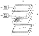
図1は、第1実施形態に係る画像表示装置10の模式図である。画像表示装置10は、2次元画像を表示可能な画像表示部11、偏光板12、屈折率分布型液晶光学素子としての液晶GRINレンズ20、第1電圧制御部50、及び第2電圧制御部51を備えている。画像表示部11は、画素がマトリクス状に配列された、所謂フラットパネルディスプレイ(FPD)が好ましく、そのような画像表示部として、非発光型の液晶ディスプレイ(LCD)、発光型のプラズマディスプレイ(PDP:Plasma Display Panel)、発光型の有機EL(electroluminescence)ディスプレイなどが用いられる。非発光型のディスプレイは、バックライトを有し、このバックライトからの光線を用いて画像を表示する。[First Embodiment]
FIG. 1 is a schematic diagram of an
図1の偏光板12に記載した矢印(第1方向D1)は、偏光方向を示している。偏光板12は、画像表示部11からの光線を偏光し、第1方向D1の直線偏光を射出する。図1では、偏光方向を説明するために、偏光板12を画像表示部11から抽出して示しているが、一般的には、画像表示部11と偏光板12とを合わせて画像表示部が構成される。液晶GRINレンズ20は、画像表示部11から画像が射出される側に配置されている。
An arrow (first direction D1) described on the
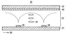
図2は、液晶GRINレンズ20の断面図である。液晶GRINレンズ20は、液晶層の両側に配置された2つの電極によって屈折率分布を作り出すレンズである。液晶GRINレンズ20は、一対の透明基板(例えばガラス基板)21及び22、透明基板21及び22に挟持された液晶層23、複数の第1電極30、及び第2電極40を備えている。
FIG. 2 is a cross-sectional view of the liquid
複数の第1電極30は、液晶層23側の透明基板21上に設けられている。図2の断面図には、2本の第1電極30のみを抽出して示している。第1電極30の具体的な構成については後述する。第2電極40は、液晶層23側の透明基板22上に平面状に設けられている。第2電極40の面積は、例えば、複数の第1電極30を包含する面積とほぼ同じに設定される。第1電極30及び第2電極40は、透明電極からなる。
The plurality of
液晶層23は、複数の液晶分子24を含んでいる。本実施形態では、液晶分子24は一軸性複屈折を示す物質が用いられる。液晶層23に電界を印加しない状態での液晶分子24の初期配向は、その長軸方向が第1方向D1になるように設定される。このような初期配向は、例えばラビング処理された配向膜(図示せず)によって制御される。
The
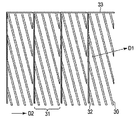
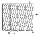
図3は、複数の第1電極30の平面図である。複数の第1電極30は、第1方向D1に沿って等間隔に配列されている。各第1電極30の幅は、第1電極30の配列ピッチの半分より小さく形成される。第1電極30の配列ピッチとは、第1方向D1において、第1電極30の幅と第1電極30間の距離とを足した長さである。複数の第1電極30は、第1方向と異なる第2方向D2に沿って配列する複数の第1電極領域31に分割されている。例えば、画像表示装置10を縦置きにした場合は、第2方向D2は、画面の水平方向に対応し、画像表示装置10を平置きにした場合は、第2方向D2は、画面の横方向に対応する。
FIG. 3 is a plan view of the plurality of
各第1電極領域31に含まれる所定数の第1電極30は、引出線32及び33によって電気的に接続されている。引出線32及び33は、第1電極30と同じ材料からなる。引出線32は、第2方向D2に直交する方向に延伸し、第2方向D2における第1電極領域31の端部に配置されている。引出線33は、引出線32に電気的に接続され、第1電極領域31の上端に配置され、第2方向D2に延伸している。引出線33は、第1電極領域31内において、引出線32によって電気的に接続されない第1電極30を電気的に接続している。このような構成を有する複数の第1電極30は、第1電極領域31を単位として電圧制御が可能となる。
A predetermined number of
液晶GRINレンズ20は、隣接する2つの第1電極30によって柱状の1個のレンズが形成される。隣接する2つの第1電極30間の距離(具体的には、隣接する2つの第1電極30それぞれの中心間の距離)がレンズピッチとなる。従って、液晶GRINレンズ20は、第2方向D2に直交する方向に対して傾いた斜めレンズが第1方向D1に複数個配列されたレンズアレイを構成している。液晶GRINレンズ20の傾き、すなわち第2方向D2と第1方向D1との成す角度θは、“θ≠0,−45°<θ<45°”の条件を満たす。
In the liquid
(動作)
次に、液晶GRINレンズ20の動作について説明する。液晶GRINレンズ20の電圧制御は、図1に示した第1電圧制御部50及び第2電圧制御部51によって行われる。第1電圧制御部50は、複数の引出線32(又は引出線33)のそれぞれに電気的に接続され、複数の引出線32をそれぞれ独立して電圧制御できるように構成されている。第2電圧制御部51は、第2電極40に電気的に接続され、第2電極40を電圧制御する。(Operation)
Next, the operation of the liquid
まず、3D表示を行う場合の液晶GRINレンズ20の動作について説明する。第2電圧制御部51は、第2電極40に基準電圧(例えば接地電圧)を印加する。第1電圧制御部50は、3D表示を行う領域に対応する第1電極領域31の引出線32に、基準電圧より高い所定の電圧V1を印加する。電圧V1は、閾値電圧Vth以上に設定される。Vthは、レンズ効果を発現するための閾値電圧であり、液晶層23に閾値電圧Vth以上の電位差を与えることで、長軸が水平方向の液晶分子24が垂直方向に立ち上がる。閾値電圧Vthは、第2電極40を接地電圧に固定して第1電極30の電圧を次第に大きくすることにより、実験的に求めることができる。
First, the operation of the liquid
前述したように、複数の引出線32はそれぞれ、複数の第1電極領域31に設けられ、各引出線32は、これに対応する第1電極領域31に含まれる所定数の第1電極30に電気的に接続されている。従って、ある引出線32に電圧V1が印加されると、該当する第1電極領域31に含まれる所定数の第1電極30にも、同じ電圧V1が印加されることになる。
As described above, the plurality of
図4は、液晶層23に電界を印加した場合の液晶ダイレクタ分布を示す図である。図4に示した符号24Aは、液晶分子24の長軸方向(長手方向)を示すダイレクタである。電圧V1が印加された第1電極30付近(レンズ端部)においては、印加された電圧の影響により、液晶分子24が立ち上がる。液晶分子24が立ち上がった液晶領域では、画像表示部11から射出された光線は、液晶ダイレクタと垂直に交わる割合が小さいため、複屈折の影響をほとんど受けない。このため、レンズ端部の屈折率が小さくなり、結果として光路長も小さくなる。
FIG. 4 is a diagram showing a liquid crystal director distribution when an electric field is applied to the
一方、第1電極30から離れる、すなわちレンズ中心に向かうにつれて、画像表示部11から射出された光線は、液晶ダイレクタと垂直に交わる割合が多くなるため、複屈折の影響を大きく受ける。このため、レンズ中心に向かうにつれて、徐々に屈折率が大きくなる。このように、隣接する2つの第1電極30間では、電界分布が徐々変化し、これにより屈折率分布及び光路長も徐々変化する。この結果、図2の破線で示すように、レンズとしての屈折率分布が実現されることになる。このように電圧V1が印加された第1電極領域31では、レンズの効果が発現する。
On the other hand, as the distance from the
そして、画像表示部11の画像は、液晶GRINレンズ20に含まれる複数のレンズによって光線方向が制御されるため、画像表示装置10は、複数の視差画像を表示することができる。これにより、観測者が立体画像を視認することが可能となる。このようにして、部分的に3D表示が実現される。
Since the light direction of the image on the
次に、2D表示を行う場合の液晶GRINレンズ20の動作について説明する。第2電圧制御部51は、第2電極40に基準電圧(例えば接地電圧)を印加する。第1電圧制御部50は、2D表示を行う領域に対応する第1電極領域31の引出線32に、第2電極40と同じ電圧、すなわち接地電圧を印加する。この場合、液晶層23には電界が印加されず、液晶分子24は初期配向を維持するため、レンズとしての屈折率分布は実現されない。この結果、接地電圧が印加された第1電極領域31では、レンズ効果が発現せず、部分的に2D表示が実現される。なお、2D表示を行う場合において、第1電極30に印加される電圧は、接地電圧に限らず、閾値電圧Vth未満であればよい。
Next, the operation of the liquid
(効果)
以上詳述したように第1実施形態では、液晶GRINレンズ20は、対向配置された一対の透明基板21及び22と、透明基板21及び22間に設けられた液晶層23と、液晶層23側の透明基板21上に設けられ、第1方向D1に沿って配列された複数の第1電極30と、液晶層23側の透明基板22上に設けられた第2電極40とを具備する。そして、複数の第1電極30は、第1方向D1と異なる第2方向D2に沿って配列された複数の第1電極領域31に分割される。また、各第1電極領域31に含まれる所定数の第1電極30は、引出線32によって電気的に接続されるようにしている。(effect)
As described in detail above, in the first embodiment, the liquid
従って第1実施形態は、以下の効果を有する。
第1電極領域31の境界(すなわち、引出線32のライン)は、レンズの境界(すなわち、第1電極30のライン)とは独立して設定される。そして、本実施形態では、第1電極領域31を単位として、レンズ機能のオン/オフを切り替えることが可能となる。これにより、第2方向D2に直交する方向に対して傾いた斜めレンズアレイを構成する液晶GRINレンズ20において、レンズの境界に束縛されることなく、矩形領域を単位として、部分的に2D表示と3D表示との切り替えを実現することができる。Therefore, the first embodiment has the following effects.
The boundary of the first electrode region 31 (that is, the line of the lead line 32) is set independently of the boundary of the lens (that is, the line of the first electrode 30). In the present embodiment, the lens function can be switched on / off in units of the
また、本実施形態では、画像表示部11の光線が射出される側に液晶GRINレンズ20を設けるだけで部分的に2D表示と3D表示との切り替えを実現することができる。すなわち、偏光切替セルが不要であるため、2D/3D表示切替が可能な画像表示装置10の低コスト化、薄型化が実現できる。
Further, in the present embodiment, switching between 2D display and 3D display can be partially realized only by providing the liquid
また、引出線32を第2方向D2における第1電極領域31の端部に設けているため、引出線32を配置したことに起因する画質の低下を抑制することができる。第1電極領域31の境界においては、第1電極30を分断した影響により、電界分布に若干の乱れが発生する場合がある。また、引出線32の近傍においては、やはり電界分布に若干の乱れが発生する場合がある。第1電極領域31間の距離、すなわち引出線32と第1電極30の分断された部分との距離を近づけることにより、電界分布の乱れが影響する領域を小さくすることができる。これにより、画像表示装置10の画質の低下を抑制することができる。
Moreover, since the
本実施形態では、レンズの境界に第1電極30を配置した最低限の構成を用いて液晶GRINレンズ20の中心概念を説明したが、本実施形態はこれに限定されるものではない。さらに多くの電極を用いてレンズとしての屈折率分布を形成することができる。
In the present embodiment, the central concept of the liquid
また、本実施形態における液晶層の初期配向は水平方向の水平配向であるものとして説明したが、液晶配向はこれに限定されるものではない。他の液晶モードも適用可能である。 In addition, although the initial alignment of the liquid crystal layer in the present embodiment has been described as horizontal alignment in the horizontal direction, the liquid crystal alignment is not limited to this. Other liquid crystal modes are also applicable.
また、本実施形態では、屈折率分布型液晶光学素子が液晶レンズアレイ素子として動作するものとして説明したが、本実施形態はこれに限定されるものではない。液晶光学素子は3D表示を実現するための性能を備えていればよく、例えば、完全なレンズとしての屈折率分布が実現されていなくてもよいし、プリズムアレイ素子として機能するものでもよい。 In the present embodiment, the gradient index liquid crystal optical element is described as operating as a liquid crystal lens array element, but the present embodiment is not limited to this. The liquid crystal optical element only needs to have performance for realizing 3D display. For example, the refractive index distribution as a complete lens may not be realized, or the liquid crystal optical element may function as a prism array element.
さらに、本実施形態では、屈折率分布型液晶光学素子について説明したが、使用される材料は液晶に限定されるものではない。同様に電気光学効果を有する材料であれば適用可能である。 Furthermore, in the present embodiment, the gradient index liquid crystal optical element has been described, but the material used is not limited to liquid crystal. Similarly, any material having an electro-optic effect is applicable.
[第2実施形態]
第2実施形態は、複数の第1電極30を電気的に接続する引出線32の他の構成例について示している。本実施形態の液晶光学素子である液晶GRINレンズ20においては、第1実施形態と比較して、引出線32の配置が異なる。図5は、第2実施形態に係る複数の第1電極30の平面図である。[Second Embodiment]
2nd Embodiment has shown about the other structural example of the
図5に示すように、各第1電極領域31において、隣接する2つの第1電極30間には、長さが最短となるように引出線32が配置され、この引出線32は、隣接する2つの第1電極30を電気的に接続している。換言すれば、引出線32は、隣接する2つの第1電極30間において、第1電極30の配列方向である第1方向D1に延伸している。各第1電極領域31に含まれる複数の引出線32は、第1実施形態と同様に、第2方向D2における第1電極領域31の端部に配置されている。これにより、各第1電極領域31に含まれる所定数の第1電極30は、複数の引出線32及び引出線33によって電気的に接続される。
As shown in FIG. 5, in each
また、本実施形態では、ラビング方向を第1方向D1としているため、ラビング方向と引出線32の延伸方向とが一致している。本実施形態におけるその他の構成、及び動作は、第1実施形態と同様である。
Moreover, in this embodiment, since the rubbing direction is the first direction D1, the rubbing direction and the extending direction of the
以上詳述したように本実施形態によれば、引出線32の長さを第1実施形態よりも短くすることができる。この結果、電圧印加時において、引出線32からの電界により液晶GRINレンズ20としての液晶配向分布が乱されるのを抑制することができる。これにより、画像表示装置10の画質が低下するのを抑制することができる。特に、本実施形態では、長さが最短となるように引出線32が配置されているため、画質が低下するのを抑制するという効果をより高めることができる。
As described above in detail, according to the present embodiment, the length of the
また、引出線32の延伸方向とラビング方向とを一致させているため、引出線32からの電界により液晶分子24がツイスト変形するのを抑制することができる。これにより、画像表示装置10の画質を向上させることができる。
In addition, since the extending direction of the
なお、本実施形態では、長さが最短となるように第1電極30間に引出線32が配置されているものとして説明したが、これに限定されるものではない。引出線32の長さが最短でない場合、すなわち、引出線32の延伸方向が第1方向D1に対して傾いている場合でも、画質の改善効果を得ることができる。
本実施形態におけるその他の効果は、第1実施形態と同様である。In the present embodiment, the
Other effects in the present embodiment are the same as those in the first embodiment.
[第3実施形態]
第3実施形態は、複数の第1電極30を電気的に接続する引出線32のさらに他の構成例について示している。本実施形態の液晶光学素子である液晶GRINレンズ20においては、第2実施形態と比較して、引出線32の配置が異なる。図6は、第3実施形態に係る複数の第1電極30の平面図である。[Third Embodiment]
3rd Embodiment has shown about the further another structural example of the
前述したように第2実施形態では、各第1電極領域31において、複数の引出線32は、第2方向D2に直交する方向に一列に配置されていた。これに対し、本実施形態では、図6に示すように、各第1電極領域31において、複数の引出線32は、千鳥状に配置されている。この結果、複数の引出線32は、特定の部位に集中して配置されることなく、分散して配置される。本実施形態におけるその他の構成、及び動作は、第1実施形態と同様である。
As described above, in the second embodiment, in each
以上詳述したように本実施形態によれば、引出線32に起因して液晶配向分布が乱される部分を、分散させることができる。これにより、本実施形態は、第2実施形態のように直線状に並べて周期的に配置する場合に比べて、液晶配向の乱れを目立ちにくくすることができる。これにより、画像表示装置10の画質の向上が可能となる。
本実施形態におけるその他の効果は、第2実施形態と同様である。As described above in detail, according to the present embodiment, the portion where the liquid crystal alignment distribution is disturbed due to the
Other effects in the present embodiment are the same as those in the second embodiment.
[第4実施形態]
第4実施形態は、透明基板22上に設けられる第2電極40を複数に分割して形成し、2D/3D表示を切り替える領域の単位を、第1実施形態に比べて小さく制御できるようにしている。図7は、第4実施形態に係る画像表示装置10の模式図である。図8は、液晶GRINレンズ20を構成する第1電極30及び第2電極40の平面図である。[Fourth Embodiment]
In the fourth embodiment, the
本実施形態の液晶GRINレンズ20は、第1実施形態と比較して、第2電極40の形状が異なる。第1実施形態においては、第2電極40は第2基板22上に平面状に形成されていた。これに対し、本実施形態では、第2電極40が複数に分割して形成され、この分割された複数の第2電極40は、第2方向D2に直交する第3方向D3に沿って配列されている。本実施形態におけるその他の構成は、第1実施形態と同様である。
The liquid
本実施形態では、第1電極30及び第2電極40にそれぞれ印加する電圧を選択することにより、第2方向D2のみならず、第3方向D3においても、部分的に2D/3D表示切替を実現することができる。
In this embodiment, 2D / 3D display switching is partially realized not only in the second direction D2 but also in the third direction D3 by selecting voltages to be applied to the
次に、液晶GRINレンズ20の動作について説明する。第2電圧制御部51は、複数の第2電極40のそれぞれに電気的に接続され、複数の第2電極40をそれぞれ独立して電圧制御できるように構成されている。第1電圧制御部50の構成は、第1実施形態と同じである。図8の構成例では、液晶GRINレンズ20は、4個の第1電極領域31、及び4個の第2電極40を備えているため、16(4×4)分割された表示領域で異なる電圧制御を行うことができる。
Next, the operation of the liquid
第1電極30の印加電圧をV1on、V1offとし、第2電極40の印加電圧をV2on、V2offとする。液晶GRINレンズ20のレンズ効果を発現させる表示領域に対応した第1電極30にはV1onを、第2電極40にはV2onを印加する。レンズ効果を発現させない表示領域に対応した第1電極30にはV1offを、第2電極40にはV2offを印加する。Vthは、レンズ効果を発現するための閾値電圧である。これらの印加電圧を次式が成立するように選定する。
The applied voltages of the
|V1on−V2on|≧Vth
|V1on−V2off|<Vth
|V1off−V2on|<Vth
|V1off−V2off|<Vth
図9は、部分的に3D表示させるための電圧関係の一例を示す図である。一例として、図9の破線で示した領域、すなわち中央の4つの分割領域のみを3D表示にする場合について説明する。この例の場合、第1電圧制御部50は、第1電極30−2及び30−3にそれぞれ電圧V1onを印加し、それ以外の第1電極30−1及び30−4にそれぞれ電圧V1offを印加する。また、第2電圧制御部51は、第2電極40−2及び40−3にそれぞれ電圧V2onを印加し、それ以外の第2電極40−1及び40−4にそれぞれ電圧V2offを印加する。このような電圧制御により、図9の破線で示した領域のみに対して閾値電圧Vth以上の電位差が与えられ、この領域にレンズ効果が発現する。これにより、図9の破線で示した領域が3D表示される。| V1on-V2on | ≧ Vth
| V1on-V2off | <Vth
| V1off-V2on | <Vth
| V1off−V2off | <Vth
FIG. 9 is a diagram illustrating an example of a voltage relationship for partial 3D display. As an example, a case will be described in which only the region indicated by the broken line in FIG. In this example, the first
一方、図9の破線で示した領域以外では、閾値電圧Vth以上の電位差が与えられないので、この領域にレンズ効果は発現しない。これにより、図9の破線で示した領域以外が2D表示される。 On the other hand, since a potential difference equal to or higher than the threshold voltage Vth is not provided outside the region indicated by the broken line in FIG. 9, no lens effect appears in this region. Thereby, the area other than the area indicated by the broken line in FIG. 9 is displayed in 2D.
このように、本実施形態によれば、第1電極30にV1onが、第2電極40にV2onが印加された領域ではレンズが有効になり、それ以外の領域ではレンズ効果が発現されない。これにより、画面の縦横方向のどちらにおいても、部分的に2D表示と3D表示との切り替えを実現することができる。
本実施形態におけるその他の効果は、第1実施形態と同様である。また、第4実施形態に、第2及び第3実施形態を適用することも可能であることは勿論である。Thus, according to the present embodiment, the lens is effective in the region where V1on is applied to the
Other effects in the present embodiment are the same as those in the first embodiment. Of course, the second and third embodiments can be applied to the fourth embodiment.
[第5実施形態]
第5実施形態は、液晶レンズアレイに代えて、視差発生手段として液晶パララックスバリア(視差バリア)を用いて2D/3D表示切替が可能な画像表示装置10を構成している。液晶パララックスバリアは、一方向に配列されたスリットアレイを有する。画像表示部11からの光線は、液晶パララックスバリアのスリット(開口部)越しに観測されることになるため、画像表示部11の画素の観測可能な方向は、ごく狭い範囲に限られる。スリットのピッチ及びスリットと画像表示部11との距離を適正に設定することにより、画像表示装置10は、複数の視差画像を表示することができる。これにより、観測者が立体画像を視認することが可能となる。[Fifth Embodiment]
In the fifth embodiment, instead of the liquid crystal lens array, an
図10は、第5実施形態に係る画像表示装置10の模式図である。画像表示装置10は、画像表示部11、偏光板12、液晶光学素子としての液晶パララックスバリア20、及び偏光板13を備えている。
FIG. 10 is a schematic diagram of an
図10の偏光板13に記載した矢印は、偏光方向を示している。偏光板13は、第4方向D4(第2方向D2と直交する方向)の直線偏光を射出する。すなわち、偏光板13の偏光方向は、偏光板12の偏光方向に対して90°の角度を成している。
The arrow described in the
図11は、液晶パララックスバリア20の断面図である。液晶層23は、これに含まれる液晶分子24が透明基板21に水平に並んでおり、かつ透明基板21と透明基板22との間で90°ねじれている、いわゆるTN(Twisted Nematic)型液晶層である。これにより、電界が印加されない状態では、偏光板12により直線偏光された光線は、その偏光方向(偏光面)が液晶分子24に沿ってTN型液晶層23内を90°回転し、偏光板12に対して90°の偏光方向を持つ偏光板13を透過して白状態の表示となる。すなわち、液晶パララックスバリア20は、TNモード、かつ、ノーマリホワイト方式(電界が印加されていない状態で白表示となる)である。TN型液晶層23の初期配向は、互いに直交する方向にラビング処理された2つの配向膜(図示せず)で液晶分子24を挟むことで実現される。液晶層23の厚さは、液晶材料に応じて、TNモードが実現できる最適な値に設定される。
FIG. 11 is a cross-sectional view of the liquid
図12は、複数の第1電極30の平面図である。複数の第1電極30は、第1方向D1に沿って等間隔に配列されている。各第1電極30の幅は、第1電極30の配列ピッチの半分より大きく形成される。この結果、パララックスバリアのスリットとして機能する、第1電極30間の開口部が、第1電極30の配列ピッチの半分未満となる。複数の第1電極30は、第2方向D2に沿って配列する複数の第1電極領域31に分割されている。引出線32及び33の構成は、第1実施形態と同じである。
FIG. 12 is a plan view of the plurality of
次に、液晶パララックスバリア20の動作について説明する。まず、3D表示を行う場合の液晶パララックスバリア20の動作について説明する。
Next, the operation of the liquid
第2電圧制御部51は、第2電極40に基準電圧(例えば接地電圧)を印加する。第1電圧制御部50は、3D表示を行う領域に対応する第1電極領域31の引出線32に、基準電圧より高い所定の電圧V1を印加する。電圧V1は、閾値電圧Vth以上に設定される。これにより、第1電極30と第2電極40とに挟まれた液晶領域には電界が印加され、液晶分子24が立ち上がる。液晶分子24が立ち上がった領域では、偏光板12から射出された光線は、その偏光方向が90°回転せず、偏光板13によって遮断されて黒表示となる。すなわち、第1電極30と第2電極40とに挟まれた液晶領域は、光線を遮断するバリアとして機能する。
The second
一方、第1電極30と第2電極40とに挟まれていない液晶領域、すなわち、第1電極30が形成されていない領域(スリット)では、液晶分子24に電界が印加されず、この液晶分子24は、初期配向を維持する。これにより、スリットでは、偏光板12から射出された光線は、その偏光方向が90°回転し、偏光板13を透過する。この結果、スリットによって、部分的に3D表示が実現される。
On the other hand, in the liquid crystal region that is not sandwiched between the
次に、2D表示を行う場合の液晶パララックスバリア20の動作について説明する。第2電圧制御部51は、第2電極40に基準電圧(例えば接地電圧)を印加する。第1電圧制御部50は、2D表示を行う領域に対応する第1電極領域31の引出線32に、第2電極40と同じ電圧、すなわち接地電圧を印加する。この場合、液晶層23には電界が印加されないので、液晶分子24は初期配向を維持する。これにより、接地電圧が印加された第1電極領域31では、偏光板12から射出された光線は、その偏光方向が90°回転し、偏光板13を透過する。この結果、電界が印加されていない液晶領域では、スリットが形成されず、2D表示が実現されることになる。なお、2D表示を行う場合において、第1電極30に印加される電圧は、接地電圧に限らず、閾値電圧Vth未満であればよい。
Next, the operation of the liquid
以上詳述したように本実施形態によれば、第1電極領域31の境界(すなわち、引出線32のライン)は、スリットの境界(すなわち、第1電極30のライン)とは独立して設定される。そして、本実施形態では、第1電極領域31を単位として、スリット機能のオン/オフを切り替えることが可能となる。これにより、第2方向D2に直交する方向に対して傾いたスリットを有する液晶パララックスバリア20において、スリットの境界に束縛されることなく、矩形領域を単位として、部分的に2D表示と3D表示との切り替えを実現することができる。
As described above in detail, according to the present embodiment, the boundary of the first electrode region 31 (that is, the line of the lead line 32) is set independently of the boundary of the slit (that is, the line of the first electrode 30). Is done. In this embodiment, the slit function can be switched on / off in units of the
また、第1電極30の幅を第1電極30の配列ピッチの半分よりも大きく形成することで、パララックスバリアの遮光効果を有効に発揮させることができる。本実施形態におけるその他の効果は、第1実施形態と同様である。
Further, by forming the width of the
[第6実施形態]
前述の第4実施形態においては、透明基板21側に形成されている電極は第1電極30のみであった。しかし実際に液晶GRINレンズを形成する場合には、実現するレンズの焦点距離などの条件によっては、レンズ性能向上のために電極を追加した方が好ましい場合がある。そこで第6実施形態では、レンズ端部に第1電極30を配置し、レンズ中央部に第1電極30と異なる電圧制御が行える第3電極60を配置することで、レンズ性能をより向上させるようにしている。[Sixth Embodiment]
In the fourth embodiment described above, the
図13は、第6実施形態に係る画像表示装置10の模式図である。図14は、液晶GRINレンズ20の断面図である。液晶GRINレンズ20は、一対の透明基板21及び22、透明基板21及び22間に設けられた誘電体層25、透明基板21及び誘電体層25に挟持された液晶層23、複数の第1電極30、複数の第2電極40、複数の第3電極60、第1電圧制御部50、第2電圧制御部51、及び第3電圧制御部52を備えている。
FIG. 13 is a schematic diagram of the
複数の第3電極60は、液晶層23側の透明基板21上に設けられている。複数の第1電極30は、液晶層23側の誘電体層25上に設けられている。複数の第2電極40は、液晶層23側の透明基板22上に設けられている。第1電極30、第2電極40、及び第3電極60は、透明電極からなる。誘電体層25は、第1電極30と第3電極60とが導通しないようにするための絶縁層からなる。
The plurality of
図15は、第1電極30、第2電極40及び第3電極60の平面図である。第1電極30及び第2電極40の平面形状は、第4実施形態と同じである。
複数の第3電極60は、第1電極30と同様に、第1方向D1に沿って等間隔に配列されている。第3電極60の配列ピッチは、第1電極30と同じであり、各第3電極60は、第1電極30間に配置されている。第3電極60の幅は、第1電極30間の距離より小さく形成される。液晶GRINレンズ20は、隣接する2つの第1電極30によって柱状の1個のレンズが形成される。よって、隣接する2つの第1電極30がレンズの両端に配置されて端部電極を構成し、隣接する2つの第1電極30間の第3電極60がレンズの中心に配置されて中心電極を構成する。FIG. 15 is a plan view of the
The plurality of
複数の第3電極60は、第3方向D3に沿って配列する複数の第3電極領域61に分割されている。各第3電極領域61に含まれる所定数の第3電極60は、引出線62によって電気的に接続されている。引出線62は、第3電極と同じ材料からなる。引出線62は、第3方向D3に延伸し、第3方向D3における第3電極領域61の端部に配置されている。第3電極領域61は、第2電極40に対応して配置されており、第3電極領域61のサイズは、第2電極40のサイズとほぼ同じである。本実施形態におけるその他の構成は、第4実施形態と同じである。
The plurality of
次に、液晶GRINレンズ20の動作について説明する。第3電圧制御部52は、複数の引出線62のそれぞれに電気的に接続され、複数の引出線62をそれぞれ独立して電圧制御できるように構成されている。
Next, the operation of the liquid
第3電圧制御部52は、3D表示を行う領域に対応する引出線62を駆動する。この時、第3電圧制御部52は、引出線62を介して第3電極60に、第2電極40と同じ電圧を印加する。第1電圧制御部50及び第2電圧制御部51の動作は、第4実施形態と同じである。
The third
本実施形態では、第1電極30がレンズ端部に位置し、第3電極60がレンズ中央部に位置している。第1電極30及び第2電極40間の液晶領域には閾値電圧Vth以上の電位差が与えられ、一方、第3電極60及び第2電極40間の液晶領域には閾値電圧Vth以上の電位差が与えられない。これにより、レンズ端部では、液晶分子が基板に対して立ち上がるため、屈折率を小さくすることができる。また、第3電極60が位置するレンズ中央部では、電位差がほぼ0Vに設定されるため、レンズ中央部の液晶領域には不要な電界が印加されない。このため、隣接する2つの第1電極30間では、電界が徐々変化する理想的な電界分布が得られ、よりレンズとして好ましい屈折率分布を実現することが可能となる。
In this embodiment, the
一方、2D表示を行う場合は、第1電圧制御部50、第2電圧制御部51及び第3電圧制御部52はそれぞれ、第1電極30、第2電極40及び第3電極60に基準電圧(例えば接地電圧)を印加する。この場合、液晶層23には電界が印加されないので、液晶分子24は初期配向を維持する。このため、レンズとしての屈折率分布は実現さず、2D表示が実現されることになる。
On the other hand, when 2D display is performed, the first
以上詳述したように本実施形態によれば、第4実施形態と同様に、画面の縦横方向のどちらにおいても、部分的に2D表示と3D表示との切り替えを実現することができる。また、1個のレンズとして機能する第1電極30間の液晶領域において、電界分布を制御するための第3電極60を追加しているため、より理想的な電界分布を得ることが可能となり、ひいては、よりレンズとして好ましい屈折率分布を実現することが可能となる。本実施形態におけるその他の効果は、第1実施形態と同様である。
As described above in detail, according to the present embodiment, similarly to the fourth embodiment, switching between 2D display and 3D display can be partially realized in both the vertical and horizontal directions of the screen. In addition, since the
なお、本実施形態においては、1種類の電極(第3電極60)を追加した場合について説明したが、これに限定されない。さらに多くの電極を用いることで、電界分布をより細かく制御することも可能である。 In addition, in this embodiment, although the case where one kind of electrode (3rd electrode 60) was added was demonstrated, it is not limited to this. Further, the electric field distribution can be controlled more finely by using more electrodes.
また、第1実施形態と同様に、第2電極40は、透明基板22上に平面状に形成されていてもよい。この場合、複数の第3電極60は、複数の領域に分割する必要はなく、複数の第3電極60を纏めて1本の引出線62で電気的に接続すればよい。
Further, similarly to the first embodiment, the
本発明のいくつかの実施形態を説明したが、これらの実施形態は、例として提示したものであり、発明の範囲を限定することは意図していない。これら新規な実施形態は、その他の様々な形態で実施されることが可能であり、発明の要旨を逸脱しない範囲で、種々の省略、置き換え、変更を行うことができる。これら実施形態やその変形は、発明の範囲や要旨に含まれるとともに、特許請求の範囲に記載された発明とその均等の範囲に含まれる。 Although several embodiments of the present invention have been described, these embodiments are presented by way of example and are not intended to limit the scope of the invention. These novel embodiments can be implemented in various other forms, and various omissions, replacements, and changes can be made without departing from the scope of the invention. These embodiments and modifications thereof are included in the scope and gist of the invention, and are included in the invention described in the claims and the equivalents thereof.
10…画像表示装置、11…画像表示部、12,13…偏光板、20…液晶光学素子(液晶GRINレンズ、液晶パララックスバリア)、21,22…透明基板、23…液晶層、24…液晶分子、25…誘電体層、30…第1電極、31…第1電極領域、32,33…引出線、40…第2電極、50〜52…電圧制御部、60…第3電極、61…第3電極領域、62…引出線。
DESCRIPTION OF
Claims (9)
前記第1基板の前記主面に対向配置された第2基板と、
前記第1及び第2基板間に設けられた液晶層と、
前記第1領域及び前記第2領域の各々に設けられ、前記境界線と交差する第1方向に延在しかつ前記第1方向と交差する第2方向に並ぶ複数の第1電極と、
前記各領域における複数の第1電極に電気的に接続され、前記境界線付近において前記境界線に沿って設けられた第1引出線と、
前記液晶層側の前記第2基板上に設けられ、前記第1領域と前記第2領域とに対向して形成された複数の第2電極と、
を具備し、
前記第1領域及び前記第2領域は、前記境界線と交差する第3方向に並び、
前記第1方向は、前記第3方向及び前記境界線と交差することを特徴とする液晶光学素子。 A first substrate having a main surface having a first region and a second region in contact with the first region via a boundary line;
A second substrate disposed opposite to the main surface of the first substrate;
A liquid crystal layer provided between the first and second substrates;
A plurality of first electrodes provided in each of the first region and the second region, extending in a first direction intersecting the boundary line and arranged in a second direction intersecting the first direction;
A first lead line electrically connected to the plurality of first electrodes in each of the regions, and provided along the boundary line in the vicinity of the boundary line;
A plurality of second electrodes provided on the second substrate on the liquid crystal layer side and formed to face the first region and the second region ;
Equipped with,
The first region and the second region are arranged in a third direction intersecting the boundary line,
The liquid crystal optical element , wherein the first direction intersects the third direction and the boundary line .
前記第1領域と前記第2領域とは、交互に配列されることを特徴とする請求項1に記載の液晶光学素子。 A second lead line electrically connected to the first electrode and the first lead line and extending in the third direction ;
The liquid crystal optical element according to claim 1, wherein the first region and the second region are alternately arranged .
前記第2電極に第2電圧を印加する第2電圧制御部と、
をさらに具備し、
前記第1電圧は、前記第2電圧に前記液晶層の閾値電圧を足した電圧以上であることを特徴とする請求項1に記載の液晶光学素子。 A first voltage controller for applying a first voltage to the first electrode;
A second voltage controller for applying a second voltage to the second electrode;
Further comprising
The liquid crystal optical element according to claim 1, wherein the first voltage is equal to or higher than a voltage obtained by adding a threshold voltage of the liquid crystal layer to the second voltage.
前記第1基板の前記主面に対向配置された第2基板と、
前記第1基板の前記主面上に設けられた誘電体層と、
前記誘電体層及び前記第2基板間に設けられた液晶層と、
前記誘電体層上かつ前記第1領域及び前記第2領域の各々に設けられ、前記境界線と交差する第1方向に延在しかつ前記第1方向と交差する第2方向に並ぶ複数の第1電極と、
前記各領域における複数の第1電極に電気的に接続され、前記境界線付近において前記境界線に沿って設けられた第1引出線と、
前記液晶層側の前記第2基板上に設けられ、前記第1領域と前記第2領域とに対向して形成された複数の第2電極と、
前記第1基板の前記主面上に設けられ、前記第1方向に延在しかつ前記第2方向に並び、前記複数の第1電極間に配置された複数の第3電極と、
を具備し、
前記第1領域及び前記第2領域は、前記境界線と交差する第3方向に並び、
前記第1方向は、前記第3方向及び前記境界線と交差することを特徴とする液晶光学素子。 A first substrate having a main surface having a first region and a second region in contact with the first region via a boundary line;
A second substrate disposed opposite to the main surface of the first substrate;
A dielectric layer provided on the main surface of the first substrate;
A liquid crystal layer provided between the dielectric layer and the second substrate;
A plurality of first layers provided on the dielectric layer and in each of the first region and the second region, extending in a first direction intersecting the boundary line and arranged in a second direction intersecting the first direction. One electrode;
A first lead line electrically connected to the plurality of first electrodes in each of the regions, and provided along the boundary line in the vicinity of the boundary line;
A plurality of second electrodes provided on the second substrate on the liquid crystal layer side and formed to face the first region and the second region ;
A plurality of third electrodes provided on the main surface of the first substrate, extending in the first direction and arranged in the second direction, and disposed between the plurality of first electrodes;
Equipped with,
The first region and the second region are arranged in a third direction intersecting the boundary line,
The liquid crystal optical element , wherein the first direction intersects the third direction and the boundary line .
前記第1領域と前記第2領域とは、交互に配列されることを特徴とする請求項5に記載の液晶光学素子。 A second lead line electrically connected to the first electrode and the first lead line and extending in the third direction ;
The liquid crystal optical element according to claim 5 , wherein the first region and the second region are alternately arranged .
前記複数の電極領域の各々に含まれる第3電極は、第3引出線に電気的に接続されることを特徴とする請求項5に記載の液晶光学素子。 The plurality of third electrodes are divided into a plurality of electrode regions provided corresponding to the plurality of second electrodes ,
The liquid crystal optical element according to claim 5 , wherein the third electrode included in each of the plurality of electrode regions is electrically connected to a third lead line.
前記第2電極及び前記第3電極に第2電圧を印加する第2電圧制御部と、
をさらに具備し、
前記第1電圧は、前記第2電圧に前記液晶層の閾値電圧を足した電圧以上であることを特徴とする請求項5に記載の液晶光学素子。 A first voltage controller for applying a first voltage to the first electrode;
A second voltage controller for applying a second voltage to the second electrode and the third electrode;
Further comprising
6. The liquid crystal optical element according to claim 5 , wherein the first voltage is equal to or higher than a voltage obtained by adding a threshold voltage of the liquid crystal layer to the second voltage.
Applications Claiming Priority (1)
| Application Number | Priority Date | Filing Date | Title |
|---|---|---|---|
| PCT/JP2011/067366 WO2013014802A1 (en) | 2011-07-28 | 2011-07-28 | Liquid crystal optical element and image display device |
Publications (2)
| Publication Number | Publication Date |
|---|---|
| JPWO2013014802A1 JPWO2013014802A1 (en) | 2015-02-23 |
| JP5774701B2 true JP5774701B2 (en) | 2015-09-09 |
Family
ID=47600685
Family Applications (1)
| Application Number | Title | Priority Date | Filing Date |
|---|---|---|---|
| JP2013525528A Expired - Fee Related JP5774701B2 (en) | 2011-07-28 | 2011-07-28 | Liquid crystal optical element and image display device |
Country Status (5)
| Country | Link |
|---|---|
| US (1) | US9279991B2 (en) |
| JP (1) | JP5774701B2 (en) |
| CN (1) | CN103597401A (en) |
| TW (1) | TWI479243B (en) |
| WO (1) | WO2013014802A1 (en) |
Families Citing this family (6)
| Publication number | Priority date | Publication date | Assignee | Title |
|---|---|---|---|---|
| JP6132281B2 (en) * | 2013-01-07 | 2017-05-24 | Nltテクノロジー株式会社 | Liquid crystal lens element, display device and terminal |
| TWI502247B (en) * | 2013-02-26 | 2015-10-01 | Chunghwa Picture Tubes Ltd | Autostereoscopic display device and display method thereof |
| JP6130727B2 (en) * | 2013-05-16 | 2017-05-17 | 株式会社東芝 | Liquid crystal optical device and image display device |
| TWI575255B (en) * | 2014-07-18 | 2017-03-21 | 深圳超多維光電子有限公司 | Liquid crystal lens and stereoscopic display |
| KR20160062311A (en) * | 2014-11-24 | 2016-06-02 | 삼성디스플레이 주식회사 | Liquid crystal lens unit and 3d display device |
| CN109790459B (en) | 2016-11-23 | 2022-08-12 | 广州华睿光电材料有限公司 | Organic compounds |
Family Cites Families (16)
| Publication number | Priority date | Publication date | Assignee | Title |
|---|---|---|---|---|
| GB9715397D0 (en) | 1997-07-23 | 1997-09-24 | Philips Electronics Nv | Lenticular screen adaptor |
| JP2000102038A (en) * | 1998-09-18 | 2000-04-07 | Sanyo Electric Co Ltd | Two-dimensional video image and three-dimensional video image compatible type video display device |
| US7163828B2 (en) * | 2003-03-24 | 2007-01-16 | Seiko Epson Corporation | Electrode, method of manufacturing the same, ferroelectric memory, and semiconductor device |
| US8094771B2 (en) | 2003-11-21 | 2012-01-10 | Global Technologies, Inc. | Nuclear voltaic cell |
| JP2005258013A (en) * | 2004-03-11 | 2005-09-22 | Sharp Corp | Display panel and display device |
| KR101087568B1 (en) * | 2004-12-30 | 2011-11-28 | 엘지디스플레이 주식회사 | parallax barrier liquid crystal display panel for stereoscopic 3-D display apparatus and manufacturing method the same |
| KR101113066B1 (en) * | 2005-05-26 | 2012-02-15 | 엘지디스플레이 주식회사 | stereoscopic 3 dimension display apparatus and parallax barrier liquid crystal display panel |
| TWI282004B (en) * | 2005-07-01 | 2007-06-01 | Chunghwa Picture Tubes Ltd | Liquid crystal display panel and liquid crystal display device |
| TW200809353A (en) * | 2006-07-07 | 2008-02-16 | Hitachi Displays Ltd | Optically isotropic liquid crystal materials and display apparatus using the same |
| KR100846707B1 (en) * | 2007-02-27 | 2008-07-16 | 삼성에스디아이 주식회사 | Electronic imaging device |
| EP2140304B1 (en) * | 2007-04-17 | 2011-08-31 | Koninklijke Philips Electronics N.V. | Beam-shaping device |
| JP2010224191A (en) | 2009-03-23 | 2010-10-07 | Toshiba Corp | Apparatus for displaying stereoscopic image |
| JP5521380B2 (en) * | 2009-04-13 | 2014-06-11 | ソニー株式会社 | 3D display device |
| TWI391738B (en) * | 2010-01-08 | 2013-04-01 | Unique Instr Co Ltd | A device for multifunctional liquid crystal parallax gratings |
| TWI439730B (en) * | 2010-07-16 | 2014-06-01 | Au Optronics Corp | Parallax barrier and application thereof |
| TW201217833A (en) * | 2010-10-27 | 2012-05-01 | Chunghwa Picture Tubes Ltd | Parallax barrier, method of adjusting parallax barrier transmittance and 3D display |
-
2011
- 2011-07-28 JP JP2013525528A patent/JP5774701B2/en not_active Expired - Fee Related
- 2011-07-28 CN CN201180071559.8A patent/CN103597401A/en active Pending
- 2011-07-28 WO PCT/JP2011/067366 patent/WO2013014802A1/en active Application Filing
- 2011-12-07 TW TW100145042A patent/TWI479243B/en active
-
2014
- 2014-01-27 US US14/164,589 patent/US9279991B2/en not_active Expired - Fee Related
Also Published As
| Publication number | Publication date |
|---|---|
| US9279991B2 (en) | 2016-03-08 |
| US20140139766A1 (en) | 2014-05-22 |
| TW201305696A (en) | 2013-02-01 |
| TWI479243B (en) | 2015-04-01 |
| WO2013014802A1 (en) | 2013-01-31 |
| CN103597401A (en) | 2014-02-19 |
| JPWO2013014802A1 (en) | 2015-02-23 |
Similar Documents
| Publication | Publication Date | Title |
|---|---|---|
| JP5329231B2 (en) | Autostereoscopic display device | |
| US9488842B2 (en) | Liquid crystal optical device and stereoscopic image display device | |
| JP4650279B2 (en) | Electro-optical device and electronic apparatus | |
| US9726898B2 (en) | Autostereoscopic display device | |
| JP5774701B2 (en) | Liquid crystal optical element and image display device | |
| JP2010224191A (en) | Apparatus for displaying stereoscopic image | |
| KR101852121B1 (en) | Display device | |
| JP2012141575A (en) | Image display device using diffractive element | |
| KR20120047534A (en) | Optical unit and display device having the same | |
| KR20130048070A (en) | Display apparatus | |
| KR20150142891A (en) | 3d display apparatus | |
| KR20080084527A (en) | Liquid crystal display device including liquid crystal lens | |
| TWI467245B (en) | Display apparatus and liquid crystal lens | |
| US20130222716A1 (en) | Liquid crystal optical element and stereoscopic image display device | |
| KR102061234B1 (en) | Display device and liquid crystal lends panel for the same | |
| US9658483B2 (en) | Liquid crystal lens and display including the same | |
| KR100879298B1 (en) | Electronic display device | |
| US9575326B2 (en) | Stereoscopic image display apparatus | |
| JP5781170B2 (en) | Optical device, image display device, driving device, and driving method | |
| JP2013174695A (en) | Liquid crystal lens and display device | |
| US20130265510A1 (en) | Three-dimensional display device and active optical element thereof | |
| KR20140060835A (en) | Switchable 3 dimensional stereography image display device | |
| US9256074B2 (en) | Liquid crystal optical element and stereoscopic image display device | |
| JP2012226216A (en) | Liquid crystal display device | |
| KR20130113813A (en) | 3 dimensional stereography image displayable device |
Legal Events
| Date | Code | Title | Description |
|---|---|---|---|
| A131 | Notification of reasons for refusal |
Free format text: JAPANESE INTERMEDIATE CODE: A131 Effective date: 20141118 |
|
| A521 | Request for written amendment filed |
Free format text: JAPANESE INTERMEDIATE CODE: A523 Effective date: 20150115 |
|
| A02 | Decision of refusal |
Free format text: JAPANESE INTERMEDIATE CODE: A02 Effective date: 20150310 |
|
| A521 | Request for written amendment filed |
Free format text: JAPANESE INTERMEDIATE CODE: A523 Effective date: 20150430 |
|
| A911 | Transfer to examiner for re-examination before appeal (zenchi) |
Free format text: JAPANESE INTERMEDIATE CODE: A911 Effective date: 20150511 |
|
| TRDD | Decision of grant or rejection written | ||
| A01 | Written decision to grant a patent or to grant a registration (utility model) |
Free format text: JAPANESE INTERMEDIATE CODE: A01 Effective date: 20150602 |
|
| A61 | First payment of annual fees (during grant procedure) |
Free format text: JAPANESE INTERMEDIATE CODE: A61 Effective date: 20150701 |
|
| R151 | Written notification of patent or utility model registration |
Ref document number: 5774701 Country of ref document: JP Free format text: JAPANESE INTERMEDIATE CODE: R151 |
|
| LAPS | Cancellation because of no payment of annual fees |