JP5771429B2 - Switching power supply - Google Patents
Switching power supply Download PDFInfo
- Publication number
- JP5771429B2 JP5771429B2 JP2011081485A JP2011081485A JP5771429B2 JP 5771429 B2 JP5771429 B2 JP 5771429B2 JP 2011081485 A JP2011081485 A JP 2011081485A JP 2011081485 A JP2011081485 A JP 2011081485A JP 5771429 B2 JP5771429 B2 JP 5771429B2
- Authority
- JP
- Japan
- Prior art keywords
- transistor
- power supply
- terminal
- resistor
- voltage
- Prior art date
- Legal status (The legal status is an assumption and is not a legal conclusion. Google has not performed a legal analysis and makes no representation as to the accuracy of the status listed.)
- Active
Links
Images


Classifications
-
- H—ELECTRICITY
- H02—GENERATION; CONVERSION OR DISTRIBUTION OF ELECTRIC POWER
- H02M—APPARATUS FOR CONVERSION BETWEEN AC AND AC, BETWEEN AC AND DC, OR BETWEEN DC AND DC, AND FOR USE WITH MAINS OR SIMILAR POWER SUPPLY SYSTEMS; CONVERSION OF DC OR AC INPUT POWER INTO SURGE OUTPUT POWER; CONTROL OR REGULATION THEREOF
- H02M3/00—Conversion of dc power input into dc power output
- H02M3/02—Conversion of dc power input into dc power output without intermediate conversion into ac
- H02M3/04—Conversion of dc power input into dc power output without intermediate conversion into ac by static converters
- H02M3/10—Conversion of dc power input into dc power output without intermediate conversion into ac by static converters using discharge tubes with control electrode or semiconductor devices with control electrode
- H02M3/145—Conversion of dc power input into dc power output without intermediate conversion into ac by static converters using discharge tubes with control electrode or semiconductor devices with control electrode using devices of a triode or transistor type requiring continuous application of a control signal
- H02M3/155—Conversion of dc power input into dc power output without intermediate conversion into ac by static converters using discharge tubes with control electrode or semiconductor devices with control electrode using devices of a triode or transistor type requiring continuous application of a control signal using semiconductor devices only
- H02M3/156—Conversion of dc power input into dc power output without intermediate conversion into ac by static converters using discharge tubes with control electrode or semiconductor devices with control electrode using devices of a triode or transistor type requiring continuous application of a control signal using semiconductor devices only with automatic control of output voltage or current, e.g. switching regulators
-
- H—ELECTRICITY
- H02—GENERATION; CONVERSION OR DISTRIBUTION OF ELECTRIC POWER
- H02M—APPARATUS FOR CONVERSION BETWEEN AC AND AC, BETWEEN AC AND DC, OR BETWEEN DC AND DC, AND FOR USE WITH MAINS OR SIMILAR POWER SUPPLY SYSTEMS; CONVERSION OF DC OR AC INPUT POWER INTO SURGE OUTPUT POWER; CONTROL OR REGULATION THEREOF
- H02M1/00—Details of apparatus for conversion
- H02M1/0003—Details of control, feedback or regulation circuits
- H02M1/0025—Arrangements for modifying reference values, feedback values or error values in the control loop of a converter
Landscapes
- Engineering & Computer Science (AREA)
- Power Engineering (AREA)
- Dc-Dc Converters (AREA)
Description
本発明は、非線形制御方式のスイッチング電源装置に関するものである。 The present invention relates to a non-linear control type switching power supply device.
図12A〜図12Cは、いずれも、非線形制御方式を採用したスイッチング電源装置の従来例を示す回路ブロック図及び動作波形図であり、図12Aではヒステリシス・ウィンドウ方式、図12Bではボトム検出オン時間固定方式、そして、図12Cではアッパー検出オフ時間固定方式を採用したスイッチング電源装置がそれぞれ描写されている。なお、図12A〜図12Cに各々描写されているスイッチング電源装置は、いずれも、入力電圧INを降圧して所望の出力電圧OUTを生成する降圧型DC/DCコンバータである。 12A to 12C are a circuit block diagram and an operation waveform diagram showing a conventional example of a switching power supply device adopting a non-linear control method, in which a hysteresis window method is shown in FIG. 12A and a bottom detection ON time is fixed in FIG. 12B. In FIG. 12C and FIG. 12C, switching power supply devices employing the upper detection off-time fixed method are respectively depicted. 12A to 12C are all step-down DC / DC converters that step down the input voltage IN and generate a desired output voltage OUT.
非線形制御方式のスイッチング電源装置は、線形制御方式(例えば電圧モード制御方式や電流モード制御方式)のスイッチング電源装置に比べて、簡単な回路構成で、高い負荷応答特性を得られるという特長を有している。 Nonlinear control switching power supply devices have the advantage that high load response characteristics can be obtained with a simple circuit configuration compared to switching power supply devices of linear control methods (for example, voltage mode control method and current mode control method). ing.
一方、非線形制御方式のスイッチング電源装置は、出力リップル電圧(=出力電圧OUTのリップル成分)を利用してコンパレータを駆動することにより、出力トランジスタのスイッチング制御を行うという構成上、出力リップル電圧を正しく検出するために、ある程度大きな振幅(波高値)の出力リップル電圧が必要であった。そのため、従来では、等価直列抵抗(ESR[Equivalent Series Resistance])が比較的大きい出力コンデンサ(例えば導電性高分子タイプ)を用いなければならず、部品選定の制約やコストアップが招かれていた。 On the other hand, the switching power supply device of the non-linear control method uses the output ripple voltage (= ripple component of the output voltage OUT) to drive the comparator, thereby controlling the switching of the output transistor. In order to detect, an output ripple voltage having a certain large amplitude (peak value) was required. For this reason, conventionally, an output capacitor (for example, a conductive polymer type) having a relatively large equivalent series resistance (ESR [Equivalent Series Resistance]) has to be used, resulting in restrictions on component selection and cost increase.
また、従来より、コンパレータに入力される基準電圧Vrefに対してリップル成分を外部から強制的に注入することにより、コンパレータを安定して駆動させる技術(いわゆるリップルインジェクション技術)も提案されている。このリップルインジェクション技術を導入すれば、出力リップル電圧の振幅がそれほど大きくなくても、安定したスイッチング制御を行うことができるので、ESRの小さい積層セラミックコンデンサを出力コンデンサとして用いることが可能となる。 Conventionally, a technique (so-called ripple injection technique) for driving the comparator stably by forcibly injecting a ripple component from the outside to the reference voltage Vref input to the comparator has been proposed. If this ripple injection technique is introduced, stable switching control can be performed even if the amplitude of the output ripple voltage is not so large, so that a multilayer ceramic capacitor having a small ESR can be used as the output capacitor.
なお、上記に関連する従来技術の一例としては、特許文献1を挙げることができる。
As an example of the related art related to the above,
しかしながら、リップル成分を注入された基準電圧VrefのDC値は、リップル成分の生成に利用されるスイッチ電圧Vsw(出力トランジスタの一端に現れるパルス電圧)のデューティに応じて変動する。特に、リップルインジェクション量(基準電圧Vrefに注入されるリップル成分の振幅)を増やすほど、リップル成分を注入された基準電圧VrefのDC値が大きく変動してしまう。 However, the DC value of the reference voltage Vref into which the ripple component is injected varies depending on the duty of the switch voltage Vsw (pulse voltage appearing at one end of the output transistor) used for generating the ripple component. In particular, as the amount of ripple injection (the amplitude of the ripple component injected into the reference voltage Vref) is increased, the DC value of the reference voltage Vref into which the ripple component is injected varies greatly.
そのため、従来のスイッチング電源装置では、スイッチング動作の安定性やジッタ特性の向上を図るためにリップルインジェクション量を増やすと、そのトレードオフとして、出力電圧精度やロードレギュレーション特性(負荷の変動に対する出力電圧OUTの安定性)の悪化が招かれる、という問題があった。 Therefore, in the conventional switching power supply device, when the ripple injection amount is increased in order to improve the stability of the switching operation and the jitter characteristic, the trade-off is output voltage accuracy and load regulation characteristic (output voltage OUT with respect to load fluctuation). There was a problem that deterioration of stability of the product was invited.
本発明は、本願の発明者によって見い出された上記の問題点に鑑み、出力電圧精度やロードレギュレーション特性を悪化させることなく、リップルインジェクション量を増やして、スイッチング動作の安定性やジッタ特性の向上を図ることが可能なスイッチング電源装置を提供することを目的とする。 In view of the above-mentioned problems found by the inventors of the present application, the present invention increases the ripple injection amount without deteriorating the output voltage accuracy and load regulation characteristics, and improves the stability of the switching operation and the jitter characteristics. An object of the present invention is to provide a switching power supply device that can be realized.
上記目的を達成するために、本発明に係るスイッチング電源装置は、帰還電圧と基準電圧のいずれか一方にリップル成分を注入し、両電圧の比較結果に応じてスイッチ素子のオン/オフ制御を行うことにより、入力電圧から出力電圧を生成する非線形制御方式のスイッチング電源装置であって、前記リップル成分に起因する前記出力電圧のDCオフセットをキャンセルするように、前記帰還電圧と前記基準電圧のいずれか一方を調整するオフセット調整部を有する構成(第1の構成)とされている。 In order to achieve the above object, a switching power supply according to the present invention injects a ripple component into one of a feedback voltage and a reference voltage, and performs on / off control of a switch element according to a comparison result of both voltages. Thus, a switching power supply device of a non-linear control system that generates an output voltage from an input voltage, wherein either the feedback voltage or the reference voltage is canceled so as to cancel a DC offset of the output voltage caused by the ripple component. It is set as the structure (1st structure) which has the offset adjustment part which adjusts one side.
なお、上記第1の構成から成るスイッチング電源装置は、前記基準電圧を生成する基準電圧生成部と;前記スイッチ素子の一端に現れるスイッチ電圧を利用して前記リップル成分を生成し、これを前記基準電圧に注入するリップルインジェクション部と;前記帰還電圧とリップル注入後の前記基準電圧とを比較するコンパレータと;前記コンパレータの出力信号に基づいて前記スイッチ素子のオン/オフ制御を行うスイッチング制御部と;を有する構成(第2の構成)にするとよい。 The switching power supply device having the first configuration generates a reference voltage generation unit that generates the reference voltage; and generates the ripple component by using a switch voltage that appears at one end of the switch element. A ripple injection unit that injects into the voltage; a comparator that compares the feedback voltage and the reference voltage after ripple injection; a switching control unit that performs on / off control of the switch element based on an output signal of the comparator; It is good to make it the structure (2nd structure) which has.
また、上記第2の構成から成るスイッチング電源装置において、前記リップルインジェクション部は、非反転入力端がリップル注入前の前記基準電圧の入力端に接続され、反転入力端が出力端に接続された第1アンプと;前記第1アンプの反転入力端及び出力端と前記スイッチ電圧の入力端の間に接続されたパルス駆動部と;を有する構成(第3の構成)にするとよい。 Further, in the switching power supply device having the second configuration, the ripple injection unit has a non-inverting input terminal connected to an input terminal of the reference voltage before ripple injection, and an inverting input terminal connected to an output terminal. It is preferable to have a configuration (third configuration) including one amplifier; and a pulse driving unit connected between the inverting input terminal and output terminal of the first amplifier and the switch voltage input terminal.
また、上記第3の構成から成るスイッチング電源装置において、前記オフセット調整部は、前記帰還電圧に基づいて前記リップルインジェクション部のオフセット調整信号を生成する構成(第4の構成)にするとよい。 In the switching power supply device having the third configuration, the offset adjustment unit may generate an offset adjustment signal for the ripple injection unit based on the feedback voltage (fourth configuration).
また、上記第3の構成から成るスイッチング電源装置において、前記オフセット調整部は、リップル注入後の前記基準電圧に基づいて前記リップルインジェクション部のオフセット調整信号を生成する構成(第5の構成)にするとよい。 Further, in the switching power supply device having the third configuration, the offset adjustment unit is configured to generate an offset adjustment signal of the ripple injection unit based on the reference voltage after ripple injection (fifth configuration). Good.
また、上記第5の構成から成るスイッチング電源装置において、前記オフセット調整部は、リップル注入後の前記基準電圧を平滑化して平滑基準電圧を生成するフィルタと;リップル注入前の前記基準電圧と前記平滑基準電圧とが一致するように前記オフセット調整信号を生成し、これを前記第1アンプに出力する第2アンプと;を有する構成(第6の構成)にするとよい。 Further, in the switching power supply device having the fifth configuration, the offset adjusting unit includes a filter that smoothes the reference voltage after ripple injection to generate a smooth reference voltage; the reference voltage before ripple injection and the smoothing The offset adjustment signal may be generated so as to match a reference voltage, and a second amplifier that outputs the offset adjustment signal to the first amplifier may be used (sixth configuration).
また、上記第3の構成から成るスイッチング電源装置において、前記オフセット調整部は、前記帰還電圧に基づいて、前記基準電圧生成部のオフセット調整信号を生成する構成(第7の構成)にするとよい。 In the switching power supply device having the third configuration, the offset adjustment unit may generate an offset adjustment signal of the reference voltage generation unit based on the feedback voltage (seventh configuration).
また、上記第7の構成から成るスイッチング電源装置において、前記オフセット調整部は、前記帰還電圧と所定の目標電圧とが一致するように、前記オフセット調整信号を生成し、これを前記基準電圧生成部に出力するエラーアンプと;を有する構成(第8の構成)にするとよい。 Further, in the switching power supply device having the seventh configuration, the offset adjustment unit generates the offset adjustment signal so that the feedback voltage matches a predetermined target voltage, and uses the offset adjustment signal as the reference voltage generation unit. And an error amplifier (8th configuration).
また、上記第1の構成から成るスイッチング電源装置は、前記基準電圧を生成する基準電圧生成部と;前記スイッチ素子の一端に現れるスイッチ電圧を利用して前記リップル成分を生成し、これを前記帰還電圧に注入するリップルインジェクション部と;リップル注入後の前記帰還電圧と前記基準電圧とを比較するコンパレータと;前記コンパレータの出力信号に基づいて前記スイッチ素子のオン/オフ制御を行うスイッチング制御部と;を有する構成(第9の構成)にするとよい。 The switching power supply device having the first configuration includes a reference voltage generation unit that generates the reference voltage; and generates the ripple component by using a switch voltage that appears at one end of the switch element, which is used as the feedback. A ripple injection unit for injecting voltage; a comparator for comparing the feedback voltage after ripple injection with the reference voltage; a switching control unit for performing on / off control of the switch element based on an output signal of the comparator; (9th configuration).
また、上記第9の構成から成るスイッチング電源装置において、前記オフセット調整部は、リップル注入後の前記帰還電圧から前記リップルインジェクション部のオフセット調整信号を生成する構成(第10の構成)にするとよい。 In the switching power supply device having the ninth configuration, the offset adjustment unit may generate an offset adjustment signal of the ripple injection unit from the feedback voltage after ripple injection (tenth configuration).
また、上記第10の構成から成るスイッチング電源装置において、前記オフセット調整部は、リップル注入後の前記帰還電圧を平滑化して平滑帰還電圧を生成するフィルタと;前記平滑帰還電圧と所定の目標電圧が一致するように前記オフセット調整信号を生成し、これを前記リップルインジェクション部に出力するエラーアンプと;を有する構成(第11の構成)にするとよい。 Further, in the switching power supply device having the tenth configuration, the offset adjustment unit includes a filter that smoothes the feedback voltage after ripple injection to generate a smooth feedback voltage; and the smoothed feedback voltage and a predetermined target voltage are It is preferable that the offset adjustment signal is generated so as to match and an error amplifier that outputs the offset adjustment signal to the ripple injection unit is included (an eleventh configuration).
本発明に係るスイッチング電源装置であれば、出力電圧精度やロードレギュレーション特性を悪化させることなく、リップルインジェクション量を増やして、スイッチング動作の安定性やジッタ特性の向上を図ることが可能となる。 With the switching power supply device according to the present invention, it is possible to increase the ripple injection amount without deteriorating the output voltage accuracy and the load regulation characteristic, thereby improving the stability of the switching operation and the jitter characteristic.
(第1実施形態)
図1は、本発明に係るスイッチング電源装置の第1実施形態を示す回路ブロック図である。本実施形態のスイッチング電源装置は、非線形制御方式(ここではボトム検出オン時間固定方式)によって入力電圧INから出力電圧OUTを生成する降圧型DC/DCコンバータであり、半導体装置1と、これに外付けされるインダクタL1、コンデンサC1、並びに、抵抗R1及びR2を有する。
(First embodiment)
FIG. 1 is a circuit block diagram showing a first embodiment of a switching power supply device according to the present invention. The switching power supply device of the present embodiment is a step-down DC / DC converter that generates an output voltage OUT from an input voltage IN by a non-linear control method (here, bottom detection on-time fixed method). It includes an inductor L1, a capacitor C1, and resistors R1 and R2.
半導体装置1の外部において、インダクタL1の第1端は、半導体装置1の外部端子T1(スイッチ端子)に接続されている。インダクタL1の第2端、コンデンサC1の第1端、及び、抵抗R1の第1端は、いずれも出力電圧OUTの出力端に接続されている。コンデンサC1の第2端は、接地端に接続されている。抵抗R1の第2端、及び、抵抗R2の第1端は、いずれも半導体装置1の外部端子T2(帰還端子)に接続されている。抵抗R2の第2端は、接地端に接続されている。
Outside the
半導体装置1は、Nチャネル型MOS電界効果トランジスタ11及び12と、ドライバ13と、SRフリップフロップ14と、オン時間設定部15と、コンパレータ16と、リップルインジェクション部17と、バンドギャップ電源部18と、オフセット調整部20と、を集積化したいわゆるスイッチング電源ICである。
The
トランジスタ11は、入力電圧INの入力端と外部端子T1との間に接続され、ドライバ13から入力されるゲート信号G1に応じてオン/オフ制御される出力トランジスタである。接続関係について具体的に述べると、トランジスタ11のドレインは、入力電圧INの入力端に接続されている。トランジスタ11のソースは、外部端子T1に接続されている。トランジスタ11のゲートは、ゲート信号G1の入力端に接続されている。
The
トランジスタ12は、外部端子T1と接地端との間に接続され、ドライバ13から入力されるゲート信号G2に応じてオン/オフ制御される同期整流トランジスタである。接続関係について具体的に述べると、トランジスタ12のドレインは、外部端子T1に接続されている。トランジスタ12のソースは、接地端に接続されている。トランジスタ12のゲートは、ゲート信号G2の入力端に接続されている。なお、整流素子としては、トランジスタ12に代えてダイオードを用いても構わない。
The
ドライバ13は、SRフリップフロップ14の出力信号G0に応じてゲート信号G1、G2を生成し、トランジスタ11及び12を相補的(排他的)にスイッチング制御する。なお、本明細書中で用いられている「相補的(排他的)」という文言は、トランジスタ11、12のオン/オフが完全に逆転している場合のほか、貫通電流防止の観点からトランジスタ11、12のオン/オフ遷移タイミングに所定の遅延が与えられている場合(同時オフ期間が設けられている場合)も含む。
The
SRフリップフロップ14は、セット端(S)に入力されるオン時間設定信号ONの立ち上がりエッジで出力信号G0をハイレベルにセットし、リセット端(R)に入力される比較信号CMPの立ち上がりエッジで出力信号G0をローレベルにリセットする(図3の上から3段目〜5段目を参照)。
The SR flip-
オン時間設定部15は、SRフリップフロップ14の出力信号G0がローレベルに立ち下げられてから、所定のオン時間Tonが経過した後に、オン時間設定信号ONにハイレベルのトリガパルスを発生させる(図3の上から4段目及び5段目を参照)。
The on-
なお、上記したドライバ13、SRフリップフロップ14、及び、オン時間設定部15は、コンパレータ16から出力される比較信号CMPに基づいてトランジスタ11及び12のオン/オフ制御を行うスイッチング制御部として機能する。
The
コンパレータ16は、外部端子T2(抵抗R1と抵抗R2との接続ノード)から反転入力端(−)に入力される帰還電圧FB(出力電圧OUTの分圧電圧)と、リップルインジェクション部17から非反転入力端(+)に入力されるリップル注入後の基準電圧REFとを比較して比較信号CMPを出力する。すなわち、帰還電圧FBがリップル注入後の基準電圧REFよりも高ければ、比較信号CMPはローレベルとなり、逆に、帰還電圧FBがリップル注入後の基準電圧REFよりも低ければ、比較信号CMPはハイレベルとなる(図3の上から2段目及び3段目を参照)。
The
リップルインジェクション部17は、外部端子T1(トランジスタ11とトランジスタ12の接続ノード)に現れるスイッチ電圧SWを利用してリップル成分を生成し、これをバンドギャップ基準電圧BGに注入する(図3の上から1段目及び2段目を参照)。
The
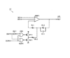
図2は、リップルインジェクション部17の一構成例を示す回路ブロック図である。図2に示すように、本構成例のリップルインジェクション部17は、アンプAMP1と、抵抗R11〜R13と、コンデンサC11と、Pチャネル型MOS電界効果トランジスタP11と、Nチャネル型MOS電界効果トランジスタN11と、インバータINV1と、論理和演算器OR1と、否定論理和演算器NOR1と、を有する。
FIG. 2 is a circuit block diagram showing a configuration example of the
アンプAMP1の第2非反転入力端(+)は、ソフトスタート電圧SSの入力端に接続されている。ソフトスタート電圧SSとは、半導体装置1の起動後、ゼロ値から所定の目標値(バンドギャップ基準電圧BGよりも高い電圧値)まで緩やかに上昇していくスロープ電圧である。アンプAMP1の第1非反転入力端(−)は、バンドギャップ基準電圧BGの入力端に接続されている。アンプAMP1の反転入力端(−)は、抵抗R11の第1端に接続されている。アンプAMP1の出力端は、リップル成分を注入された基準電圧REFの出力端に接続されている。抵抗R11の第2端は、抵抗R12の第1端、抵抗R13の第1端、及び、コンデンサC11の第1端にそれぞれ接続されている。抵抗R12の第2端、及び、コンデンサC11の第2端は、いずれもアンプAMP1の出力端に接続されている。抵抗R13の第2端は、トランジスタP11のドレイン、及び、トランジスタN11のドレインにそれぞれ接続されている。トランジスタP11のソースは、電源端に接続されている。トランジスタN11のソースは、接地端に接続されている。トランジスタP11のゲートは、論理和演算器OR1の出力端に接続されている。トランジスタN11のゲートは、否定論理和演算器NOR1の出力端に接続されている。論理和演算器OR1の第1入力端は、インバータINV1の出力端に接続されている。インバータINV1の入力端、及び、否定論理和演算器NOR1の第1入力端は、いずれもスイッチ電圧SWの入力端に接続されている。論理和演算器OR1の第2入力端、及び、否定論理和演算器NOR1の第2入力端は、いずれも過電流保護信号OCPの入力端に接続されている。過電流保護信号OCPとは、トランジスタ11、トランジスタ12、または、インダクタL1に流れる電流が過電流状態となったときにハイレベルとなる異常保護信号である。
The second non-inverting input terminal (+) of the amplifier AMP1 is connected to the input terminal of the soft start voltage SS. The soft start voltage SS is a slope voltage that gradually increases from a zero value to a predetermined target value (voltage value higher than the band gap reference voltage BG) after the
上記構成から成るリップルインジェクション部17において、抵抗R11〜R13、コンデンサC11、トランジスタP11及びN11、インバータINV1、論理和演算器OR1、並びに、否定論理和演算器NOR1は、スイッチ電圧SWに応じてアンプAMP1の負帰還ループをパルス駆動するパルス駆動部として機能する。このような構成とすることにより、アンプAMP1から出力される基準電圧REFは、バンドギャップ基準電圧BGを基準として電圧値が変動する波形、すなわち、バンドギャップ基準電圧BGにリップル成分が注入された波形となる(図3の上から2段目を参照)。ただし、半導体装置1の起動後、ソフトスタート電圧SSがバンドギャップ基準電圧BGよりも低いソフトスタート期間中には、緩やかに上昇するソフトスタート電圧SSにリップル成分を注入した基準電圧REFが生成される。
In the
再び図1に戻り、半導体装置1に集積化された回路ブロックの説明を続ける。
Returning to FIG. 1 again, the description of the circuit blocks integrated in the
バンドギャップ電源部18は、電源電圧や周囲温度の変動に依存しない所定のバンドギャップ基準電圧BG(例えば1.2V)を生成する。
The band gap
オフセット調整部20は、帰還電圧FBに基づいてバンドギャップ電源部18のオフセット調整信号ADJを生成する回路ブロックであり、エラーアンプ21と、直流電圧源22と、を有する。エラーアンプ21は、外部端子T2から反転入力端(−)に入力される帰還電圧FBと、直流電圧源22から非反転入力端(+)に入力される所定の目標電圧REF2との差分を増幅し、これをオフセット調整信号ADJとして出力する。
The offset
バンドギャップ電源部18は、オフセット調整部20から入力されるオフセット調整信号ADJに基づいて、バンドギャップ基準電圧BGの電圧値を調整する。より具体的に述べると、バンドギャップ電源部18は、帰還電圧FBが目標電圧REF2よりも低く、オフセット調整信号ADJの電圧値が高いほど、バンドギャップ基準電圧BGの電圧値を高く設定する。その結果、リップル成分を注入された基準電圧REFのDC値も高くなるので、出力電圧OUT(延いては帰還電圧FB)をより高めるように帰還制御がかかる。
The band gap
このように、オフセット調整部20では、帰還電圧FBと所定の目標電圧REF2とが一致するように、バンドギャップ電源部18のオフセット調整信号ADJが生成される。従って、図4に示したように、リップル成分を注入された基準電圧REFのDC値(REFDC)がスイッチ電圧SWのデューティに応じて変動し、これに起因して出力電圧OUT(延いては、帰還電圧FB)に意図しないDCオフセットが生じた場合であっても、このDCオフセットをキャンセルするように、バンドギャップ基準電圧BGの電圧値を自動調整することができるので、出力電圧精度やロードレギュレーション特性を向上させることが可能となる。
As described above, the offset
また、従来では、出力電圧精度やロードレギュレーション特性の悪化を懸念して、リップルインジェクション量が抑えられていたが、上記構成を採用することにより、出力電圧精度やロードレギュレーション特性を悪化させることなく、リップルインジェクション量を増やすことができるので、スイッチング動作の安定性やジッタ特性の向上を図ることが可能となる。 Conventionally, the ripple injection amount has been suppressed due to concerns about deterioration of output voltage accuracy and load regulation characteristics, but by adopting the above configuration, output voltage accuracy and load regulation characteristics are not deteriorated. Since the amount of ripple injection can be increased, it is possible to improve the stability of the switching operation and the jitter characteristics.
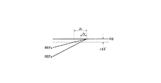
図5は、リップルインジェクション量とジッタ量との関係を示す模式図である。リップルインジェクション量の小さい基準電圧REFxと帰還電圧FBとの交差角度よりも、リップルインジェクション量の大きい基準電圧REFyと帰還電圧FBとの交差角度の方がより大きく(深く)なる。従って、例えば、帰還電圧FBの変動(図5の破線を参照)に起因する比較信号CMPのジッタ成分を考えた場合、REFx入力時のジッタ成分JxよりもREFy入力時のジッタ成分Jyの方がより小さくなる。このように、ジッタ特性の向上を図るためには、リップルインジェクション量を増やすことが有効であると言える。 FIG. 5 is a schematic diagram showing the relationship between the ripple injection amount and the jitter amount. The crossing angle between the reference voltage REFy having a large ripple injection amount and the feedback voltage FB is larger (deeper) than the crossing angle between the reference voltage REFx having a small ripple injection amount and the feedback voltage FB. Therefore, for example, when considering the jitter component of the comparison signal CMP due to the fluctuation of the feedback voltage FB (see the broken line in FIG. 5), the jitter component Jy at the time of REFy input is more than the jitter component Jx at the time of REFx input. Smaller. Thus, it can be said that increasing the ripple injection amount is effective for improving the jitter characteristics.
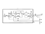
(第2実施形態)
図6は、本発明に係るスイッチング電源装置の第2実施形態を示す回路ブロック図である。第2実施形態は、先出の第1実施形態と基本的には同一の構成から成るが、リップル成分を帰還電圧FBに注入している点と、リップル注入後の帰還電圧FB2をモニタしてリップルインジェクション部17のオフセット調整信号ADJを生成している点に特徴を有している。そこで、第1実施形態と同様の構成要素については、図1と同一の符号を付すことで重複した説明を割愛し、以下では、第2実施形態の特徴部分について重点的な説明を行う。
(Second Embodiment)
FIG. 6 is a circuit block diagram showing a second embodiment of the switching power supply device according to the present invention. The second embodiment basically has the same configuration as the first embodiment, but the ripple component is injected into the feedback voltage FB and the feedback voltage FB2 after the ripple injection is monitored. It is characterized in that the offset adjustment signal ADJ of the
コンパレータ16は、リップルインジェクション部17から反転入力端(−)に入力されるリップル注入済みの帰還電圧FB2と、バンドギャップ電源部18から非反転入力端(+)に入力されるバンドギャップ基準電圧BGを比較して比較信号CMPを出力する。すなわち、リップル注入後の帰還電圧FB2がバンドギャップ基準電圧BGよりも高ければ、比較信号CMPはローレベルとなり、逆に、リップル注入後の帰還電圧FB2がバンドギャップ基準電圧BGよりも低ければ、比較信号CMPはハイレベルとなる。
The
リップルインジェクション部17は、スイッチ電圧SWを利用してリップル成分を生成し、これを帰還電圧FBに注入する。
The
オフセット調整部30は、リップル注入後の帰還電圧FB2からリップルインジェクション部17のオフセット調整信号FB2DCを生成する。具体的に述べると、オフセット調整部30は、リップル注入後の帰還電圧FB2を平滑化して平滑帰還電圧FB2DCを生成するCRフィルタと、平滑帰還電圧FB2DCと所定の目標電圧REF3とが一致するようにオフセット調整信号ADJを生成し、これをリップルインジェクション部17に出力するエラーアンプと、を有する(図6ではいずれも不図示)。
The offset
このような構成とすることにより、先出の第1実施形態と同様の作用・効果を奏することが可能となる。 By adopting such a configuration, it is possible to achieve the same operations and effects as in the first embodiment.
(第3実施形態)
図7は、本発明に係るスイッチング電源装置の第3実施形態を示す回路ブロック図である。第3実施形態は、先出の第1実施形態と基本的には同一の構成から成るが、リップル注入後の基準電圧REFをモニタしてリップルインジェクション部17のオフセット調整信号ADJを生成している点に特徴を有している。そこで、第1実施形態と同様の構成要素については、図1と同一の符号を付すことで重複した説明を割愛し、以下では、第3実施形態の特徴部分について重点的な説明を行う。
(Third embodiment)
FIG. 7 is a circuit block diagram showing a third embodiment of the switching power supply device according to the present invention. The third embodiment has basically the same configuration as the first embodiment, but generates the offset adjustment signal ADJ of the
先にも述べたように、オフセット調整部40は、帰還電圧FBではなく、リップル注入後の基準電圧REFに基づいて、リップルインジェクション部17のオフセット調整信号ADJを生成する。
As described above, the offset
図8は、オフセット調整部40の一構成例を示す回路ブロック図である。本構成例のオフセット調整部40は、アンプAMP2と、抵抗R21及びR22と、コンデンサC21〜C23と、を有する。
FIG. 8 is a circuit block diagram illustrating a configuration example of the offset
抵抗R21の第1端は、アンプAMP1の出力端に接続されている。抵抗R21の第2端は、抵抗R22の第1端と、コンデンサC21の第1端と、コンデンサC23の第1端に各々接続されている。コンデンサC21の第2端は、接地端に接続されている。抵抗R22の第2端、コンデンサC22の第1端、及び、コンデンサC23の第2端は、いずれもアンプAMP2の非反転入力端(+)に接続されている。コンデンサC22の第2端は接地端に接続されている。アンプAMP2の反転入力端(−)は、バンドギャップ基準電圧BGの入力端に接続されている。アンプAMP2の非反転出力端(+)は、非反転オフセット調整信号ADJPの出力端として、アンプAMP1に接続されている。アンプAMP2の反転出力端(−)は、反転オフセット調整信号ADJMの出力端として、アンプAMP1に接続されている。 The first end of the resistor R21 is connected to the output end of the amplifier AMP1. The second end of the resistor R21 is connected to the first end of the resistor R22, the first end of the capacitor C21, and the first end of the capacitor C23. The second end of the capacitor C21 is connected to the ground end. The second end of the resistor R22, the first end of the capacitor C22, and the second end of the capacitor C23 are all connected to the non-inverting input terminal (+) of the amplifier AMP2. The second end of the capacitor C22 is connected to the ground end. The inverting input terminal (−) of the amplifier AMP2 is connected to the input terminal of the band gap reference voltage BG. The non-inverting output terminal (+) of the amplifier AMP2 is connected to the amplifier AMP1 as the output terminal of the non-inverting offset adjustment signal ADJP. The inverting output terminal (−) of the amplifier AMP2 is connected to the amplifier AMP1 as the output terminal of the inverting offset adjustment signal ADJM.
すなわち、本構成例のオフセット調整部40は、リップル注入後の基準電圧REFを平滑化して平滑基準電圧REFDCを生成するCRフィルタ(抵抗R21及びR22、並びに、コンデンサC21〜C23)と、リップル注入前のバンドギャップ基準電圧BGと平滑基準電圧REFDCとが一致するようにオフセット調整信号ADJP及びADJMを生成し、これをアンプAMP1に出力するアンプAMP2と、を有する構成とされている。
That is, the offset
図9は、アンプAMP1の一構成例を示す回路図である。本構成例のアンプAMP1はnpn型バイポーラトランジスタQ11及びQ12と、pnp型バイポーラトランジスタQ13〜Q15と、Pチャネル型MOS電界効果トランジスタP21と、抵抗R31〜R39と、定電流源I1及びI2と、を有する。 FIG. 9 is a circuit diagram illustrating a configuration example of the amplifier AMP1. The amplifier AMP1 of this configuration example includes npn-type bipolar transistors Q11 and Q12, pnp-type bipolar transistors Q13 to Q15, P-channel MOS field effect transistors P21, resistors R31 to R39, and constant current sources I1 and I2. Have.
トランジスタQ11及びQ12のコレクタは、それぞれ、抵抗R32及びR33を介して電源端に接続されている。トランジスタQ11及びQ12のエミッタは、互いに接続されており、その接続ノードは、定電流源I1を介して接地端に接続されている。 The collectors of the transistors Q11 and Q12 are connected to the power supply terminal via resistors R32 and R33, respectively. The emitters of the transistors Q11 and Q12 are connected to each other, and the connection node is connected to the ground terminal via the constant current source I1.
トランジスタQ11のベースは、抵抗R37の第1端と、反転オフセット調整信号ADJMの入力端と、にそれぞれ接続されている。抵抗R37の第2端は、抵抗R31を介して電源端に接続される一方、抵抗R35及びR36を各々介してトランジスタQ13及びQ14の各エミッタにも接続されている。トランジスタQ13及びQ14のコレクタは互いに接続されており、その接続ノードは接地端に接続されている。トランジスタQ13のベースは、アンプAMP1の第2非反転入力端INP2に相当し、ソフトスタート電圧SSの入力端に接続されている。トランジスタQ14のベースは、アンプAMP1の第1非反転入力端INP1に相当し、バンドギャップ基準電圧BGの入力端に接続されている。 The base of the transistor Q11 is connected to the first end of the resistor R37 and the input end of the inverted offset adjustment signal ADJM. The second end of the resistor R37 is connected to the power supply end via the resistor R31, and is also connected to the emitters of the transistors Q13 and Q14 via the resistors R35 and R36, respectively. The collectors of the transistors Q13 and Q14 are connected to each other, and the connection node is connected to the ground terminal. The base of the transistor Q13 corresponds to the second non-inverting input terminal INP2 of the amplifier AMP1, and is connected to the input terminal of the soft start voltage SS. The base of the transistor Q14 corresponds to the first non-inverting input terminal INP1 of the amplifier AMP1, and is connected to the input terminal of the band gap reference voltage BG.
トランジスタQ12のベースは、抵抗R38の第1端と、非反転オフセット調整信号ADJPの入力端と、にそれぞれ接続されている。抵抗R38の第2端は、抵抗R34を介して電源端に接続される一方、抵抗R39を介してトランジスタQ15のエミッタにも接続されている。トランジスタQ15のコレクタは、接地端に接続されている。トランジスタQ15のベースは、アンプAMP1の反転入力端INNに相当する。 The base of the transistor Q12 is connected to the first end of the resistor R38 and the input end of the non-inverted offset adjustment signal ADJP. The second end of the resistor R38 is connected to the power supply end via the resistor R34, and is also connected to the emitter of the transistor Q15 via the resistor R39. The collector of the transistor Q15 is connected to the ground terminal. The base of the transistor Q15 corresponds to the inverting input terminal INN of the amplifier AMP1.
トランジスタP21のソースは、電源端に接続されている。トランジスタP21のドレインは、リップル成分が注入された基準電圧REFの出力端に接続される一方、定電流源I2を介して接地端にも接続されている。トランジスタP21のゲートは、トランジスタQ11のコレクタに接続されている。 The source of the transistor P21 is connected to the power supply terminal. The drain of the transistor P21 is connected to the output terminal of the reference voltage REF into which the ripple component is injected, and is also connected to the ground terminal via the constant current source I2. The gate of the transistor P21 is connected to the collector of the transistor Q11.
図10は、アンプAMP2の一構成例を示す回路図である。本構成例のアンプAMP2は、Pチャネル型MOS電界効果トランジスタP31〜P37と、Nチャネル型MOS電界効果トランジスタN21〜N24と、を有する。 FIG. 10 is a circuit diagram illustrating a configuration example of the amplifier AMP2. The amplifier AMP2 of this configuration example includes P-channel MOS field effect transistors P31 to P37 and N-channel MOS field effect transistors N21 to N24.
トランジスタP31〜P33の各ソースは互いに接続されており、その接続ノードは、定電流源I3を介して電源端に接続されている。トランジスタP31及びP32のドレインは互いに接続されており、その接続ノードは、トランジスタN23のドレインに接続されている。トランジスタP33のドレインは、トランジスタN21のドレインに接続されている。トランジスタP31のゲートは、アンプAMP2の第1反転入力端INN1に相当し、バンドギャップ基準電圧BGの入力端に接続されている。トランジスタP32のゲートは、アンプAMP2の第2反転入力端INN2に相当し、ソフトスタート電圧SSの入力端に接続されている。トランジスタP33のゲートは、アンプAMP2の非反転入力端INPに相当し、平滑基準電圧REFDCの入力端に接続されている。 The sources of the transistors P31 to P33 are connected to each other, and the connection node is connected to the power supply terminal via the constant current source I3. The drains of the transistors P31 and P32 are connected to each other, and the connection node is connected to the drain of the transistor N23. The drain of the transistor P33 is connected to the drain of the transistor N21. The gate of the transistor P31 corresponds to the first inverting input terminal INN1 of the amplifier AMP2, and is connected to the input terminal of the bandgap reference voltage BG. The gate of the transistor P32 corresponds to the second inverting input terminal INN2 of the amplifier AMP2, and is connected to the input terminal of the soft start voltage SS. The gate of the transistor P33 corresponds to the non-inverting input terminal INP of the amplifier AMP2, and is connected to the input terminal of the smoothing reference voltage REFDC.
トランジスタN21及びN22のゲートは、いずれもトランジスタN21のドレインに接続されている。トランジスタN21及びN22のソースは、いずれも接地端に接続されている。トランジスタN22のドレインは、トランジスタP34のドレインに接続されている。トランジスタP34及びP35のゲートは、いずれもトランジスタP34のドレインに接続されている。トランジスタP34及びP35のソースは、いずれも電源端に接続されている。トランジスタP35のドレインは、反転オフセット調整信号ADJMの出力端に接続されている。 The gates of the transistors N21 and N22 are both connected to the drain of the transistor N21. The sources of the transistors N21 and N22 are both connected to the ground terminal. The drain of the transistor N22 is connected to the drain of the transistor P34. The gates of the transistors P34 and P35 are both connected to the drain of the transistor P34. The sources of the transistors P34 and P35 are both connected to the power supply terminal. The drain of the transistor P35 is connected to the output terminal of the inverted offset adjustment signal ADJM.
トランジスタN23及びN24のゲートは、いずれもトランジスタN23のドレインに接続されている。トランジスタN23及びN24のソースは、いずれも接地端に接続されている。トランジスタN24のドレインは、トランジスタP36のドレインに接続されている。トランジスタP36及びP37のゲートは、いずれもトランジスタP36のドレインに接続されている。トランジスタP36及びP37のソースは、いずれも電源端に接続されている。トランジスタP37のドレインは、非反転オフセット調整信号ADJPの出力端に接続されている。 The gates of the transistors N23 and N24 are both connected to the drain of the transistor N23. The sources of the transistors N23 and N24 are both connected to the ground terminal. The drain of the transistor N24 is connected to the drain of the transistor P36. The gates of the transistors P36 and P37 are both connected to the drain of the transistor P36. The sources of the transistors P36 and P37 are both connected to the power supply terminal. The drain of the transistor P37 is connected to the output terminal of the non-inverting offset adjustment signal ADJP.
このような構成とすることにより、先出の第1実施形態と同様の作用・効果を奏することが可能となる。また、リップル注入後の基準電圧REFをモニタする第3実施形態であれば、帰還電圧FBをモニタする第1実施形態と比べて、オフセット調整ループ内の位相特性を合わせ込む作業も容易となる。 By adopting such a configuration, it is possible to achieve the same operations and effects as in the first embodiment. Further, in the third embodiment in which the reference voltage REF after ripple injection is monitored, the work of adjusting the phase characteristics in the offset adjustment loop is also easier than in the first embodiment in which the feedback voltage FB is monitored.
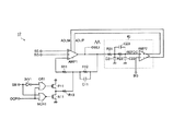
(第4実施形態)
図11は、本発明に係るスイッチング電源装置の第4実施形態を示す回路ブロック図である。第4実施形態は、先出の第1実施形態や第3実施形態と基本的には同一の構成から成るが、帰還電圧FBをモニタしてリップルインジェクション部17のオフセット調整信号ADJを生成するオフセット調整部50を有する点に特徴を有している。すなわち、オフセット調整部50で帰還電圧FBをモニタする点を鑑みれば、第4実施形態は第1実施形態と類似しており、また、リップルインジェクション部17のオフセット調整を行う点を鑑みれば、第4実施形態は第3実施形態と類似している。
(Fourth embodiment)
FIG. 11 is a circuit block diagram showing a fourth embodiment of the switching power supply device according to the present invention. The fourth embodiment has basically the same configuration as the first and third embodiments described above, but is configured to monitor the feedback voltage FB and generate the offset adjustment signal ADJ of the
なお、リップルインジェクション部17やこれに含まれるアンプAMP1の構成及び動作については、第1実施形態や第3実施形態(図2、図8、及び、図9を参照)と同様である。また、オフセット調整部50の構成及び動作については、第1実施形態のオフセット調整部20(図1を参照)と同様である。
The configuration and operation of the
このような構成とすることにより、半導体装置1の内部でオフセット調整ループが閉じている第3実施形態と比べて、出力電圧OUTの挙動をより反映した帰還制御を行うことが可能となる。
By adopting such a configuration, it is possible to perform feedback control more reflecting the behavior of the output voltage OUT, compared to the third embodiment in which the offset adjustment loop is closed inside the
(その他の変形例)
なお、上記の実施形態では、ボトム検出オン時間固定方式を採用したスイッチング電源装置に本発明を適用した構成を例に挙げて説明を行ったが、本発明の適用対象はこれに限定されるものではなく、本発明は、その他の非線形制御方式(ヒステリシス・ウィンドウ方式やアッパー検出オフ時間固定方式など)を採用したスイッチング電源装置にも広く適用することが可能である。
(Other variations)
In the above embodiment, the configuration in which the present invention is applied to the switching power supply apparatus adopting the bottom detection on-time fixed method has been described as an example, but the scope of application of the present invention is limited to this. Instead, the present invention can be widely applied to switching power supply devices that employ other nonlinear control methods (such as a hysteresis window method and an upper detection off-time fixed method).
また、本発明の構成は、上記実施形態のほか、発明の主旨を逸脱しない範囲で種々の変更を加えることが可能である。すなわち、上記実施形態は、全ての点で例示であって、制限的なものではないと考えられるべきであり、本発明の技術的範囲は、上記実施形態の説明ではなく、特許請求の範囲によって示されるものであり、特許請求の範囲と均等の意味及び範囲内に属する全ての変更が含まれると理解されるべきである。 The configuration of the present invention can be variously modified within the scope of the present invention in addition to the above embodiment. That is, the above-described embodiment is an example in all respects and should not be considered as limiting, and the technical scope of the present invention is not the description of the above-described embodiment, but the claims. It should be understood that all modifications that come within the meaning and range of equivalents of the claims are included.
本発明に係るスイッチング電源装置は、パーソナルコンピュータ、液晶テレビ、DVDレコーダなどに好適に利用することが可能である。 The switching power supply device according to the present invention can be suitably used for personal computers, liquid crystal televisions, DVD recorders, and the like.
1 半導体装置(スイッチング電源IC)
11 Nチャネル型MOS電界効果トランジスタ(出力トランジスタ)
12 Nチャネル型MOS電界効果トランジスタ(同期整流トランジスタ)
13 ドライバ
14 SRフリップフロップ
15 オン時間設定部
16 コンパレータ
17 リップルインジェクション部
18 バンドギャップ電源部
20 オフセット調整部
21 エラーアンプ
22 直流電圧源
30 オフセット調整部
40 オフセット調整部
50 オフセット調整部
L1 インダクタ
R1、R2、R11〜R13、R21、R22、R31〜R39 抵抗
C1、C11、C21〜C23 コンデンサ
AMP1、AMP2 アンプ
P11、P21、P31〜P37 Pチャネル型MOS電界効果トランジスタ
N11、N21〜N24 Nチャネル型MOS電界効果トランジスタ
OR1 論理和演算器
NOR1 否定論理和演算器
INV1 インバータ
Q11、Q12 npn型バイポーラトランジスタ
Q13〜Q15 pnp型バイポーラトランジスタ
I1〜I3 定電流源
1 Semiconductor device (switching power supply IC)
11 N-channel MOS field effect transistor (output transistor)
12 N-channel MOS field effect transistor (synchronous rectification transistor)
DESCRIPTION OF
Claims (6)
スイッチ素子の一端に現れるスイッチ電圧を利用してリップル成分を生成し、これを前記基準電圧に注入するリップルインジェクション部と;
出力電圧に応じた帰還電圧とリップル注入後の前記基準電圧とを比較するコンパレータと;
前記コンパレータの出力信号に基づいて前記スイッチ素子のオン/オフ制御を行うことにより、入力電圧から前記出力電圧を生成する非線形制御方式のスイッチング制御部と;
前記リップル成分に起因する前記出力電圧のDCオフセットをキャンセルするように、リップル注入後の前記基準電圧に基づいて前記リップルインジェクション部のオフセット調整信号を生成するオフセット調整部と;
を有し、
前記リップルインジェクション部は、
その非反転入力端がリップル注入前の前記基準電圧の入力端に接続され、その反転入力端とその出力端とが互いに接続され、その出力端からリップル注入後の前記基準電圧が出力される第1アンプと;
前記第1アンプの反転入力端及び出力端と前記スイッチ電圧の入力端との間に接続されたパルス駆動部と;
を含み、
前記オフセット調整部は、
リップル注入後の前記基準電圧を平滑化して平滑基準電圧を生成するフィルタと;
リップル注入前の前記基準電圧と前記平滑基準電圧とが一致するように前記オフセット調整信号を生成し、これを前記第1アンプに出力する第2アンプと;
を含むことを特徴とするスイッチング電源装置。 A reference voltage generator for generating a reference voltage;
A ripple injection unit that generates a ripple component using a switch voltage appearing at one end of the switch element and injects the ripple component into the reference voltage;
A comparator that compares the feedback voltage according to the output voltage with the reference voltage after ripple injection;
A non-linear control type switching control unit that generates the output voltage from an input voltage by performing on / off control of the switch element based on an output signal of the comparator;
An offset adjustment unit that generates an offset adjustment signal of the ripple injection unit based on the reference voltage after ripple injection so as to cancel a DC offset of the output voltage caused by the ripple component;
Have
The ripple injection part is
The non-inverting input terminal is connected to the input terminal of the reference voltage before ripple injection, the inverting input terminal and the output terminal are connected to each other, and the reference voltage after ripple injection is output from the output terminal. With 1 amp;
A pulse driver connected between an inverting input terminal and an output terminal of the first amplifier and an input terminal of the switch voltage;
Including
The offset adjuster is
A filter that smoothes the reference voltage after ripple injection to generate a smoothed reference voltage;
A second amplifier that generates the offset adjustment signal so that the reference voltage before ripple injection and the smoothed reference voltage match, and outputs the offset adjustment signal to the first amplifier;
A switching power supply device comprising:
前記スイッチ電圧は、前記出力トランジスタと前記同期整流トランジスタとの接続ノードに現れる電圧であることを特徴とする請求項1に記載のスイッチング電源装置。 The switching power supply device according to claim 1, wherein the switch voltage is a voltage that appears at a connection node between the output transistor and the synchronous rectification transistor.
一対を成すようにそれぞれのエミッタが互いに接続されたnpn型の第1トランジスタ及び第2トランジスタと; An npn-type first transistor and a second transistor whose emitters are connected to each other so as to form a pair;
コレクタが接地端に接続されてベースが前記第1アンプの第2非反転入力端に相当するpnp型の第3トランジスタと; A pnp-type third transistor having a collector connected to the ground terminal and a base corresponding to a second non-inverting input terminal of the first amplifier;
コレクタが接地端に接続されてベースが前記第1アンプの第1非反転入力端に相当するpnp型の第4トランジスタと; A pnp-type fourth transistor having a collector connected to the ground terminal and a base corresponding to a first non-inverting input terminal of the first amplifier;
コレクタが接地端に接続されてベースが前記第1アンプの反転入力端に相当するpnp型の第5トランジスタと; A pnp-type fifth transistor having a collector connected to the ground terminal and a base corresponding to the inverting input terminal of the first amplifier;
第1端が電源端に接続された第1抵抗と; A first resistor having a first end connected to a power supply end;
第1端が電源端に接続されて第2端が前記第1トランジスタのコレクタに接続された第2抵抗と; A second resistor having a first end connected to the power supply end and a second end connected to the collector of the first transistor;
第1端が電源端に接続されて第2端が前記第2トランジスタのコレクタに接続された第3抵抗と; A third resistor having a first end connected to the power supply end and a second end connected to the collector of the second transistor;
第1端が電源端に接続された第4抵抗と; A fourth resistor having a first end connected to the power supply end;
第1端が前記第1抵抗の第2端に接続されて第2端が前記第3トランジスタのエミッタに接続された第5抵抗と; A fifth resistor having a first end connected to the second end of the first resistor and a second end connected to the emitter of the third transistor;
第1端が前記第1抵抗の第2端に接続されて第2端が前記第4トランジスタのエミッタに接続された第6抵抗と; A sixth resistor having a first end connected to the second end of the first resistor and a second end connected to the emitter of the fourth transistor;
第1端が前記第1抵抗の第2端に接続されて第2端が前記第1トランジスタのベースに接続された第7抵抗と; A seventh resistor having a first end connected to a second end of the first resistor and a second end connected to a base of the first transistor;
第1端が前記第2トランジスタのベースに接続されて第2端が前記第4抵抗の第2端に接続された第8抵抗と; An eighth resistor having a first end connected to a base of the second transistor and a second end connected to a second end of the fourth resistor;
第1端が前記第4抵抗の第2端に接続されて第2端が前記第5トランジスタのエミッタに接続された第9抵抗と; A ninth resistor having a first end connected to the second end of the fourth resistor and a second end connected to the emitter of the fifth transistor;
ソースが電源端に接続され、ゲートが前記第1トランジスタのコレクタに接続され、ドレインが前記第1アンプの出力端に相当するPMOSFETと; A PMOSFET whose source is connected to the power supply terminal, whose gate is connected to the collector of the first transistor, and whose drain corresponds to the output terminal of the first amplifier;
前記第1トランジスタ及び前記第2トランジスタの各エミッタと接地端との間に接続された第1電流源と; A first current source connected between each emitter of the first transistor and the second transistor and a ground terminal;
前記PMOSFETのドレインと接地端との間に接続された第2電流源と; A second current source connected between the drain of the PMOSFET and a ground terminal;
を含み、 Including
前記オフセット調整信号は、 The offset adjustment signal is
前記第1トランジスタのベースに入力される反転オフセット調整信号と、 An inverted offset adjustment signal input to the base of the first transistor;
前記第2トランジスタのベースに入力される非反転オフセット調整信号と、 A non-inverting offset adjustment signal input to the base of the second transistor;
を含むことを特徴とする請求項1または請求項2に記載のスイッチング電源装置。 The switching power supply device according to claim 1, further comprising:
ゲートが前記第2アンプの第1反転入力端に相当する第1PMOSFETと; A first PMOSFET whose gate corresponds to a first inverting input terminal of the second amplifier;
前記第1PMOSFETと並列に接続されてゲートが前記第2アンプの第2反転入力端に相当する第2PMOSFETと; A second PMOSFET connected in parallel with the first PMOSFET and having a gate corresponding to a second inverting input terminal of the second amplifier;
ソースが前記第1PMOSFETのソースと接続されてゲートが前記第2アンプの非反転入力端に相当する第3PMOSFETと; A third PMOSFET having a source connected to the source of the first PMOSFET and a gate corresponding to a non-inverting input terminal of the second amplifier;
前記第1PMOSFET及び前記第3PMOSFETの各ソースと電源端との間に接続された電流源と; A current source connected between each source of the first PMOSFET and the third PMOSFET and a power supply end;
ドレインとゲートがいずれも前記第3PMOSFETのドレインに接続されてソースが接地端に接続された第1NMOSFETと; A first NMOSFET whose drain and gate are both connected to the drain of the third PMOSFET and whose source is connected to the ground terminal;
ゲートが前記第1NMOSFETのゲートに接続されてソースが接地端に接続された第2NMOSFETと; A second NMOSFET having a gate connected to the gate of the first NMOSFET and a source connected to a ground terminal;
ドレインとゲートがいずれも第2NMOSFETのドレインに接続されてソースが電源端に接続された第4PMOSFETと; A fourth PMOSFET having both a drain and a gate connected to the drain of the second NMOSFET and a source connected to the power supply terminal;
ゲートが前記第4PMOSFETのゲートに接続され、ソースが電源端に接続され、ドレインが反転オフセット調整信号の出力端に相当する第5PMOSFETと; A fifth PMOSFET having a gate connected to the gate of the fourth PMOSFET, a source connected to the power supply terminal, and a drain corresponding to the output terminal of the inverted offset adjustment signal;
ドレインとゲートがいずれも前記第1PMOSFET及び前記第2PMOSFETの各ドレインに接続されてソースが接地端に接続された第3NMOSFETと; A third NMOSFET whose drain and gate are both connected to the drains of the first PMOSFET and the second PMOSFET and whose source is connected to the ground terminal;
ゲートが前記第3NMOSFETのゲートに接続されてソースが接地端に接続された第4NMOSFETと; A fourth NMOSFET having a gate connected to the gate of the third NMOSFET and a source connected to a ground terminal;
ドレインとゲートがいずれも第4NMOSFETのドレインに接続されてソースが電源端に接続された第6PMOSFETと; A sixth PMOSFET having both a drain and a gate connected to the drain of the fourth NMOSFET and a source connected to the power supply terminal;
ゲートが前記第6PMOSFETのゲートに接続され、ソースが電源端に接続され、ドレインが非反転オフセット調整信号の出力端に相当する第7PMOSFETと; A seventh PMOSFET having a gate connected to the gate of the sixth PMOSFET, a source connected to the power supply terminal, and a drain corresponding to the output terminal of the non-inverting offset adjustment signal;
を含むことを特徴とする請求項1〜請求項3のいずれか一項に記載のスイッチング電源装置。 The switching power supply device according to any one of claims 1 to 3, wherein the switching power supply device includes:
第1端が前記第1アンプの出力端に接続された第1フィルタ抵抗と; A first filter resistor having a first end connected to the output end of the first amplifier;
第1端が前記第1フィルタ抵抗の第2端に接続されて第2端が前記第2アンプの非反転入力端に接続された第2フィルタ抵抗と; A second filter resistor having a first end connected to a second end of the first filter resistor and a second end connected to a non-inverting input end of the second amplifier;
前記第1フィルタ抵抗の第2端と接地端との間に接続された第1コンデンサと; A first capacitor connected between a second end of the first filter resistor and a ground end;
前記第2フィルタ抵抗の第2端と接地端との間に接続された第2コンデンサと; A second capacitor connected between a second end of the second filter resistor and a ground end;
前記第2フィルタ抵抗に対して並列に接続された第3コンデンサと; A third capacitor connected in parallel with the second filter resistor;
を含むことを特徴とする請求項1〜請求項5のいずれか一項に記載のスイッチング電源装置。 The switching power supply device according to claim 1, wherein the switching power supply device includes:
Priority Applications (3)
| Application Number | Priority Date | Filing Date | Title |
|---|---|---|---|
| JP2011081485A JP5771429B2 (en) | 2010-05-28 | 2011-04-01 | Switching power supply |
| US13/116,226 US8604769B2 (en) | 2010-05-28 | 2011-05-26 | Switching power source device |
| CN201110146990.6A CN102290986B (en) | 2010-05-28 | 2011-05-27 | Switching power unit |
Applications Claiming Priority (3)
| Application Number | Priority Date | Filing Date | Title |
|---|---|---|---|
| JP2010122270 | 2010-05-28 | ||
| JP2010122270 | 2010-05-28 | ||
| JP2011081485A JP5771429B2 (en) | 2010-05-28 | 2011-04-01 | Switching power supply |
Publications (2)
| Publication Number | Publication Date |
|---|---|
| JP2012010579A JP2012010579A (en) | 2012-01-12 |
| JP5771429B2 true JP5771429B2 (en) | 2015-08-26 |
Family
ID=45021543
Family Applications (1)
| Application Number | Title | Priority Date | Filing Date |
|---|---|---|---|
| JP2011081485A Active JP5771429B2 (en) | 2010-05-28 | 2011-04-01 | Switching power supply |
Country Status (3)
| Country | Link |
|---|---|
| US (1) | US8604769B2 (en) |
| JP (1) | JP5771429B2 (en) |
| CN (1) | CN102290986B (en) |
Families Citing this family (38)
| Publication number | Priority date | Publication date | Assignee | Title |
|---|---|---|---|---|
| JP5703671B2 (en) * | 2010-10-05 | 2015-04-22 | 富士通セミコンダクター株式会社 | Power controller and electronic device |
| JP5749483B2 (en) * | 2010-12-10 | 2015-07-15 | ローム株式会社 | Hysteresis control switching regulator control circuit, hysteresis control switching regulator using the control circuit, and electronic equipment |
| CN102751872B (en) * | 2011-04-21 | 2016-04-06 | 登丰微电子股份有限公司 | Feedback control circuit |
| JP5768475B2 (en) * | 2011-04-28 | 2015-08-26 | ミツミ電機株式会社 | Switching power supply |
| JP6009742B2 (en) * | 2011-08-08 | 2016-10-19 | ローム株式会社 | Switching power supply |
| JP5870712B2 (en) * | 2012-01-31 | 2016-03-01 | ローム株式会社 | Electric circuit having FET, switching regulator, and electric device |
| CN102611306B (en) * | 2012-03-27 | 2015-12-16 | 成都芯源系统有限公司 | Switch converter and control circuit and control method thereof |
| US8982587B2 (en) * | 2012-04-23 | 2015-03-17 | Hamilton Sundstrand Corporation | Compensating ripple on pulse with modulator outputs |
| CN103390992B (en) * | 2012-05-10 | 2015-09-30 | 华润矽威科技(上海)有限公司 | Switching Power Supply and improve the circuit of its output current regulation |
| JP6013052B2 (en) * | 2012-07-04 | 2016-10-25 | ローム株式会社 | Switching power supply |
| JP6029062B2 (en) * | 2013-01-18 | 2016-11-24 | ローム株式会社 | Switching power supply |
| JP6093144B2 (en) * | 2012-05-14 | 2017-03-08 | ローム株式会社 | Switching power supply |
| US8842225B2 (en) * | 2012-05-14 | 2014-09-23 | Rohm Co., Ltd. | Switching power supply device |
| JP6122257B2 (en) * | 2012-07-04 | 2017-04-26 | ローム株式会社 | DC / DC converter and control circuit thereof, power supply using the same, power adapter, and electronic device |
| CN104904119B (en) * | 2012-10-30 | 2018-05-22 | 天工方案公司 | Spuious elimination in GSM-GPRS-EDGE power amplifiers with dc-dc |
| JP6046999B2 (en) * | 2012-12-07 | 2016-12-21 | ローム株式会社 | Switching power supply |
| US9419518B2 (en) | 2013-03-06 | 2016-08-16 | Qualcomm Incorporated | Transfer function generation based on pulse-width modulation information |
| US9423807B2 (en) * | 2013-03-06 | 2016-08-23 | Qualcomm Incorporated | Switching power converter |
| US9590501B2 (en) * | 2013-04-25 | 2017-03-07 | Fairchild Semiconductor Corporation | Fast load transient response power supply system using dynamic reference generation |
| CN104124869B (en) * | 2013-04-28 | 2017-05-10 | 艾默生网络能源系统北美公司 | Boosted circuit and signal output method |
| CN103346662B (en) * | 2013-06-20 | 2016-02-03 | 成都芯源系统有限公司 | Control circuit, switch converter and control method thereof |
| CN105745828A (en) * | 2013-09-30 | 2016-07-06 | 微电子中心德累斯顿有限公司 | Compensation free modulation for power converters |
| US9548660B2 (en) * | 2013-10-08 | 2017-01-17 | Qualcomm Incorporated | Circuit and method to compensate for equivalent series inductance (ESL) effects in a buck regulator |
| JP2015130744A (en) * | 2014-01-07 | 2015-07-16 | 株式会社東芝 | Power supply circuit |
| JP6422214B2 (en) * | 2014-01-16 | 2018-11-14 | 矢崎総業株式会社 | Switching power supply |
| JP6403954B2 (en) * | 2014-01-24 | 2018-10-10 | 矢崎総業株式会社 | Switching power supply |
| JP6376961B2 (en) * | 2014-03-11 | 2018-08-22 | エイブリック株式会社 | DC / DC converter |
| US10003265B2 (en) * | 2014-07-28 | 2018-06-19 | Rohm Co., Ltd. | Switching power supply device |
| US10076963B2 (en) | 2014-09-24 | 2018-09-18 | Rohm Co., Ltd. | Current mode control type switching power supply device |
| JP6424644B2 (en) * | 2015-01-21 | 2018-11-21 | ミツミ電機株式会社 | Semiconductor device for power control |
| CN108880249A (en) * | 2015-08-25 | 2018-11-23 | 华为技术有限公司 | Voltage conversion circuit, method and Multiphase Parallel power-supply system |
| JP2017055578A (en) * | 2015-09-10 | 2017-03-16 | 株式会社東芝 | DC-DC converter |
| US9866115B2 (en) | 2016-04-01 | 2018-01-09 | Nxp B.V. | Reduction of frequency variation for ripple based, constant-on-time DC-DC converters |
| US9941792B2 (en) | 2016-04-01 | 2018-04-10 | Nxp B.V. | DC offset correction for inductor current ripple based, constant-on-time DC-DC converters |
| JP6660238B2 (en) * | 2016-04-20 | 2020-03-11 | エイブリック株式会社 | Bandgap reference circuit and DCDC converter having the same |
| US10063140B2 (en) * | 2016-08-30 | 2018-08-28 | Astec International Limited | Control circuits for selectively applying error offsets to improve dynamic response in switching power converters |
| CN109696938B (en) * | 2017-10-21 | 2023-11-03 | 国神光电科技(上海)有限公司 | Electronic device for current source control and control method |
| US10797598B1 (en) * | 2019-07-16 | 2020-10-06 | Microchip Technology Incorporated | Calibrated ripple injection-based constant on-time buck converter with pre-bias startup in continuous conduction mode |
Family Cites Families (6)
| Publication number | Priority date | Publication date | Assignee | Title |
|---|---|---|---|---|
| US6369555B2 (en) * | 2000-05-15 | 2002-04-09 | Texas Instruments Incorporated | Integrated low ripple, high frequency hysteretic controller for DC-DC converters |
| US6583610B2 (en) * | 2001-03-12 | 2003-06-24 | Semtech Corporation | Virtual ripple generation in switch-mode power supplies |
| JP3916163B2 (en) * | 2004-02-19 | 2007-05-16 | ローム株式会社 | Current direction detection circuit and switching regulator provided with the same |
| JP2007116823A (en) * | 2005-10-20 | 2007-05-10 | Fujitsu Ltd | Circuit and method for controlling dc-dc converter |
| JP4613986B2 (en) | 2008-07-28 | 2011-01-19 | 日本テキサス・インスツルメンツ株式会社 | Switching power supply |
| US7834608B2 (en) * | 2008-11-18 | 2010-11-16 | Texas Instruments Incorporated | Feed-forward compensation for a hysteretic switching regulator |
-
2011
- 2011-04-01 JP JP2011081485A patent/JP5771429B2/en active Active
- 2011-05-26 US US13/116,226 patent/US8604769B2/en active Active
- 2011-05-27 CN CN201110146990.6A patent/CN102290986B/en active Active
Also Published As
| Publication number | Publication date |
|---|---|
| CN102290986A (en) | 2011-12-21 |
| CN102290986B (en) | 2016-05-18 |
| JP2012010579A (en) | 2012-01-12 |
| US20110291626A1 (en) | 2011-12-01 |
| US8604769B2 (en) | 2013-12-10 |
Similar Documents
| Publication | Publication Date | Title |
|---|---|---|
| JP5771429B2 (en) | Switching power supply | |
| JP5723578B2 (en) | Switching power supply | |
| JP5573454B2 (en) | Power factor improved switching power supply | |
| JP6009742B2 (en) | Switching power supply | |
| US8842225B2 (en) | Switching power supply device | |
| US8928303B2 (en) | Apparatus and methods for transient compensation of switching power regulators | |
| JP5702570B2 (en) | Operational amplifier, liquid crystal driving device using the same, parameter setting circuit, semiconductor device, and power supply device | |
| US10326364B2 (en) | Voltage regulator current load sensing | |
| JP5118940B2 (en) | Power supply | |
| TWI421662B (en) | Method for improving voltage identification (vid) transient response and voltage regulator | |
| TWI484738B (en) | Method for providing over current protection and circuit | |
| US20110127974A1 (en) | Switching control circuit and power supply apparatus | |
| TW201035712A (en) | Voltage regulator | |
| JP6093144B2 (en) | Switching power supply | |
| US9240716B2 (en) | Switching power supply circuit | |
| JP6029062B2 (en) | Switching power supply | |
| US9331575B2 (en) | Phase adjustment circuit of power converter, power converter, and control method thereof | |
| US9755510B2 (en) | Switching power supply | |
| TW201445858A (en) | Timing generator and timing signal generation method for power converter | |
| KR101774601B1 (en) | Switching regulator control circuit and switching regulator | |
| JP6286153B2 (en) | Switching power supply | |
| JP6013052B2 (en) | Switching power supply | |
| JP2005261102A (en) | Switching regulator | |
| JP2012032940A (en) | Power supply control circuit | |
| US9952616B2 (en) | Differential circuit including a current mirror |
Legal Events
| Date | Code | Title | Description |
|---|---|---|---|
| A621 | Written request for application examination |
Free format text: JAPANESE INTERMEDIATE CODE: A621 Effective date: 20140401 |
|
| A977 | Report on retrieval |
Free format text: JAPANESE INTERMEDIATE CODE: A971007 Effective date: 20150114 |
|
| A131 | Notification of reasons for refusal |
Free format text: JAPANESE INTERMEDIATE CODE: A131 Effective date: 20150310 |
|
| A521 | Request for written amendment filed |
Free format text: JAPANESE INTERMEDIATE CODE: A523 Effective date: 20150511 |
|
| RD03 | Notification of appointment of power of attorney |
Free format text: JAPANESE INTERMEDIATE CODE: A7423 Effective date: 20150511 |
|
| TRDD | Decision of grant or rejection written | ||
| A01 | Written decision to grant a patent or to grant a registration (utility model) |
Free format text: JAPANESE INTERMEDIATE CODE: A01 Effective date: 20150602 |
|
| A61 | First payment of annual fees (during grant procedure) |
Free format text: JAPANESE INTERMEDIATE CODE: A61 Effective date: 20150629 |
|
| R150 | Certificate of patent or registration of utility model |
Ref document number: 5771429 Country of ref document: JP Free format text: JAPANESE INTERMEDIATE CODE: R150 |
|
| R250 | Receipt of annual fees |
Free format text: JAPANESE INTERMEDIATE CODE: R250 |
|
| R250 | Receipt of annual fees |
Free format text: JAPANESE INTERMEDIATE CODE: R250 |
|
| R250 | Receipt of annual fees |
Free format text: JAPANESE INTERMEDIATE CODE: R250 |
|
| R250 | Receipt of annual fees |
Free format text: JAPANESE INTERMEDIATE CODE: R250 |
|
| R250 | Receipt of annual fees |
Free format text: JAPANESE INTERMEDIATE CODE: R250 |