JP5764912B2 - Capacitor and manufacturing method thereof - Google Patents
Capacitor and manufacturing method thereof Download PDFInfo
- Publication number
- JP5764912B2 JP5764912B2 JP2010251352A JP2010251352A JP5764912B2 JP 5764912 B2 JP5764912 B2 JP 5764912B2 JP 2010251352 A JP2010251352 A JP 2010251352A JP 2010251352 A JP2010251352 A JP 2010251352A JP 5764912 B2 JP5764912 B2 JP 5764912B2
- Authority
- JP
- Japan
- Prior art keywords
- anode
- cathode
- current collector
- capacitor
- collector plate
- Prior art date
- Legal status (The legal status is an assumption and is not a legal conclusion. Google has not performed a legal analysis and makes no representation as to the accuracy of the status listed.)
- Active
Links
Images


Description
本発明は、コンデンサ素子と、コンデンサ素子の外装部材を封口する封口部材にある外部端子との間の接続に関し、その接続にレーザ溶接を用いた例えば、電解コンデンサ、電気二重層コンデンサ等のコンデンサ及びその製造方法に関する。
The present invention relates to a connection between a capacitor element and an external terminal in a sealing member that seals an exterior member of the capacitor element. For example, a capacitor such as an electrolytic capacitor or an electric double layer capacitor using laser welding for the connection, and It relates to the manufacturing method.
電気二重層コンデンサ又は電解コンデンサでは、コンデンサ素子と外部端子とを電気的に接続することが必要である。この電気的な接続により、素子側の内部抵抗の低減や、接続部分の接触抵抗を低減させる対策が施されている。 In the electric double layer capacitor or electrolytic capacitor, it is necessary to electrically connect the capacitor element and the external terminal. By this electrical connection, measures are taken to reduce the internal resistance on the element side and the contact resistance of the connection portion.
このような電気的接続に関し、素子の端面に集電端子を設けること(例えば、特許文献1)、巻回素子の一方の端面に陽極集電板、他方の端面に陰極集電板を設けること(例えば、特許文献2)、巻回素子の端面に露出した集電箔を覆って集電板を備え、集電板と集電箔とを溶接接続すること(例えば、特許文献3)、また、集電板を外装ケースと素子との接続や外部端子との接続に用いること(例えば、特許文献4)が知られている。 Regarding such electrical connection, a current collecting terminal is provided on the end face of the element (for example, Patent Document 1), an anode current collecting plate is provided on one end face of the winding element, and a cathode current collecting plate is provided on the other end face. (For example, Patent Document 2), including a current collector foil that covers the current collector foil exposed on the end face of the winding element, and welding and connecting the current collector plate and the current collector foil (for example, Patent Document 3); It is known that a current collector plate is used for connection between an exterior case and an element or connection with an external terminal (for example, Patent Document 4).
また、積層型のコンデンサ素子では、素子端面側に接続端子を備えるものが知られている(例えば、特許文献5)。
In addition, a multilayer capacitor element having a connection terminal on the element end face side is known (for example, Patent Document 5).
ところで、巻回素子の各端面に集電板を備える構成では、巻回素子を外装する外装部材に陽極側及び陰極側の外部端子を隣接して設置した場合には、各外部端子と集電板との間に接続距離を確保する必要がある。また、巻回素子では、内側部分と外側部分との間で内部抵抗の分布が異なるため、その対策が必要となり、素子と集電板との接続に注意を払う必要がある。また、集電板を用いた構造では素子の内部抵抗を低減できるが、外部端子と素子との間に介在する集電板に製造途上で加わる応力によっては接続の信頼性低下や接続抵抗が大きくなる場合がある。
Incidentally, winding in a configuration having a current collector plate to the end faces of the Kaimoto child, when the anode side and adjacent the external terminals of the cathode-side set up a wound element exterior member to the exterior, each external terminal and the current It is necessary to secure a connection distance between the electric plate. Further, in the winding Kaimoto child, since the distribution of the internal resistance is different between the inner and outer portions, a countermeasure is required, it is necessary to pay attention to the connection between the element and the collector plate. In addition, the structure using the current collector plate can reduce the internal resistance of the element, but depending on the stress applied to the current collector plate interposed between the external terminal and the element during manufacturing, the reliability of the connection is reduced and the connection resistance is large. There is a case.
このような接続に関し、コンデンサ素子と封口部材との間には僅かなスペースが存在するが、このスペースを大きくし、接続部材や接続に要する間隔を増加させると、その分だけ抵抗を増加させ、更にはコンデンサの高さ寸法が増大する。この間隔(距離)を短くすれば、小スペース化によりコンデンサの小型化を図ることができるが、コンデンサ素子と封口部材との接続間隔が短くなり、接続に手間取ったり、接続が不完全になるという課題がある。 Regarding such connection, there is a slight space between the capacitor element and the sealing member, but when this space is increased and the interval required for the connection member and connection is increased, the resistance is increased accordingly. Furthermore, the height dimension of the capacitor increases. If this distance (distance) is shortened, the size of the capacitor can be reduced by reducing the space, but the connection interval between the capacitor element and the sealing member is shortened, and it takes time to connect or incomplete connection. There are challenges.
斯かる要求や課題について、特許文献1〜5にはその開示や示唆はなく、それを解決する構成等についての開示や示唆はない。
Regarding such demands and problems,
そこで、本発明の目的は、上記課題に鑑み、コンデンサの低抵抗化、接続構造の簡略化及び堅牢化とともに、接続の容易化を図ることにある。
In view of the above problems, an object of the present invention is to reduce the resistance of the capacitor, simplify and strengthen the connection structure, and facilitate connection.
上記目的を達成するため、本発明のコンデンサは、陽極側及び陰極側の電極体と、これら電極体間に介在されたセパレータを備える巻回素子又は非巻回素子であるコンデンサ素子と、前記コンデンサ素子を収容するケース部材の開口部を封口する封口部材と、前記コンデンサ素子の素子端面に前記電極体の何れか一方又は双方から引き出された単一又は複数の電極張出し部と、前記電極張出し部に接続された単一又は複数の集電板と、前記封口部材に設置され、前記集電板に重ねられるとともに側面部が前記集電板の側面部に溶接された端子部材とを備え、前記端子部材の前記側面部が前記集電板の側面部と共通の面部を成している。
In order to achieve the above object, a capacitor according to the present invention includes a capacitor element that is a winding element or a non-winding element including an electrode body on the anode side and a cathode side, and a separator interposed between the electrode bodies, and the capacitor A sealing member that seals an opening of a case member that accommodates the element; a single or a plurality of electrode extending portions drawn from one or both of the electrode bodies on the element end surface of the capacitor element; and the electrode extending portion A single or a plurality of current collector plates connected to each other, and a terminal member that is installed on the sealing member, overlapped with the current collector plate, and has a side surface welded to a side surface portion of the current collector plate , The side surface portion of the terminal member forms a common surface portion with the side surface portion of the current collector plate .
上記目的を達成するためには、上記コンデンサにおいて、前記溶接は、レーザ溶接又は電子ビーム溶接であってもよい。 In order to achieve the above object, in the capacitor, the welding may be laser welding or electron beam welding.
上記目的を達成するためには、上記コンデンサにおいて、前記電極張出し部は、前記電極体の一部で形成された集合体であって、前記コンデンサ素子の素子中心部に向けて前記素子端面上に屈曲成形されて前記集電板に接合させてもよい。 In order to achieve the above object, in the capacitor, the electrode extension portion is an aggregate formed by a part of the electrode body, and is formed on the element end surface toward the element center of the capacitor element. It may be bent and joined to the current collector plate.
上記目的を達成するためには、上記コンデンサにおいて、前記電極張出し部は、前記コンデンサ素子の陽極側の前記電極体から素子端面に引き出された陽極張出し部、前記コンデンサ素子の陰極側の前記電極体から前記素子端面と同一の素子端面又は異なる素子端面に引き出された陰極張出し部のいずれか一方又は双方であってもよい。 In order to achieve the above object, in the capacitor, the electrode extension portion includes an anode extension portion drawn from the electrode body on the anode side of the capacitor element to an element end surface, and the electrode body on the cathode side of the capacitor element. One or both of the cathode extended portions drawn out from the same element end face as the element end face or a different element end face may be used.
上記目的を達成するためには、上記コンデンサにおいて、前記陽極張出し部及び前記陰極張出し部は前記コンデンサ素子の共通の前記素子端面に設置された場合、前記陽極張出し部と前記陰極張出し部との間を絶縁間隔又は絶縁部材の設置により絶縁してもよい。 In order to achieve the above object, in the capacitor, when the anode overhanging portion and the cathode overhanging portion are disposed on the common element end face of the capacitor element, the capacitor is provided between the anode overhanging portion and the cathode overhanging portion. May be insulated by an insulating interval or by installing an insulating member.
上記目的を達成するためには、上記コンデンサにおいて、前記集電板は、前記コンデンサ素子の前記素子端面に引き出された単一又は複数の電極張出し部の一部又は全部に形成された単一又は複数の溶接面部と溶接される単一又は複数の第1の溶接面部と、前記第1の溶接面部と交差する側面部に設けられ、前記端子部材と溶接される第2の溶接面部とを備えてもよい。 In order to achieve the above object, in the capacitor, the current collector plate is a single or a plurality of electrode extension portions formed on a part or all of the single or a plurality of electrode extension portions drawn on the element end face of the capacitor element. A single or a plurality of first welding surface portions to be welded to the plurality of welding surface portions; and a second welding surface portion provided on a side surface portion intersecting with the first welding surface portion and welded to the terminal member. May be.
上記目的を達成するためには、上記コンデンサにおいて、前記電極張出し部は、前記素子端面の素子中心部を中心にして所定角度で区画され、同一又は異なった曲げ角度を以て前記素子端面の中心方向に屈曲された複数の区画部と、前記素子端面上に前記区画部を以て形成された単一又は複数の溶接面部とを備えてもよい。 In order to achieve the above object, in the capacitor, the electrode overhanging portion is partitioned at a predetermined angle with respect to the element central portion of the element end face, and in the center direction of the element end face with the same or different bending angle. You may provide the some division part bent and the single or several welding surface part formed with the said division part on the said element end surface.
上記目的を達成するためには、上記コンデンサにおいて、前記集電板には、前記コンデンサ素子の外周部よりコンデンサ素子端面の中心側に後退させて形成した凹部と、前記端子部材と溶接された前記凹部より前記コンデンサ素子の外周方向に突出する平坦部とを備えてもよい。
To achieve the above objects, in the capacitor, the the collector plate, a recess formed is retracted toward the center of the capacitor element end faces of the outer peripheral portion of the capacitor element was welded to the terminal member said You may provide the flat part which protrudes in the outer peripheral direction of the said capacitor | condenser element from a recessed part.
上記目的を達成するため、本発明のコンデンサの製造方法は、陽極側及び陰極側の電極体と、これら電極体間に介在されたセパレータとを備える巻回素子又は非巻回素子であるコンデンサ素子の素子端面に前記電極体を引き出し、前記素子端面に単一又は複数の電極張出し部を形成する工程と、前記コンデンサ素子を収容するケース部材の開口部を封口する封口部材に設置された端子部材と、前記電極張出し部に接続されている単一又は複数の集電板とを重ね、前記端子部材の側面部と前記集電板の側面部とを溶接する工程とを含み、前記端子部材の前記側面部に前記集電板の側面部を位置決めし、前記側面部間を共通面部として前記溶接を施している。
In order to achieve the above object, a method for manufacturing a capacitor according to the present invention includes a capacitor element that is a wound element or a non-winding element including anode-side and cathode-side electrode bodies and a separator interposed between the electrode bodies. A step of forming the electrode body on the element end face and forming a single or a plurality of electrode projecting portions on the element end face; and a terminal member installed on the sealing member for sealing the opening of the case member for housing the capacitor element When the overlapped and single or multiple collector plates are connected to the electrode extending portion, seen including a step of welding the side portions and the side surface portion of the collector plate of the terminal member, the terminal member The side surface portion of the current collector plate is positioned on the side surface portion, and the welding is performed with the space between the side surface portions as a common surface portion .
上記目的を達成するためには、上記コンデンサの製造方法において、前記溶接は、レーザ溶接又は電子ビーム溶接であってもよい。 In order to achieve the above object, in the method for manufacturing a capacitor, the welding may be laser welding or electron beam welding.
本発明のコンデンサ又はその製造方法によれば、次の何れかの効果が得られる。 According to the capacitor of the present invention or the manufacturing method thereof, any one of the following effects can be obtained.
(1) コンデンサ素子の陽極側又は陰極側の電極体の何れか一方又は双方から素子端面に引き出された単一又は複数の電極張出し部に接続された集電板と、外装部材にある端子部材とを重ね、側面部間で溶接接続しているので、接続のための空間部を狭小化でき、しかも接続の強化、接続の信頼性向上とともに、コンデンサ素子の低抵抗化を図ることができ、低ESR化を図ることができる。 (1) A current collector plate connected to one or a plurality of electrode extending portions drawn from one or both of the electrode body on the anode side or cathode side of the capacitor element to the element end face, and a terminal member on the exterior member , And welded between the side parts, the space for the connection can be narrowed, and the resistance of the capacitor element can be reduced with enhanced connection and improved connection reliability. Low ESR can be achieved.
(2) 局所的な溶接がレーザ溶接又は電子ビーム溶接を用いることで、接続のための空間部が小さくても精度良く溶接が可能となる。 (2) Since local welding uses laser welding or electron beam welding, welding can be performed with high precision even if the space for connection is small.
(3) コンデンサ素子の同一の又は異なる素子端面に張り出させた電極張出し部に集電板を接続したので、陽極側の電極体のそれぞれを集電板で接続し又は陰極側の電極体のそれぞれを集電板で接続したので、コンデンサ素子の低抵抗化を図ることができる。 (3) Since the current collector plate is connected to the electrode extension portion that is extended to the same or different element end faces of the capacitor element, each of the anode side electrode bodies is connected by the current collector plate or the cathode side electrode body Since each is connected by the current collecting plate, the resistance of the capacitor element can be reduced.
(4) コンデンサ素子の電極体から張り出させた電極張出し部と、封口部材側の端子部材との間に集電板を介在させた接続構造であるから、接続の簡略化とともに、接続構造の堅牢化を図ることができる。 (4) Since the current collector plate is interposed between the electrode overhanging portion projecting from the electrode body of the capacitor element and the terminal member on the sealing member side, the connection structure is simplified and the connection structure Solidification can be achieved.
(5) 上記構造により、集電板を介在させて端子部材と端子部材との接続が容易化でき、接続工程を簡略化とともに、接続処理を短時間で行うことができ、製造コストの低減を図ることができる。 (5) With the above structure, the current collector plate can be interposed to facilitate the connection between the terminal member and the terminal member, the connection process can be simplified, the connection process can be performed in a short time, and the manufacturing cost can be reduced. Can be planned.
(6) 各集電板と外部端子との側面の同一面化しているので、両者に対するレーザ照射を安定でき、接続の完全化及び信頼性を高めることができる。 (6) Since the side surfaces of the current collector plates and the external terminals are flush with each other, it is possible to stabilize the laser irradiation on both, and to improve the completeness and reliability of the connection.
(7) 封口板、外部端子又は集電板の何れかに位置決め手段を設け、位置決め手段で外部端子と集電板との接続位置を決めることができ、レーザ照射面を画一的に同一化でき、接続の安定化を図り、信頼性の高い接続を実現できる。 (7) Positioning means is provided on any of the sealing plate, external terminal, or current collector plate, and the connection position between the external terminal and current collector plate can be determined by the positioning means, and the laser irradiation surface is made uniform. It is possible to stabilize the connection and realize a highly reliable connection.
そして、本発明の他の目的、特徴及び利点は、添付図面及び各実施の形態を参照することにより、一層明確になるであろう。
Other objects, features, and advantages of the present invention will become clearer with reference to the accompanying drawings and each embodiment.
〔第1の実施の形態〕 [First Embodiment]
第1の実施の形態は、コンデンサ素子の素子端面に接続された集電板に外部端子を接続し、コンデンサ素子に外部端子を形成する構成である。 In the first embodiment, an external terminal is connected to a current collector plate connected to an element end face of a capacitor element, and the external terminal is formed in the capacitor element.
第1の実施の形態について、図1及び図2を参照する。図1は電気二重層コンデンサの一例を示す縦断面を示し、図2は一部を分解した電気二重層コンデンサの一例を示している。 The first embodiment will be described with reference to FIG. 1 and FIG. FIG. 1 shows a longitudinal section showing an example of an electric double layer capacitor, and FIG. 2 shows an example of an electric double layer capacitor partially disassembled.
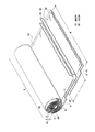
この電気二重層コンデンサ2は本発明のコンデンサの一例である。この電気二重層コンデンサ2には、図1に示すように、コンデンサ素子4の同一の素子端面に陽極部6と陰極部8が形成されている。陽極部6及び陰極部8は、電極張出し部の一例であって、コンデンサ素子4の素子端面から引き出された電極体(陽極体60又は陰極体80:図3)の一部で構成される。陽極部6と陽極端子10との接続には両者間に介在させた陽極集電板12が用いられ、また、陰極部8と陰極端子14との接続には両者間に介在させた陰極集電板16が用いられている。これらの接続には例えば、レーザ溶接や電子ビーム溶接が用いられ、18は溶接接続部の一例である。また、陽極端子10及び陰極端子14は外部接続のための端子部材であって、陽極端子10は陽極端子部材の一例、陰極端子14は陰極端子部材の一例である。この実施の形態では、陽極集電板12と接続された陽極部6及び陰極集電板16と接続された陰極部8の外周面には、絶縁手段17が設置されている。この絶縁手段17によってコンデンサ素子2と外装ケース20との絶縁が図られる。この絶縁手段17は例えば、絶縁紙や絶縁テープ等の絶縁材料を用いればよい。
The electric
コンデンサ素子4は円筒体であって、一方の素子端面に陽極体60(図3、図4)を引き出して陽極部6が形成されているとともに、陰極体80(図3)を引き出して陰極部8が形成されている。コンデンサ素子4の周囲には保持テープ19が巻回され、陽極体60や陰極体80の巻き戻りが防止されている。
コンデンサ素子4の外装部材として外装ケース20及び封口板22が備えられる。外装ケース20は例えばアルミニウム等の成形性のある金属材料からなる成形体である。封口板22は外装ケース20の開口部を閉止し、空間部24の気密性を保持する手段であるとともに、陽極端子10及び陰極端子14を固定する固定部材であり、コンデンサ素子4の支持部材を構成している。この実施の形態では、封口板22にベース部26と、封止部28とが備えられる。ベース部26は絶縁材料である例えば、合成樹脂で形成され、陽極端子10及び陰極端子14が固定されるとともに、絶縁されている。封止部28は密閉性の高い材料例えば、ゴム環で構成されている。
An
この封口板22は、外装ケース20の開口部30に挿入されるとともに、開口部30側の中途部に形成された加締め段部32に位置決めされている。外装ケース20の開口端部34は、カーリング処理により加締められ、封止部28に食い込ませられている。これらにより、外装ケース20が強固に封止されている。そして、封口板22のベース部26には、透孔36が形成されるとともに、薄ゴムからなる圧力開放機構38が形成されている。
The sealing
次に、コンデンサ素子4について、図3を参照する。図3は一部を分解して示したコンデンサ素子を示している。
Next, the
このコンデンサ素子4は、図3に示すように、陽極体60と、陰極体80と、セパレータ40、42とを備え、陽極体60と陰極体80との間には両者間を絶縁するセパレータ40、42のそれぞれが挟み込まれて巻回され、円筒状の巻回素子を構成している。陽極体60及び陰極体80にはベース材に例えば、アルミニウム箔が用いられ、このアルミニウム箔の両面に活性炭等の活物質及び結着剤等を含む分極性電極が形成されている。
As shown in FIG. 3, the
また、このコンデンサ素子4では、同一端面側に形成された陽極部6と陰極部8との間には一定幅の絶縁間隔44が設けられている。陽極部6は例えば、陽極体60の基材で形成され、同様に陰極部8も陰極体80の基材で形成されている。陽極体60及び陰極体80がアルミニウムで形成される場合、陽極部6及び陰極部8は、分極性電極を形成していないアルミニウム面を露出させた基材部である。
In the
陽極部6又は陰極部8の形成部は、絶縁手段であるセパレータ40、42の幅Wより突出する形態とし、各陽極部6又は陰極部8の円弧長に対応する長さLに形成されている。長さLを以て突出する各陽極部6及び陰極部8には、折り曲げ加工の準備加工として、素子端面5と平行で素子端面5から僅かに露出する位置に折り目線43が形成されている。この折り目線43は、各陽極部6及び陰極部8に対し、折り曲げ方向部を谷折りとする屈曲部である。
The formation part of the
そして、コンデンサ素子4の陽極部6又は陰極部8は、陽極集電板12又は陰極集電板16との接続前に、図2(又は図4のB)に示すように、加工してコンデンサ素子4の素子端面に密着状態に形成される。
Then, the
次に、コンデンサ素子の陽極部6及び陰極部8について、図4を参照する。図4はコンデンサ素子の陽極部及び陰極部の一例を示し、Aは陽極部及び陰極部の成形前、Bは陽極部及び陰極部の成形後を示している。図4において、図1、図2及び図3と同一部分には同一符号を付してある。
Next, FIG. 4 is referred with respect to the
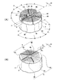
コンデンサ素子4の素子端面には図4のAに示すように、電極張出し部を構成する陽極部6と陰極部8とが立設され、これら陽極部6と陰極部8との間には所定幅の絶縁間隔44が設定されている。絶縁間隔44の中心にY軸、このY軸と直交方向にX軸を取り、X軸を中心に左右に角度θ1 、θ2 (>θ1 )を設定して区画する。角度θ1 でコンデンサ素子4の巻回中心部(巻芯部)46を中心に放射状方向に複数の切込み48を入れ、各切込み48で区画された複数の区画部6A、6B、6Cが陽極部6側に形成されている。同様に、複数の陰極部8側にも複数の区画部8A、8B、8Cが形成されている。角度θ1 を例えば、33〔°〕に設定すれば、区画部6A、8Aは2θ1 =66〔°〕となり、区画部6Aを挟んで形成された区画部6B、6C又は区画部8Aを挟んで形成された区画部8B、8Cの角度θ2 は、θ2 =57〔°〕に設定されている。
As shown in FIG. 4A, an
切込み48の深さは例えば、張出し長を陽極部6と陰極部8の高さh1 に設定され、陽極部6の区画部6A、6B、6C、陰極部8の区画部8A、8B、8Cを中途部で屈曲させ、コンデンサ素子4の素子中心部側に押し倒して圧縮成形することにより、図4のBに示すように、各区画部6A、6B、6C、陰極部8の区画部8A、8B、8Cに成形される。この実施の形態では、各区画部6B、6C及び区画部8B、8Cが溶接部分に設定されている。そこで、区画部6A、8Aの突出高さh2 が各区画部6B、6C、8B、8Cの高さh3 より高く設定され、区画部6A、6B、6C及び陰極部8の区画部8A、8B、8Cの高さを陽極集電板12及び陰極集電板16の屈曲形状に対応させている。
For example, the depth of the
なお、コンデンサ素子の陽極部6及び陰極部8は、このように素子中心方向に向かって陽極部6及び陰極部8全体を圧縮成形することで、高さ寸法を抑制できる。この実施の形態では、陽極部6の区画部6B、6Cを圧縮形成して、安定した平坦状の接続面を形成し、その後、非接続面である区画部6Aを圧縮成形し、各区画部間6A−6B、6A−6Cの重なりによって生じる境界部の高さ寸法を抑制している。この境界部の高さ寸法の抑制については陰極部8においても同様である。
In addition, the
次に、陽極集電板12(又は陰極集電板16)について、図5を参照する。図5は陽極集電板(又は陰極集電板)の一例を示し、Aはその平面、Bは陽極集電板を溶接接続部側から見た側面を示している。 Next, the anode current collecting plate 12 (or the cathode current collecting plate 16) will be described with reference to FIG. FIG. 5 shows an example of the anode current collector plate (or cathode current collector plate), A is a plane thereof, and B is a side view of the anode current collector plate as viewed from the weld connection portion side.
この陽極集電板12は電極材料と同一の例えば、アルミニウム板で形成され、既述の陽極部6の区画部6A、6B、6C(図4)を覆い、区画部6B、6Cとのレーザ溶接面積を持ち、且つ陽極端子10とのレーザ溶接面積を持つ形状及び面積を備えている。この実施の形態では、コンデンサ素子4の素子端面の2分の1の大きさであって、絶縁間隔44が確保される形状として、ほぼ半円形板である。
The anode
陽極集電板12には、図5のAに示すように、弦側中心部にコンデンサ素子4の巻回中心部46に対応して円弧状切欠部50が形成され、その弧側には、X軸を中心にX軸と直交方向に直線状に切り落とされた接続面部52が形成されている。また、この陽極集電板12には、図5のBに示すように、円弧状切欠部50を中心即ち、X軸を中心に左右に角度θ1 を持って直角に屈曲させた段部54を以て円弧状の端子接続部56A及び素子接続部56B、56Cが形成されている。各端子接続部56A及び素子接続部56B、56Cは、それぞれ平坦面に形成され、段部54を挟んで平行面を構成している。
As shown in FIG. 5A, the anode
この陽極集電板12において、端子接続部56Aの高さをh4 、陽極集電板12の厚さをt、端子接続部56Aの内側の高さをh5 とすると、
h5 =h4 −t≧h2 −h3 ・・・(1)
に設定されている。従って、端子接続部56Aの内側の高さをh5 は、区画部6A、8Aの突出高さh2 と各区画部6B、6C、8B、8Cの高さh3 との差分Δh(≧h2 −h3 )を吸収し、陽極集電板12が各区画部6B、6Cに密着し、且つ区画部6Aを収納して設置される。なお、陽極集電板12の厚さtは、端子接続部56B、56Cと端子接続部56Aの部位で厚さを変更することもできる。例えば、端子接続部56Aの厚みを端子接続部56B、56Cに比べて厚く設定(1.2倍以上)することができ、これによると陽極部6とのレーザ溶接の際に端子接続部56B、56Cに生じる発熱が所定厚みを有する端子接続部56Aによって吸収され、レーザ溶接の接続精度が向上する。
In the anode
h 5 = h 4 −t ≧ h 2 −h 3 (1)
Is set to Therefore, the inner height h 5 of the
このような構成及び他の部材との関係については、陰極集電板16についても同様である。
This configuration and the relationship with other members are the same for the cathode
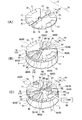
次に、陽極集電板12及び陰極集電板16と、コンデンサ素子4の陽極部6及び陰極部8との接続について、図6を参照する。図6はコンデンサ素子の素子端面上の陽極集電板及び陰極集電板の配置及び接続状態の一例を示している。
Next, FIG. 6 is referred to regarding the connection between the anode
陽極集電板12及び陰極集電板16は図6に示すように、コンデンサ素子4の一端面に巻回中心部46を中心にし、且つ巻回中心部46に円弧状切欠部50を合わせて配置され、陽極部6と陰極部8との間の絶縁間隔44に対応して間隔61が設定されている。陽極集電板12には、端子接続部56Aの下面側にコンデンサ素子4の陽極部6の区画部6A、陽極集電板12の素子接続部56B、56Cの下面側にコンデンサ素子4の陽極部6の区画部6B、6Cが位置決めされて密着させられる。そして、レーザ照射接続部66では、コンデンサ素子4の周縁方向から素子中心部方向に向かうレーザ照射により、区画部6B、6C及び素子接続部56B、56Cを部分的又は全面的に溶融させ、接続している。このような接続は陰極集電板16側でも同様である。
As shown in FIG. 6, the anode
レーザ照射の部位は、この実施の形態では、図6に示すように、陽極集電板12及び陰極集電板16の段部54で隔てた素子接続部56B、56Cの各2箇所即ち、レーザ照射接続部66である。この場合、レーザ照射接続部66に付した矢印〔1〕、〔2〕、〔3〕及び〔4〕で示すように、レーザ照射を行う。このレーザ照射は、シールドガスにアルゴンガス、ヘリウムガス等の不活性ガスを用いてコンデンサ素子4をシールドし、コンデンサ素子4に対するレーザ熱やスパッタの影響を回避する。
In this embodiment, as shown in FIG. 6, laser irradiation is performed at two portions of the
〔1〕このレーザ照射は、コンデンサ素子4の外周側より、素子中心方向に向かって直線状に一方の陽極集電板12の素子接続部56Bに照射する。
[1] This laser irradiation irradiates the
〔2〕次に、巻回中心部46を隔てて対向する他方の陰極集電板16の素子接続部58Bに素子中心側より、素子外周方向に向かって直線上にレーザ照射することにより、一連の動作にて溶接される。
[2] Next, a series of laser irradiation is performed in a straight line from the element center side toward the element outer peripheral direction to the
〔3〕また、同じく、レーザ照射は、コンデンサ素子4の外周側より、素子中心方向に向かって直線状に一方の陽極集電板12の素子接続部56Cに照射する。
[3] Similarly, laser irradiation is performed from the outer peripheral side of the
〔4〕そして、巻回中心部46を隔てて対向する他方の陰極集電板16の素子接続部58Cに素子中心側より素子外周側に向かって直線上にレーザを照射する一連の動作にて溶接される。
[4] In a series of operations of irradiating the
このように、巻回中心部46を隔てて直線状にレーザ照射する一連の動作にて、陽極部6と陽極集電板12、陰極部8と陰極集電板16とが接続される。つまり、陽極部6及び陰極部8と各集電板12、16とを巻回中心部46を隔ててコンデンサ素子4の直径方向に向かう溶接ライン(レーザ照射接続部66)を設定して溶接するので、陽極部6及び陰極部8と各集電板12、16との接続のための溶接の時間短縮を図ることができ、製造工程の簡略化を図ることができる。なお、レーザ照射の〔1〕及び〔2〕の一連の動作を2回繰り返す。又は、レーザ照射の〔1〕ないし〔4〕の一連の動作を2回繰り返し、近傍に溶接部を配することで接続抵抗を更に低減することも可能である。レーザ照射の〔1〕及び〔2〕の一連の動作にて接続することも可能であるが、陽極集電板12、陰極集電板16の各素子接続部56B、56C、58B、58Cを、それぞれ素子中心側より素子外周側に向かって直線上に照射する等、個別に接続することもできる。
In this way, the
また、レーザ照射の〔1〕ないし〔4〕の連続動作について、同一箇所を連続してレーザ照射するのではなく、レーザ溶接を〔1〕から〔4〕で行い、その後、再び〔1〕から〔4〕にレーザ照射すれば、同一箇所のレーザ照射に時間間隔を設けることができ、この結果、レーザ照射箇所の冷却化を図ることができ、レーザ溶接による接続の安定化が図られる。また、同一箇所に時間間隔を設けて複数回のレーザ照射を行うことも可能であるが、1回目のレーザ溶接を〔1〕から〔4〕で行い、再びレーザ溶接を〔1〕から〔4〕で行うので、冷却間隔を取りながら、レーザ照射を連続的に行うことができ、レーザ照射による溶接時間の短縮化を図ることができる。 In addition, in the continuous operation of laser irradiation [1] to [4], laser welding is performed from [1] to [4] instead of continuously irradiating the same part with laser, and then from [1] again. When the laser irradiation is performed in [4], a time interval can be provided for laser irradiation at the same location, and as a result, the laser irradiation location can be cooled and the connection by laser welding can be stabilized. It is also possible to perform laser irradiation a plurality of times with a time interval at the same location, but the first laser welding is performed from [1] to [4], and laser welding is performed again from [1] to [4]. Therefore, laser irradiation can be performed continuously while taking a cooling interval, and the welding time by laser irradiation can be shortened.
このレーザ照射の〔1〕ないし〔4〕の連続動作について、各レーザ照射の始点から終点に至る溶接ラインに対するレーザ出力を段階的又は連続的に減衰させるとよい。具体的には、レーザ出力を始点から終点にかけて3区間を設け、始点区間のレーザ出力Pa、中間区間のレーザ出力Pb、終点区間のレーザ出力Pcとし、レーザ出力をPa>Pb、Pb>Pcに減衰させている。始点区間のレーザ出力Paは最も高い値に設定され、一例として50〔W〕〜3000〔W〕である。レーザ出力Pbはレーザ出力Paの90〔%〕以下のレーザ出力とし、またレーザ出力Pcはレーザ出力Paの80%以下のレーザ出力としている。このように、各レーザ照射の始点から終点に至る溶接ラインに対するレーザ出力を段階的又は連続的に減衰させることで、集電板12、16、陽極部6及び陰極部8に加えられる溶接エネルギーを均一化でき、接続性を向上させることができ、安定した溶接接続を実現できる。即ち、レーザ照射を受けた陽極集電板12又は陰極集電板16及び陽極部6又は陰極部8の溶接ライン(レーザ照射接続部66)及びその近傍部が加熱され、レーザ照射を溶接ライン18に沿って行えば、レーザ照射の走査に応じて加熱がその走査とともに連鎖状態で移動するので、レーザ出力を同一に設定しなくても、連鎖的に溶融状態となる。このため、レーザ出力を段階的及び連続的に減衰させても、溶接部に加わるレーザ照射による熱エネルギーは均一化する。このため、陽極集電板12又は陰極集電板16と陽極部6又は陰極部8との接続性が向上する。
Regarding the continuous operations [1] to [4] of this laser irradiation, the laser output to the welding line from the start point to the end point of each laser irradiation may be attenuated stepwise or continuously. Specifically, three sections are provided from the start point to the end point of the laser output, and the laser output Pa of the start point section, the laser output Pb of the intermediate section, and the laser output Pc of the end point section are set, and the laser output satisfies Pa> Pb and Pb> Pc. It is attenuated. The laser output Pa in the start point section is set to the highest value, and is 50 [W] to 3000 [W] as an example. The laser output Pb is a laser output of 90% or less of the laser output Pa, and the laser output Pc is a laser output of 80% or less of the laser output Pa. In this way, the laser output to the welding line from the start point to the end point of each laser irradiation is attenuated stepwise or continuously, so that the welding energy applied to the
なお、図4に示すように、コンデンサ素子4の素子端面5には陽極部6及び陰極部8が形成されている。陽極部6及び陰極部8には、中心方向に向かって圧縮成形した際に、陽極部6及び陰極部8が接触しない絶縁間隔44を設定しており、このため、コンデンサ素子4の巻回中心部46近傍(素子中心部から2mm以内)では、陽極部6及び陰極部8が形成されていない。また、陽極部6及び陰極部8は、その形成部位が多いほど(又は面積が大きいほど)、抵抗の低減につながるため、陽極部6及び陰極部8が接触せず、また、低抵抗化が図れる絶縁間隔44として、例えば、3〔mm〕〜15〔mm〕を設定している。また、コンデンサ素子4の最外周では、陽極部6及び陰極部8の圧縮成形時にずれ等が生じても陽極部6及び陰極部8が外装ケース20に接触しないように、陽極集電板12と接続された陽極部6及び陰極集電板16と接続された陰極部8の外周面に絶縁紙や絶縁テープ等の絶縁手段17(図1)を設置すればよい。この絶縁手段17を、該陽極部6及び陰極部8に加え、陽極端子10、陰極端子14、陽極集電板12、陰極集電板16を覆うように外周に沿って設置すれば、外装ケース20との絶縁が図られる。
As shown in FIG. 4, an
次に、陽極端子10と陽極集電板12の接続、陰極端子14と陰極集電板16の接続について、図7を参照する。図7は陽極端子と陽極集電板、陰極端子と陽極集電板の接続を示し、Aは状態陽極端子と陽極集電板、陰極端子と陽極集電板の接続前の状態、Bはレーザ照射を示す図である。
Next, FIG. 7 will be referred to regarding the connection between the
陽極集電板12及び陰極集電板16が接続されたコンデンサ素子4には、図7に示すように、封口板22にある陽極端子10、陰極端子14が位置決めされる。陽極端子10及び陰極端子14には側面部に端子側接続面64が形成され、この端子側接続面64は、陽極集電板12及び陰極集電板16にある接続面部52と同一面を形成する側壁面である。そこで、これら接続面部52及び端子側接続面64を合致させ、レーザ照射68を行えば、既述の溶接接続部18がレーザ溶着され、接続面部52及び端子側接続面64間を溶着させることができる。
As shown in FIG. 7, the
従って、コンデンサ素子4の陽極部6には陽極集電板12を介して外部端子である陽極端子10がレーザ照射68による溶接接続部18を以て接続され、また、コンデンサ素子4の陰極部8には陰極集電板16を介して外部端子である陰極端子14がレーザ照射68による溶接接続部18を以て接続され、コンデンサ素子4に外部端子が形成される。
Therefore, the
ここで、コンデンサ素子4と封口板22との間隔(距離)を長く取ると、その分抵抗が増えてしまうとともに、電気二重層コンデンサ2の高さ寸法が大きくなってしまうため、コンデンサ素子4と封口板22との間隔(距離)を極力短くしている。このような小スペースにおいて、陽極端子10及び陰極端子14と、陽極集電板12及び陰極集電板16とを接続するために、既述の通り、接続面部52及び端子側接続面64を一致した共通の面部とし、この部位に局所的に溶接可能なレーザ照射にて溶接することで溶接の簡易化及び強化が図られている。ここで、陽極集電板12及び陰極集電板16、陽極端子10及び陰極端子14の厚み(接続面部52及び端子側接続面64の高さ寸法)は、それぞれ0.5〔mm〕〜5〔mm〕の範囲で設定されており、これによると、レーザ溶接が可能な寸法で且つ内部抵抗が増大され難く、また、電気二重層コンデンサ2の高さ寸法を短くすることができる。
Here, if the distance (distance) between the
また、接続面部52及び端子側接続面64は、レーザ照射の際に他の部材(陽極部6や陰極部8)への過剰なストレスを防ぐためにも、コンデンサ素子4の外周面近傍に設置されることが好ましく、具体的には、コンデンサ素子4の外周面より、例えば、10〔mm〕以内とすることが好ましい。
Further, the
また、陽極集電板12、陰極集電板16において、コンデンサ素子4の陽極部6及び陰極部8との接続領域と、陽極端子10と陰極端子14との接続領域とが異なる位置に設定されているので、各電極部と集電板、各外部端子と集電板との接続を安定化させることができ、コンデンサ素子の低抵抗化とともに接続の強化を図ることができる。
In the anode
以上説明した第1の実施の形態の電気二重層コンデンサ2の特徴事項や利点を列挙すれば以下の通りである。
The features and advantages of the electric
(1) コンデンサ素子4の一端面側に陽極体60の基材で陽極部6、陰極体80の基材で陰極部8が形成され、陽極部6と陽極端子10とが陽極集電板12を介して接続され、陰極部8と陰極端子14とが陰極集電板16を介して接続されるので、端子接続のシンプル化が図られている。しかも、接続を容易化することができる。
(1) On one end surface side of the
(2) 外装ケース20の空間部24内に接続部の占める空間専有率が極めて低い。
(2) The space occupation rate occupied by the connecting portion in the
(3) 外装部材である封口板22には、コンデンサ素子4が強固に支持されている。即ち、陽極端子10及び陰極端子14に陽極集電板12、陰極集電板16を介してコンデンサ素子4の陽極部6及び陰極部8のレーザ溶接により、強固に固定されるので、コンデンサ素子4の支持強度が高められている。この結果、機械的に堅牢な支持構造が構成され、製品の耐震性を高めることができる。
(3) The
(4) 巻回素子であるコンデンサ素子4に巻回されている陽極体60から複数の側縁部を集合させて陽極部6が形成され、この陽極部6を陽極集電板12にレーザ溶接し、同様に、陰極体80から複数の側縁部を集合させて陰極部8が形成され、この陰極部8を陰極集電板16にレーザ溶接しているので、コンデンサ素子4及び電気二重層コンデンサ2の低抵抗化を図ることができ、等価直列抵抗の低い製品を提供できる。
(4) A plurality of side edge portions are assembled from the
(5) 陽極集電板12及び陰極集電板16を用いたので、コンデンサ素子4にタブを接続する必要がない。
(5) Since the anode
(6) 陽極集電板12又は陰極集電板16と外部端子(陽極端子10又は陰極端子14)との側面の同一面化しているので、両者に対するレーザ照射を安定でき、接続の完全化及び信頼性を高めることができる。
(6) Since the side surfaces of the anode
(7) レーザ照射時にシールドガスを用いるので、レーザ熱や、飛翔するスパッタからコンデンサ素子4を防護でき、コンデンサ素子4及び製品であるコンデンサ2の特性劣化を防止でき、信頼性を向上させることができる。
(7) Since a shield gas is used during laser irradiation, the
〔第2の実施の形態〕 [Second Embodiment]
第2の実施の形態は、既述のコンデンサの製造方法について開示している。 The second embodiment discloses a method for manufacturing a capacitor as described above.
第2の実施の形態について、図8、図9及び図10を参照する。図8は、第2の実施の形態に係る電気二重層コンデンサの製造工程の一例を示すフローチャート、図9は陽極部及び陰極部の成形状態、図10は集電板とコンデンサ素子とのレーザ溶接工程を示している。 The second embodiment will be described with reference to FIG. 8, FIG. 9, and FIG. FIG. 8 is a flowchart showing an example of the manufacturing process of the electric double layer capacitor according to the second embodiment, FIG. 9 is a molding state of the anode part and the cathode part, and FIG. 10 is laser welding of the current collector plate and the capacitor element. The process is shown.
この製造工程は、本発明のコンデンサの製造方法の一例であって、図8に示すように、コンデンサ素子4及び電極部(電極張出し部)の形成工程(ステップS11)、陽極部6及び陰極部8の成形工程(ステップS12)、第1の接続工程(ステップS13)、第2の接続工程(ステップS14)、電解液含浸及び封止工程(ステップS15)を含んでいる。
This manufacturing process is an example of a method of manufacturing a capacitor according to the present invention. As shown in FIG. 8, the
(1) コンデンサ素子4及び電極部(電極張出し部)の形成工程(ステップS11)
(1)
図3に示すように、陽極体60及び陰極体80の間にセパレータ40、42を挟み込み、巻回中心部46を中心に円筒状に巻回することにより、コンデンサ素子4が形成される。このコンデンサ素子4には、素子端面側に陽極体60及び陰極体80の一部を張り出させ、電極張出し部としての陽極部6及び陰極部8が形成される。陽極部6及び陰極部8には絶縁間隔44が設定されている。
As shown in FIG. 3, the
(2) 陽極部6及び陰極部8の成形工程(ステップS12)
(2) Molding process of
この成形工程では、電極張出し部としての陽極部6及び陰極部8を図4のAに示すように、既述の区画部6A、6B、6C、8A、8B、8Cに区画し、図4のBに示すように、それぞれを巻回中心部46の方向に折曲げ、成形する(ステップS12)。その成形は、図9に示すように、陽極集電板12、陰極集電板16の屈曲形状に対応し、密着可能な高さに成形される。図9において、A及びBは陽極集電板12に接続される陽極部6の区画部6B、6C、陰極集電板16に接続される陰極部8の区画部8B、8Cの折曲げ状態(成形状態)を示し、Aは、後述する陽極集電板12及び陰極集電板16を設置する前の成形状態を示し、Bは陽極集電板12及び陰極集電板16を設置後の成形状態を示す。つまり、陽極集電板12及び陰極集電板16を陽極部6及び陰極部8に押し付けて、又は陽極部6及び陰極部8を陽極集電板12及び陰極集電板16に押し付けて圧縮することで、該陽極部6の区画部6B、6C及び陰極部8の区画部8B、8Cが平坦状となり、陽極集電板12、陰極集電板16に密着することになる。また、図3に示すように、陽極部6又は陰極部8を折り曲げ、成形する前に陽極部6又は陰極部8に予め折り目線43を設けても良い。折り目線43は、素子端面から一定の幅(0.5mm以上)の位置に形成されており、これにより陽極部6又は陰極部8の折り曲げ時に素子端面位置のセパレータ部位に加わる機械的ストレスが減少し、陽極体60、陰極体80の接触によるショート等を防止可能となる。なお、この折り目線43はキズではなくケガキ線であって、陽極部6及び陰極部8の折り曲げ時の座屈を防止することができる。この折り目線43は溝であり、断面形状は三角、四角又は湾曲(R)であってもよい。この折り目線43の形成には例えば、プレス、レーザ、切削等の方法を用いればよい。折り目線43は図3に示すように1本であってもよいが、陽極部6又は陰極部8の幅に応じて複数本としてもよい。折り目線43の形成面部は、陽極部6又は陰極部8の片面でもよいが、両面であってもよい。一例としての折り目線43は、素子端面の巻回中心部46に対向する面が谷折りになるように形成されている。
In this molding step, the
(3) 第1の接続工程(ステップS13) (3) 1st connection process (step S13)
この接続工程(ステップS13)では、図10のAに示すように、コンデンサ素子4の陽極部6に陽極集電板12、コンデンサ素子4の陰極部8に陰極集電板16を位置決めし、図10のBに示すように、陽極部6に陽極集電板12をまた、陰極部8に陰極集電板16をそれぞれレーザ溶接により接続する。このレーザ溶接では、アルゴンガス、ヘリウムガス等の不活性ガスをシールドガスに用いることにより、コンデンサ素子4をシールドし、レーザ熱や飛翔するスパッタからコンデンサ素子4を分離させる。
In this connection step (step S13), as shown in FIG. 10A, the anode
(4) 第2の接続工程(ステップS14) (4) Second connection process (step S14)
この接続工程(ステップS14)では、図7に示すように、陽極部6に接続された陽極集電板12に封口板22にある陽極端子10の接続面52と端子側接続面64とを同一面に合わせ、レーザ溶接により接続する。同様に、陰極部8に接続された陰極集電板16に封口板22の陰極端子14をレーザ溶接により接続する。このレーザ溶接においても、アルゴンガス、ヘリウムガス等の不活性ガスをシールドガスに用いることにより、コンデンサ素子4をシールドし、レーザ熱や飛翔するスパッタからコンデンサ素子4を分離させる。
In this connection step (step S14), as shown in FIG. 7, the anode
この実施の形態では、図7のAに示すように、コンデンサ素子4の陽極部6に接続された陽極集電板12に対して封口板22の陽極端子10を位置決めし、同時にコンデンサ素子4の陰極部8に接続された陰極集電板16に対して封口板22の陰極端子14を位置決めすることにより、図7のBに示すように、それぞれをレーザ溶接する。18は既述の溶接接続部である。
In this embodiment, as shown in FIG. 7A, the
なお、封口板22は陽極端子10及び陰極端子14のインサートにより合成樹脂を成形(インサート成形)し、これによりベース部26及び封止部28が形成される。
The sealing
(5) 電解液含浸及び封止工程(ステップS15) (5) Electrolyte impregnation and sealing process (step S15)
コンデンサ素子4は、電解液を含浸した後、外装ケース20に収容し、外装ケース20の開口端部34のカーリング処理により封止し(ステップS15)、製品である電気二重層コンデンサ2(図1)を完成する。
The
このような製造工程によれば、既述の電気二重層コンデンサ2を容易に製造でき、端子接続工程の簡略化を図ることができ、第1の実施の形態で述べた通りの効果を有するコンデンサを実現できる。
According to such a manufacturing process, the above-described electric
〔第3の実施の形態〕 [Third Embodiment]
第3の実施の形態では、外部端子の配置及び集電板の形態について開示する。 In the third embodiment, it discloses embodiments of the arrangement of the external terminals and the current collecting plate.
第3の実施の形態について、図11を参照する。図11は第3の実施の形態に係る集電板と外部端子との接続を示し、Aは接続前、Bは接続中のレーザ照射を示している。 The third embodiment will be described with reference to FIG. FIG. 11 shows the connection between the current collector plate and the external terminal according to the third embodiment. A shows the laser irradiation before the connection and B shows the laser irradiation during the connection.
この実施の形態の封口板22に設置された陽極端子10及び陰極端子14は、図11のAに示すように、コンデンサ素子4の素子端面の巻回中心部46に近接して配置されている。そして、陽極端子10及び陰極端子14の端子側接続面64は、コンデンサ素子4の外周面より巻回中心部46側に後退している。
As shown in FIG. 11A, the
このような陽極端子10、陰極端子14及び端子側接続面64に対し、この実施の形態では、図11のAに示すように、陽極集電板12及び陰極集電板16の端子接続部56A、58Aに巻回中心部46側に後退した凹部70が形成されている。この凹部70には陽極端子10又は陰極端子14の端子側接続面64に対応して既述の接続面部52が形成されている。この場合、陽極集電板12又は陰極集電板16では、端子側接続面64の側面部に対し素子接続部56B、56Cは、コンデンサ素子の外周方向に突出する平坦部を構成している。
In this embodiment, as shown in FIG. 11A, the
このような構成とすれば、図11のAに示すように、コンデンサ素子4の素子端面の巻回中心部46に近接して陽極端子10や陰極端子14が配置されていても、端子側接続面64及び接続面52を同一面に維持し、上記実施の形態と同様のレーザ照射68による接続を行うことができる。
With such a configuration, as shown in FIG. 11A, even if the
なお、この実施の形態では、陽極集電板12及び陰極集電板16に凹部70を形成しているが、凸部を以て接続面52を形成してもよい。
In this embodiment, the
〔第4の実施の形態〕 [Fourth Embodiment]
第4の実施の形態では、集電板の他の形態について開示する。 In the fourth embodiment, another form of the current collector plate is disclosed.
第4の実施の形態について、図12を参照する。図12は第4の実施の形態に係る集電板、集電板と外部端子との接続を示し、Aは接続前の集電板、Bは接続前、Cは接続中のレーザ照射を示している。 FIG. 12 is referred to regarding the fourth embodiment. FIG. 12 shows the current collector plate according to the fourth embodiment, the connection between the current collector plate and the external terminal, A is the current collector plate before connection, B is before connection, and C is the laser irradiation during connection. ing.
この実施の形態の集電板12、16は、図12のAに示すように、間隔61を設けてコンデンサ素子4の素子端面5を覆う形態であり、第1の実施の形態と同様に裏面側には区画部6A、8Aを収納させる凹部69が形成されている。この集電板12、16の表面部には、コンデンサ素子4の区画部6A、8Aとの接続部分を扇形の突部71とし、この突部71を挟んで、コンデンサ素子4の区画部6B、6C、8B、8Cに対応する凹部73、75が形成されている。凹部73、75が外部端子との接続部よりコンデンサ素子2の外周方向に突出する平坦部を構成する。突部71には、周縁側に切欠部77が形成され、この切欠部77に臨む周縁部を円弧状に形成して陽極端子10又は陰極端子14との接続面79が形成されている。凹部73、75側には集電板12、16を同時に把持(チャッキング)する手段として、直方体状の突起部81が形成されている。
As shown in FIG. 12A, the
この実施の形態の集電板12、16は、図12のBに示すように、コンデンサ素子4の素子端面5を覆って設置され、陽極部6と集電板12の凹部73、75とがレーザ溶接により接続され、同様に陰極部8と集電板16の凹部73、75とがレーザ溶接により接続される。
As shown in FIG. 12B, the
そして、図12のCに示すように、コンデンサ素子4に接続された集電板12には陽極端子10が重ねられ、集電板16には陰極端子14が重ねられ、陽極端子10の接続面64と同一曲面を持つ接続面79を合致させ、同様に陰極端子14の曲面部と同一曲面を持つ接続面79を合致させて位置決めする。この位置決め状態により、レーザ照射68を行うことにより各集電板12、16と陽極端子10又は陰極端子14とを接続する。凹部73、75は、突部71にある。陽極端子10又は陰極端子14に接続される接続面79即ち、端子部材と溶接された側面部より集電板12、16の外周方向に突出する平坦部を構成している。この平坦部でコンデンサ素子4の素子端面5を被覆することができる。
Then, as shown in FIG. 12C, the
斯かる構成では、コンデンサ素子4の素子端面5が集電板12、16で覆われており、接続面79側のレーザ照射68によるスパッタの飛翔からコンデンサ素子4の素子端面5を防護できる。しかも、接続面79は、陽極端子10、陰極端子14の曲面に合致した曲面としているので、接続面79を陽極端子10、陰極端子14の接続面64に合致させて溶接を行うことができる。つまり、良好なレーザ溶接が行える。
In such a configuration, the
〔第5の実施の形態〕 [Fifth Embodiment]
第5の実施の形態は、封口板、外部端子又は集電板の何れかに位置決め手段を設け、位置決め手段で外部端子と集電板との接続位置を決定することを開示している。 The fifth embodiment discloses that positioning means is provided on any one of the sealing plate, the external terminal, and the current collecting plate, and the connection position between the external terminal and the current collecting plate is determined by the positioning means.
第5の実施の形態について、図13を参照する。図13は第4の実施の形態に係る封口板を示し、Aは背面側から見た封口板、Bは封口板で位置決めされた陽極集電板及び陰極集電板を示している。 A fifth embodiment will be described with reference to FIG. FIG. 13 shows a sealing plate according to the fourth embodiment, in which A shows a sealing plate viewed from the back side, and B shows an anode current collecting plate and a cathode current collecting plate positioned by the sealing plate.
この実施の形態の封口板22の背面側には、図13のAに示すように、陽極端子10及び陰極端子14との間にある空間部に絶縁材料からなる位置決め凸部72が形成され、この位置決め凸部72をコンデンサ素子4(図1)の巻回中心部46に向けて突出させている。この位置決め凸部72は、円柱状部74と、一対の平板状立壁部76とを備えている。円柱状部74は、陽極集電板12と陰極集電板16のそれぞれの円弧状切欠部50の円弧に対応する柱体部である。平板状立壁部76は、円柱状部74を備え、この円柱状部74を中心に陽極集電板12及び陰極集電板16の間隔61を維持する平板状立壁部76を左右に備えている。
On the back side of the sealing
このような位置決め凸部72を備えた封口板22を備えれば、位置決め凸部72で陽極集電板12及び陰極集電板16を所定位置に位置決めし、間隔61を所定幅wに維持することができる。即ち、位置決め凸部72の円柱状部74では陽極集電板12及び陰極集電板16の円弧状切欠部50を嵌合させ、各平板状立壁部76の側面に各陽極集電板12及び陰極集電板16を接することにより、陽極集電板12及び陰極集電板16が所定位置に位置決めされる。この位置決めにより、陽極端子10の端子側接続面64と陽極集電板12の接続面52、陰極端子14の端子側接続面64と陰極集電板16の接続面52をそれぞれ一致させることができ、レーザ照射による接続の安定化を図り、接続精度を高めることができるとともに、位置決め凸部72によって、陽極部6及び陰極部8が確実に絶縁隔離される。
If Sonaere the sealing
なお、この実施の形態では、封口板22側に位置決め凸部72を形成したが、外部端子(陽極端子10、陰極端子14)又は集電板(陽極集電板12及び陰極集電板16)の何れかに位置決め手段を設けてもよい。斯かる構成によっても、位置決め手段で外部端子と集電板との接続位置を決めることができ、レーザ照射面を画一的に同一化でき、接続の安定化を図り、信頼性の高い接続を実現できる。
In this embodiment, the
〔第6の実施の形態〕 [Sixth Embodiment]
第6の実施の形態は、集電板とは別に接続板を備えることを開示している。 The sixth embodiment discloses that a connection plate is provided separately from the current collector plate.
第6の実施の形態について、図14を参照する。図14は第6の実施の形態に係る電気二重層コンデンサを示している。 FIG. 14 is referred to for the sixth embodiment. FIG. 14 shows an electric double layer capacitor according to a sixth embodiment.
この第6の実施の形態では、図14に示すように、陽極端子部材として陽極端子10とともに陽極接続板88、陰極端子部材として陰極端子14とともに陰極接続板90を備えた構成である。陽極接続板88は陽極端子10にレーザ溶接により接続された後、コンデンサ素子4側の陽極集電板12に接続される。同様に、陰極接続板90は陰極端子14にレーザ溶接により接続された後、コンデンサ素子4側の陰極集電板16に接続される。陽極接続板88には陽極端子10を位置決めして接続する接続用凹部92、陰極接続板90には陰極端子14を位置決めして接続する接続用凹部94が形成されている。また、陽極接続板88及び陰極接続板90の周面の一部には、陽極集電板12又は陰極集電板16の接続面52に対応する接続面部96が形成され、この接続面部96と接続面52とが同一面をなし、レーザ溶接が施されて電気的に接続される。
In the sixth embodiment, as shown in FIG. 14, the
このような陽極接続板78及び陰極接続板80を用いた構成では、外部端子である陽極端子10、陰極端子14と、コンデンサ素子4側に接続された陽極集電板12、陰極集電板16との接続が広範囲に行われ、接続抵抗を低減でき、しかも接続強度を高めることができる。
In such a configuration using the anode connection plate 78 and the
〔他の実施の形態〕 [Other Embodiments]
(1) 上記実施の形態では、コンデンサ素子として巻回素子を例示したが、巻回素子に限定されない。積層型素子や固体素子であってもよい。 (1) In the embodiment described above, the winding element is exemplified as the capacitor element, but is not limited to the winding element. A multilayer element or a solid element may be used.
(2) 上記実施の形態では、コンデンサ素子の素子端面の一方(同一面)に陽極部6及び陰極部8を備えて外部端子に接続する構成を開示しているが、一方の素子端面に陽極部、他方の素子端面に陰極部を備える構成としてもよい。
(2) The above embodiment discloses a configuration in which the
(3) 上記実施の形態では、電気二重層コンデンサ2を例示したが、本発明はこれに限定されない。同一の構造及び方法は、電解コンデンサにも同様に適用でき、同様の効果が得られる。
(3) In the above embodiment, the electric
(4) 上記実施の形態では、集電板として陽極集電板12、陰極集電板16を例示したが、本発明は上記実施の形態に限定されない。接続面52は、フラット面としたが、外部端子の形状に合致する形状として、曲面であってもよい。この接続面52の位置についても、集電板の面内又は周面の何れでもよいし、接続用凸部を設けてもよい。
(4) In the above embodiment, the anode
(5) 上記実施の形態では、陽極部と陰極部との間に絶縁間隔を設置しているが、この絶縁間隔に絶縁部材を設置してもよい。 (5) In the above embodiment, an insulation interval is provided between the anode part and the cathode part, but an insulation member may be provided at this insulation interval.
(6) 上記実施の形態では、溶接手段として、レーザ溶接や電子ビーム溶接を例示したが、本発明はこれに限定されない。アーク溶接等を用いることもできる。この場合は、集電板の外周面側を凸状として接続面52を形成し、該接続面52と端子接続面64をアーク溶接すればよい。
(6) In the above embodiment, laser welding and electron beam welding are exemplified as the welding means, but the present invention is not limited to this. Arc welding or the like can also be used. In this case, the
(7) 上記実施の形態では、陽極部6及び陰極部8を半円形状に形成したが、本発明はこれに限定されない。実施の形態で示した陽極部6の区画部6A、6B、6C、陰極部8の区画部8A、8B、8Cのうち、陽極集電板12と陰極集電板16と接続する区画部6B、6C及び8B、8Cのみ張り出して形成し、陽極部の6A及び陰極部の8Aは張り出さなくてもよい。
(7) In the above embodiment, the
(8) 上記実施の形態では、集電板の異なる位置として3分割された区分により、陽極部6及び陰極部10との素子接続領域である区画部12B、12C又は16Bと、16C、端子接続領域である区画部12A又は16Aとが集電板の表裏面に設定され、水平方向に異なる位置に設定しているが、これに限定されない。集電板の一部に素子接続領域(レーザ照射接続部66)を設定し、その他の部位に端子接続領域(溶接接続部18)を設定してもよい。即ち、集電板の表裏面で溶接位置が異なれば、素子接続領域と端子接続領域が近接していてもよい。つまり、素子接続領域である区画部12Bにおいてレーザ照射接続部66と集電板の表裏面で溶接位置が重ならない部位に溶接接続部18を設定してもよい。
(8) In the above embodiment, the section 12B, 12C or 16B, which is the element connection area between the
以上説明したように、本発明の最も好ましい実施の形態等について説明したが、本発明は、上記記載に限定されるものではなく、特許請求の範囲に記載され、又は発明を実施するための形態に開示された発明の要旨に基づき、当業者において様々な変形や変更が可能であることは勿論であり、斯かる変形や変更が、本発明の範囲に含まれることは言うまでもない。
As described above, the most preferable embodiment and the like of the present invention have been described. However, the present invention is not limited to the above description, and is described in the claims or a form for carrying out the invention. It goes without saying that various modifications and changes can be made by those skilled in the art based on the gist of the invention disclosed in the above, and such modifications and changes are included in the scope of the present invention.
本発明のコンデンサ及びその製造方法は、端子接続構造や接続工程の簡略化に寄与し、生産性や信頼性を高めることができ、有益である。
The capacitor and the method for manufacturing the same according to the present invention contribute to simplification of the terminal connection structure and the connection process, and can increase productivity and reliability, which is beneficial.
2 電気二重層コンデンサ
4 コンデンサ素子
6 陽極部
60 陽極体
8 陰極部
80 陰極体
10 陽極端子
12 陽極集電板
14 陰極端子
16 陰極集電板
18 溶接接続部
19 保持テープ
20 外装ケース
22 封口板
24 空間部
26 ベース部
28 封止部
32 加締め段部
34 開口端部
36 透孔
38 圧力開放機構
44 絶縁間隔
2 Electric
Claims (10)
前記コンデンサ素子を収容するケース部材の開口部を封口する封口部材と、
前記コンデンサ素子の素子端面に前記電極体の何れか一方又は双方から張り出させた単一又は複数の電極張出し部と、
前記電極張出し部に接続された単一又は複数の集電板と、
前記封口部材に設置され、前記集電板に重ねられるとともに側面部が前記集電板の側面部に溶接された端子部材と、
を備え、前記端子部材の前記側面部が前記集電板の側面部と共通の面部を成すことを特徴とするコンデンサ。 Capacitor element which is a winding element or a non-winding element provided with an electrode body on the anode side and a cathode side, and a separator interposed between these electrode bodies,
A sealing member that seals the opening of the case member that houses the capacitor element;
A single or a plurality of electrode overhang portions projecting from either one or both of the electrode bodies on the element end face of the capacitor element;
A single or a plurality of current collectors connected to the electrode overhang, and
A terminal member that is installed on the sealing member, overlapped with the current collector plate, and a side surface portion welded to the side surface portion of the current collector plate ;
And the side surface portion of the terminal member forms a common surface portion with the side surface portion of the current collector plate .
前記コンデンサ素子の前記素子端面に形成された単一又は複数の電極張出し部の一部又は全部に形成された単一又は複数の溶接面部と溶接される単一又は複数の第1の溶接面部と、
前記第1の溶接面部と交差する側面部に設けられ、前記端子部材と溶接される第2の溶接面部と、
を備えることを特徴とする請求項1、2、3、4又は5の何れかに記載のコンデンサ。 The current collector plate is
A single or a plurality of first welding surfaces to be welded to a single or a plurality of welding surfaces formed on a part or all of the single or a plurality of electrode projections formed on the element end face of the capacitor element; ,
A second welding surface portion provided on a side surface intersecting with the first welding surface portion and welded to the terminal member;
Capacitor according to any one of claims 1, 2, 3, 4 or 5, characterized in that it comprises a.
前記素子端面上に前記区画部を以て形成された単一又は複数の溶接面部と、
を備えることを特徴とする請求項1、2、3、4、5又は6の何れかに記載のコンデンサ。 The electrode extension portion is partitioned at a predetermined angle around the element center portion of the element end surface, and a plurality of partition portions bent in the center direction of the element end surface with the same or different bending angles;
A single or a plurality of welding surface portions formed with the partition portion on the element end surface; and
Capacitor according to any one of claims 2, 3, 4, 5 or 6, characterized in that it comprises a.
前記コンデンサ素子を収容するケース部材の開口部を封口する封口部材に設置された端子部材と、前記電極張出し部に接続されている単一又は複数の集電板とを重ね、前記端子部材の側面部と前記集電板の側面部とを溶接する工程と、
を含み、前記端子部材の前記側面部に前記集電板の側面部を位置決めし、前記側面部間を共通面部として前記溶接を施すことを特徴とするコンデンサの製造方法。 The electrode body is protruded from the element end face of a capacitor element which is a winding element or a non-winding element provided with an anode-side and cathode-side electrode body and a separator interposed between the electrode bodies, Forming a single or a plurality of electrode overhangs;
A terminal member installed on a sealing member that seals an opening of a case member that accommodates the capacitor element, and a single or a plurality of current collector plates connected to the electrode overhanging portion are overlapped, and a side surface of the terminal member Welding a portion and a side portion of the current collector plate;
Only including the positioning of the side portion of the current collector plate to said side surface portion of the terminal member, a manufacturing method of a capacitor, characterized in that performing the welding between the side portion as a common surface.
Priority Applications (9)
| Application Number | Priority Date | Filing Date | Title |
|---|---|---|---|
| JP2010251352A JP5764912B2 (en) | 2010-11-09 | 2010-11-09 | Capacitor and manufacturing method thereof |
| PCT/JP2011/004623 WO2012023289A1 (en) | 2010-08-18 | 2011-08-18 | Capacitor, and method and program for manufacturing same |
| EP11817938.1A EP2608230B1 (en) | 2010-08-18 | 2011-08-18 | Capacitor, and method and program for manufacturing same |
| KR1020137006759A KR101930095B1 (en) | 2010-08-18 | 2011-08-18 | Capacitor, and method and program for manufacturing same |
| CN201180039963.7A CN103081047B (en) | 2010-08-18 | 2011-08-18 | Capacitor, the manufacture method of capacitor and fabrication schedule |
| PCT/JP2011/006266 WO2012063486A1 (en) | 2010-11-09 | 2011-11-09 | Capacitor and process for production thereof |
| CN201180053897.9A CN103210459B (en) | 2010-11-09 | 2011-11-09 | Capacitor and manufacture method thereof |
| US13/768,851 US9053858B2 (en) | 2010-08-18 | 2013-02-15 | Capacitor, and manufacturing method and manufacturing program thereof |
| US13/890,426 US9672985B2 (en) | 2010-11-09 | 2013-05-09 | Capacitor and method for manufacturing the same |
Applications Claiming Priority (1)
| Application Number | Priority Date | Filing Date | Title |
|---|---|---|---|
| JP2010251352A JP5764912B2 (en) | 2010-11-09 | 2010-11-09 | Capacitor and manufacturing method thereof |
Related Child Applications (1)
| Application Number | Title | Priority Date | Filing Date |
|---|---|---|---|
| JP2015121899A Division JP6112144B2 (en) | 2015-06-17 | 2015-06-17 | Capacitor and manufacturing method thereof |
Publications (3)
| Publication Number | Publication Date |
|---|---|
| JP2012104617A JP2012104617A (en) | 2012-05-31 |
| JP2012104617A5 JP2012104617A5 (en) | 2013-12-19 |
| JP5764912B2 true JP5764912B2 (en) | 2015-08-19 |
Family
ID=46394682
Family Applications (1)
| Application Number | Title | Priority Date | Filing Date |
|---|---|---|---|
| JP2010251352A Active JP5764912B2 (en) | 2010-08-18 | 2010-11-09 | Capacitor and manufacturing method thereof |
Country Status (1)
| Country | Link |
|---|---|
| JP (1) | JP5764912B2 (en) |
Families Citing this family (2)
| Publication number | Priority date | Publication date | Assignee | Title |
|---|---|---|---|---|
| WO2012063486A1 (en) | 2010-11-09 | 2012-05-18 | 日本ケミコン株式会社 | Capacitor and process for production thereof |
| JP6070552B2 (en) | 2011-06-28 | 2017-02-01 | 日本ケミコン株式会社 | Method for manufacturing power storage device |
Family Cites Families (4)
| Publication number | Priority date | Publication date | Assignee | Title |
|---|---|---|---|---|
| JPH11251190A (en) * | 1997-12-22 | 1999-09-17 | Asahi Glass Co Ltd | Electric double layer capacitor |
| JP2001068379A (en) * | 1999-08-24 | 2001-03-16 | Honda Motor Co Ltd | Electric double layer capacitor |
| JP2009188095A (en) * | 2008-02-05 | 2009-08-20 | Honda Motor Co Ltd | Storage capacitor connection structure |
| JP2010093178A (en) * | 2008-10-10 | 2010-04-22 | Panasonic Corp | Electrochemical capacitance and method of manufacturing the same |
-
2010
- 2010-11-09 JP JP2010251352A patent/JP5764912B2/en active Active
Also Published As
| Publication number | Publication date |
|---|---|
| JP2012104617A (en) | 2012-05-31 |
Similar Documents
| Publication | Publication Date | Title |
|---|---|---|
| JP6264431B2 (en) | Power storage device | |
| WO2012063486A1 (en) | Capacitor and process for production thereof | |
| JP2006252890A (en) | Cylinder-shaped secondary battery and manufacturing method of the same | |
| WO2018074135A1 (en) | Power storage device and power storage device production method | |
| JP5961940B2 (en) | Capacitor manufacturing method | |
| JP5961939B2 (en) | Capacitor manufacturing method | |
| JP5482565B2 (en) | Capacitor and manufacturing method thereof | |
| JP5764912B2 (en) | Capacitor and manufacturing method thereof | |
| JP5979273B2 (en) | Capacitor manufacturing method | |
| JP2012160658A (en) | Method of manufacturing capacitor | |
| US8574756B1 (en) | Prismatic secondary battery | |
| JP2012104618A (en) | Capacitor and manufacturing method thereof | |
| JP2012104622A (en) | Capacitor and manufacturing method thereof | |
| JP5928993B2 (en) | Capacitor manufacturing method | |
| CN108808011B (en) | Secondary battery and current collecting terminal | |
| JP5866753B2 (en) | Capacitor and manufacturing method thereof | |
| JP6112144B2 (en) | Capacitor and manufacturing method thereof | |
| JP2012104621A (en) | Capacitor and manufacturing method thereof | |
| JP2012104620A (en) | Capacitor and manufacturing method thereof | |
| JP5834617B2 (en) | Capacitor manufacturing method | |
| JP5866772B2 (en) | Capacitor and its terminal connection method | |
| JP2013191842A (en) | Capacitor and method of manufacturing the same | |
| JP5716851B2 (en) | Capacitor manufacturing method | |
| JP6364972B2 (en) | Power storage device and method for manufacturing power storage device | |
| JP2012059863A (en) | Power storage element |
Legal Events
| Date | Code | Title | Description |
|---|---|---|---|
| A521 | Written amendment |
Free format text: JAPANESE INTERMEDIATE CODE: A523 Effective date: 20131101 |
|
| A621 | Written request for application examination |
Free format text: JAPANESE INTERMEDIATE CODE: A621 Effective date: 20131101 |
|
| A131 | Notification of reasons for refusal |
Free format text: JAPANESE INTERMEDIATE CODE: A131 Effective date: 20140902 |
|
| A521 | Written amendment |
Free format text: JAPANESE INTERMEDIATE CODE: A523 Effective date: 20141104 |
|
| TRDD | Decision of grant or rejection written | ||
| A01 | Written decision to grant a patent or to grant a registration (utility model) |
Free format text: JAPANESE INTERMEDIATE CODE: A01 Effective date: 20150519 |
|
| A61 | First payment of annual fees (during grant procedure) |
Free format text: JAPANESE INTERMEDIATE CODE: A61 Effective date: 20150601 |
|
| R150 | Certificate of patent or registration of utility model |
Ref document number: 5764912 Country of ref document: JP Free format text: JAPANESE INTERMEDIATE CODE: R150 |