JP5757163B2 - Multilayer wiring board, manufacturing method thereof, and semiconductor device - Google Patents
Multilayer wiring board, manufacturing method thereof, and semiconductor device Download PDFInfo
- Publication number
- JP5757163B2 JP5757163B2 JP2011124604A JP2011124604A JP5757163B2 JP 5757163 B2 JP5757163 B2 JP 5757163B2 JP 2011124604 A JP2011124604 A JP 2011124604A JP 2011124604 A JP2011124604 A JP 2011124604A JP 5757163 B2 JP5757163 B2 JP 5757163B2
- Authority
- JP
- Japan
- Prior art keywords
- layer
- dielectric layer
- forming
- conductive layer
- metal foil
- Prior art date
- Legal status (The legal status is an assumption and is not a legal conclusion. Google has not performed a legal analysis and makes no representation as to the accuracy of the status listed.)
- Expired - Fee Related
Links
- 238000004519 manufacturing process Methods 0.000 title claims description 67
- 239000004065 semiconductor Substances 0.000 title description 18
- 239000011888 foil Substances 0.000 claims description 177
- 229910052751 metal Inorganic materials 0.000 claims description 175
- 239000002184 metal Substances 0.000 claims description 175
- 239000003990 capacitor Substances 0.000 claims description 151
- 239000010409 thin film Substances 0.000 claims description 137
- 238000000034 method Methods 0.000 claims description 117
- 230000008569 process Effects 0.000 claims description 91
- 239000004020 conductor Substances 0.000 claims description 80
- 230000002093 peripheral effect Effects 0.000 claims description 50
- 230000002542 deteriorative effect Effects 0.000 claims description 19
- 238000010030 laminating Methods 0.000 claims description 19
- 238000004873 anchoring Methods 0.000 claims description 13
- 238000007788 roughening Methods 0.000 claims description 3
- 239000000126 substance Substances 0.000 claims description 3
- 239000000758 substrate Substances 0.000 description 35
- 238000005530 etching Methods 0.000 description 18
- 239000011347 resin Substances 0.000 description 18
- 229920005989 resin Polymers 0.000 description 18
- 230000004048 modification Effects 0.000 description 17
- 238000012986 modification Methods 0.000 description 17
- 230000000694 effects Effects 0.000 description 15
- 230000003746 surface roughness Effects 0.000 description 13
- PXHVJJICTQNCMI-UHFFFAOYSA-N Nickel Chemical compound [Ni] PXHVJJICTQNCMI-UHFFFAOYSA-N 0.000 description 11
- 239000000463 material Substances 0.000 description 11
- 238000005498 polishing Methods 0.000 description 11
- 239000000470 constituent Substances 0.000 description 9
- 230000006866 deterioration Effects 0.000 description 7
- 230000032798 delamination Effects 0.000 description 6
- 239000010408 film Substances 0.000 description 6
- RYGMFSIKBFXOCR-UHFFFAOYSA-N Copper Chemical compound [Cu] RYGMFSIKBFXOCR-UHFFFAOYSA-N 0.000 description 5
- 238000005520 cutting process Methods 0.000 description 5
- 238000010586 diagram Methods 0.000 description 5
- 230000015556 catabolic process Effects 0.000 description 4
- 239000010949 copper Substances 0.000 description 4
- 230000003071 parasitic effect Effects 0.000 description 4
- 229910002113 barium titanate Inorganic materials 0.000 description 3
- 239000011889 copper foil Substances 0.000 description 3
- 239000000945 filler Substances 0.000 description 3
- 230000035939 shock Effects 0.000 description 3
- 229910000679 solder Inorganic materials 0.000 description 3
- 238000004544 sputter deposition Methods 0.000 description 3
- VEALVRVVWBQVSL-UHFFFAOYSA-N strontium titanate Chemical compound [Sr+2].[O-][Ti]([O-])=O VEALVRVVWBQVSL-UHFFFAOYSA-N 0.000 description 3
- 238000007740 vapor deposition Methods 0.000 description 3
- 230000002411 adverse Effects 0.000 description 2
- 229910052454 barium strontium titanate Inorganic materials 0.000 description 2
- JRPBQTZRNDNNOP-UHFFFAOYSA-N barium titanate Chemical compound [Ba+2].[Ba+2].[O-][Ti]([O-])([O-])[O-] JRPBQTZRNDNNOP-UHFFFAOYSA-N 0.000 description 2
- 238000000576 coating method Methods 0.000 description 2
- 229910052802 copper Inorganic materials 0.000 description 2
- 238000005553 drilling Methods 0.000 description 2
- 238000000059 patterning Methods 0.000 description 2
- 238000007747 plating Methods 0.000 description 2
- 230000009467 reduction Effects 0.000 description 2
- 238000004904 shortening Methods 0.000 description 2
- 229910015801 BaSrTiO Inorganic materials 0.000 description 1
- 229910002367 SrTiO Inorganic materials 0.000 description 1
- WOIHABYNKOEWFG-UHFFFAOYSA-N [Sr].[Ba] Chemical compound [Sr].[Ba] WOIHABYNKOEWFG-UHFFFAOYSA-N 0.000 description 1
- 230000008901 benefit Effects 0.000 description 1
- 239000011230 binding agent Substances 0.000 description 1
- 230000008859 change Effects 0.000 description 1
- 239000011248 coating agent Substances 0.000 description 1
- 238000006731 degradation reaction Methods 0.000 description 1
- 238000009499 grossing Methods 0.000 description 1
- 230000006872 improvement Effects 0.000 description 1
- 238000000465 moulding Methods 0.000 description 1
- 229910052759 nickel Inorganic materials 0.000 description 1
- 229920002120 photoresistant polymer Polymers 0.000 description 1
- 230000001681 protective effect Effects 0.000 description 1
- 238000003980 solgel method Methods 0.000 description 1
- 238000001039 wet etching Methods 0.000 description 1
Images


Classifications
-
- H—ELECTRICITY
- H01—ELECTRIC ELEMENTS
- H01G—CAPACITORS; CAPACITORS, RECTIFIERS, DETECTORS, SWITCHING DEVICES OR LIGHT-SENSITIVE DEVICES, OF THE ELECTROLYTIC TYPE
- H01G4/00—Fixed capacitors; Processes of their manufacture
- H01G4/002—Details
- H01G4/005—Electrodes
-
- H—ELECTRICITY
- H01—ELECTRIC ELEMENTS
- H01G—CAPACITORS; CAPACITORS, RECTIFIERS, DETECTORS, SWITCHING DEVICES OR LIGHT-SENSITIVE DEVICES, OF THE ELECTROLYTIC TYPE
- H01G4/00—Fixed capacitors; Processes of their manufacture
- H01G4/33—Thin- or thick-film capacitors
-
- H—ELECTRICITY
- H01—ELECTRIC ELEMENTS
- H01L—SEMICONDUCTOR DEVICES NOT COVERED BY CLASS H10
- H01L21/00—Processes or apparatus adapted for the manufacture or treatment of semiconductor or solid state devices or of parts thereof
- H01L21/02—Manufacture or treatment of semiconductor devices or of parts thereof
- H01L21/04—Manufacture or treatment of semiconductor devices or of parts thereof the devices having at least one potential-jump barrier or surface barrier, e.g. PN junction, depletion layer or carrier concentration layer
- H01L21/48—Manufacture or treatment of parts, e.g. containers, prior to assembly of the devices, using processes not provided for in a single one of the subgroups H01L21/06 - H01L21/326
- H01L21/4814—Conductive parts
- H01L21/4846—Leads on or in insulating or insulated substrates, e.g. metallisation
- H01L21/4857—Multilayer substrates
-
- H—ELECTRICITY
- H01—ELECTRIC ELEMENTS
- H01L—SEMICONDUCTOR DEVICES NOT COVERED BY CLASS H10
- H01L23/00—Details of semiconductor or other solid state devices
- H01L23/48—Arrangements for conducting electric current to or from the solid state body in operation, e.g. leads, terminal arrangements ; Selection of materials therefor
- H01L23/488—Arrangements for conducting electric current to or from the solid state body in operation, e.g. leads, terminal arrangements ; Selection of materials therefor consisting of soldered or bonded constructions
- H01L23/498—Leads, i.e. metallisations or lead-frames on insulating substrates, e.g. chip carriers
- H01L23/49805—Leads, i.e. metallisations or lead-frames on insulating substrates, e.g. chip carriers the leads being also applied on the sidewalls or the bottom of the substrate, e.g. leadless packages for surface mounting
-
- H—ELECTRICITY
- H01—ELECTRIC ELEMENTS
- H01L—SEMICONDUCTOR DEVICES NOT COVERED BY CLASS H10
- H01L23/00—Details of semiconductor or other solid state devices
- H01L23/48—Arrangements for conducting electric current to or from the solid state body in operation, e.g. leads, terminal arrangements ; Selection of materials therefor
- H01L23/488—Arrangements for conducting electric current to or from the solid state body in operation, e.g. leads, terminal arrangements ; Selection of materials therefor consisting of soldered or bonded constructions
- H01L23/498—Leads, i.e. metallisations or lead-frames on insulating substrates, e.g. chip carriers
- H01L23/49822—Multilayer substrates
-
- H—ELECTRICITY
- H05—ELECTRIC TECHNIQUES NOT OTHERWISE PROVIDED FOR
- H05K—PRINTED CIRCUITS; CASINGS OR CONSTRUCTIONAL DETAILS OF ELECTRIC APPARATUS; MANUFACTURE OF ASSEMBLAGES OF ELECTRICAL COMPONENTS
- H05K1/00—Printed circuits
- H05K1/16—Printed circuits incorporating printed electric components, e.g. printed resistor, capacitor, inductor
- H05K1/162—Printed circuits incorporating printed electric components, e.g. printed resistor, capacitor, inductor incorporating printed capacitors
-
- H—ELECTRICITY
- H01—ELECTRIC ELEMENTS
- H01L—SEMICONDUCTOR DEVICES NOT COVERED BY CLASS H10
- H01L2224/00—Indexing scheme for arrangements for connecting or disconnecting semiconductor or solid-state bodies and methods related thereto as covered by H01L24/00
- H01L2224/01—Means for bonding being attached to, or being formed on, the surface to be connected, e.g. chip-to-package, die-attach, "first-level" interconnects; Manufacturing methods related thereto
- H01L2224/10—Bump connectors; Manufacturing methods related thereto
- H01L2224/15—Structure, shape, material or disposition of the bump connectors after the connecting process
- H01L2224/16—Structure, shape, material or disposition of the bump connectors after the connecting process of an individual bump connector
- H01L2224/161—Disposition
- H01L2224/16151—Disposition the bump connector connecting between a semiconductor or solid-state body and an item not being a semiconductor or solid-state body, e.g. chip-to-substrate, chip-to-passive
- H01L2224/16221—Disposition the bump connector connecting between a semiconductor or solid-state body and an item not being a semiconductor or solid-state body, e.g. chip-to-substrate, chip-to-passive the body and the item being stacked
- H01L2224/16225—Disposition the bump connector connecting between a semiconductor or solid-state body and an item not being a semiconductor or solid-state body, e.g. chip-to-substrate, chip-to-passive the body and the item being stacked the item being non-metallic, e.g. insulating substrate with or without metallisation
-
- H—ELECTRICITY
- H01—ELECTRIC ELEMENTS
- H01L—SEMICONDUCTOR DEVICES NOT COVERED BY CLASS H10
- H01L2224/00—Indexing scheme for arrangements for connecting or disconnecting semiconductor or solid-state bodies and methods related thereto as covered by H01L24/00
- H01L2224/01—Means for bonding being attached to, or being formed on, the surface to be connected, e.g. chip-to-package, die-attach, "first-level" interconnects; Manufacturing methods related thereto
- H01L2224/42—Wire connectors; Manufacturing methods related thereto
- H01L2224/47—Structure, shape, material or disposition of the wire connectors after the connecting process
- H01L2224/48—Structure, shape, material or disposition of the wire connectors after the connecting process of an individual wire connector
- H01L2224/4805—Shape
- H01L2224/4809—Loop shape
- H01L2224/48091—Arched
-
- H—ELECTRICITY
- H01—ELECTRIC ELEMENTS
- H01L—SEMICONDUCTOR DEVICES NOT COVERED BY CLASS H10
- H01L2224/00—Indexing scheme for arrangements for connecting or disconnecting semiconductor or solid-state bodies and methods related thereto as covered by H01L24/00
- H01L2224/01—Means for bonding being attached to, or being formed on, the surface to be connected, e.g. chip-to-package, die-attach, "first-level" interconnects; Manufacturing methods related thereto
- H01L2224/42—Wire connectors; Manufacturing methods related thereto
- H01L2224/47—Structure, shape, material or disposition of the wire connectors after the connecting process
- H01L2224/48—Structure, shape, material or disposition of the wire connectors after the connecting process of an individual wire connector
- H01L2224/481—Disposition
- H01L2224/48151—Connecting between a semiconductor or solid-state body and an item not being a semiconductor or solid-state body, e.g. chip-to-substrate, chip-to-passive
- H01L2224/48221—Connecting between a semiconductor or solid-state body and an item not being a semiconductor or solid-state body, e.g. chip-to-substrate, chip-to-passive the body and the item being stacked
- H01L2224/48225—Connecting between a semiconductor or solid-state body and an item not being a semiconductor or solid-state body, e.g. chip-to-substrate, chip-to-passive the body and the item being stacked the item being non-metallic, e.g. insulating substrate with or without metallisation
- H01L2224/48227—Connecting between a semiconductor or solid-state body and an item not being a semiconductor or solid-state body, e.g. chip-to-substrate, chip-to-passive the body and the item being stacked the item being non-metallic, e.g. insulating substrate with or without metallisation connecting the wire to a bond pad of the item
-
- H—ELECTRICITY
- H01—ELECTRIC ELEMENTS
- H01L—SEMICONDUCTOR DEVICES NOT COVERED BY CLASS H10
- H01L2225/00—Details relating to assemblies covered by the group H01L25/00 but not provided for in its subgroups
- H01L2225/03—All the devices being of a type provided for in the same subgroup of groups H01L27/00 - H01L33/648 and H10K99/00
- H01L2225/10—All the devices being of a type provided for in the same subgroup of groups H01L27/00 - H01L33/648 and H10K99/00 the devices having separate containers
- H01L2225/1005—All the devices being of a type provided for in the same subgroup of groups H01L27/00 - H01L33/648 and H10K99/00 the devices having separate containers the devices being of a type provided for in group H01L27/00
- H01L2225/1011—All the devices being of a type provided for in the same subgroup of groups H01L27/00 - H01L33/648 and H10K99/00 the devices having separate containers the devices being of a type provided for in group H01L27/00 the containers being in a stacked arrangement
- H01L2225/1017—All the devices being of a type provided for in the same subgroup of groups H01L27/00 - H01L33/648 and H10K99/00 the devices having separate containers the devices being of a type provided for in group H01L27/00 the containers being in a stacked arrangement the lowermost container comprising a device support
- H01L2225/1023—All the devices being of a type provided for in the same subgroup of groups H01L27/00 - H01L33/648 and H10K99/00 the devices having separate containers the devices being of a type provided for in group H01L27/00 the containers being in a stacked arrangement the lowermost container comprising a device support the support being an insulating substrate
-
- H—ELECTRICITY
- H01—ELECTRIC ELEMENTS
- H01L—SEMICONDUCTOR DEVICES NOT COVERED BY CLASS H10
- H01L2225/00—Details relating to assemblies covered by the group H01L25/00 but not provided for in its subgroups
- H01L2225/03—All the devices being of a type provided for in the same subgroup of groups H01L27/00 - H01L33/648 and H10K99/00
- H01L2225/10—All the devices being of a type provided for in the same subgroup of groups H01L27/00 - H01L33/648 and H10K99/00 the devices having separate containers
- H01L2225/1005—All the devices being of a type provided for in the same subgroup of groups H01L27/00 - H01L33/648 and H10K99/00 the devices having separate containers the devices being of a type provided for in group H01L27/00
- H01L2225/1011—All the devices being of a type provided for in the same subgroup of groups H01L27/00 - H01L33/648 and H10K99/00 the devices having separate containers the devices being of a type provided for in group H01L27/00 the containers being in a stacked arrangement
- H01L2225/1047—Details of electrical connections between containers
- H01L2225/1058—Bump or bump-like electrical connections, e.g. balls, pillars, posts
-
- H—ELECTRICITY
- H01—ELECTRIC ELEMENTS
- H01L—SEMICONDUCTOR DEVICES NOT COVERED BY CLASS H10
- H01L2924/00—Indexing scheme for arrangements or methods for connecting or disconnecting semiconductor or solid-state bodies as covered by H01L24/00
- H01L2924/15—Details of package parts other than the semiconductor or other solid state devices to be connected
- H01L2924/151—Die mounting substrate
- H01L2924/153—Connection portion
- H01L2924/1531—Connection portion the connection portion being formed only on the surface of the substrate opposite to the die mounting surface
- H01L2924/15311—Connection portion the connection portion being formed only on the surface of the substrate opposite to the die mounting surface being a ball array, e.g. BGA
-
- H—ELECTRICITY
- H01—ELECTRIC ELEMENTS
- H01L—SEMICONDUCTOR DEVICES NOT COVERED BY CLASS H10
- H01L2924/00—Indexing scheme for arrangements or methods for connecting or disconnecting semiconductor or solid-state bodies as covered by H01L24/00
- H01L2924/15—Details of package parts other than the semiconductor or other solid state devices to be connected
- H01L2924/151—Die mounting substrate
- H01L2924/153—Connection portion
- H01L2924/1532—Connection portion the connection portion being formed on the die mounting surface of the substrate
- H01L2924/1533—Connection portion the connection portion being formed on the die mounting surface of the substrate the connection portion being formed both on the die mounting surface of the substrate and outside the die mounting surface of the substrate
- H01L2924/15331—Connection portion the connection portion being formed on the die mounting surface of the substrate the connection portion being formed both on the die mounting surface of the substrate and outside the die mounting surface of the substrate being a ball array, e.g. BGA
-
- H—ELECTRICITY
- H01—ELECTRIC ELEMENTS
- H01L—SEMICONDUCTOR DEVICES NOT COVERED BY CLASS H10
- H01L2924/00—Indexing scheme for arrangements or methods for connecting or disconnecting semiconductor or solid-state bodies as covered by H01L24/00
- H01L2924/30—Technical effects
- H01L2924/301—Electrical effects
- H01L2924/30107—Inductance
-
- H—ELECTRICITY
- H01—ELECTRIC ELEMENTS
- H01L—SEMICONDUCTOR DEVICES NOT COVERED BY CLASS H10
- H01L2924/00—Indexing scheme for arrangements or methods for connecting or disconnecting semiconductor or solid-state bodies as covered by H01L24/00
- H01L2924/30—Technical effects
- H01L2924/301—Electrical effects
- H01L2924/3011—Impedance
-
- H—ELECTRICITY
- H05—ELECTRIC TECHNIQUES NOT OTHERWISE PROVIDED FOR
- H05K—PRINTED CIRCUITS; CASINGS OR CONSTRUCTIONAL DETAILS OF ELECTRIC APPARATUS; MANUFACTURE OF ASSEMBLAGES OF ELECTRICAL COMPONENTS
- H05K3/00—Apparatus or processes for manufacturing printed circuits
- H05K3/46—Manufacturing multilayer circuits
- H05K3/4644—Manufacturing multilayer circuits by building the multilayer layer by layer, i.e. build-up multilayer circuits
- H05K3/4652—Adding a circuit layer by laminating a metal foil or a preformed metal foil pattern
-
- Y—GENERAL TAGGING OF NEW TECHNOLOGICAL DEVELOPMENTS; GENERAL TAGGING OF CROSS-SECTIONAL TECHNOLOGIES SPANNING OVER SEVERAL SECTIONS OF THE IPC; TECHNICAL SUBJECTS COVERED BY FORMER USPC CROSS-REFERENCE ART COLLECTIONS [XRACs] AND DIGESTS
- Y10—TECHNICAL SUBJECTS COVERED BY FORMER USPC
- Y10T—TECHNICAL SUBJECTS COVERED BY FORMER US CLASSIFICATION
- Y10T156/00—Adhesive bonding and miscellaneous chemical manufacture
- Y10T156/10—Methods of surface bonding and/or assembly therefor
Description
本開示は、プリント配線板やインターポーザ基板などの多層配線基板およびその製造方法、並びにこの多層配線基板を備えた半導体装置に関する。 The present disclosure relates to a multilayer wiring board such as a printed wiring board or an interposer substrate, a manufacturing method thereof, and a semiconductor device including the multilayer wiring board.
プリント配線板やインターポーザ基板などの多層配線基板では、電源ラインのグラウンドに対する交流的なインピーダンスを下げる役割や、ノイズ成分が後続の回路へ伝わらないようにフィルタリングする役割を担うべく、表面実装型チップコンデンサがデカップリングキャパシタ(バイパスコンデンサ)として実装されてきた。 In multilayer wiring boards such as printed wiring boards and interposer boards, surface mounted chip capacitors are used to reduce the AC impedance to the ground of the power supply line and to filter noise components so that they are not transmitted to subsequent circuits. Have been implemented as decoupling capacitors (bypass capacitors).
しかし、近年、能動回路の電源電圧の低下や消費電流の増加により、電源電圧の変動を抑える要求が厳しくなってきている。そのため、電源ラインからデカップリングキャパシタまでの引き回し配線による寄生抵抗や寄生インダクタンスによる影響が見えやすくなってきており、プリント配線板の表面に実装したデカップリングキャパシタが機能しないという問題が起こっている。 However, in recent years, demands for suppressing fluctuations in the power supply voltage have become stricter due to a decrease in power supply voltage of active circuits and an increase in current consumption. For this reason, the influence of parasitic resistance and parasitic inductance due to the routing wiring from the power supply line to the decoupling capacitor has become easier to see, and there has been a problem that the decoupling capacitor mounted on the surface of the printed wiring board does not function.
そこで、デカップリングキャパシタをプリント配線板やインターポーザ基板に部品内蔵することで寄生インピーダンスを極力抑える動きが盛んになってきている。しかし、部品内蔵には、部品を内蔵するぶん基板が厚くなることや、部品実装に必要なランドによる寄生インダクタンスは残ること、などの問題がある。 Therefore, there is a growing movement to suppress parasitic impedance as much as possible by incorporating a decoupling capacitor in a printed wiring board or an interposer substrate. However, there are problems with built-in components, such as the thicker substrate that contains the components, and the parasitic inductance due to the lands necessary for component mounting.
上述した問題を解決するための方法が、例えば特許文献1に提案されている。上部電極と下部電極との間に誘電層を備える薄膜キャパシタをプリント配線板に内蔵するという技術である。 For example, Patent Document 1 proposes a method for solving the above-described problem. This is a technique in which a thin film capacitor having a dielectric layer between an upper electrode and a lower electrode is built in a printed wiring board.
しかしながら、特許文献1のように基板に埋め込まれた薄膜キャパシタでは、製造工程におけるはんだリフロー等の加熱衝撃や製品使用途中の発生熱などに起因して、電極と誘電層との界面で剥離が誘発され、製品寿命を短命化させる現任となってしまうという問題があった。 However, in the thin film capacitor embedded in the substrate as in Patent Document 1, peeling is induced at the interface between the electrode and the dielectric layer due to a heat shock such as solder reflow in the manufacturing process or heat generated during product use. However, there was a problem that it would become incumbent to shorten the product life.
本開示の目的は、薄膜キャパシタの電極と誘電層との界面での剥離を抑えることが可能な多層配線基板およびその製造方法、並びにこの多層配線基板を備えた半導体装置を提供することにある。 An object of the present disclosure is to provide a multilayer wiring board capable of suppressing peeling at an interface between a thin film capacitor electrode and a dielectric layer, a manufacturing method thereof, and a semiconductor device including the multilayer wiring board.
本開示による多層配線基板は、上部電極および下部電極の間に誘電層を有する薄膜キャパシタを備えた機能領域と、機能領域以外の周辺領域とを有し、周辺領域の少なくとも一部に、誘電層および導電層が積層された係留部が設けられ、導電層の誘電層に接する面のラフネスが、上部電極または下部電極の誘電層に接する面のラフネスよりも大きいものである。 Multi-layer wiring board that by the present disclosure includes a functional area having a thin film capacitor having a dielectric layer between an upper electrode and a lower electrode and a peripheral region other than the feature region, at least a portion of the peripheral region The mooring portion in which the dielectric layer and the conductive layer are laminated is provided, and the roughness of the surface of the conductive layer in contact with the dielectric layer is larger than the roughness of the surface of the upper electrode or the lower electrode in contact with the dielectric layer.
本開示の多層配線基板では、係留部における導電層のラフネスが、機能領域における上部電極または下部電極のラフネスよりも大きくなっている。よって、導電層の誘電層に接する面が荒れて表面積が増大することにより、導電層と誘電層との密着性が向上する。これにより、機能領域において薄膜キャパシタの上部電極または下部電極と誘電層との界面での剥離が抑えられる。 The multi-layer wiring board of the present disclosure, roughness of the conductive layer in the mooring portion is larger than the roughness of the upper electrode or the lower electrode in the functional region. Accordingly, the surface of the conductive layer in contact with the dielectric layer is roughened to increase the surface area, thereby improving the adhesion between the conductive layer and the dielectric layer. Thereby, peeling at the interface between the upper electrode or lower electrode of the thin film capacitor and the dielectric layer is suppressed in the functional region.
本開示の第1の多層配線基板の製造方法は、以下の(A)〜(D)の工程を含むものである。
(A)金属箔の表面の一部のラフネスを悪化させる工程
(B)金属箔の表面に誘電層および導電材料層をこの順に積層する工程
(C)金属箔を成形することにより、薄膜キャパシタの下部電極を形成すると共に、ラフネスを悪化させた領域に、誘電層および下部導電層が積層された係留部を形成する工程
(D)導電材料層を成形することにより、薄膜キャパシタの上部電極を形成する工程
The manufacturing method of the 1st multilayer wiring board of this indication includes the following processes (A)-(D).
(A) Step of worsening the roughness of part of the surface of the metal foil (B) Step of laminating a dielectric layer and a conductive material layer in this order on the surface of the metal foil (C) By forming the metal foil, Forming the lower electrode and forming a mooring portion in which the dielectric layer and the lower conductive layer are laminated in the region where the roughness is deteriorated (D) Forming the upper electrode of the thin film capacitor by forming the conductive material layer Process
本開示の第2の多層配線基板の製造方法は、以下の(A)〜(D)の工程を含むものである。
(A)金属箔の表面に誘電層および導電材料層をこの順に積層する工程
(B)レーザ加工により金属箔または導電材料層の誘電層に接する面の一部のラフネスを悪化させる工程
(C)金属箔を成形することにより、薄膜キャパシタの下部電極を形成すると共に、ラフネスを悪化させた領域に、誘電層および下部導電層が積層された係留部を形成する工程
(D)導電材料層を成形することにより、薄膜キャパシタの上部電極を形成すると共に、係留部に上部導電層を形成する工程
The second multilayer wiring board manufacturing method of the present disclosure includes the following steps (A) to (D).
(A) A step of laminating a dielectric layer and a conductive material layer in this order on the surface of the metal foil (B) A step of worsening the roughness of a part of the surface of the metal foil or the conductive material layer in contact with the dielectric layer by laser processing (C) Forming a metal foil to form a lower electrode of a thin film capacitor and forming a mooring portion in which a dielectric layer and a lower conductive layer are laminated in a region where roughness is deteriorated (D) forming a conductive material layer Forming the upper electrode of the thin film capacitor and forming the upper conductive layer on the mooring portion
本開示の第3の多層配線基板の製造方法は、以下の(A)〜(D)の工程を含むものである。
(A)金属箔の表面に誘電層および導電材料層をこの順に積層する工程
(B)金属箔を成形することにより、薄膜キャパシタの下部電極を形成すると共に、誘電層および下部導電層が積層された係留部を形成する工程
(C)レーザ加工により係留部における下部導電層または導電材料層の誘電層に接する面のラフネスを悪化させる工程
(D)導電材料層を成形することにより、薄膜キャパシタの上部電極を形成する工程
A third multilayer wiring board manufacturing method of the present disclosure includes the following steps (A) to (D).
(A) Step of laminating a dielectric layer and a conductive material layer in this order on the surface of the metal foil (B) Forming the metal foil to form the lower electrode of the thin film capacitor and laminating the dielectric layer and the lower conductive layer A step of forming the anchoring portion (C) a step of deteriorating the roughness of the surface of the anchoring portion in contact with the dielectric layer of the lower conductive layer or the conductive material layer by laser processing (D) forming the conductive material layer, Process for forming upper electrode
本開示の第4の多層配線基板の製造方法は、以下の(A)〜(D)の工程を含むものである。
(A)金属箔の表面に誘電層および導電材料層をこの順に積層する工程
(B)金属箔を成形することにより、薄膜キャパシタの下部電極を形成すると共に、誘電層および下部導電層が積層された係留部を形成する工程
(C)導電材料層を成形することにより、薄膜キャパシタの上部電極を形成すると共に、係留部に上部導電層を形成する工程
(D)レーザ加工により上部導電層または下部導電層の誘電層に接する面のラフネスを悪化させる工程
The manufacturing method of the 4th multilayer wiring board of this indication includes the following processes (A)-(D).
(A) Step of laminating a dielectric layer and a conductive material layer in this order on the surface of the metal foil (B) Forming the metal foil to form the lower electrode of the thin film capacitor and laminating the dielectric layer and the lower conductive layer (C) forming a mooring portion (C) forming a conductive material layer to form an upper electrode of a thin film capacitor and forming an upper conductive layer on the mooring portion (D) laser processing to form an upper conductive layer or a lower portion Deteriorating the roughness of the surface of the conductive layer in contact with the dielectric layer
本開示の半導体装置は、チップおよび上記本開示の多層配線基板を備えたものである。 Semi conductor arrangement of the present disclosure is provided with a multi-layer wiring substrate of the chip and the present disclosure.
本開示の半導体装置では、上記本開示の多層配線基板を備えているので、機能領域において薄膜キャパシタの上部電極または下部電極と誘電層との界面での剥離が抑えられており、製品寿命が長くなる。 Semi conductor equipment of the present disclosure is provided with the multi-layer wiring substrate of the present disclosure, the peeling at the interface was suppressed in the upper electrode or the lower electrode and the dielectric layer of the thin film capacitor in the functional area, the product Long life.
本開示の多層配線基板によれば、係留部における導電層のラフネスを、機能領域における薄膜キャパシタの上部電極または下部電極のラフネスよりも大きくするようにしている。よって、係留部において導電層と誘電層との密着性を向上させ、機能領域において薄膜キャパシタの上部電極または下部電極と誘電層との界面での剥離を抑えることが可能となる。従って、この多層配線基板を用いて半導体装置を構成すれば、製品寿命を長くすることが可能となる。 According to the multi-layer wiring board of the present disclosure, the roughness of the conductive layer in the mooring portion, so as to be larger than the roughness of the upper electrode or the lower electrode of the thin film capacitor in the functional area. Therefore, it is possible to improve the adhesion between the conductive layer and the dielectric layer in the mooring portion, and to suppress peeling at the interface between the upper electrode or lower electrode of the thin film capacitor and the dielectric layer in the functional region. Therefore, if a semiconductor device is configured using this multilayer wiring board, the product life can be extended.
本開示の第1の多層配線基板の製造方法によれば、金属箔の表面の一部のラフネスを悪化させたのち、誘電層および導電材料層をこの順に積層し、金属箔を成形することにより、薄膜キャパシタの下部電極を形成すると共に、ラフネスを悪化させた領域に、誘電層および下部導電層を積層した係留部を形成するようにしている。よって、上記本開示の多層配線基板を容易に製造することが可能となる。 According to the first multilayer wiring board manufacturing method of the present disclosure, after the roughness of a part of the surface of the metal foil is deteriorated, the dielectric layer and the conductive material layer are laminated in this order, and the metal foil is formed. The lower electrode of the thin film capacitor is formed, and the mooring portion in which the dielectric layer and the lower conductive layer are laminated is formed in the region where the roughness is deteriorated. Therefore, it is possible to easily produce a multi-layer wiring substrate of the present disclosure.
本開示の第2の多層配線基板の製造方法によれば、金属箔の表面に誘電層および導電材料層をこの順に積層し、レーザ加工により金属箔または導電材料層の一部のラフネスを悪化させる。そののち、金属箔を成形することにより、薄膜キャパシタの下部電極を形成すると共に、ラフネスを悪化させた領域に、誘電層および下部導電層を積層した係留部を形成するようにしている。よって、上記本開示の多層配線基板を容易に製造することが可能となる。 According to the second multilayer wiring board manufacturing method of the present disclosure, the dielectric layer and the conductive material layer are laminated in this order on the surface of the metal foil, and the roughness of a part of the metal foil or the conductive material layer is deteriorated by laser processing. . After that, by forming the metal foil, the lower electrode of the thin film capacitor is formed, and the mooring portion in which the dielectric layer and the lower conductive layer are laminated is formed in the region where the roughness is deteriorated. Therefore, it is possible to easily produce a multi-layer wiring substrate of the present disclosure.
本開示の第3の多層配線基板の製造方法によれば、金属箔の表面に誘電層および導電材料層をこの順に積層し、金属箔を成形することにより、薄膜キャパシタの下部電極を形成すると共に、誘電層および下部導電層が積層された係留部を形成する。そののち、レーザ加工により係留部における下部導電層または導電材料層のラフネスを悪化させるようにしている。よって、上記本開示の多層配線基板を容易に製造することが可能となる。 According to the third multilayer wiring board manufacturing method of the present disclosure, the dielectric layer and the conductive material layer are laminated in this order on the surface of the metal foil, and the metal foil is formed, thereby forming the lower electrode of the thin film capacitor. A mooring portion in which the dielectric layer and the lower conductive layer are laminated is formed. After that, the roughness of the lower conductive layer or the conductive material layer in the mooring portion is deteriorated by laser processing. Therefore, it is possible to easily produce a multi-layer wiring substrate of the present disclosure.
本開示の第4の多層配線基板の製造方法によれば、薄膜キャパシタを形成したのちに、レーザ加工により係留部の上部導電層または下部導電層の誘電層に接する面のラフネスを悪化させるようにしている。よって、上記本開示の多層配線基板を容易に製造することが可能となる。 According to the fourth method for manufacturing a multilayer wiring board of the present disclosure, after the thin film capacitor is formed, the roughness of the surface of the mooring portion in contact with the upper conductive layer or the lower conductive layer is deteriorated by laser processing. ing. Therefore, it is possible to easily produce a multi-layer wiring substrate of the present disclosure.
以下、本開示の実施の形態について図面を参照して詳細に説明する。なお、説明は以下の順序で行う。
1.第1の実施の形態(多層配線基板;ラフネス悪化による係留部を、外形線に沿って設ける例)
2.第2の実施の形態(多層配線基板;ラフネス悪化による係留部を、貫通ビアを囲んで設ける例)
3.第3の実施の形態(多層配線基板の製造方法;金属箔に誘電層および導電材料層を積層したのちに、金属箔または導電材料層のラフネスを悪化させる例)
4.変形例1(多層配線基板;係留部の上部導電層のラフネスを、上部電極または下部電極のラフネスよりも大きくする例)
5.変形例2(多層配線基板;係留部の上部導電層および下部導電層の両方について、それらのラフネスを、上部電極または下部電極のラフネスよりも大きくする例)
6.第4の実施の形態(多層配線基板の製造方法;金属箔を成形して下部導電層を形成したのちに、下部導電層または導電材料層のラフネスを悪化させる例)
7.第5の実施の形態(多層配線基板の製造方法;薄膜キャパシタを内蔵したのちに、上部導電層または下部導電層のラフネスを悪化させる例)
8.変形例3(多層配線基板の製造方法;多層配線基板が出来上がったのちに、上部導電層または下部導電層のラフネスを悪化させる例)
9.第6の実施の形態(多層配線基板;上部導電層と下部導電層とを、誘電層を貫通してつなげる例)
10.変形例4(多層配線基板;上部導電層または下部導電層のラフネスを悪化させると同時に、上部導電層および下部導電層とを、誘電層を貫通してつなげる例)
11.第7の実施の形態(多層配線基板;薄膜キャパシタを内蔵するインターポーザ基板の例)
12.第8の実施の形態(多層配線基板;インターポーザ基板を多段に重ねた例)
13.第9の実施の形態(半導体装置;多層配線基板をマザーボードとして用いた例)
Hereinafter, embodiments of the present disclosure will be described in detail with reference to the drawings. The description will be given in the following order.
1. First embodiment (multilayer wiring board; an example in which a mooring portion due to roughness deterioration is provided along an outline)
2. Second Embodiment (Multilayer Wiring Board; An Example in which a mooring part due to roughness deterioration is provided surrounding a through via)
3. Third Embodiment (Manufacturing Method of Multilayer Wiring Substrate; Example of Deteriorating Roughness of Metal Foil or Conductive Material Layer After Laminating Dielectric Layer and Conductive Material Layer on Metal Foil)
4). Modified Example 1 (Multilayer Wiring Board: Example in which the roughness of the upper conductive layer of the mooring portion is larger than the roughness of the upper electrode or the lower electrode)
5. Modified example 2 (multilayer wiring board; an example in which the roughness of both the upper conductive layer and the lower conductive layer of the mooring portion is larger than the roughness of the upper electrode or the lower electrode)
6). Fourth Embodiment (Manufacturing Method of Multilayer Wiring Substrate; Example of Deteriorating Roughness of Lower Conductive Material Layer or Conductive Material Layer After Forming Metal Foil and Forming Lower Conductive Layer)
7). Fifth Embodiment (Manufacturing Method of Multilayer Wiring Substrate; Example of Deteriorating Roughness of Upper Conductive Layer or Lower Conductive Layer After Built-in Thin Film Capacitor)
8). Modification 3 (Manufacturing method of multilayer wiring board; example in which roughness of upper conductive layer or lower conductive layer is deteriorated after multilayer wiring board is completed)
9. Sixth Embodiment (Multilayer Wiring Board; Example in which Upper Conductive Layer and Lower Conductive Layer are Connected Through a Dielectric Layer)
10. Modified Example 4 (Multilayer Wiring Board: Example in which the roughness of the upper conductive layer or the lower conductive layer is deteriorated and at the same time the upper conductive layer and the lower conductive layer are connected through the dielectric layer)
11. Seventh Embodiment (Multilayer Wiring Board; Example of Interposer Board with Built-in Thin Film Capacitor)
12 Eighth Embodiment (Multilayer Wiring Board; Example of Interposer Board Stacked in Multiple Stages)
13. Ninth Embodiment (Semiconductor Device: Example Using Multilayer Wiring Board as Motherboard)
(第1の実施の形態)
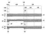
図1は、本開示の第1の実施の形態に係る多層配線基板の断面構成を表したものである。この多層配線基板は、プリント配線板またはインターポーザ基板として用いられるものであり、例えば、銅(Cu)箔よりなる第1配線層L1,後述する薄膜キャパシタCsを含む第2配線層L2,銅箔よりなる第3配線層L3,および銅箔よりなる第4配線層L4を、樹脂層11,12,13を間にして積層した4層プリント基板である。
(First embodiment)
FIG. 1 illustrates a cross-sectional configuration of the multilayer wiring board according to the first embodiment of the present disclosure. This multilayer wiring board is used as a printed wiring board or an interposer board. For example, a first wiring layer L1 made of copper (Cu) foil, a second wiring layer L2 containing a thin film capacitor Cs described later, and a copper foil. This is a four-layer printed circuit board in which a third wiring layer L3 and a fourth wiring layer L4 made of copper foil are laminated with
また、この多層配線基板には、プリント配線板またはインターポーザ基板として用いられる基板領域10Aと、ダイシングやルーター加工などの物理的な切削・切断を行うための加工領域10Bとが設けられている。基板領域10Aの一部には、薄膜キャパシタが内蔵された機能領域10Cが設けられており、この機能領域10C以外の領域は、キャパシタとして寄与しない周辺領域10Dとなっている。周辺領域10Dの一部には係留部10Eが設けられている。
In addition, the multilayer wiring board is provided with a
機能領域10Cは、多層配線基板に部品キャパシタを実装する代わりに、基板領域10Aに薄膜キャパシタを内蔵した領域である。プリント配線板やインターポーザ基板に薄膜キャパシタを内蔵することで、IC(Integrated Circuit;集積回路)の直下にデカップリングキャパシタを配置することが可能となる。
The functional region 10C is a region in which a thin film capacitor is built in the
このような機能領域10Cは、例えば、上述した第2配線層L2の銅箔に代えて、上部電極21および下部電極22の間に誘電層31を有する薄膜キャパシタCsを備えている。薄膜キャパシタCsの上部電極21および下部電極22には、貫通ビア21A,22Aがそれぞれ接続されている。
Such a functional region 10C includes, for example, a thin film capacitor Cs having a
上部電極21は、例えば、銅(Cu)などの金属箔により構成されている。また、上部電極21は、金属箔のほか、めっき,スパッタ,蒸着などによる導電層により構成されていてもよい。
The
誘電層31の構成材料は特に限定されないが、例えば、チタン酸ストロンチウム・バリウム(BST)(BaSrTiO),チタン酸バリウム(BTO)(BaTiO3),チタン酸ストロンチウム(STO)(SrTiO3)等が挙げられる。
The constituent material of the
下部電極22は、例えば、ニッケル(Ni)箔等の金属箔により構成されている。下部電極22の誘電層31に接する面は、ラッピング・ポリッシング等により平滑化されており、その表面ラフネスは例えばRz0.1μm以下であることが望ましい。誘電層31の厚さを薄くしても耐圧劣化やリーク電流を抑えることが可能となり、薄膜キャパシタCsの単位面積当たりの容量値を高めることが可能となるからである。
The
上部電極21の厚さは数μm〜数十μm、誘電層31の厚さは1μm前後、下部電極22の厚さは10μm〜100μmである。従って、薄膜キャパシタCsの厚さは、部品キャパシタに比べて一桁近く薄くすることが可能である。また、薄膜キャパシタCsは、両面銅張積層板と類似の上部電極(導電層)21/誘電層31/下部電極(導電層)22という層構成を有しているので、標準の基板プロセスと相性が良く、部品実装のためのランドを必要としないという利点もある。
The
係留部10Eは、上部電極21と同層の上部導電層41および下部電極22と同層の下部導電層42との間に誘電層31を有しており、その層構成は、機能領域10Cの薄膜キャパシタCsと同じである。しかしながら、下部導電層42の誘電層31に接する面のラフネスは、例えば少なくともRz4μm、好適にはRz8μmであり、下部電極22の誘電層31に接する面のラフネスよりも大きくなっている。換言すれば、下部導電層42の誘電層31に接する面は、下部電極22の誘電層31に接する面よりもラフネスが大きい粗面部43とされている。これにより、この多層配線基板では、薄膜キャパシタCsの上部電極21または下部電極22と誘電層31との界面での剥離を抑えることが可能となっている。
The
すなわち、薄膜キャパシタは部品キャパシタに比べると単位面積当たりの容量値が小さいという問題があった。薄膜キャパシタで実現可能な単位面積当たりの容量値は数μF/cm2である。単位面積当たりの容量値を向上させるためには、誘電層の比誘電率を大きくするか、誘電層の厚さを薄くする必要がある。 That is, the thin film capacitor has a problem that the capacitance value per unit area is smaller than that of the component capacitor. The capacitance value per unit area that can be realized by the thin film capacitor is several μF / cm 2 . In order to improve the capacitance value per unit area, it is necessary to increase the relative dielectric constant of the dielectric layer or reduce the thickness of the dielectric layer.
誘電層の比誘電率を大きくするためには、誘電層の材料を変えるのが効果的である。しかしながら、薄膜キャパシタでは、既に、部品キャパシタでも用いられている強誘電膜であるチタン酸ストロンチウムやチタン酸バリウム、チタン酸バリウムストロンチウム等を用いているため、大幅な比誘電率の向上は期待できない。 In order to increase the relative dielectric constant of the dielectric layer, it is effective to change the material of the dielectric layer. However, since the thin film capacitor uses a strontium titanate, a barium titanate, a barium strontium titanate, or the like, which is a ferroelectric film that is already used in a component capacitor, it cannot be expected that the relative dielectric constant is greatly improved.
一方、誘電層の厚さについては、理論的には誘電層の厚さに反比例して容量値は増えることになるため、誘電層を薄くすることは非常に有効である。ただし、実際には導電層に凹凸が存在するため、誘電層の膜厚を単純に薄くするだけでは局所的に誘電層の膜厚が薄くなる部分の影響が大きくなってしまい、そのため、大幅な耐圧劣化、及び大幅なリーク電流の増加を招くことになる。 On the other hand, regarding the thickness of the dielectric layer, the capacitance value increases theoretically in inverse proportion to the thickness of the dielectric layer, so it is very effective to reduce the thickness of the dielectric layer. However, since the conductive layer actually has irregularities, simply reducing the thickness of the dielectric layer increases the influence of the portion where the thickness of the dielectric layer is locally reduced. This will cause deterioration of the breakdown voltage and a significant increase in leakage current.
そこで、誘電層を形成する前に、導電層の表面を研磨等によりラフネスを改善させることで、局所的に誘電層の膜厚が薄くなる部分を無くすことが可能となり、誘電膜の膜厚を薄くすることが可能となる。 Therefore, by improving the roughness of the surface of the conductive layer by polishing or the like before forming the dielectric layer, it becomes possible to eliminate a portion where the thickness of the dielectric layer is locally thinned, and to reduce the thickness of the dielectric film. It can be made thinner.
しかし、その一方で、導電層の表面ラフネスが改善する悪影響として、導電層と誘電層の密着性が低減してしまうことがあげられる。導電層と誘電層の密着性の低減は、その界面での剥離現象を引き起こすリスクを高めることになる。界面の剥離現象は、キャパシタとしての設計電気容量とのズレを大きくしたり、設計品質を満たさないことに繋がる。また、プリント配線板やインターポーザ基板としてのデラミネーション発生の起点となり、はんだリフロー等の加熱衝撃を受けることで層間剥離が生じたり、製品使用途中の発生熱による剥離が誘発され、製品寿命を短命化させる原因となってしまうという問題があった。 On the other hand, an adverse effect of improving the surface roughness of the conductive layer is that the adhesion between the conductive layer and the dielectric layer is reduced. Reduction of the adhesion between the conductive layer and the dielectric layer increases the risk of causing a peeling phenomenon at the interface. The delamination phenomenon at the interface leads to an increase in deviation from the design capacitance as a capacitor or failure to satisfy the design quality. In addition, delamination occurs as a printed wiring board and interposer board, and delamination occurs due to heat shock such as solder reflow, and peeling due to heat generated during product use is induced, shortening the product life. There was a problem of causing it to occur.
そこで、本実施の形態では、係留部10Eにおける下部導電層42の誘電層31に接する面のラフネスを、機能領域10Cにおける薄膜キャパシタCsの下部電極22の誘電層31に接する面のラフネスよりも大きくするようにしている。これにより、係留部10Eに、下部導電層42と誘電層31との密着性を向上させるアンカー(係留)機能をもたせて、機能領域10Cにおいて薄膜キャパシタCsの上部電極21または下部電極22と誘電層31との界面での剥離を抑えることが可能となる。
Therefore, in the present embodiment, the roughness of the surface of the lower
係留部10Eは、図2に示したように、外形線10F、つまり基板領域10Aと加工領域10Bとの境界線に沿って設けられていることが好ましい。外形線10Fは、プリント配線板やインターポーザ基板のエッジ部分に相当し、ダイシングやルータ加工等の物理的な切削によるダメージにさらされる領域となる。この部分が、薄膜キャパシタCsの上部電極21または下部電極22と誘電層31との界面での剥離を引き起こすリスクが最も高い場所の一つである。従って、係留部10Eを外形線10Fに沿って設けることにより、薄膜キャパシタCsの上部電極21および下部電極22と誘電層31との界面での剥離を抑える効果を更に大きくすることが可能となる。
As shown in FIG. 2, the
上部導電層41および下部導電層42は、それぞれ、上部電極21および下部電極22と同様の材料により構成されている。上部導電層41および下部導電層42は、それぞれ、上部電極21および下部電極22と連続して(共通層として)設けられていてもよいし、上部電極21および下部電極22とは非連続に(別の層として)設けられていてもよい。
The upper
誘電層31は、機能領域10Cと周辺領域10Dとの共通層として(一つの連続した相として)設けられていることが好ましい。一般的な多層配線板の製造ラインにある装置での加工が難しいからである。
The
このような多層配線基板は、例えば、次のようにして製造することができる。 Such a multilayer wiring board can be manufactured as follows, for example.
図3は、この多層配線基板の製造方法の流れを表し、図4ないし図7は、図3に示した製造方法を工程順に表したものである。まず、図4(A)に示したように、下部電極22および下部導電層42の構成材料として、ニッケル箔等の金属箔51を用意する(ステップS101)。
FIG. 3 shows the flow of the manufacturing method of the multilayer wiring board, and FIGS. 4 to 7 show the manufacturing method shown in FIG. 3 in the order of steps. First, as shown in FIG. 4A, a
次いで、同じく図4(A)に示したように、この金属箔51の表面に対して、ラッピング・ポリッシング等により平滑化処理を行い、表面ラフネスを改善させる(ステップS102)。金属箔51の表面ラフネスは、例えばRz0.1μm以下になっているのが望ましい。これにより、機能領域10Cの下部電極22となる領域のラフネスが改善し、薄膜キャパシタCsの単位面積当たりの容量値を向上させることが可能となる。
Next, as shown in FIG. 4A, the surface of the
続いて、図4(B)に示したように、金属箔51の一部、具体的には、薄膜キャパシタCsとして寄与させない周辺領域10Dの一部のラフネスを悪化させる(ステップS103)。そのラフネスは例えば少なくともRz4μm、好適にはRz8μmとすることが望ましい。これにより、係留部10Eの下部導電層42となる領域のラフネスを、機能領域10Cの下部電極22となる領域のラフネスよりも大きく(荒く)させて、粗面部43を形成する。
Subsequently, as shown in FIG. 4B, the roughness of a part of the
金属箔51の一部のラフネスを悪化させる手法としては、例えば、レーザ照射(レーザ加工)を用いることが可能である。また、例えば、金属箔51をドライフィルムフォトレジストで覆い、パターニングにより一部に開口を設け、薬液を用いた粗化処理により、金属箔51の一部のラフネスを悪化させる方法でもよい。
As a method of deteriorating the roughness of a part of the
続いて、図4(C)に示したように、金属箔51の表面の全面に誘電層31を設ける(ステップS104)。誘電層41の形成方法としては、例えば、いわゆるゾル−ゲル法、誘電体フィラーとバインダー樹脂とを含む誘電体フィラー含有樹脂溶液を用いて塗工により誘電層を形成する塗工法、誘電体フィラーを含有したフィルムをラミネートする方法、スパッタ、蒸着等、種々の公知の方法を採用することが可能である。
Subsequently, as shown in FIG. 4C, the
そののち、図4(D)に示したように、誘電層31の上に、上部電極21および上部導電層41を形成するための導電材料層52を設ける(ステップS105)。導電材料層52の形成方法としては、金属箔を用いて張り合わせる方法、めっき法で導電材料層52を形成する方法、スパッタ、蒸着等、公知の種々の方法を採用することが可能である。
After that, as shown in FIG. 4D, a
誘電層31の上に導電材料層52を設けたのち、例えばエッチング、より具体的にはウェットエッチングにより、金属箔51を所定の形状に成形し、加工領域10Bの金属箔51を選択的に除去し、基板領域10Aのみに金属箔51を残存させる。これにより、図5(A)に示したように、機能領域10Cには薄膜キャパシタCsの下部電極22が形成され、ラフネスを悪化させた領域には、誘電層31および下部導電層42が積層された係留部10Eが形成される(ステップS106)。
After providing the
下部電極22および係留部10Eを形成したのち、図5(B)ないし図5(E)に示したように、下部電極22および下部導電層42の裏面に、第3配線層L3を形成するための金属箔53を、樹脂層12を間にして貼り合わせる。
After forming the
金属箔53の貼り合わせを行ったのち、図6(A)に示したように、例えばエッチングにより、導電材料層52を所定の形状に成形して、機能領域10Cに薄膜キャパシタCsの上部電極21を形成すると共に、係留部10Eに上部導電層41を形成する(ステップS107)。これにより、機能領域10Cには、上部電極21および下部電極22の間に誘電層31を有する薄膜キャパシタCsが形成される一方、周辺領域10Dの一部に、上部導電層41および下部導電層42の間に誘電層31を有する係留部10Eが形成される。
After the
これと同時に、同じく図6(A)に示したように、金属箔53を所定の形状に成形して第3配線層L3を形成する(ステップS108)。
At the same time, as shown in FIG. 6A, the
金属箔51,53を成形したのち、図6(B)ないし図6(D)に示したように、上部電極21および上部導電層41の上に、第1配線層L1を形成するための金属箔54を、樹脂層11を間にして貼り合わせる。また、図6(D)ないし図6(F)、および図7(A)に示したように、第3配線層L3の裏面に、第4配線層L4を形成するための金属箔55を、樹脂層13を間にして貼り合わせる。
After forming the metal foils 51 and 53, the metal for forming the first wiring layer L1 on the
金属箔54,55の貼り合わせを行ったのち、図7(B)に示したように、例えばエッチングにより、金属箔54,55を所定の形状に成形して第1配線層L1および第4配線層L4を形成する(ステップS109)。 After the metal foils 54 and 55 are bonded together, as shown in FIG. 7B, the metal foils 54 and 55 are formed into a predetermined shape by etching, for example, to form the first wiring layer L1 and the fourth wiring. Layer L4 is formed (step S109).
最後に、同じく図7(B)に示したように、薄膜キャパシタCsの上部電極21および下部電極22に、例えばレーザ加工により、貫通ビア21A,22Aをそれぞれ接続する。以上により、図1に示した多層配線基板が完成する。
Finally, as shown in FIG. 7B, the through
この多層配線基板では、係留部10Eにおける下部導電層42の誘電層31に接する面のラフネスが、機能領域10Cにおける下部電極22の誘電層31に接する面のラフネスよりも大きくなっている。よって、下部導電層42の誘電層31に接する面が荒れて表面積が増大することにより、下部導電層42と誘電層31との密着性が向上する。これにより、機能領域10Cにおいて薄膜キャパシタCsの上部電極21および下部電極22と誘電層31との界面での剥離が抑えられる。
In this multilayer wiring board, the roughness of the surface in contact with the
また、下部電極22の誘電層31に接する面は、ラッピング・ポリッシング等により平滑化され、そのラフネスは例えばRz0.1μm以下とされているので、誘電層31の厚さを薄くしても耐圧劣化やリーク電流が抑えられている。よって、薄膜キャパシタCsの単位面積当たりの容量値が向上する。
Further, the surface of the
これに対して、例えば図8に示したように、係留部10Eを設けず、薄膜キャパシタの容量を高めるために上部電極121および下部電極122のラフネスを改善した場合には、ラフネス改善の悪影響として、上部電極121または下部電極122と誘電層131との密着性が低減してしまっていた。上部電極121または下部電極122と誘電層131との密着性の低減は、その界面での剥離現象を引き起こすリスクを高めることになっていた。界面の剥離現象は、キャパシタとしての設計電気容量とのズレを大きくしたり、設計品質を満たさないことに繋がっていた。また、プリント配線板やインターポーザ基板としてのデラミネーション発生の起点となり、はんだリフロー等の加熱衝撃を受けることで層間剥離が生じたり、製品使用途中の発生熱による剥離が誘発され、製品寿命を短命化させる原因となってしまっていた。なお、図8においては、図1に対応する構成要素には100番台の同一の符号を付している。
On the other hand, for example, as shown in FIG. 8, when the roughness of the
このように本実施の形態では、係留部10Eにおける下部導電層42の誘電層31に接する面のラフネスを、機能領域10Cにおける薄膜キャパシタCsの下部電極22の誘電層31に接する面のラフネスよりも大きくするようにしている。よって、係留部10Eにおいて下部導電層42と誘電層31との密着性を向上させ、機能領域10Cにおいて薄膜キャパシタCsの上部電極21または下部電極22と誘電層31との界面での剥離を抑えることが可能となる。
Thus, in the present embodiment, the roughness of the surface of the lower
また、係留部10Eを、外形線10F、つまり基板領域10Aと加工領域10Bとの境界線に沿って設けるようにしたので、ダイシングやルータ加工等の物理的な切削によるダメージから基板領域10Aを保護し、薄膜キャパシタCsの上部電極21および下部電極22と誘電層31との界面での剥離を抑える効果を更に大きくすることが可能となる。
Further, since the
なお、上記実施の形態では、係留部10Eを外形線10Fに沿って配置する場合について説明したが、係留部10Eは必ずしも外形線10Fにある必要は無い。例えば、係留部10Eは、薄膜キャパシタCsとして寄与する機能領域10Cの周辺のみに設けられていてもよいし、薄膜キャパシタCsとして寄与する機能領域10C以外の周辺領域10Dの全てに設けられていてもよい。
In addition, although the case where the
また、上記実施の形態の製造方法では、最初に金属箔51の表面ラフネスを改善させる場合について説明した。しかしながら、本実施の形態の要点は、薄膜キャパシタCsとして寄与する機能領域10Cの下部電極22は、誘電層31を薄くすることによる高容量化を実現できるようにラフネスを改善しつつ、薄膜キャパシタCsとして寄与しない周辺領域10Dの少なくとも一部に、下部導電層42のラフネスを荒らした係留部10Eを設けることで必要とされる密着性を得ることにある。従って、イニシャルの金属箔51のラフネスが十分改善されている場合には、金属箔51の表面ラフネスの改善工程を行わず、金属箔51の表面の一部のラフネスを悪化させるだけでも、本実施の形態の効果は十分に得られる。
Moreover, in the manufacturing method of the said embodiment, the case where the surface roughness of the
更に、イニシャルの金属箔51のラフネスが、十分な密着性が得られるほど荒れている場合には、薄膜キャパシタCsとして寄与する機能領域10Cの下部電極22となる領域のみを選択的にラフネスを改善することによって、本実施の形態の効果は十分に得られることになる。下部電極22となる領域のラフネスを選択的に改善する方法としては、例えば、ドライフィルムパターニングにより、金属箔51のうち下部電極22となる領域のみ露出させておき、その部分を電界研磨等によりラフネス改善することによって可能となる。あるいは、選択的な電界研磨以外の他の方法を選択的な研磨を行うことも可能である。
Further, when the roughness of the
(第2の実施の形態)
図9は、本開示の第2の実施の形態に係る多層配線基板の断面構成を表したものである。この多層配線基板は、係留部10Eが、外形線10Fに加えて、周辺領域10Dの貫通孔10Gを囲んで設けられたものである。このことを除いては、この多層配線基板は第1の実施の形態と同様の構成、作用および効果を有している。よって、対応する構成要素には同一の符号を付して説明する。
(Second Embodiment)
FIG. 9 illustrates a cross-sectional configuration of a multilayer wiring board according to the second embodiment of the present disclosure. In this multilayer wiring board, the
貫通孔10Gは、多層配線基板の積層方向の全体を貫通して設けられたドリル貫通孔である。このような貫通孔10Gの周辺は、ドリル加工による物理的な切削にさらされる領域となり、この部分も、薄膜キャパシタの導電層と誘電層の界面での剥離現象を引き起こすリスクが最も高い場所の一つである。従って、係留部10Eを、貫通孔10Gを囲んで配置することにより、薄膜キャパシタCsの上部電極21および下部電極22と誘電層31との界面での剥離を抑える効果を更に大きくすることが可能となる。
The through hole 10 </ b> G is a drill through hole provided through the entire multilayer wiring board in the stacking direction. The periphery of such a through-
この多層配線基板は、例えば次のようにして製造することができる。 This multilayer wiring board can be manufactured, for example, as follows.
図10ないし図12は、この多層配線基板の製造方法を工程順に表したものである。なお、製造方法の流れは第1の実施の形態と同様であるので、以下の説明においても図3のステップを参照して説明する。また、第1の実施の形態と重複する工程については図4を参照して説明する。 10 to 12 show the manufacturing method of this multilayer wiring board in the order of steps. Since the flow of the manufacturing method is the same as that of the first embodiment, the following description will be given with reference to the steps in FIG. In addition, steps overlapping with those in the first embodiment will be described with reference to FIG.
まず、第1の実施の形態と同様にして、図4(A)に示した工程により、下部電極22および下部導電層42の構成材料として、ニッケル箔等の金属箔51を用意する(ステップS101)。
First, similarly to the first embodiment, a
次いで、第1の実施の形態と同様にして、同じく図4(A)に示した工程により、この金属箔51の表面に対して、ラッピング・ポリッシング等により平滑化処理を行い、表面ラフネスを改善させる(ステップS102)。
Next, in the same manner as in the first embodiment, the surface of the
続いて、第1の実施の形態と同様にして、図4(B)に示した工程により、図10(A)に示したように、金属箔51の一部、具体的には、薄膜キャパシタCsとして寄与させない周辺領域10Dの一部のラフネスを悪化させる(ステップS103)。これにより、係留部10Eの下部導電層42となる領域のラフネスを、機能領域10Cの下部電極22となる領域のラフネスよりも大きく(荒く)させて粗面部43を形成する。
Subsequently, in the same manner as in the first embodiment, a part of the
続いて、第1の実施の形態と同様にして、図4(C)に示した工程により、同じく図10(A)に示したように、金属箔51の表面の全面に誘電層31を設ける(ステップS104)。
Subsequently, as in the first embodiment, the
そののち、第1の実施の形態と同様にして、図4(D)に示した工程により、同じく図10(A)に示したように、誘電層31の上に、上部電極21および上部導電層41を形成するための導電材料層52を設ける(ステップS105)。
After that, as in the first embodiment, the
誘電層31の上に導電材料層52を設けたのち、例えばエッチングにより、金属箔51を所定の形状に成形し、加工領域10Bおよび貫通孔10Gの形成予定領域の金属箔51を選択的に除去する。これにより、図10(B)に示したように、機能領域10Cには薄膜キャパシタCsの下部電極22が形成され、ラフネスを悪化させた領域には、誘電層31および下部導電層42が積層された係留部10Eが形成される(ステップS106)。
After the
下部電極22および係留部10Eを形成したのち、図10(C)ないし図10(F)に示したように、下部電極22および下部導電層42の裏面に、第3配線層L3を形成するための金属箔53を、樹脂層12を間にして貼り合わせる。
After forming the
金属箔53の貼り合わせを行ったのち、図11(A)に示したように、例えばエッチングにより、導電材料層52を所定の形状に成形して、機能領域10Cに薄膜キャパシタCsの上部電極21を形成すると共に、係留部10Eに上部導電層41を形成する(ステップS107)。これにより、機能領域10Cには、上部電極21および下部電極22の間に誘電層31を有する薄膜キャパシタCsが形成される一方、周辺領域10Dの一部に、上部導電層41および下部導電層42の間に誘電層31を有する係留部10Eが形成される。
After the
これと同時に、同じく図11(A)に示したように、金属箔53を所定の形状に成形して第3配線層L3を形成する(ステップS108)。
At the same time, as shown in FIG. 11A, the
金属箔51,53を成形したのち、図11(B)ないし図11(D)に示したように、上部電極21および上部導電層41の上に、第1配線層L1を形成するための金属箔54を、樹脂層11を間にして貼り合わせる。また、図11(D)ないし図11(F)、および図12(A)に示したように、第3配線層L3の裏面に、第4配線層L4を形成するための金属箔55を、樹脂層13を間にして貼り合わせる。
After forming the metal foils 51 and 53, the metal for forming the first wiring layer L1 on the
金属箔54,55の貼り合わせを行ったのち、図12(B)に示したように、例えばエッチングにより、金属箔54,55を所定の形状に成形して第1配線層L1および第4配線層L4を形成する(ステップS109)。 After the metal foils 54 and 55 are bonded together, as shown in FIG. 12B, the metal foils 54 and 55 are formed into a predetermined shape by, for example, etching to form the first wiring layer L1 and the fourth wiring. Layer L4 is formed (step S109).
最後に、同じく図12(B)に示したように、薄膜キャパシタCsの上部電極21に、例えばレーザ加工により、貫通ビア21Aを接続する。また、ドリル加工により貫通孔10Gを設ける。以上により、図9に示した多層配線基板が完成する。
Finally, as shown in FIG. 12B, the through via 21A is connected to the
この多層配線基板では、係留部10Eが、外形線10Fに加えて、周辺領域10Dの貫通孔10Gを囲んで設けられている。よって、薄膜キャパシタCsの上部電極21および下部電極22と誘電層31との界面での剥離が更に確実に抑えられる。
In this multilayer wiring board, the
このように本実施の形態では、第1の実施の形態の効果に加えて、係留部10Eを、周辺領域10Dの貫通孔10Gを囲んで設けるようにしたので、薄膜キャパシタCsの上部電極21および下部電極22と誘電層31との界面での剥離を抑える効果を更に大きくすることが可能となる。
As described above, in the present embodiment, in addition to the effects of the first embodiment, the
なお、上記実施の形態では、係留部10Eを外形線10Fに沿って設けると共に、周辺領域10Dの貫通孔10Gを囲んで配置する場合について説明したが、係留部10Eは必ずしも外形線10Fおよび貫通孔10Gの周囲のみにある必要は無い。例えば、係留部10Eは、薄膜キャパシタCsとして寄与する機能領域10Cの周辺のみに設けられていてもよいし、薄膜キャパシタCsとして寄与する機能領域10C以外の周辺領域10Dの全てに設けられていてもよい。
In the above embodiment, the
(第3の実施の形態)
図13は、本開示の第3の実施の形態に係る多層配線基板の製造方法の流れを表し、図14は、図13に示した製造方法を工程順に表したものである。この製造方法は、金属箔51に誘電層31および導電材料層52を積層したのちにレーザ加工によるラフネス悪化工程を行うことにおいて第1の実施の形態とは異なるものである。なお、第1の実施の形態と重複する工程については図4ないし図7を参照して説明する。また、この製造方法は第1の実施の形態の多層配線基板を製造する場合に限られるものではないが、以下の説明では例えば第1の実施の形態のように係留部10Eを外形線10Fに沿って設ける場合を例として説明する。
(Third embodiment)
FIG. 13 shows the flow of the manufacturing method of the multilayer wiring board according to the third embodiment of the present disclosure, and FIG. 14 shows the manufacturing method shown in FIG. 13 in the order of steps. This manufacturing method is different from the first embodiment in that a roughness deterioration process by laser processing is performed after the
まず、第1の実施の形態と同様にして、図4(A)に示した工程により、図14(A)に示したように、下部電極22および下部導電層42の構成材料として、ニッケル箔等の金属箔51を用意する(ステップS101)。
First, in the same manner as in the first embodiment, nickel foil is used as a constituent material of the
次いで、第1の実施の形態と同様にして、同じく図4(A)に示した工程により、同じく図14(A)に示したように、この金属箔51の表面に対して、ラッピング・ポリッシング等により平滑化処理を行い、表面ラフネスを改善させる(ステップS102)。
Next, similarly to the first embodiment, the surface of the
続いて、図14(B)に示したように、金属箔51の表面の全面に誘電層31を設ける(ステップS203)。
Subsequently, as shown in FIG. 14B, the
そののち、図14(C)に示したように、誘電層31の上に、上部電極21および上部導電層41を形成するための導電材料層52を設ける(ステップS204)。
After that, as shown in FIG. 14C, a
誘電層31の上に導電材料層52を設けたのち、図14(D)に示したように、レーザ加工により、金属箔51の誘電層31に接する面の一部、具体的には、薄膜キャパシタCsとして寄与させない周辺領域10Dの一部のラフネスを悪化させる(ステップS205)。具体的には、例えば金属箔51の誘電層31に接する面のラフネスを悪化させるためには、金属箔51と誘電層31との界面に焦点を合わせてレーザ光LBを照射する。これにより、係留部10Eの下部導電層42となる領域のラフネスを、機能領域10Cの下部電極22となる領域のラフネスよりも大きく(荒く)させて粗面部43を形成する。
After providing the
レーザ加工を行ったのち、第1の実施の形態と同様にして、図5(A)に示した工程により、例えばエッチングにより、金属箔51を所定の形状に成形し、加工領域10Bの金属箔51を選択的に除去し、基板領域10Aのみに金属箔51を残存させる。これにより、機能領域10Cには薄膜キャパシタCsの下部電極22が形成され、ラフネスを悪化させた領域には、誘電層31および下部導電層42が積層された係留部10Eが形成される(ステップS206)。
After the laser processing, in the same manner as in the first embodiment, the
下部電極22および係留部10Eを形成したのち、第1の実施の形態と同様にして、図5(B)ないし図5(E)に示した工程により、下部電極22および下部導電層42の裏面に、第3配線層L3を形成するための金属箔53を、樹脂層12を間にして貼り合わせる。
After forming the
金属箔53の貼り合わせを行ったのち、第1の実施の形態と同様にして、図6(A)に示した工程により、例えばエッチングにより、導電材料層52を所定の形状に成形して、機能領域10Cに薄膜キャパシタCsの上部電極21を形成すると共に、係留部10Eに上部導電層41を形成する(ステップS207)。これにより、機能領域10Cには、上部電極21および下部電極22の間に誘電層31を有する薄膜キャパシタCsが形成される一方、周辺領域10Dの一部に、上部導電層41および下部導電層42の間に誘電層31を有する係留部10Eが形成される。
After the
これと同時に、第1の実施の形態と同様にして、同じく図6(A)に示した工程により、金属箔53を所定の形状に成形して第3配線層L3を形成する(ステップS108)。
At the same time, similarly to the first embodiment, the
金属箔51,53を成形したのち、第1の実施の形態と同様にして、図6(B)ないし図7(B)に示した工程により、金属箔54,55の貼り合わせを行い、この金属箔54,55を所定の形状に成形して第1配線層L1および第4配線層L4を形成する(ステップS109)。 After forming the metal foils 51 and 53, the metal foils 54 and 55 are bonded together by the steps shown in FIGS. 6B to 7B as in the first embodiment. The metal foils 54 and 55 are formed into a predetermined shape to form the first wiring layer L1 and the fourth wiring layer L4 (step S109).
最後に、第1の実施の形態と同様にして、同じく図7(B)に示した工程により、薄膜キャパシタCsの上部電極21および下部電極22に、例えばレーザ加工により、貫通ビア21A,22Aをそれぞれ接続する。以上により、図1に示した多層配線基板が完成する。
Finally, in the same manner as in the first embodiment, through
本実施の形態の多層配線基板の作用および効果は、第1の実施の形態と同様である。 The operation and effects of the multilayer wiring board of the present embodiment are the same as those of the first embodiment.
(変形例1)
なお、上記実施の形態では、係留部10Eの下部導電層42の誘電層31に接する面のラフネスを、上部電極21または下部電極22の誘電層31に接する面のラフネスよりも大きくする場合について説明した。しかしながら、図15に示したように、係留部10Eの上部導電層41の誘電層31に接する面のラフネスを、上部電極21または下部電極22の誘電層31に接する面のラフネスよりも大きくすることも可能である。換言すれば、上部導電層41の誘電層31に接する面を粗面部43とすることも可能である。その場合には、例えば導電材料層52と誘電層31との界面に焦点を合わせてレーザ光LBを照射する。
(Modification 1)
In the above embodiment, the case where the roughness of the surface of the lower
(変形例2)
あるいは、図16に示したように、係留部10Eの上部導電層41および下部導電層42の両方について、それらの誘電層31に接する面のラフネスを、上部電極21または下部電極22の誘電層31に接する面のラフネスよりも大きくすることも可能である。換言すれば、上部導電層41および下部導電層42の両方の誘電層31に接する面を粗面部43とすることも可能である。このようにすれば、係留部10Eの、上部導電層41および下部導電層42と誘電層31との密着性を向上させるアンカー機能を更に強めて、機能領域10Cにおいて薄膜キャパシタCsの上部電極21または下部電極22と誘電層31との界面での剥離をより確実に抑えることが可能となる。
(Modification 2)
Alternatively, as shown in FIG. 16, the roughness of the surface in contact with the
(第4の実施の形態)
図17は、本開示の第4の実施の形態に係る多層配線基板の製造方法の流れを表し、図18は、図17に示した製造方法を工程順に表したものである。この製造方法は、金属箔51を成形して下部導電層42を形成したのちにレーザ加工によるラフネス悪化工程を行うようにしたことにおいて第3の実施の形態とは異なるものである。なお、第1の実施の形態と重複する工程については図4ないし図7を参照し、第3の実施の形態と重複する工程については図14を参照して説明する。また、この製造方法は、第1の実施の形態の多層配線基板を製造する場合に限られるものではないが、本実施の形態では例えば第1の実施の形態のように係留部10Eを外形線10Fに沿って設ける場合を例として説明する。
(Fourth embodiment)
FIG. 17 shows the flow of the manufacturing method of the multilayer wiring board according to the fourth embodiment of the present disclosure, and FIG. 18 shows the manufacturing method shown in FIG. This manufacturing method is different from that of the third embodiment in that after the
まず、第1の実施の形態と同様にして、図4(A)に示した工程により、下部電極22および下部導電層42の構成材料として、ニッケル箔等の金属箔51を用意する(ステップS101)。
First, similarly to the first embodiment, a
次いで、第1の実施の形態と同様にして、同じく図4(A)に示した工程により、この金属箔51の表面に対して、ラッピング・ポリッシング等により平滑化処理を行い、表面ラフネスを改善させる(ステップS102)。
Next, in the same manner as in the first embodiment, the surface of the
続いて、第3の実施の形態と同様にして、図14(B)に示した工程により、金属箔51の表面の全面に誘電層31を設ける(ステップS203)。
Subsequently, in the same manner as in the third embodiment, the
そののち、第3の実施の形態と同様にして、図14(C)に示した工程により、図18(A)に示したように、誘電層31の上に、上部電極21および上部導電層41を形成するための導電材料層52を設ける(ステップS204)。
Thereafter, in the same manner as in the third embodiment, the
誘電層31の上に導電材料層52を設けたのち、第1の実施の形態と同様にして、図5(A)に示した工程により、図18(B)に示したように、例えばエッチングにより、金属箔51を所定の形状に成形し、加工領域10Bの金属箔51を選択的に除去し、基板領域10Aのみに金属箔51を残存させる。これにより、機能領域10Cには薄膜キャパシタCsの下部電極22が形成されると共に、周辺領域10Dの一部に、誘電層31および下部導電層42が積層された係留部10Eが形成される(ステップS305)。
After the
下部電極22および係留部10Eを形成したのち、図18(C)に示したように、レーザ加工により、下部導電層42の誘電層31に接する面の一部、具体的には、薄膜キャパシタCsとして寄与させない周辺領域10Dの一部のラフネスを悪化させる(ステップS306)。具体的には、例えば下部導電層42の誘電層31に接する面のラフネスを悪化させるためには、下部導電層42と誘電層31との界面に焦点を合わせてレーザ光LBを照射する。これにより、係留部10Eの下部導電層42の誘電層31に接する面のラフネスを、機能領域10Cの上部電極21または下部電極22の誘電層31に接する面のラフネスよりも大きく(荒く)させて粗面部43を形成する。
After forming the
レーザ加工を行ったのち、第1の実施の形態と同様にして、図5(B)ないし図5(E)に示した工程により、下部電極22および下部導電層42の裏面に、第3配線層L3を形成するための金属箔53を、樹脂層12を間にして貼り合わせる。
After the laser processing, the third wiring is formed on the back surface of the
金属箔53の貼り合わせを行ったのち、第1の実施の形態と同様にして、図6(A)に示した工程により、例えばエッチングにより、導電材料層52を所定の形状に成形して、機能領域10Cに薄膜キャパシタCsの上部電極21を形成すると共に、係留部10Eに上部導電層41を形成する(ステップS307)。これにより、機能領域10Cには、上部電極21および下部電極22の間に誘電層31を有する薄膜キャパシタCsが形成される一方、周辺領域10Dの一部に、上部導電層41および下部導電層42の間に誘電層31を有する係留部10Eが形成される。
After the
これと同時に、第1の実施の形態と同様にして、同じく図6(A)に示した工程により、金属箔53を所定の形状に成形して第3配線層L3を形成する(ステップS108)。
At the same time, similarly to the first embodiment, the
金属箔51,53を成形したのち、第1の実施の形態と同様にして、図6(B)ないし図7(B)に示した工程により、金属箔54,55の貼り合わせを行い、この金属箔54,55を所定の形状に成形して第1配線層L1および第4配線層L4を形成する(ステップS109)。 After forming the metal foils 51 and 53, the metal foils 54 and 55 are bonded together by the steps shown in FIGS. 6B to 7B as in the first embodiment. The metal foils 54 and 55 are formed into a predetermined shape to form the first wiring layer L1 and the fourth wiring layer L4 (step S109).
最後に、第1の実施の形態と同様にして、同じく図7(B)に示した工程により、薄膜キャパシタCsの上部電極21および下部電極22に、例えばレーザ加工により、貫通ビア21A,22Aをそれぞれ接続する。以上により、図1に示した多層配線基板が完成する。
Finally, in the same manner as in the first embodiment, through
この多層配線基板の作用および効果は、第1の実施の形態と同様である。 The operation and effect of this multilayer wiring board are the same as those in the first embodiment.
なお、上記第3の実施の形態の変形例1(図15)および変形例2(図16)は本実施の形態にも適用可能である。 Note that the first modification (FIG. 15) and the second modification (FIG. 16) of the third embodiment can also be applied to this embodiment.
(第5の実施の形態)
図19は、本開示の第4の実施の形態に係る多層配線基板の製造方法の流れを表し、図20および図21は、図19に示した製造方法を工程順に表したものである。この製造方法は、薄膜キャパシタCsを形成したのちにレーザ加工によるラフネス悪化工程を行うようにしたことにおいて第3の実施の形態とは異なるものである。なお、第1の実施の形態と重複する工程については図4ないし図7を参照し、第3の実施の形態と重複する工程については図14を参照して説明する。また、この製造方法は、第1の実施の形態の多層配線基板を製造する場合に限られるものではないが、本実施の形態では例えば第1の実施の形態のように係留部10Eを外形線10Fに沿って設ける場合を例として説明する。
(Fifth embodiment)
FIG. 19 shows the flow of the manufacturing method of the multilayer wiring board according to the fourth embodiment of the present disclosure, and FIGS. 20 and 21 show the manufacturing method shown in FIG. 19 in the order of steps. This manufacturing method is different from the third embodiment in that the roughness deterioration process by laser processing is performed after the thin film capacitor Cs is formed. In addition, about the process which overlaps with 1st Embodiment, refer to FIG. 4 thru | or FIG. 7, and about the process which overlaps with 3rd Embodiment, it demonstrates with reference to FIG. Further, this manufacturing method is not limited to the case of manufacturing the multilayer wiring board of the first embodiment, but in this embodiment, for example, the
まず、第1の実施の形態と同様にして、図4(A)に示した工程により、下部電極22および下部導電層42の構成材料として、ニッケル箔等の金属箔51を用意する(ステップS101)。
First, similarly to the first embodiment, a
次いで、第1の実施の形態と同様にして、同じく図4(A)に示した工程により、この金属箔51の表面に対して、ラッピング・ポリッシング等により平滑化処理を行い、表面ラフネスを改善させる(ステップS102)。
Next, in the same manner as in the first embodiment, the surface of the
続いて、第3の実施の形態と同様にして、図14(B)に示した工程により、金属箔51の表面の全面に誘電層31を設ける(ステップS203)。
Subsequently, in the same manner as in the third embodiment, the
そののち、第3の実施の形態と同様にして、図14(C)に示した工程により、図20(A)に示したように、誘電層31の上に、上部電極21および上部導電層41を形成するための導電材料層52を設ける(ステップS204)。
After that, in the same manner as in the third embodiment, the
誘電層31の上に導電材料層52を設けたのち、第1の実施の形態と同様にして、図5(A)に示した工程により、図20(B)に示したように、例えばエッチングにより、金属箔51を所定の形状に成形し、加工領域10Bの金属箔51を選択的に除去し、基板領域10Aのみに金属箔51を残存させる。これにより、機能領域10Cには薄膜キャパシタCsの下部電極22が形成されると共に、周辺領域10Dの一部に、誘電層31および下部導電層42が積層された係留部10Eが形成される(ステップS405)。
After the
下部電極22および係留部10Eを形成したのち、第1の実施の形態と同様にして、図5(B)ないし図5(E)に示した工程により、図20(C)ないし図20(F)に示したように、下部電極22および下部導電層42の裏面に、第3配線層L3を形成するための金属箔53を、樹脂層12を間にして貼り合わせる。
After forming the
金属箔53の貼り合わせを行ったのち、第1の実施の形態と同様にして、図6(A)に示した工程により、図21(A)に示したように、例えばエッチングにより、導電材料層52を所定の形状に成形して、機能領域10Cに薄膜キャパシタCsの上部電極21を形成すると共に、係留部10Eに上部導電層41を形成する(ステップS406)。これにより、機能領域10Cには、上部電極21および下部電極22の間に誘電層31を有する薄膜キャパシタCsが形成される一方、周辺領域10Dの一部に、上部導電層41および下部導電層42の間に誘電層31を有する係留部10Eが形成される。
After the
これと同時に、第1の実施の形態と同様にして、同じく図6(A)に示した工程により、同じく図21(A)に示したように、金属箔53を所定の形状に成形して第3配線層L3を形成する(ステップS407)。
At the same time, similarly to the first embodiment, the
上部電極21および上部導電層41を形成したのち、図21(B)に示したように、レーザ加工により、下部導電層42の誘電層31に接する面の一部、具体的には、薄膜キャパシタCsとして寄与させない周辺領域10Dの一部のラフネスを悪化させる(ステップS408)。具体的には、例えば下部導電層42の誘電層31に接する面のラフネスを悪化させるためには、下部導電層42と誘電層31との界面に焦点を合わせてレーザ光LBを照射する。これにより、係留部10Eの下部導電層42の誘電層31に接する面のラフネスを、機能領域10Cの上部電極21または下部電極22の誘電層31に接する面のラフネスよりも大きく(荒く)させて粗面部43を形成する。
After forming the
金属箔51,53を成形したのち、第1の実施の形態と同様にして、図6(B)ないし図7(B)に示した工程により、金属箔54,55の貼り合わせを行い、この金属箔54,55を所定の形状に成形して第1配線層L1および第4配線層L4を形成する(ステップS109)。 After forming the metal foils 51 and 53, the metal foils 54 and 55 are bonded together by the steps shown in FIGS. 6B to 7B as in the first embodiment. The metal foils 54 and 55 are formed into a predetermined shape to form the first wiring layer L1 and the fourth wiring layer L4 (step S109).
最後に、第1の実施の形態と同様にして、同じく図7(B)に示した工程により、薄膜キャパシタCsの上部電極21および下部電極22に、例えばレーザ加工により、貫通ビア21A,22Aをそれぞれ接続する。以上により、図1に示した多層配線基板が完成する。
Finally, in the same manner as in the first embodiment, through
この多層配線基板の作用および効果は、第1の実施の形態と同様である。 The operation and effect of this multilayer wiring board are the same as those in the first embodiment.
(変形例3)
なお、上記実施の形態では、金属箔51および導電材料層52を成形して薄膜キャパシタCsおよび係留部10Eを形成したのちにレーザ加工を行うようにした場合について説明した。しかしながら、例えば図22に示したように、第1配線層L1および第4配線層L4を形成し(ステップS109)、薄膜キャパシタCsが多層配線基板に内蔵されたのちにレーザ加工を行う(ステップS408)ことも可能である。
(Modification 3)
In the above embodiment, the case where the laser processing is performed after the
また、上記第3の実施の形態の変形例1(図15)および変形例2(図16)は、本実施の形態または変形例3にも適用可能である。 Further, the first modification (FIG. 15) and the second modification (FIG. 16) of the third embodiment are also applicable to the present embodiment or the third modification.
(第6の実施の形態)
図23は、本開示の第6の実施の形態に係る多層配線基板の断面構成を表したものである。この多層配線基板は、係留部10Eにおいて、上部導電層41と下部導電層42とが、連結部44を介して誘電層31を貫通して物理的につながっており、電気的にも短絡(ショート)しているものである。これにより、この多層配線基板では、第1の実施の形態と同様に、薄膜キャパシタCsの上部電極21または下部電極22と誘電層31との界面での剥離を抑えることが可能となっている。このことを除いては、本実施の形態は第1の実施の形態と同様の構成、作用および効果を有している。
(Sixth embodiment)
FIG. 23 illustrates a cross-sectional configuration of a multilayer wiring board according to the sixth embodiment of the present disclosure. In this multilayer wiring board, in the
この多層配線基板は、例えば、次のようにして製造することができる。 This multilayer wiring board can be manufactured, for example, as follows.
図24は、この多層配線基板の製造方法の流れを表したものである。なお、第1の実施の形態と重複する工程については図4ないし図7を参照し、第3の実施の形態と重複する工程については図14を参照して説明する。また、この製造方法は第1の実施の形態の多層配線基板を製造する場合に限られるものではないが、以下の説明では例えば第1の実施の形態のように係留部10Eを外形線10Fに沿って設ける場合を例として説明する。
FIG. 24 shows the flow of the manufacturing method of this multilayer wiring board. In addition, about the process which overlaps with 1st Embodiment, refer to FIG. 4 thru | or FIG. 7, and the process which overlaps with 3rd Embodiment is demonstrated with reference to FIG. In addition, this manufacturing method is not limited to the case of manufacturing the multilayer wiring board of the first embodiment, but in the following description, for example, the
まず、第1の実施の形態と同様にして、図4(A)に示した工程により、下部電極22および下部導電層42の構成材料として、ニッケル箔等の金属箔51を用意する(ステップS101)。
First, similarly to the first embodiment, a
次いで、第1の実施の形態と同様にして、同じく図4(A)に示した工程により、この金属箔51の表面に対して、ラッピング・ポリッシング等により平滑化処理を行い、表面ラフネスを改善させる(ステップS102)。
Next, in the same manner as in the first embodiment, the surface of the
続いて、第3の実施の形態と同様にして、図14(B)に示した工程により、金属箔51の表面の全面に誘電層31を設ける(ステップS203)。
Subsequently, in the same manner as in the third embodiment, the
そののち、第3の実施の形態と同様にして、図14(C)に示した工程により、誘電層31の上に、上部電極21および上部導電層41を形成するための導電材料層52を設ける(ステップS204)。
After that, similarly to the third embodiment, a
誘電層31の上に導電材料層52を設けたのち、レーザ加工により金属箔51と導電材料層52とを、連結部44を介して誘電層31を貫通して物理的につなげる(ステップS505)。
After the
レーザ加工を行ったのち、第1の実施の形態と同様にして、図5(A)に示した工程により、例えばエッチングにより、金属箔51を所定の形状に成形し、加工領域10Bの金属箔51を選択的に除去し、基板領域10Aのみに金属箔51を残存させる。これにより、機能領域10Cには薄膜キャパシタCsの下部電極22が形成され、金属箔51と導電材料層52とを物理的につなげた領域には、誘電層31および下部導電層42が積層された係留部10Eが形成される(ステップS506)。その際、係留部10Eは薄膜キャパシタCsとして寄与しない周辺領域10Dの一部なので、誘電層31がレーザ加工により焼損などのダメージを受け、下部導電層42(金属箔51)と導電材料層52とが連結部44を介して電気的に短絡(ショート)していても問題は生じない。
After the laser processing, in the same manner as in the first embodiment, the
下部電極22および係留部10Eを形成したのち、第1の実施の形態と同様にして、図5(B)ないし図5(E)に示した工程により、下部電極22および下部導電層42の裏面に、第3配線層L3を形成するための金属箔53を、樹脂層12を間にして貼り合わせる。
After forming the
金属箔53の貼り合わせを行ったのち、第1の実施の形態と同様にして、図6(A)に示した工程により、例えばエッチングにより、導電材料層52を所定の形状に成形して、機能領域10Cに薄膜キャパシタCsの上部電極21を形成すると共に、係留部10Eに上部導電層41を形成する(ステップS507)。これにより、機能領域10Cには、上部電極21および下部電極22の間に誘電層31を有する薄膜キャパシタCsが形成される一方、周辺領域10Dの一部に、上部導電層41および下部導電層42の間に誘電層31を有する係留部10Eが形成される。
After the
これと同時に、第1の実施の形態と同様にして、同じく図6(A)に示した工程により、金属箔53を所定の形状に成形して第3配線層L3を形成する(ステップS108)。
At the same time, similarly to the first embodiment, the
金属箔51,53を成形したのち、第1の実施の形態と同様にして、図6(B)ないし図7(B)に示した工程により、金属箔54,55の貼り合わせを行い、この金属箔54,55を所定の形状に成形して第1配線層L1および第4配線層L4を形成する(ステップS109)。 After forming the metal foils 51 and 53, the metal foils 54 and 55 are bonded together by the steps shown in FIGS. 6B to 7B as in the first embodiment. The metal foils 54 and 55 are formed into a predetermined shape to form the first wiring layer L1 and the fourth wiring layer L4 (step S109).
最後に、第1の実施の形態と同様にして、同じく図7(B)に示した工程により、薄膜キャパシタCsの上部電極21および下部電極22に、例えばレーザ加工により、貫通ビア21A,22Aをそれぞれ接続する。以上により、図23に示した多層配線基板が完成する。
Finally, in the same manner as in the first embodiment, through
また、この多層配線基板は、例えば、次のようにして製造することも可能である。 Moreover, this multilayer wiring board can also be manufactured as follows, for example.
図25は、この多層配線基板の他の製造方法の流れを表したものである。なお、第1の実施の形態と重複する工程については図4ないし図7を参照し、第3の実施の形態と重複する工程については図14を参照して説明する。また、この製造方法は、第1の実施の形態の多層配線基板を製造する場合に限られるものではないが、本実施の形態では例えば第1の実施の形態のように係留部10Eを外形線10Fに沿って設ける場合を例として説明する。
FIG. 25 shows the flow of another manufacturing method of this multilayer wiring board. In addition, about the process which overlaps with 1st Embodiment, refer to FIG. 4 thru | or FIG. 7, and the process which overlaps with 3rd Embodiment is demonstrated with reference to FIG. Further, this manufacturing method is not limited to the case of manufacturing the multilayer wiring board of the first embodiment, but in this embodiment, for example, the
まず、第1の実施の形態と同様にして、図4(A)に示した工程により、下部電極22および下部導電層42の構成材料として、ニッケル箔等の金属箔51を用意する(ステップS101)。
First, similarly to the first embodiment, a
次いで、第1の実施の形態と同様にして、同じく図4(A)に示した工程により、この金属箔51の表面に対して、ラッピング・ポリッシング等により平滑化処理を行い、表面ラフネスを改善させる(ステップS102)。
Next, in the same manner as in the first embodiment, the surface of the
続いて、第3の実施の形態と同様にして、図14(B)に示した工程により、金属箔51の表面の全面に誘電層31を設ける(ステップS203)。
Subsequently, in the same manner as in the third embodiment, the
そののち、第3の実施の形態と同様にして、図14(C)に示した工程により、誘電層31の上に、上部電極21および上部導電層41を形成するための導電材料層52を設ける(ステップS204)。
After that, similarly to the third embodiment, a
誘電層31の上に導電材料層52を設けたのち、第1の実施の形態と同様にして、図5(A)に示した工程により、例えばエッチングにより、金属箔51を所定の形状に成形し、加工領域10Bの金属箔51を選択的に除去し、基板領域10Aのみに金属箔51を残存させる。これにより、機能領域10Cには薄膜キャパシタCsの下部電極22が形成されると共に、周辺領域10Dの一部に、誘電層31および下部導電層42が積層された係留部10Eが形成される(ステップS605)。
After the
下部電極22および係留部10Eを形成したのち、レーザ加工により、係留部10Eにおける下部導電層42と導電材料層52とを、連結部44を介して誘電層31を貫通して物理的につなげる(ステップS606)。
After forming the
レーザ加工を行ったのち、第1の実施の形態と同様にして、図5(B)ないし図5(E)に示した工程により、下部電極22および下部導電層42の裏面に、第3配線層L3を形成するための金属箔53を、樹脂層12を間にして貼り合わせる。なお、金属箔53の貼り合わせは、レーザ加工の前に行うことも可能である。
After the laser processing, the third wiring is formed on the back surface of the
金属箔53の貼り合わせを行ったのち、第1の実施の形態と同様にして、図6(A)に示した工程により、例えばエッチングにより、導電材料層52を所定の形状に成形して、機能領域10Cに薄膜キャパシタCsの上部電極21を形成すると共に、係留部10Eに上部導電層41を形成する(ステップS607)。これにより、機能領域10Cには、上部電極21および下部電極22の間に誘電層31を有する薄膜キャパシタCsが形成される一方、周辺領域10Dの一部に、上部導電層41および下部導電層42の間に誘電層31を有する係留部10Eが形成される。
After the
また、第1の実施の形態と同様にして、同じく図6(A)に示した工程により、金属箔53を所定の形状に成形して第3配線層L3を形成する(ステップS108)。
Similarly to the first embodiment, the third wiring layer L3 is formed by forming the
金属箔51,53を成形したのち、第1の実施の形態と同様にして、図6(B)ないし図7(B)に示した工程により、金属箔54,55の貼り合わせを行い、この金属箔54,55を所定の形状に成形して第1配線層L1および第4配線層L4を形成する(ステップS109)。 After forming the metal foils 51 and 53, the metal foils 54 and 55 are bonded together by the steps shown in FIGS. 6B to 7B as in the first embodiment. The metal foils 54 and 55 are formed into a predetermined shape to form the first wiring layer L1 and the fourth wiring layer L4 (step S109).
最後に、第1の実施の形態と同様にして、同じく図7(B)に示した工程により、薄膜キャパシタCsの上部電極21および下部電極22に、例えばレーザ加工により、貫通ビア21A,22Aをそれぞれ接続する。以上により、図23に示した多層配線基板が完成する。
Finally, in the same manner as in the first embodiment, through
あるいは、この多層配線基板は、例えば、次のようにして製造することも可能である。 Alternatively, this multilayer wiring board can be manufactured, for example, as follows.
図26は、この多層配線基板の更に他の製造方法の流れを表したものである。なお、第1の実施の形態と重複する工程については図4ないし図7を参照し、第3の実施の形態と重複する工程については図14を参照して説明する。また、この製造方法は、第1の実施の形態の多層配線基板を製造する場合に限られるものではないが、本実施の形態では例えば第1の実施の形態のように係留部10Eを外形線10Fに沿って設ける場合を例として説明する。
FIG. 26 shows the flow of still another manufacturing method of this multilayer wiring board. In addition, about the process which overlaps with 1st Embodiment, refer to FIG. 4 thru | or FIG. 7, and the process which overlaps with 3rd Embodiment is demonstrated with reference to FIG. Further, this manufacturing method is not limited to the case of manufacturing the multilayer wiring board of the first embodiment, but in this embodiment, for example, the
まず、第1の実施の形態と同様にして、図4(A)に示した工程により、下部電極22および下部導電層42の構成材料として、ニッケル箔等の金属箔51を用意する(ステップS101)。
First, similarly to the first embodiment, a
次いで、第1の実施の形態と同様にして、同じく図4(A)に示した工程により、この金属箔51の表面に対して、ラッピング・ポリッシング等により平滑化処理を行い、表面ラフネスを改善させる(ステップS102)。
Next, in the same manner as in the first embodiment, the surface of the
続いて、第3の実施の形態と同様にして、図14(B)に示した工程により、金属箔51の表面の全面に誘電層31を設ける(ステップS203)。
Subsequently, in the same manner as in the third embodiment, the
そののち、第3の実施の形態と同様にして、図14(C)に示した工程により、誘電層31の上に、上部電極21および上部導電層41を形成するための導電材料層52を設ける(ステップS204)。
After that, similarly to the third embodiment, a
誘電層31の上に導電材料層52を設けたのち、第1の実施の形態と同様にして、図5(A)に示した工程により、例えばエッチングにより、金属箔51を所定の形状に成形し、加工領域10Bの金属箔51を選択的に除去し、基板領域10Aのみに金属箔51を残存させる。これにより、機能領域10Cには薄膜キャパシタCsの下部電極22が形成されると共に、周辺領域10Dの一部に、誘電層31および下部導電層42が積層された係留部10Eが形成される(ステップS705)。
After the
下部電極22および係留部10Eを形成したのち、第1の実施の形態と同様にして、図5(B)ないし図5(E)に示した工程により、下部電極22および下部導電層42の裏面に、第3配線層L3を形成するための金属箔53を、樹脂層12を間にして貼り合わせる。
After forming the
金属箔53の貼り合わせを行ったのち、第1の実施の形態と同様にして、図6(A)に示した工程により、例えばエッチングにより、導電材料層52を所定の形状に成形して、機能領域10Cに薄膜キャパシタCsの上部電極21を形成すると共に、係留部10Eに上部導電層41を形成する(ステップS706)。これにより、機能領域10Cには、上部電極21および下部電極22の間に誘電層31を有する薄膜キャパシタCsが形成される一方、周辺領域10Dの一部に、上部導電層41および下部導電層42の間に誘電層31を有する係留部10Eが形成される。
After the
これと同時に、第1の実施の形態と同様にして、同じく図6(A)に示した工程により、金属箔53を所定の形状に成形して第3配線層L3を形成する(ステップS707)。
At the same time, similarly to the first embodiment, the
上部電極21,上部導電層41および第3配線層L3を形成したのち、レーザ加工により、上部導電層41と下部導電層42とを、連結部44を介して誘電層31を貫通して物理的につなげる(ステップS708)。
After forming the
金属箔51,53を成形したのち、第1の実施の形態と同様にして、図6(B)ないし図7(B)に示した工程により、金属箔54,55の貼り合わせを行い、この金属箔54,55を所定の形状に成形して第1配線層L1および第4配線層L4を形成する(ステップS109)。 After forming the metal foils 51 and 53, the metal foils 54 and 55 are bonded together by the steps shown in FIGS. 6B to 7B as in the first embodiment. The metal foils 54 and 55 are formed into a predetermined shape to form the first wiring layer L1 and the fourth wiring layer L4 (step S109).
最後に、第1の実施の形態と同様にして、同じく図7(B)に示した工程により、薄膜キャパシタCsの上部電極21および下部電極22に、例えばレーザ加工により、貫通ビア21A,22Aをそれぞれ接続する。以上により、図23に示した多層配線基板が完成する。
Finally, in the same manner as in the first embodiment, through
なお、図26に示した製造方法において、変形例3と同様にして、図27に示したように、第1配線層L1および第4配線層L4を形成し(ステップS109)、薄膜キャパシタCsが多層配線基板に内蔵されたのちにレーザ加工を行う(ステップS708)ことも可能である。 In the manufacturing method shown in FIG. 26, the first wiring layer L1 and the fourth wiring layer L4 are formed as shown in FIG. 27 in the same manner as in the third modification (step S109), and the thin film capacitor Cs is formed. It is also possible to perform laser processing after being incorporated in the multilayer wiring board (step S708).
この多層配線基板では、係留部10Eにおける上部導電層41と下部導電層42とが、連結部44を介して誘電層31を貫通して物理的につながっているので、上部導電層41および下部導電層42の密着性が向上する。これにより、機能領域10Cにおいて薄膜キャパシタCsの上部電極21および下部電極22と誘電層31との界面での剥離が抑えられる。
In this multilayer wiring board, the upper
このように本実施の形態では、係留部10Eにおける上部導電層41と下部導電層42とを、誘電層31を貫通して物理的につなげるようにしている。よって、係留部10Eにおいて上部導電層41および下部導電層42の密着性を向上させ、機能領域10Cにおいて薄膜キャパシタCsの上部電極21または下部電極22と誘電層31との界面での剥離を抑えることが可能となる。
Thus, in the present embodiment, the upper
(変形例4)
なお、上記実施の形態では、係留部10Eにおいて、上部導電層41と下部導電層42とが、誘電層31を貫通して物理的につながっている場合について説明したが、本実施の形態と第1の実施の形態とを組み合わせることも可能である。例えば図28に示したように、係留部10Eにおいて、上部導電層41または下部導電層42の誘電層31に接する面のラフネスが、上部電極21または下部電極22の誘電層31に接する面のラフネスよりも大きく(換言すれば、上部導電層41または下部導電層42の誘電層31に接する面が粗面部43とされており)、かつ、上部導電層41と下部導電層42とが、誘電層31を貫通して物理的につながっていてもよい。係留部10Eは薄膜キャパシタCsとして寄与しない周辺領域10Dの一部であることから、ラフネス悪化工程において誘電層31がダメージを受けて(例えばレーザ加工により焼損してしまって)、上部導電層41と下部導電層42とが物理的につながり、電気的に短絡(ショート)してしまっても問題は生じない。
(Modification 4)
In the above embodiment, the case where the upper
(第7の実施の形態)
図29は、本開示の第7の実施の形態に係る多層配線基板の断面構成を表したものである。この多層配線基板7は、例えばインターポーザ基板として用いられるものであり、第1の実施の形態の薄膜キャパシタCsが内蔵された基板本体部71を有している。基板本体部71には、例えば外形線10Fに沿って、第1または第6の実施の形態と同様の係留部10Eが設けられている。
(Seventh embodiment)
FIG. 29 illustrates a cross-sectional configuration of a multilayer wiring board according to the seventh embodiment of the present disclosure. The
基板本体部71の上面には、薄膜キャパシタCsの上方に、半導体素子72が実装されている。半導体素子72が実装された基板本体部71の上面は、保護膜73で被覆されている。
A
また、図30に示したように、半導体素子72に代えて、ICチップ74などを実装することも可能である。
In addition, as shown in FIG. 30, an
この多層配線基板7は、例えば、第1,第3ないし第5の実施の形態と同様にして製造することができ、その作用および効果も第1または第6の実施の形態と同様である。
The
(第8の実施の形態)
図31は、本開示の第8の実施の形態に係る多層配線基板の断面構成を表したものである。この多層配線基板8は、例えば、PoPと呼ばれる多段に重ねられた構造のインターポーザ基板であり、第7の実施の形態に係る多層配線基板7を複数層(例えば図31では二層)重ねた構成を有している。
(Eighth embodiment)
FIG. 31 illustrates a cross-sectional configuration of a multilayer wiring board according to the eighth embodiment of the present disclosure. The
本実施の形態では、半導体素子72と、多層配線基板7の基板本体部71に埋め込まれた薄膜キャパシタCsとの間の配線距離を最短にすることが可能となり、半導体素子72から見たパッケージ全体のインダクタンスを低減することが可能となる。
In the present embodiment, it is possible to minimize the wiring distance between the
(第9の実施の形態)
図32は、本開示の第9の実施の形態に係る半導体装置の構成を表したものである。この半導体装置9は、例えばマザーボード80上に、DC/DC電源回路91と、バルクチップ92と、インターポーザ基板として第8の実施の形態に係る多層配線基板8とを実装したものである。マザーボード80は、第1配線層(GND)L1および第2配線層(電源供給配線)L2を、樹脂層81,82,83を間にして積層した構成を有するプリント配線基板である。マザーボード80内部には、第1配線層L1および第2配線層L2と、それらの間の樹脂層82とにより、上記第1または第6の実施の形態に係る薄膜キャパシタCsおよび係留部10Eが構成されている。
(Ninth embodiment)
FIG. 32 illustrates a configuration of a semiconductor device according to the ninth embodiment of the present disclosure. In the semiconductor device 9, for example, a DC / DC
この半導体装置では、マザーボード80が上記実施の形態の多層配線基板により構成されているので、機能領域10Cにおいて薄膜キャパシタCsの上部電極21または下部電極22と誘電層31との界面での剥離が抑えられており、製品寿命が長くなる。
In this semiconductor device, since the
以上、実施の形態を挙げて本開示を説明したが、本開示は上記実施の形態に限定されるものではなく、種々の変形が可能である。例えば、上記実施の形態では、周辺領域10Dの一部に係留部10Eを設ける場合について説明したが、係留部10Eは、周辺領域10Dの少なくとも一部に設けられていればよい。例えば、係留部10Eは、周辺領域10Dの全部に設けられていてもよい。
While the present disclosure has been described with reference to the embodiment, the present disclosure is not limited to the above embodiment, and various modifications can be made. For example, although the case where the
また、上記実施の形態では、係留部10Eが上部導電層41および下部導電層42の間に誘電層31を積層した構成を有している場合について説明したが、係留部10Eは、誘電層31と下部導電層42とを積層した構成を有し、下部導電層42の誘電層31に接する面が粗面部43とされていてもよい。または、係留部10Eは、誘電層31と上部導電層41とを積層した構成を有し、上部導電層41の誘電層31に接する面が粗面部43とされていてもよい。
In the above-described embodiment, the
更に、例えば、上記実施の形態では、多層配線基板または半導体装置の構成を具体的に挙げて説明したが、全ての構成要素を備える必要はなく、また、他の構成要素を更に備えていてもよい。 Furthermore, for example, in the above-described embodiment, the configuration of the multilayer wiring board or the semiconductor device has been specifically described. However, it is not necessary to include all the components, and other components may be further included. Good.
なお、本技術は以下のような構成を取ることも可能である。
(1)
上部電極および下部電極の間に誘電層を有する薄膜キャパシタを備えた機能領域と、前記機能領域以外の周辺領域とを有し、
前記周辺領域の少なくとも一部に、前記誘電層および導電層が積層された係留部が設けられ、
前記導電層の前記誘電層に接する面のラフネスが、前記上部電極または前記下部電極の前記誘電層に接する面のラフネスよりも大きい
多層配線基板。
(2)
前記誘電層は、前記機能領域と前記周辺領域との共通層として設けられている
前記(1)記載の多層配線基板。
(3)
前記係留部が、外形線に沿って設けられている
前記(1)または(2)記載の多層配線基板。
(4)
前記周辺領域に貫通孔が設けられており、
前記係留部は、前記貫通孔を囲んで設けられている
前記(1)ないし(3)のいずれか1項に記載の多層配線基板。
(5)
前記係留部は、上部導電層および下部導電層の間に前記誘電層を有し、前記上部導電層と前記下部導電層とが、前記誘電層を貫通して物理的につながっている
前記(1)ないし(4)のいずれか1項に記載の多層配線基板。
(6)
金属箔の表面の一部のラフネスを悪化させる工程と、
前記金属箔の表面に誘電層および導電材料層をこの順に積層する工程と、
前記金属箔を成形することにより、薄膜キャパシタの下部電極を形成すると共に、前記ラフネスを悪化させた領域に、前記誘電層および下部導電層が積層された係留部を形成する工程と、
前記導電材料層を成形することにより、前記薄膜キャパシタの上部電極を形成する工程と
を含む多層配線基板の製造方法。
(7)
前記金属箔の表面の一部のラフネスを悪化させる工程の前に、前記金属箔の表面のうち少なくとも前記下部電極となる領域のラフネスを改善させる工程を含む
前記(6)記載の多層配線基板の製造方法。
(8)
前記ラフネスを悪化させる手法として、レーザ加工を用いる
前記(6)または(7)記載の多層配線基板の製造方法。
(9)
前記ラフネスを悪化させる手法として、薬液による粗化処理を用いる
前記(6)または(7)記載の多層配線基板の製造方法。
(10)
金属箔の表面に誘電層および導電材料層をこの順に積層する工程と、
レーザ加工により前記金属箔または前記導電材料層の前記誘電層に接する面の一部のラフネスを悪化させる工程と、
前記金属箔を成形することにより、薄膜キャパシタの下部電極を形成すると共に、前記ラフネスを悪化させた領域に、前記誘電層および下部導電層が積層された係留部を形成する工程と、
前記導電材料層を成形することにより、前記薄膜キャパシタの上部電極を形成すると共に、前記係留部に上部導電層を形成する工程と
を含む多層配線基板の製造方法。
(11)
金属箔の表面に誘電層および導電材料層をこの順に積層する工程と、
前記金属箔を成形することにより、薄膜キャパシタの下部電極を形成すると共に、前記誘電層および下部導電層が積層された係留部を形成する工程と、
レーザ加工により前記係留部における前記下部導電層または前記導電材料層の前記誘電層に接する面のラフネスを悪化させる工程と、
前記導電材料層を成形することにより、前記薄膜キャパシタの上部電極を形成する工程と
を含む多層配線基板の製造方法。
(12)
金属箔の表面に誘電層および導電材料層をこの順に積層する工程と、
前記金属箔を成形することにより、薄膜キャパシタの下部電極を形成すると共に、前記誘電層および下部導電層が積層された係留部を形成する工程と、
前記導電材料層を成形することにより、前記薄膜キャパシタの上部電極を形成すると共に、前記係留部に上部導電層を形成する工程と、
レーザ加工により前記係留部における前記上部導電層または前記下部導電層の前記誘電層に接する面のラフネスを悪化させる工程と
を含む多層配線基板の製造方法。
(13)
上部電極および下部電極の間に誘電層を有する薄膜キャパシタを備えた機能領域と、前記機能領域以外の周辺領域とを有し、
前記周辺領域の少なくとも一部に、上部導電層および下部導電層の間に前記誘電層を有する係留部が設けられ、
前記上部導電層と前記下部導電層とが、前記誘電層を貫通して物理的につながっている
多層配線基板。
(14)
金属箔の表面に誘電層および導電材料層をこの順に積層する工程と、
レーザ加工により前記金属箔と前記導電材料層とを、前記誘電層を貫通して物理的につなげる工程と、
前記金属箔を成形することにより、薄膜キャパシタの下部電極を形成すると共に、前記金属箔と前記導電材料層とを物理的につなげた領域に、前記誘電層および下部導電層が積層された係留部を形成する工程と、
前記導電材料層を成形することにより、前記薄膜キャパシタの上部電極を形成すると共に、前記係留部に上部導電層を形成する工程と
を含む多層配線基板の製造方法。
(15)
金属箔の表面に誘電層および導電材料層をこの順に積層する工程と、
前記金属箔を成形することにより、薄膜キャパシタの下部電極を形成すると共に、前記誘電層および下部導電層が積層された係留部を形成する工程と、
レーザ加工により前記係留部における前記下部導電層と前記導電材料層とを、前記誘電層を貫通して物理的につなげる工程と、
前記導電材料層を成形することにより、前記薄膜キャパシタの上部電極を形成すると共に、前記係留部に上部導電層を形成する工程と
を含む多層配線基板の製造方法。
(16)
金属箔の表面に誘電層および導電材料層をこの順に積層する工程と、
前記金属箔を成形することにより、薄膜キャパシタの下部電極を形成すると共に、前記誘電層および下部導電層が積層された係留部を形成する工程と、
前記導電材料層を成形することにより、前記薄膜キャパシタの上部電極を形成すると共に、前記係留部に上部導電層を形成する工程と、
レーザ加工により前記係留部における前記上部導電層と前記下部導電層とを、前記誘電層を貫通して物理的につなげる工程と
を含む多層配線基板の製造方法。
(17)
チップおよび多層配線基板を備え、
前記多層配線基板は、
上部電極および下部電極の間に誘電層を有する薄膜キャパシタを備えた機能領域と、前記機能領域以外の周辺領域とを有し、
前記周辺領域の少なくとも一部に、前記誘電層および導電層が積層された係留部が設けられ、
前記導電層の前記誘電層に接する面のラフネスが、前記上部電極または前記下部電極の前記誘電層に接する面のラフネスよりも大きい
半導体装置。
(18)
チップおよび多層配線基板を備え、
前記多層配線基板は、
上部電極および下部電極の間に誘電層を有する薄膜キャパシタを備えた機能領域と、前記機能領域以外の周辺領域とを有し、
前記周辺領域の少なくとも一部に、上部導電層および下部導電層の間に前記誘電層を有する係留部が設けられ、
前記上部導電層と前記下部導電層とが、前記誘電層を貫通して物理的につながっている
半導体装置。
In addition, this technique can also take the following structures.
(1)
A functional region including a thin film capacitor having a dielectric layer between the upper electrode and the lower electrode, and a peripheral region other than the functional region;
A mooring part in which the dielectric layer and the conductive layer are laminated is provided in at least a part of the peripheral region,
A multilayer wiring board, wherein a roughness of a surface of the conductive layer in contact with the dielectric layer is larger than a roughness of a surface of the upper electrode or the lower electrode in contact with the dielectric layer.
(2)
The multilayer wiring board according to (1), wherein the dielectric layer is provided as a common layer of the functional region and the peripheral region.
(3)
The multilayer wiring board according to (1) or (2), wherein the mooring portion is provided along an outline.
(4)
A through hole is provided in the peripheral region;
The multilayer wiring board according to any one of (1) to (3), wherein the mooring portion is provided so as to surround the through hole.
(5)
The mooring part has the dielectric layer between an upper conductive layer and a lower conductive layer, and the upper conductive layer and the lower conductive layer are physically connected through the dielectric layer. The multilayer wiring board according to any one of (4) to (4).
(6)
A process of deteriorating the roughness of a part of the surface of the metal foil;
Laminating a dielectric layer and a conductive material layer in this order on the surface of the metal foil;
Forming a lower electrode of a thin film capacitor by forming the metal foil, and forming a mooring portion in which the dielectric layer and the lower conductive layer are laminated in a region where the roughness is deteriorated;
Forming the upper electrode of the thin film capacitor by forming the conductive material layer.
(7)
Before the step of deteriorating the roughness of a part of the surface of the metal foil, the method includes a step of improving the roughness of at least the region serving as the lower electrode in the surface of the metal foil. Production method.
(8)
Laser processing is used as a technique for deteriorating the roughness. The method for manufacturing a multilayer wiring board according to (6) or (7).
(9)
The method for manufacturing a multilayer wiring board according to (6) or (7), wherein a roughening process using a chemical solution is used as a method of deteriorating the roughness.
(10)
Laminating a dielectric layer and a conductive material layer in this order on the surface of the metal foil;
Deteriorating the roughness of a part of the surface of the metal foil or the conductive material layer in contact with the dielectric layer by laser processing;
Forming a lower electrode of a thin film capacitor by forming the metal foil, and forming a mooring portion in which the dielectric layer and the lower conductive layer are laminated in a region where the roughness is deteriorated;
Forming the upper electrode of the thin film capacitor by forming the conductive material layer, and forming an upper conductive layer on the mooring portion.
(11)
Laminating a dielectric layer and a conductive material layer in this order on the surface of the metal foil;
Forming the lower electrode of the thin film capacitor by forming the metal foil, and forming an anchoring portion in which the dielectric layer and the lower conductive layer are laminated;
Worsening the roughness of the surface of the mooring portion in contact with the dielectric layer of the lower conductive layer or the conductive material layer by laser processing;
Forming the upper electrode of the thin film capacitor by forming the conductive material layer.
(12)
Laminating a dielectric layer and a conductive material layer in this order on the surface of the metal foil;
Forming the lower electrode of the thin film capacitor by forming the metal foil, and forming an anchoring portion in which the dielectric layer and the lower conductive layer are laminated;
Forming the upper electrode of the thin film capacitor by forming the conductive material layer, and forming an upper conductive layer on the mooring portion;
A process of deteriorating roughness of a surface of the upper conductive layer or the lower conductive layer in contact with the dielectric layer in the mooring portion by laser processing.
(13)
A functional region including a thin film capacitor having a dielectric layer between the upper electrode and the lower electrode, and a peripheral region other than the functional region;
At least part of the peripheral region is provided with a mooring part having the dielectric layer between the upper conductive layer and the lower conductive layer,
The multilayer wiring board, wherein the upper conductive layer and the lower conductive layer are physically connected through the dielectric layer.
(14)
Laminating a dielectric layer and a conductive material layer in this order on the surface of the metal foil;
A step of physically connecting the metal foil and the conductive material layer through the dielectric layer by laser processing;
A mooring portion in which the lower electrode of the thin film capacitor is formed by molding the metal foil, and the dielectric layer and the lower conductive layer are stacked in a region where the metal foil and the conductive material layer are physically connected. Forming a step;
Forming the upper electrode of the thin film capacitor by forming the conductive material layer, and forming an upper conductive layer on the mooring portion.
(15)
Laminating a dielectric layer and a conductive material layer in this order on the surface of the metal foil;
Forming the lower electrode of the thin film capacitor by forming the metal foil, and forming an anchoring portion in which the dielectric layer and the lower conductive layer are laminated;
A step of physically connecting the lower conductive layer and the conductive material layer in the mooring portion through the dielectric layer by laser processing;
Forming the upper electrode of the thin film capacitor by forming the conductive material layer, and forming an upper conductive layer on the mooring portion.
(16)
Laminating a dielectric layer and a conductive material layer in this order on the surface of the metal foil;
Forming the lower electrode of the thin film capacitor by forming the metal foil, and forming an anchoring portion in which the dielectric layer and the lower conductive layer are laminated;
Forming the upper electrode of the thin film capacitor by forming the conductive material layer, and forming an upper conductive layer on the mooring portion;
And a step of physically connecting the upper conductive layer and the lower conductive layer in the mooring portion through the dielectric layer by laser processing.
(17)
With chip and multilayer wiring board,
The multilayer wiring board is
A functional region including a thin film capacitor having a dielectric layer between the upper electrode and the lower electrode, and a peripheral region other than the functional region;
A mooring part in which the dielectric layer and the conductive layer are laminated is provided in at least a part of the peripheral region,
The roughness of the surface of the conductive layer in contact with the dielectric layer is greater than the roughness of the surface of the upper electrode or the lower electrode in contact with the dielectric layer.
(18)
With chip and multilayer wiring board,
The multilayer wiring board is
A functional region including a thin film capacitor having a dielectric layer between the upper electrode and the lower electrode, and a peripheral region other than the functional region;
At least part of the peripheral region is provided with a mooring part having the dielectric layer between the upper conductive layer and the lower conductive layer,
The semiconductor device, wherein the upper conductive layer and the lower conductive layer are physically connected through the dielectric layer.
10A…基板領域、10B…加工領域、10C…機能領域、10D…周辺領域、10E…係留部、11,12,13…樹脂層、21…上部電極、22…下部電極、31…誘電層、41…上部導電層、42…下部導電層、51…金属箔、Cs…薄膜キャパシタ、L1…第1配線層、L2…第2配線層、L3…第3配線層、L4…第4配線層 10A ... Substrate region, 10B ... Processing region, 10C ... Functional region, 10D ... Peripheral region, 10E ... Mooring part, 11, 12, 13 ... Resin layer, 21 ... Upper electrode, 22 ... Lower electrode, 31 ... Dielectric layer, 41 ... upper conductive layer, 42 ... lower conductive layer, 51 ... metal foil, Cs ... thin film capacitor, L1 ... first wiring layer, L2 ... second wiring layer, L3 ... third wiring layer, L4 ... fourth wiring layer
Claims (13)
前記周辺領域の少なくとも一部に、前記誘電層および導電層が積層された係留部が設けられ、
前記導電層の前記誘電層に接する面のラフネスが、前記上部電極または前記下部電極の前記誘電層に接する面のラフネスよりも大きい
多層配線基板。 A functional region including a thin film capacitor having a dielectric layer between the upper electrode and the lower electrode, and a peripheral region other than the functional region;
A mooring part in which the dielectric layer and the conductive layer are laminated is provided in at least a part of the peripheral region,
A multilayer wiring board, wherein a roughness of a surface of the conductive layer in contact with the dielectric layer is larger than a roughness of a surface of the upper electrode or the lower electrode in contact with the dielectric layer.
請求項1記載の多層配線基板。 The multilayer wiring board according to claim 1, wherein the dielectric layer is provided as a common layer of the functional region and the peripheral region.
請求項1または2記載の多層配線基板。 The multilayer wiring board according to claim 1, wherein the mooring portion is provided along an outline.
前記係留部は、前記貫通孔を囲んで設けられている
請求項1ないし3のいずれか1項に記載の多層配線基板。 A through hole is provided in the peripheral region;
The multilayer wiring board according to claim 1, wherein the mooring portion is provided so as to surround the through hole.
請求項1ないし4のいずれか1項に記載の多層配線基板。 The mooring part has the dielectric layer between an upper conductive layer and a lower conductive layer, and the upper conductive layer and the lower conductive layer are physically connected through the dielectric layer. 5. The multilayer wiring board according to any one of items 4 to 4.
前記金属箔の表面に誘電層および導電材料層をこの順に積層する工程と、
前記金属箔を成形することにより、薄膜キャパシタの下部電極を形成すると共に、前記ラフネスを悪化させた領域に、前記誘電層および下部導電層が積層された係留部を形成する工程と、
前記導電材料層を成形することにより、前記薄膜キャパシタの上部電極を形成する工程と
を含む多層配線基板の製造方法。 A process of deteriorating the roughness of a part of the surface of the metal foil;
Laminating a dielectric layer and a conductive material layer in this order on the surface of the metal foil;
Forming a lower electrode of a thin film capacitor by forming the metal foil, and forming a mooring portion in which the dielectric layer and the lower conductive layer are laminated in a region where the roughness is deteriorated;
Forming the upper electrode of the thin film capacitor by forming the conductive material layer.
請求項6記載の多層配線基板の製造方法。 The method for manufacturing a multilayer wiring board according to claim 6, further comprising a step of improving the roughness of at least the region serving as the lower electrode in the surface of the metal foil before the step of deteriorating the roughness of a part of the surface of the metal foil. Method.
請求項6または7記載の多層配線基板の製造方法。 The method for manufacturing a multilayer wiring board according to claim 6, wherein laser processing is used as a method of deteriorating the roughness.
請求項6または7記載の多層配線基板の製造方法。 The method for manufacturing a multilayer wiring board according to claim 6, wherein a roughening process using a chemical solution is used as a technique for deteriorating the roughness.
レーザ加工により前記金属箔または前記導電材料層の前記誘電層に接する面の一部のラフネスを悪化させる工程と、
前記金属箔を成形することにより、薄膜キャパシタの下部電極を形成すると共に、前記ラフネスを悪化させた領域に、前記誘電層および下部導電層が積層された係留部を形成する工程と、
前記導電材料層を成形することにより、前記薄膜キャパシタの上部電極を形成すると共に、前記係留部に上部導電層を形成する工程と
を含む多層配線基板の製造方法。 Laminating a dielectric layer and a conductive material layer in this order on the surface of the metal foil;
Deteriorating the roughness of a part of the surface of the metal foil or the conductive material layer in contact with the dielectric layer by laser processing;
Forming a lower electrode of a thin film capacitor by forming the metal foil, and forming a mooring portion in which the dielectric layer and the lower conductive layer are laminated in a region where the roughness is deteriorated;
Forming the upper electrode of the thin film capacitor by forming the conductive material layer, and forming an upper conductive layer on the mooring portion.
前記金属箔を成形することにより、薄膜キャパシタの下部電極を形成すると共に、前記誘電層および下部導電層が積層された係留部を形成する工程と、
レーザ加工により前記係留部における前記下部導電層または前記導電材料層の前記誘電層に接する面のラフネスを悪化させる工程と、
前記導電材料層を成形することにより、前記薄膜キャパシタの上部電極を形成する工程と
を含む多層配線基板の製造方法。 Laminating a dielectric layer and a conductive material layer in this order on the surface of the metal foil;
Forming the lower electrode of the thin film capacitor by forming the metal foil, and forming an anchoring portion in which the dielectric layer and the lower conductive layer are laminated;
Worsening the roughness of the surface of the mooring portion in contact with the dielectric layer of the lower conductive layer or the conductive material layer by laser processing;
Forming the upper electrode of the thin film capacitor by forming the conductive material layer.
前記金属箔を成形することにより、薄膜キャパシタの下部電極を形成すると共に、前記誘電層および下部導電層が積層された係留部を形成する工程と、
前記導電材料層を成形することにより、前記薄膜キャパシタの上部電極を形成すると共に、前記係留部に上部導電層を形成する工程と、
レーザ加工により前記係留部における前記上部導電層または前記下部導電層の前記誘電層に接する面のラフネスを悪化させる工程と
を含む多層配線基板の製造方法。 Laminating a dielectric layer and a conductive material layer in this order on the surface of the metal foil;
Forming the lower electrode of the thin film capacitor by forming the metal foil, and forming an anchoring portion in which the dielectric layer and the lower conductive layer are laminated;
Forming the upper electrode of the thin film capacitor by forming the conductive material layer, and forming an upper conductive layer on the mooring portion;
A process of deteriorating roughness of a surface of the upper conductive layer or the lower conductive layer in contact with the dielectric layer in the mooring portion by laser processing.
前記多層配線基板は、
上部電極および下部電極の間に誘電層を有する薄膜キャパシタを備えた機能領域と、前記機能領域以外の周辺領域とを有し、
前記周辺領域の少なくとも一部に、前記誘電層および導電層が積層された係留部が設けられ、
前記導電層の前記誘電層に接する面のラフネスが、前記上部電極または前記下部電極の前記誘電層に接する面のラフネスよりも大きい
半導体装置。 With chip and multilayer wiring board,
The multilayer wiring board is
A functional region including a thin film capacitor having a dielectric layer between the upper electrode and the lower electrode, and a peripheral region other than the functional region;
A mooring part in which the dielectric layer and the conductive layer are laminated is provided in at least a part of the peripheral region,
The roughness of the surface of the conductive layer in contact with the dielectric layer is greater than the roughness of the surface of the upper electrode or the lower electrode in contact with the dielectric layer.
Priority Applications (3)
| Application Number | Priority Date | Filing Date | Title |
|---|---|---|---|
| JP2011124604A JP5757163B2 (en) | 2011-06-02 | 2011-06-02 | Multilayer wiring board, manufacturing method thereof, and semiconductor device |
| CN201210167121.6A CN102821545B (en) | 2011-06-02 | 2012-05-25 | Multiwiring board, its manufacture method and semiconductor device |
| US13/480,925 US9672983B2 (en) | 2011-06-02 | 2012-05-25 | Peel resistant multilayer wiring board with thin film capacitor and manufacturing method thereof |
Applications Claiming Priority (1)
| Application Number | Priority Date | Filing Date | Title |
|---|---|---|---|
| JP2011124604A JP5757163B2 (en) | 2011-06-02 | 2011-06-02 | Multilayer wiring board, manufacturing method thereof, and semiconductor device |
Publications (3)
| Publication Number | Publication Date |
|---|---|
| JP2012253195A JP2012253195A (en) | 2012-12-20 |
| JP2012253195A5 JP2012253195A5 (en) | 2014-07-10 |
| JP5757163B2 true JP5757163B2 (en) | 2015-07-29 |
Family
ID=47261548
Family Applications (1)
| Application Number | Title | Priority Date | Filing Date |
|---|---|---|---|
| JP2011124604A Expired - Fee Related JP5757163B2 (en) | 2011-06-02 | 2011-06-02 | Multilayer wiring board, manufacturing method thereof, and semiconductor device |
Country Status (3)
| Country | Link |
|---|---|
| US (1) | US9672983B2 (en) |
| JP (1) | JP5757163B2 (en) |
| CN (1) | CN102821545B (en) |
Families Citing this family (11)
| Publication number | Priority date | Publication date | Assignee | Title |
|---|---|---|---|---|
| JP2012182437A (en) * | 2011-02-09 | 2012-09-20 | Ngk Spark Plug Co Ltd | Wiring board and method of manufacturing the same |
| US9924597B2 (en) * | 2014-02-21 | 2018-03-20 | Mitsui Mining & Smelting Co., Ltd. | Copper clad laminate for forming of embedded capacitor layer, multilayered printed wiring board, and manufacturing method of multilayered printed wiring board |
| KR20160004090A (en) * | 2014-07-02 | 2016-01-12 | 삼성전기주식회사 | Coil unit for thin film inductor, manufacturing method of coil unit for thin film inductor, thin film inductor and manufacturing method of thin film inductor |
| JP2016219737A (en) * | 2015-05-26 | 2016-12-22 | ソニー株式会社 | Electronic apparatus |
| CN106658964A (en) * | 2015-10-28 | 2017-05-10 | 碁鼎科技秦皇岛有限公司 | Circuit board and production method thereof |
| JP6512366B2 (en) * | 2016-04-20 | 2019-05-15 | 富士通株式会社 | Circuit board, method of manufacturing circuit board and electronic device |
| WO2017183146A1 (en) * | 2016-04-21 | 2017-10-26 | 富士通株式会社 | Circuit board, method for manufacturing circuit board, and electronic device |
| KR101813374B1 (en) * | 2016-05-13 | 2017-12-28 | 삼성전기주식회사 | Thin film capacitor and manufacturing method of the same |
| CN107613642B (en) * | 2017-08-31 | 2019-06-07 | 江苏普诺威电子股份有限公司 | The production method of the burying capacitance circuit board containing stepped groove |
| JP7063019B2 (en) * | 2018-03-09 | 2022-05-09 | Tdk株式会社 | Manufacturing method of thin film capacitors and thin film capacitors |
| WO2020203665A1 (en) * | 2019-04-02 | 2020-10-08 | 三菱電機株式会社 | Composite printed wiring board, and manufacturing method for same |
Family Cites Families (14)
| Publication number | Priority date | Publication date | Assignee | Title |
|---|---|---|---|---|
| EP1446238B1 (en) * | 2001-10-23 | 2012-06-20 | SCHINDEL, David W. | Ultrasonic printed circuit board transducer |
| EP1500638B1 (en) * | 2003-07-21 | 2008-05-07 | Abb Research Ltd. | Laser irradiated metallised electroceramic |
| US7056800B2 (en) * | 2003-12-15 | 2006-06-06 | Motorola, Inc. | Printed circuit embedded capacitors |
| KR100619367B1 (en) * | 2004-08-26 | 2006-09-08 | 삼성전기주식회사 | A printed circuit board with embedded capacitors of high dielectric constant, and a manufacturing process thereof |
| JP4028863B2 (en) * | 2004-09-10 | 2007-12-26 | 富士通株式会社 | Substrate manufacturing method |
| JP3816508B2 (en) | 2004-11-04 | 2006-08-30 | 三井金属鉱業株式会社 | Capacitor layer forming material and printed wiring board with built-in capacitor layer obtained using the capacitor layer forming material |
| KR100867038B1 (en) * | 2005-03-02 | 2008-11-04 | 삼성전기주식회사 | Printed circuit board with embedded capacitors, and manufacturing process thereof |
| JP4674606B2 (en) * | 2005-10-18 | 2011-04-20 | 株式会社村田製作所 | Thin film capacitor |
| JP4461386B2 (en) * | 2005-10-31 | 2010-05-12 | Tdk株式会社 | Thin film device and manufacturing method thereof |
| KR100793916B1 (en) * | 2006-04-05 | 2008-01-15 | 삼성전기주식회사 | Manufacturing process of a capacitor embedded in PCB |
| KR100878414B1 (en) * | 2006-10-27 | 2009-01-13 | 삼성전기주식회사 | Capacitor embedded printed circuit borad and manufacturing method of the same |
| KR100881695B1 (en) * | 2007-08-17 | 2009-02-06 | 삼성전기주식회사 | Printed circuit board with embedded capacitors and method for manufacturing thereof |
| CN101653053B (en) * | 2008-01-25 | 2012-04-04 | 揖斐电株式会社 | Multilayer wiring board and its manufacturing method |
| JP5659592B2 (en) * | 2009-11-13 | 2015-01-28 | ソニー株式会社 | Method for manufacturing printed circuit board |
-
2011
- 2011-06-02 JP JP2011124604A patent/JP5757163B2/en not_active Expired - Fee Related
-
2012
- 2012-05-25 CN CN201210167121.6A patent/CN102821545B/en not_active Expired - Fee Related
- 2012-05-25 US US13/480,925 patent/US9672983B2/en active Active
Also Published As
| Publication number | Publication date |
|---|---|
| CN102821545B (en) | 2018-02-02 |
| JP2012253195A (en) | 2012-12-20 |
| US20120307469A1 (en) | 2012-12-06 |
| US9672983B2 (en) | 2017-06-06 |
| CN102821545A (en) | 2012-12-12 |
Similar Documents
| Publication | Publication Date | Title |
|---|---|---|
| JP5757163B2 (en) | Multilayer wiring board, manufacturing method thereof, and semiconductor device | |
| JP5339384B2 (en) | Laminated capacitor and integrated circuit board | |
| US8405953B2 (en) | Capacitor-embedded substrate and method of manufacturing the same | |
| US20020054471A1 (en) | Method of making a parallel capacitor laminate | |
| JP5756958B2 (en) | Multilayer circuit board | |
| US20070158105A1 (en) | Multilayer wiring board capable of reducing noise over wide frequency band with simple structure | |
| JP4708407B2 (en) | Capacitor-embedded printed circuit board and manufacturing method thereof | |
| JP6927544B2 (en) | Thin film capacitors and their manufacturing methods | |
| JP2011238923A (en) | Multilayer ceramic capacitor, printed circuit board including the same, and manufacturing method thereof | |
| US10340243B2 (en) | Circuit substrate and method for manufacturing circuit substrate | |
| US20130149464A1 (en) | Method of manufacturing circuit board | |
| JP2009076815A (en) | Semiconductor device | |
| JP2005327932A (en) | Multilayer wiring board and its manufacturing method | |
| CN110767455B (en) | Multilayer ceramic electronic component, method for manufacturing same, and electronic component-embedded circuit board | |
| US20120241204A1 (en) | Thin film capacitor, mounting substrate, and method of manufacturing the mounting substrate | |
| JP2018133363A (en) | Electronic component built-in substrate and substrate mounting structure | |
| JP2017216394A (en) | Semiconductor integrated circuit device, printed board, and manufacturing method of semiconductor integrated circuit device | |
| JP5791411B2 (en) | Capacitor and circuit board | |
| JP2019165072A (en) | Wiring board, semiconductor module, and wiring board manufacturing method | |
| JP2007110017A (en) | Substrate with built-in capacitor and method of manufacturing same | |
| JP2005244068A (en) | Laminated semiconductor device | |
| JP2005269293A (en) | Decoupling device | |
| JP2009049241A (en) | Board with built-in electronic component | |
| JP2023047754A (en) | wiring board | |
| JP2006128284A (en) | Capacitor, semiconductor device, decoupling circuit, and high frequency circuit |
Legal Events
| Date | Code | Title | Description |
|---|---|---|---|
| A521 | Request for written amendment filed |
Free format text: JAPANESE INTERMEDIATE CODE: A523 Effective date: 20140526 |
|
| A621 | Written request for application examination |
Free format text: JAPANESE INTERMEDIATE CODE: A621 Effective date: 20140526 |
|
| A977 | Report on retrieval |
Free format text: JAPANESE INTERMEDIATE CODE: A971007 Effective date: 20141225 |
|
| A131 | Notification of reasons for refusal |
Free format text: JAPANESE INTERMEDIATE CODE: A131 Effective date: 20150106 |
|
| A521 | Request for written amendment filed |
Free format text: JAPANESE INTERMEDIATE CODE: A523 Effective date: 20150220 |
|
| TRDD | Decision of grant or rejection written | ||
| A01 | Written decision to grant a patent or to grant a registration (utility model) |
Free format text: JAPANESE INTERMEDIATE CODE: A01 Effective date: 20150507 |
|
| A61 | First payment of annual fees (during grant procedure) |
Free format text: JAPANESE INTERMEDIATE CODE: A61 Effective date: 20150520 |
|
| R151 | Written notification of patent or utility model registration |
Ref document number: 5757163 Country of ref document: JP Free format text: JAPANESE INTERMEDIATE CODE: R151 |
|
| R250 | Receipt of annual fees |
Free format text: JAPANESE INTERMEDIATE CODE: R250 |
|
| R250 | Receipt of annual fees |
Free format text: JAPANESE INTERMEDIATE CODE: R250 |
|
| R250 | Receipt of annual fees |
Free format text: JAPANESE INTERMEDIATE CODE: R250 |
|
| LAPS | Cancellation because of no payment of annual fees |