JP5742348B2 - Imaging device - Google Patents
Imaging device Download PDFInfo
- Publication number
- JP5742348B2 JP5742348B2 JP2011063926A JP2011063926A JP5742348B2 JP 5742348 B2 JP5742348 B2 JP 5742348B2 JP 2011063926 A JP2011063926 A JP 2011063926A JP 2011063926 A JP2011063926 A JP 2011063926A JP 5742348 B2 JP5742348 B2 JP 5742348B2
- Authority
- JP
- Japan
- Prior art keywords
- lens
- substrate
- light receiving
- light
- diameter
- Prior art date
- Legal status (The legal status is an assumption and is not a legal conclusion. Google has not performed a legal analysis and makes no representation as to the accuracy of the status listed.)
- Expired - Fee Related
Links
- 238000003384 imaging method Methods 0.000 title claims description 43
- 239000000758 substrate Substances 0.000 claims description 169
- 230000003287 optical effect Effects 0.000 claims description 46
- NCGICGYLBXGBGN-UHFFFAOYSA-N 3-morpholin-4-yl-1-oxa-3-azonia-2-azanidacyclopent-3-en-5-imine;hydrochloride Chemical compound Cl.[N-]1OC(=N)C=[N+]1N1CCOCC1 NCGICGYLBXGBGN-UHFFFAOYSA-N 0.000 claims description 4
- 210000003462 vein Anatomy 0.000 description 5
- 230000000694 effects Effects 0.000 description 4
- 230000014509 gene expression Effects 0.000 description 4
- 238000000034 method Methods 0.000 description 4
- 230000008646 thermal stress Effects 0.000 description 4
- 239000011521 glass Substances 0.000 description 3
- 239000000463 material Substances 0.000 description 3
- 238000006073 displacement reaction Methods 0.000 description 2
- 239000011159 matrix material Substances 0.000 description 2
- 230000002093 peripheral effect Effects 0.000 description 2
- 239000011347 resin Substances 0.000 description 2
- 229920005989 resin Polymers 0.000 description 2
- 239000010409 thin film Substances 0.000 description 2
- VYPSYNLAJGMNEJ-UHFFFAOYSA-N Silicium dioxide Chemical compound O=[Si]=O VYPSYNLAJGMNEJ-UHFFFAOYSA-N 0.000 description 1
- 239000000853 adhesive Substances 0.000 description 1
- 230000001070 adhesive effect Effects 0.000 description 1
- 230000005540 biological transmission Effects 0.000 description 1
- 238000001514 detection method Methods 0.000 description 1
- 230000012447 hatching Effects 0.000 description 1
- 238000004519 manufacturing process Methods 0.000 description 1
- 229910052710 silicon Inorganic materials 0.000 description 1
- 239000010703 silicon Substances 0.000 description 1
Images


Classifications
-
- H—ELECTRICITY
- H01—ELECTRIC ELEMENTS
- H01L—SEMICONDUCTOR DEVICES NOT COVERED BY CLASS H10
- H01L27/00—Devices consisting of a plurality of semiconductor or other solid-state components formed in or on a common substrate
- H01L27/14—Devices consisting of a plurality of semiconductor or other solid-state components formed in or on a common substrate including semiconductor components sensitive to infrared radiation, light, electromagnetic radiation of shorter wavelength or corpuscular radiation and specially adapted either for the conversion of the energy of such radiation into electrical energy or for the control of electrical energy by such radiation
- H01L27/144—Devices controlled by radiation
- H01L27/146—Imager structures
- H01L27/14601—Structural or functional details thereof
- H01L27/1462—Coatings
- H01L27/14623—Optical shielding
-
- H—ELECTRICITY
- H01—ELECTRIC ELEMENTS
- H01L—SEMICONDUCTOR DEVICES NOT COVERED BY CLASS H10
- H01L27/00—Devices consisting of a plurality of semiconductor or other solid-state components formed in or on a common substrate
- H01L27/14—Devices consisting of a plurality of semiconductor or other solid-state components formed in or on a common substrate including semiconductor components sensitive to infrared radiation, light, electromagnetic radiation of shorter wavelength or corpuscular radiation and specially adapted either for the conversion of the energy of such radiation into electrical energy or for the control of electrical energy by such radiation
- H01L27/144—Devices controlled by radiation
- H01L27/146—Imager structures
- H01L27/14601—Structural or functional details thereof
- H01L27/14625—Optical elements or arrangements associated with the device
- H01L27/14627—Microlenses
Description
本発明は、撮像装置に関する。 The present invention relates to an imaging apparatus.
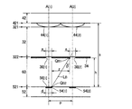
生体認証のために生体の静脈像を撮像する撮像装置が特許文献1に開示されている。図9に示すように、特許文献1の撮像装置は、複数の受光素子921が配列された受光部92と、各受光素子921に対応するレンズ(マイクロレンズ)941を含むレンズアレイ94と、受光部92とレンズアレイ94との間に介在する遮光層96とを具備する。遮光層96は、遮光性の板状部材で構成され、各受光素子921に対応する円筒状の開口部に光透過性の透光部961を充填した構造である。
An imaging apparatus that captures a vein image of a living body for biometric authentication is disclosed in
しかし、特許文献1の技術では、遮光層96の構造が複雑であるという問題がある。受光素子毎に開口部を有する薄膜状の遮光層が形成された基板を特許文献1の遮光層96の代わりに採用すれば構成は簡素化されるが、各レンズに対応する受光素子にそのレンズ以外からの光が到達するという問題(以下ではこの現象を「光線クロストーク」という)が顕在化する。以上の事情を考慮して、本発明は、光線クロストークを防止しながら撮像装置の構成を簡素化することを目的とする。
However, the technique of
以上の課題を解決するために、本発明の撮像装置は、第1面と第1面の反対側の第2面とを含む光透過性の第1基板(例えば基板32)と、第1面に沿って平面状に配置されて各々が入射光を集光する複数のレンズと、第2面に形成されて各レンズの光軸が通過する開口部を有する遮光層と、第2面に間隔をあけて対向する受光面をレンズの光軸が通過するように各レンズに対応して平面状に配置された複数の受光素子とを具備し、複数のレンズのうち相互に隣合う第1レンズ(例えばレンズ44[1])および第2レンズ(例えばレンズ44[2])の各々の光軸を通過する基準面内において、第1レンズの有効径の周縁(例えば点QA1)から第1レンズの光軸を通過して第1レンズに対応する受光素子の受光面の周縁(例えば点QA2)に至る直線(例えば直線LA)と第1基板の第2面との交点(例えば交点C1)で画定される基準領域の直径(例えば直径a0)を下回るように、第1レンズに対応する開口部の直径(例えば直径a)が設定され、かつ、基準面のうち第1レンズの光軸と第2レンズの軸との間の領域において、第2レンズに対応する開口部の周縁(例えば点QB1)と第1レンズに対応する受光素子の受光面の周縁(例えば点QB2)とを通過する直線(例えば直線LB)が第2レンズの光軸に対してなす角度(例えば角度θ)が、第1面に対する入射光の最大屈折角(例えば最大屈折角αm)を上回る。 In order to solve the above-described problems, an imaging apparatus according to the present invention includes a light-transmissive first substrate (for example, the substrate 32) including a first surface and a second surface opposite to the first surface, and a first surface. A plurality of lenses that are arranged in a plane along each of them and each collects incident light, a light-shielding layer that is formed on the second surface and has an opening through which the optical axis of each lens passes, and a distance between the second surfaces And a plurality of light receiving elements arranged in a plane corresponding to each lens so that the optical axis of the lens passes through the light receiving surfaces facing each other, and the first lenses adjacent to each other among the plurality of lenses (For example, the lens 44 [1]) and the second lens (for example, the lens 44 [2]), the first lens from the peripheral edge (for example, the point QA1) of the effective diameter of the first lens within the reference plane passing through the optical axis of each. A straight line that passes through the optical axis of the light receiving surface of the light receiving element corresponding to the first lens (for example, the point QA2) ( For example, the diameter of the opening corresponding to the first lens (for example, the diameter a0) is less than the diameter (for example, the diameter a0) of the reference region defined by the intersection (for example, the intersection C1) between the straight line LA) and the second surface of the first substrate. The diameter a) is set, and in the region between the optical axis of the first lens and the axis of the second lens in the reference plane, the periphery of the opening corresponding to the second lens (for example, the point QB1) and the first The angle (for example, angle θ) formed by the straight line (for example, straight line LB) passing through the peripheral edge (for example, point QB2) of the light receiving surface of the light receiving element corresponding to the lens with respect to the optical axis of the second lens is incident on the first surface. It exceeds the maximum refraction angle of light (for example, the maximum refraction angle αm).
以上の構成では、レンズ毎に開口部が形成された遮光層が第1基板の第2面に形成されるから、遮光性の板状部材の各開口部に透光部を挿入した特許文献1の構成と比較して、構成が簡素化されるという利点がある。また、第1レンズに対応する開口部の直径が基準領域の直径を下回る(第1条件)から、第1レンズに対応する開口部を通過する光のうち第1レンズ以外から到来した成分は、第1レンズに対応する受光素子の受光面に到達しない。更に、第2レンズに対応する開口部と第1レンズに対応する受光面とを結ぶ直線の角度が最大屈折角を上回る(第2条件)から、第2レンズに対応する開口部を通過した光は、第1レンズに対応する受光素子の受光面に到達しない。すなわち、各受光素子に対する光線クロストークを防止することが可能である。
In the above configuration, since the light shielding layer in which the opening is formed for each lens is formed on the second surface of the first substrate,
本発明の好適な態様において、各レンズの有効径Dと、遮光層の各開口部の直径aと、各受光素子の受光面と遮光層の表面との距離hと、各受光面の直径dと、各受光面と各レンズの中心との距離sとは、以下の数式(A)の関係を満たす。
a<(h・D+h・d−s・d)/s ……(A)
以上の構成では、撮像装置の各要素の寸法が数式(A)の関係を満たすから、第1レンズに対応する開口部を通過する光のうち第1レンズ以外から到来した成分は、第1レンズに対応する受光素子の受光面に到達しない。
In a preferred embodiment of the present invention, the effective diameter D of each lens, the diameter a of each opening of the light shielding layer, the distance h between the light receiving surface of each light receiving element and the surface of the light shielding layer, and the diameter d of each light receiving surface. The distance s between each light receiving surface and the center of each lens satisfies the relationship of the following formula (A).
a <(h · D + h · d−s · d) / s (A)
In the above configuration, since the dimensions of each element of the imaging device satisfy the relationship of the mathematical expression (A), the component that has arrived from other than the first lens in the light passing through the opening corresponding to the first lens is the first lens. Does not reach the light receiving surface of the light receiving element corresponding to.
本発明の好適な態様において、遮光層の各開口部の直径aと、複数の受光素子のピッチpと、各受光素子の受光面と遮光層の表面との距離hと、各受光面の直径dと、第1基板の屈折率nとは、以下の数式(B)の関係を満たす。
tan−1{(p−a/2−d/2)/h}>sin−1(1/n) ……(B)
以上の構成では、撮像装置の各要素の寸法が数式(B)の関係を満たすから、第2レンズに対応する開口部を通過した光は、第1レンズに対応する受光素子の受光面に到達しない。
In a preferred aspect of the present invention, the diameter a of each opening of the light shielding layer, the pitch p of the plurality of light receiving elements, the distance h between the light receiving surface of each light receiving element and the surface of the light shielding layer, and the diameter of each light receiving surface d and the refractive index n of the first substrate satisfy the relationship of the following mathematical formula (B).
tan −1 {(pa−2−d / 2) / h}> sin −1 (1 / n) (B)
In the above configuration, since the dimensions of each element of the imaging device satisfy the relationship of the formula (B), the light that has passed through the opening corresponding to the second lens reaches the light receiving surface of the light receiving element corresponding to the first lens. do not do.
本発明の好適な態様の撮像装置は、第1基板の第1面に間隔をあけて対向する第2基板(例えば基板42)を具備し、複数のレンズは、第2基板のうち第1基板との対向面(例えば表面421)に形成される。更に好適な態様において、第1基板と第2基板とは熱膨張率が相等しい。以上の態様では、第1基板と第2基板とで熱膨張率が共通するから、各レンズと各開口部との位置のずれや第1基板および第2基板の熱応力を防止することが可能である。他方、第1基板の第1面に複数のレンズを形成した構成(例えば後述の第2実施形態)では、撮像装置が薄型化されるという利点がある。 An imaging device according to a preferred aspect of the present invention includes a second substrate (for example, a substrate) facing the first surface of the first substrate with a space therebetween, and the plurality of lenses are the first substrate among the second substrates. Is formed on a surface facing the surface (for example, the surface 421). In a more preferred aspect, the first substrate and the second substrate have the same thermal expansion coefficient. In the above aspect, since the first substrate and the second substrate have the same coefficient of thermal expansion, it is possible to prevent displacement between the lenses and the openings and thermal stress of the first substrate and the second substrate. It is. On the other hand, a configuration in which a plurality of lenses are formed on the first surface of the first substrate (for example, a second embodiment described later) has an advantage that the imaging device is thinned.
本発明の好適な態様の撮像装置は、第1基板の第2面に間隔をあけて対向する第3基板(例えば基板52)を具備し、複数の受光素子は、第3基板のうち第1基板との対向面(例えば表面521)に形成される。更に好適な態様において、第1基板と第3基板とは熱膨張率が相等しい。以上の態様では、第1基板と第3基板とで熱膨張率が共通するから、各開口部と各受光素子との位置ずれや第1基板および第3基板の熱応力を防止することが可能である。 An image pickup apparatus according to a preferred aspect of the present invention includes a third substrate (for example, a substrate 52) facing the second surface of the first substrate with a space therebetween, and the plurality of light receiving elements are the first of the third substrates. It is formed on the surface facing the substrate (for example, the surface 521). In a more preferred aspect, the first substrate and the third substrate have the same coefficient of thermal expansion. In the above aspect, since the first substrate and the third substrate have the same coefficient of thermal expansion, it is possible to prevent displacement between the openings and the light receiving elements and thermal stress of the first substrate and the third substrate. It is.
本発明の好適な態様の撮像装置は、第2基板と第3基板との間に介在する光透過性の充填層を具備する。充填層の屈折率と第1基板の屈折率とを略一致させた構成によれば、第1基板に入射した光が第1基板と充填層との境界面(第2面)で直進するから、数式(B)を満たすように各要素の寸法を選定することで光線クロストークを有効に防止することが可能である。 The imaging device according to a preferred aspect of the present invention includes a light-transmitting filling layer interposed between the second substrate and the third substrate. According to the configuration in which the refractive index of the filling layer and the refractive index of the first substrate are substantially matched, the light incident on the first substrate travels straight at the boundary surface (second surface) between the first substrate and the filling layer. It is possible to effectively prevent light beam crosstalk by selecting the dimensions of each element so as to satisfy the mathematical formula (B).
<A:第1実施形態>
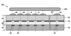
図1は、本発明の第1実施形態に係る撮像装置100の断面図であり、図2は、撮像装置100の分解断面図である。撮像装置100は、生体認証のために生体200(例えば人間の指)の静脈像を撮像する生体認証装置(静脈センサー)であり、図1および図2に示すように遮光基板30と集光基板40と受光基板50とを具備する。集光基板40は受光基板50と生体200(被写体)との間に介在し、遮光基板30は集光基板40と受光基板50との間に介在する。
<A: First Embodiment>
FIG. 1 is a cross-sectional view of the
遮光基板30は、基板32と遮光層34とを含んで構成される。基板32は、図2に示すように、集光基板40側の表面(以下「第1面」という)321と受光基板50側の表面(以下「第2面」という)322とを含む光透過性の板状部材である。例えばガラス基板が基板32として好適に利用される。遮光層34は、基板32の第2面322に形成された遮光性の薄膜である。図2に示すように、遮光層34には複数の開口部36が形成される。
The
集光基板40は、基板42と複数のレンズ(マイクロレンズ)44とを含んで構成される。基板42は、基板32と熱膨張率(線膨張係数)が等しい光透過性の板状部材である。基板42の厚さは0.5mm程度である。例えば遮光基板30の基板32と同様にガラス基板が基板42として好適に利用される。複数のレンズ44は、基板42のうち遮光基板30の第1面321に対向する表面421に形成されて行列状に配列する。各レンズ44は、生体200側からの入射光を集光する凸レンズである。なお、基板42と複数のレンズ44とを一体に形成することも可能である。レンズ44の曲率半径は例えば160μm程度に設定される。
The condensing
図1に示すように、複数のレンズ44の表面が遮光基板30の第1面321に対向および接触するように基板32と基板42との間隔が規定される。遮光層34の各開口部36は、集光基板40の各レンズ44に1対1に対応して形成された略円形の透光領域である。レンズ44の光軸はそのレンズ44に対応する開口部36の中心を通過する。
As shown in FIG. 1, the distance between the
受光基板50は、基板52と複数の受光素子54とを含んで構成される。基板52は、基板32および基板42と熱膨張率(線膨張係数)が等しい光透過性の板状部材である。例えば遮光基板30の基板32や集光基板40の基板42と同様にガラス基板が基板52として好適である。遮光基板30と受光基板50とは、両者間に充填された充填層60(接着剤)で相互に固定される。充填層60は、基板32と屈折率が等しい光透過性の材料(例えば樹脂材料)で形成される。
The
図2に示すように、複数の受光素子54は、基板52のうち遮光基板30の第2面322に対向する表面521に形成されて行列状に配列する。各受光素子54は、第2面322に対向する略円形の受光面56に入射する光量に応じた検出信号を生成する。集光基板40の各レンズ44と受光基板50の各受光素子54とは1対1に対応する。具体的には、レンズ44の光軸はそのレンズ44に対応する受光素子54の受光面56の中心を通過する。なお、受光基板50の製造には、例えば2009−200104号公報に開示された技術を利用できる。
As shown in FIG. 2, the plurality of light receiving
以上の構成において、図1に矢印で示すように、所定の位置(例えば生体200を挟んで集光基板40とは反対側)に配置された光源(図示略)による照射光が生体200の内部の静脈にて透過または反射して集光基板40に入射し、各レンズ44で集光されたうえで遮光層34の開口部36を通過して受光素子54の受光面56に到達する。すなわち、生体200の静脈像が撮像される。遮光層34の各開口部36は、その開口部36に対応する受光素子54に対する入射光を制限する手段として機能する。
In the above configuration, as indicated by an arrow in FIG. 1, light emitted from a light source (not shown) disposed at a predetermined position (for example, on the side opposite to the condensing
以上の構成によれば、受光素子54毎に開口部36を形成した遮光層34が基板32の第2面322に形成されるから、遮光性の板状部材の開口部に透光部961を充填した図9の遮光層34を採用する特許文献1の技術と比較して撮像装置100の構成が簡素化されるという利点がある。
According to the above configuration, since the
ところで、特許文献1の技術では、受光部92がシリコンで形成され、レンズアレイ94が石英ガラスで形成され、遮光層96が樹脂材料で形成される。すなわち、各要素の熱膨張率が大幅に相違する。したがって、例えばレンズ941と遮光層96の透光部961と受光素子921との各位置を高い精度で整合させることが困難であるという問題がある。また、熱膨張率の相違に起因した熱応力が各要素に発生するという問題もある。他方、第1実施形態では、基板32と基板42と基板52とで熱膨張率が共通するから、レンズ44と開口部36と受光素子54との位置の誤差を防止するとともに、各要素(集光基板40,遮光基板30,受光基板50)における熱応力の発生を抑制できるという利点がある。もっとも、熱膨張率の相違が問題とならないのであれば、基板32と基板42との熱膨張率を相違させた構成や、基板42と基板52との熱膨張率を相違させた構成も採用され得る
By the way, in the technique of
撮像装置100の各要素の寸法は、光線クロストークが防止されるように選定される。図3および図4に示すように、集光基板40の複数のレンズ44のうち任意の1個のレンズ44[1]とレンズ44[1]に隣接する1個のレンズ44[2]とに着目して各要素の寸法の条件を詳述する。以下の説明では、レンズ44[1]に対応する要素(光軸A,開口部36,受光素子54,受光面56)の符号に便宜的に添字[1]を付加し、レンズ44[2]に対応する要素の符号には添字[2]を付加する。図3および図4は、レンズ44[1]の光軸A[1]とレンズ44[2]の光軸A[2]とを通過する平面(以下「基準面」という)での撮像装置100の断面図である。なお、図3および図4では、図面の煩雑化を防止する趣旨から各要素のハッチングを省略した。
The dimensions of each element of the
撮像装置100の各要素の寸法は、光線クロストークを防止するための第1条件(図3)と第2条件(図4)とを満たすように選定される。第1条件は、開口部36[1]を通過する光のうちレンズ44[1]を透過した光のみが受光素子54[1]の受光面56[1]に入射する(すなわち、レンズ44[1]以外から到来して開口部36[1]を通過した光は受光面56[1]の外側に到達する)という条件である。第2条件は、開口部36[2]を透過した光が受光素子54[1]の受光面56[1]に入射しない(受光面56[1]の外側に到達する)という条件である。第1条件および第2条件の各々について以下に詳述する。
The dimensions of each element of the
<第1条件>
図3に示すように、基準面内に直線LAを想定する。直線LAは、レンズ44[1]の周縁上の点QA1からレンズ44[1]の光軸A[1]と交差して受光素子54[1]の受光面56[1]の周縁上の点QA2に至る直線である。点QA1と点QA2とは、基準面内で光軸A[1]を挟んで反対側に位置する。直線LAと遮光基板30の基板32の第2面322との交点C1により基準領域Rが画定される。すなわち、基準領域Rは、第2面322と光軸A[1]との交点C0を中心として交点C1を円周上の点とする直径a0の円形領域である。基準領域Rの直径a0は、交点C0と交点C1との距離(すなわち半径)の2倍に相当する。
<First condition>
As shown in FIG. 3, a straight line LA is assumed in the reference plane. The straight line LA intersects with the optical axis A [1] of the lens 44 [1] from the point QA1 on the periphery of the lens 44 [1] and points on the periphery of the light receiving surface 56 [1] of the light receiving element 54 [1]. A straight line leading to QA2. The points QA1 and QA2 are located on opposite sides of the optical axis A [1] in the reference plane. A reference region R is defined by an
図3から理解されるように、開口部36[1]の直径aが基準領域Rの直径a0を下回るように各開口部36の直径aを選定すれば(a<a0)、レンズ44[1]以外の領域から到来して開口部36[1]を通過した光は受光面56[1]の外側に到達する。すなわち、第1条件が満たされる。
As understood from FIG. 3, if the diameter a of each
図3から幾何学的に把握される通り、基準領域Rの直径a0と、受光面56[1]の直径dと、受光面56[1](基板52の表面521)と遮光層34の表面との距離hと、光軸A[1]に沿う距離xとは、以下の数式(a1)の条件を満たす。距離xは、図3に示すように、直線LAと光軸A[1]との交点C2から受光面56[1]までの距離である。
a0/(h−x)=d/x ……(a1)
数式(a1)から以下の数式(a2)が導出される。
a0=d(h−x)/x ……(a2)
As geometrically understood from FIG. 3, the diameter a0 of the reference region R, the diameter d of the light receiving surface 56 [1], the light receiving surface 56 [1] (the
a0 / (h-x) = d / x (a1)
The following formula (a2) is derived from the formula (a1).
a0 = d (h−x) / x (a2)
また、レンズ44[1]の直径(有効径)Dと、受光面56[1]とレンズ44[1]の中心(基板42の表面421)との距離sは以下の数式(a3)を満たす。
D/(s−x)=d/x ……(a3)
数式(a3)から以下の数式(a4)が導出される。
x=d・s/(D+d) ……(a4)
The diameter (effective diameter) D of the lens 44 [1] and the distance s between the light receiving surface 56 [1] and the center of the lens 44 [1] (the
D / (s−x) = d / x (a3)
The following formula (a4) is derived from the formula (a3).
x = d · s / (D + d) (a4)
数式(a4)を数式(a1)に代入することで以下の数式(a5)が導出される。
a0=(h・D+h・d−s・d)/s ……(a5)
開口部36[1]の直径aが基準領域Rの直径a0を下回る(a<a0)という前述の条件と数式(a5)とから、第1条件を表現する以下の数式(A)が導出される。遮光層34の各開口部36の直径aは、数式(A)を満たすように選定される。
a<(h・D+h・d−s・d)/s ……(A)
By substituting equation (a4) into equation (a1), the following equation (a5) is derived.
a0 = (h.D + h.d-s.d) / s (a5)
From the above condition that the diameter a of the opening 36 [1] is smaller than the diameter a0 of the reference region R (a <a0) and the expression (a5), the following expression (A) expressing the first condition is derived. The The diameter a of each opening 36 of the
a <(h · D + h · d−s · d) / s (A)
<第2条件>
図4に示すように、基準面内に直線LBを想定する。直線LBは、レンズ44[1]の光軸A[1]とレンズ44[2]の光軸A[2]との間の領域において、開口部36[2]の周縁上の点QB1と受光素子54[1]の受光面56[1]の周縁上の点QB2とを通過する直線である。直線LBは、レンズ44[2]の光軸A[2]に対して角度θをなす。
<Second condition>
As shown in FIG. 4, a straight line LB is assumed in the reference plane. The straight line LB is received by the point QB1 on the periphery of the opening 36 [2] and the light reception in the region between the optical axis A [1] of the lens 44 [1] and the optical axis A [2] of the lens 44 [2]. This is a straight line passing through the point QB2 on the periphery of the light receiving surface 56 [1] of the element 54 [1]. The straight line LB forms an angle θ with respect to the optical axis A [2] of the lens 44 [2].
図4から理解されるように、直線LBの角度θが、開口部36[2]を通過して充填層60の内部を進行する光が光軸A[2]に対してなす角度αの最大値(以下「最大屈折角」という)αmを上回れば(θ>αm)、開口部36[2]を通過した光は受光面56[1]には到達しない。すなわち、第2条件が満たされる。
As understood from FIG. 4, the angle θ of the straight line LB is the maximum of the angle α that the light traveling through the
図5に示すように、遮光基板30の基板32の第1面321に入射角αinで空気中から光が入射した場合を想定する。入射角αinと第1面321での屈折角αとの関係は、基板32の屈折率nを含む以下の数式(b1)で表現される。
sin(α)=sin(αin)/n ……(b1)
As shown in FIG. 5, it is assumed that light is incident on the
sin (α) = sin (αin) / n (b1)
充填層60の屈折率が基板32の屈折率nと同等であると仮定すると、基板32の第1面321に入射した光は、基板32と充填層60との境界面(第2面322)にて直進し、数式(b1)を満たす屈折角αで充填層60の内部を透過する。充填層60の内部での最大屈折角αmは、数式(b1)の入射角αinを90°とした場合に相当するから(sin(αm)=sin(90°)/n)、最大屈折角αmを表現する以下の数式(b2)が導出される。
αm=sin−1(1/n) ……(b2)
Assuming that the refractive index of the
αm = sin −1 (1 / n) (b2)
他方、図4から幾何学的に把握される通り、第2面322に平行な方向における点QB1と点QB2との距離zは、以下の数式(b3)で表現される。数式(b3)の記号pは、受光素子54[1]と受光素子54[2]とのピッチ(すなわち受光面56[1]と受光面56[2]との中心間距離)を意味する。
z=p−a/2−d/2 ……(b3)
したがって、直線LBと光軸[2]との角度θは、距離zと前述の距離h(受光面56[2]と遮光層34の表面との距離)とを含む以下の数式(b4)を満たす。
tan(θ)=z/h
=(p−a/2−d/2)/h ……(b4)
数式(b4)から以下の数式(b5)が導出される。
θ=tan−1{(p−a/2−d/2)/h} ……(b5)
On the other hand, as geometrically understood from FIG. 4, the distance z between the point QB1 and the point QB2 in the direction parallel to the
z = pa / 2-d / 2 (b3)
Therefore, the angle θ between the straight line LB and the optical axis [2] is expressed by the following formula (b4) including the distance z and the above-described distance h (the distance between the light receiving surface 56 [2] and the surface of the light shielding layer 34). Fulfill.
tan (θ) = z / h
= (Pa-2−d / 2) / h (b4)
The following formula (b5) is derived from the formula (b4).
θ = tan −1 {(pa−2−d / 2) / h} (b5)
直線LBの角度θが最大屈折角αmを上回る(θ>αm)という前述の条件と数式(b2)および数式(b5)とから、第2条件を表現する以下の数式(B)が導出される。
tan−1{(p−a/2−d/2)/h}>sin−1(1/n) ……(B)
From the above-mentioned condition that the angle θ of the straight line LB exceeds the maximum refraction angle αm (θ> αm) and the equations (b2) and (b5), the following equation (B) expressing the second condition is derived. .
tan −1 {(pa−2−d / 2) / h}> sin −1 (1 / n) (B)
撮像装置100の各要素の寸法は、数式(A)および数式(B)を満たすように選定される。したがって、レンズ44[1]以外から到来して開口部36[1]を通過した光は受光面56[1]に入射せず(数式(A):第1条件)、かつ、開口部36[2]を通過した光は受光面56[1]に入射しない(数式(B):第2条件)。すなわち、第1実施形態によれば、各受光素子54に対する光線クロストークを防止することが可能である。
The dimension of each element of the
例えば、レンズ44の直径Dと受光素子54のピッチpと距離hとを100μmとし、受光素子54の直径dを10μmとし、距離sを400μmとした場合、数式(A)の右辺は17.5μmとなる。したがって、各開口部36の直径aは、数式(A)を満たす範囲内で例えば15μmに設定される。また、以上の条件のもとでは角度θ(数式(B)の左辺)は約41.19°となる。基板32および充填層60の屈折率nを1.53とした場合、最大屈折角αm(数式(B)の右辺)は約40.81°となるから、数式(B)の条件を満たす。以上のように数式(A)および数式(B)の双方を満たすから、各受光素子54に対する光線クロストークを防止することが可能である。
For example, when the diameter D of the
<B:第2実施形態>
本発明の第2実施形態を以下に説明する。なお、以下に例示する各構成において作用や機能が第1実施形態と同等である要素については、以上の説明で参照した符号を流用して各々の詳細な説明を適宜に省略する。
<B: Second Embodiment>
A second embodiment of the present invention will be described below. In addition, about the element in which an effect | action and a function are equivalent to 1st Embodiment in each structure illustrated below, the detailed description of each is abbreviate | omitted suitably using the code | symbol referred by the above description.
図6は、第2実施形態の撮像装置100の断面図である。図6に示すように、第2実施形態の撮像装置100では、遮光基板30の基板32のうち生体200側の第1面321に複数のレンズ44が形成される。各レンズ44は、第1実施形態と同様に、生体200から到来する光を集光する。
FIG. 6 is a cross-sectional view of the
第2実施形態においても第1条件と第2条件とを満たすように撮像装置100の各要素の寸法が選定される。したがって、第1実施形態と同様の効果が実現される。また、第2実施形態では、複数のレンズ44が基板32に形成されるから、第1実施形態の基板32は不要である。したがって、第1実施形態と比較して撮像装置100を薄型化することが可能である。
Also in the second embodiment, the dimensions of each element of the
<C:第3実施形態>
図7は、第3実施形態の撮像装置100の断面図である。図7に示すように、第3実施形態の撮像装置100は、基板42と複数のレンズ44との間に介在する遮光層46を集光基板40に追加した構成である。遮光層46には、各レンズ44に対応する円形の開口部461が形成される。生体200から基板42に入射した光のうち開口部461を通過した光が各レンズ44で集光される。
<C: Third Embodiment>
FIG. 7 is a cross-sectional view of the
第3実施形態における数式(A)の寸法Dは、遮光層46の開口部461の直径である。すなわち、第1実施形態におけるレンズ44の直径と第3実施形態の開口部461の直径とは、レンズ44の有効径Dとして包括される。第3実施形態においても第1実施形態と同様の効果が実現される。
The dimension D of the mathematical formula (A) in the third embodiment is the diameter of the
<D:第4実施形態>
図8は、第4実施形態の撮像装置100の断面図である。図8に示すように、第4実施形態の撮像装置100は、基板52の表面521を覆う遮光層58を受光基板50に追加した構成である。遮光層58には、各受光素子54に対応する円形の開口部581が形成される。基板32および充填層60を透過した光は開口部581を通過して受光素子54に入射する。
<D: Fourth Embodiment>
FIG. 8 is a cross-sectional view of the
第4実施形態における数式(A)および数式(B)の寸法dは、遮光層58の開口部581の直径である。すなわち、受光素子54の表面のうち開口部581の内側に露出する領域が受光面56として機能する。第4実施形態においても第1実施形態と同様の効果が実現される。
The dimension d in the mathematical expressions (A) and (B) in the fourth embodiment is the diameter of the
100……撮像装置、200……生体、30……遮光基板、32……基板(第1基板)、321……第1面、322……第2面、34……遮光層、36……開口部、40……集光基板、42……基板(第2基板)、44……レンズ、46……遮光層、461……開口部、50……受光基板、52……基板(第3基板)、54……受光素子、56……受光面、58……遮光層、581……開口部、60……充填層。
DESCRIPTION OF
Claims (9)
前記第1面に沿って平面状に配置されて各々が入射光を集光する複数のレンズと、
前記第2面に形成されて前記各レンズの光軸が通過する開口部を有する遮光層と、
前記第2面に間隔をあけて対向する受光面を前記レンズの光軸が通過するように前記各レンズに対応して平面状に配置された複数の受光素子とを具備し、
前記複数のレンズのうち相互に隣合う第1レンズおよび第2レンズの各々の光軸を通過する基準面内において、前記第1レンズの有効径の周縁から前記第1レンズの光軸を通過して前記第1レンズに対応する前記受光素子の前記受光面の周縁に至る直線と前記第1基板の前記第2面との交点で画定される基準領域の直径を下回るように、前記各レンズの有効径Dと、前記遮光層の前記各開口部の直径aと、前記各受光素子の前記受光面と前記遮光層の表面との距離hと、前記各受光面の直径dと、前記各受光面と前記各レンズの中心との距離sとが、以下の数式(A)の関係を満たす条件のもとで、前記第1レンズに対応する前記開口部の直径が設定され、
a<(h・D+h・d−s・d)/s ……(A)
かつ、前記基準面のうち前記第1レンズの光軸と前記第2レンズの軸との間の領域において、前記第2レンズに対応する前記開口部の周縁と前記第1レンズに対応する前記受光素子の前記受光面の周縁とを通過する直線が前記第2レンズの光軸に対してなす角度が、前記第1面に対する入射光の最大屈折角を上回るように、前記遮光層の前記各開口部の直径aと、前記複数の受光素子のピッチpと、前記各受光素子の前記受光面と前記遮光層の表面との距離hと、前記各受光面の直径dと、前記第1基板の屈折率nとは、以下の数式(B)の関係を満たす
tan −1 {(p−a/2−d/2)/h}>sin −1 (1/n) ……(B)
撮像装置。 A light transmissive first substrate including a first surface and a second surface opposite to the first surface;
A plurality of lenses arranged in a planar shape along the first surface, each of which collects incident light;
A light shielding layer formed on the second surface and having an opening through which an optical axis of each lens passes;
A plurality of light receiving elements arranged in a plane corresponding to each lens such that the optical axis of the lens passes through a light receiving surface facing the second surface with a space therebetween;
The reference lens passes through the optical axis of the first lens from the periphery of the effective diameter of the first lens in a reference plane that passes through the optical axes of the first lens and the second lens adjacent to each other among the plurality of lenses. Each of the lenses so as to be less than a diameter of a reference region defined by an intersection of a straight line extending to the periphery of the light receiving surface of the light receiving element corresponding to the first lens and the second surface of the first substrate. Effective diameter D, diameter a of each opening of the light shielding layer, distance h between the light receiving surface of each light receiving element and the surface of the light shielding layer, diameter d of each light receiving surface, and each light receiving The diameter of the opening corresponding to the first lens is set under the condition that the distance s between the surface and the center of each lens satisfies the relationship of the following formula (A):
a <(h · D + h · d−s · d) / s (A)
And in the region between the optical axis of the first lens and the axis of the second lens in the reference plane, the periphery of the opening corresponding to the second lens and the light reception corresponding to the first lens Each opening of the light shielding layer so that an angle formed by a straight line passing through the periphery of the light receiving surface of the element with respect to the optical axis of the second lens exceeds a maximum refraction angle of incident light with respect to the first surface. Diameter a, a pitch p of the plurality of light receiving elements, a distance h between the light receiving surface of each light receiving element and the surface of the light shielding layer, a diameter d of each light receiving surface, and the first substrate The refractive index n satisfies the relationship of the following formula (B).
tan −1 {(pa−2−d / 2) / h}> sin −1 (1 / n) (B)
Imaging device.
前記複数のレンズは、前記第2基板のうち前記第1基板との対向面に形成される
請求項1の撮像装置。 Comprising a second substrate facing the first surface of the first substrate with a gap therebetween;
The plurality of lenses are formed on a surface of the second substrate facing the first substrate.
The imaging device according to claim 1 .
請求項2の撮像装置。 The first substrate and the second substrate have the same coefficient of thermal expansion.
The imaging device according to claim 2 .
請求項1の撮像装置。 The plurality of lenses are formed on the first surface of the first substrate.
The imaging device according to claim 1 .
前記第1基板の前記第1面に間隔をあけて対向する第2基板と、
前記第2基板のうち前記第1基板との対向面に記第1面に沿って平面状に配置されて各々が入射光を集光する複数のレンズと、
前記第2面に形成されて前記各レンズの光軸が通過する開口部を有する遮光層と、
前記第2面に間隔をあけて対向する受光面を前記レンズの光軸が通過するように前記各レンズに対応して平面状に配置された複数の受光素子とを具備し、
前記複数のレンズのうち相互に隣合う第1レンズおよび第2レンズの各々の光軸を通過する基準面内において、前記第1レンズの有効径の周縁から前記第1レンズの光軸を通過して前記第1レンズに対応する前記受光素子の前記受光面の周縁に至る直線と前記第1基板の前記第2面との交点で画定される基準領域の直径を下回るように、前記各レンズの有効径Dと、前記遮光層の前記各開口部の直径aと、前記各受光素子の前記受光面と前記遮光層の表面との距離hと、前記各受光面の直径dと、前記各受光面と前記各レンズの中心との距離sとが、以下の数式(A)の関係を満たす条件のもとで、前記第1レンズに対応する前記開口部の直径が設定され、
a<(h・D+h・d−s・d)/s ……(A)
かつ、前記基準面のうち前記第1レンズの光軸と前記第2レンズの軸との間の領域において、前記第2レンズに対応する前記開口部の周縁と前記第1レンズに対応する前記受光素子の前記受光面の周縁とを通過する直線が前記第2レンズの光軸に対してなす角度が、前記第1面に対する入射光の最大屈折角を上回り、
前記第1基板と前記第2基板とは熱膨張率が相等しい
撮像装置。 A light transmissive first substrate including a first surface and a second surface opposite to the first surface;
A second substrate facing the first surface of the first substrate with a gap therebetween;
A plurality of lenses arranged in a plane along the first surface on the surface facing the first substrate of the second substrate, each of which collects incident light;
A light shielding layer formed on the second surface and having an opening through which an optical axis of each lens passes;
A plurality of light receiving elements arranged in a plane corresponding to each lens such that the optical axis of the lens passes through a light receiving surface facing the second surface with a space therebetween;
The reference lens passes through the optical axis of the first lens from the periphery of the effective diameter of the first lens in a reference plane that passes through the optical axes of the first lens and the second lens adjacent to each other among the plurality of lenses. Each of the lenses so as to be less than a diameter of a reference region defined by an intersection of a straight line extending to the periphery of the light receiving surface of the light receiving element corresponding to the first lens and the second surface of the first substrate. Effective diameter D, diameter a of each opening of the light shielding layer, distance h between the light receiving surface of each light receiving element and the surface of the light shielding layer, diameter d of each light receiving surface, and each light receiving The diameter of the opening corresponding to the first lens is set under the condition that the distance s between the surface and the center of each lens satisfies the relationship of the following formula (A):
a <(h · D + h · d−s · d) / s (A)
And in the region between the optical axis of the first lens and the axis of the second lens in the reference plane, the periphery of the opening corresponding to the second lens and the light reception corresponding to the first lens angle formed with respect to the optical axis of said the straight line passing through the periphery of the light receiving surface and the second lens element, Ri exceeded the maximum refraction angle of the light incident on the first surface,
An imaging apparatus in which the first substrate and the second substrate have the same thermal expansion coefficient .
前記複数の受光素子は、前記第3基板のうち前記第1基板との対向面に形成される
請求項1から請求項5の何れかの撮像装置。 Comprising a third substrate facing the second surface of the first substrate with a gap therebetween;
The imaging device according to claim 1, wherein the plurality of light receiving elements are formed on a surface of the third substrate facing the first substrate.
前記第1基板の前記第2面に間隔をあけて対向する第3基板と、
前記第1面に沿って平面状に配置されて各々が入射光を集光する複数のレンズと、
前記第2面に形成されて前記各レンズの光軸が通過する開口部を有する遮光層と、
前記第2面に間隔をあけて対向する受光面を前記レンズの光軸が通過するように、前記第3基板のうち前記第1基板との対向面に、前記各レンズに対応して平面状に配置された複数の受光素子とを具備し、
前記複数のレンズのうち相互に隣合う第1レンズおよび第2レンズの各々の光軸を通過する基準面内において、前記第1レンズの有効径の周縁から前記第1レンズの光軸を通過して前記第1レンズに対応する前記受光素子の前記受光面の周縁に至る直線と前記第1基板の前記第2面との交点で画定される基準領域の直径を下回るように、前記各レンズの有効径Dと、前記遮光層の前記各開口部の直径aと、前記各受光素子の前記受光面と前記遮光層の表面との距離hと、前記各受光面の直径dと、前記各受光面と前記各レンズの中心との距離sとが、以下の数式(A)の関係を満たす条件のもとで、前記第1レンズに対応する前記開口部の直径が設定され、
a<(h・D+h・d−s・d)/s ……(A)
かつ、前記基準面のうち前記第1レンズの光軸と前記第2レンズの軸との間の領域において、前記第2レンズに対応する前記開口部の周縁と前記第1レンズに対応する前記受光素子の前記受光面の周縁とを通過する直線が前記第2レンズの光軸に対してなす角度が、前記第1面に対する入射光の最大屈折角を上回り、
前記第1基板と前記第3基板とは熱膨張率が相等しい
撮像装置。 A light transmissive first substrate including a first surface and a second surface opposite to the first surface;
A third substrate facing the second surface of the first substrate with a gap therebetween;
A plurality of lenses arranged in a planar shape along the first surface, each of which collects incident light;
A light shielding layer formed on the second surface and having an opening through which an optical axis of each lens passes;
The surface of the third substrate facing the first substrate is planar so as to correspond to each lens so that the optical axis of the lens passes through the light receiving surface facing the second surface with a space therebetween. And a plurality of light receiving elements arranged in
The reference lens passes through the optical axis of the first lens from the periphery of the effective diameter of the first lens in a reference plane that passes through the optical axes of the first lens and the second lens adjacent to each other among the plurality of lenses. Each of the lenses so as to be less than a diameter of a reference region defined by an intersection of a straight line extending to the periphery of the light receiving surface of the light receiving element corresponding to the first lens and the second surface of the first substrate. Effective diameter D, diameter a of each opening of the light shielding layer, distance h between the light receiving surface of each light receiving element and the surface of the light shielding layer, diameter d of each light receiving surface, and each light receiving The diameter of the opening corresponding to the first lens is set under the condition that the distance s between the surface and the center of each lens satisfies the relationship of the following formula (A):
a <(h · D + h · d−s · d) / s (A)
And in the region between the optical axis of the first lens and the axis of the second lens in the reference plane, the periphery of the opening corresponding to the second lens and the light reception corresponding to the first lens angle formed with respect to the optical axis of said the straight line passing through the periphery of the light receiving surface and the second lens element, Ri exceeded the maximum refraction angle of the light incident on the first surface,
An imaging apparatus in which the first substrate and the third substrate have the same thermal expansion coefficient .
を具備する請求項6または請求項7の撮像装置。 The imaging device according to claim 6, further comprising a light-transmitting filling layer interposed between the plurality of lenses and the plurality of light receiving elements .
前記第1基板の前記第1面に間隔をあけて対向する第2基板と、
前記第2基板のうち前記第1基板との対向面に前記第1面に沿って平面状に配置されて各々が入射光を集光する複数のレンズと、
前記第1基板の前記第2面に間隔をあけて対向する第3基板と、
前記第2面に形成されて前記各レンズの光軸が通過する開口部を有する遮光層と、
前記第2面に間隔をあけて対向する受光面を前記レンズの光軸が通過するように、前記第3基板のうち前記第1基板との対向面に、前記各レンズに対応して平面状に配置された複数の受光素子と、
前記第2基板と前記第3基板との間に介在する光透過性の充填層とを具備し、
前記複数のレンズのうち相互に隣合う第1レンズおよび第2レンズの各々の光軸を通過する基準面内において、前記第1レンズの有効径の周縁から前記第1レンズの光軸を通過して前記第1レンズに対応する前記受光素子の前記受光面の周縁に至る直線と前記第1基板の前記第2面との交点で画定される基準領域の直径を下回るように、前記各レンズの有効径Dと、前記遮光層の前記各開口部の直径aと、前記各受光素子の前記受光面と前記遮光層の表面との距離hと、前記各受光面の直径dと、前記各受光面と前記各レンズの中心との距離sとが、以下の数式(A)の関係を満たす条件のもとで、前記第1レンズに対応する前記開口部の直径が設定され、
a<(h・D+h・d−s・d)/s ……(A)
かつ、前記基準面のうち前記第1レンズの光軸と前記第2レンズの軸との間の領域において、前記第2レンズに対応する前記開口部の周縁と前記第1レンズに対応する前記受光素子の前記受光面の周縁とを通過する直線が前記第2レンズの光軸に対してなす角度が、前記第1面に対する入射光の最大屈折角を上回り、
前記充填層の屈折率と前記第1基板の屈折率とは相等しい
撮像装置。 A light transmissive first substrate including a first surface and a second surface opposite to the first surface;
A second substrate facing the first surface of the first substrate with a gap therebetween;
A plurality of lenses arranged in a plane along the first surface on the surface of the second substrate facing the first substrate, each of which collects incident light;
A third substrate facing the second surface of the first substrate with a gap therebetween;
A light shielding layer formed on the second surface and having an opening through which an optical axis of each lens passes;
The surface of the third substrate facing the first substrate is planar so as to correspond to each lens so that the optical axis of the lens passes through the light receiving surface facing the second surface with a space therebetween. a plurality of light receiving elements arranged in,
Comprising a light-transmitting filling layer interposed between the second substrate and the third substrate ;
The reference lens passes through the optical axis of the first lens from the periphery of the effective diameter of the first lens in a reference plane that passes through the optical axes of the first lens and the second lens adjacent to each other among the plurality of lenses. Each of the lenses so as to be less than a diameter of a reference region defined by an intersection of a straight line extending to the periphery of the light receiving surface of the light receiving element corresponding to the first lens and the second surface of the first substrate. Effective diameter D, diameter a of each opening of the light shielding layer, distance h between the light receiving surface of each light receiving element and the surface of the light shielding layer, diameter d of each light receiving surface, and each light receiving The diameter of the opening corresponding to the first lens is set under the condition that the distance s between the surface and the center of each lens satisfies the relationship of the following formula (A):
a <(h · D + h · d−s · d) / s (A)
And in the region between the optical axis of the first lens and the axis of the second lens in the reference plane, the periphery of the opening corresponding to the second lens and the light reception corresponding to the first lens angle formed with respect to the optical axis of said the straight line passing through the periphery of the light receiving surface and the second lens element, Ri exceeded the maximum refraction angle of the light incident on the first surface,
An imaging device in which a refractive index of the filling layer is equal to a refractive index of the first substrate .
Priority Applications (3)
| Application Number | Priority Date | Filing Date | Title |
|---|---|---|---|
| JP2011063926A JP5742348B2 (en) | 2011-03-23 | 2011-03-23 | Imaging device |
| US13/421,295 US8665357B2 (en) | 2011-03-23 | 2012-03-15 | Imaging apparatus |
| CN201210076879.9A CN102842027B (en) | 2011-03-23 | 2012-03-21 | Camera head |
Applications Claiming Priority (1)
| Application Number | Priority Date | Filing Date | Title |
|---|---|---|---|
| JP2011063926A JP5742348B2 (en) | 2011-03-23 | 2011-03-23 | Imaging device |
Related Child Applications (1)
| Application Number | Title | Priority Date | Filing Date |
|---|---|---|---|
| JP2015093171A Division JP2015173474A (en) | 2015-04-30 | 2015-04-30 | Imaging apparatus |
Publications (3)
| Publication Number | Publication Date |
|---|---|
| JP2012199868A JP2012199868A (en) | 2012-10-18 |
| JP2012199868A5 JP2012199868A5 (en) | 2014-05-08 |
| JP5742348B2 true JP5742348B2 (en) | 2015-07-01 |
Family
ID=46877065
Family Applications (1)
| Application Number | Title | Priority Date | Filing Date |
|---|---|---|---|
| JP2011063926A Expired - Fee Related JP5742348B2 (en) | 2011-03-23 | 2011-03-23 | Imaging device |
Country Status (3)
| Country | Link |
|---|---|
| US (1) | US8665357B2 (en) |
| JP (1) | JP5742348B2 (en) |
| CN (1) | CN102842027B (en) |
Families Citing this family (21)
| Publication number | Priority date | Publication date | Assignee | Title |
|---|---|---|---|---|
| JP6074981B2 (en) | 2012-09-26 | 2017-02-08 | セイコーエプソン株式会社 | Imaging device |
| JP6044239B2 (en) | 2012-10-01 | 2016-12-14 | セイコーエプソン株式会社 | Imaging device and medical device |
| US9692251B2 (en) | 2014-07-03 | 2017-06-27 | Intel Corporation | Apparatus, system and method of wireless power transfer |
| JP2016115862A (en) * | 2014-12-17 | 2016-06-23 | セイコーエプソン株式会社 | Image acquisition device, biological information acquisition device, electronic apparatus |
| CN107451518A (en) * | 2016-05-30 | 2017-12-08 | 深圳印象认知技术有限公司 | A kind of display screen |
| CN106022324B (en) | 2016-08-04 | 2019-04-30 | 京东方科技集团股份有限公司 | A kind of lines identification display device |
| CN108573191B (en) * | 2017-03-07 | 2021-12-17 | 固安翌光科技有限公司 | OLED screen body used as light source of fingerprint identification device and optical fingerprint identification device |
| CN106886341B (en) * | 2017-03-28 | 2022-02-25 | 京东方科技集团股份有限公司 | Display substrate and display device |
| CN106971173B (en) * | 2017-04-13 | 2021-01-26 | 京东方科技集团股份有限公司 | Touch substrate and display panel |
| KR102350605B1 (en) * | 2017-04-17 | 2022-01-14 | 삼성전자주식회사 | Image sensor |
| FR3075466B1 (en) * | 2017-12-15 | 2020-05-29 | Stmicroelectronics (Grenoble 2) Sas | ELECTRONIC CIRCUIT BOX COVER |
| FR3075465B1 (en) | 2017-12-15 | 2020-03-27 | Stmicroelectronics (Grenoble 2) Sas | ELECTRONIC CIRCUIT BOX COVER |
| SE1751613A1 (en) * | 2017-12-21 | 2019-06-22 | Fingerprint Cards Ab | Biometric imaging device and method for manufacturing the biometric imaging device |
| WO2020061823A1 (en) * | 2018-09-26 | 2020-04-02 | 深圳市汇顶科技股份有限公司 | Optical image acquisition unit, optical image acquisition apparatus and electronic device |
| JP7293791B2 (en) * | 2019-03-26 | 2023-06-20 | 富士フイルムビジネスイノベーション株式会社 | Optical device, image reading device, and image forming device |
| CN110471572B (en) * | 2019-06-10 | 2021-09-10 | 惠科股份有限公司 | Display device and touch controller |
| US11844236B2 (en) | 2019-07-12 | 2023-12-12 | Semiconductor Energy Laboratory Co., Ltd. | Functional panel, display device, input/output device, and data processing device |
| KR20220035438A (en) * | 2019-07-23 | 2022-03-22 | 쓰리엠 이노베이티브 프로퍼티즈 컴파니 | Optical system including microlens and light blocking structure |
| JP6835920B2 (en) * | 2019-08-23 | 2021-02-24 | 浜松ホトニクス株式会社 | Photodetector |
| WO2021176704A1 (en) * | 2020-03-06 | 2021-09-10 | オリンパス株式会社 | Optical unit, optical-unit manufacturing method, and endoscope |
| CN114255673A (en) * | 2021-12-31 | 2022-03-29 | 浙江全视通科技有限公司 | Process-optimized under-screen camera device |
Family Cites Families (13)
| Publication number | Priority date | Publication date | Assignee | Title |
|---|---|---|---|---|
| JPH09171154A (en) * | 1995-12-19 | 1997-06-30 | Nippon Sheet Glass Co Ltd | Image input optical system and image input device using the same |
| US6995800B2 (en) * | 2000-01-27 | 2006-02-07 | Canon Kabushiki Kaisha | Image pickup apparatus utilizing a plurality of converging lenses |
| US7068432B2 (en) * | 2004-07-27 | 2006-06-27 | Micron Technology, Inc. | Controlling lens shape in a microlens array |
| JP5007082B2 (en) | 2006-08-04 | 2012-08-22 | 日立マクセル株式会社 | Imaging device and biometric authentication device |
| US7728902B2 (en) | 2006-08-04 | 2010-06-01 | Hitachi Maxell, Ltd. | Imaging device and biometrics authentication apparatus |
| JP4864632B2 (en) * | 2006-10-12 | 2012-02-01 | 株式会社リコー | Image input device, image input method, personal authentication device, and electronic device |
| US7999853B2 (en) | 2007-10-15 | 2011-08-16 | Canon Kabushiki Kaisha | Moving image reproducing apparatus and processing method therefor |
| JP5072524B2 (en) | 2007-10-15 | 2012-11-14 | キヤノン株式会社 | Moving picture reproduction apparatus, processing method thereof, and program thereof |
| JP2009272488A (en) * | 2008-05-08 | 2009-11-19 | Sharp Corp | Imaging device and method of manufacturing same |
| JP2010094499A (en) * | 2008-09-16 | 2010-04-30 | Hitachi Maxell Ltd | Image acquisition apparatus and biometric information acquisition apparatus |
| JP2010093124A (en) * | 2008-10-09 | 2010-04-22 | Hitachi Maxell Ltd | Optical component, imaging apparatus, biological information acquisition device, and method of manufacturing optical component |
| JP5828371B2 (en) | 2011-04-07 | 2015-12-02 | セイコーエプソン株式会社 | Image acquisition device, biometric authentication device, electronic device |
| JP6055167B2 (en) | 2011-04-07 | 2016-12-27 | セイコーエプソン株式会社 | Imaging device |
-
2011
- 2011-03-23 JP JP2011063926A patent/JP5742348B2/en not_active Expired - Fee Related
-
2012
- 2012-03-15 US US13/421,295 patent/US8665357B2/en active Active
- 2012-03-21 CN CN201210076879.9A patent/CN102842027B/en not_active Expired - Fee Related
Also Published As
| Publication number | Publication date |
|---|---|
| JP2012199868A (en) | 2012-10-18 |
| CN102842027A (en) | 2012-12-26 |
| CN102842027B (en) | 2016-12-14 |
| US8665357B2 (en) | 2014-03-04 |
| US20120242884A1 (en) | 2012-09-27 |
Similar Documents
| Publication | Publication Date | Title |
|---|---|---|
| JP5742348B2 (en) | Imaging device | |
| US20200012837A1 (en) | Optical identification module | |
| JP4891840B2 (en) | Spectroscopic module | |
| JP2012199868A5 (en) | ||
| KR20190012195A (en) | Image acquisition device and fingerprint acquisition device | |
| JPH03157602A (en) | Image transmission element and production of light shielding plate used for this element | |
| JP2005532589A (en) | Optical lens element and optical lens device provided with the lens element | |
| US20120154914A1 (en) | Interference filter assembly | |
| JP6176243B2 (en) | Infrared optical system, infrared imaging device | |
| WO2021077406A1 (en) | Fingerprint recognition apparatus and electronic device | |
| US7394529B2 (en) | Fingerprint sensor using microlens | |
| US9618390B2 (en) | Optical device and electronic apparatus | |
| JPWO2021021671A5 (en) | ||
| JP2015173474A (en) | Imaging apparatus | |
| JP2012254194A5 (en) | ||
| CN210015428U (en) | Image sensing device and display device | |
| CN112699761A (en) | Fingerprint identification panel and fingerprint identification display module | |
| US11776298B2 (en) | Under display fingerprint sensor with improved contrast ratio | |
| US20200150449A1 (en) | Optical identification module | |
| WO2003019666A1 (en) | Imaging device | |
| JP2003174155A (en) | Imaging device | |
| TWI716142B (en) | Optical identification module | |
| WO2022185716A1 (en) | Fresnel lens and sensor system | |
| JP5510217B2 (en) | Optical sensor | |
| US11244140B2 (en) | Electronic apparatus and texture recognition device |
Legal Events
| Date | Code | Title | Description |
|---|---|---|---|
| A521 | Request for written amendment filed |
Free format text: JAPANESE INTERMEDIATE CODE: A523 Effective date: 20140319 |
|
| A621 | Written request for application examination |
Free format text: JAPANESE INTERMEDIATE CODE: A621 Effective date: 20140319 |
|
| A977 | Report on retrieval |
Free format text: JAPANESE INTERMEDIATE CODE: A971007 Effective date: 20141113 |
|
| A131 | Notification of reasons for refusal |
Free format text: JAPANESE INTERMEDIATE CODE: A131 Effective date: 20141125 |
|
| A521 | Request for written amendment filed |
Free format text: JAPANESE INTERMEDIATE CODE: A523 Effective date: 20150122 |
|
| RD04 | Notification of resignation of power of attorney |
Free format text: JAPANESE INTERMEDIATE CODE: A7424 Effective date: 20150403 |
|
| TRDD | Decision of grant or rejection written | ||
| A01 | Written decision to grant a patent or to grant a registration (utility model) |
Free format text: JAPANESE INTERMEDIATE CODE: A01 Effective date: 20150407 |
|
| A61 | First payment of annual fees (during grant procedure) |
Free format text: JAPANESE INTERMEDIATE CODE: A61 Effective date: 20150420 |
|
| R150 | Certificate of patent or registration of utility model |
Ref document number: 5742348 Country of ref document: JP Free format text: JAPANESE INTERMEDIATE CODE: R150 |
|
| S531 | Written request for registration of change of domicile |
Free format text: JAPANESE INTERMEDIATE CODE: R313531 |
|
| R350 | Written notification of registration of transfer |
Free format text: JAPANESE INTERMEDIATE CODE: R350 |
|
| LAPS | Cancellation because of no payment of annual fees |